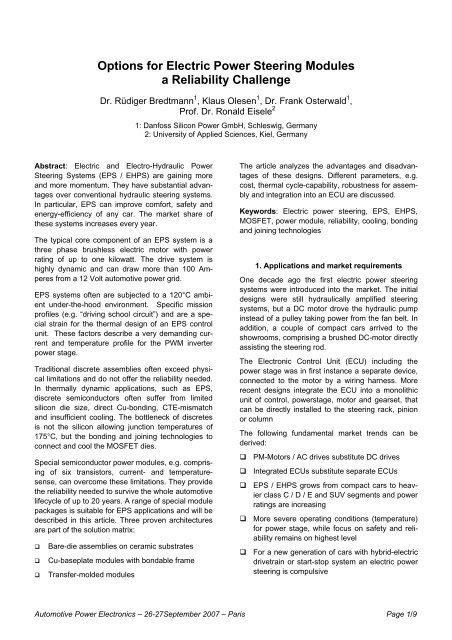
Options for Electric Power Steering Modules a Reliability ... - Danfoss
Options for Electric Power Steering Modules a Reliability ... - Danfoss
Options for Electric Power Steering Modules a Reliability ... - Danfoss

Create successful ePaper yourself
Turn your PDF publications into a flip-book with our unique Google optimized e-Paper software.
<strong>Options</strong> <strong>for</strong> <strong>Electric</strong> <strong>Power</strong> <strong>Steering</strong> <strong>Modules</strong><br />
a <strong>Reliability</strong> Challenge<br />
Dr. Rüdiger Bredtmann 1 , Klaus Olesen 1 , Dr. Frank Osterwald 1 ,<br />
Prof. Dr. Ronald Eisele 2<br />
Abstract: <strong>Electric</strong> and Electro-Hydraulic <strong>Power</strong><br />
<strong>Steering</strong> Systems (EPS / EHPS) are gaining more<br />
and more momentum. They have substantial advantages<br />
over conventional hydraulic steering systems.<br />
In particular, EPS can improve com<strong>for</strong>t, safety and<br />
energy-efficiency of any car. The market share of<br />
these systems increases every year.<br />
The typical core component of an EPS system is a<br />
three phase brushless electric motor with power<br />
rating of up to one kilowatt. The drive system is<br />
highly dynamic and can draw more than 100 Amperes<br />
from a 12 Volt automotive power grid.<br />
EPS systems often are subjected to a 120°C ambient<br />
under-the-hood environment. Specific mission<br />
profiles (e.g. “driving school circuit”) and are a special<br />
strain <strong>for</strong> the thermal design of an EPS control<br />
unit. These factors describe a very demanding current<br />
and temperature profile <strong>for</strong> the PWM inverter<br />
power stage.<br />
Traditional discrete assemblies often exceed physical<br />
limitations and do not offer the reliability needed.<br />
In thermally dynamic applications, such as EPS,<br />
discrete semiconductors often suffer from limited<br />
silicon die size, direct Cu-bonding, CTE-mismatch<br />
and insufficient cooling. The bottleneck of discretes<br />
is not the silicon allowing junction temperatures of<br />
175°C, but the bonding and joining technologies to<br />
connect and cool the MOSFET dies.<br />
Special semiconductor power modules, e.g. comprising<br />
of six transistors, current- and temperaturesense,<br />
can overcome these limitations. They provide<br />
the reliability needed to survive the whole automotive<br />
lifecycle of up to 20 years. A range of special module<br />
packages is suitable <strong>for</strong> EPS applications and will be<br />
described in this article. Three proven architectures<br />
are part of the solution matrix:<br />
� Bare-die assemblies on ceramic substrates<br />
� Cu-baseplate modules with bondable frame<br />
� Transfer-molded modules<br />
1: <strong>Danfoss</strong> Silicon <strong>Power</strong> GmbH, Schleswig, Germany<br />
2: University of Applied Sciences, Kiel, Germany<br />
The article analyzes the advantages and disadvantages<br />
of these designs. Different parameters, e.g.<br />
cost, thermal cycle-capability, robustness <strong>for</strong> assembly<br />
and integration into an ECU are discussed.<br />
Keywords: <strong>Electric</strong> power steering, EPS, EHPS,<br />
MOSFET, power module, reliability, cooling, bonding<br />
and joining technologies<br />
1. Applications and market requirements<br />
One decade ago the first electric power steering<br />
systems were introduced into the market. The initial<br />
designs were still hydraulically amplified steering<br />
systems, but a DC motor drove the hydraulic pump<br />
instead of a pulley taking power from the fan belt. In<br />
addition, a couple of compact cars arrived to the<br />
showrooms, comprising a brushed DC-motor directly<br />
assisting the steering rod.<br />
The Electronic Control Unit (ECU) including the<br />
power stage was in first instance a separate device,<br />
connected to the motor by a wiring harness. More<br />
recent designs integrate the ECU into a monolithic<br />
unit of control, powerstage, motor and gearset, that<br />
can be directly installed to the steering rack, pinion<br />
or column<br />
The following fundamental market trends can be<br />
derived:<br />
� PM-Motors / AC drives substitute DC drives<br />
� Integrated ECUs substitute separate ECUs<br />
� EPS / EHPS grows from compact cars to heavier<br />
class C / D / E and SUV segments and power<br />
ratings are increasing<br />
� More severe operating conditions (temperature)<br />
<strong>for</strong> power stage, while focus on safety and reliability<br />
remains on highest level<br />
� For a new generation of cars with hybrid-electric<br />
drivetrain or start-stop system an electric power<br />
steering is compulsive<br />
Automotive <strong>Power</strong> Electronics – 26-27September 2007 – Paris Page 1/9
� Additional com<strong>for</strong>t / safety features like superimposed<br />
steering and rear wheel steering will require<br />
high-power electric actuation<br />
A fundamental scope is on finding the right trade-off<br />
between cost, per<strong>for</strong>mance and the imperative reliability.<br />
Globally, about 10 major steering system suppliers<br />
of are working on electric power steering. They rely<br />
on a couple of experienced partners specializing in<br />
customized electronic components.<br />
2. <strong>Power</strong> Electronic Requirements<br />
The design of an electronic control (ECU) unit <strong>for</strong><br />
power steering systems starts with a careful description<br />
of the mission profile and environment of operation.<br />
The fundamental difference between a direct drive<br />
EPS and a pump-operated EHPS is, that true servo<br />
application EPS puts a higher current- and temperature-cycling<br />
profile on the power stage of its control<br />
unit.<br />
In contrast, an electro-hydraulic unit usually operates<br />
on continuously low revs to sustain a specific system<br />
pressure. In case of high demand <strong>for</strong> steering aid,<br />
the pump powers up to provide maximum output.<br />
Typically, the maximum load is described by an outstanding<br />
test scenario, e.g. a parking lot test with<br />
repetitive high steering demand under concurrent<br />
high ambient temperature load.<br />
1<br />
4<br />
6<br />
2<br />
5<br />
3<br />
1. Bondable frame<br />
2. DC connection<br />
3. Capacitor,<br />
EMC Filter<br />
4. AC-Motor<br />
connection<br />
5. Integrated<br />
power module<br />
6. Control board<br />
Figure 1: Example of an ECU (Electronic Control<br />
Unit) <strong>for</strong> <strong>Electric</strong> <strong>Power</strong> <strong>Steering</strong><br />
The designer of an ECU must blend these external<br />
requirements with space and cost constraints in the<br />
control unit. To survive the described harsh test and<br />
operating conditions, a proper thermal management<br />
of the device is highly relevant.<br />
In the past often one single type of circuit carrier,<br />
e.g. glass-epoxy (FR4) or thickfilm-ceramics were<br />
sufficient to arrange the whole componentry of an<br />
ECU. Since currents are increasing substantially,<br />
specialized substrates <strong>for</strong> signal and power stage<br />
are moving into modern ECUs.<br />
Dedicated power modules allow to increase power<br />
density and can dissipate up to 10 W / cm². Alongside,<br />
they can be designed to take the strong thermal<br />
cycling loads coming <strong>for</strong> the extensive servo<br />
operation.<br />
3. Solution Overview <strong>Power</strong> <strong>Modules</strong><br />
3.1 Bare DBC Substrates<br />
The most simplistic PWM-power-stage can be demonstrated<br />
by a populated DBC-substrate. These<br />
substrates typically comprise a MOSFET six-pack to<br />
drive a three phase motor. MOSFETs are typically<br />
soldered with a virtually void-free alloy, that gives<br />
sufficient headroom between maximum operating<br />
temperature and the solder melting temperature.<br />
Figure 2: Bare DBC-Substrate with MOSFET-<br />
Transistors <strong>for</strong> glue-on-assembly<br />
The proven Al2O3-Substrates with a thermal expansion<br />
coefficient of 7-8 ppm/k are matching well with a<br />
silicon die of about 3 ppm/k.<br />
Ceramic substrates provide excellent isolation up to<br />
several thousand volts and are good heat conductors.<br />
The thick and homogenous Cu-coating on the<br />
DBC’s front and backside provides a good temperature<br />
distribution, lateral spreading and very low ohmic<br />
losses.<br />
Compared to usual 100 µm thickfilm-copper-glaspaste<br />
hybrids the electrical conductivity of a DBC is<br />
about 6 times higher.<br />
Automotive <strong>Power</strong> Electronics – 26-27 September 2007 – Paris Page 2/9
Figure 3: Multiple large wire bonds provide current<br />
distribution and minimised losses<br />
In addition, MOSFET semiconductors can be generously<br />
covered with a maximum of large-wire bonds<br />
in order to minimize ohmic losses and unwanted<br />
heat dissipation by eliminating hotspots.<br />
Unlike the simplistic nature of this device, its assembly<br />
is slightly more complicated than other alternatives.<br />
The pre-soldered DBC-substrates have to be glued<br />
on a heath sink under very controlled conditions.<br />
Thermal conductivity of the glue layer and its physical<br />
coherence are vital to the overall thermal per<strong>for</strong>mance.<br />
After the glue is temperature-cured, the<br />
DBC can be connected to the external control- and<br />
power-contacts with large-wire bonding. Finally, the<br />
device has to be protected with a silicon-gel cover on<br />
open dies and bond-feet. These processes require<br />
an above-average precision and cleanliness compared<br />
to standard electronic assemblies.<br />
3.2 Cu-baseplate modules with bondable frame<br />
A more sophisticated and extended version of the<br />
bare DBC is a power module with added copper<br />
baseplate and a bondable frame <strong>for</strong> external electrical<br />
connection of the power-stage.<br />
Here, the DBC is thermally linked to a Cu-plate by a<br />
large-area solder layer. The copper now helps to<br />
buffer and to spread heat dissipated by the MOSFET<br />
dies.<br />
An external frame allows connecting the module to<br />
the external circuit by welding or soldering. The com-<br />
plete housing of semiconductors gives the module<br />
additional robustness.<br />
Thermal buffer properties of the Cu-baseplate allow<br />
<strong>for</strong> less rigid requirements with regard to an even<br />
heath sink surface or to the tolerance of the applied<br />
thermal interface material (TIM). Overall, the added<br />
module complexity allows <strong>for</strong> simplified assembly<br />
and cost savings in the periphery.<br />
Figure 4: EPS <strong>Power</strong> module with Cu-baseplate<br />
and bondable frame<br />
3.3 <strong>Power</strong>-Module with transfer-molded housing<br />
Discrete and integrated components with a mold<br />
resin encapsulation have a long tradition in electronics.<br />
With advanced duroplastic materials the industry can<br />
today produce power modules comprising a complete<br />
sixpack inverter stage with MOSFETs or IGBT.<br />
Key to these large-scale components is a mold compound<br />
with adapted thermal expansion coefficient<br />
CTE as well as low shrinkage.<br />
The finished mold package is very rigid and allows to<br />
easily assembling the modules with standard electronic<br />
manufacturing lines.<br />
Automotive <strong>Power</strong> Electronics – 26-27 September 2007 – Paris Page 3/9
Figure 5: Molded module in die-on-substrate<br />
technology in different production steps<br />
Two fundamental variants of power modules are<br />
available:<br />
- A Module comprising a molded DBC in<br />
analogy to 3.1. together with an integrated<br />
leadframe allowing <strong>for</strong> external contacts.<br />
Here, the DBC is both a perfect isolation <strong>for</strong><br />
voltage and a thermal interface to the heatsink<br />
- A Module comprising of a leadframe only.<br />
This layout separates different segments of<br />
the leadframe <strong>for</strong> different circuit potentials.<br />
Semiconductors are directly soldered upon<br />
the copper surfaces. This leadframe can<br />
only be assembled on a heatsink with an<br />
electrically isolating layer of glue or thermal<br />
interface material. It is basically limited to<br />
low-voltage Mosfet applications.<br />
4. <strong>Reliability</strong> Discussion<br />
Designing a power module <strong>for</strong> “under the hood” applications<br />
is a challenge <strong>for</strong> several reasons:<br />
First of all the physical environment <strong>for</strong> the power<br />
module is extremely harsh featuring high ambient<br />
temperatures (in excess of 100°C, up to 5-600°C<br />
near the exhaust), vibration, humidity, salt mist etc.<br />
Secondly because the designer works under a tremendous<br />
cost pressure (the way of life in automo-<br />
tives) meaning that it is a challenge to af<strong>for</strong>d a sufficient<br />
amount of power silicon that would enable a<br />
reasonable low thermal resistance. Thirdly because<br />
size maters: The designer is most often required to<br />
integrate the power module in an ECU within a very<br />
limited space available; this by the way often rules<br />
out other technical solutions like discretes on IMS.<br />
Thus the design process is based on a number of<br />
tradeoffs and compromises, e.g. longer life demands<br />
bigger silicon chips but that drives cost and size the<br />
wrong way.<br />
The degradation of power electronic devices under<br />
high current densities (consequently high power<br />
dissipation) can be traced to several different load<br />
categories:<br />
� Continuous operation with small variations in<br />
the current profile<br />
� Single short time events with max current<br />
demand (period: few seconds)<br />
� Groups of load variations over several seconds<br />
to minutes<br />
In automotive application all 3 types of load pattern<br />
can be observed. Most of the power electronic applications<br />
are defined by specific load profiles.<br />
� Hydraulic power steering: continuous operation<br />
plus groups of load variations<br />
� <strong>Electric</strong> power steering groups of load variations<br />
of short duration<br />
� Start/Stop systems: Single short time events<br />
within 1 second<br />
� Mild hybrids: Single short time events plus<br />
groups of load cycles<br />
� Strong hybrids: Mostly continuous operation<br />
plus groups of load cycles interrupted by<br />
single events<br />
Typical failure modes of power modules are to be<br />
found in the assembly of the semiconductors and<br />
materials of the thermal stack. It is possible to dedicate<br />
specific failure modes to specific load cycles:<br />
� Bond wire lift-off is caused by current switching<br />
between >0 s and ~3 s<br />
� Die-solder layer is cracked by current load<br />
cycles between ~5 s and ~20 s<br />
� Large area solder layer degradation of the<br />
substrate is observed <strong>for</strong> temperature changes<br />
between 600 s to 6,000 s<br />
Automotive <strong>Power</strong> Electronics – 26-27 September 2007 – Paris Page 4/9
The lifetime of a power module is predetermined by<br />
the number of temperature cycles (of a definite temperature<br />
swing) a specific thermal stack is capable to<br />
survive. All failure modes are heavily accelerated by<br />
the level of operating (ambient) temperature: The<br />
higher the ambient temperature, the higher average<br />
operating temperature and the more destructive the<br />
failure modes are addressed by the different load<br />
cycles.<br />
4.1 Device temperatures<br />
The importance of device temperature is demonstrated<br />
in the study by ST microelectronics.<br />
Failure in Time (FIT)<br />
4500<br />
4000<br />
3500<br />
3000<br />
2500<br />
2000<br />
1500<br />
1000<br />
500<br />
Lambda@90%C.L.<br />
0<br />
0<br />
-500<br />
50 100 150 200<br />
Junction Temperature Tj (°C)<br />
Source: ST-Microelectronics <strong>Reliability</strong> Report 2002<br />
Figure 6: FIT vs. junction temperature<br />
Here it is seen that the failures in time start to increase<br />
dramatically at junction temperatures above<br />
120-130°C. The trend in the semiconductor business<br />
towards higher and higher device temperatures,<br />
approaching and even surpassing 200°C should be<br />
taken with great precaution. The bonding and joining<br />
technologies need to follow troop and this generates<br />
new challenges.<br />
4.2 Wire bond failure<br />
One of the lifetime limiting factors is the wire bond<br />
connection; it turns out that fast temperature cycles<br />
(power cycling) create so called bond wire lift offs.<br />
This is caused by the mismatch in the coefficient of<br />
thermal expansion (CTE) between the silicon chip<br />
(CTE = 3 ppm/K) and the aluminum bond wire (CTE<br />
= 24 ppm/K). As the temperature changes this mismatch<br />
will create stresses and strains in the Si/Al<br />
interface which again lead to fatigue cracking. The<br />
larger the temperature swing the fewer cycles to<br />
failure. This phenomenon is well understood and<br />
most often modeled using a Coffin & Manson approach<br />
[3]. The chart below shows the relationship<br />
between the number of cycles to failure and the size<br />
of the temperature swings.<br />
Figure 7: The relationship between the number of<br />
cycles to failure <strong>for</strong> a wire bond and the ΔT.<br />
Also seen in the Coffin & Manson chart is the dependency<br />
of the mean temperature around which the<br />
temperature swings occur: the larger the Tm the<br />
shorter the life even <strong>for</strong> the same ΔT; the chart features<br />
three sets of test results per<strong>for</strong>med at different<br />
mean temperatures (60°C, 80°C and 100°C). This<br />
shows that good control of the mean device temperature<br />
is important in the second order: good cooling<br />
reduces the ΔT but also the level, Tm, where it<br />
occurs.<br />
4.3 Baseplates and large area solder joints<br />
There<strong>for</strong>e the semiconductors have to be cooled as<br />
effectively as possible, meaning that the thermal<br />
stack, which defines the materials and geometries<br />
from junction to ambient, must be optimized. As an<br />
example designing the power module with a copper<br />
baseplate offers a better thermal per<strong>for</strong>mance as<br />
shown in the figure below:<br />
Automotive <strong>Power</strong> Electronics – 26-27 September 2007 – Paris Page 5/9
Figure 8: Effect of having a copper baseplate.<br />
The baseplate helps spreading the heat over a large<br />
area be<strong>for</strong>e the heat passes through the inevitable<br />
thermal interface material (TIM) thus improving<br />
things considerably: the thermal resistance and thus<br />
the junction temperature will become lower and life<br />
will be longer because the wire bonds will experience<br />
smaller ΔT’s at lower Tm’s. <strong>Power</strong> modules<br />
having a baseplate are less sensitive towards the<br />
quality of the TIM, like thermal conductivity, thickness<br />
variations and voids, compared to “DCB-only”<br />
modules. Additionally the baseplate offers a quality<br />
of ruggedness to the power module: the delicate<br />
DCB substrate will much less prone to breakage<br />
when riding a baseplate.<br />
Introducing the baseplate in the power module does<br />
not solve all problems though, it even creates new<br />
problems. The most important is that the large area<br />
solder joint between the DCB substrate and the<br />
baseplate too is damaged by temperature cycles.<br />
But whereas the wire bonds suffer from a large<br />
number of fast power cycles, it is the slow temperature<br />
cycles, arising from daily climatic changes combined<br />
with cold starts of the car, that threaten the<br />
integrity of the large area solder joint. The failure<br />
mode is well understood and it too can be modeled<br />
using Coffin&Manson approaches [4]. An example is<br />
shown in the chart below that shows the relationship<br />
between number of cycles to failure and the size of<br />
the solder joint.<br />
1<br />
0 10 20 30 40 50<br />
Automotive <strong>Power</strong> Electronics – 26-27 September 2007 – Paris Page 6/9<br />
No. of cycles to failure N f<br />
100000<br />
10000<br />
1000<br />
100<br />
10<br />
lower bound<br />
DCB on Cu base plate<br />
h = 0.2 mm, ΔT = 130 K<br />
upper bound<br />
Radius from centre of DCB [mm]<br />
Al 2 O 3<br />
AlN<br />
Figure 9: The relationship between the size of the<br />
DBC substrate and the number of cycles to failure<br />
<strong>for</strong> a large are solder joint.<br />
It turns out that Nf is inversely proportional to the<br />
size (radius) of the solder joint squared and proportional<br />
to the thickness squared. This means that Nf is<br />
quadrupled by doubling the solder thickness but<br />
reduced to ¼th by doubling the size (radius) of the<br />
solder joint.<br />
Designing <strong>for</strong> optimum solder joint reliability involves<br />
optimizing the size of the solder joint i.e. length,<br />
width and thickness.<br />
4.4 The mission profile of power steering applications<br />
- Requirements<br />
Understanding all the relevant failure mechanisms of<br />
the power module assembly and knowing the load<br />
conditions that the module will see during its life of<br />
operation, the mission profile, are the keystones <strong>for</strong><br />
the most optimum design of the power module.<br />
The design process is an iterative one: The temperature<br />
cycles that define the mission profile are analyzed<br />
individually regarding their damaging effect on<br />
the wire bonds, solder joints etc.; the sum of these<br />
individual damaging effects then <strong>for</strong>m the overall<br />
damaging effect arising from the mission profile.<br />
If it turns out that the power module will fail too soon,<br />
e.g. by wire bond lift off, the thermal design must be<br />
improved as to lower the size of the temperature<br />
swings and/or by lowering the mean temperature.<br />
This most often demands larger silicon chips and/or<br />
an improved cooling.<br />
If, on the other hand, the power module will survive<br />
the loads defined by the mission profile by too large<br />
a margin, the module is thermally oversized and thus
too costly. The thermal stack must be trimmed down<br />
e.g. by reducing silicon area.<br />
The basis <strong>for</strong> the thermal design approach described<br />
above is the specification; a clear definition of the<br />
mission profile is crucial in order to do an optimum<br />
design that will withstand the required load cycles<br />
without being “overkill” and a too costly design.<br />
One of most important in<strong>for</strong>mation <strong>for</strong> the module<br />
designer is the number of operating hours and the<br />
temperature level. Typically the demand is 6,000h of<br />
operation under varying boundary conditions of ambient<br />
temperature and load induced temperature<br />
swings.<br />
45%<br />
40%<br />
35%<br />
30%<br />
25%<br />
20%<br />
15%<br />
10%<br />
5%<br />
0%<br />
Operating Temperaure<br />
Frequency Distribution over Lifetime<br />
-25 40 80 90 100 105 110 115 120<br />
Figure 10: Operating temperature as frequency<br />
distribution of lifetime<br />
A typical assumption <strong>for</strong> the ambient temperature is<br />
34% of the operating period is below 85°C, 63% of<br />
the time the ambient temperature is between 80°C<br />
and 100°C and only 3% above 100°C<br />
The second step is to define a real or at least realistic<br />
load cycle followed by trans<strong>for</strong>mations from current<br />
profiles into power losses profiles and from<br />
there to temperature swings at a given ambient temperature.<br />
I [A]<br />
400<br />
300<br />
200<br />
100<br />
-200<br />
-300<br />
-400<br />
[°C]<br />
Current vs. time<br />
0<br />
0 50 100 150 200 250 300 350 400<br />
-100<br />
Time [sec]<br />
Figure 11: A logged current profile of an electrical<br />
vehicle in movement. Note the negative current<br />
during recuperation<br />
Thermal response<br />
0<br />
0 50 100 150 200<br />
Time [sec]<br />
250 300 350 400<br />
Automotive <strong>Power</strong> Electronics – 26-27 September 2007 – Paris Page 7/9<br />
Temperature rise [K]<br />
20<br />
15<br />
10<br />
5<br />
Fig. 12: Thermal response of the junction temperature<br />
of a MOSFET of an electric vehicle deducted<br />
from the current profile and the Rth of the<br />
power module in the system<br />
The temperature change by power losses of the<br />
device (see Fig. 12) and ambient temperatures of<br />
80°c to 110°C leads junction temperatures up to<br />
160°C (see Fig. 10) is the critical factor <strong>for</strong> the degradation.<br />
The following graph indicates the estimation of the<br />
frequency distribution of the junction temperature in<br />
a power steering module during 6000 hours of operation.<br />
Junction temperature does not exceed 160°C under<br />
worst conditions (lock stop, short circuit, etc. at<br />
maximum operating temperature under the hood).<br />
This is called a ‘safe design’.<br />
40%<br />
35%<br />
30%<br />
25%<br />
20%<br />
15%<br />
10%<br />
5%<br />
0%<br />
Junction Temperaure<br />
Frequency Distribution over Lifetime<br />
210<br />
Figure 13: Junction temperature of a MOSFET<br />
power module in a power steering application. Tj<br />
is obtained with operating temperatures based<br />
on Figure 10
5. Cost drivers<br />
The three different module types have not only different<br />
physical characteristics. They differ in cost as<br />
well. To find a proper solution, a total cost of ownership-calculation<br />
can be recommended.<br />
The bare DBC is obviously least in cost. But its assembly<br />
process requires higher investment and / or<br />
labor content than the more complex housed variants.<br />
6. Conclusion<br />
<strong>Danfoss</strong> Silicon <strong>Power</strong> is convinced that a reliable<br />
and economic solution will be created holistically,<br />
integrating the mechanical, electrical and thermal<br />
design of the power module and its application.<br />
EPS <strong>Power</strong>-<strong>Modules</strong> <strong>Power</strong> <strong>Modules</strong> compared<br />
Bare DBC<br />
Subject<br />
1 Thermal Cycles<br />
high<br />
medium<br />
medium - high<br />
2 <strong>Power</strong> density<br />
medium<br />
high<br />
high<br />
3 Thermal robustness sensitive<br />
high<br />
high<br />
4 Assembly process sophisticated<br />
standard<br />
standard<br />
5 Cost<br />
low medium low - medium<br />
Recommended<br />
<strong>for</strong> Application<br />
Source: <strong>Danfoss</strong> Research<br />
EPS / EHPS<br />
various drives<br />
Figure 14: Evaluation overview<br />
Cu baseplate<br />
EHPS, power<br />
management<br />
Molded Module<br />
EPS / EHPS<br />
various drives<br />
In this article, a range of three options was discussed.<br />
Each of these has specific advantages. The<br />
bare DBC is a very simplistic approach that has<br />
been proven in millions of vehicles. Its limitations<br />
stem from the thermal stack and a glue-layer that<br />
can constrain the cooling of semiconductors.<br />
The copper baseplate module can be considered the<br />
“silver bullet” with regard to thermal robustness. No<br />
other solution in particular can equal the thermal<br />
robustness and tolerance to variations of the thermal<br />
interface together with excellent voltage isolation.<br />
A fully molded power module with copper interface is<br />
mechanically very robust. Its voltage isolation is<br />
restricted to the usual 12-Volt range. In contrast, the<br />
thermal buffer capability of a copper leadframe can<br />
be superior to the glued DBC variant.<br />
Now it is the designer’s choice to make up their individual<br />
evaluation matrix!<br />
7. References<br />
[] ST-Microelectronics, “<strong>Reliability</strong> Report ST-<br />
Microelectronics; D²PAK RELIABILITY DATA,<br />
HTRB, Low Threshold <strong>Power</strong> Mos Transistor”<br />
[2] Olesen et. Al. “Practical Thermal Management”,<br />
Chapter 8, page 75-99, SPM, Society of <strong>Reliability</strong><br />
and Environmental Testing, Denmark 2006.<br />
[3] Schulz, Kock “Abschlußbericht für BMBF Verbundprojekt<br />
Ultra-Le-MOS”, Schleswig, Oktober 2006<br />
[4] Held, Jacob, Nicoletti, Scacco, Poech, Fast power<br />
cycling test <strong>for</strong> IGBT modules in traction applications,<br />
Proc. Conf. <strong>Power</strong> Electronics and Drive Systems,<br />
1997, 425-430<br />
[5] Herr, Frey, Schlegel, Stuck, Zehringer, Substrateto-base<br />
solder joint reliability in high power IGBT<br />
modules, Microelectronics <strong>Reliability</strong> 37, 1997, No.<br />
10/11, 1719-1722<br />
[6] Poech, Eisele, A modelling approach to assess the<br />
creep behaviour of large-area solder joints, Microelectronics<br />
<strong>Reliability</strong> 40, 2000, 1653-1658<br />
[7] Schrüllkamp, <strong>Steering</strong> Systems – A Challenge of<br />
Market and Technologies, Conference Presentation,<br />
<strong>Steering</strong> Systems 2007, Bonn<br />
Automotive <strong>Power</strong> Electronics – 26-27 September 2007 – Paris Page 8/9
8. Authors<br />
Dr. Rüdiger Bredtmann is Director<br />
Customer Relations <strong>for</strong> the<br />
automotive industry at <strong>Danfoss</strong><br />
Silicon <strong>Power</strong> GmbH. His scientific<br />
focus is power electronics<br />
<strong>for</strong> automotive traction drives /<br />
hybrid electric vehicles and other<br />
high current ECU applications in<br />
cars. He holds a PhD in <strong>Electric</strong>al<br />
Engineering from the Berlin<br />
University of Technology and a<br />
Master of Business Administration of WHU / Kellogg<br />
School of Management, Koblenz / Evanston (USA).<br />
Klaus Olesen works in the R&D<br />
department of <strong>Danfoss</strong> Silicon<br />
<strong>Power</strong> GmbH where he works with<br />
new cooling concepts <strong>for</strong> power<br />
electronics and is responsible <strong>for</strong><br />
reliability assessments and thermal/mechanical<br />
simulations. He<br />
holds a M. Sc. in physics and<br />
mathematics from the University of<br />
Aarhus in Denmark.<br />
Dr. Frank Osterwald is Director <strong>for</strong><br />
Research and Development at<br />
<strong>Danfoss</strong> Silicon <strong>Power</strong> GmbH. His<br />
research topics are the packaging<br />
of power semiconductors and<br />
bonding and joining technologies.<br />
He holds a PhD in <strong>Electric</strong>al<br />
Engineering from the Berlin<br />
University of Technology.<br />
Dr. Ronald Eisele is Professor <strong>for</strong><br />
Sensors & Technology in the Institute<br />
of Mechatronics at the University<br />
of Applied Sciences in Kiel,<br />
Germany. He is working on bonding<br />
and joining techniques especially<br />
related to component packaging<br />
and liquid cooling of devices<br />
and their characterization.<br />
Contact:<br />
<strong>Danfoss</strong> Silicon <strong>Power</strong> GmbH, Heinrich-Hertz-Strasse 2,<br />
D-24876 Schleswig, Tel.: +49 (0) 46 21 – 95 12 – 394,<br />
E-mail: rbm@danfoss.com<br />
Automotive <strong>Power</strong> Electronics – 26-27 September 2007 – Paris Page 9/9