of MEMS - Institute of Microelectronics - A*Star
of MEMS - Institute of Microelectronics - A*Star
of MEMS - Institute of Microelectronics - A*Star

You also want an ePaper? Increase the reach of your titles
YUMPU automatically turns print PDFs into web optimized ePapers that Google loves.
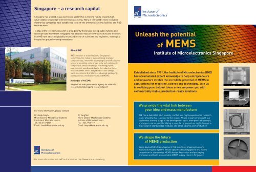
Singapore – a research capital<br />
Singapore has a world-class electronics sector that is moving rapidly towards high<br />
value-added, knowledge-intensive manufacturing. Many <strong>of</strong> the world’s most innovative<br />
electronics companies have established state-<strong>of</strong>-the art manufacturing facilities and R&D<br />
facilities here.<br />
To stay at the forefront, research is a top priority that enjoys strong public funding and<br />
record private investment. Singapore has excellent research infrastructure and institutes<br />
like IME have attracted globally respected research scientists and engineers, making it a<br />
hotspot for groundbreaking innovations.<br />
For more information, please contact:<br />
Dr Janak Singh<br />
Micro-Electro-Mechanical-Systems<br />
<strong>Institute</strong> <strong>of</strong> <strong>Microelectronics</strong><br />
Tel: +65 6770 5909<br />
Email: Janak@ime.a-star.edu.sg<br />
About IME<br />
IME’s mission is to add value to Singapore’s<br />
semiconductor industry by developing strategic<br />
competencies, innovative technologies and intellectual<br />
property; enabling enterprises to be technologically<br />
competitive; and cultivating a technology talent<br />
pool to inject new knowledge to the industry. Its key<br />
research areas are in integrated circuits design,<br />
nano-electronics & photonics, advanced packaging,<br />
bioelectronics, medical devices and <strong>MEMS</strong>.<br />
A member <strong>of</strong> A*STAR<br />
Singapore’s lead government agency for scientific<br />
research and developing research talent<br />
Dr Tang Min<br />
Micro-Electro-Mechanical-Systems<br />
<strong>Institute</strong> <strong>of</strong> <strong>Microelectronics</strong><br />
Tel: +65 6770 5769<br />
Email: tangm@ime.a-star.edu.sg<br />
For more information, visit IME on the Internet: http://www.ime.a-star.edu.sg.<br />
Unleash the potential<br />
<strong>of</strong> <strong>MEMS</strong><br />
<strong>Institute</strong> <strong>of</strong> <strong>Microelectronics</strong> Singapore<br />
Established since 1991, the <strong>Institute</strong> <strong>of</strong> <strong>Microelectronics</strong> (IME)<br />
has accumulated expert knowledge to help entrepreneurs<br />
and innovators stretch the incredible potential <strong>of</strong> <strong>MEMS</strong> in<br />
applications for medicine, science and technology. Join us<br />
in realizing your boldest ideas as we empower you with<br />
commercially viable, production-ready solutions.<br />
We provide the vital link between<br />
your idea and mass manufacture<br />
IME has a dedicated R&D foundry, staffed by a highly experienced research<br />
team–a facility that is unique to the region. We are in partnership with our<br />
customers at every stage <strong>of</strong> the development cycle, from pro<strong>of</strong>-<strong>of</strong>-concept,<br />
prototype creation and identifying a manufacturing partner right through to<br />
the design <strong>of</strong> standardized modules and small volume pilot production.<br />
We shape the future<br />
<strong>of</strong> <strong>MEMS</strong> production<br />
Going beyond <strong>MEMS</strong> development, IME is actively shaping its entire<br />
manufacturing eco-system. We are spearheading Singapore’s first <strong>MEMS</strong><br />
consortium to standardize <strong>MEMS</strong> design, fabrication and packaging<br />
processes and build a sustainable <strong>MEMS</strong> supply chain in Singapore.
Access a unique facility<br />
like no other<br />
IME <strong>of</strong>fers fabless and fab-lite customers access<br />
to the region’s first and only R&D foundry where<br />
experienced research teams are on hand to<br />
support every need with a full suite <strong>of</strong> research and<br />
development services. Take advantage <strong>of</strong> IME’s fully<br />
integrated <strong>MEMS</strong> design, fabrication packaging and<br />
characterization capabilities and our proven expertise<br />
in <strong>MEMS</strong> and CMOS integration to achieve costeffective<br />
production.<br />
R&D FOUnDRy BUSInESS MODEl<br />
IME: R&D Partner<br />
• Facility, Expertise,<br />
Solutions, IPs<br />
• Prototyping and<br />
Qualification<br />
Fabless Product Company<br />
Enter the future <strong>of</strong> <strong>MEMS</strong> manufacturing<br />
Manufacturing Partner<br />
• Wafer fabs; Equipment<br />
Seller<br />
• Packaging/Assembly;<br />
Substrates<br />
Backed by A*STAR and the Economic Development<br />
Board, IME has mobilized industry players from every<br />
stage <strong>of</strong> the <strong>MEMS</strong> supply chain to form the Singapore<br />
<strong>MEMS</strong> Consortium. This game-changing collaboration<br />
promotes the manufacturing <strong>of</strong> <strong>MEMS</strong> devices for<br />
multiple applications using standardized technology<br />
platforms.<br />
Ultimately, our success can help you lower costs and<br />
other barriers to entry, increase productivity and<br />
speed up the growth <strong>of</strong> a sustainable <strong>MEMS</strong> industry in<br />
Singapore capable <strong>of</strong> meeting urgent global demand.<br />
8” wafer fab facilities for CMOS and <strong>MEMS</strong> prototyping<br />
A 2100m2 , Class 1/100 clean room with state-<strong>of</strong>the-art<br />
8” wafer fabrication equipment and separate<br />
clean rooms for <strong>MEMS</strong> and CMOS to avoid crosscontamination.<br />
Packaging, assembly and microsystem technology<br />
Advanced equipment for photonics, bio, nano and SiP<br />
packaging and assembly, as well as thermal, electrical,<br />
mechanical and optical modeling and simulation<br />
expertise under one ro<strong>of</strong>.<br />
Materials characterization and failure analysis<br />
expertise<br />
A full set <strong>of</strong> analytical and test support services<br />
(M-STEM, TEM, SEM, Auger, SIMS, TXRF, FIB, AFM, FTIR)<br />
State-<strong>of</strong>-the-art laboratories<br />
• Circuit Design Lab with industry standard CAD tools<br />
for RF, Analog, Mixed-Signal and Digital designs<br />
• High-frequency device characterization Lab featuring<br />
110GHz characterization equipment with 12-inch<br />
wafer prober<br />
• Optoelectronics and photonics Lab with full set<br />
<strong>of</strong> characterization set-ups for 10 Gb/s and above<br />
testing<br />
• Organic electronics Lab with full sets <strong>of</strong> processing<br />
tools and capabilities for OPV<br />
• Bio Lab featuring micr<strong>of</strong>luidics-based platforma for<br />
nucleic acid, protein and cells analyses<br />
Device Design and<br />
Modeling<br />
Available<br />
Available<br />
• Resonator<br />
(Piezoelectric/<br />
Electrostatic type)<br />
• Low power Signal<br />
conditioning &<br />
processing circuits<br />
• Actuator<br />
(ES/ Thermal/<br />
Piezo)<br />
• RF <strong>MEMS</strong> switch<br />
for capacitive<br />
accelerometer and<br />
pressure sensor<br />
(Capacitive/<br />
metal-contact type)<br />
• Magnetic and<br />
• Wireless link<br />
transceiver circuits<br />
NEMS switch • <strong>MEMS</strong> display<br />
• Accelerometer driver signal<br />
(2D/ 3D)<br />
• Pressure sensor<br />
conditioning circuits<br />
• NEMS pressure Upcoming<br />
sensor<br />
• Signal conditioning<br />
• Micro-mirror & processing<br />
• IR sensor<br />
circuits for<br />
• Piezoelectric filter Biomedical<br />
& impedance<br />
tuner<br />
applications<br />
• Energy harvester<br />
(Thermoelectric /<br />
Capacitive)<br />
• RF <strong>MEMS</strong>-based<br />
transceiver<br />
Upcoming<br />
• Ultrasonic<br />
transducer<br />
Partner the Best<br />
With two decades <strong>of</strong> expertise in <strong>MEMS</strong> research and firsthand experience shaping the industry, IME is<br />
the research partner <strong>of</strong> choice.<br />
Benefits<br />
<strong>MEMS</strong> ASIC<br />
Design Capability<br />
IME <strong>MEMS</strong> Core Capabilities<br />
<strong>MEMS</strong> Process<br />
Technology<br />
Available<br />
• Bulk & surface<br />
micromachining<br />
• Wafer bonding<br />
(direct & adhesive)<br />
• VHF/XeF 2 release &<br />
anti-stiction coating<br />
• Bio-compatible<br />
polymers<br />
• CMOS & <strong>MEMS</strong><br />
integration<br />
• Stress compensation<br />
thin film processes<br />
• Sacrificial polymer<br />
via fill process<br />
and suspended<br />
microstructures<br />
• Void free Cu and<br />
Polysilicon TSV<br />
technology<br />
Upcoming<br />
• Low-temp C2W<br />
packaging<br />
• Thin film<br />
encapsulation<br />
• <strong>MEMS</strong>-ASIC 3D stack<br />
with TSV<br />
<strong>MEMS</strong> Packaging<br />
Technology<br />
Available<br />
• Micro fluidic<br />
packaging process<br />
• Wafer thinning with<br />
capped wafer<br />
• WLP by Frit-glass &<br />
solder bonding<br />
• Hermetic & vacuum<br />
WLP (Frit-glass and<br />
solder-based)<br />
• Released <strong>MEMS</strong><br />
wafer dicing<br />
• TSV for surface<br />
mountable WLP<br />
• Embedded packaging<br />
• Packages with small<br />
form factor<br />
(e.g. < 1mm x 1mm)<br />
Upcoming<br />
• Low-temp C2W<br />
vacuum packaging<br />
• Thin film<br />
encapsulation<br />
• <strong>MEMS</strong> & ASIC 3D<br />
stacking with TSV<br />
• Strong intellectual property protection with no conflict <strong>of</strong> interest from partners<br />
• Production-ready research strategy and third-party manufacturing partner involvement<br />
• Extensive industry and academic network<br />
• Strategic location in Singapore with in-depth insights and ready access to regional markets<br />
<strong>MEMS</strong> Device<br />
Characterization<br />
Available<br />
• Resonant frequency<br />
(using Impedance<br />
Analyzer & MMA)<br />
• Quality factor vs<br />
pressure<br />
(in vacuum chamber)<br />
• Motion analysis<br />
(using MMA)<br />
• Surface pr<strong>of</strong>ile<br />
(using WYKO)<br />
• Accelerometer<br />
(CV & ASIC)<br />
• Energy harvester<br />
• Pressure sensor<br />
(temp & pressure<br />
chamber)<br />
• Optical <strong>MEMS</strong><br />
(Optical bench with<br />
laser source)<br />
• Mode shape, in-plane<br />
and out-<strong>of</strong>-plane<br />
motion (using MSA<br />
motion analyzer)<br />
• RF S-parameter<br />
measurement