Ultrapure, high mobility organic photoconductors
Ultrapure, high mobility organic photoconductors
Ultrapure, high mobility organic photoconductors
You also want an ePaper? Increase the reach of your titles
YUMPU automatically turns print PDFs into web optimized ePapers that Google loves.
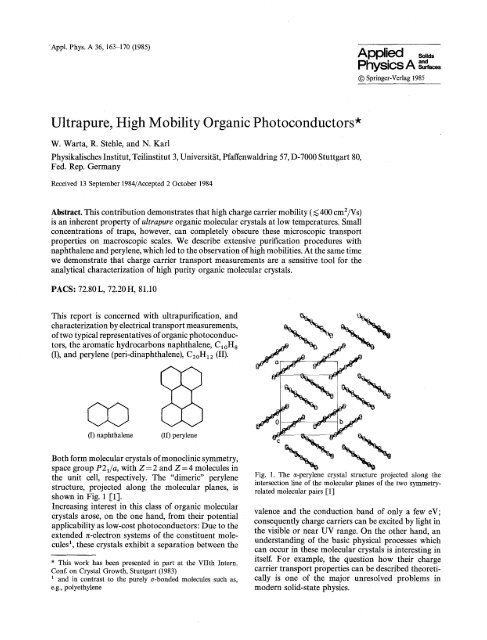
'Appl. Phys. A 36, 163-170 (1985)<br />
<strong>Ultrapure</strong>, High Mobility Organic Photoconductors*<br />
W. Warta, R. Stehle, and N. Karl<br />
Physikalisches Institut, Teilinstitut 3, Universit/it, Pfaffenwaldring 57, D-7000 Stuttgart 80,<br />
Fed. Rep. Germany<br />
Received 13 September 1984/Accepted 2 October 1984<br />
Abstract. This contribution demonstrates that <strong>high</strong> charge carrier <strong>mobility</strong> (< 400 cm2/Vs)<br />
is an inherent property of ultrapure <strong>organic</strong> molecular crystals at low temperatures. Small<br />
concentrations of traps, however, can completely obscure these microscopic transport<br />
properties on macroscopic scales. We describe extensive purification procedures with<br />
naphthalene and perylene, which led to the observation of <strong>high</strong> mobilities. At the same time<br />
we demonstrate that charge carrier transport measurements are a sensitive tool for the<br />
analytical characterization of <strong>high</strong> purity <strong>organic</strong> molecular crystals.<br />
PACS: 72.80L, 72.20H, 81.10<br />
This report is concerned with ultrapurification, and<br />
characterization by electrical transport measurements,<br />
of two typical representatives of <strong>organic</strong> photoconduc-<br />
tors, the aromatic hydrocarbons naphthalene, C~0H8<br />
(I), and perylene (peri-dinaphthalene), C2oH12 (II).<br />
(I) naphthalene (i1) perylene<br />
Both form molecular crystals of monoclinic symmetry,<br />
space group P21/a, with Z = 2 and Z = 4 molecules in<br />
the unit cell, respectively. The "dimeric" perylene<br />
structure, projected along the molecular planes, is<br />
shown in Fig. 1 F1].<br />
Increasing interest in this class of <strong>organic</strong> molecular<br />
crystals arose, on the one hand, from their potential<br />
applicability as low-cost <strong>photoconductors</strong>: Due to the<br />
extended re-electron systems of the constituent mole-<br />
cules 1, these crystals exhibit a separation between the<br />
* This work has been presented in part at the VIIth Intern.<br />
Conf. on Crystal Growth, Stuttgart (1983)<br />
1 and in contrast to the purely or-bonded molecules such as,<br />
e.g., polyethylene<br />
ill/<br />
Applied .o,,..<br />
Physics A Surfar<br />
9 Springer-Verlag 1985<br />
Fig. 1. The e-perylene crystal structure projected along the<br />
intersection line of the molecular planes of the two symmetry-<br />
related molecular pairs [1]<br />
valence and the conduction band of only a few eV;<br />
consequently charge carriers can be excited by light in<br />
the visible or near UV range. On the other hand, an<br />
understanding of the basic physical processes which<br />
can occur in these molecular crystals is interesting in<br />
itself. For example, the question how their charge<br />
carrier transport properties can be described theoreti-<br />
cally is one of the major unresolved problems in<br />
modern solid-state physics.
164 W. Warta et al.<br />
The investigations presented here are part of a larger<br />
program designed to obtain reliable experimental data<br />
over wide temperature ranges on charge-cartier trans-<br />
port in <strong>organic</strong> <strong>photoconductors</strong>. Naphthalene and<br />
perylene were selected, among others, to serve as model<br />
substances. Naphthalene is one of the most simple<br />
aromatic molecules; very extensive investigations are<br />
available of both its molecular and its crystal pro-<br />
perties. Its melting point, however, (m.p. = 80.5 ~ is<br />
too low for any potential practical application. In<br />
contrast, perylene, which melts at 278 ~ is an example<br />
of a fairly stable, larger aromatic molecule. Both<br />
materials can be zone-refined and obtained as fairly<br />
perfect single crystals by the Bridgman method.<br />
We have chosen not to measure the electrical conduc-<br />
tivity as such, since it is in the most general case<br />
composed of at least four independent material pro-<br />
perties: the electron and hole concentrations, n- and<br />
n +, and the electron and hole mobilities, #- and #+,<br />
respectively<br />
= e(n-#- + n+#+). (1)<br />
Instead, we decided to focus on the basic transport<br />
quantities, #- and/~+. These mobilities can, in prin-<br />
ciple, be measured separately by the time-of-flight<br />
technique, cf. [2], where the transit of electrons<br />
or holes over macroscopic sample dimensions (of<br />
typically 0.2-1 ram) is observed.<br />
However, most chemical impurities can very efficiently<br />
capture charge carriers during passage through the<br />
crystal, because the wide band gaps which are typical<br />
for this material class provide a wide energy range in<br />
which impurity states can act as traps. It is therefore<br />
crucial to study charge carrier transport properties at<br />
extremely low impurity concentrations. In addition,<br />
the concentration of physical (lattice) defects has to be<br />
kept low by careful annealing and handling of the<br />
crystals, since at the present level of chemical purity,<br />
physical defects can no longer be considered to give rise<br />
to only minor contributions for the total trapping<br />
behaviour.<br />
Traps which are energetically deep with respect to kT<br />
can completely prohibit the observation of carrier<br />
transits. Shallow traps can repeatedly hold charge<br />
carriers for short time intervals, until they are<br />
thermally released to the conduction states again. A<br />
strongly reduced, thermally activated "effective" mo-<br />
bility is therefore commonly observed in such cases,<br />
cf. [3]. The intrinsic transport properties, the "micro-<br />
scopic" mobilities (or "lattice mobilities") are ob-<br />
scured in such situations. Early <strong>mobility</strong> results have<br />
often suffered from these different trapping influences.<br />
(This is at least and definitely known to be so in<br />
cases where more efficient purification later led to<br />
<strong>high</strong>er, non-thermally activated <strong>mobility</strong> values.)<br />
Historically, the measured microscopic mobilities were<br />
often on the order of 1 cm2/Vs, cf. [4, 5] which is very<br />
small in comparison with the mobilities in standard<br />
in<strong>organic</strong> semiconductors, such as silicon or ger-<br />
manium. An increase of the mobilities # with decreas-<br />
ing temperature T, # oc T", (n < 0), was found with some<br />
of the purer samples: This increase was usually re-<br />
stricted to narrow temperature intervals near room<br />
temperature (and therefore not very big). The reason is<br />
that even very shallow trapping influences, not seri-<br />
ously disturbing room-temperature transport, can<br />
limit the observability of transits at lower tempera-<br />
tures, since the time constants for thermal detrapping<br />
increase exponentially on cooling. The reproducibility<br />
of mobifity results was sometimes rather poor between<br />
different laboratories, which may also have been due to<br />
(unknown) impurities which were present in variable<br />
amounts in the different samples.<br />
There were only three cases reported in the literature<br />
where crystal quality permitted reaching lower tem-<br />
peratures: The electron-<strong>mobility</strong> tensor component<br />
#~;~, in anthracene was measured down to liq. N2<br />
temperature [4, 6]; (surprisingly it exhibited the ab-<br />
normality of remaining nearly temperature-<br />
independent between 373 and 83 K, amounting to<br />
0.4cmZ/Vs). In naphthalene the observation of a<br />
transition from a nearly temperature-independent<br />
electron-<strong>mobility</strong> tensor component #~;c. = 0.4 cm2/Vs<br />
to one rising exponentially below 120 K was accom-<br />
plished in a measurement down to 31 K, where #~c.<br />
=2cmZ/Vs was reached [7]. Durene was the only<br />
example for which fairly <strong>high</strong> low-temperature mo-<br />
bilities have been reported (#+ = 55 cmZ/Vs at 120 K)<br />
[83.<br />
The aim of the work presented here was to improve<br />
purification procedures and to grow <strong>high</strong>-quality<br />
single crystals of naphthalene and perylene in order to<br />
find out if and to which maximum value intrinsic<br />
charge carrier mobilities continue to increase with<br />
decreasing temperature, and, if <strong>high</strong> charge carrier<br />
mobilities might eventually constitute a common low-<br />
temperature property of aromatic crystals.<br />
On our way to gradually increased purities we found,<br />
among other things, that temperature-dependent<br />
charge carrier <strong>mobility</strong> measurements represent a very<br />
sensitive analytical tool for the assessment of purity<br />
of <strong>organic</strong> aromatic crystals and we wish to focus on<br />
this aspect in this publication.<br />
Purification Procedures<br />
We started with the purest commercially available<br />
material (naphthalene "for scintillation", Merck, pery-<br />
lene "purum", Fluka). Naphthalene was prepurified by<br />
liquid chromatography. After vacuum sublimation,
<strong>Ultrapure</strong>, High Mobility Organic Photoconductors 165<br />
z<br />
the major part of the impurities was removed by an<br />
initial zone refining step, consisting of 100 zones passed<br />
across the naphthalene and perylene tubes at a speed of<br />
10 mm/h. Two impurities in naphthalene,<br />
//-methylnaphthalene and thionaphthene, are hard to<br />
deplete below 1 ppm by zone refining, because at lower<br />
concentrations they exhibit distribution coefficients<br />
close to one. In this ease (as in others, such as pyrene)<br />
treatment with molten potassium [9] (of. [10]) was<br />
applied in order to chemically modify the distribution<br />
coefficients of these persistent impurities by transform-<br />
ing them to reaction products with a more favorable<br />
distribution coefficient, or to non-volatile potassium<br />
salts which remain in the residue in a subsequent<br />
sublimation step. The principle of potassium fusion is<br />
sketched in Fig. 2 [,10]. The material is sublimed<br />
through a sequence of adsorbents (teflon wool, t,<br />
charcoal, c, and 4 fi, molecular sieves, m) into a reaction<br />
flask, 2, which had been coated with a potassium<br />
mirror. The molten components are allowed to react<br />
for about 12 hours. This step is repeated twice. Sub-<br />
sequently, the purified material is collected in zone<br />
refining tubes, z, for the main zone refinement. Pre-<br />
zonerefined perylene was used without potassium<br />
treatment. In three following zone refining steps a total<br />
number of about 500 molten zones were passed in a<br />
similar way across the naphthalene and the perylene<br />
ingots.<br />
The first step consisted in a normal vertical zone<br />
refinement, using a multistage intermittent technique.<br />
Then reverse horizontal zone refinement followed. For<br />
this purpose, the material was transferred to a nar-<br />
rower zone refining tube after removal of the impure<br />
ends (~ 15% at each side). Finally, another normal<br />
vertical zone refining step was applied, using a zone-<br />
refining tube equipped with a break seal. This break<br />
seal can be opened under vacuum conditions, allowing<br />
transfer (under complete exclusion of air) of the purest<br />
I<br />
I<br />
3x<br />
I m ~ c<br />
,I ', 1<br />
, i<br />
L<br />
/<br />
~00 5<br />
'~ 300<br />
I 200.<br />
100<br />
Fig. 2. Schematic representation of<br />
the assembly used for<br />
prepurification of naphthalene by<br />
treatment with molten potassium<br />
metal. For explanation, see text<br />
and [9, 10]. After [-10]<br />
i i i i i i<br />
tO 20 30 /+0 50 60 [crn3<br />
Fig. 3. Distribution of the lifetime of free triplet excitons z r<br />
(monitored by delayed fluorescence) along a typical naphthalene<br />
zone refining ingot (which is schematically represented, with the<br />
sequence of the molten zones indicated, below the figure).<br />
Crystals were grown from the 400 ms lifetime fractions<br />
fraction of the material to a separate ampoule for<br />
Bridgman crystal growth. As another precaution,<br />
yellow safety lights were used during the entire<br />
material handling and purification procedures, in<br />
order to avoid photochemical reactions of the<br />
material. To exclude the possibility of thermal decom-<br />
position by overheating, material transfer from one<br />
ampoule to another was always effected by sublim-<br />
ation in a stabilized temperature heat box, rather than<br />
by melting by a flame. For more details of the<br />
purification procedures and the apparatuses used, the<br />
reader may consult [-10].<br />
The progress of purification was controlled by gas<br />
chromatography, mass spectrometry, and (in the case<br />
of napththalene) with extreme sensitivity by liquid He<br />
fluorescence spectrometry, cf. [11] and references given<br />
therein. Under favourable conditions impurities with
166 w. Warta et al.<br />
concentrations down to ~ 10 -8 mol/mol can be de-<br />
tected with the latter method. A rather convenient, but<br />
unspecific method for quick purity check is the mea-<br />
surement of triplet exciton lifetimes by exciton-exciton<br />
annihilation and delayed fluorescence, cf. [11]. An<br />
example of observed triplet exciton lifetimes along a<br />
naphthalene zone refining ingot is given in Fig. 3. A<br />
remarkably <strong>high</strong> triplet exciton lifetime was reached in<br />
the purest fractions.<br />
Sample Preparation<br />
Bridgman crystals were grown by conventional tech-<br />
niques [10]. Thin slices of these crystals, necessary<br />
for the <strong>mobility</strong> measurements, were prepared by dis-<br />
solution sawing with a string saw, equipped with a<br />
solvent-wetted cotton thread. (Solvents were xylene in<br />
the case of perylene and a cyclohexane + 10% xylene<br />
mixture in the case of naphthalene.) Extreme care<br />
had to be taken especially for naphthalene, not to<br />
exert mechanical or thermal stress to the crystals.<br />
Otherwise structural defects are introduced which<br />
were found to strongly influence the observed<br />
mobilities.<br />
Mobility Measurements<br />
Mobilities were measured by the "time-of-flight" tech-<br />
nique [2], (Fig.4), were charge carrier pairs are created<br />
near one surface of a crystal slice of typical dimensions<br />
50mmZ at time t=O by a pulse of<br />
~, hv I- (+)~<br />
-<br />
I<br />
j l<br />
I<br />
I<br />
__l__ C<br />
- -[~ -<br />
I<br />
.._1_ l<br />
crystctt amplifier osciltoscope<br />
Fig. 4. Schematic representation of the set-up used for measuring<br />
electron and hole mobilities by the time-of-flight method; the<br />
transit of charge carriers through the crystal (left) causes a pulse<br />
j(t) whose rise and decay time are dependent, among other things,<br />
on the stray capacitance C. The signal is amplified by a<br />
preamplifier (center) and then fed to an oscilloscope (right side).<br />
The duration of the exciting laser flash, displayed on the upper<br />
oscilloscope trace, must be short compared with the transit time z<br />
to be measured<br />
strongly absorbed light (2
<strong>Ultrapure</strong>, High Mobility Organic Photoconductors 167<br />
i I i i ill ~ , , ,i , i L i L i ill , , ,,i , i<br />
O<br />
300 "" ~'~,A<br />
o [] ~176176176 z~<br />
I00 p+...<br />
I15oll<br />
EIIo<br />
30 ~= .<br />
-1.40 "., n=-2.90<br />
o E = 3kV/cm<br />
a E= 5kV/cm ~..~<br />
1 [] E = 10 kV/crn "~ ~.<br />
o E = 12kV/cm f N'~<br />
\<br />
10 30 100 300<br />
--mm,,=- T[K3<br />
Fig. 5. Electron and hole mobilities in naphthalene for the electric<br />
field E parallel to the crystallographic a axis, for different field<br />
strengths (marked by different symbols) between 3 and 12 kV/cm.<br />
Crystal thickness was 1010(10)~tm. The + symbols in the lower<br />
right comer represent previously available data 1-13]<br />
with the ultrapurified crystal material. In Fig. 5 mo-<br />
bilities of holes and electrons in the crystallographic a<br />
direction in naphthalene are plotted versus tempera-<br />
ture in a log/log plot. In this type of plot a straight line<br />
indicates a #oc T" temperature dependence of the<br />
mobilities. It is seen that for the electron <strong>mobility</strong> we<br />
could establish a T- 1.4 dependence down to 27 K. The<br />
hole mobilities could be followed even down to 4.2 K.<br />
In this temperature region <strong>high</strong> mobilities are reached.<br />
The <strong>high</strong>est observed value is /~+=400 cmZ/Vs. To<br />
demonstrate the progress which the described ultra-<br />
purification of the material has allowed us to achieve,<br />
the best data of# + available so far [13] are inserted as<br />
crosses and connected by a dashed line. We can now<br />
clearly attribute the decrease of the hole mobilities in<br />
these earlier measurements [13] to impurity<br />
trapping.<br />
In the region of <strong>high</strong> mobilities at low temperatures a<br />
remarkable new effect appears which has not been<br />
reported for any <strong>organic</strong> material before [14]: the<br />
mobilities become electric field-dependent, they de-<br />
crease with rising field. We have represented in Fig. 5<br />
mobilities for various electric field strengths. At each<br />
temperature the different symbols refer to different<br />
magnitudes of the electric field. To demonstrate this<br />
extraordinary behaviour more clearly, we have also<br />
I<br />
I I<br />
r~ 2.0 Ella<br />
"E /-,. 2 K o- --~<br />
o ~ ~1~/~--$--~'-- 10.5F<br />
/~176176 .t, ~<br />
1.0 / ~//~/,~j<br />
0 y ///~// t 1t0 t<br />
5 15<br />
--.-D,-- E [kV/cm'l<br />
Fig. 6. Electric field dependence of the hole drift velocities in<br />
naphthalene at three temperatures for Ella. The broken lines<br />
were drawn to connect the experimental points and extrapolated<br />
to v~rlft~0 for E~0. They reflect a strongly sub-Ohmic<br />
behaviour. Low field mobilities would be represented by the low-<br />
field slope of these curves (if there were experimentally accessible<br />
points). Ohmic behaviour would be indicated by the tangential<br />
(full) lines<br />
plotted the original drift velocity data versus the<br />
electric field (Fig. 6). There the strong deviation from<br />
Ohmic behaviour is demonstrated most clearly. Al-<br />
ready at 31 K the observed drift velocities fall well<br />
below the straight line through the origin, representing<br />
Ohm's law. Below about 10 K the drift velocities tend<br />
to saturate with increasing field.<br />
As a second example we will present similar observ-<br />
ations which were made with the electron <strong>mobility</strong> in<br />
perylene. For the a direction an exact /zocT -1'78<br />
dependence is obeyed down to about 40 K for low<br />
fields (Fig. 7). For very <strong>high</strong> fields a field dependence of<br />
the <strong>mobility</strong> can be observed already at about 100 K.<br />
The drift velocity versus field plot (Fig. 8) again<br />
demonstrates strong non-Ohmic behaviour.<br />
The strong non-Ohmic behaviour of the drift velocities<br />
in these two substances closely resembles the observ-<br />
ations which were reported before for conventional<br />
in<strong>organic</strong> semiconductors (such as silicon and ger-<br />
manium), and explained as hot carrier effects, cf.<br />
[-15, 163.<br />
Below 30K the perylene electron mobilities of the<br />
example described (Fig. 7) begin to become influenced<br />
by residual shallow trap states (clearly visible in the<br />
figure only for the low electric field points obtained at<br />
E=6kV/cm). Such trap influence was found more<br />
pronounced in another crystal which was made from<br />
less purified perylene (for which the reverse horizontal<br />
zone refining step was left out). The low temperature<br />
behaviour in crystal samples of the two different<br />
perylene batches differed in that the electron mobilities<br />
in the less extensively purified material displayed a
168 W. Warta et al.<br />
100<br />
10<br />
1r--<br />
--0 0 0 O0 O<br />
I I I I I IIII ' I ' I '1'1<br />
9 ele~<br />
9 78<br />
+<br />
+++ + 9<br />
+<br />
~ o o + Ella<br />
o -~<br />
e 9<br />
9 E = 6 kV/cm<br />
+ E =20 kV/cm<br />
o E =60 kV/cm<br />
--L--log I I I<br />
10<br />
o<br />
+<br />
o<br />
o+<br />
+ _<br />
+<br />
++<br />
+<br />
++<br />
\ ++<br />
%<br />
\<br />
I I IIII , I , I<br />
50 200<br />
TCK]<br />
Fig. 7. Electron mobilities in perylene for the electric field E<br />
parallel to the crystallographic a direction for different field<br />
strengths (marked by different symbols) between 6 and 60 kV/cm.<br />
The crystal slice had a thickness of 252(3)Ixm<br />
> 1,5<br />
1,0<br />
0,5 ~ ."<br />
. , I , I<br />
10 20<br />
o<br />
n o 84<br />
o<br />
o<br />
Q<br />
I I<br />
@<br />
@<br />
o<br />
o<br />
o<br />
o<br />
I<br />
A 27K<br />
~ o 35K<br />
o<br />
§ 50K<br />
9 9 7OK<br />
9 ~ 100K<br />
I , I , I ~ I ,<br />
30 t.0 50 60<br />
E [kV/cm]<br />
Fig. 8. Electric field dependence of the electron drift velocities in<br />
perylene at 5 temperatures for Ella<br />
maximum at somewhat <strong>high</strong>er temperature and a<br />
more pronounced relative decrease below the max-<br />
imum. In a crystal slice of the less purified material (cut<br />
in an oblique crystallographic orientation) shallow<br />
trap-limited electron mobilities were followed down<br />
to 14 K (Fig. 9) in order to be able to try a fit by the<br />
Hoesterey-Letson multiple shallow trapping formula<br />
[3] for obtaining the trap parameters. In this model the<br />
carrier mobilities fall with decreasing temperature<br />
because the carriers stay for increasingly longer time<br />
intervals in the trap states before they are thermally<br />
reactivated to move freely in the band for a short while.<br />
><br />
E<br />
,'4,<br />
89<br />
100 -<br />
T<br />
10<br />
o<br />
-- o I<br />
- +:<br />
i<br />
v,<br />
1 - p<br />
o, o'<br />
-t-tog<br />
10<br />
i<br />
I .'. I I I I III<br />
," ~ ~ n=-1,87<br />
/z~ ~<br />
it o<br />
1<br />
t<br />
r<br />
+<br />
/~ ~<br />
~<br />
k o<br />
r'<br />
++<br />
+<br />
\ %<br />
E = 8 kV/cm + %<br />
I ' I 'l'l<br />
o E= llkV/cm + ++<br />
', E= 13kV/cm \<br />
+E= 16kV/cm \ -<br />
\<br />
o E= 22kV/cm<br />
o E= 27kV/cm<br />
I I I I IIIII , I , I,I,I<br />
50 200<br />
~--- TEK]<br />
Fig. 9. Electron <strong>mobility</strong> as a function of temperature in perylene<br />
in an oblique crystallographic direction [~ E, a =45(1) ~ g E, b<br />
=66(1) ~ ~E,c*=55(1)~ sample thickness was 370(10)pm].<br />
The broken line is a fit with the Hoesterey-Letson type shallow<br />
trapping model [3] with the parameters trap depth, Etr<br />
= 17.5 meV, and trap concentration, Ntr/N b = 5 x 10 -4 mol/mol<br />
These trap-influenced "effective mobilities" #elf are<br />
governed by the underlying microscopic (lattice) mo-<br />
bility #o(T), the density of trap states Ntr, relative to<br />
band states Nb, and a Boltzmann factor with the trap<br />
depth Etr:<br />
#af(T) = #o(T) [1 + (Nt~/Nb) exp (Et~/kT)] -1 (2)<br />
Before we apply this formula to interpret the results of<br />
Fig. 9, we wish to emphasize that between 40 and<br />
300 K the perylene mobilites were reproducible within<br />
experimental error between crystals fro m different<br />
batches, which [besides the fact that the temperature<br />
dependence was found to obey a #o oc T n (n < 0) law]<br />
supports their interpretation as true lattice mobilities.<br />
This good reproducibility is also demonstrated by the<br />
fact that it was possible to closely fit the experimental<br />
data of 15 series of measurements in 10 different<br />
crystallographic directions by a (temperature-<br />
dependent) second rank tensor [17].<br />
We find for the less purified crystal, by fitting [19] the<br />
Hoesterey-Letson equation (2) to the experimental<br />
points (Fig. 9) between 20 and 14 K, that there is only a<br />
very shallow trap left with a trap activation energy of<br />
Err = 17.5 meV and a concentration Ntr/N b<br />
= 5 x 10⁻⁴ mol/mol. A trap with these parameters can<br />
only exert notable influence on the (macroscopic)
<strong>Ultrapure</strong>, High Mobility Organic Photoconductors 169<br />
r'-i<br />
ul<br />
r<br />
k..I<br />
100 -<br />
10-<br />
1--<br />
0,1 -<br />
l<br />
0,01 ~ tog<br />
I I I I<br />
n=-2,16<br />
I I<br />
30 100<br />
"...: EIIc'<br />
\<br />
/<br />
o<br />
d<br />
4<br />
o'<br />
f<br />
o'<br />
I<br />
I<br />
3OO<br />
~.,.- T rK]<br />
/ x<br />
Fig. 10. Electron mobilities in a 306(3)I~m thick perylene crystal<br />
for the electric field E parallel to the crystallographic c* direction.<br />
The open circles in the lower right comer represent previously<br />
available <strong>mobility</strong> data [18]. The dashed line is a Hoesterey-<br />
Letson type shallow trapping model fit with the trap parameters<br />
Etr=270meV and Nt~/Nb= 1.7 x 10 -3 mol/mol, revealing that<br />
the purity of the crystals used in these older measurements was<br />
insufficient for obtaining the true (microscopic) lattice mobilities<br />
transport behaviour at the lowest temperatures<br />
(T < 40 K). The origin of this trap is unknown, but it is<br />
likely that it reflects residual chemical impurities,<br />
which act either directly, or indirectly by X-trap<br />
formation (perturbation of the energy levels of one or<br />
more neighbouring molecules). But we cannot exclude<br />
that the nominally less purified crystal contained<br />
accidentally more physical imperfections (lattice de-<br />
fects, such as vacancies or dislocations) and that these<br />
physical imperfections, and not residual chemical<br />
defects dominated in influencing transport at the<br />
lowest temperatures.<br />
How sensitive mobilities are to deeper traps (most<br />
probably caused by chemical impurities) can be de-<br />
monstrated by comparing our results for the crystallo-<br />
graphic c'-direction (i.e., perpendicular to the cleavage<br />
plane) in perylene, plotted in Fig. 10, with results of an<br />
I<br />
earlier measurement in the <strong>high</strong>er temperature range<br />
reported in the literature [18], which we have inserted<br />
into Fig. 10 as circles. These previously reported<br />
mobilities are very small and exhibit a thermally<br />
activated behaviour, i.e. decreasing values with de-<br />
creasing temperature, opposite to the microscopic<br />
mobilities reported in this paper for the respective<br />
temperature range. They can be quantitatively inter-<br />
preted by fitting the shallow trapping equation (2) to<br />
the experimental points (dashed line), with po(T) from<br />
our trap-free microscopic <strong>mobility</strong> data, and the trap<br />
parameters: Ntr/Nb=l.7xlO -3 mol/mol and Err<br />
= 270 meV. The span of orders of magnitude in the<br />
mobilities between impure and ultrapure crystal<br />
material which we demonstrate here for naphthalene<br />
and perylene, clearly indicates the <strong>high</strong> sensitivity of<br />
charge carrier <strong>mobility</strong> data against impurities and<br />
imperfections.<br />
Conclusion<br />
In summary, we reported on extensive purification<br />
procedures which allowed us to grow ultrapure<br />
<strong>organic</strong> molecular crystals. A characteristic feature of<br />
these ultrapure crystals are their relatively <strong>high</strong>,<br />
electric-field-dependent microscopic (lattice) mobilites<br />
at low temperatures. These experimental results not<br />
only close, in a sense, the "<strong>mobility</strong> gap" which existed<br />
so far between <strong>high</strong>-<strong>mobility</strong> in<strong>organic</strong> and low-<br />
<strong>mobility</strong> <strong>organic</strong> semiconductors; they also demons-<br />
trate that charge carrier <strong>mobility</strong> measurements are a<br />
useful and sensitive tool for the characterization of<br />
<strong>high</strong> purity <strong>organic</strong> crystals. In this paper we have<br />
emphasized the latter aspect. The other aspects will be<br />
treated in more detail elsewhere.<br />
Acknowledgements. We wish to express our gratitude to<br />
M. Gerdon, Chr. Herb, W. Tuffentsammer and G. Pampel for<br />
their great engagement in purification, crystal growth and purity<br />
control. We are also grateful to our colleagues at the mechanical<br />
workshop who, among other things, designed and built one of the<br />
He gas flow cryostates. The excimer laser was kindly placed at<br />
our disposal by Prof. M. Pilkuhn and his eoworkers. This work<br />
was supported by the "Stiftung Volkswagenwerk" (ultrapurific-<br />
ation and characterization) and by the "Deutsche Forschungs-<br />
gemeinschaft" (charge carrier transport).<br />
References<br />
1. P. Kollat: Computer plot using the atomic coordinates of A.<br />
Camerman and J. Trotter: Proc. R. Soc. (London)279 A, 129<br />
(1964)<br />
2. R.G. Kepler: Phys. Rev. 119, 1226 (1960)
170 W. Warta et al.<br />
3. D.C. Hoesterey, G.M. Letson: J. Phys. Chem. Sol. 24, 1609<br />
(1963)<br />
4. N. Karl: In Festktrperprobleme/Advances Solid State Phys.<br />
14, 261 (Vieweg, Braunschweig 1974)<br />
5. L.B. Schein, D.W. Brown: Mol. Cryst. Liq. Cryst. 87, 1 (1981)<br />
6. K.H. Probst, N. Karl: Phys. Stat. Solidi A27, 499 (1975)<br />
7. L.B. Schein, A.R. McGhie: Phys. Rev. B20, 1631 (1979)<br />
8. Z. Burshtein, D.F. Williams: Phys. Rev. B 15, 5769 (1977)<br />
9. W. Tuffentsammer: Stuttgarter Kristallabor (unpublished)<br />
10. N. Karl: High purity <strong>organic</strong> molecular crystals, in Crystals 4<br />
(Springer, Berlin, Heidelberg, New York 1980)<br />
11. N. Karl: J. Crystal Growth 51, 509 (1981)<br />
12. J.F. Nye: Physical Properties of Crystals, Their Represen-<br />
tation by Tensors and Matrices (Clarendon Press,<br />
Oxford 1972)<br />
13. J. Berrthar, M. Schott: Mol. Cryst. Liq. Cryst. 46, 223 (1978)<br />
14. Electric field-dependent electron mobilities #~. reported for<br />
anthracene at 140K by S.Nakano, Y. Maruyarna: Solid<br />
State Commun. 35, 671 (1980) could not be reproduced by<br />
L.B. Schein, R.S. Narang, R.W. Anderson, K.E. Meyer, A.R.<br />
McGhie: Chem. Phys. Lett. 100, 37 (1983) even not at still<br />
<strong>high</strong>er electric fields<br />
15. K. Seeger: Semiconductor Physics, Springer Ser. Solid-State<br />
Phys. 40 (Springer, Berlin, Heidelberg 1982)<br />
16. E.M. Conwell: In Solid State Physics, Suppl. 9 (Academic,<br />
New York 1967)<br />
17. R. Stehle, N. Karl: To be published<br />
18. Y. Maruyama, T. Kobayashi, H. Inokuchi, S. Iwashima: Mol.<br />
Cryst. Liq. Cryst. 20, 373 (1973)<br />
19. For the fit an underlying microscopic <strong>mobility</strong> #o(T) was<br />
assumed which was obtained from an extrapolation of the<br />
T>45K mobilities using the (E-~0) tangent, n=-1.87,<br />
drawn in Fig. 9. It turns out that the trap activation energy<br />
obtained from the data between 14 and 20K is rather<br />
insensitive to the exact go(T) dependence. Even assuming a<br />
constant value, #o = 100 cm2/Vs, would cause only a minor<br />
change of the resulting trap depth (to 16.1 meV). Between<br />
these two extreme assumptions, the resulting trap concentration<br />
changes from 5 x 10 - 4 to 2 10- 4 mol/mol. - The<br />
discrepancy between the calculated and the measured <strong>mobility</strong><br />
curves in the range between 20 and 45 K results from<br />
the fact that the measured mobifities in this <strong>high</strong>-<strong>mobility</strong><br />
region are strongly dependent on the applied electric field<br />
strength. - For very shallow traps, as found here, the<br />
possibility of field-activated detrapping (Pool-Frenkel effect)<br />
can require a revision of the simple Hoesterey-Letson<br />
description. However, this effect can be estimated to decrease<br />
the thermal activation energy by only a few meV for the fields<br />
used here


