

MT-090: Sample-and-Hold Amplifiers - Analog Devices
MT-090: Sample-and-Hold Amplifiers - Analog Devices
MT-090: Sample-and-Hold Amplifiers - Analog Devices

Create successful ePaper yourself
Turn your PDF publications into a flip-book with our unique Google optimized e-Paper software.
HOLD-TO-TRACK TRANSITION SPECIFICATIONS<br />
<strong>MT</strong>-<strong>090</strong><br />
When the SHA switches from hold to track, it must reacquire the input signal (which may have<br />
made a full scale transition during the hold mode). Acquisition time is the interval of time<br />
required for the SHA to reacquire the signal to the desired accuracy when switching from hold to<br />
track. The interval starts at the 50% point of the sampling clock edge, <strong>and</strong> ends when the SHA<br />
output voltage falls within the specified error b<strong>and</strong> (usually 0.1% <strong>and</strong> 0.01% times are given).<br />
Some SHAs also specify acquisition time with respect to the voltage on the hold capacitor,<br />
neglecting the delay <strong>and</strong> settling time of the output buffer. The hold capacitor acquisition time<br />
specification is applicable in high speed applications, where the maximum possible time must be<br />
allocated for the hold mode. The output buffer settling time must of course be significantly<br />
smaller than the hold time.<br />
Acquisition time can be measured directly using modern digital sampling scopes (DSOs) or<br />
digital phosphor scopes (DPOs) which are insensitive to large overdrives.<br />
SHA ARCHITECTURES<br />
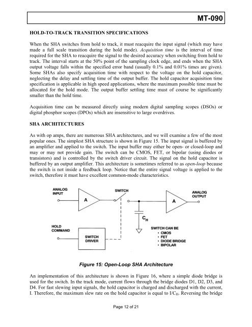
As with op amps, there are numerous SHA architectures, <strong>and</strong> we will examine a few of the most<br />
popular ones. The simplest SHA structure is shown in Figure 15. The input signal is buffered by<br />
an amplifier <strong>and</strong> applied to the switch. The input buffer may either be open- or closed-loop <strong>and</strong><br />
may or may not provide gain. The switch can be CMOS, FET, or bipolar (using diodes or<br />
transistors) <strong>and</strong> is controlled by the switch driver circuit. The signal on the hold capacitor is<br />
buffered by an output amplifier. This architecture is sometimes referred to as open-loop because<br />
the switch is not inside a feedback loop. Notice that the entire signal voltage is applied to the<br />
switch, therefore it must have excellent common-mode characteristics.<br />
Figure 15: Open-Loop SHA Architecture<br />
An implementation of this architecture is shown in Figure 16, where a simple diode bridge is<br />
used for the switch. In the track mode, current flows through the bridge diodes D1, D2, D3, <strong>and</strong><br />
D4. For fast slewing input signals, the hold capacitor is charged <strong>and</strong> discharged with the current,<br />
I. Therefore, the maximum slew rate on the hold capacitor is equal to I/CH. Reversing the bridge<br />
Page 12 of 21


