

AN-9745 Design Guide for TRIAC Dimmable LED Driver Using ...
AN-9745 Design Guide for TRIAC Dimmable LED Driver Using ...
AN-9745 Design Guide for TRIAC Dimmable LED Driver Using ...

Create successful ePaper yourself
Turn your PDF publications into a flip-book with our unique Google optimized e-Paper software.
<strong>AN</strong>-<strong>9745</strong><br />
www.fairchildsemi.com<br />
<strong>Design</strong> <strong>Guide</strong> <strong>for</strong> <strong>TRIAC</strong> <strong>Dimmable</strong> <strong>LED</strong> <strong>Driver</strong> <strong>Using</strong> FL7730<br />
Introduction<br />
An <strong>LED</strong> has become a promising light source <strong>for</strong> replacing<br />
conventional lighting systems, such as fluorescent and<br />
incandescent lights. Especially in the conventional <strong>TRIAC</strong><br />
dimmer infrastructure, there has been much research into<br />
development of an <strong>LED</strong> bulb compatible with <strong>TRIAC</strong><br />
dimmers. Because the incandescent light source consumes a<br />
hundred watt with short life time, an <strong>LED</strong> bulb can be the<br />
excellent substitute with considerably less power dissipation<br />
and longer life.<br />
The biggest recent issue of <strong>TRIAC</strong> dimmable <strong>LED</strong> bulb is<br />
dimmer compatibility. The conventional <strong>TRIAC</strong> dimmer<br />
was originally designed to handle hundreds of watts<br />
induced by incandescent bulbs. An <strong>LED</strong> bulb consuming<br />
less than 20 W should interact with those dimmers<br />
composed of high-power devices. If the interaction between<br />
dimmer and <strong>LED</strong> bulb is not stabilized, visible flicker is<br />
perceptible.<br />
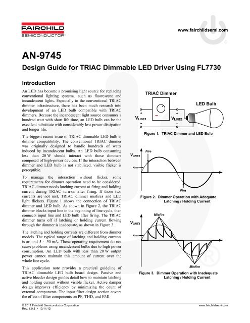
To manage the interaction without flicker, some<br />
requirements <strong>for</strong> dimmer operation need to be considered.<br />
<strong>TRIAC</strong> dimmer needs latching current at firing and holding<br />
current during <strong>TRIAC</strong> turn-on after firing. If those two<br />
currents are not met, <strong>TRIAC</strong> dimmer misfires and <strong>LED</strong><br />
light flickers. Figure 1 shows the connection of <strong>TRIAC</strong><br />
dimmer and <strong>LED</strong> bulb. As shown in Figure 2, the <strong>TRIAC</strong><br />
dimmer blocks input line in the beginning of line cycle, then<br />
connects input line and <strong>LED</strong> bulb after firing. The <strong>TRIAC</strong><br />
dimmer turns off if latching or holding current flowing<br />
through the dimmer is inadequate, as shown in Figure 3.<br />
The latching and holding currents are different from dimmer<br />
models. The typical range of latching and holding currents<br />
is around 5 ~ 50 mA. Those operating requirement do not<br />
cause problems using incandescent bulbs due to high power<br />
consumption. An <strong>LED</strong> bulb with less than 20 W output<br />
power cannot maintain this amount of current over the<br />
whole line cycle.<br />
This application note provides a practical guideline of<br />
<strong>TRIAC</strong> dimmable <strong>LED</strong> bulb board design. Passive and<br />
active bleeder design guides detail how to maintain latching<br />
and holding current without visible flicker. Active damper<br />
design improves efficiency by minimizing the count of<br />
external components. The input filter design section covers<br />
the effect of filter components on PF, THD, and EMI.<br />
Figure 1. <strong>TRIAC</strong> Dimmer and <strong>LED</strong> Bulb<br />
Figure 2. Dimmer Operation with Adequate<br />
Latching / Holding Current<br />
Figure 3. Dimmer Operation with Inadequate<br />
Latching / Holding Current<br />
© 2011 Fairchild Semiconductor Corporation www.fairchildsemi.com<br />
Rev. 1.0.2 • 10/11/12
<strong>AN</strong>-<strong>9745</strong> APPLICATION NOTE<br />
1. Passive Bleeder <strong>Design</strong><br />
The passive bleeder is designed to supply latching and<br />
holding current to eliminate misfire and flicker. Figure 4<br />
shows a board schematic using a passive bleeder.<br />
Figure 4. <strong>LED</strong> <strong>Driver</strong> Schematic with Passive Bleeder<br />
A passive bleeder is composed of a resistor (RB) and a<br />
capacitor (CB). LF1 and LF2 are input filter inductors. CIN is<br />
input filter capacitor and RD is damper resistor.<br />
In dimmable board design, a resistor (ex. RB, RD) needs to<br />
be connected in series with a capacitor (ex. CB, CIN) in case<br />
that the capacitor is located in between input lines. Without<br />
the series resistor, a large voltage and current spike occurs<br />
due to the quickly charged energy in the capacitor at<br />
dimmer firing. The current spike can damage the <strong>TRIAC</strong><br />
dimmer, especially when <strong>LED</strong> bulbs are connected in<br />
parallel with the dimmer because the sum of the current<br />
spike from each <strong>LED</strong> bulb can be over the rated current of<br />
the <strong>TRIAC</strong> dimmer. Current ringing after the current spike<br />
can also cause the <strong>TRIAC</strong> dimmer to misfire due to<br />
negative current of less than the holding current in the<br />
oscillation. The voltage spike can destroy external<br />
components if it is over the rated breakdown voltage.<br />
The passive bleeder includes a hundreds-of-nF capacitor<br />
(CB) to provide latching and holding current. To remove the<br />
voltage and current spike described above, a bleeder resistor<br />
(RB) is necessary to dampen the spike.<br />
1.1 Passive Bleeder Capacitor (CB) Selection<br />
The capacity of CB determines the bleeder current to retain<br />
<strong>TRIAC</strong> turn-on. In terms of <strong>TRIAC</strong> dimming, bigger CB has<br />
better stability in dimming control due to large bleeder<br />
current. Figure 5 and Figure 6 show the line current of small<br />
and large bleeder capacitors. The input current (IIN) is the<br />
current from the flyback converter behind the bridge diode.<br />
IIN is in-phase with line voltage by power factor correction<br />
controlled by FL7730. IB is bleeder current and line current<br />
(ILINE) is the sum of IIN and IB.<br />
Figure 5. Line Current, Small Bleeder Capacitor (C B)<br />
Figure 6. Line Current, Large Bleeder Capacitor (C B)<br />
ILINE should be higher than latching and holding current<br />
because ILINE directly flows through the <strong>TRIAC</strong> dimmer. In<br />
Figure 5, ILINE at firing is not large enough due to the small<br />
CB. The <strong>TRIAC</strong> dimmer can misfire right after firing, as<br />
shown in Figure 3. In Figure 6, ILINE is higher at dimmer<br />
firing with the large CB, which can maintain normal turn-on<br />
state of <strong>TRIAC</strong>, as shown in Figure 2. There<strong>for</strong>e, a large CB<br />
maintains dimmer firing better than a small CB by supplying<br />
higher IB.<br />
However, a large CB has a drawback in PF, THD, and<br />
efficiency. Table 1 shows the system per<strong>for</strong>mance<br />
comparison between 100 nF and 220 nF CB. CB has a<br />
significant influence on PF and power dissipation in RB.<br />
Compared to 100 nF CB, the 220 nF CB seriously drops PF<br />
and increases power dissipation of RB due to the larger<br />
charging and discharging current of CB.<br />
Table 1. CB Effect on System Per<strong>for</strong>mance<br />
TEST CONDITION: VIN = 230 VAC, POUT = 8 W, RB = 2 kΩ<br />
PF THD PD in RB<br />
C B [100 nF] 0.93 13% 162 mW<br />
C B [220 nF] 0.85 11% 684 mW<br />
There<strong>for</strong>e, <strong>TRIAC</strong> dimming control and PF require<br />
balanced trade-off when selecting CB in the passive bleeder.<br />
Especially in high-line bulb with high PF requirements;<br />
these two factors can make finding the proper CB a<br />
challenge. In the CB selection, the first step is to see IB<br />
during dimmer firing by changing CB to check if there is<br />
any misfire at dimmer firing due to inadequate IB. In the<br />
range of CB without abnormal operation in dimmer firing,<br />
choose the minimum CB <strong>for</strong> higher PF and efficiency. The<br />
EMI is not affected by CB because RB is connected in series<br />
and interrupts noise filtering by CB.<br />
© 2011 Fairchild Semiconductor Corporation www.fairchildsemi.com<br />
Rev. 1.0.2 • 10/11/12 2
<strong>AN</strong>-<strong>9745</strong> APPLICATION NOTE<br />
1.2 Passive Bleeder Resistor (RB) Selection<br />
RB is the damper <strong>for</strong> reducing the spike current caused by<br />
quick charging of CB at firing. Figure 7 shows line current<br />
with excessively large RB. Too large RB dampens IB too<br />
much and limits IB less than latching current at firing. Then,<br />
the <strong>TRIAC</strong> dimmer can misfire right after firing so that<br />
visible flicker is appears.<br />
Figure 7. Line Current with Excessively Large RB Figure 8 shows ILINE with excessively small RB. If RB is too<br />
small, RB doesn’t fully dampen the spike current and<br />
ringing current occurs. The ringing current fluctuates under<br />
the negative IB, which causes misfire of the <strong>TRIAC</strong> dimmer<br />
and visible flicker.<br />
Figure 8. Line Current with Excessively Small RB Another consideration in RB selection is power loss. Table 2<br />
compares system per<strong>for</strong>mance using two different bleeder<br />
resistors. In the system specification, RB doesn’t affect PF<br />
and THD; however, large RB makes increases power<br />
dissipation in RB.<br />
Table 2. RB Effect on System Per<strong>for</strong>mance<br />
TEST CONDITION: Vin = 230 VAC, POUT = 8 W, CB = 100 nF<br />
PF THD PD IN RB RB [1 kΩ] 0.93 13% 100 mW<br />
R B [2 kΩ] 0.93 13% 162 mW<br />
In RB selection, the excessively large and small RB values<br />
should be found first. Then, the minimum RB can be<br />
selected in the proper range of RB <strong>for</strong> better efficiency.<br />
2. Active Bleeder <strong>Design</strong><br />
Another method to maintain <strong>TRIAC</strong> holding current is<br />
active bleeding technique. The active bleeder can cover a<br />
wider range of <strong>TRIAC</strong> turn-on in a line input cycle<br />
compared to passive bleeder. The proposed active bleeder<br />
retains <strong>TRIAC</strong> holding current by regulating input current,<br />
which minimizes power loss in the bleeder circuit.<br />
Figure 9. Active Bleeder Schematic<br />
In Figure 9, ILINE is the sum of IB (active bleeder current)<br />
and IIN (flyback input current). RSENSE is sensing resistor<br />
detecting line current, ILINE. CFILTER is the filter capacitor to<br />
filter switching noise at RSENSE voltage. QREG is a shunt<br />
regulator, such as KA431. At dimmer firing, a large current<br />
spike causes a large voltage drop at RSENSE. ZDLIM limits<br />
RSENSE voltage to protect reference block of QREG. Biasing<br />
current to drive QBLEED (bleeder MOSFET) as a linear<br />
regulator is supplied by auxiliary winding. The biasing<br />
circuit consists of DBIAS and CBIAS. The gate of QBLEED is<br />
controlled by the CBIAS biasing voltage and cathode of QREG.<br />
The amount of driving current is limited by RSOURCE and<br />
RSINK. CCOMP reduces response of the regulation loop. RCOMP<br />
compensates control loop as a negative feedback resistor.<br />
© 2011 Fairchild Semiconductor Corporation www.fairchildsemi.com<br />
Rev. 1.0.2 • 10/11/12 3<br />
IB<br />
ILINE<br />
(IIN+IB)<br />
Set holding current<br />
= VREF(QREG) / RSENSE<br />
ILINE regulation<br />
Figure 10. Line Current <strong>Using</strong> Active Bleeder<br />
IIN
<strong>AN</strong>-<strong>9745</strong> APPLICATION NOTE<br />
The functional operation is shown in Figure 10. In this<br />
active bleeder, VGS (gate-source voltage) of QBLEED is<br />
increased and IB becomes higher when RSENSE voltage is less<br />
than VREF of QREG. The holding current is given as:<br />
I<br />
V<br />
( Q<br />
)<br />
REF REG<br />
HOLD � (1)<br />
RSENSE<br />
In the selection of the IHOLD, there is a trade-off between<br />
dimmer compatibility and system efficiency. If IHOLD is set<br />
high, the active bleeder is more compatible with more<br />
dimmers; but the amount of IB increases with more power<br />
dissipation in the active bleeder.<br />
RSOURCE, RSINK, CCOMP, RCOMP, and CFILTER have a close<br />
relationship with the feedback response of the active<br />
bleeder. Smaller resistance (RSOURCE, RSINK, RCOMP) and<br />
capacitance (CCOMP, CFILTER) increase the speed of the<br />
feedback loop. If feedback loop is too fast, IB oscillates with<br />
a large current ripple.<br />
The operation of the active bleeder should be synchronized<br />
with the normal IC operation period. When the IC is in an<br />
abnormal condition, such as an <strong>LED</strong> short and open, there is<br />
no IIN due to shutdown gate signal. If active bleeder is still<br />
activated in this abnormal condition, the active bleeder<br />
should maintain holding current without IIN and the power<br />
dissipation in the active bleeder is very high and QBLEED is<br />
thermally destroyed. There<strong>for</strong>e, the biasing current should<br />
come from the auxiliary winding. Then, the active bleeder<br />
can be disabled when switching is shut down.<br />
Figure 11 is a design example of an active bleeder. Probe<br />
ground is connected to VREF of the shunt regulator<br />
(KA431). C1 is the RSENSE voltage and C2 is the input<br />
voltage. C3 is the bleeder MOSFET source voltage, which<br />
is proportional to bleeder current. C4 is current probed line<br />
current.<br />
1N4003<br />
3k<br />
100n<br />
KA431<br />
C1(V_RSENSE)<br />
C4(ILINE)<br />
Aux.<br />
winding<br />
1k<br />
100/0.5W<br />
100n<br />
680n<br />
C2(VIN)<br />
FQPF2N50<br />
C3(QBLEED SOURCE)<br />
100/0.5W<br />
Probe GND<br />
3V<br />
Figure 11. Example of Active Bleeder in 8 W Bulb<br />
Figure 12. Measured Wave<strong>for</strong>m at High Dimming Angle<br />
Figure 13. Measured Wave<strong>for</strong>m at Low Dimming Angle<br />
Figure 12 and Figure 13 show the wave<strong>for</strong>ms of the active<br />
bleeder at high and low dimming angle. At low dimming<br />
angle, output current is reduced by the dimming function in<br />
FL7730. The active bleeder should compensate more IB<br />
current due to the reduced IIN (C3). That is why the power<br />
dissipation in the active bleeder is in the middle dimming<br />
angle range. To check the maximum bleeder temperature,<br />
the test condition should be a middle dimming angle and<br />
maximum line input voltage.<br />
3. Active Damper <strong>Design</strong><br />
A resistive damper is necessary in series with input filter<br />
capacitor (CIN) when <strong>TRIAC</strong> dimmer is fired. At dimmer<br />
firing, a large current spike is induced through input line to<br />
quickly charge CIN. Without the resistive damper, the large<br />
spike creates line current oscillation, causing dimmer<br />
misfire and damage to the <strong>TRIAC</strong> dimmer with the<br />
excessive current. While the damper resistor suppresses the<br />
spike current, the power loss in the damper resistor is very<br />
high. The damper resistor not only dampens the spike<br />
current, but also handles the input current from the flyback.<br />
There<strong>for</strong>e, Fairchild’s proprietary active damper is proposed<br />
to reduce the power loss with minimized external<br />
components. In Figure 14, RAD is the active damper resistor<br />
and QAD is damper MOSFET to reduce power loss of RAD.<br />
RD and CD are delay circuit components and DD is reset<br />
diode to discharge CD.<br />
© 2011 Fairchild Semiconductor Corporation www.fairchildsemi.com<br />
Rev. 1.0.2 • 10/11/12 4
<strong>AN</strong>-<strong>9745</strong> APPLICATION NOTE<br />
IIN<br />
VIN<br />
RD<br />
DD<br />
QAD<br />
RAD<br />
VAD<br />
CD<br />
VGATE<br />
CIN<br />
Figure 14. Active Damper Schematic<br />
Figure 15. Active Damper Wave<strong>for</strong>ms<br />
Single-Stage<br />
Flyback<br />
Figure 15 shows the operational wave<strong>for</strong>ms of the active<br />
damper. Mode analysis is as according to the sequence:<br />
M1: Dimmer turn-off period; QAD turns off.<br />
M2: Dimmer is fired and spike current occurs.<br />
VGATE is gradually increased by the delay circuit (RD<br />
and CD)<br />
M3: QAD turns on by the charged VGATE.<br />
VAD is regulated as VTH of QAD.<br />
M4: CD is discharged by DD and VGATE is reset <strong>for</strong> the<br />
next line cycle. The discharging current path is<br />
DD - RAD - CD.<br />
During M3 period, QAD can considerably reduce power loss<br />
in RAD by regulating VAD as its threshold voltage (VTH).<br />
Table 3 shows power dissipation of passive and active<br />
dampers. The power loss of active damper is much lower<br />
than passive damper resistor. At low line (110 VAC), input<br />
current is high and the damper resistor handles the large<br />
current. There<strong>for</strong>e, the active damper is strongly<br />
recommended at low line model.<br />
Table 3. Passive vs. Active Damper Power Loss<br />
POUT = 8W<br />
Damper Power<br />
Dissipation [mW]<br />
VIN: 110 VAC VIN: 220 VAC PASSIVE DAMPER, 200 Ω 1200 290<br />
ACTIVE DAMPER, 200 Ω +<br />
FQN1N50C (V TH: 2~4 V)<br />
ACTIVE DAMPER, 200 Ω +<br />
FDD10N20LZ (V TH: 1~2.5 V)<br />
278 161<br />
171 113<br />
3.1 Active Damper Resistor (RAD) Selection<br />
A voltage and current spike should be checked first when<br />
selecting RAD. Voltage spikes can damage the MOSFET and<br />
filter capacitor over the rated voltage. Current spikes create<br />
current ringing at dimmer firing. As shown in Figure 16, IIN<br />
ringing occurs at firing with small RAD. This ringing current<br />
drops IIN and the lowered IIN can lead to misfire of the<br />
dimmer and visible flicker. Also, a large peak current spike<br />
by using small RAD might damage the <strong>TRIAC</strong> dimmer,<br />
especially when the dimming <strong>LED</strong> bulbs are connected in<br />
parallel. There<strong>for</strong>e, check points when selecting RAD are:<br />
� Voltage spike (should be less than the part’s breakdown<br />
voltage.)<br />
� Current spike (should be less than the <strong>TRIAC</strong> dimmer’s<br />
rated current. If considering connecting bulbs in<br />
parallel, the current spike should be lower inversely<br />
proportional to the number of <strong>LED</strong> bulbs.)<br />
� Current ringing (check the dropped IIN at firing if it is<br />
enough higher than <strong>TRIAC</strong> holding current.)<br />
After checking the above considerations, choose the<br />
minimum RAD to maximize efficiency.<br />
Figure 16. V IN and I IN with Small Damper Resistor (R AD)<br />
3.2 Active Damper MOSFET (QAD) Selection<br />
The maximum VAD should be less than the breakdown<br />
voltage of QAD. After selecting RAD, maximum VAD can be<br />
checked at 90º dimming angle and the highest input line<br />
© 2011 Fairchild Semiconductor Corporation www.fairchildsemi.com<br />
Rev. 1.0.2 • 10/11/12 5
<strong>AN</strong>-<strong>9745</strong> APPLICATION NOTE<br />
voltage. Then, choose proper QAD with breakdown voltage<br />
margin. 1~2 A current rating is enough in the 8W <strong>LED</strong><br />
bulb. As shown in Table 3, logic-level MOSFET with low<br />
threshold voltage can additionally reduce power loss<br />
because the regulated VAD is QAD threshold voltage.<br />
3.3 Active Damper Diode (DD) Selection<br />
The active damper diode discharges CD to reset VGATE.<br />
Diode with 1A rated <strong>for</strong>ward current is enough to discharge<br />
CD. Same as the QAD selection, maximum VAD at 90°<br />
dimming angle and the highest input line voltage should be<br />
checked first to select DD reverse voltage specification.<br />
3.4 Active Damper Delay Circuit (RD, CD)<br />
Selection<br />
The delay circuit (RD, CD) should create a long enough<br />
delay time be<strong>for</strong>e QAD turns on to let RAD dampen the<br />
current spike. The worst case <strong>for</strong> the spike current is 90°<br />
dimming angle. Spike current ringing needs to be checked<br />
first at 90° dimming angle to determine how long the spike<br />
current is dampened. Then, adjust RD and CD to guarantee<br />
the dampened period. The recommended CD and RD values<br />
are hundreds of nF and tens of kΩ. If CD is too large and RD<br />
is very small, DD cannot fully discharge CD in M4, as shown<br />
in Figure 15.<br />
<strong>Design</strong> Example<br />
Figure 17 shows the design example of the active damper in<br />
an 8W <strong>LED</strong> bulb system. As shown in Figure 18 and Figure<br />
19, the delay by 80 kΩ RD and 100 nF CD is around 1ms.<br />
During the delay, 220 Ω RAD dampens voltage and current<br />
spike without current ringing or dimmer misfire.<br />
© 2011 Fairchild Semiconductor Corporation www.fairchildsemi.com<br />
Rev. 1.0.2 • 10/11/12 6<br />
IIN<br />
VIN<br />
80k 100nF<br />
ES1J<br />
FQN1N50C<br />
VAD<br />
220/1W<br />
VGATE<br />
Figure 17. <strong>Design</strong> Example: Active Damper in 8W Bulb<br />
Figure 18. Measured Wave<strong>for</strong>m at High Dimming Angle<br />
Figure 19. Measured Wave<strong>for</strong>m at Low Dimming Angle<br />
CIN
<strong>AN</strong>-<strong>9745</strong> APPLICATION NOTE<br />
4. Features of FL7730<br />
The FL7730 is an active power factor correction (PFC)<br />
controller using single-stage flyback topology. Dimming<br />
control with no flicker is implemented by the analog<br />
sensing method. Primary-side regulation and single-stage<br />
topology reduce external components, such as input bulk<br />
capacitor and feedback circuitry to minimize cost. To<br />
improve power factor and THD, constant on-time control is<br />
utilized with an internal error amplifier and low bandwidth<br />
compensator. Precise constant-current control regulates<br />
accurate output current, independent of input voltage and<br />
output voltage. Operating frequency is proportionally<br />
adjusted by output voltage to guarantee DCM operation<br />
with higher efficiency and simpler design. FL7730 provides<br />
protections such as open-<strong>LED</strong>, short-<strong>LED</strong>, and overtemperature<br />
protection.<br />
Table 4. Pin Definitions<br />
Pin # Name Description<br />
1 CS<br />
Figure 20. Package Diagram<br />
Current Sense. This pin connects a current-sense resistor to detect the MOSFET current <strong>for</strong> the<br />
output-current regulation in constant-current regulation.<br />
2 GATE PWM Signal Output. This pin uses the internal totem-pole output driver to drive the power MOSFET.<br />
3 GND Ground<br />
4 VDD Power Supply. IC operating current and MOSFET driving current are supplied using this pin.<br />
5 DIM Dimming. This pin controls the dimming operation of the <strong>LED</strong> lighting.<br />
6 VS<br />
Voltage Sense. This pin detects the output voltage in<strong>for</strong>mation and discharge time <strong>for</strong> linear frequency<br />
control and constant-current regulation. This pin connects divider resistors from the auxiliary winding.<br />
7 COMI Constant-Current Loop Compensation. This pin is the output of the transconductance error amplifier.<br />
8 GND Ground<br />
Figure 21. Functional Block Diagram<br />
© 2011 Fairchild Semiconductor Corporation www.fairchildsemi.com<br />
Rev. 1.0.2 • 10/11/12 7
<strong>AN</strong>-<strong>9745</strong> APPLICATION NOTE<br />
<strong>Design</strong> Summary<br />
Figure 22 shows the schematic of the <strong>TRIAC</strong> dimmable <strong>LED</strong> driver using FL7730. This schematic is dedicated to low-line<br />
voltage (90~140 VAC).<br />
L1<br />
4.7mH<br />
R1<br />
560/0.5W<br />
C1<br />
330n<br />
F1<br />
1A/250V<br />
Q1<br />
MB8S<br />
C3<br />
100nF<br />
R8<br />
150k<br />
R9<br />
20k<br />
R3<br />
20k<br />
R2<br />
100/0.5W<br />
L2<br />
4.7mH<br />
D1<br />
C2<br />
ES1J<br />
330n<br />
Q2<br />
FQN1N50C<br />
D2 11V<br />
R6 62k<br />
R4<br />
1M<br />
R5<br />
75k<br />
R10<br />
100kΩ<br />
0.5W<br />
N1 N3<br />
© 2011 Fairchild Semiconductor Corporation www.fairchildsemi.com<br />
Rev. 1.0.2 • 10/11/12 8<br />
R11<br />
510k<br />
D3<br />
1N4003<br />
R12<br />
510k<br />
C8<br />
10n<br />
D4<br />
RS1M<br />
R7<br />
0<br />
Q3 FL7730<br />
C7<br />
N2<br />
C5<br />
10p<br />
C4 3.3u<br />
C6<br />
2.2u<br />
5<br />
Dim<br />
6<br />
VS<br />
7<br />
COMI<br />
8<br />
N.C<br />
VDD<br />
GND<br />
GATE<br />
CS<br />
4<br />
3<br />
2<br />
1<br />
47u<br />
R16<br />
200Ω<br />
R13<br />
10Ω<br />
Q4<br />
FQU5N60C<br />
C9<br />
4.7nF<br />
R14<br />
1.2Ω<br />
R15<br />
1.0Ω<br />
D5<br />
ES3D<br />
C10<br />
35V/330uF<br />
Figure 22. Schematic of <strong>TRIAC</strong> <strong>Dimmable</strong> <strong>LED</strong> <strong>Driver</strong> <strong>Using</strong> FL7730 (Low Line: 90~140 V AC)<br />
NP2(3 4)<br />
NA(2 6)<br />
NP1(5 3)<br />
Figure 23. Trans<strong>for</strong>mer Structure<br />
C11<br />
35V/1000uF<br />
NS<br />
(NS- NS+)<br />
Table 5. Winding Specifications<br />
No Winding Pin (S → F) Wire Turns Winding Method<br />
1 NP1 5 � 3 0.13φ 38 Ts Solenoid Winding<br />
2 Insulation: Polyester Tape t = 0.025 mm, 2-Layer<br />
3 NS NS- � NS+ 0.3φ (TIW) 24 Ts Solenoid Winding<br />
4 Insulation: Polyester Tape t = 0.025 mm, 2-Layer<br />
5 NA 2 � 6 0.13φ 18 Ts Solenoid Winding<br />
6 Insulation: Polyester Tape t = 0.025 mm, 2-Layer<br />
7 NP2 3 � 4 0.13φ 38 Ts Solenoid Winding<br />
8 Insulation: Polyester Tape t = 0.025 mm, 6-Layer<br />
Table 6. Electrical Characteristics<br />
Pin Specification Remark<br />
Inductance 1 – 2 1 mH ±10% 50 kHz, 1 V<br />
Leakage 1 – 2 8 µH 50kHz, 1 V Short All Output Pins<br />
VO<br />
R17<br />
51k
<strong>AN</strong>-<strong>9745</strong> APPLICATION NOTE<br />
Experimental Verification<br />
The design example with passive bleeder and active damper<br />
was experimentally verified in an 8 W <strong>LED</strong> lighting system.<br />
Figure 24 shows constant current regulation at input voltage<br />
and output voltage change. Constant-current deviation in<br />
the wide output voltage range from 10 V to 28 V is less than<br />
2.1% at each line input voltage. Line regulation at the rated<br />
output voltage (22 V) is less than 3.9%.<br />
Operation wave<strong>for</strong>ms are shown in Figure 25, Figure 26,<br />
and Figure 27. In this dimmable board, <strong>TRIAC</strong> dimmer<br />
firing is stabilized without any misfire. FL7730 keeps<br />
constant tON so VCS is in phase with VIN. The maximum<br />
spike current of IIN is 1.2 A. Figure 28 shows the dimming<br />
curve. RMS input voltage indicates <strong>TRIAC</strong> dimming angle.<br />
<strong>LED</strong> current is smoothly controlled by the FL7730 dimming<br />
function and external circuits, such as the passive bleeder<br />
and active damper. Table 7 provides compatibility with<br />
common dimmers <strong>for</strong> a design without visible flicker.<br />
Maximum and minimum current vary because each<br />
dimmer’s maximum and minimum angles are different.<br />
System efficiency is from 80.7% to 82.9% at low line input<br />
voltage (90 ~ 140 VAC). The active damper helps improve<br />
the efficiency with a compact and inexpensive design<br />
solution. Table 8 shows PF and THD in a low line input<br />
voltage range of 90~140 VAC. PF is over 0.9 and THD is<br />
much less than 30% by constant tON and linear frequency<br />
control in the FL7730.<br />
The per<strong>for</strong>mances obtained in the design example show a<br />
powerful <strong>LED</strong> lighting solution with accurate constant<br />
current regulation, stable dimming control, high efficiency,<br />
high PF, and low THD with low BOM cost.<br />
IOUT [mA]<br />
OVP<br />
Figure 24. CC Regulation, Measured by CR-Load<br />
Figure 25. Wave<strong>for</strong>ms at Maximum Dimming Angle<br />
© 2011 Fairchild Semiconductor Corporation www.fairchildsemi.com<br />
Rev. 1.0.2 • 10/11/12 9<br />
IIN<br />
VIN<br />
VCS<br />
Figure 26. Wave<strong>for</strong>ms at Half Dimming Angle<br />
IIN<br />
VIN<br />
VCS<br />
Figure 27. Wave<strong>for</strong>ms at Minimum Dimming Angle
<strong>AN</strong>-<strong>9745</strong> APPLICATION NOTE<br />
Table 7. Dimmer Compatibility<br />
Manufacturer Dimmer Maximum Current Minimum Current Flicker<br />
LUTRON S-600P-WH 330 mA 40 mA (12%) No<br />
LUTRON CN-600P-WH 328 mA 11 mA (3.4%) No<br />
LUTRON GL-600H 365 mA 8 mA (2.2%) No<br />
LUTRON TG-603PGH-WH 252 mA 12 mA (4.8%) No<br />
LUTRON TG-600PH-WH 333 mA 14 mA (4.2%) No<br />
LUTRON LG-600P 327 mA 3 mA (0.9%) No<br />
LUTRON CTCL-153PD 320 mA 58 mA (18%) No<br />
LEVITON IP106 380 mA 36 mA (9.5%) No<br />
LEVITON 1C4005 344 mA 0 mA (0%) No<br />
LEVITON 6631-LW 340 mA 0 mA (0%) No<br />
Legrand F 165H 344 mA 3 mA (0.9%) No<br />
Figure 28. Dimming Curve (Input Voltage vs.<br />
<strong>LED</strong> Current)<br />
Figure 29. Efficiency<br />
Table 8. Power Factor (PF) and Total Harmonic Distortion (THD)<br />
Input Voltage Output Current Output Voltage PF THD<br />
90 VAC 360 mA 21.70 V 0.98 7.4%<br />
110 VAC 376 mA 21.77 V 0.96 9.5%<br />
120 VAC 380 mA 21.77 V 0.95 10.4%<br />
140 VAC 386 mA 21.79 V 0.91 12.4%<br />
© 2011 Fairchild Semiconductor Corporation www.fairchildsemi.com<br />
Rev. 1.0.2 • 10/11/12 10
<strong>AN</strong>-<strong>9745</strong> APPLICATION NOTE<br />
Related Datasheets<br />
FL7730MY — Single-Stage Primary-Side-Regulation PWM Controller <strong>for</strong> PFC and <strong>LED</strong> <strong>Dimmable</strong> Driving<br />
KA431 — Programmable Shunt Regulator<br />
DISCLAIMER<br />
FAIRCHILD SEMICONDUCTOR RESERVES THE RIGHT TO MAKE CH<strong>AN</strong>GES WITHOUT FURTHER NOTICE TO <strong>AN</strong>Y PRODUCTS<br />
HEREIN TO IMPROVE RELIABILITY, FUNCTION, OR DESIGN. FAIRCHILD DOES NOT ASSUME <strong>AN</strong>Y LIABILITY ARISING OUT OF THE<br />
APPLICATION OR USE OF <strong>AN</strong>Y PRODUCT OR CIRCUIT DESCRIBED HEREIN; NEITHER DOES IT CONVEY <strong>AN</strong>Y LICENSE UNDER ITS<br />
PATENT RIGHTS, NOR THE RIGHTS OF OTHERS.<br />
LIFE SUPPORT POLICY<br />
FAIRCHILD’S PRODUCTS ARE NOT AUTHORIZED FOR USE AS CRITICAL COMPONENTS IN LIFE SUPPORT DEVICES OR SYSTEMS<br />
WITHOUT THE EXPRESS WRITTEN APPROVAL OF THE PRESIDENT OF FAIRCHILD SEMICONDUCTOR CORPORATION.<br />
As used herein:<br />
1. Life support devices or systems are devices or systems<br />
which, (a) are intended <strong>for</strong> surgical implant into the body, or<br />
(b) support or sustain life, or (c) whose failure to per<strong>for</strong>m<br />
when properly used in accordance with instructions <strong>for</strong> use<br />
provided in the labeling, can be reasonably expected to<br />
result in significant injury to the user.<br />
2. A critical component is any component of a life support<br />
device or system whose failure to per<strong>for</strong>m can be reasonably<br />
expected to cause the failure of the life support device or<br />
system, or to affect its safety or effectiveness.<br />
© 2011 Fairchild Semiconductor Corporation www.fairchildsemi.com<br />
Rev. 1.0.2 • 10/11/12 11


