Design of High Frequency Ultrasound Transducers using ...
Design of High Frequency Ultrasound Transducers using ...
Design of High Frequency Ultrasound Transducers using ...

Create successful ePaper yourself
Turn your PDF publications into a flip-book with our unique Google optimized e-Paper software.
<strong>Design</strong> <strong>of</strong> <strong>High</strong> <strong>Frequency</strong> <strong>Ultrasound</strong> <strong>Transducers</strong> <strong>using</strong><br />
Micromachining<br />
Tung Manh, Anh Tuan. T. Nguyen, Lars H<strong>of</strong>f and Tonni F.Johansen<br />
Abstract— We present a new design <strong>of</strong> high frequency<br />
ultrasound transducers <strong>using</strong> thick-film PZT on Silicon for<br />
medical application. Air is used as backing material for the<br />
PZT film, and the ultrasound pulses are transmitted through<br />
the silicon substrate. The silicon substrate is micromachined to<br />
build acoustic matching layers to optimize the acoustic coupling<br />
between the active PZT layer and the tissue, and achieve a<br />
large bandwidth. The number <strong>of</strong> matching layers in the design<br />
could be either two or three, depending on the fabrication<br />
methods to make the PZT thick-film, i.e. tape casting or screen<br />
printing. A prototype <strong>of</strong> two matching layers for a 10MHz<br />
transducer has been made. 1D analytical calculations and FEM<br />
simulations show that the proposed design will have a 3 dB<br />
bandwidth ranging from 7.5 MHz to 13 MHz, or 55%<br />
bandwidth at center frequency <strong>of</strong> 10 MHz. Acoustic<br />
measurement is ongoing.<br />
I. INTRODUCTION<br />
H IGH frequency ultrasound transducers are wanted in<br />
medical imaging applications where high resolution is<br />
needed [1]-[2]. Most <strong>of</strong> today’s medical ultrasound<br />
transducers are based on an active ceramic layer <strong>of</strong> lead<br />
zirconate titanate (PZT) vibrating in thickness mode. To<br />
achieve frequencies in the range 10 to 100 MHz, the<br />
thickness <strong>of</strong> the active ceramic layer must be between 20<br />
and 200µm. Such a thin layer is difficult to lap down to a<br />
correct thickness, whereas too thick to build up by thin film<br />
techniques. In this paper, we propose <strong>using</strong> thick-film<br />
technology and silicon micromachining as fabrication<br />
technologies to bridge this gap.<br />
Previous work in this field includes Zang et al. [1], who<br />
fabricated a high frequency ultrasound transducer <strong>using</strong> PZT<br />
thick-film on a Silicon (Si) substrate, which can be annealed<br />
to a temperature <strong>of</strong> 750 0 C without reaction between the PZT<br />
film and the Si substrate. This improved the film properties<br />
compared to the previous work by Lukacs et al. [2], who<br />
used Aluminum (Al) substrate. In both <strong>of</strong> these works, the<br />
Manuscript received April 01, 2010. This work is funded by the<br />
Research Council <strong>of</strong> Norway under Grant No. 176540.<br />
Tung Manh, Anh Tuan T. Nguyen and Lars H<strong>of</strong>f are with the Faculty <strong>of</strong><br />
Science and Engineering, Vestfold University College, P.O. Box 2243, N-<br />
3103 Tønsberg, Norway (e-mail: tung.manh@ hive.no).<br />
Tonni Franke Johansen is with the Department <strong>of</strong> Circulation and<br />
Medical Imaging, University <strong>of</strong> Science and Technology, Trondheim,<br />
Norway.<br />
substrates served as temporary layers, and were etched <strong>of</strong>f to<br />
form epoxy backed transducers. This enhanced the<br />
bandwidth <strong>of</strong> the transducers, but reduced the sensitivity.<br />
We present a new design for an ultrasound transducer<br />
where substrate is kept. Using Silicon micromachining<br />
technology, the substrate is machined to form layers with<br />
descending characteristic acoustic impedance from the PZT<br />
film to the load material. These layers function as acoustic<br />
matching between the thick-film and the load. The back side<br />
<strong>of</strong> the thick-film is air, serving as the transducer backing.<br />
This structure increases sensitivity and avoids problems with<br />
reverberations in the backing material.<br />
The paper contains a description <strong>of</strong> the design transducers<br />
with details <strong>of</strong> the fabrication process to form matching<br />
layers. Details <strong>of</strong> fabrication steps to build the entire<br />
transducer can be found elsewhere [3]. The performance <strong>of</strong><br />
the designs is described analytically <strong>using</strong> the Mason stack<br />
model [4]. Finite Element Method (FEM) simulations are<br />
included to improve and verify the analytical 1D calculation.<br />
II. DESCRIPTION OF THE TRANSDUCER<br />
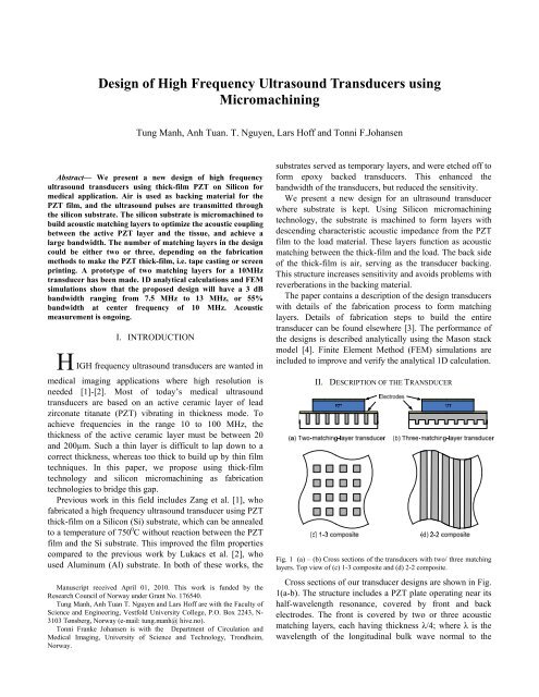
Fig. 1 (a) – (b) Cross sections <strong>of</strong> the transducers with two/ three matching<br />
layers. Top view <strong>of</strong> (c) 1-3 composite and (d) 2-2 composite.<br />
Cross sections <strong>of</strong> our transducer designs are shown in Fig.<br />
1(a-b). The structure includes a PZT plate operating near its<br />
half-wavelength resonance, covered by front and back<br />
electrodes. The front is covered by two or three acoustic<br />
matching layers, each having thickness λ/4; where λ is the<br />
wavelength <strong>of</strong> the longitudinal bulk wave normal to the
layer, at the centre frequency <strong>of</strong> the transducer. For two<br />
matching layers design [Fig. 1(a)], these two layers are: 1) a<br />
layer consisting <strong>of</strong> a composite between Si and a polymer,<br />
and 2) a layer <strong>of</strong> polymer. For three matching layers design<br />
[Fig. 1(b)], the three layers are: 1) a substrate layer <strong>of</strong> Si, 2)<br />
a composite layer between polymer and Silicon and 3) a<br />
polymer layer. Since tape-casting method gives the<br />
properties <strong>of</strong> PZT plate similar to bulk ceramic [5], the three<br />
matching layers approach should be used. In contrast, the<br />
screen printing method with sol-gel mixture provides a film<br />
with acoustic impedance approximately equal to that <strong>of</strong><br />
Silicon, two matching layers must be used.<br />
The composite layer is made as either 1-3 connectivity<br />
[Fig. 1(c)] or 2-2 connectivity type [Fig. 1(d)] <strong>using</strong><br />
micromachining techniques [6]. The 1-3 type is preferred for<br />
high frequencies (>20MHz) due to the fact <strong>of</strong><br />
manufacturing. The two electrodes function as the electric<br />
port to connect the transducer to the electronics. They<br />
should be made sufficiently thin so that their influence on<br />
the acoustic performance <strong>of</strong> the transducer is small.<br />
However, the electrodes must also be adequately thick and<br />
dense to block the diffusion between Si substrate and the<br />
thick-film [7]. An appropriate thickness is less than λ/10,<br />
where λ is the wavelength <strong>of</strong> the longitudinal bulk wave in<br />
the PZT plate.<br />
The transducer is constructed as either a single circular<br />
element or an annular array with ring elements for foc<strong>using</strong>.<br />
Scanning for image formation will be done mechanically by<br />
rotation and/or translation.<br />
III. ANALYTICAL AND FEM SIMULATIONS<br />
A. Analytical simulation<br />
The performance <strong>of</strong> the designs was modelled analytically<br />
<strong>using</strong> the Mason equivalent circuit model. In this model,<br />
PZT ceramic <strong>of</strong> type pz27 is used as the active layer, the<br />
substrate is -oriented Si, the electrodes are <strong>of</strong> Pt and<br />
the polymer is epoxy resin. A water-like medium with<br />
acoustic impedance 1.6 Mrayl is used as load. The material<br />
parameters used in the modelling are listed in TABLE I.<br />
As demonstration, only simulation corresponding to the<br />
design with two matching layer transducer at the centre<br />
frequency <strong>of</strong> 10MHz <strong>using</strong> 2-2 composite type as matching<br />
layer is performed. Fabrication <strong>of</strong> such a layer is given in<br />
IV. The second design can be found in [3].<br />
In the 10MHz transducer design, the thickness <strong>of</strong> the PZT<br />
plate is 177 µm, corresponding to λ/2 at frequency 11MHz,<br />
covered by two Pt electrodes with thickness <strong>of</strong> 3.0 µm and<br />
acoustic impedance <strong>of</strong> 84.7 Mrayls. The first matching layer<br />
is composite <strong>of</strong> Si and epoxy with thickness <strong>of</strong> 152µm and<br />
acoustic impedance <strong>of</strong> 8.9 Mrayls, whereas the last matching<br />
layer is 63µm thick epoxy with acoustic impedance <strong>of</strong><br />
2.85Mrayl [Ep<strong>of</strong>ix (Struers, Solilull, UK)]. This epoxy has<br />
acoustic impedance higher than the optimal value <strong>of</strong><br />
2.3Mrayl but was chosen due to its availability in our lab.<br />
The effective elastic parameters <strong>of</strong> the composite<br />
Si/Epoxy matching layer can be calculated <strong>using</strong> the<br />
theoretical model developed by Smith et al. [8], with some<br />
modifications. The resulting parameters are<br />
2<br />
⎡ p S<br />
2(<br />
c12 −c<br />
) ⎤<br />
S 13<br />
p<br />
c33 = v⎢c11 −( 1− v) ⎥+<br />
( 1−v)<br />
c11<br />
(a)<br />
S S p p<br />
⎢ ( 1−<br />
v)( c11 + c12 ) + v( c11+ c12)<br />
⎥<br />
⎣ ⎦<br />
p S<br />
2<br />
⎡ ( c12 −c13<br />
) ⎤<br />
S p<br />
c33 = v⎢c11−( 1− v) ⎥+<br />
( 1−v<br />
S p ) c11<br />
(b)<br />
⎢ ( 1−<br />
vc ) 11 + vc⎥<br />
11<br />
⎣ ⎦<br />
S p<br />
ρ = vρ + ( 1−v)<br />
ρ<br />
Z = c ρ<br />
c33<br />
V =<br />
ρ<br />
where the overbars ( x ) refer to effective parameters <strong>of</strong> the<br />
composite, superscript p refer to parameters <strong>of</strong> the polymer,<br />
and superscript S to parameters <strong>of</strong> the silicon substrate.<br />
cij are the elastic coefficients, ρ is the density, v is the<br />
volume fraction <strong>of</strong> Si in the composite; Z , V are the<br />
effective acoustic impedance and longitudinal wave speed in<br />
the thickness direction <strong>of</strong> the composite, respectively. (a) is<br />
the equation used for 1-3 composite whereas (b) is for 2-2<br />
type. The others are for both.<br />
The electro-acoustic transfer function, i.e. the transfer<br />
function from the voltage over the electrodes to the pressure<br />
at the transducer surface, is calculated for a 10MHz design<br />
and plotted in Fig. 2. The upper graph shows the frequency<br />
response, while the lower shows the impulse response, in the<br />
time domain. These results give an effective 3-dB bandwidth<br />
from 7.5 MHz to 13 MHz with centre frequency 10 MHz,<br />
i.e. 55% relative bandwidth.<br />
B. FEM simulation<br />
Analytical model, based on the Mason equivalent circuit,<br />
is well established in transducer modelling for describing<br />
thickness mode vibrations. However, it is limited by being a<br />
1D model. Hence, the composite layer must be described as<br />
one material with a set <strong>of</strong> calculated effective parameters,<br />
the anisotropic nature <strong>of</strong> Si is not handled, and lateral modes<br />
as well as effects <strong>of</strong> a finite width are not included.<br />
Fig. 2 Electro-acoustic transfer function and output waveform <strong>of</strong> 10MHz<br />
transducer<br />
33
Fig. 3 Electrical impedance <strong>of</strong> a 10MHz transducer<br />
To obtain more realistic simulations, and to get an<br />
estimate <strong>of</strong> the performance and limitations <strong>of</strong> the 1D<br />
analytical model, FEM models were created <strong>using</strong><br />
COMSOL Multiphysics s<strong>of</strong>tware version 3.4 (Comsol AB,<br />
Stockholm, Sweden). In FEM model, the anisotropic nature<br />
<strong>of</strong> Si is included, and the composite is made between Si and<br />
Epoxy posts. One half <strong>of</strong> a composite unit cell was modeled<br />
for 2-2 composite, whereas a quarter <strong>of</strong> cell was modeled for<br />
1-3 type. Symmetry boundary conditions were applied, as<br />
described in [9]. The sizes <strong>of</strong> the Si and polymer bars in the<br />
composite layer <strong>of</strong> the 10MHz transducer were designed to<br />
be 9µm and 23µm, respectively, to avoid interference from<br />
the lateral resonances into the thickness mode [10]. There is<br />
a good agreement between FEM simulation and analytical<br />
calculation (Fig.3). For 3 matching layer design, similar<br />
result is also achieved.<br />
IV. FABRICATION OF THE MATCHING LAYERS<br />
The novel and most important part in the transducer is the<br />
micromachined matching layer. This layer has been<br />
fabricated by <strong>using</strong> anisotropic wet etching method to form<br />
deep vertical trenches (2-2 type) into Silicon wafers,<br />
followed by vacuum impregnated these grooves by epoxy<br />
resin.<br />
The process starts with a 550 µm thick oriented Si<br />
wafer. A 1µm thin SiO2 was grown on the surfaces <strong>of</strong> the<br />
wafer. The main flat <strong>of</strong> the wafer is supposed to be<br />
parallel to the planes. However, the accuracy <strong>of</strong> this<br />
flat is approximately 1 0 , which is not efficient to have good<br />
alignment for our purposes. A two steps etching process<br />
therefore has been made. First, a mask with fan structures <strong>of</strong><br />
0.1 0 increasing step was transfer to the SiO2 layer by<br />
lithography. A 1.5 hours etch in KOH 25% at 80 0 C was then<br />
performed. All lines which are imprecisely aligned along<br />
planes were undercut and destroyed due to the nature<br />
<strong>of</strong> anisotropic wet etching. Remain lines were used to be the<br />
alignment marks for the next lithography. Fig. 4(a) shows<br />
the fan structure patterns on the plastic mask whereas the<br />
etched structures on Silicon after the first wet etching step<br />
are showed in Fig. 4(b). Due to anisotropic etching <strong>of</strong> the<br />
Silicon crystal, the circle on the mask turned to be hexagonal<br />
shape and only lines which are precisely aligned along<br />
planes have been survived completely.<br />
The grating pattern, i.e. 2-2 composite, was then<br />
transferred to the protected SiO2 layer, followed by<br />
anisotropic wet etching <strong>of</strong> the wafer for 1.5 hours to form<br />
deep trenches. A closed look <strong>of</strong> the etched structure before<br />
polymer filled is shown in Fig. 5. Obviously, straight walls<br />
have been achieved but there are steeps at the bottom <strong>of</strong> the<br />
trenches due to anisotropic behaviour <strong>of</strong> Silicon crystal.<br />
Then, the wafer was vacuum impregnated by polymer. It<br />
was done by placing the wafer into a vacuum chamber and<br />
pouring epoxy resin onto wafer’s surface. By applying a<br />
vacuum, small air bubbles in polymer were removed. The<br />
polymer was cured at room temperature for 24 hours. The<br />
sample after vacuum impregnated and cured is shown in Fig.<br />
6, where bright is Si and grey is polymer. It is clearly shown<br />
that air bubbles are removed in polymer.<br />
The sample was then lapped down to the desired<br />
thickness <strong>using</strong> a precise lapping machine (MultiPrep TM<br />
System, Allied <strong>High</strong> Tech Products Inc, USA). A PZT active<br />
layer was then glued on the sample for characterization.<br />
Characterization <strong>of</strong> these matching layers is ongoing.<br />
Fig. 4 (a) Fan structures on the glass mask (b) Patterns on Silicon wafer<br />
after the first step in Silicon wet etching process<br />
Fig. 5 Closed look <strong>of</strong> the etched structure before filled in with polymer
Fig. 6 Sample after polymer filled, bright is Silicon and grey is Polymer<br />
V. CONCLUSION<br />
The novel design <strong>of</strong> ultrasound transducers based on<br />
micromachining has been presented. A test prototype <strong>of</strong> the<br />
composite layers <strong>using</strong> wet etching has been made.<br />
Theoretical and FEM simulation show that transducers <strong>using</strong><br />
this structure to be matching layers provide 55% relative<br />
bandwidth. This is a little smaller than the optimal<br />
bandwidth that can be achieved with two matching layers<br />
but it is still reasonable. This is because we didn’t use epoxy<br />
with optimal acoustic impedance. Acoustic measurement <strong>of</strong><br />
this structure is ongoing.<br />
Active<br />
layer<br />
Passive<br />
layers<br />
Pz27<br />
[110]oriented<br />
Silicon<br />
Platinum<br />
Epoxy<br />
TABLE I<br />
MATERIAL PROPERTIES USED FOR SIMULATIONS<br />
REFERENCES<br />
[1] Q.Q. Zhang, F.T. Djuth, Q.F. Zou, C,H. Hu, J.H. Cha, K.K. Shung,<br />
“<strong>High</strong> frequency broadband PZT thick film ultrasonic transducers for<br />
medical imaging applications”.Ultrasonics, vol.44, p711-715, 2006.<br />
[2] M. Lukacs, M. Sayer, F.S. Foster, ”Single element high frequency<br />
(