Graphene plasmonics for tunable terahertz metamaterials - Physics
Graphene plasmonics for tunable terahertz metamaterials - Physics
Graphene plasmonics for tunable terahertz metamaterials - Physics

Create successful ePaper yourself
Turn your PDF publications into a flip-book with our unique Google optimized e-Paper software.
LETTERS<br />
PUBLISHED ONLINE: 4 SEPTEMBER 2011 | DOI: 10.1038/NNANO.2011.146<br />
<strong>Graphene</strong> <strong>plasmonics</strong> <strong>for</strong> <strong>tunable</strong> <strong>terahertz</strong><br />
<strong>metamaterials</strong><br />
Long Ju 1 ,BaisongGeng 1,6 , Jason Horng 1 , Caglar Girit 1 , Michael Martin 2 ,ZhaoHao 2,3 ,HansA.Bechtel 2 ,<br />
Xiaogan Liang 4 , Alex Zettl 1,5 ,Y.RonShen 1,5 and Feng Wang 1,5 *<br />
Plasmons describe collective oscillations of electrons. They have a<br />
fundamental role in the dynamic responses of electron systems<br />
and <strong>for</strong>m the basis of research into optical <strong>metamaterials</strong> 1–3 .<br />
Plasmons of two-dimensional massless electrons, as present in<br />
graphene, show unusual behaviour 4–7 that enables new <strong>tunable</strong><br />
plasmonic <strong>metamaterials</strong> 8–10 and, potentially, optoelectronic<br />
applications in the <strong>terahertz</strong> frequency range 8,9,11,12 . Here we<br />
explore plasmon excitations in engineered graphene microribbon<br />
arrays. We demonstrate that graphene plasmon resonances<br />
can be tuned over a broad <strong>terahertz</strong> frequency range by changing<br />
micro-ribbon width and in situ electrostatic doping. The ribbon<br />
width and carrier doping dependences of graphene plasmon<br />
frequency demonstrate power-law behaviour characteristic of<br />
two-dimensional massless Dirac electrons 4–6 . The plasmon<br />
resonances have remarkably large oscillator strengths, resulting<br />
in prominent room-temperature optical absorption peaks. In<br />
comparison, plasmon absorption in a conventional two-dimensional<br />
electron gas was observed only at 4.2 K (refs 13,14). The<br />
results represent afirst look at light–plasmon coupling in graphene<br />
and point to potential graphene-based <strong>terahertz</strong> <strong>metamaterials</strong>.<br />
<strong>Graphene</strong> is an attractive two-dimensional (2D) carbon material.<br />
Electrons in graphene behave like massless Dirac fermions and<br />
exhibit many exotic physical phenomena, ranging from an anomalous<br />
quantum Hall effect 15,16 and Klein tunnelling 17,18 in electrical transport<br />
to a universal absorption constant 19,20 and <strong>tunable</strong> interband<br />
transitions 21,22 in optical response. Most of these phenomena are<br />
well accounted <strong>for</strong> by single-particle excitation of electrons.<br />
Plasmons in graphene, on the other hand, describe collective<br />
excitations of 2D massless electrons. Previous studies established<br />
that plasmons have an important role in graphene electron dynamics 23<br />
and lead to new composite excitations in the <strong>for</strong>m of plasmarons 24 .<br />
Plasmon resonances in graphene have also been probed using inelastic<br />
electron scattering spectroscopy 25,26 and inelastic scanning tunnelling<br />
microscopy 27 . However, the fundamental behaviour of light–plasmon<br />
coupling in graphene is little known, and the exciting opportunity to<br />
design <strong>terahertz</strong> <strong>metamaterials</strong> 1–3 using patterned graphene structures<br />
has not been explored.<br />
Here we report the first study of <strong>tunable</strong> plasmon excitations<br />
and light–plasmon coupling at <strong>terahertz</strong> frequencies in graphene<br />
micro-ribbon arrays. A micro-ribbon array is the simplest <strong>for</strong>m of<br />
sub-wavelength infrared <strong>metamaterials</strong>. Plasmon excitations in such<br />
arrays correspond to collective oscillations of electrons across the<br />
width of micro-ribbons. We show that such plasmon excitations<br />
can be controlled through micro-ribbon width (w) where plasmon<br />
frequency scales as w 21/2 . This scaling is characteristic of<br />
two-dimensional electron gases (2DEGs) 5,6,13,14 and distinctly different<br />
from that of bulk plasmons. For a given micro-ribbon array, plasmon<br />
resonance can be further tuned in situ using electrostatic gating.<br />
Plasmon frequency varies with carrier concentration (n) asn 1/4 ,a<br />
signature of massless Dirac electrons 4–6 . Comparisons between experimental<br />
plasmon frequencies and simulation results yield an effective<br />
dielectric screening k of 5 in our devices. The observed light–<br />
plasmon coupling from massless electrons in graphene is remarkably<br />
strong: the integrated oscillator strength of graphene plasmons is an<br />
order of magnitude larger than that achieved in conventional 2D<br />
electron systems 13,14 . Hence, graphene plasmon excitations lead to<br />
prominent <strong>terahertz</strong> absorption peaks at room temperature, but low<br />
temperatures (4.2 K) were required to measure plasmon absorption<br />
in conventional 2DEGs 13,14 . The strong and <strong>tunable</strong> plasmon–light<br />
interaction, together with the excellent electrical properties of<br />
graphene and its compatibility with micro/nanofabrication, holds<br />
great promise <strong>for</strong> graphene-based <strong>terahertz</strong> <strong>metamaterials</strong> and<br />
optoelectronic devices.<br />
Electromagnetic radiation cannot couple to plasmon excitations<br />
in homogeneous graphene sheets, but can readily excite plasmon resonances<br />
in engineered graphene structures with dimensions much<br />
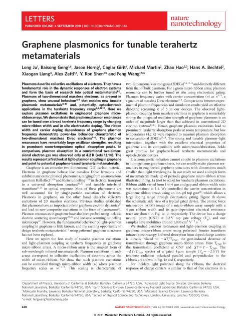
smaller than light wavelengths. In our study we used a simple <strong>for</strong>m<br />
of metamaterial made up of periodic graphene micro-ribbon arrays<br />
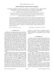
illustrated in Fig. 1a (not to scale) <strong>for</strong> <strong>terahertz</strong> plasmon excitations.<br />
Ribbon width varied from 1 to 4 mm and gap and ribbon width ratio<br />
was maintained at 1:1. We controlled the carrier concentration in<br />
graphene ribbon arrays using an ion-gel top gate 28 , which allows a<br />
large doping range through electrostatic gating. Figure 1b shows<br />
the schematic side view of a typical gated device. The atomic <strong>for</strong>ce<br />
microscopy (AFM) image of a micro-ribbon array sample with a<br />
4 mm ribbon width and its gate-dependent electrical resistance<br />
trace are shown in Fig. 1c, d, respectively. The device has a charge<br />
neutral point (CNP) at 0.2 V top gate voltage (V g), and our<br />
samples have mobilities around 1,000 cm 2 V 21 s 21 .<br />
We studied plasmon resonances and light–plasmon coupling in<br />
graphene micro-ribbon arrays using polarized Fourier trans<strong>for</strong>m<br />
infrared spectroscopy. Infrared absorption from doped charge carriers<br />
is directly related to 2DT/T CNP, the gate-induced decrease of<br />
transmission through graphene micro-ribbon arrays. Here T CNP is<br />
the transmission coefficient at CNP and DT ¼ T 2 T CNP. The<br />
2DT/T CNP spectra of a gated 4 mm sample (V g ¼ 22.0 V) <strong>for</strong><br />
<strong>terahertz</strong> radiation polarized parallel and perpendicular to the<br />
ribbons are shown in Fig. 1e and f, respectively.<br />
For incident light polarized along the ribbons, the electrical<br />
response of charge carriers is similar to that of free electrons in a<br />
1 Department of <strong>Physics</strong>, University of Cali<strong>for</strong>nia at Berkeley, Berkeley, Cali<strong>for</strong>nia 94720, USA, 2 Advanced Light Source Division, Lawrence Berkeley<br />
National Laboratory, Berkeley, Cali<strong>for</strong>nia 94720, USA, 3 Earth Sciences Division, Lawrence Berkeley National Laboratory, Berkeley, Cali<strong>for</strong>nia 94720, USA,<br />
4 Molecular Foundry, Lawrence Berkeley National Laboratory, Berkeley, Cali<strong>for</strong>nia 94720, USA, 5 Materials Science Division, Lawrence Berkeley<br />
National Laboratory, Berkeley, Cali<strong>for</strong>nia 94720, USA, 6 School of Physical Science and Technology, Lanzhou University, Lanzhou 730000, China.<br />
*e-mail: fengwang76@berkeley.edu<br />
630<br />
NATURE NANOTECHNOLOGY | VOL 6 | OCTOBER 2011 | www.nature.com/naturenanotechnology<br />
© 2011 Macmillan Publishers Limited. All rights reserved.
NATURE NANOTECHNOLOGY DOI: 10.1038/NNANO.2011.146 LETTERS<br />
homogeneous graphene sheet, and the spectral shape is well described<br />
by the Drude model as Im(21/(v þ iGD)) (black dashed line in<br />
Fig. 1e) with a scattering rate GD of 4 THz. This Drude absorption<br />
decreases monotonically with frequency v. For incident light<br />
polarized perpendicular to the ribbon, the resulting spectrum is<br />
completely different: an absorption peak originating from plasmon<br />
oscillation dominates the optical response (Fig. 1f). This plasmon<br />
absorption lineshape can be described by a damped oscillator as<br />
Im(2v /(v 2 2 v p<br />
a b c<br />
G<br />
30 nm d 25<br />
D<br />
Ion gel<br />
20<br />
D S<br />
15<br />
SiO2 10<br />
Si<br />
<strong>Graphene</strong><br />
8 μm<br />
5<br />
S SiO2 0 nm 0<br />
e 18<br />
−ΔT/T CNP (%)<br />
15<br />
12<br />
9<br />
6<br />
3<br />
0<br />
Expt<br />
Fitting<br />
ω (cm−1 100 200<br />
)<br />
300 400<br />
2 þ ivGp)) (blue dashed line) with a plasmon reson-<br />
ance v p of 3 THz and a spectral width G p of 4 THz. There is also a small<br />
background contribution from the free carrier absorption (magenta<br />
dashed line) because part of the infrared beam transmits through<br />
unpatterned graphene around the micro-ribbon array. The light–<br />
plasmon coupling in graphene is remarkably strong, with over 13%<br />
absorption at the plasmon resonance <strong>for</strong> one doped carbon monolayer.<br />
The observed plasmon resonance linewidth is similar to the Drude<br />
scattering rate <strong>for</strong> parallel light polarization, suggesting that plasmon<br />
broadening is largely limited by the same scattering processes affecting<br />
electrical transport.<br />
The light–plasmon coupling in graphene is remarkably strong<br />
compared with that in conventional 2DEGs in semiconductors, and<br />
arises from both the small effective electron mass and the efficient<br />
electrical gating in graphene. In conventional 2DEGs, the fieldinduced<br />
carrier concentration is limited to ≏1 × 10 12 cm 22 to avoid<br />
semiconductor dielectric breakdown. At this carrier density, the<br />
effective mass of an electron at Fermi energy is 0.02 m 0 in graphene.<br />
This electron effective mass is 3.5 (13) times smaller than that in<br />
GaAs (Si), and the integrated plasmon oscillator strength is correspondingly<br />
larger. In addition, graphene can be gated much more<br />
efficiently to over 1 × 10 13 cm 22 because of its excellent chemical<br />
stability and compatibility with different gating configurations.<br />
f<br />
−ΔT/T CNP (%)<br />
15<br />
12<br />
9<br />
6<br />
3<br />
0<br />
R (kΩ)<br />
−2 −1 0 1<br />
Vg (V)<br />
Expt<br />
Total<br />
Drude<br />
Plasmon<br />
ω (cm−1 100 200<br />
)<br />
300 400<br />
Figure 1 | Plasmon resonance in gated graphene micro-ribbon arrays. a, Top-view illustration of a typical graphene micro-ribbon array. The array was<br />
fabricated on transferred large-area CVD graphene using optical lithography and plasma etching. b, Side view of a typical device incorporating the graphene<br />
micro-ribbon array on a Si/SiO 2 substrate. The carrier concentration in graphene is controlled using the ion-gel top gate. c, AFM image of a graphene<br />
micro-ribbon array sample with a ribbon width of 4 mm and a ribbon and gap width ratio of 1:1. d, Gate-dependent electrical resistance of this graphene<br />
micro-ribbon array. The resistance has a maximum at charge neutral point V CNP ¼ 0.2 V. e,f, Gate-induced change of transmission spectra, 2(T 2 T CNP)/T CNP<br />
(red solid line), with incident light polarized parallel (e) and perpendicular (f) to the ribbon length, respectively. The gate voltage was set at V g ¼ 22V.For<br />
parallel polarization in e, the response originates from free carrier oscillation and can be well reproduced by a Drude fit (black dashed line). For perpendicular<br />
polarization in f, the spectrum shows a prominent absorption peak at 3 THz (1 THz ¼ 33.3 cm 21 ) because of plasmon excitation. Plasmon resonance is<br />
characterized by a Lorentzian lineshape (blue dashed line). A small free carrier contribution described by Drude absorption (magenta dashed line) isalso<br />
present as a result of graphene absorption outside the fabricated micro-ribbon array area. The plasmon absorption of over 13% is remarkably strong, and its<br />
integrated oscillator strength is more than an order of magnitude larger than that achieved in 2DEGs in conventional semiconductors.<br />
The resulting light–plasmon coupling in graphene can be an order<br />
of magnitude stronger than that achieved in conventional 2DEGs,<br />
and enabled us to observe <strong>terahertz</strong> plasmon resonance <strong>for</strong> the first<br />
time at room temperature.<br />
The plasmon resonance in graphene micro-ribbon arrays can<br />
be tuned in situ by electrostatic doping. For simplicity, we will<br />
focus on the hole-doping regime. We determine the gate-induced<br />
Fermi energy shift and carrier concentration in graphene through<br />
interband optical transitions 21,22 . This is based on the effect that<br />
interband transitions can be blocked up to 2|E F| energy in holedoped<br />
graphene as a result of empty initial states. Figure 2a shows<br />
gate-induced changes of interband transmission spectra in the<br />
3,000–9,000 cm 21 spectral range at different gate biases. Increased<br />
infrared transmission is observed up to a threshold energy that<br />
shifts to higher values with increased doping. This threshold<br />
energy is at 2|E F| (refs 21,22), from which carrier concentration<br />
can be deduced by n ¼ (|E F|/hv F) 2 /p (refs 15,16). Plasmon excitations<br />
in the graphene micro-ribbon array can be varied by<br />
electrical gating, as shown in Fig. 2b <strong>for</strong> absorption of perpendicularly<br />
polarized light. Prominent plasmon absorption peaks are<br />
observed, which shift to higher energies and gain oscillator strength<br />
with increased carrier concentration. For comparison, we show<br />
(in the inset of Fig. 2b) free carrier absorption spectra at different<br />
gate voltages (probed with light polarized parallel to microribbons).<br />
The spectral shape remains the same in all spectra,<br />
although the oscillator strength increases with carrier concentration.<br />
Plasmon excitations in graphene micro-ribbon arrays can also be<br />
controlled by engineering the ribbon width. Figure 2c shows AFM<br />
images of three micro-ribbon arrays with 1, 2 and 4 mm ribbon<br />
widths, respectively, and Fig. 2d shows 2DT/T CNP spectra <strong>for</strong> the<br />
three structures. All spectra were taken at the same hole-doping<br />
NATURE NANOTECHNOLOGY | VOL 6 | OCTOBER 2011 | www.nature.com/naturenanotechnology 631<br />
© 2011 Macmillan Publishers Limited. All rights reserved.
LETTERS<br />
a 101.0<br />
−2.2 V<br />
−1.8 V<br />
b<br />
100.8<br />
100.6<br />
−1.4 V<br />
−1.0 V<br />
−0.5 V<br />
T/T CNP (%)<br />
100.4<br />
100.2<br />
100.0<br />
99.8<br />
0<br />
4,000 6,000<br />
ω (cm<br />
8,000 100<br />
−1 )<br />
c d<br />
30 nm<br />
4 μm<br />
4 μm<br />
4 μm<br />
0 nm<br />
concentration of 1.5 × 10 13 cm 22 and were normalized by the<br />
respective peak values <strong>for</strong> convenience of comparison. The plasmon<br />
resonance clearly shifts to higher energy with decreasing ribbon<br />
widths: resonance frequencies are at 3, 4.1 and 6 THz <strong>for</strong> ribbon<br />
arrays of 4, 2 and 1 mm ribbon widths, respectively. Using nanoand<br />
micro-ribbon arrays with a larger range of ribbon widths, <strong>terahertz</strong><br />
resonance from 1–10 THz can be straight<strong>for</strong>wardly engineered.<br />
Next we examine the quantitative scaling behaviour of plasmon<br />
resonance frequency with carrier concentration and ribbon width.<br />
Figure 3a plots plasmon resonance frequencies as a function of |E F|<br />
(or equivalently |n| 1/2 in the top label) <strong>for</strong> different micro-ribbon<br />
widths. For a given carrier concentration, the plasmon resonance<br />
frequencies in different graphene micro-ribbon arrays are described<br />
by a scaling behaviour of v p / w 21/2 . This is best shown in Fig. 3b,<br />
where all data in Fig. 3a fit into a universal curve once the plasmon<br />
resonance frequencies are rescaled by w 21/2 .Thisscalingofv p with<br />
the inverse square root of the relevant spatial dimension is characteristic<br />
of 2DEGs 5,6 , in contrast to a constant plasmon resonance<br />
frequency in bulk plasmons. The universal relation between v p and<br />
|E F| in Fig. 3a can also be described by a power-law scaling with v p /<br />
|E F| 1/2 / n 1/4 (solid line). This power-law dependence of n 1/4 is a signature<br />
of massless Dirac electrons 4–6 , which is in contrast to n 1/2 scaling<br />
(dashed line) in conventional semiconductors.<br />
A theoretical understanding of the scaling behaviour of plasmon<br />
resonance in micro-ribbon arrays can be achieved using the quasistatic<br />
description, which is a good approximation <strong>for</strong> ribbon widths<br />
−ΔT/T CNP (%)<br />
−ΔT<br />
15<br />
10<br />
5<br />
1.0<br />
0.8<br />
0.6<br />
0.4<br />
0.2<br />
0.0<br />
15<br />
10<br />
(≏1 mm) much smaller than photon wavelengths (≏100 mm). The<br />
Maxwell equations satisfying the 2D ribbon array boundary conditions<br />
can be simplified to<br />
∂F<br />
∂y =−2pi<br />
∂<br />
kv ∂x s2DF(x) ∂F<br />
� �<br />
(1)<br />
∂x<br />
where k is the effective dielectric screening constant, s 2D is the 2D<br />
high-frequency conductivity at carrier concentration n, andF(x) is<br />
a square function with F(x) ¼ 1 at ribbon positions and F(x) ¼ 0<br />
in the gap (see Supplementary In<strong>for</strong>mation). By introducing<br />
dimensionless parameters X ¼ x/w and Y ¼ y/w and using the<br />
expression of s 2D <strong>for</strong> massless Dirac electrons, the above equation<br />
can also be expressed as<br />
with the dimensionless parameter<br />
5<br />
200<br />
−2.2 V<br />
−1.8 V<br />
−1.0 V<br />
200<br />
ω (cm<br />
300 400<br />
−1 )<br />
4 μm<br />
2 μm<br />
1 μm<br />
100 200 300 400<br />
ω (cm −1 )<br />
Figure 2 | Control of plasmon resonance through electrical gating and micro-ribbon width. a, Mid-infrared transmission spectra, T/T CNP , of the graphene<br />
ribbon array in Fig. 1 as gate voltage V g 2 V CNP varies from 20.3 to 22.2 V. The voltages corresponding to the unlabelled lines, starting with the red line and<br />
alternating downwards, are: 22.0 V, 21.6 V, 21.2 V, 20.7 V and 20.3 V. On electrical gating, optical transmission is increased up to a threshold energy<br />
of 2|E F| as a result of blocked interband optical transitions. This threshold energy provides direct determination of Fermi energy E F and carrier concentration<br />
n ¼ (|E F|/hv F) 2 /p in gated graphene. b, Control of <strong>terahertz</strong> resonance of plasmon excitations through electrical gating. Terahertz radiation was polarized<br />
perpendicular to the graphene ribbons. The plasmon resonance shifts to higher energy and gains oscillator strength with increased carrier concentration. For<br />
comparison, the inset shows corresponding spectra due to free carrier absorption <strong>for</strong> <strong>terahertz</strong> radiation polarized parallel to the ribbons. For this polarization,<br />
absorption strength increases with carrier concentration, but spectral shape remains the same. c, AFM images of samples with micro-ribbon widths (w) of1,<br />
2and4mm. d, Change of transmission spectra with different graphene micro-ribbon widths <strong>for</strong> the same doping concentration of 1.5 × 10 13 cm 22 .The<br />
Drude background contributed by unpatterned graphene around the arrays (as in Fig. 1f) was subtracted, and all spectra were normalized by their respective<br />
peak values <strong>for</strong> convenience of comparison. Plasmon resonance frequency v p shifts from 3 to 6 THz when micro-ribbon width decreases from 4 to 1 mm.<br />
632<br />
NATURE NANOTECHNOLOGY DOI: 10.1038/NNANO.2011.146<br />
� �<br />
∂F ∂ ∂F<br />
= h F(X)<br />
∂Y ∂X ∂X<br />
h = 2p1/2 vFe v(v + iG)<br />
2<br />
n<br />
h−<br />
1/2<br />
kw<br />
The electrodynamic responses of a micro-ribbon array are uniquely<br />
determined by the dimensionless parameter h. Maximum absorption<br />
NATURE NANOTECHNOLOGY | VOL 6 | OCTOBER 2011 | www.nature.com/naturenanotechnology<br />
© 2011 Macmillan Publishers Limited. All rights reserved.<br />
(2)
NATURE NANOTECHNOLOGY DOI: 10.1038/NNANO.2011.146 LETTERS<br />
a b<br />
2.0<br />
1 THz<br />
c<br />
2.0<br />
3 THz<br />
d<br />
2.0<br />
5 THz<br />
12<br />
Expt<br />
Simulation 1.5<br />
1.5<br />
1.5<br />
1.0<br />
1.0<br />
1.0<br />
–ΔT/T (%)<br />
9<br />
6<br />
3<br />
0<br />
100<br />
a<br />
ω p (cm −1 )<br />
200<br />
160<br />
120<br />
80<br />
1,500<br />
4 µm<br />
2 µm<br />
1 µm<br />
0 4<br />
X (μm)<br />
8<br />
ω (cm−1 200 300 400 0 4 8<br />
) X (μm)<br />
of incident light takes place at a specific h value, which determines<br />
the plasmon resonance frequency v p <strong>for</strong> given values of w and n.<br />
When either ribbon width or carrier concentration changes,<br />
plasmon frequency will change accordingly following the scaling<br />
behaviour of v p / n 1/4 . w 21/2 (<strong>for</strong> weak damping rate G), as<br />
observed experimentally.<br />
Although the differential equation readily explains the scaling<br />
behaviour of plasmon resonance frequency, it cannot be solved<br />
analytically <strong>for</strong> a quantitative value of v p. Instead, we use numerical<br />
calculations based on finite element methods to simulate this<br />
system, which has only one unknown parameter, namely the dielectric<br />
constant k. Using a k value of 5, the simulation (dashed line in<br />
Fig. 4a) reproduces well the observed 2DT/T CNP spectrum <strong>for</strong> a<br />
ribbon width of 4 mm and a doping concentration of 1.5 ×<br />
10 13 cm 22 (solid line in Fig. 4a). The k value of 5 is reasonable in<br />
our devices, given that the <strong>terahertz</strong> dielectric constants of ion gel,<br />
|n| b<br />
2.0 2.5 3.0 3.5<br />
0.0 1.0 2.0 3.0<br />
1/2 (106 cm−1 ) |n| 1/2 (106 cm−1 )<br />
|EF | (cm−1 )<br />
|EF | (cm−1 0<br />
2,000 2,500 3,000 3,500 4,000 0 1,000 2,000 3,000 4,000<br />
)<br />
Figure 3 | Scaling laws of graphene plasmon resonance frequency. a, Plasmon resonance frequency v p as a function of |E F| (or equivalently |n| 1/2 in the top<br />
label) <strong>for</strong> micro-ribbon arrays of different widths. b, Plasmon excitation v p was normalized by 1/ p w <strong>for</strong> micro-ribbon arrays of different widths, which fits all<br />
data points (symbols) into a universal curve (solid line). This w 21/2 scaling of v p is characteristic of 2D electron systems. The universal doping dependence<br />
of plasmon resonances is described by a scaling law of v p / |E F| 1/2 / n 1/4 .Thisn 1/4 scaling law is a signature of massless Dirac fermions. In comparison, v p<br />
scales as n 1/2 (dashed line) in conventional semiconductors.<br />
Amplitude (10 4 A m −1 )<br />
Phase (deg)<br />
0.5<br />
0<br />
80<br />
40<br />
0<br />
−40<br />
Amplitude (10 4 A m −1 )<br />
Phase (deg)<br />
0.5<br />
0<br />
80<br />
40<br />
0<br />
−40<br />
0 4<br />
X (μm)<br />
8<br />
0 4<br />
X (μm)<br />
8<br />
0 4<br />
X (μm)<br />
8<br />
0 4<br />
X (μm)<br />
8<br />
Figure 4 | Simulation of plasmon excitations. a, Transmission change spectrum 2DT/T CNP simulated by finite element analysis (dashed line) <strong>for</strong> the sample<br />
in Fig. 1 at carrier concentration of 1.5 × 10 13 cm 22 . It reproduces well the experimentally observed spectrum (solid line) when the effective environment<br />
dielectric constant k was set as 5, and corresponds to an electron–electron interaction strength of e 2 /khv F ≈ 0.4. b–d, Simulation results <strong>for</strong> current density<br />
amplitude (upper panel) and phase (lower panel) of the device at frequencies below resonance (1 THz, b), at resonance (3 THz, c) and above resonance<br />
(5 THz, d). The charge carriers oscillate perpendicular to the graphene ribbons on <strong>terahertz</strong> irradiation. The oscillating current is highest at the plasmon<br />
resonance frequency. The relative phase of the oscillating current with reference to the incident electrical field also varies quickly and changes sign at the<br />
resonance frequency. Both are characteristics of a resonant excitation.<br />
6<br />
SiO 2 and silicon are 3 (ref. 29), 4 and 11 (ref. 30), respectively.<br />
Such a dielectric screening constant will lead to an electron–electron<br />
interaction strength of a G ¼ e 2 /khv F ≈ 0.4.<br />
Figure 4b–d plots simulation results <strong>for</strong> current density amplitudes<br />
(top panels) and phases (bottom panels) in the same micro-ribbon<br />
array <strong>for</strong> frequencies below resonance (1 THz), at resonance (3 THz)<br />
and above resonance (5 THz), respectively. The current distribution<br />
describes electrons oscillating back and <strong>for</strong>th across the width of<br />
graphene micro-ribbons on <strong>terahertz</strong> radiation. The oscillating<br />
current amplitude is largest at the plasmon resonance frequency.<br />
Simultaneously, the phase of the current oscillation relative to that of<br />
the incident electric field varies quickly and changes sign across the<br />
resonance frequency. Both behaviours are typical characteristics of<br />
resonance excitation.<br />
Our studies show that plasmon resonances in graphene can be<br />
controlled in structure-engineered graphene micro-ribbon arrays,<br />
NATURE NANOTECHNOLOGY | VOL 6 | OCTOBER 2011 | www.nature.com/naturenanotechnology 633<br />
ω p * w 1/2 (10 9 m 1/2 Hz)<br />
4<br />
2<br />
4 µm<br />
2 µm<br />
1 µm<br />
© 2011 Macmillan Publishers Limited. All rights reserved.<br />
Amplitude (10 4 A m −1 )<br />
Phase (deg)<br />
0.5<br />
0<br />
80<br />
40<br />
0<br />
−40
LETTERS<br />
which represent the simplest <strong>for</strong>m of graphene <strong>terahertz</strong> <strong>metamaterials</strong>.<br />
Plasmons couple to <strong>terahertz</strong> radiation strongly, absorbing over<br />
13% at the plasmon resonance <strong>for</strong> half a monolayer material at room<br />
temperature. Peak absorption at resonance can become even stronger<br />
with reduced plasmon linewidth, which is currently limited by<br />
the scattering rate as in Drude conductivity. We expect that in<br />
higher-quality graphene samples, the plasmon linewidth will be<br />
reduced in proportion to the increase in mobility. The strong and<br />
broadly <strong>tunable</strong> plasmon resonances observed here in graphene<br />
micro-ribbon arrays can be generalized <strong>for</strong> designing more<br />
sophisticated <strong>metamaterials</strong> based on graphene, and enable new<br />
ways of controlling <strong>terahertz</strong> and far-infrared radiation.<br />
Methods<br />
Large-area graphene was grown using chemical vapour deposition on copper and<br />
transferred the graphene sheet onto a Si/SiO 2 wafer following ref. 31. Au/Cr<br />
electrodes of 50 nm thickness were deposited onto the graphene sheet in vacuum<br />
using stencil masks. Micro-ribbon arrays were fabricated in a 2.5 × 2.5 mm 2 area at<br />
the centre of the graphene sheet using standard optical lithography followed by<br />
oxygen plasma etching.<br />
Infrared transmission measurements were per<strong>for</strong>med with a Fourier<br />
trans<strong>for</strong>m infrared spectrometer at the Advanced Light Source in Lawrence Berkeley<br />
National Laboratory. All measurements were per<strong>for</strong>med in 0.1 torr vacuum at<br />
room temperature.<br />
Received 27 April 2011; accepted 27 July 2011;<br />
published online 4 September 2011<br />
References<br />
1. Yen, T. J. et al. Terahertz magnetic response from artificial materials. Science<br />
303, 1494–1496 (2004).<br />
2. Pendry, J. B., Holden, A. J., Stewart, W. J. & Youngs, I. Extremely low frequency<br />
plasmons in metallic mesostructures. Phys. Rev. Lett. 76, 4773–4776 (1996).<br />
3. Chen, H. T. et al. Active <strong>terahertz</strong> metamaterial devices. Nature 444,<br />
597–600 (2006).<br />
4. Wunsch, B., Stauber, T., Sols, F. & Guinea, F. Dynamical polarization of<br />
graphene at finite doping. New J. Phys. 8, 318 (2006).<br />
5. Polini, M., MacDonald, A. H. & Vignale, G. Drude weight, plasmon dispersion,<br />
and pseudospin response in doped graphene sheets. Preprint at http://arXiv.org/<br />
abs/0901.4528 (2009).<br />
6. Hwang, E. H. & Das Sarma, S. Dielectric function, screening, and plasmons in<br />
two-dimensional graphene. Phys. Rev. B 75, 205418 (2007).<br />
7. Brey, L. & Fertig, H. A. Elementary electronic excitations in graphene<br />
nanoribbons. Phys. Rev. B 75, 125434 (2007).<br />
8. Ashkan Vakil & Engheta, N. One-atom-thick IR <strong>metamaterials</strong> and<br />
trans<strong>for</strong>mation optics using graphene. Preprint at http://arXiv.org/abs/<br />
1101.3585 (2011).<br />
9. Jablan, M., Buljan, H. & Soljacic, M. Plasmonics in graphene at infrared<br />
frequencies. Phys. Rev. B 80, 245435 (2009).<br />
10. Koppens, F. H. L., Chang, D. E. & Abajo, F. J. G. d. <strong>Graphene</strong> <strong>plasmonics</strong>: a<br />
plat<strong>for</strong>m <strong>for</strong> strong light-matter interaction. Preprint at http://arXiv.org/abs/<br />
1104.2068v1 (2011).<br />
11. Rana, F. <strong>Graphene</strong> <strong>terahertz</strong> plasmon oscillators. IEEE Trans Nanotechnol.<br />
7, 91–99 (2008).<br />
12. Ryzhii, M. & Ryzhii, V. Injection and population inversion in electrically<br />
induced p-n junction in graphene with split gates. Jpn. J. Appl. Phys. 2 46,<br />
L151–L153 (2007).<br />
13. Allen, S. J., Tsui, D. C. & Logan, R. A. Observation of 2-dimensional plasmon<br />
in silicon inversion layers. Phys. Rev. Lett. 38, 980–983 (1977).<br />
634<br />
NATURE NANOTECHNOLOGY DOI: 10.1038/NNANO.2011.146<br />
14. Batke, E., Heitmann, D. & Tu, C. W. Plasmon and magnetoplasmon excitation in<br />
two-dimensional electron space-charge layers on gaas. Phys. Rev. B 34,<br />
6951–6960 (1986).<br />
15. Novoselov, K. S. et al. Two-dimensional gas of massless Dirac fermions in<br />
graphene. Nature 438, 197–200 (2005).<br />
16. Zhang, Y. B., Tan, Y. W., Stormer, H. L. & Kim, P. Experimental observation of<br />
the quantum Hall effect and Berry’s phase in graphene. Nature 438,<br />
201–204 (2005).<br />
17. Katsnelson, M. I., Novoselov, K. S. & Geim, A. K. Chiral tunnelling and the Klein<br />
paradox in graphene. Nature Phys. 2, 620–625 (2006).<br />
18. Young, A. F. & Kim, P. Quantum interference and Klein tunnelling in graphene<br />
heterojunctions. Nature Phys. 5, 222–226 (2009).<br />
19. Mak, K. F. et al. Measurement of the optical conductivity of graphene. Phys. Rev.<br />
Lett. 101, 246803 (2008).<br />
20. Nair, R. R. et al. Fine structure constant defines visual transparency of graphene.<br />
Science 320, 1308–1308 (2008).<br />
21. Li, Z. Q. et al. Dirac charge dynamics in graphene by infrared spectroscopy.<br />
Nature Phys. 4, 532–535 (2008).<br />
22. Wang, F. et al. Gate-variable optical transitions in graphene. Science 320,<br />
206–209 (2008).<br />
23. Bostwick, A., Ohta, T., Seyller, T., Horn, K. & Rotenberg, E. Quasiparticle<br />
dynamics in graphene. Nature Phys. 3, 36–40 (2007).<br />
24. Bostwick, A. et al. Observation of plasmarons in quasi-freestanding doped<br />
graphene. Science 328, 999–1002 (2010).<br />
25. Liu, Y., Willis, R. F., Emtsev, K. V. & Seyller, T. Plasmon dispersion and damping<br />
in electrically isolated two-dimensional charge sheets. Phys. Rev. B 78,<br />
201403 (2008).<br />
26. Tegenkamp, C., Pfnur, H., Langer, T., Baringhaus, J. & WSchumacher, H.<br />
Plasmon electron-hole resonance in epitaxial graphene. J. Phys. Condens. Matter<br />
23, 012001 (2011).<br />
27. Brar, V. W. et al. Observation of carrier-density-dependent many-body effects in<br />
graphene via tunneling spectroscopy. Phys. Rev. Lett. 104, 036805 (2010).<br />
28. Cho, J. H. et al. Printable ion-gel gate dielectrics <strong>for</strong> low-voltage polymer<br />
thin-film transistors on plastic. Nature Mater. 7, 900–906 (2008).<br />
29. Yamamoto, K., Tani, M. & Hangyo, M. Terahertz time-domain spectroscopy of<br />
imidazolium ionic liquids. J. Phys. Chem. B 111, 4854–4859 (2007).<br />
30. Palik, E. D. Handbook of Optical Constants of Solids (Elsevier, 1998).<br />
31. Li, X. S. et al. Large-area synthesis of high-quality and uni<strong>for</strong>m graphene films<br />
on copper foils. Science 324, 1312–1314 (2009).<br />
Acknowledgements<br />
The authors thank R. Sagelman and B. Boudouris <strong>for</strong> providing the ion gel and X. Zhang <strong>for</strong><br />
helpful discussions. This work was supported by an Office of Naval Research MURI award<br />
(N00014-09-1066 to L.J., J.H., C.G., A.Z. and F.W.) and the Office of Basic Energy Sciences,<br />
US Department of Energy (contract nos DE-AC02-05CH11231 <strong>for</strong> the Materials Science<br />
Division to Y.R.S. and F.W. and DE-AC02-05CH11231 <strong>for</strong> the Advanced Light Source).<br />
F.W. also acknowledges support from a Lucile and William Packard fellowship and a<br />
Hellman family fellowship, and L.J. acknowledges the support of a Lam fellowship.<br />
Author contributions<br />
F.W. and L.J. conceived the experiment. L.J. carried out optical measurements, B.G., J.H.,<br />
X.L. and C.G. contributed to sample growth and fabrication, and L.J. and F.W. per<strong>for</strong>med<br />
theoretical analysis. All authors discussed the results and wrote the paper.<br />
Additional in<strong>for</strong>mation<br />
The authors declare no competing financial interests. Supplementary in<strong>for</strong>mation<br />
accompanies this paper at www.nature.com/naturenanotechnology. Reprints and<br />
permission in<strong>for</strong>mation is available online at http://www.nature.com/reprints. Correspondence<br />
and requests <strong>for</strong> materials should be addressed to F.W.<br />
NATURE NANOTECHNOLOGY | VOL 6 | OCTOBER 2011 | www.nature.com/naturenanotechnology<br />
© 2011 Macmillan Publishers Limited. All rights reserved.