The Signetics 2650 - The MESSUI Place
The Signetics 2650 - The MESSUI Place
The Signetics 2650 - The MESSUI Place

You also want an ePaper? Increase the reach of your titles
YUMPU automatically turns print PDFs into web optimized ePapers that Google loves.
GETTING INTO MICROPROCESSORS<br />
<strong>The</strong> <strong>Signetics</strong> <strong>2650</strong><br />
We continue our survey of microprocessor chips and systems with this<br />
article, which takes a more detailed look at the <strong>Signetics</strong> <strong>2650</strong> device<br />
and its currently available evaluation kits. Although a relatively recent<br />
entry into the market, the <strong>2650</strong> has a particularly powerful instruction<br />
set and very flexible interfacing requirements. It seems likely to become<br />
the preferred 8-bit device for general purpose microcomputers.<br />
<strong>The</strong> <strong>Signetics</strong> <strong>2650</strong> is an 8-bit microprocessor<br />
which is made using well<br />
proven N-channel MOS technology. It<br />
runs from a single +5V supply, which<br />
tends to simplify power supply requirements.<br />
All inputs and outputs are TTL<br />
compatible, and the chip requires only<br />
a single-phase clock signal input. As the<br />
chip operates in static mode, there is no<br />
minimum clock frequency.<br />
With the original <strong>2650</strong> chip, the maximum<br />
clock frequency was 1.25MHz, giving<br />
instruction cycle times of from 4.8 to<br />
9.6 microseconds. However, the currently<br />
available <strong>2650</strong>-1 chip is rated to<br />
operate up to 2MHz, reducing the<br />
instruction cycle times to the range 3.6<br />
— 7.2us.<br />
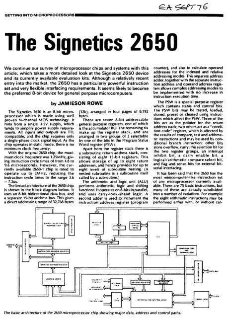
<strong>The</strong> broad architecture of the <strong>2650</strong> chip<br />
is shown in the block diagram below. It<br />
uses an 8-bit bidirectional data bus, and<br />
a separate 15-bit address bus. This gives<br />
a direct addressing range of 32,768 bytes<br />
50011511<br />
MA<br />
by JAMIESON ROWE<br />
T ■ J•N<br />
400•15.5 st ar.<br />
41.<br />
ssalinoL 'IOM £005415 RI GIST1 •<br />
051•540 4005151 5101511 0<br />
11<br />
500 5151 1D01•<br />
(32k), arranged in four pages of 8,192<br />
bytes.<br />
<strong>The</strong>re are seven 8-bit addressable<br />
general purpose registers, one of which<br />
is the accumulator RO. <strong>The</strong> remaining six<br />
make up the register stack, and are<br />
arranged in two groups of 3 selectable<br />
by one of the bits in the Program Status<br />
Word register (PSW).<br />
Apart from the register stack there is<br />
a subroutine return address stack, consisting<br />
of eight 15-bit registers. This<br />
allows storage of up to eight return<br />
addresses, and hence provides for up to<br />
eight levels of subroutine nesting. (A<br />
nested subroutine is a subroutine itself<br />
called by a subroutine.)<br />
<strong>The</strong> arithmetic and logic unit (ALU)<br />
performs arithmetic, logic and shifting<br />
functions. It operates on 8-bits in parallel,<br />
and uses carry-look-ahead logic. A<br />
second adder is used to increment the<br />
instruction address register (program<br />
atilt511,<br />
ST ar•<br />
INI 5 55.,55<br />
5.0•It TT<br />
INT( 55101<br />
/A VW/5n IIGT<br />
1,41504 LINIS<br />
5•TIRRI/51<br />
1'O<br />
LOGIC<br />
55045AM<br />
ST •T US<br />
.4050<br />
oNST RUCTION<br />
5(015115<br />
Of COOING £50 CONTROL LOCK<br />
<strong>The</strong> basic architecture of the <strong>2650</strong> microprocessor chip showing maior data, address and control paths.<br />
MOLT<br />
;(-,e-r7<br />
counter), and also to calculate operand<br />
addresses for the indexed and relative<br />
addressing modes. This separate address<br />
adder, together with the separate instruction<br />
address and operand address registers<br />
allows complex addressing modes to<br />
be implemented with no increase in<br />
instruction execution time.<br />
<strong>The</strong> PSW is a special purpose register<br />
which contains status and control bits.<br />
<strong>The</strong> PSW bits may be tested, loaded,<br />
stored, preset or cleared using instructions<br />
which affect the PSW. Three of the<br />
bits act as the pointer for the return<br />
address stack; two others act as a "condition<br />
code" register, which is affected by<br />
the results of compare, test and arithmetic<br />
instructions and may be used by conditional<br />
branch instruction; other bits<br />
store overflow, carry, the selection bit for<br />
the two register groups, an interrupt<br />
inhibit bit, a carry enable bit, a<br />
logical/arithmetic compare select bit,<br />
and flag and sense bits for external bitserial<br />
interfacing.<br />
It has been said that the <strong>2650</strong> has the<br />
most minicomputer-like instruction set<br />
of any microprocessor currently available.<br />
<strong>The</strong>re are 75 basic instructions, but<br />
many of these are actually subdivided<br />
into a number of variations. For example<br />
the eight arithmetic instructions may be<br />
performed either with, or without car-<br />
COTIOITIOM COO!<br />
550<br />
SITIOK5 LOOK<br />
THONG LOGIC<br />
DATA RUT<br />
CLOCK
GETTING INTO MICROPROCESSORS<br />
ry/borrow; this also applies to the two<br />
rotate instructions. Similarly the four<br />
compare instructions may perform either<br />
arithmetic or logical comparison, while<br />
four of the 12 branch instructions and six<br />
of the ten subroutine branch/return<br />
instructions are conditional upon the two<br />
PSW condition code bits—giving typically<br />
about 3 possible variants.<br />
Also although there are nominally only<br />
six input-output transfer (IOT) instructions,<br />
as distinct from the memory<br />
reference instructions (which may also<br />
be used for 10T), two of these are<br />
"extended" instructions which may<br />
address any one of 256 distinct 8-bit<br />
input-output ports.<br />
One, two and three-byte instructions<br />
are used, giving a high degree of<br />
programming efficiency. Register-toregister<br />
and simple IOT instructions are<br />
one byte, extended IOT instructions are<br />
two bytes, while memory-reference<br />
instructions are either two or three bytes<br />
long as required.<br />
<strong>The</strong> memory reference addressing<br />
modes provided by the <strong>2650</strong> are<br />
generally agreed to be the most extensive<br />
and versatile of any micro-processor<br />
currently available. <strong>The</strong> modes are as<br />
follows:<br />
1. Immediate addressing, with the data<br />
mask or value in the second byte of the<br />
instruction itself.<br />
2. Direct addressing, either absolute or<br />
program relative with a displacement<br />
range of from —64 to +63.<br />
3. Direct indexed addressing, absolute.<br />
4. Direct indexed addressing with auto<br />
increment.<br />
5. Direct indexed addressing with auto<br />
decrement.<br />
6. Indirect addressing, either absolute or<br />
n•<br />
CONTROL<br />
LINE<br />
SUFFERS<br />
MEM<br />
SELECT<br />
DECODE<br />
ADDRESS<br />
BUFF ER<br />
DATA<br />
SUFFER<br />
CONTROL<br />
DECODE<br />
PROM<br />
432X$)<br />
SERIAL<br />
1/0<br />
DRIVER/<br />
RECEIVER<br />
4-4<br />
SE L<br />
NON.<br />
EXTENDED<br />
INPUT<br />
II. XI<br />
PROM<br />
•OPREO. ntowirNIT. INTACK. was. Itws. witS. MA. FAME. WM. RESET,<br />
program relative with a displacement<br />
range of from —64 to +63.<br />
7. Indirect addressing with post indexing.<br />
8. Indirect addressing with post indexing<br />
and auto increment.<br />
9. Indirect addressing with post indexing<br />
and auto decrement.<br />
Memory and IOT interfacing of the<br />
<strong>2650</strong> is asynchronous, using "handshaking"<br />
control signals. This makes the <strong>2650</strong><br />
compatible with almost any type of<br />
SE L<br />
X S<br />
R AM<br />
I 'S 4<br />
ABUSE ABUSI.<br />
MUSE - DBUS7<br />
NON NON,<br />
EXTENDED EXTENDED<br />
OUTPUT INPUT<br />
2<br />
IS<br />
NON<br />
EXTENDED<br />
OUTPUT<br />
2<br />
<strong>The</strong> PC1001 evaluation board system, which is also pictured at top of this page.<br />
4<br />
I I ./<br />
TO BOARD EDGE CONNECTOR<br />
: ?4<br />
41. .44<br />
• •If 0<br />
memory and peripheral device.<br />
<strong>The</strong> <strong>2650</strong> has a single level vectored<br />
interrupt capability. Whei, it enters the<br />
interrupt mode, the chip is able to input<br />
an 8-bit address vector via the data bus.<br />
This may be used with either direct or<br />
indirect addressing to access interrupt<br />
servicing routines in any part of the<br />
memory space.<br />
As you should be able to see from this<br />
brief rundown of its salient features, the<br />
<strong>2650</strong> is a particularly flexible microprocessor,<br />
and one which is very well<br />
suited for general-purpose microcomputer<br />
applications. M such it would<br />
seem a good choice for anyone seeking<br />
to build up a minicomputer-type system<br />
based on a microprocessor.<br />
At the same time, the relatively low<br />
cost of the basic chip (currently around<br />
$20) and its ability to operate with little<br />
more than a clock generator and a ROM<br />
in dedicated mode would also make it<br />
a good choice for low level applications.<br />
<strong>Signetics</strong> make two evaluation kits<br />
based on the <strong>2650</strong>, and these are currently<br />
available in Australia from Philips.<br />
<strong>The</strong> more elaborate of the two is the<br />
PC1001, which comes as a ready-wired<br />
PC board together with edge connector<br />
socket and literature. <strong>The</strong> other kit is a<br />
little less elaborate, and comes as either<br />
a completely wired PC board or as an<br />
assemble-it-yourself kit. In wired form it<br />
is designated the PC1500, while the D-I-Y<br />
version is the KT9500.<br />
Both kits are basically small microcomputers,<br />
capable of being used directly<br />
with a power supply and an ASCII
GETTING INTO MICROPROCESSORS<br />
teleprinter to develop small <strong>2650</strong><br />
programs in machine language. <strong>The</strong>y<br />
could also be expanded into quite pretentious<br />
minicomputer systems, by<br />
adding further memory and IOT facilities.<br />
An add-on RAM memory board is in<br />
fact available, and is directly compatible<br />
with either kit. Designated the PC2000,<br />
it provides an additional 4k bytes of<br />
memory.<br />
At the time of writing this article, we<br />
have only had the opportunity to<br />
examine and use one of the PC1001<br />
evaluation kits. This is on a PC board<br />
measuring 203 x 175mm, with a 100-way<br />
double sided edge connector along one<br />
of the longer sides. <strong>The</strong> PC board is<br />
pictured, and as you can see there are<br />
quite a few IC's apart from the microprocessor.<br />
In fact the PC board is a three-layer<br />
assembly, with copper conductors sandwiched<br />
in between two layers of epoxyfibreglass<br />
as well as on the two external<br />
surfaces. This has allowed <strong>Signetics</strong> to fit<br />
a surprisingly large amount of circuitry on<br />
the relatively modest PCB area.<br />
On the PC1001 board is 1k bytes of<br />
RAM, capable of storing quite a respectable<br />
user program. In addition there is<br />
another 1k bytes of ROM, containing a<br />
resident monitor-debug program which<br />
<strong>Signetics</strong> have dubbed "PIPBUG". This<br />
will be described shortly.<br />
<strong>The</strong>re is an on-board serial asynchronous<br />
teleprinter interface, which<br />
may be adjusted by means of wire links<br />
for either 20mA current loop interfacing<br />
or RS232-type voltage interface.<br />
In addition to the teleprinter interface<br />
there are four 8-bit parallel IOT ports—<br />
two inputs and two outputs. <strong>The</strong>se are<br />
wired to be accessed via the two-byte<br />
"non-extended" IOT instructions, so that<br />
small systems with four or less<br />
peripherals (apart from the teleprinter)<br />
may be implemented with no further<br />
hardware.<br />
<strong>The</strong> PC1001 board has a 1MHz crystal<br />
clock, and therefore is immediately compatible<br />
with a 110-baud teleprinter (serial<br />
formatting is done by firmware routines,<br />
so baud timing is derived from the system<br />
clock).<br />
Full data and address bus buffering is<br />
provided on the PC1001 board, to simplify<br />
addition of further memory or<br />
peripherals. All of the control signals are<br />
also available at the edge connector in<br />
buffered form, which again simplifies any<br />
required interfacing.<br />
Although at the time of writing we<br />
have not had the opportunity to examine<br />
and use the PC1500/KT9500 evaluation<br />
kit, we understand that this is based on<br />
a PC board identical in size to that of the<br />
PC1001, And although the second kit is<br />
nominally a less pretentious one, it still<br />
offers quite impressive facilities.<br />
For example it still provides 1k bytes<br />
1111•111111111116. AIR
GETTING INTO MICROPROCESSORS<br />
of ROM, with the same resident monitordebug<br />
program (PIPBUG) provided on<br />
the PC1001. <strong>The</strong> only difference in terms<br />
of on-board memory is the RAM, which<br />
in this case is of only 512 bytes. This is<br />
still adequate for a lot of modest<br />
programming, of course—and you can<br />
always add further memory, as the board<br />
again provides fully buffered data,<br />
address and control signal buses.<br />
<strong>The</strong> serial asynchronous teleprinter<br />
interface is still provided, but there are<br />
now only two 8-bit parallel IOT ports.<br />
However, these are programmable in<br />
terms of direction, so that they may be<br />
used for both input and output.<br />
In place of the crystal clock, the<br />
PC1500/KT9500 has an R-C clock oscillator<br />
using a 74123 dual monostable.<br />
As not all of the PC board is used by<br />
the basic circuitry of the PC1500/KT9500<br />
system, the unused area is provided with<br />
plated through holes on 0.3in centres, to<br />
allow fitting of additional memory/<br />
peripheral decoding ICs if desired.<br />
In short, the PC1500/KT9500 evaluation<br />
kit is only a little less flexible than<br />
the PC1001. Both are in reality small<br />
development systems, capable of being<br />
used to develop and run <strong>2650</strong> programs.<br />
And in their basic form, each could be<br />
used to develop programs for running on<br />
the other—apart from the memory size<br />
difference. In that sense they are software<br />
compatible.<br />
Not only this, of course, but because<br />
they use the same resident monitordebug<br />
program they are also virtually<br />
identical in the operating sense.<br />
As evaluation kit resident debug<br />
programs go, PIPBUG seems quite a flexible<br />
one. It recognises seven basic commands,<br />
each of which consists of an<br />
alphabetic character, any required<br />
numerical parameters, and a terminating<br />
carriage return. <strong>The</strong> parameters are given<br />
as hexadecimal characters, with leading<br />
zeroes unnecessary.<br />
<strong>The</strong> seven commands and their functions<br />
are as follows:<br />
A — See and alter memory<br />
B — Set breakpoint (2 permitted)<br />
C — Clear breakpoint<br />
D — Dump memory to paper tape<br />
G — Go to address, run<br />
L — Load memory from paper tape<br />
S — See and alter registers<br />
<strong>The</strong> D command may be used to<br />
punch out any desired range of memory<br />
locations, with leader, checksum and<br />
trailer to facilitate reloading. Both the A<br />
and S commands may be auto-incremented,<br />
by terminating with a line feed<br />
instead of a carriage return.<br />
A full listing of PIPBUG is provided<br />
with the evaluation kits, which is very<br />
useful. Among other things, it allows the<br />
user to make use of the teleprinter servicing<br />
subroutines in PIPBUG, by arranging<br />
111111111111111111.111‘.<br />
SIMPLE ANSWER-BACK PROGRAM FOR SIGNETICS PC1001 SYSTEM<br />
DEVELOPED BY 4.1.ROWE,"ELECTRONICS AUSTRALIA" MAGAZINE 11/7/76<br />
NOTE: PROGRAM STARTS AT LOCATION 500 (HEX)<br />
LISTING:<br />
500 7o CO PPSU 4d /SET UP TTY<br />
5d2 3F d2 66 BSTA,UN CHIN /FETCh CHAR FnuN TTY VIA PIPBUG RTN<br />
505 Cl STRL,RI isa4g.<br />
506 3F 02 84 bSTA,UN COUT /ECHJ VIA PIPOUG ROUTINE<br />
509 01 LUDL,R1 /RESTjAE IN no<br />
50A A4 dJ SUI:11,Hd "CR" /ROm CRAP. -CR<br />
50C 58 74 BRNR,R0 -12 /CR? IF NOT KEEP GOING<br />
50E 04 OA LOD1.110 "LF" /SUPPLY LF<br />
510 3F 02 84 BSTA,UN CUUT<br />
513 05 00 LODI..111 /SET Rlm0<br />
515 OD 25 26 LODA,RI 526+ /FETCH A(JSWER CHAR<br />
518 C3 STAZ,R3 /SAVE<br />
519 3F 02 B4 BSTA,UW COUT /PRINT<br />
51C A7 OD SUBI,R3 "CR" /R3m CHAR -CR<br />
51E 58 75 BRNR,R3 -11 /CR? IF NOT KEEP 601NG<br />
520 04 OA LODI,R0 "LF" /YES; SUPPLY LF<br />
522 3F 02 B4 BSTA,UN COUT<br />
525 18 5A BCTR,UN -36 /BACK Tu LuUK FOR NEW INPUT<br />
527 47 4F 20 /START OF ANSWER SUFFER<br />
52A 41 57 41<br />
52D 59 2C 49<br />
530 27 4D 20<br />
533 42 55 53<br />
536 59 21 OD /AWSWZR LUST END WITH CH (HEX OD)<br />
SAMPLE OF OPERATION:<br />
*u500<br />
HELLO THERE, WhAT AT PRESENT ARE YOU COMPUTING?<br />
GO AWAY,I'M BUSY!<br />
DON'T BE LIKE THAT,PLEASE<br />
GO AWAY,I'M SUSYI<br />
This simple novelty program was written largely to verify that the teletype servicing<br />
routines in PIPBUG could be called by a user program. <strong>The</strong> listing shows instruction<br />
mnemonics and comments as well as the actual instructions in hexadecimal code.<br />
for application programs to call them as<br />
required.<br />
To illustrate this, the author wrote a<br />
simple novelty program for the PC1001<br />
system. Its listing and a sample of the<br />
operation are reproduced on these<br />
pages, and as you can see it does nothing<br />
more than monitor input from the<br />
teleprinter, waiting for the person at the<br />
keyboard to press the carriage return<br />
key. When this occurs, it responds by<br />
typing out a curt reply: "GO AWAY, I'M<br />
BUSY!".<br />
I wrote this little program mainly for<br />
practice with the <strong>2650</strong> instruction set, and<br />
also to check out the use of the PIPBUG<br />
teleprinter servicing routines. <strong>The</strong> pro--<br />
gram inputs characters via the "CHIN"<br />
subroutine in PIPBUG, whose calling<br />
address is 0286, and outputs characters<br />
via the "COUT" subroutine whose calling<br />
address is 0284. As you can see the<br />
program itself starts at location 0500.<br />
Note that the program uses one, two<br />
and three-byte instructions, and requires<br />
only 57 bytes of memory including the<br />
answer message buffer. This illustrates<br />
the programming efficiency possible<br />
with the <strong>2650</strong>'s powerful instruction set<br />
and wealth of memory addressing<br />
modes.<br />
If you're interested in the PC1001 or<br />
the PC1500/KT9500 evalution kits or the<br />
PC2000 add-on memory, they are available<br />
from the Electronic Components<br />
and Materials Division of Philips Industries,<br />
with offices in each state, or from<br />
their distributors. Prices for the kits are<br />
as follows:<br />
PC1001 — $345 plus tax<br />
PC1500 — $245 plus tax<br />
KT9500 — $165 plus tax<br />
.PC2000 — $400 plus tax<br />
Each of the basic kits comes with all<br />
of the literature needed to use it. All you<br />
need is a power supply and a teleprinter.<br />
<strong>The</strong> teleprinter must communicate<br />
in ASCII code, as with most<br />
other kits. Here at EA we are currently<br />
working on a way to allow this to be<br />
done at low cost using a surplus Baudot<br />
teleprinter.
GETTING INTO MICROPROCESSORS<br />
A "baby" system using<br />
the <strong>Signetics</strong> <strong>2650</strong><br />
Here is surely the simplest and lowest-cost way of getting to know the<br />
<strong>Signetics</strong> <strong>2650</strong> microprocessor. A complete microcomputer system on<br />
a single small PC board, you can build it for around $70, not counting<br />
a power supply or terminal. Despite its low cost, it offers the same<br />
debug and monitor program in ROM provided by more expensive systems,<br />
together with 256 words of RAM.<br />
As we have noted in earlier articles, the<br />
<strong>Signetics</strong> <strong>2650</strong> microprocessor is a particularly<br />
powerful device. Its architecture<br />
and instruction set are very minicomputer-like,<br />
making it well suited for<br />
general-purpose computing as well as<br />
low-cost dedicated applications.<br />
In their literature, <strong>Signetics</strong> note that<br />
the device may be used to implement a<br />
very low cost minimal "evaluation kit"<br />
type system, one which would be very<br />
suitable for those wishing to gain<br />
experience with the <strong>2650</strong> with the<br />
minimum outlay of both time and<br />
money. However they themselves have<br />
not made such a minimal evaluation system<br />
available, only larger systems such<br />
as the PC1001 and PC1500 systems.<br />
This seemed rather a pity to us, as at<br />
least one other microprocessor has been<br />
available in a really minimal system, and<br />
this has proved very popular. However<br />
as the <strong>2650</strong> and its 2608 ROM chip have<br />
been in rather short supply until recently,<br />
there seemed little hope of being able to<br />
remedy the situation as far as the <strong>2650</strong><br />
was concerned.<br />
Happily this situation has now changed<br />
by JAMIESON ROWE<br />
68 ELECTRONICS Australia, March, 1977<br />
for the better. Just a few weeks ago we<br />
learned from Philips Industries that the<br />
<strong>2650</strong> and 2608 chips were now readily<br />
available, and at relatively low cost. (<strong>Signetics</strong><br />
is a US subsidiary of Philips.) We<br />
accordingly suggested to them that this<br />
would be an ideal opportunity to produce<br />
a low-cost "baby" <strong>2650</strong> system,<br />
based on the minimal system suggested<br />
by <strong>Signetics</strong> themselves. <strong>The</strong>y agreed,<br />
and offered to make available a set of<br />
devices if we cared to try the idea.<br />
This project is the result!<br />
Basically, it is a complete generalpurpose<br />
microcomputer, just like the larger<br />
evaluation kits. In fact it has the same<br />
debug and monitor program as the larger<br />
kits—"PIPBUG"—resident in the 2608<br />
ROM (1k x 8-bit words). It communicates<br />
directly with a standard 20mA<br />
asynchronous data terminal, such as an<br />
ASR-33 Teletype or the video data terminal<br />
described in our January and<br />
February issues, and requires a single 5V<br />
DC power supply.<br />
<strong>The</strong> main difference between this system<br />
and the larger systems is that there<br />
is only 256 bytes of RAM memory for<br />
user program storage, and there is no onboard<br />
decoding or buffering for further<br />
memory or peripheral expansion.<br />
In short, it is a "bare minimum" <strong>2650</strong><br />
system, designed to be the cheapest and<br />
easiest way of getting a <strong>2650</strong> up and running.<br />
At the same time, it offers the full<br />
program development facilities of<br />
PIPBUG, including the ability to examine<br />
and alter memory from the terminal<br />
keyboard; the ability to dump programs<br />
to paper tape or cassette, and then load<br />
memory from tape; the ability to<br />
examine and set the processor registers;<br />
the ability to set and remove up to two<br />
breakpoints, for debugging; and the<br />
ability to run the user's program on command.<br />
<strong>The</strong>se are quite powerful program<br />
development facilities, not usually found<br />
on low cost systems. As a result, our<br />
"baby" <strong>2650</strong> microcomputer should be<br />
particularly suitable for edutational and<br />
training purposes, whether by schools<br />
and colleges or by individual enthusiasts.<br />
As you can see from the diagrams and<br />
photograph, it consists of only a handful<br />
of parts on a small PC board. <strong>The</strong>re are<br />
only six ICs, one transistor and a few<br />
resistors and capacitors, and the PCB is<br />
single-sided to keep the cost down.<br />
Heart of the circuit is the <strong>2650</strong> chip<br />
itself, a powerful 8-bit microprocessor<br />
with an instruction set of 75 instructions,<br />
and eight different addressing modes.<br />
Fabricated using low-threshold ion<br />
implantation, it is an N-channel silicon<br />
At left is our new "baby" <strong>2650</strong><br />
microcomputer, complete on<br />
its small PC board. It offers the<br />
same PIPBUG program in<br />
ROM as provided on the larger<br />
systems. <strong>The</strong> full circuit<br />
diagram is shown on the facing<br />
page, together with an<br />
optional power supply.
C.<br />
CD 0<br />
C')<br />
N<br />
•71.<br />
0<br />
Cy)<br />
CO CO Co 0 r N<br />
NNNNintne.101<br />
N ‘1. M N r 0<br />
O 0000000<br />
0<br />
N<br />
N<br />
W<br />
co<br />
N2 /<br />
0 •<br />
r r < to Q<br />
• N 14<br />
CD 0<br />
• 0<br />
C.)<br />
0<br />
Co<br />
N<br />
O<br />
W<br />
co<br />
C)<br />
o.<br />
cc<br />
co<br />
• cvi<br />
•<br />
co<br />
cc<br />
Cn<br />
co<br />
co<br />
Co<br />
4<br />
C■1<br />
CO al<br />
Oa <<br />
CO<br />
N 0<br />
<<br />
Q<br />
cc In<br />
C.)<br />
N<br />
Cl)<br />
C)<br />
In<br />
cc<br />
co<br />
C.)<br />
O<br />
Cl)<br />
C)<br />
Co<br />
0<br />
CC<br />
N<br />
et en *- 0<br />
us co Co 1 MI C41 7,11.1.21 - 141N N<br />
O r N M tt to CO N CO Co 0 r- N<br />
O 0000001:100".,.7 W<br />
< < < < < < < 0 CC IC -<br />
<
GETTING INTO MICROPROCESSORS<br />
gate device which operates from a single<br />
5V supply and offers TTL compatibility<br />
on all inputs and outputs.<br />
A 74123 dual monostable device is<br />
used to generate the single-phase 1MHz<br />
clock signals fol. the <strong>2650</strong>. <strong>The</strong> clock<br />
oscillator is of the R-C type, but is easily<br />
adjusted to the correct operating<br />
frequency without the need for elaborate<br />
instruments. More about this later on .. .<br />
As mentioned already, the PIPBUG<br />
debug-monitor program is resident in a<br />
2608 ROM. This includesroulln- es for servicing<br />
the data terminal input and output,<br />
so that the system "knows" how to communicate<br />
with a terminal as soon as it is<br />
initialised. <strong>The</strong> code suffix for the 2608<br />
with PIPBUG resident is CN0035.<br />
Two 2112 devices are used to provide<br />
the. RAM memory of the system. <strong>The</strong>se<br />
are low-cost static MOS RAMs, each<br />
organised as 256 words or 4 bits, so that<br />
the two together provide a RAM of 256<br />
8-bit words. Some 63 words are used by<br />
PIPBUG as its scratchpad area, leaving<br />
193 available for user programs.<br />
<strong>The</strong> remaining IC in the circuit is a<br />
74LS38 low-power Schottky quad NAND<br />
buffer, two gates of which are used for<br />
simple address decoding to allow the<br />
<strong>2650</strong> to differentiate between the ROM<br />
and RAM sections of memory.<br />
<strong>The</strong> ROM is allocated to the address<br />
range 000-3FF hexadecimal, or the first<br />
1k of memory space. <strong>The</strong> RAM memory<br />
is allocated to the next 256 bytes of<br />
memory space, with hexadecimal<br />
addresses 400-4FF. Basically this means<br />
that when binary address bit AD10 is 0,<br />
the ROM is selected, while when it is 1<br />
the RAM memory is selected.<br />
Gate G3 is used to enable the two 2112<br />
RAM devices when AD10 is at the 1 level.<br />
<strong>The</strong> second input of G3 is fed with the<br />
OPREQ signal from the <strong>2650</strong>, which is a<br />
strobing signal used to indicate when bus<br />
information is valid.<br />
When AD10 is at the 0 level, the RAMs<br />
are therefore disabled. At the same time<br />
the ROM is enabled, because the AD10<br />
signal from the <strong>2650</strong> is also fed to the<br />
active-low chip-select input CS1 of the<br />
2608 ROM device. Correct strobing of<br />
the ROM is achieved by using gate G4<br />
as an inverter to feed an OPREQ-bar signal<br />
to the CSO input of the ROM.<br />
Note that this simple address decoding<br />
scheme is not completely unambiguous,<br />
because the ROM is enabled whenever<br />
AD10 is 0 and the RAMs whenever it is<br />
1. Thus the ROM strictly occupies not<br />
only the nominal range of 000-3FF, but<br />
also higher ranges such as 800-BFF.<br />
Similarly the RAMs occupy not only their<br />
nominal range 400-4FF, but also higher<br />
ranges such as 500-5FF, 600-6FF, 700-7FF,<br />
C00-CFF, D00-DFF, E00-EFF, and<br />
FOO-FFF.<br />
This ambiguity need not cause any<br />
complications, however, providing you<br />
Using this overlay diagram you should have no problems in fitting the components<br />
to the PC board. Sockets are used for the <strong>2650</strong> and 2608 devices.<br />
LIST OF PARTS<br />
1 PC board, 175 x 135mm, code<br />
77up2<br />
8 PCB terminal pins (optional)<br />
1 <strong>2650</strong> microprocessor IC<br />
1 2608 ROM (with PIPBUG: code<br />
CN0035)<br />
2 2112B RAMs<br />
1 74123 dual monostable<br />
1 74L538 low-power Schottky buffer<br />
1 BC548 or similar NPN silicon<br />
1 1N914, 1N1418 or similar diodes<br />
1 40-pin IC socket, PC type<br />
1 24-pin IC socket, PC type<br />
remember it and take it into account<br />
when writing your programs. All it means<br />
is that if you forget and your program<br />
tries to address these non-existent higher<br />
memory locations, it will in reality still be<br />
talking to the same ROM and RAMs!<br />
Many small systems use this type of<br />
simple address decoding, to simplify the<br />
circuitry and reduce costs.<br />
<strong>The</strong> third gate, G2, is used to control<br />
the read-write function selection of the<br />
RAM devices. <strong>The</strong> inputs of the gate are<br />
fed from the R-bar/W and WRP outputs<br />
of the <strong>2650</strong>, while its output goes to the<br />
R/W-bar control inputs of the 2112 RAM<br />
devices. <strong>The</strong> R-bar/W output of the <strong>2650</strong><br />
provides its read-write control signal,<br />
while the WRP output provides a write<br />
strobe pulse designed to delay writing<br />
until memory devices have stablised.<br />
<strong>The</strong> remaining section of the circuit is<br />
that used to provide the serial com-<br />
RESISTORS<br />
Quarter watt, 5%: 150ohms, 4 x 1k, 3<br />
x 1.5k, 2 x 2.2k, 1 x 3.3k, 2x 10k,<br />
1 x 22k.<br />
1 47k PC type tab pot, vertical<br />
mount<br />
CAPACITORS<br />
1 47pF NPO ceramic<br />
1 330pF NPO ceramic<br />
5 .047uF LV polyester<br />
1 0.22uF LV polyester<br />
1 1.5uF 35VW electro or tantalum<br />
Wire for links, solder, etc.<br />
munication ports, which are associated<br />
with the flag (F) output and sense (S)<br />
input of the <strong>2650</strong>. <strong>The</strong> output port uses<br />
the remaining gate G1 as a buffer, to control<br />
a 20mA output current in response<br />
to the F output of the microprocessor.<br />
<strong>The</strong> 150-ohm resistor in series with the<br />
gate output sets the output current level,<br />
which is sufficient to drive the normal<br />
current-loop input of an ASCII teleprinter<br />
or video data terminal.<br />
<strong>The</strong> input port circuitry uses a BC548<br />
or similar general-purpose NPN transistor<br />
T1 to provide level translation between<br />
a standard 20mA current loop<br />
input and the S input of the microprocessor.<br />
<strong>The</strong> input circuit provides its own<br />
20mA source, and so is suitable for direct<br />
connection to the keyboard contacts of<br />
a teleprinter, or the corresponding output<br />
terminals of a video data terminal<br />
such as that described last month.<br />
ELECTRONICS Australia, March, 1977 71
GETTING INTO MICROPROCESSORS<br />
<strong>The</strong> 1.5uF capacitor in the base circuit<br />
of T1 is to provide contact bounce<br />
suppression in the case of teleprinter<br />
keyboards, and also to provide filtering<br />
of any noise induced in the input line.<br />
<strong>The</strong> two diodes are to protect the transistor<br />
from high amplitude noise impulses.<br />
As you can see, the complete baby system<br />
is built up on a small PC board<br />
measuring 175 x 135mm. <strong>The</strong> pattern is<br />
coded 77up2, and PC boards etched to<br />
the pattern should be available from<br />
board manufacturers by the time you<br />
read this article.<br />
Assembly of the system on the PCB<br />
should be fairly straightforward using the<br />
overlay diagram as a guide. Note that<br />
there are a number of wire links, necessary<br />
because the board has been kept<br />
single-sided.<br />
In view of the fact that the <strong>2650</strong><br />
microprocessor chip and the 2608 ROM<br />
are both fairly expensive, and are both<br />
MOS devices, I suggest that you use<br />
sockets for them. A 40-pin socket is<br />
required for the <strong>2650</strong>, and a 24-pin socket<br />
for the 2608, both being of the 0.6in row-<br />
Below is the PCB pattern, actual size for<br />
those wishing to etch their own.<br />
72 ELECTRONICS Australia, March, 1977<br />
spacing DIL type. Use high quality<br />
sockets if you can, to avoid contact troubles.<br />
<strong>The</strong> remaining ICs are probably best<br />
soldered directly into the PC board.<br />
I suggest that you wire in all of the links<br />
first, then add the IC sockets and the<br />
resistors and capacitors. Watch the<br />
polarity of the 1.5uF tantalum electrolytic,<br />
as this could cause malfunction if it is<br />
connected the wrong way around.<br />
Now wire in the transistor, the two<br />
diodes and the two TTL ICs (74123 and<br />
74LS38), taking care that these are also<br />
orientated correctly. <strong>The</strong>n finally add the<br />
two RAMs, after having connected the<br />
barrel and bit of your soldering iron to<br />
the PCB supply lines to ensure that the<br />
MOS ICs won't be damaged by static<br />
charge. It is a good idea to solder the<br />
supply pins of each IC first (pins 7 and<br />
14), so that the internal protection diodes<br />
become operational as soon as possible.<br />
<strong>The</strong>re are only eight external connections<br />
to the PC board. Two are for the<br />
power supply, which may be almost any<br />
reasonably well regulated and filtered 5V<br />
DC supply. <strong>The</strong> total current drain is<br />
around 250mA. If you don't have a suit-<br />
able supply handy, the circuit shown in<br />
the small diagram would be quite suitable.<br />
<strong>The</strong> four connection points adjacent to<br />
one another are for the serial input and<br />
output. <strong>The</strong>se connect to the teleprinter<br />
or video data terminal, with polarities as<br />
shown. Whichever type of terminal is<br />
used, it should be connected for 20mA,<br />
full duplex operation.<br />
<strong>The</strong> remaining two connections to the<br />
PCB go to the reset switch, which is a<br />
simple normally-closed pushbutton.<br />
When pressed, this button forces the<br />
microprocessor to reset its internal registers.<br />
<strong>The</strong>n when the button is released<br />
the microprocessor begins running from<br />
a known and predetermined state, fetching<br />
its first instruction from memory location<br />
000—the start of the PIPBUG<br />
program residing in ROM.<br />
<strong>The</strong> reset button therefore serves to<br />
initialise the system, and is used for this<br />
purpose both when power is first<br />
applied, and at other occasions<br />
whenever one wishes to return to<br />
PIPBUG from an applications program<br />
(apart from breakpoint returns, which<br />
take place automatically).
GETTING INTO MICROPROCESSORS<br />
When you have completed wiring the<br />
PC board and connected it up to the terminal,<br />
reset switch and power supply,<br />
carefully remove the <strong>2650</strong> and 2608 chips<br />
from their conductive foam and plug<br />
them into their respective sockets (with<br />
the power turned off).<br />
<strong>The</strong>re is only one adjustment to be<br />
made, that in which the 74123 clock<br />
oscillator is set up to operate at the correct<br />
frequency of 1MHz. This is done<br />
with power applied.<br />
If you have access to a frequency counter,<br />
it can be done by simply connecting<br />
the counter between pin 5 of the 74123<br />
and the grounded negative supply rail,<br />
and adjusting the small tab pot until the<br />
counter reads 1MHz. This is the preferred<br />
way of setting the clock frequency.<br />
However if you don't have access to<br />
a counter, the frequency can still be set<br />
up fairly accurately using the teleprinter<br />
or data terminal itself. This can be done<br />
because only when the clock frequency<br />
is the correct 1MHz will the softwaretimed<br />
serial output signals produced by<br />
the <strong>2650</strong> be at the correct 110-baud data<br />
rate required by the terminal.<br />
To adjust the clock frequency using<br />
this method, apply power to both the<br />
system and the terminal. <strong>The</strong>n press the<br />
reset button, and release. <strong>The</strong> printer of<br />
the Teletype or the screen of the video<br />
terminal should print a couple of<br />
characters and then become static.<br />
If by some lucky chance you have the<br />
correct clock frequency already, the<br />
printer or display screen should have<br />
displayed a carriage return (CR), a line<br />
feed (LF), and an asterisk. This is the<br />
programmed output of the PIPBUG<br />
program upon initialisation (the asterisk<br />
is its prompt signal, signifying readyness<br />
for an input command).<br />
Most likely, you won't get this<br />
sequence of CR-LF-asterisk straight<br />
away. But the idea is to adjust the tab pot<br />
slowly and carefully from its maximum<br />
resistance extreme, pressing the reset<br />
switch after each change until you find<br />
the setting where the terminal shows that<br />
the characters are being fed to it at the<br />
correct rate.<br />
<strong>The</strong>re should be a small zone of the<br />
pot's travel in which the characters are<br />
printed correctly following the release of<br />
the reset button. For most reliable operation,<br />
try to set the pot in the middle of<br />
this zone.<br />
With this adjustment made, your baby<br />
<strong>2650</strong> system is fully operational and ready<br />
to begin work (or play!). With the set of<br />
ICs, you should have received a <strong>Signetics</strong><br />
Applications Memo (coded 5550) which<br />
explains how to use PIPBUG to feed<br />
applications programs into the system,<br />
run them, debug them, dump them on<br />
paper tape (or cassette), and re-load<br />
them. It also gives a listing of PIPBUG<br />
itself, which among other things lets you<br />
make use of some of its utility subrou-<br />
SIMPLE ANSWER-BAC PROGRAM FOR "BABY" <strong>2650</strong> MICROCOMPUTER<br />
',MITTEN BY J.ROTjE,' "ELECTRONICS AUSTRALIA" MAGAZINE<br />
ADD. CODE MNEMONICS co MU aJ TS<br />
440 76 CO PPSU 40 / SET T TY TO M ARN<br />
442 3F 02 06 3STA,UN CHIN /FETCH CHAP VIA PI ?BUG RTN<br />
445 C 1 STRZ, R1 / SAVE<br />
446 3F 02 34 ESTA, UN COUT /FCHO<br />
449 01 LODZ, R1 /RESTO RE IN R0<br />
44A A4 OD SUBI RO "CR" /TEST FOR CR<br />
44C 58 74 BRNR, RO - 12 /KEEP GOING IF NOT<br />
44E 04 0A LO DI , RO "LF" /IF YES,PROVIDE LF<br />
450 3F 02 34 BSTA, UN COUT<br />
453 05 00 LODI,R1 /SET R1=0<br />
455 OD 24 66 LO DA, R1 466+ /FETCH ANSWER CHAR<br />
458 C3 STRZ, R3 / SAVE<br />
459 3F 02 54 BSTA, UN COUT /PRINT<br />
45C A7 OD SIMI, R3 "CR" /TEST FOR CR<br />
45E 5B 75 BRNR, R3 - 11 /IF NO T, KEEP GOING<br />
460 04 0A LO DI, RO "LF" / I F YES, SUPPLY LF<br />
462 3F 02 D4 BSTA, UN COUT<br />
465 13 5A BCTR, UN - 38 /BACK TO START AGAIN<br />
467 47 4F 20 /ANSWER TEXT<br />
46A 41 57 41<br />
46D 59 2C 49<br />
470 27 4D 20<br />
473 42 55 53<br />
476 59 21 OD /ANSWER MUST END WITH A CR-<br />
This simple novelty program should help you get your system going. Only the code<br />
is actually fed into RAM, starting at location 440 hex.<br />
tines such as the serial input and output<br />
routines "CHIN" and "COUT".<br />
To help you get your system up and<br />
running, a listing is shown for a modified<br />
version of the novelty answer-back<br />
program which the author originally<br />
wrote for the larger PC1001 system. Note<br />
that all you actually enter into the system<br />
are the two-digit hexadecimal machine<br />
code words; the mnemonics and cornments<br />
are purely to help follow how the<br />
program works.<br />
To feed the program into the system,<br />
you use the PIPBUG "A" command,<br />
typing first "A 440" and then a carriage<br />
return. PIPBUG will then type out on the<br />
next line "440 XX", where XX is the current<br />
content of location 440 (probably<br />
random). It then pauses. You then type<br />
"76", followed by a line feed, whereupon<br />
PIPBUG does a CR-LF, and then prints<br />
For those with a bigger<br />
system in mind:<br />
If your ultimate aim is to build up a large<br />
<strong>2650</strong> system, it may be better for you to<br />
start with the single-board system shown<br />
at right, than with our "baby". Available<br />
both as an assembled system (code<br />
PC1500) and as a do-it-yourself kit<br />
(KT9500), it provides all of the features<br />
of the baby system together with full<br />
memory decoding, fully buffered data<br />
and address lines, and two bidirectional<br />
8-bit input/output ports. Further details<br />
are available from Philips distributors.<br />
out the next memory address and its current<br />
content. You then type "CO" and LF,<br />
and so on until all of the program has<br />
been fed in.<br />
<strong>The</strong>n to run the program, type "G 440"<br />
followed by a CR. PIPBUG will then<br />
transfer you to the program in RAM.<br />
Try typing in a comment, ending it with<br />
a carriage return. <strong>The</strong> program should<br />
answer with a terse "GO AWAY, I'M<br />
BUSY!"<br />
When you get tired of this reply, it can<br />
be changed by feeding in a new string<br />
of ASCII characters starting at address<br />
467 hex. Note, however that the message<br />
must end with a CRR (hex OD).<br />
Of course this is just a demonstration<br />
program, to get you going. <strong>The</strong> next step<br />
is to write your own, using as a guide the<br />
<strong>Signetics</strong> <strong>2650</strong> programming book supplied<br />
with the kit. Happy computing!<br />
ELECTRONICS Australia, March, 1977 73
START WITH THE INCREDIBLY SIMPLE<br />
<strong>2650</strong>-KT95EA<br />
"BABY MICROPROCESSOR KIT"<br />
NEW SOUTH WALES:Applied<br />
Technology,CEMA, Electronic<br />
Enthusiasts, ICS, Tecnico (Sydney),<br />
Digitronics (Newcastle),<br />
Macelec (Wollongong)<br />
ACT: Daicom<br />
QUEENSLAND: Electronic<br />
Components, Fred Hoe,<br />
NS Electronics<br />
ELECTRONICS Australia, April, 1977<br />
NOW AVAILABLE FROM THESE<br />
PHILIPS SIGNETICS STOCKISTS<br />
VICTORIA: CEMA, ICS, Sontron,<br />
Sycom, Tecnico<br />
SOUTH AUSTRALIA: Gerard &<br />
Goodman, ICS, K-tronics, Protronics,<br />
World Imports<br />
WESTERN AUSTRALIA:<br />
Atkins Carlyle, Willis Trading<br />
TASMANIA: W. G. Genders,<br />
NS Electronics
ADAPTABLE<br />
BOARD COMPUTER<br />
PROTOTIPING<br />
Two easy steps: <strong>The</strong>i • CONNECTOR<br />
Plug in, Hook up eaway SUPPLIED<br />
+ 5 volts, ground, and<br />
* AVAILABLE PRE<br />
a teletype,...and you're to<br />
in<br />
ASSEMBLED AND<br />
in business!<br />
TESTED <strong>2650</strong> PC1500<br />
Here is a short w<br />
list of features.<br />
• 1 K BYTES ROM m icro: =mars - <strong>2650</strong> KT9500<br />
Ask your local<br />
(PIPBUG EDITOR<br />
Philips stockist to<br />
AND LOADER) BOARD EXPANDABLE show you the <strong>2650</strong> PC1500 Adaptable<br />
TO 2 K BYTES ROM/PROM<br />
Board Computer Prototyping Card, and<br />
• 512 BYTES RAM (2112B - 256 x 4 get an easy start in Microprocessors.<br />
STATIC NMOS RAMS) BOARD<br />
EXPANDABLE TO 1 K BYTES OF RAM<br />
• ON BOARD TTL CLOCK<br />
• TWO - 8 BIT PARALLEL B1 /D1<br />
I/O PORTS<br />
• RS232/TTY SERIAL 1/0 PORT<br />
PHILIPS ELECTRONIC<br />
COMPONENTS & MATERIALS,<br />
P.O. Box 50, Lane Cove, 2066.<br />
Sydney 427 0888,<br />
Melbourne 699 0300, Brisbane 277 3332<br />
Adelaide 223 4022, Perth 65 4199.<br />
2 ELECTRONICS Australia, July, 1977
Four programs for our baby<br />
by PERRY BROWN<br />
Courtesy Applied Technology Pty Ltd<br />
GUESSING GAME<br />
NIM<br />
MATHS DEMONSTRATION<br />
LOCATION CODE<br />
MNEMONICS<br />
04130 04 83 ATV LODI RO 'LODE R3'<br />
0442<br />
CS IC<br />
STRII RO MOD<br />
0444 31 04 84<br />
BETA UN SUB I<br />
0447 02 Fl BETA UN CHIN<br />
044A J4 E4 28 56 CONI RO<br />
0440 18 OE<br />
BCTR PLUS<br />
0448 18 2D<br />
CORI RO 1-,<br />
0450 1 o6<br />
BCTR SUET<br />
0452 iA<br />
CONI RO '41<br />
0454<br />
DOTE 0 .. MOLT<br />
0456 1B gi<br />
BCTR UN Fl<br />
0458 05 A3 SUET LODI Rt 'RUBE 031<br />
0454 C9 04<br />
STEP El MOD<br />
0450 31 04 AF<br />
BSTA UN SU132<br />
045F. 02<br />
LODE R2<br />
0460 83 MOD ADDS 83<br />
0461 SO 00<br />
COMI 110 11,001<br />
046 9A 09<br />
BCFR 'LT" 22<br />
0465 LODZ 83<br />
SURE R3<br />
LODI R3 '-'<br />
STRA R3 Al<br />
DOTE UN 13<br />
F2 COMI RO<br />
BCTR 'LT' F3<br />
LODI R2 111 01 ,<br />
STRA R2 Al<br />
SUET HO 100A,<br />
xOAI RO H'30'<br />
STRA RO 42<br />
BCTA UN END<br />
13 IORI 80 11 130,<br />
STRA RO Al<br />
LODI RO H/00'<br />
STRA RO A2<br />
BCTA UN END<br />
BSTR UN SUB2<br />
LODI RO 11,001<br />
F5 COMI R2 11,00,<br />
BCTR 1st 14<br />
ADDZ R3<br />
BDRR2 22 F5<br />
F4 LODI.82 0'001<br />
F6 CORI RO 11 10A'<br />
ROTE 'LT' F7<br />
ADDI R2 H101 1<br />
• SOK MO H'041,<br />
BCTR UN F6<br />
17 IORI R2 H130'<br />
SNP R2 Al<br />
IORI RO H'30'<br />
SERE 80 42<br />
BCTR ON END<br />
30E2 BETA UN COUP<br />
LODZ 23<br />
STRZ R2<br />
SUB1 BSTA UN CHIN<br />
CPSL 11104,<br />
COMI RO H130,<br />
BCTR 'LT' SUB1<br />
COBS 20 H'39'<br />
130TR '071 SUBI<br />
STRZ R3<br />
BETA UN COUP<br />
ANDI R3 11,0F,<br />
STRZ R3<br />
RETC UN<br />
END Lola RI 11'00'<br />
Fe LODA 111+ BRAG<br />
CORI RO 11 1001<br />
BCTR '.1 FA<br />
BSTA ON COOT<br />
BCTR UN F8<br />
FA BSTA UN CRLF<br />
BCTA UN RUT<br />
MAO P.'<br />
Al<br />
A2<br />
13<br />
3<br />
03<br />
0466 A2<br />
0467 07 2D<br />
0469 CF 04 DE<br />
046C IS OB<br />
0462 EA OA<br />
0470 14 OF<br />
0472 06 31<br />
0474 CE 04 DE<br />
0477 as<br />
0479 6430 43<br />
0473 CC 04 DF<br />
OWE IF 04 C9<br />
41 8 64 30<br />
0483 CC 04 DE<br />
0486 0400<br />
0488 cc 0 OF<br />
04811 11 04 4 9<br />
0488 38 IF<br />
0490 i t 00<br />
0492 00<br />
0494 18 03<br />
0496 83<br />
04 97 FA 79<br />
0499 06 00<br />
049 2 E4 OA<br />
049D<br />
1 A 06<br />
0491 86 01<br />
0441 A4 OA<br />
0443 1 /1 76<br />
0445 66 30<br />
087 OA 35<br />
04 64,<br />
4 89 30<br />
04AB es 32<br />
Oiblas 1/1 IA<br />
04AF 3F 02 84<br />
0482 03<br />
83 Ca<br />
04<br />
04 114 3F 02 86<br />
0487 75 OA<br />
0489 30<br />
0488 3A<br />
£4 77<br />
048D 84 39<br />
043F 39 73<br />
0401 0<br />
0402 3F 3<br />
02 84<br />
0405<br />
OF<br />
0407 CO 7<br />
1 1<br />
0 040<br />
409 0 7 LOCATION 22RE<br />
MNEMONICS<br />
0440 07 07 STET LODI R3 11 107,<br />
0442 3F 04 B6 FZ BSTA UN PRKT<br />
0445 05 00 Fl LODI /11 11,001<br />
0447 £5 63 F2 CORI Ill 11,63'<br />
0449 19 71 BOTH 'CT' Fl<br />
04 42 12<br />
SPS<br />
044C E4 00 COMI HO 8100,<br />
044¢ 19 02 BCTR 'GT, F4<br />
0450 D9 75 F3 BIER Ill F2<br />
0452 E5 00 14 CORI 111 8100,<br />
54 18 7A BCTE 'a' F3<br />
0456<br />
77 10 PPSL B110 0<br />
0458 07 00 LODI R3 11,00,<br />
045A 75 10 CPSL H 1 10,<br />
0450 07 36 LODI R3 11'36'<br />
045E 3P 04 B6 F5 BETA UN PROT<br />
0461 07 1F LODI 83 81 11<br />
0463 3F 04 B6 BETA UN PANT'<br />
0466 311 38 MR UN INK<br />
0468 07 09 LODI R3 11 1091<br />
0464 C2 STRZ R2<br />
04611 82 26 ADDZ R2<br />
0460 FB 7D<br />
HIER R3 F6<br />
0462 C2 STRZ R2<br />
046F gl 32 BSTR UN INPT<br />
0461 ADM R2<br />
0462 77 10 PPSL H 1 10'<br />
0464 87 01 ADDI R3 11101 1<br />
0466 75 10 CPU 11110 0<br />
0468 07 10 LODI R3 111 10 0<br />
0461 El COMZ 111<br />
04613 19 61 ROTE 'CT' F5<br />
046D 07 18 LODI R3 8 1 18,<br />
046 F E l COMZ RI<br />
0470 IA 5C ROTA 'LT' F5<br />
0472 07 28 LODI R3 81286<br />
0474 32 30 BETE UN PENT<br />
0476 77 to PPAL Hilo/<br />
0478 0 30 LODI RI 11,30,<br />
0474 47 OA F7 SUBI R3 1'0A,<br />
0470 E7 00 CORI 113 H 1001<br />
04Z! 11 02 BOTH 'LT' F8<br />
0400 D9 78 BIRR 111 F7<br />
0482 87 34 28 ADDI R3 11 13A 1<br />
0484 01 'LODZ RI<br />
gtai 3F 02 24 BETA UN COOT<br />
77 10 PPSU H 1 101<br />
042A 0 3<br />
LODZ R3<br />
0488 3F 02 34 WA UN COOT<br />
048! 07 02 LODI R3 11 1021<br />
0494 11 04 42 SOFA UN F2<br />
0493 3F 02 86 INPT BSTA UN CHIN<br />
0496 84 30 COMI RO H'301<br />
0498 lA 79 BCTR 'LT' INF!<br />
0494 24 39 COHI RO 0.39'<br />
0490 19 75 BCTR 'OT, INP'<br />
0498 C3 STRZ 113<br />
049F 3F 02 By BSTA UN COUa'<br />
0442 03 LODE R3<br />
0443 44 OF ANDI RO P.O.'<br />
0445 17<br />
RE T U<br />
04A6 OF 24 BF PUNT LODA+11<br />
5 00<br />
040B OD 24 DC<br />
04D0 °40 8 ft<br />
0402 3F 022 -114<br />
0425 111 74<br />
04D7 3F 00 8A<br />
04DA 1F 04 40<br />
000 3D<br />
0401 00<br />
04D? 00<br />
0480 00<br />
This program provides the functions<br />
of a simple 3-function calculator. It<br />
will multiply, add or subtract two<br />
single digit decimal numbers. Normal<br />
plus, minus and equals signs are<br />
used, with an asterisk symbol for multiplication.<br />
Starts at 0440.<br />
N ;LOCATION cps MNEMONICS<br />
2 MSAO<br />
0449 24 00 CONI RO 8100,<br />
0418 14 REV.; 1.0<br />
0440 3F 02 B4 BSTA UN COOT<br />
04AF 1H 75 BCTR UN PRN'f<br />
0481 00 20 54 ESAU "NUL SP T<br />
0484 52 59 53 OD R r s CR<br />
0488 OA 52 45 41 Lb' R E A<br />
0413C 44 59 3F 00 0 Y ? NUL<br />
0400 OD OA 48 49 CR LF H I<br />
0404 47 48 21 00 CHINUL<br />
0408 OD OA 4C 4F CR LPL 0<br />
0400 57 21 00 OD W I NUL CR<br />
04D0 OA 47 55 45 LFG UE<br />
0404 53 53 2D 00 8 S ... NUL<br />
0408 OD OA 59 45 cR LF Y R<br />
04DC 53 21 20 41 S ! SP A<br />
04E0 46 54 45 52 FTER<br />
04E4 20 DO OD OA SP NUL CR LF<br />
0428 41 4B 20 31 0 X SP<br />
04EC 2D 39 39 00 - 9 9 NUL<br />
0440 05 17 NAT LOD RI H'17'<br />
0442 07 29 LODI R3 1.1'29"<br />
0444 31 04 B3 BSTA UN PENT<br />
0447 18 OE BCTR UN Ft<br />
0449 0709 LODI R3 H 109,<br />
04413 3F 04 B3 BMAUNPENT<br />
0448 01 LODZ RI<br />
044F A2 SUBZ R2<br />
0450 C1 STRZ 111<br />
0451 02 LODZ R2<br />
0452 64 30 IORI RO 11,301<br />
0454 3F 02 134 BETA UN COOT<br />
0457 07 1E Fl LODI R3 11 ,121,<br />
0459 3F 94 B3 BETAUNPUT<br />
045C 01 LODZ RI<br />
0450 C3 STRZ R<br />
0458 04 30 LODI BO 11,30,<br />
0460 A? OA F2 SUBI R3 H'OAI<br />
0462 lA 02 DOTE 'LT' F3<br />
0464 D8 7A BIER RO 22<br />
0466 87 3* F3 ADD' R3 11 134,<br />
0468 3F 02 84 BETA UN COUR<br />
041/ 0 LODZ R<br />
04<br />
When called, the program will wait<br />
until you enter any character. It will<br />
then generate a random number between<br />
1 and 99, which you must guess.<br />
Starting address is 0440.<br />
6 6C 3F 3 02 By BSTA UN COOT<br />
046F E5 01 CORI RI 81 01 ,<br />
0471 19 07 ECM 'OT' F4<br />
0473 07 00 LODI R3 H'00'<br />
0475 38 30 MIT UN PENT<br />
0477 1F 04 40 BCTA UN STEM<br />
0474 07 16 14 LODI R3 1116'<br />
0470 38 35 B3TR OK PENT<br />
047E 31 0286 F5 BSTA 0/1 CHIN<br />
0481 84 31 CORI R0 E'31'<br />
0483 lA 79 DOTE 'LT' F5<br />
0485 84 33 CONI RO 11,33,<br />
0487 1 9 75<br />
BCTR ICIT 0 15<br />
0489 e3<br />
STRZ R3<br />
048* 470F ANDI 83 11,019<br />
048C 3F 02 By BSTA UN COOT<br />
048F 01 LODZ RI<br />
0490 83 SUEZ R3<br />
0491 CI STRZ R1<br />
0492 E5 01 CORI RI 11'01 ,<br />
0494 19 07 ROTE 'CT' F6<br />
0496 07 33 LODI R3 H'3131<br />
0498 3B 19 BETE UN PRNT<br />
0494 IF 04 40 P6 ROTA UN STRT<br />
0490 A4 05 SUBI RO H 105,<br />
0491 1A OE 40TR 'LT' 17<br />
0461 14 03 4,8 SUBI Ro 11103.<br />
043 19 7c BCTR ea<br />
04 A A5 84 03 ADDI RO H'03'<br />
0447 02 FA STRZ R2<br />
y 02 BCFR 101 19<br />
0041* 0444 86 01 ADDS 112 H101 1<br />
0410 IF 04 49 F9 ROTAUNFR<br />
04/1 84 04 F8 ADDI RO H'04'<br />
0481 1B 74 BOER UN FA<br />
003 OF 24 BA PENT LODA+113 IISOE<br />
04E6 14 RETC 1.1<br />
007 3F 02 84 BETA UN COOT<br />
04BA 18 77 BOERONPRP?<br />
0420 OD OA 49 MOE "CR LF I<br />
043E<br />
0403 00 OD OA 49 NUL CR LF I<br />
0407 27 40 40 20 1 L L SP<br />
040/3 54 41 411 45 TAKE<br />
040F 20 00 OD 04 SP XVI CR LF<br />
0403 4D 41 56 45 MOVE<br />
0407 0 00 OD OA - NUL CR LF<br />
04183 4.8 4F 20 40 X 0 SP<br />
0001 45 46 54 3D E F T .L<br />
0483 00 OD 04 OA NIL CR LF LF<br />
OW 40 45 41 56 LEAF<br />
04E2 45 20 1 20 E 1<br />
04EF 54 4F 2<br />
3 0 57 T OP SP NP<br />
0413 49 48 00,0D I N ROL CR<br />
OA 59<br />
0418 20 57 49 48 5<br />
SPVIN<br />
04FF 00 MIL<br />
<strong>The</strong> game of Nim: starting with 23 you<br />
and the program take turns at subtracting<br />
a number from 1 to 3. <strong>The</strong> one<br />
that leaves 1 after their move wins.<br />
Starting address is 0440.<br />
92 ELECTRONICS Australia, October, 1977
<strong>2650</strong><br />
MESSAGE EDITOR<br />
Ma=<br />
0440<br />
0443<br />
0448<br />
0440<br />
044C 044?<br />
06454 32 y 0458<br />
0451 0450<br />
045Z<br />
0462 0460<br />
0464 ggi<br />
0460 046E<br />
0472<br />
0470<br />
0476 0474<br />
047 0479 0470 13<br />
04 045 7r 1<br />
B 0480<br />
0481<br />
0491<br />
0493<br />
0495<br />
049<br />
049 7<br />
9<br />
0490<br />
0492<br />
0440<br />
0443<br />
0465<br />
0447<br />
0449<br />
0441<br />
OMB<br />
04IC<br />
04AD<br />
MAE<br />
0441<br />
04110<br />
0481<br />
04M<br />
0433<br />
0434<br />
MI<br />
37 00 at<br />
04 36 31<br />
37 02 114 as<br />
Cl<br />
37 02 ee<br />
3r 00 81<br />
Ti 71<br />
Ili 329<br />
43<br />
IB 60<br />
05 00<br />
31, 02 86<br />
CD 64 B4<br />
ta g<br />
24 77<br />
98 06 45 02<br />
070 0<br />
32 1 7<br />
37 02 114<br />
25 4t<br />
IA 00<br />
07 04<br />
a la<br />
CD 64 B4 IF 0440<br />
29 57 07 OA 06 00<br />
CA 17<br />
13 06<br />
06 70<br />
07 ft<br />
OF 24 A9<br />
OF or<br />
24 g<br />
37 02 24<br />
113 74<br />
07 0A<br />
IS 00<br />
ig<br />
20<br />
08<br />
II<br />
OD<br />
OA<br />
46<br />
SD<br />
111<br />
00<br />
.002110<br />
n Ben UN env<br />
LODI 20 Bon ON COOP I014<br />
BM ON CHIN<br />
SIM 21<br />
BSTA ON COOS<br />
MEI ON COLT<br />
CONI RI III<br />
BCTR 6.''77<br />
CORI RI 'PR<br />
WM "s' d FR<br />
CONI RI ICI<br />
BCTR I.' PC<br />
ICOR Ow irl<br />
PT LODI RI PI BsTA ON 1P001 MIN<br />
STAA (REL)R1 TOOT<br />
con po 'ES...'<br />
BCTR '•' PI<br />
CCM NO DEL '<br />
DCFR '4 0' PP<br />
SOW RI NI028<br />
LODI 23 NI<br />
SSTR ON<br />
FP PFOR<br />
DMA ON COOT<br />
COIN 21 LIMIT •<br />
IICS2 'LT' 72<br />
LODI23 M2<br />
Ben ON MINT<br />
MN DO Inc<br />
BIM (RZL)RI' TEXT<br />
ECM VS 71<br />
F2 BIRR RI 1Z<br />
rc LODI R3 1,040<br />
PRIM LODI 22 2'00'<br />
MO 132 13<br />
NM ON 14<br />
n LOP! 22 11'70'<br />
LODIR3 JP OA'<br />
BIRO R2 F3<br />
F4 LODI 4413<br />
COM 20 'MC ,<br />
liGT2 0 41 n<br />
32/24 ON COOT<br />
RCM ON 24<br />
LODI 23 VOA •<br />
WM ON 74 311<br />
MIC ON<br />
M1 ME"<br />
Imo<br />
In s<br />
'EEC'<br />
112 'Cl'<br />
'LT'<br />
('<br />
'P'<br />
'3'<br />
'ESC'<br />
TEXT<br />
eivis saes MAX TEXT LEMON<br />
**II IS SECOND BYTE or INsTR.<br />
Upon being called, this program will<br />
give a prompt character, and await a<br />
command character. Command T<br />
allows a message to be entered, C<br />
allows a stored message to be<br />
checked, and R allows it to be repeated<br />
until the CPU is reset In text input<br />
mode, the Del character acts as a destructive<br />
backspace for correcting<br />
errors. To return to command mode,<br />
type an ESC.<br />
If the message being stored is too long<br />
for the buffer, an F will be displayed.<br />
Starts at 0440.<br />
ELECTRONICS Australia, October, 1977 93
265 0 ■1111.0,11.()4■04.0.041...1111111.41111111.041111111.01111111.04111111.04111111.0.11111.41111111.0411111111..<br />
DO YOU<br />
WANT TO BUILD<br />
A POWERFUL,<br />
LOW COST<br />
HOME COMPUTER<br />
START HERE<br />
LOW COST TV TERMINAL<br />
A MUST TO GET THE MOST OUT OF YOUR<br />
SYSTEM — INCLUDES AUTOMATIC SCROLLING,<br />
CURSOR, FULL EDIT FACILITIES<br />
ETI 632 VDU PLUG IN VERSION $180.00<br />
632 ECONOMY VERSION $135.00<br />
CASSETTE<br />
INTER FACE<br />
For Low Cost<br />
Bulk Storage<br />
CT750 (Assembled)$37.50<br />
Radio Electronics low cost<br />
kit with test tape and<br />
instructions $22.50<br />
4K STATIC RAM KIT<br />
1K RAM STICKS<br />
Y T YOU WIN ! !<br />
YOU NOW HAVE A MOST<br />
COST EFFECTIVE HOME<br />
COMPUTER SYSTEM<br />
LIMITED<br />
QUANTITY<br />
ONLY<br />
MEMORY<br />
<strong>2650</strong> HOME STUDY<br />
PROGRAMMING COURSE<br />
CASSETTES AND WORKSHOP<br />
NOTES<br />
Available soon<br />
APPLIED<br />
TECHNOLOGY<br />
PT. LTD.<br />
72 ELECTRONICS Australia, December, 1977<br />
HOME COMPUTOR SELECTION GAME<br />
IJ<br />
$100.00<br />
$ 25.50<br />
A.<br />
B.<br />
SELECT A BASIC SYSTEM<br />
EA BABY <strong>2650</strong> $75.00<br />
KT 9500 COMPLETE<br />
$199.00<br />
C. EA <strong>2650</strong>/KT9500<br />
CONVERSION $142.00<br />
POWER SUPPLY<br />
DECISION<br />
+5, —12V<br />
A. 1A LCPS KIT $15.00<br />
B. AT 512 ASSEMBLED<br />
UNIT —12<br />
$27.50<br />
C. AT 1250 HI-CURRENT<br />
$47.50<br />
SOFTWARE GAMES PACK<br />
TAPE WITH LISTINGS $12.50<br />
ASTRO TREK, HANGMAN, Nt-M,<br />
POKER MACHINE, MASTERMIND ETC<br />
<strong>2650</strong> USERS GROUP<br />
INITIAL MEMBERSHIP INCLUDES<br />
PROFESSIONAL DOCUMENTATION<br />
PACKAGE CONTAINING A MOST<br />
COMPREHENSIVE SOFTWARE<br />
LISTINGS INCLUDING<br />
TEXT EDITOR<br />
ASSEMBLER<br />
BLOCK MOVE<br />
ASTRO TREK<br />
BAUDOT ROUTINES<br />
VARIOUS GAMES<br />
SORTING ROUTINES<br />
MATHEMATICS PACK-<br />
AGES ETC, ETC $40.00<br />
ALSO INCLUDES UP DATE<br />
SERVICE<br />
NEED MORE INFO send<br />
$1.00 and return address<br />
for full details<br />
APPLIED TECHNOLOGY P/L<br />
109-111 Hunter St., Hornsby 2077.<br />
Phone: 476 4758, 476 3759<br />
Hours: Mon — Fri. 9 — 5, Sat All Day.
A low cost<br />
video display unit<br />
Here is a new design for a low cost video display unit, capable of<br />
displaying data from a microcomputer on a standard TV receiver<br />
or monitor. It displays 16 lines of 32 characters and offers both<br />
flashing cursor and a destructive backspace facility. All timing is<br />
derived from a crystal oscillator, and no setting up is required.<br />
This Video Display Unit (VDU) was<br />
designed primarily for the<br />
microprocessor system user, who requires<br />
a video terminal of minimum<br />
complexity to enable him to communicate<br />
with his system. <strong>The</strong>refore<br />
many of the unnecessary features of<br />
commercial style VDU's were abandoned<br />
in order to provide a cheap but<br />
effective video terminal for such<br />
applications.<br />
Sixteen lines of 32 characters was<br />
selected as the screen format which<br />
allows for adequate display of program<br />
steps. With continuous roll-up facility,<br />
the user can see at least his last 16 lines<br />
of information. <strong>The</strong> cursor, indicating<br />
the position of the next character is fix-<br />
62<br />
ELECTRONICS Australia. February. 1978<br />
ed permanently on the bottom line<br />
(line 16). Carriage return and line feed<br />
(non-print characters) are decoded and<br />
these are normally all that would be<br />
required for a basic unit. However, a<br />
back space control function has been<br />
included mainly for the benefit of those<br />
who might use such a unit as a TV<br />
typewriter. This control allows editing<br />
of the bottom line before a line feed is<br />
given. Back space actually types a space<br />
in the location of the cursor after moving<br />
it back one character position.<br />
<strong>The</strong> VDU uses all standard readily<br />
available TTL IC chips, except for six<br />
CMOS memory chips and the character<br />
generator chip.<br />
<strong>The</strong> method of actually displaying a<br />
sur<br />
by MICHAEL O'NEILL<br />
Physics Department.<br />
Newcastle University<br />
character on a TV screen will not be<br />
described in detail here, as reference to<br />
the issue of EA for January 1977 should<br />
make this clear. <strong>The</strong> VDU described<br />
here uses the same character generator<br />
IC described in the earlier article (i.e.,<br />
the 2513), and hence allows for the display<br />
of the full 64-character subset of<br />
ASCII known as "6-bit ASCII". This is<br />
the same character set displayed on<br />
most teleprinters.<br />
A 4.7MHz crystal oscillator provides<br />
all of the clock pulses for the VDU. As<br />
can be seen from the block and circuit<br />
diagrams, this base frequency is divided<br />
down to produce the horizontal and<br />
vertical sync pulses required by the TV<br />
set. <strong>The</strong> 4.7MHz signal is also used to<br />
clock the output shift register used to<br />
convert the parallel "row data" from<br />
the character generator into the serial<br />
data required as video information by<br />
the TV display.<br />
Incidentally it has been found that a<br />
4.43MHz crystal of the type used in the<br />
subcarrier oscillator of colour TV<br />
receivers may be used instead of the<br />
nominal 4.7MHz crystal. This can be<br />
worthwhile, as the 4.43MHz crystal is<br />
generally cheaper and easier to obtain.<br />
Naturally when the lower frequency<br />
SPECIFICATION<br />
VDU displays the 6-bit ASCII character<br />
set, in 16 lines of 32 characters. All timing<br />
derived from a crystal-locked oscillator;<br />
no setting up required. Continuous line<br />
scrolling of display. Maximum input data<br />
rate 50 characters/sec. Destructive back<br />
space facility for editing. Flashing cursor<br />
indicates next character position.<br />
Uses standard TTL ICs for low cost.<br />
At left is the assembled PC board. Note<br />
that the version shown here uses a<br />
700pF capacitor paralleled by a 30pf<br />
trimmer in place of the crystal.
PI<br />
IC]]<br />
aw<br />
1C17<br />
1C17<br />
el<br />
01<br />
Cl<br />
IC" CM<br />
IC"<br />
CI<br />
CI<br />
C07<br />
• V<br />
C71<br />
C<br />
2<br />
0-0<br />
1C14<br />
/110 14<br />
211<br />
V<br />
CH<br />
CI<br />
917<br />
III<br />
CIfA<br />
C.. IC.<br />
12<br />
saal<br />
11<br />
10<br />
CI]<br />
1C/11<br />
ELECTRONICS Australia, February. 1978 63<br />
la<br />
CV
Video display unit<br />
crystal is used, both of the TV sync<br />
pulse frequencies are lower also, but<br />
most TV sets seem to be able to lock<br />
onto them quite easily. As the vertical<br />
frequency becomes 45.5Hz instead of<br />
50Hz, some sets may produce a small<br />
amount of horizontal wavering or<br />
"snaking", particularly if there is some<br />
50Hz ripple getting into the vertical oscillator<br />
from the receiver's power<br />
supply.<br />
If such an effect is experienced and<br />
found annoying, then a 100pF capacitor<br />
with a 30pF trimmer in parallel may be<br />
substituted for the crystal if a 4.7MHz<br />
crystal is not available. <strong>The</strong> trimmer<br />
capacitor can be varied until the TV set<br />
locks onto the VDU sync pulses.<br />
Further trimming may be required to<br />
obtain a steady display.<br />
Note that if this capacitor is used, a<br />
220 ohm resistor is required as an addition<br />
between pins 2 and 3 (joined<br />
together) on IC1 and ground. This is indicated<br />
on the circuit diagram as R*<br />
and can be soldered onto the board,<br />
vertically, from the appropriate side of<br />
R2 and the outer ground line.<br />
A further chain of frequency dividers<br />
generates the line address information<br />
for the character generator and the<br />
load pulses for the shift register. One<br />
load pulse occurs for every six clock<br />
ulses given to the shift register, thus<br />
l<br />
oading it with the required five bits of<br />
data for a character row and also giving<br />
a single "dot" space between<br />
characters. Since this load pulse occurs<br />
for each character across the screen<br />
(i.e. 32 times for each horizontal TV<br />
scan) it becomes the ideal clock pulse<br />
for the memory address.<br />
Nine address lines are required to address<br />
the memory, which holds each<br />
character to be displayed on the screen<br />
in its ASCII code. <strong>The</strong> memory is readdressed<br />
each frame and therefore a<br />
character remains in its particular location<br />
in memory until changed by an external<br />
control signal. <strong>The</strong> memory consists<br />
of six 2102, 1k x 1 RAMS, six being<br />
required to hold the six bit ASCII code.<br />
This provides 1024 6 bit words, but only<br />
512 are used.<br />
<strong>The</strong> outputs of the memories are<br />
connected directly to the character<br />
generator. <strong>The</strong> memories are normally<br />
held in the read mode and each time<br />
the address changes, the outputs from<br />
the memories change to provide a six<br />
bit ASCII code for the character<br />
generator.<br />
As just mentioned, an external control<br />
signal is required to change data<br />
held in memory. To do this we must<br />
have a written command, together with<br />
an indication as to where in memory its<br />
contents are going to change. Memory<br />
location indication is achieved by corn-<br />
64 ELECTRONICS Australia, February, 1978<br />
41.7MHT<br />
OSCILLATOR<br />
SYNC<br />
GENERATOR<br />
LINE<br />
SYNC<br />
CHARACTER<br />
GENERATOR<br />
ADDRESS<br />
ROLL<br />
PULSE<br />
•<br />
CHARACTER<br />
GENERATOR<br />
DECODER<br />
COMPARATOR } ) - • I BS CR LF<br />
Above shows the block diagram, while at right is the component overlay pattern.<br />
parators and a set of counters that<br />
duplicates the memory address. This<br />
extra set of counters are advanced one<br />
count by the input strobe pulse, which<br />
indicates that a new character is being<br />
entered either from a keyboard or a<br />
computer. <strong>The</strong> comparator gives an<br />
output when the memory address<br />
equals the count on the duplicated set<br />
of counters, and this output is used to<br />
gate the ASCII input into the correct<br />
location in memory.<br />
Because of this gating technique, a<br />
character can only be written into<br />
memory every frame, which immediately<br />
indicates a baud rate limitation<br />
of 500 baud. Since this VDU was<br />
designed for microprocessors, this<br />
modest baud rate should not be a<br />
problem as the VDU will operate at the<br />
110, 150 or 300 baud rates used by most<br />
debug ROMS in microcomputers.<br />
If the output of the comparators is<br />
fed to the CE-bar input on the<br />
character generator chip, it disables the<br />
chip for that particular location, and<br />
therefore a single bar is generated on<br />
the screen. This occurs instead of<br />
CLOCK<br />
LOAD<br />
1k<br />
COMPOSITE<br />
111-1"- VIDEO<br />
OUTPUT<br />
SERIAL<br />
OUTPU1<br />
SHIFT<br />
REGISTER<br />
generating a character and therefore a<br />
cursor appears. Since the cursor<br />
appears permanently on the 16th line,<br />
only five of the nine address lines need<br />
to be compared, thus controlling the 32<br />
positions along the line. <strong>The</strong> blinking<br />
effect of the cursor is achieved by<br />
gating the control signal with a low<br />
frequency astable multivibrator; a 555<br />
timer has been used for this purpose.<br />
At this point it should be clear that<br />
we now have a "page" of information<br />
displayed on the screen with a cursor<br />
indicating the next character position.<br />
Let's now take a look at how the scrolling<br />
of lines is achieved.<br />
<strong>The</strong> memory address counters can be<br />
divided into two parts. <strong>The</strong> first five address<br />
lines control the 32 characters<br />
across each of the 16 lines, while the 16<br />
lines themselves are controlled by the<br />
last four address lines. If at any time an<br />
extra clock pulse is given to this last address<br />
counter it would add an extra<br />
count and thus change the character<br />
line position as they appear on the<br />
screen. If the pulse is applied to this<br />
counter during the time that there is no
O<br />
.J<br />
US<br />
US<br />
Oz<br />
0.<br />
rM<br />
elmMNMceolMNNNNNN<br />
...<br />
ern•taM0000p0<br />
NNNNNNNI...NNNeyNN E<br />
mit-le-1nm<br />
T-Nel,tirroochpv-Nmsge,<br />
enrInn*ner<br />
.; .;<br />
,,, m .<br />
UVUUU UUIJUULAJUU g E E .<br />
.... ..„ ,<br />
0 0 ......,<br />
co ena.§ Rpn:ZI.::<br />
CLZN3<br />
12<br />
Ism ReOIPPOle95."W"MT; ..... mat. M .0, "MeMM<br />
WeWN.MW44 Si<br />
Cl) gitnZNNNNNNNNNN e...NMerLinONO3.3% • NM10.141kONMPR5<br />
I.<br />
wockwwwwwww UQUULAJUUld<br />
O<br />
mi g lectliFicIEJE'056.n653<br />
N'y V<br />
z“<br />
cm<br />
m E Z m in<br />
U) 2 to g is<br />
ft<br />
'E<br />
a Nist.,<br />
‘ ft cc o ....,.. U. .4, K e,<br />
I . Z PO S I, al, § Z -1 7 ;4 u 1 § 01 el TS er s1 el R 0 0<br />
/.. War It. Lk U. 3 3t8,.. 3 w e<br />
CC a ICIV\Pi\ZZI”Cr\AP.Sitrtitt<br />
0,1„0„.4.4 A<br />
if;<br />
vvei,s!...4,6,,,,s<br />
RRteiti/r340,70 U RSA-SAligiRCI.g ;thk CI<br />
O. , ,"....4 ..,..A . tA" m<br />
4 I,<br />
a. ... upou uuuuocccioo 1--NM*IrikONCOC 2 ‘<br />
1 ,„wwwmm,..,,, 0 UUW.JUUUUULJU U LI<br />
. I... ,... NrulkONcom<br />
r•INM•01■ 030•-••• Qv. W ).-.8 am r.<br />
t<br />
ELECTRONICS Australia, February, 1978 88
Low cost video display unit<br />
VIDEO •<br />
Ice<br />
0 O •<br />
144 e se oleo es<br />
6 0<br />
1111111 a e 1011910 110<br />
11• 1 11011iE 0 0 11 11<br />
00011111<br />
es j1111—):: a k e ele 141<br />
•<br />
r-- • ;<br />
10110110 001liai 0011111<br />
hose L epel?<br />
osseous louses<br />
ke 4000 1 00101 00 11001<br />
00<br />
e'en,<br />
es 000 000000<br />
f41F—le<br />
ifif — posese<br />
0001 e ell<br />
O 0<br />
0 N -4 en ua bi -<br />
1<br />
1011 11111011 10<br />
011111 I n 10 I 011<br />
eseepeeseiett eeeeioq<br />
r<br />
0 0 000<br />
101011 111111<br />
e Oise<br />
•t,<br />
4 0<br />
11<br />
es o<br />
001 1111110<br />
O0eOaroO<br />
11<br />
°Tii!TNeele esioecece<br />
0<br />
• IOW Or! I il• • 111110 il<br />
••I• e--• re;<br />
oleo Otteseeke fie moo<br />
Hioopeol<br />
,916 0 00<br />
Actual size reproduction of the PC pattern on the component side of the hoard.<br />
display on the screen (i.e. the time<br />
between frames) then the next time a<br />
frame appears on the screen it will start<br />
at one extra character line due to this<br />
extra count. This extra clock pulse is<br />
generated at the end of a line, or when<br />
line feed is detected, and gives the<br />
scrolling effect.<br />
When roll-up does occur another<br />
pulse is also generated which applies<br />
the ASCII code toi a space to the<br />
memories and a write command is<br />
given at the same time. This immediately<br />
gives.a clear line on line 16, to type<br />
onto after the previous line is rolled up.<br />
A decoder is used to detect when<br />
°furl Iwo Teed ba( I. .11.1.1.<br />
mG;, , lalue )I I H<br />
control hit in the ASCII code - bit 7, is<br />
used for this purpose.<br />
<strong>The</strong> video information from the shift<br />
register is fed to the output of transistor<br />
T1 via a 1k resistor, and is mixed with<br />
the inverted sync pulses which are<br />
applied to the base of the transistor.<br />
<strong>The</strong> 10k and 3.3k resistors provide the<br />
correct 1 3 rata) for sync and video inhumation<br />
This composite video is then<br />
output %Id an isolating capacitor and is<br />
suitable fot applying to any video<br />
amplifier employed in standard TV sets.<br />
Experience has shown that the video<br />
output from the VDU is suitable for<br />
applying to the grid or the base (det<br />
wi ling of , yi Nellie, .also 01 solid<br />
It . d.1.11 m. a 1‘ set<br />
010 e<br />
le<br />
ll • 00<br />
lmos o<br />
Rleop<br />
dee<br />
0 • •<br />
without any alteration or disconnection<br />
of any components.<br />
When checking for this input, one<br />
should ensure that the take-off for the<br />
sync separator is after this stage of<br />
amplification in the TV receiver. •<br />
<strong>The</strong>re is absolutely no setting up required<br />
with the VDU. Random<br />
characters should appear on the TV<br />
screen as soon as power is switched on.<br />
10 enable a clear screen when first<br />
turned on, a clear, input has been<br />
provided on the PC board. It requires a<br />
switch to the +5V rail, or a logic "1"<br />
applied to it. This can be obtained from<br />
an unused key on the terminal's<br />
k es board giving manual clearing, or<br />
,dt c h■ means of a capacitor to<br />
ELECTRONICS Australia. February, 1978 87
Low cost video display unit<br />
<strong>The</strong> PC pattern for the reverse side of the board, again shown actual ize.<br />
the +5V supply rail, to give automatic<br />
clearing on power-up. A 47uF tantalum<br />
should work.<br />
A link, LK, has been provided on the<br />
PC board to provide an option regarding<br />
horizontal positioning of the<br />
VDU display. With the link out, the<br />
video information is generated in the<br />
centre of the period between horizontal<br />
sync pulses, giving a display which<br />
should be centred on most TV sets. If,<br />
however, it is found that the display is<br />
not in the centre of your TV screen, this<br />
link can be inserted and the whole picture<br />
will be shifted about three<br />
character widths to the right of the<br />
screen.<br />
<strong>The</strong> printed circuit board for the<br />
68 ELECTRONICS Australia, February, 1978<br />
VDU measures 155 x 160 mm and has an<br />
input socket facility where the required<br />
input data lines can be entered via a 14<br />
pin DIP connector, using flat ribbon<br />
cable. This makes for a very neat connection.<br />
However, for those wishing to<br />
keep costs down, the same inputs are<br />
available at the edge of the PC board<br />
where wires can be soldered directly to<br />
the copper. <strong>The</strong> strobe input is<br />
triggered by a negative edge; if this is<br />
not available, an inverter on this line<br />
would be required.<br />
Power supply requirements are ±5<br />
Volts at 1.2 Amps and -12 Volts at<br />
around 40mA. <strong>The</strong> higher +5V supply<br />
current is required because of the TTL<br />
chips used, Three terminal regulators<br />
rated for 1.5 Amps are adequate for this<br />
voltage supply.<br />
A UART has not been included on<br />
the PC board because the VDU was<br />
considered to be a separate selfcontained<br />
control system which<br />
accepts parallel data only, and if serial<br />
data is required by a microcomputer<br />
system then an external device such as<br />
a UART should be added. Parallel data<br />
is also acceptable to some<br />
microprocessors and makes for easier<br />
programming.<br />
Editor's Note: For those who do wish<br />
to add serial interfacing and a<br />
keyboard, to produce a complete selfcontained<br />
terminal, we hope to supply<br />
the necessary Information shortly.
Easy expansion kit for<br />
<strong>2650</strong> microcomputers<br />
Many microcomputer enthusiasts have shown interest in building<br />
up medium-scale systems based on the <strong>Signetics</strong> <strong>2650</strong><br />
microprocessor. This can be done quite easily and at surprisingly<br />
moderate cost, by combining the <strong>Signetics</strong> KT9500 evaluation kit<br />
with the "RAM-stick" and motherboard system which has been<br />
developed by the local firm Applied Technology.<br />
Computer hobbyists in Australia are<br />
currently showing a lot of interest in<br />
systems based on the <strong>Signetics</strong> <strong>2650</strong><br />
microprocessor. I believe one reason<br />
for this was EA's "baby" <strong>2650</strong> system,<br />
which I described in the March 1977<br />
issue. This provided a really simple and<br />
low cost way of getting the <strong>2650</strong> "up<br />
and running", and allowed many hobbyists<br />
to become familiar with the<br />
device and its powerful minicomputerlike<br />
instruction set.<br />
Of course the "baby" system was<br />
very small. Although it offered the<br />
same "PIPBUG" monitor program as<br />
the larger <strong>2650</strong> evaluation kits, resident<br />
in a 1k-byte ROM, it provided only a<br />
modest 256 bytes of RAM for user<br />
programs. And having been designed<br />
for economy rather than ease of expansion,<br />
it was not readily expanded into a<br />
larger system.<br />
For this reason I suggested in the<br />
original article that those who were<br />
already fairly sure they would be<br />
progressing to a larger <strong>2650</strong> system<br />
might be better advised to start with<br />
one of the <strong>Signetics</strong> evaluation kits,<br />
by JAMIESON ROWE<br />
such as the PC1500 or the assemble-ityourself<br />
KT9500.<br />
As it happens, however, those who<br />
elected to start with the baby system<br />
can still change over to the KT9500 fairly<br />
easily — particularly if they followed<br />
our advice and used sockets for the<br />
microprocessor and monitor ROM<br />
chips rather than solder them directly<br />
into the PC board.<br />
Applied Technology Pty Ltd has conversion<br />
kits available, so that you can<br />
upgrade from the baby system to the<br />
KT9500 at minimum cost. <strong>The</strong> conversion<br />
kit provides the 9500 PC hoard<br />
together with all of the required parts,<br />
apart from the <strong>2650</strong> microprocessor,<br />
the 2608 ROM with PIPBUG, and the<br />
two 2112 RAM chips.<br />
With the KT9500, you have a much<br />
better starting place for an expanded<br />
system. Along with the PIPBUG ROM<br />
and 512 bytes of user RAM, there is full<br />
address decoding and fully buffered<br />
data and address bus lines. Also provided<br />
are two bidirectional 8-bit input/output<br />
ports, as well as serial input/output<br />
ports for a teleprinter,<br />
video terminal or similar device. <strong>The</strong><br />
complete system is mounted on a PC<br />
board measuring 175 x 213 mm, which<br />
plugs into an accompanying 100-way<br />
edge connector.<br />
Needless to say even though the<br />
KT9500 already offers enlarged<br />
capabilities, most enthusiasts find that<br />
they want to begin expanding it not<br />
long after they have it up and running.<br />
Probably the most common urge is to<br />
expand the memory, so that larger<br />
programs can be developed and run;<br />
the other urge is to replace the dualmonostable<br />
RC-timed clock oscillator<br />
with a more stable crystal clock.<br />
To help you expand the KT9500 along<br />
these lines, Applied Technology has<br />
developed a "mother board" expansion<br />
kit which utilises their "RAMstick"<br />
memory modules. As explained<br />
in our December 1977 issue (page 96),<br />
the AT RAM sticks are small PCB<br />
modules designed to be stackable by<br />
means of DIL sockets. Each stick<br />
provides 1k-bytes of low power static<br />
RAM, allowing an enthusiast to build<br />
up his system's memory in convenient<br />
and affordable increments.<br />
I he motherboard expansion kit<br />
assembles to form a PCB measuring 174<br />
x 228 mm. <strong>The</strong> 100-way edge connector<br />
socket which comes with the KT9500<br />
mounts directly on this PCB, so that the<br />
two hoards now become an L-shaped<br />
assembly.<br />
Adjacent to the main socket on the<br />
motherboard are six ICs, two of which<br />
ELECTRONICS Australia. February, 1978 71
are used to implement a crystal clock<br />
oscillator. This uses a 4MHz crystal, with<br />
division to the 1MHz required by the<br />
PIPBUG monitor and its serial communications<br />
routines. <strong>The</strong> remaining<br />
four ICs are used for additional address<br />
decoding and data bus buffering.<br />
<strong>The</strong> address decoding circuitry uses a<br />
741_5154 device to decode address bits<br />
10, 11, 12 and 13. <strong>The</strong> sixteen decoder<br />
outputs thus become enable lines for<br />
16 contiguous memory blocks of 1kbytes<br />
each — so that they can be used<br />
to select up to 15 RAM sticks along with<br />
the PIPBUG ROM on the KT9500. <strong>The</strong><br />
ROM must now be driven by the new<br />
decoder, and to enable this to be done<br />
a copper track must be cut on the<br />
KT9500 PCB, and replaced with a wire<br />
link to an unused edge connector pad.<br />
<strong>The</strong> on-board RAM chips are not used.<br />
<strong>The</strong> motherboard is provided with<br />
four undedicated 16-pin DIL sockets<br />
along the front. <strong>The</strong>se may be used for<br />
connection to the 8-bit input/output<br />
ports on the KT9500, or for any other<br />
desired purpose.<br />
<strong>The</strong> motherboard PCB is double sided,<br />
although for economy it does not<br />
have plated-through holes. <strong>The</strong> constructor<br />
is thus faced with the rather<br />
daunting prospect of soldering in some<br />
116 through-board wire links; however<br />
while doing this you can be cheered by<br />
the thought that you are saving money!<br />
As it happens the through-board<br />
links are the major part of the job in<br />
assembling the kit, in any case. Apart<br />
from the links there are only six ICs,<br />
twelve bypass capacitors, two resistors<br />
and the crystal. Plus the 100-way connector<br />
and the four 16-pin DIL sockets<br />
for the RAM sticks, of course. So overall<br />
the assembly shouldn't be unduly<br />
tedious or time-consuming.<br />
Using the motherboard it is thus<br />
quite easy to provide the KT9500 with a<br />
crystal clock, and to expand its RAM by<br />
1k-byte increments up to 15k. You can<br />
then expand the system still further, if<br />
you wish, by adding a second motherboard<br />
with up to 16 further RAM sticks.<br />
<strong>The</strong> picture on the lacing<br />
page shows the<br />
<strong>Signetics</strong> KT9500 at<br />
right, with the Applied<br />
Technology mother<br />
board and "piggyback"<br />
RAM sticks at lelt. <strong>The</strong><br />
picture at lelt shows<br />
the two when assembled<br />
together. tip to<br />
15 RAM sticks may he<br />
used.<br />
Incidentally Applied Technology is<br />
producing a metal case suitable for<br />
housing the KT9500/motherboard<br />
assembly, together with power supplies<br />
and even a floppy disc if you plan to go<br />
that far. It should be available by the<br />
time you read this.<br />
Prices for the various items described<br />
above are as follows, with all prices inclusive<br />
of tax. A complete kit for the<br />
KT9500 is $199, with the conversion kit<br />
for the baby system costing $142. <strong>The</strong><br />
motherboard kit costs 535, while the<br />
4MHz crystal costs 57.95. Wired and<br />
tested RAM sticks cost 525.50 each, but<br />
you can buy the RAM stick PCBs<br />
separately for $6 each.<br />
One of the things that is making the<br />
<strong>2650</strong> microprocessor increasingly popular<br />
with hobbyists is the growing<br />
library of support software. Much of<br />
the software has been generated by<br />
hobbyists themselves, many of whom<br />
started with our baby <strong>2650</strong> system.<br />
lust about all of the software that has<br />
been generated to date is available to<br />
members of the <strong>2650</strong> Users' Group, so<br />
that it can be very worthwhile to join.<br />
<strong>The</strong> group is associated with Applied<br />
Technology, and further information is<br />
available from them at 109-111 Hunter<br />
Street, Hornsby, NSW 2077 (telephone<br />
0 2-4 7 6 4 7 58, 476 3 7 5 9. Initial<br />
membership costs $40, for which you<br />
get a documentation package with<br />
listings of many useful programs.<br />
<strong>The</strong>se include an assembler, a text<br />
editor, block move and search routines,<br />
hexadecimal input and listing routines,<br />
a disassembler, a reassembler, a tape<br />
verifier, maths routines, and many<br />
games programs including "Astro-<br />
Trek" and a Lunar Lander. Many of<br />
these programs are also available on<br />
cassette tapes, for a modest extra fee.<br />
Next month we hope to present a<br />
few sample programs from the growing<br />
library of <strong>2650</strong> software, to whet your<br />
appetite. Who knows — they may spur<br />
you not only to join the Users' Group<br />
and get the rest of the library, but to<br />
write some programs of your own!<br />
ELECTRONICS Australia, February, 1978 73
76<br />
.OW COST V.D.0<br />
(E.A. FEB/MARCH 1978)<br />
Based on a clever design by Michael O'Neill of Newcastle<br />
Uni., this compact module is an ideal terminal for microprocessor<br />
users. <strong>The</strong> heart of the terminal is the E.A. 100<br />
V.D.U. as described in E.A. February, 1978. Exclusive<br />
features of our kit include —<br />
* Top quality P.C.B. with plated through holes.<br />
• Step by step Assembly Manual complete with waveforms<br />
and detailed circuit description.<br />
4.43 MC. Xtal and trimmer cap supplied.<br />
• Sockets for memories and character generator (to simplify<br />
setting up).<br />
Low power drain — uses low power Schottky devices, not<br />
standard TTL.<br />
▪ Full service backup — details with kit.<br />
E.A.100 V.D.U. (Complete kit) $99.50<br />
OPTIONS<br />
KB04 PROFESSIONAL KEYBOARD $59.50<br />
ENCODER/UART (See E.A. March) $32.00<br />
MODULATOR/POWER SUPPLY $22.50<br />
KB04 UNIVERSAL KEYBOARD<br />
KB05 NUMBER PAD<br />
KB06 CURSOR CONTROL<br />
KB10 MATCHING BLANK SWITCHES<br />
$59.50<br />
$16.50<br />
$7.50<br />
$2.00<br />
<strong>2650</strong> micro Computer<br />
Now that you have the low cost terminal, you should consider the <strong>2650</strong><br />
for your own microprocessor system. <strong>The</strong> <strong>2650</strong> is easy to learn to program,<br />
simple to use and features a powerful instruction set and a rapidly growing<br />
wealth of software support.<br />
Using the kits detailed below you can readily expand your <strong>2650</strong> as your<br />
requirements and budget permit. <strong>The</strong> end result is probably the most cost<br />
effective home computer available in Australia to-day.<br />
All systems are supplied with the incredibly effective PIPBUG operating<br />
system which handles all serial communication with the <strong>2650</strong>, enables you to<br />
examine and modify address locations, set the registers, set breakpoints and<br />
also include a powerful routine that loads and dumps programs using a standard<br />
cassette tape.<br />
BABY <strong>2650</strong> — STARTER KIT $75.00<br />
B<strong>2650</strong>/KT9500 CONVERSION KIT $142.00<br />
KT9500 FULLY BUFFERED KIT $199.00<br />
KT9500 MOTHER BOARD with COMPONENT KIT (<strong>2650</strong> RSMB) $35.00<br />
RAM STICKS 1K x 8 MEMORY MODULES $25.50<br />
<strong>2650</strong> USERS GROUP $40.00<br />
APPLIED<br />
TECHNOLOGY<br />
PTY. LTD.<br />
ELECTRONICS Australia, March, 1978<br />
POSTAGE $2.50 CERTIFIED PER ORDER<br />
POSTAL ADDRESS P.O. Box 355, Hornsby, 2077<br />
NEW RELEASE<br />
We have now available a superior<br />
quality keyboard with UNIVERSAL<br />
ENCODING. This exclusive feature<br />
makes the keyboard ideal for software<br />
scanning or use with any keyboard encoder.<br />
It is ideal for the E.A.100 V.D.U.<br />
and eliminates the tedious switch to<br />
switch wiring associated with other<br />
unencoded keyboards. \<br />
<strong>The</strong> KB04 is laid out in ASR33<br />
format and includes two user defined<br />
keys.<br />
A matching number pad KB05 is<br />
also available, as well as cursor control<br />
set KB06 and spare key switches ( KB10).<br />
SHOWROOM 109-111 Hunter St., Hornsby 2077<br />
(9-5 Monday to Sat)<br />
PHONE 476 4758 — 476 375'<br />
welcome here
Fast 8-bit bipolar microprocessor<br />
SIGNETICS 8X300<br />
<strong>Signetics</strong> has recently released an evaluation kit for its new 8X300<br />
bipolar microprocessor. In this article we give a brief summary of<br />
the 8X300 chip itself, and of the evaluation kit.<br />
<strong>The</strong> 8X300 has been designed to be a<br />
fast microprocessor controller, and<br />
because of this differs considerably<br />
from conventional NMOS<br />
microprocessors that we have considered<br />
in the past. Perhaps the major<br />
difference is that it is implemented with<br />
bipolar Schottky technology, and can<br />
fetch, decode and execute an instruction<br />
in only 250 ns.<br />
<strong>The</strong> device is supplied in a 50-pin DIL<br />
ceramic package, and runs from a<br />
single 5V supply rail. An external pass<br />
transistor is required to complete an<br />
on-chip voltage regulator, which<br />
supplies 3V to selected areas of the<br />
chip. This helps to maintain the total<br />
current drain of the chip at less than<br />
450mA.<br />
Clock requirements are met by connecting<br />
a crystal directly to two pins.<br />
Alternatively, out of phase signals from<br />
<strong>The</strong> et vation kit includes 256 bytes of RAM and 512 words of PROM.<br />
80 E,RCTRONICS Australia, March, 1978<br />
an external clock generator can be used.<br />
<strong>The</strong> remaining pins are divided into<br />
four functional groups, as detailed<br />
below.<br />
<strong>The</strong> first thirteen pins connect to the<br />
instruction address lines, and allow up<br />
to 8192 words of program to be directly<br />
addressed. <strong>The</strong> next sixteen pins are the<br />
instruction word lines, allowing sixteen<br />
bit instructions to be passed to the<br />
processor.<br />
Another eight pins are used for data<br />
memory and I/0 purposes. Designated<br />
as the interface-vector (IV) bus, these<br />
allow data to pass from and to the<br />
processor. <strong>The</strong> remaining pins are used<br />
for IV bus control, and halt and reset<br />
functions.<br />
<strong>The</strong> chip includes full instructiondecoding<br />
logic that interprets the particular<br />
class of instruction, such as input/output<br />
or arithmetic and logic, and<br />
by DAVID EDWARDS<br />
pertorms the indicated operation. <strong>The</strong><br />
decoding and control logic supplies all<br />
internal signals for the processor, as<br />
well as signals on the control lines for<br />
directing the data input and output.<br />
<strong>The</strong> processor also contains its own<br />
program counter which is automatically<br />
incremented upon execution of the instruction.<br />
<strong>The</strong> counter may also be left<br />
unchanged or loaded with a new value.<br />
Control of the current address is<br />
provided by the address register and<br />
may be derived completely or partially<br />
from the program counter, from the instruction<br />
data lines (ARo through ARL),<br />
or from the output of the<br />
arithmetic/logic unit (lines AR5 through<br />
AR12). Because of this flexible<br />
instruction-address scheme, the order<br />
of execution may be altered by instructions<br />
or under conditions determined<br />
from selected data.<br />
<strong>The</strong> processor manipulates 8-bit data<br />
bytes. Internal data is stored in 8-bit<br />
read/write registers—Ri through R6,<br />
and an auxiliary register. <strong>The</strong> auxiliary<br />
register holds one of the operands<br />
used in two-operand instructions, such<br />
as ADD or AND, and a single-bit<br />
overflow register stores the carry-over<br />
bit from additional operations.<br />
Interfacing with external circuitry is<br />
through an 8-bit bus called the<br />
interface-vector bus and consisting of<br />
lines IVo through IV7. <strong>The</strong> bus carries<br />
both address and data information, and<br />
the accompanying data-I/O control<br />
lines tell the external circuitry which of<br />
the two types of information is on the<br />
bus. <strong>The</strong>se lines include write- and<br />
select-control, right- and left-banksignal,<br />
and master clock lines.<br />
Since the interface-vector bus carries<br />
addresses as well as data, I/O ports on<br />
the external circuits must be enabled<br />
before data transfer can take place. This<br />
is usually accomplished by placing an<br />
address on the bus under program control<br />
and then activating the selectcontrol<br />
line, which indicates that a valid<br />
address is on the bus. When presented<br />
with an address, each of the possible
512 I/O ports (two blanks, each of 256<br />
addresses) either enables itself upon<br />
identifying the address as its own or disables<br />
itself if the addresses do not<br />
match.<br />
Within the processor, the interfacevector<br />
bytes are addressed in a unique<br />
fashion. Each byte has an 8-bit fieldprogrammable<br />
address. When a given<br />
address is selected, the byte is<br />
automatically designated, and the<br />
8X300 can then communicate with the<br />
I/0 device. Moreover, once enabled,<br />
the addresses remain so until the<br />
processor changes them. This direct addressing<br />
feature is especially convenient<br />
if a few ports are to be accessed<br />
frequently. However if the time required<br />
for this operation is an imposition<br />
on the user, instruction memory<br />
can be extended so that the selection of<br />
ports is automatic upon instruction<br />
fetch.<br />
<strong>The</strong> interface-vector bus is partitioned<br />
into two banks, allowing the<br />
8X300 to select ports dynamically. <strong>The</strong><br />
processor uses the left-bank (LB) and<br />
right-bank (RB) data-control lines as<br />
master enables for the I/O ports, as<br />
shown in the typical interconnect<br />
scheme of Fig. 1. Any two I/O ports can<br />
be active at the same time provided<br />
they are on opposite banks, and the<br />
ports recognize address, data, and controls<br />
only when enabled by the bank<br />
signal to which each is connected. Bank<br />
partitioning can thus be considered a<br />
ninth address bit that is alterable by the<br />
processor within an instruction, and it is<br />
this additional bit that permits direct<br />
addressing of 512, or 29, I/O ports.<br />
In a general data operation between<br />
two I/O ports, first an address is<br />
presented to one bank that enables an<br />
I/O port and disables all others on the<br />
bank. Next, another address is<br />
presented to the opposite bank, effecting<br />
a similar selection there. <strong>The</strong>n the<br />
operation between the two takes place.<br />
Each 8X300 operation is executed in<br />
one instruction cycle (250ns), which is<br />
divided into four quarter cycles. <strong>The</strong> instruction<br />
address for an operation is<br />
presented at the processor output during<br />
the third quarter of the previous instruction<br />
cycle, and the program<br />
memory returns the instruction to the<br />
processor during the first quarter cycle.<br />
In terms of processing data, the instruction<br />
cycle may be viewed as having<br />
two halves, an input and an output<br />
phase. During the first half of the instruction<br />
cycle, data is brought into the<br />
processor and stored in an interfacevector<br />
latch. Storage is completed during<br />
the first quarter cycle, and in the<br />
next quarter cycle the data is processed<br />
through the ALU. In the second half cycle,<br />
the output data is presented to the<br />
bus and finally clocked into the<br />
designated I/O port.<br />
Bank selection during the input and<br />
output phases is independent. Thus<br />
data may be received from the right<br />
bank, processed, and then deposited in<br />
PROGRAM STORAGE<br />
ROM/PROM/RAM<br />
TTL COMPATIBLE<br />
UP TO 8K x 16 BITS<br />
(82S115)<br />
TYPICAL SYSTEM CONFIGURATION<br />
+5v<br />
0<br />
2N5320<br />
ra..<br />
AO—Al2 Vcc VR VCR IVB0-1VB7<br />
8T32<br />
10-115<br />
8.0<br />
MHz 1:=3<br />
HALT<br />
RESET<br />
Xi<br />
X 2<br />
8X300<br />
MICRO-<br />
CONTROLLER<br />
the left bank or vice/versa, or may even<br />
be sent to and from the same bank.<br />
Bank selection during instruction cycles<br />
is specified by the instruction.<br />
Each sixteen bit instruction is divided<br />
into one of eight possible classes. <strong>The</strong><br />
MOVE instruction allows the contents<br />
of selected registers to be exchanged,<br />
or placed on the IV bus, or vice-versa.<br />
<strong>The</strong> ADD, AND and XOR instructions<br />
are similar, except that with these instructions<br />
the contents of the auxilary<br />
register are combined with the source<br />
register before the MOVE part of the<br />
instruction is executed.<br />
<strong>The</strong> XEC instruction allows a selected<br />
instruction at a different address to be<br />
executed without incrementing the<br />
program counter.<br />
<strong>The</strong> NZT instruction allows a conditional<br />
branch to be implemented,<br />
while the JMP instruction implements<br />
an unconditional branch.<br />
<strong>The</strong> remaining instruction class,<br />
XMIT, allows a binary pattern specified<br />
in the instruction to be placed in a<br />
specified register or on the IV bus. It is<br />
similar to a load-immediate instruction.<br />
As you can see from Fig. 1, the main<br />
peripheral chip required to implement<br />
a typical working configuration, apart<br />
from ROM and RAM memory, is the<br />
8T32 dual port register. This is an 8-bit<br />
bidirectional data register, which is<br />
accessable via either a microprocessor<br />
port (normally connected to the IV<br />
bus), or a user port.<br />
A unique feature of the 8T32 is the<br />
way in which it is addressed. Each<br />
device had a field programmable 8-bit<br />
address, which is used to enable the<br />
microprocessor port when that address<br />
is present on the IV bus. A control<br />
signal (select control) is used to distinguish<br />
valid addresses from data.<br />
Enabled ports remain open until<br />
another valid address is presented on<br />
the control line. Two 8T32 devices<br />
GND<br />
Figure 1<br />
SC<br />
WC<br />
MCLK<br />
LB<br />
RB<br />
•<br />
•<br />
I USER<br />
• CONNECTION<br />
•<br />
WININIMmoor<br />
8T33<br />
BIC<br />
BOC<br />
• BOC<br />
which have been selected<br />
simultaneously can be differentiated<br />
from one another by means of the LBbar<br />
and RB-bar lines, which separate<br />
the IV bus in two banks.<br />
<strong>The</strong> evaluation kit for the 8X300 consists<br />
of a single large printed circuit<br />
board, measuring 280 x 210mm. It is<br />
fitted with an edge connector and<br />
matching socket on one edge. Included<br />
with the 8X300 chip are four 8T32s for<br />
external interface, 256 bytes of RAM for<br />
working data storage, and 512 words of<br />
PROM program storage.<br />
Part of the PROM isprogrammed<br />
with control, RAM control and<br />
RAM integrity diagnostic programs,<br />
with the remaining space being left free<br />
for user programs. Access is available to<br />
all address, instruction and IV buses as<br />
well as all controls and signals of the<br />
8X300 itself. An area of the board is<br />
provided so that additional circuitry<br />
can be mounted using wire wrap<br />
techniques.<br />
Controls are also provided for<br />
diagnostic and instructional purposes<br />
by allowing various operating modes,<br />
such as single stepping, instruction jamming<br />
and repeated instruction jamming.<br />
In these latter cases, the jammed<br />
instruction is selected by means of<br />
board mounted DIL switches.<br />
An 8X300 programming course is also<br />
available. This consists of a large folder<br />
of written material, and is accompanied<br />
by 10 pre-recorded cassette tapes<br />
which interact with and explain the<br />
written material.<br />
In conclusion, the 8X300 chip and its<br />
association evaluation kit are both<br />
rather specialised and will probably be<br />
of most interest to professional control<br />
equipment designers, rather than hobbyists.<br />
Further information can be obtained<br />
from Philips Electronic Components<br />
and Materials, 67 Mars Road,<br />
Lane Cove NSW 2066.<br />
ELECTRONICS Australia, March, 1978 81
Special offer for EA readers:<br />
Low cost record of<br />
useful <strong>2650</strong> software<br />
Here is some good news for those using small microcomputer<br />
systems based on the <strong>Signetics</strong> <strong>2650</strong> microprocessor. Electronics<br />
Australia and Philips Electronic Components and Materials, in conjunction<br />
with the <strong>2650</strong> Users' Group, have produced a low cost<br />
175mm 33 1/3rpm record of useful <strong>2650</strong> system software. You can<br />
load the software into your system via any standard cassette interface.<br />
Most small microcomputer systems<br />
based on the <strong>Signetics</strong> <strong>2650</strong><br />
microprocessor use the monitor/debug<br />
program `PIPBUG", resident in a ROM<br />
(read-only memory), to control<br />
program entry, manipulation and execution.<br />
And compared with many<br />
similar monitor/debug programs<br />
supplied with small microcomputer<br />
systems, PIPBUG is very good. It allows<br />
you to dump programs onto paper tape<br />
or cassette and reload them into<br />
memory, and to run them in controlled<br />
fashion with up to two breakpoints.<br />
However like most small<br />
monitor/debug programs, PIPBUG has<br />
its limitations. After you have used it for<br />
a while, these become fairly apparent.<br />
You soon find yourself hankering for a<br />
faster and more convenient way of<br />
feeding long programs in, examining<br />
them when they have been fed in<br />
moving parts of them around in<br />
memory, checking the accuracy of<br />
dumps, dumping and reloading, and so<br />
on.<br />
As it happens, many of the utility<br />
programs required to do these things<br />
have already been produced, by people<br />
who have been working with small<br />
<strong>2650</strong> systems for a while. So there's no<br />
need for newcomers to "reinvent the<br />
wheel".<br />
To help those who are just starting to<br />
get under way with their <strong>2650</strong> system,<br />
we have gathered together a group of<br />
these utility programs which we think<br />
are likely to be of most interest and<br />
value. With the generous support of<br />
Philips Electronic Components and<br />
Materialt, and the co-operation of the<br />
<strong>2650</strong> Users Group, we have recorded<br />
the resulting "software package" on a<br />
low cost 175mm 33-1/3rpm disc. This<br />
can be played on any standard record<br />
player, and fed into your <strong>2650</strong> system<br />
by JAMIESON ROWE<br />
80 ELECTRONICS Australia, April, 1978<br />
via a standard cassette interface such as<br />
the one we described in the April 1977<br />
issue (File number 2/CC/19).<br />
<strong>The</strong> programs in the package include<br />
routines for feeding in programs faster,<br />
listing them more efficiently, moving<br />
them around in memory, searching<br />
them for certain instructions, verifying<br />
dumps, measuring the length of<br />
programs in dumped form, disassembling<br />
them for analysis, dumping them<br />
and reloading at higher speed than<br />
with PIPBUG, and producing dumps<br />
which automatically begin execution<br />
when they are loaded. <strong>The</strong>re are also<br />
two short game programs, for amusement<br />
and system demonstrations.<br />
All of the programs recorded on the<br />
disc have been dumped from a <strong>2650</strong><br />
system using PIPBUG, so that they are<br />
in the <strong>Signetics</strong> "Absolute Object Format",<br />
and hence suitable for loading<br />
into other systems under PIPBUG control.<br />
<strong>The</strong> system from which they were<br />
dumped has a total of 4k (4096) bytes of<br />
RAM in addition to the 1k PIPBUG<br />
ROM, with the RAM occupying the<br />
hexadecimal address range 0400-13FF.<br />
Some of the programs currently occupy<br />
memory locations near the top of that<br />
range.<br />
As many small <strong>2650</strong> systems are likely<br />
to have at least this much RAM, most of<br />
the programs should be usable as they<br />
are. However if your system has a<br />
smaller memory, you should still be<br />
able to use many of the programs.<br />
Quite a few of them are either<br />
relocatable without any changes at all,<br />
or require only a few minor changes.<br />
Others are already located down at the<br />
bottom of RAM memory space, and<br />
should be directly usable.<br />
<strong>The</strong> programs have been recorded<br />
on the disc using the 2-tone "audio<br />
FSK" technique, with binary 1 and<br />
"mark" represented by a tone of<br />
2400Hz, and binary 0 and "space"<br />
represented by 1200Hz. <strong>The</strong>se are the<br />
same tones used in standard microcomputer<br />
cassette interfaces, based on the<br />
so-called "Kansas City Standard"<br />
originated by the American magazine<br />
Byte. Hence you should be able to feed<br />
the programs from the disc into your<br />
system simply by connecting a standard<br />
record player up to your system's<br />
cassette interface, in place of the<br />
cassette tape recorder.<br />
If you experience any trouble<br />
loading them into your system in this<br />
way, it will probably be because your<br />
cassette interface is not set for exactly<br />
the standard frequencies. A judicious<br />
adjustment of the interface may<br />
therefore be required, by trial and<br />
error, until loading takes place correctly.<br />
This will be a simple procedure if<br />
you are using the cassette interface<br />
described in the April 1977 issue, as you<br />
will only need to adjust the 4.7k "clock<br />
adjust" preset pot a little one way or<br />
the other.<br />
As a special offer to EA readers, we<br />
are making the <strong>2650</strong>. Software Package<br />
Recording available at the nominal<br />
price of $2.50, or $3.00 posted<br />
anywhere within Australia. However<br />
your remittance should be accompanied<br />
by the order coupon given in<br />
this article, unless you live in a State<br />
where this requirement is illegal — in<br />
which case a letter giving the same information<br />
may be sent instead.<br />
But note that this offer is strictly<br />
limited. Only 1000 discs have been<br />
produced, and when these have gone<br />
the offer must close. So be early if you<br />
don't want to miss out!<br />
As you can see from the photograph,<br />
the <strong>2650</strong> Software Package Recording<br />
comes inside a matching protective<br />
sleeve. On the sleeve is printed brief information<br />
on each of the various<br />
programs on the disc, and their use.<br />
However in order to let you evaluate<br />
their potential value to you in advance,<br />
the remainder of this article gives a<br />
somewhat expanded description. Also<br />
given are program sizes and<br />
relocatability.
Supplied in an informative sleeve, the record plays on a standard player. It<br />
provides nine handy items of <strong>2650</strong> software, plus two games.<br />
1. HEX INPUT ROUTINE<br />
This simple program allows either<br />
programs or data to be fed into your<br />
system in hexadecimal code from a terminal<br />
keyboard, more speedily and<br />
more conveniently than with the<br />
PIPBUG input routine. <strong>The</strong> data or instruction<br />
bytes are fed in as lines of any<br />
length, each line beginning with the<br />
address in which its first data byte is to<br />
be stored. <strong>The</strong> address and each data<br />
byte must be terminated by any convenient<br />
non-hex character, such as a<br />
space or comma.<br />
Thus by typing:<br />
440s3Fs82s69sCDs84s7F r<br />
where "s" is a space, and "r" is a<br />
carriage return, the input routine will<br />
load 3F into location 440, 82 into 441, 69<br />
into 442 and so on. Note that the last<br />
data byte on the line may be terminated<br />
by the carriage return<br />
character; a space is not necessary. <strong>The</strong><br />
program automatically provides a line<br />
feed, also.<br />
When typing in both the address and<br />
the data bytes, no leading zeroes are<br />
necessary. Thus an address typed as<br />
"440" is automatically interpreted as<br />
0440, while a data byte with a value of<br />
02 may be entered simply by typing<br />
"2s". Zero bytes may be entered by<br />
simply typing a terminator character,<br />
such as a space.<br />
As the program automatically enters<br />
only the last four digits before the terminator,<br />
in the case of an address, or<br />
the last two digits in the case of a data<br />
byte, errors discovered before typing<br />
the terminator may easily be corrected.<br />
Simply continue typing, to make the<br />
last four or two digits correct. Thus<br />
typing:<br />
44F0440s6BCos<br />
will enter C8 into location 0440. But<br />
note that when correcting errors in this<br />
way, you must type in any leading<br />
zeroes as well.<br />
Any number of lines may be entered,<br />
as long as each line begins with its appropriate<br />
initial address. <strong>The</strong> addresses<br />
of each line need not follow those of<br />
the line before, nor preceed those of<br />
the next line; all lines are treated independently.<br />
This allows convenient<br />
correction of lines,and entering of mul<br />
tiple programs.<br />
To escape from the program and<br />
return to PIPBUG, either type a<br />
Control-G (BELL character) or press the<br />
system reset button. It may be<br />
necessary to type control-G twice.<br />
As recorded on the disc, the hex entry<br />
routine occupies memory locations<br />
1250 — 162D. However it is relocatable<br />
and may be moved anywhere in page 0,<br />
that is anywhere from 0440 to 1FFF<br />
(PIPBUG itself occupies 0000 -- 03FF). It<br />
also contains no scratchpad locations,<br />
making it suitable for storage in a ROM<br />
if desired. It uses PIPBUG subroutines<br />
STRT, CHIN and COUT. Call by typing<br />
G1250r. This program was written by<br />
the author.<br />
2. HEX LISTING ROUTINE<br />
This program enables you to list a<br />
program or data stored in your system's<br />
memory on a terminal, in hexadecimal<br />
code, more conveniently than with<br />
PIPBUG. <strong>The</strong> listing is done in lines,<br />
with each line beginning with a 4-digit<br />
address and followed by up to either 16<br />
or 8 two-digit groups representing the<br />
data bytes, separated by spaces. <strong>The</strong><br />
memory range to be listed is given to<br />
the program as part of its calling<br />
protocol; when called the program lists<br />
the memory contents in the specified<br />
range, then returns control<br />
automatically to PIPBUG. It must<br />
therefore be called separately for each<br />
listing.<br />
As recorded on the disc, the listing<br />
program occupies memory locations<br />
1200 -- 1248 inclusive. However it is<br />
relocatable, and may be moved<br />
anywhere in page 0. It may also be<br />
stored in a ROM if desired. Call by typing<br />
G1200sAAAAsBBBBr, where AAAA<br />
is the start and BBBB is the finish addresses<br />
of the range to be listed.<br />
At present the program is arranged to<br />
list in lines of up to 16 data byte groups,<br />
so that lines will have up to 53<br />
characters. If the terminal or printer<br />
you are using can only handle lines of<br />
32 characters or less, you can alter the<br />
program to list in 8-byte groups by<br />
changing the instruction byte in location<br />
1244 from "OF" to "07".<br />
<strong>The</strong> hex listing routine uses PIPBUG<br />
subroutines GNUM, STRT, CRLF, BOUT<br />
and COUT. It was written by the<br />
author.<br />
3. BLOCK MOVE & SEARCH<br />
<strong>The</strong> block move routine allows you<br />
to move the contents of the locations in<br />
any designated memory range either<br />
up or down in memory. It may thus be<br />
used to move complete programs or<br />
data, or to move part of a program for<br />
insertion or deletion of instructions.<br />
<strong>The</strong> destination and source ranges may<br />
overlap, so that moves of as little as one<br />
byte are permitted in either direction.<br />
Note, however that the program uses<br />
indexing and will not move data correctly<br />
where either the source or<br />
destination ranges flow over <strong>2650</strong> page<br />
boundaries. However the source and<br />
destination range may lie in separate<br />
pages.<br />
As supplied the block move routine<br />
occupies memory locations 1100 -<br />
1183. However it is relocatable and may<br />
be moved anywhere in page 0. It uses<br />
PIPBUG subroutines STRT and GNUM.<br />
ELECTRONICS Australia, April, 1978 81
0111■10111,<br />
emeMemisallw<br />
<strong>2650</strong> SOFTWARE PACKAGE RECORDING<br />
|t is called by typing<br />
G1100sAAAAsBBBBsCCCCr, where<br />
AAAA and BBBB are the start and finish<br />
respectively of the present memory<br />
range occupied by the block to be<br />
moved (i.e., the source range), and<br />
CCCC is the start of the memory range<br />
to which it is to be moved (i.e., the<br />
destination range).<br />
After moving the data, the block<br />
move routine automatically returns<br />
control to PIPBUG. <strong>The</strong> routine was<br />
written by Ian Binnie.<br />
<strong>The</strong> accompanying block search<br />
routine is designed to search through a<br />
designated memory range for a<br />
specified pattern in two adjacent<br />
locations. Wherever the pattern is<br />
found, the routine prints out the address<br />
of the second byte of the pattern.<br />
It may therefore be used to find specific<br />
instructions in a program, or data in a<br />
table. It can search any desired memory<br />
range, even a range which flows over a<br />
<strong>2650</strong> page boundary.<br />
<strong>The</strong> block search routine is designed<br />
to be used in conjunction with the<br />
block move routine, and this is why the<br />
two are combined on the record.<br />
However the two are quite independent,<br />
and may be separated if desired.<br />
As supplied the block search routine<br />
occupies 1190 — 11D7, but it is<br />
relocatable and may be moved<br />
anywhere in page 0.<br />
To call the block search routine, type<br />
G1190sAAAAsBBBBsXXXX, where<br />
AAAA and BBBB are the start and finish<br />
respectively of the memory range to be<br />
searched, and XXXX is the two-byte<br />
pattern to be found. <strong>The</strong> routine will<br />
print out the locations at which it is<br />
found, and then return control to<br />
PIPBUG. <strong>The</strong> block search routine uses<br />
PIPBUG subroutines STRT, GNUM,<br />
CRLF and BOUT. It was written by Craig<br />
Barratt.<br />
4. TAPE VERIFIER<br />
After you have dumped a program<br />
from your system's memory onto paper<br />
tape or cassette using PIPBUG, this<br />
verifier program lets you check that the<br />
tape or cassette has a faithful copy. It<br />
does this by reading the tape or<br />
cassette, and comparing it with the<br />
original still residing in the system<br />
memory. If there are any errors, the<br />
verifier program will type out an appropriate<br />
message. Otherwise it will<br />
type out "TAPE OK".<br />
<strong>The</strong> verifier checks for both address<br />
and data BCC (block control character)<br />
errors on the tape or cassette, as well as<br />
for data byte errors. Currently the<br />
%erifier occupies memory locations<br />
1360 — 13F3 inclusive. However it may<br />
be moved to any desired part of page 0<br />
by modifying the contents of the instruction<br />
bytes currently in addresses<br />
13B6 and 13B7. <strong>The</strong> five least significant<br />
bits of the byte in the first location and<br />
the full byte in the second must correspond<br />
to the address of the byte SIX<br />
BYTES after the second of the two<br />
bytes, for correct printout of the<br />
verifier messages.<br />
Thus currently these bytes are 37 and<br />
BD, corresponding to address 13BD. If<br />
the verifier were moved to occupy 760-<br />
7F3, you would thus need to change the<br />
contents of 7B6 and 7B7 to 27 and BD<br />
respectively. If it were moved to occupy<br />
500-593, the contents of 556 and<br />
557 would need to be changed to 25<br />
and 5D respectively. Note that the sixth<br />
least significant bit of the first of the<br />
two bytes is always set; this is for correct<br />
indexing.<br />
To use the verifier, simply call it by<br />
typing G1360r. <strong>The</strong>n feed in the tape or<br />
cassette, as if you were loading it. Note,<br />
however, that for correct operation the<br />
original program on the tape or<br />
cassette must still be resident<br />
. .<br />
in the<br />
system memory. <strong>The</strong> verifier will either<br />
type out a message as soon as it finds an<br />
error, or will give the "TAPE OK" signal<br />
at the end of the tape. After giving a<br />
message the verifier returns control<br />
back to PIPBUG.<br />
<strong>The</strong> verifier uses PIPBUG subroutines<br />
CRLF, CHIN, BIN and COUT. It was<br />
written by the author.<br />
5. DISASSEMBLER<br />
This program may be used to examine<br />
a program or part of a program<br />
in your system's memory, and produce<br />
both a hexadecimal listing and a<br />
reconstruction of the program in<br />
mnemonic or assembly language. This<br />
allows convenient analysis of programs,<br />
and is also of value in tracking down<br />
subtle logic errors, errors in program<br />
entry and errors in calculating relative<br />
addresses and PC-relative branches.<br />
Not all of the codes in the <strong>2650</strong> instruction<br />
set are translated into<br />
mnemonic form by the disassembler;<br />
some infrequently used codes are ignored.<br />
However all commonly used<br />
codes are translated, and absolute ad-<br />
dresses are calculated for relative addressing<br />
instructions. This allows very<br />
convenient program analysis. However<br />
please note that the program does not<br />
calculate the absolute address correctly<br />
for relative indirect addressing instructions<br />
which are "forward referencing"<br />
— i.e., those which reference higher<br />
addresses.lt does calculate the correct<br />
address for those which are backward<br />
referencing.<br />
<strong>The</strong> disassembler listing is 31<br />
characters wide, making it suitable for<br />
use with almost every kind of terminal<br />
and printer. It occupies the memory<br />
range OF00 — 1082, and is not easily<br />
moved.<br />
To use the disassembler, call it by typing<br />
GFOOsAAAAsBBBBr, where AAAA<br />
and BBBB are the start and finish of the<br />
range in memory occupied by the<br />
program or section of program to be<br />
disassembled. For long programs, the<br />
disassembler will pause after listing<br />
about 64 lines to allow manual form<br />
feeding. To ,continue the listing, type<br />
any character on the terminal<br />
keyboard. Control is returned to<br />
PIPBUG at the end of the listing.<br />
<strong>The</strong> disassembler uses PIPBUG subroutines<br />
STRT, GNUM, BOUT, AGAP,<br />
CRLF, CHIN, COUT and FORM. It was<br />
written by Ian Binnie, with<br />
modifications by the author.<br />
6. TAPE MEASURE<br />
If you acquire a program on paper<br />
tape or cassette in <strong>Signetics</strong> Absolute<br />
Object Format, it is usually easy enough<br />
to feed it into your system and try it out.<br />
However in order to list it or disassemble<br />
it for analysis, one needs to know its<br />
length or the range it occupies in<br />
memory. This program is designed to<br />
read programs stored on paper tapes or<br />
cassettes, and print out the memory<br />
range of each block. It prints out this<br />
information at the end of the tape or<br />
cassette, as a small table having one line<br />
per block.<br />
<strong>The</strong> program occupies the range 440<br />
4FE, and is not easily relocated. It<br />
also requires RAM buffer area above<br />
4FE, for storage of block start and finish<br />
addresses during reading. Four bytes of<br />
storage are required for each block on<br />
the tape to be measured. To use the<br />
program, simply call it by typing G440r,<br />
ELECTRONICS Australia, April, 1978 83
11.1.1.1.11.1■<br />
<strong>2650</strong> SOFTWARE PACKAGE RECORDING<br />
then feed in the tape or cassette to be<br />
measured.<br />
Please note that the program lists the<br />
ends of blocks as one location in<br />
memory higher than their true position,<br />
so that the block ends listed<br />
should be decremented to find the true<br />
ends.<br />
<strong>The</strong> tape measure program uses<br />
PIPBUG subroutines CHIN, BIN, STRT,<br />
COUT and BOUT. After printing out<br />
the block information at the end of the<br />
tape or cassette, it returns control<br />
automatically'to PIPBUG. It was written<br />
by the author.<br />
7. DUMP FOR AUTO-START<br />
This routine duplicates the function<br />
of the dump routine in PIPBUG, except<br />
that it allows you to produce program<br />
tapes or cassettes which begin executing<br />
automatically as soon as they<br />
have been loaded into your system using<br />
the PIPBUG load routine.<br />
<strong>The</strong> routine currently occupies the<br />
range 0E60 — OEF7, but may be moved<br />
anywhere in page 0 by changing the<br />
contents of the last two bytes. <strong>The</strong>se<br />
currently contain the branch address<br />
OE7C, and if the routine is moved they<br />
must be changed to contain the corresponding<br />
address.<br />
To use the routine, type<br />
GE60sAAAAsBBBBsCCCC, where<br />
AAAA and BBBB are the start and finish<br />
of the memory range to be dumped,<br />
and CCCC is the address at which<br />
automatic starting of execution is to occur<br />
upon loading. <strong>The</strong>n turn on the<br />
tape punch or set the cassette recorder<br />
for recording, and finally type a<br />
carriage return. <strong>The</strong> routine will return<br />
control to PIPBUG after performing the<br />
dump.<br />
<strong>The</strong> routine uses PIPBUG subroutines<br />
STRT, CRLF, COUT, GAP, and BOUT. It<br />
was written by the author.<br />
8. 300 BAUD BINARY DUMP<br />
This program is designed to dump<br />
programs onto cassette tape, in binary<br />
format and at 300 baud, so that they<br />
may be reloaded into your system considerably<br />
faster than with the 110-baud<br />
Absolute Object Format used by<br />
PIPBUG. This gives roughly a six times<br />
reduction in loading time, for the<br />
programs themselves.<br />
<strong>The</strong> program provides two main options.<br />
Programs may be dumped alone,<br />
or preceeded by a bootstrap loader. If<br />
preceeded by the bootstrap loader,<br />
binary cassettes may effectively be<br />
loaded using the normal PIPBUG load<br />
routine. If dumped without the<br />
bootstrap, binary cassettes must be<br />
loaded tusing the following binary<br />
loader.<br />
For dumping programs with the<br />
bootstrap preceeding, the follow!ng<br />
binary loader must be resident in<br />
memory, because it is used as the<br />
84 ELECTRONICS Australia, April, 1978<br />
bootstrap source.<br />
Dumping programs with the<br />
boostrap loader preceeding them does<br />
increase the loading time, tending to<br />
reduce the advantage over normal<br />
PIPBUG dumping and loading.<br />
However it saves having to load in the<br />
binary loader in advance. And the increase<br />
in loading time is really only<br />
significant for very short programs;<br />
even programs as short as 256 bytes still<br />
load in little more than half the normal<br />
time (39 seconds compared with 68<br />
seconds). For large programs the<br />
loading time either with or without the<br />
boostrap is drastically reduced: an 8k<br />
memory dump can be reloaded in 51/2<br />
minutes, compared with over 30<br />
minutes with PIPBUG.<br />
A further option provided is for the<br />
dumped program itself to be set for<br />
automatic execution after being loaded.<br />
<strong>The</strong> binary dump routine occupies<br />
1200 — 12FF and cannot easily be<br />
relocated. Its starting address for<br />
dumps preceeded by the bootstrap is<br />
1204; for dumps without the bootstrap<br />
start at 1 2 2 3. Call by<br />
G1 2 0 4sAAAAsBBBBr (or<br />
G1223sAAAAsBBBBr) for non auto-start<br />
of the dumped program, or<br />
G1 204sAAAAsBBBBsCCCCr (or<br />
G1223sAAAAsBBBBsCCCCr) for autostarting,<br />
where AAAA and BBBB are the<br />
start and finish of the program being<br />
dumped, and CCCC is the address for<br />
auto starting.<br />
<strong>The</strong> routine uses PIPBUG subroutines<br />
STRT, GNUM and CBCC. It was written<br />
by Ian Binnie.<br />
9. 300 BAUD BINARY LOADER<br />
This routine is designed to load<br />
programs into memory from 300-baud<br />
cassette recordings made using the<br />
preceeding dump routine, when the<br />
cassettes do not have the loader already<br />
present as a bootstrap. It is also used by<br />
the dump routine as a source for the<br />
I I enclose $<br />
bootstrap. It occupies 440 — 497, and<br />
cannot easily be relocated. Call by<br />
G440r. Written by Ian Binnie.<br />
10. NIM GAME<br />
A simple version of the traditional<br />
computer game of strategy. When called<br />
by typing G440r, it announces itself<br />
and explains how to play the game. It<br />
occupies 440 — 588. <strong>The</strong> version<br />
presented has been adapted by the<br />
author from a program written by Perry<br />
Brown.<br />
11. NUMBER GUESSING GAME<br />
Another simple game of strategy, for<br />
amusement and diversion. Like the Nim<br />
game, it announces itself and explains<br />
how to play. It occupies 440-59F, and is<br />
called by typing G440r. <strong>The</strong> version<br />
presented here has been adapted by<br />
the author from a program written by<br />
Perry Brown.<br />
Programs 3, 5, 8 and 9 are presented<br />
by permission of the <strong>2650</strong> Users' Group<br />
and Applied Technology Pty Ltd, and<br />
we thank them for their courtesy in<br />
allowing us to do so. Further information<br />
on these programs is available to<br />
members of the Users' Group. If you<br />
are interested in joining the group, its<br />
address is 109-111 Hunter Street,<br />
Hornsby, NSW 2077. Initial membership<br />
costs $40, for which you get a<br />
documentation package with hexadecimal<br />
listings of many other useful<br />
programs.<br />
Incidentally, we aren't able to supply<br />
hexadecimal or source listings of the<br />
programs on the record. However this<br />
should be no problem, because you<br />
can produce hex listings and<br />
mnemonic listings of them for yourself,<br />
using the hex listing routine and the<br />
disassembler program on the disc itself!<br />
Both of these programs will happily<br />
process themselves along with all of the<br />
others, too — so that you can make the<br />
hex listing routine list itself, and the disassembler<br />
disassemble itself ...<br />
In short, we think you'll find the <strong>2650</strong><br />
Software Package Recording very handy,<br />
and good value at the price. If you<br />
agree, why not fill in the order coupon<br />
below and send it in with your remittance?<br />
r MN WE EMI Mil =II I<br />
I ORDER FORM FOR EA-PHILIPS<br />
I 175mm DISC OF <strong>2650</strong> SOFTWARE<br />
1 To obtain your special offer record of useful <strong>2650</strong> system software, complete this<br />
II form and send it with a cheque or money order to Electronics Australia, PO Box 163,<br />
1 Beaconsfield, NSW 2014. Note that only 1000 records are available, and when these 1<br />
• . are exhausted the offer will close. Records are $3.00 each posted anywhere in 111<br />
I Australia.<br />
I NAME<br />
I ADDRESS<br />
POSTCODE<br />
being payment for discs<br />
MI all IMP MB MB MI NM MS MI NMI NM MI OM MN MI MN ON MI MI SIN
INFORMATION CENTRE<br />
NOTES & ERRATA<br />
<strong>2650</strong> SOFTWARE RECORD (April 1978):<br />
In the section on page 81 describing the<br />
Hex Input Routine, the memory address<br />
range currently occupied by the<br />
routine should read trorn 1250 to 12f3D<br />
hexadecimal. Also in the set lion on<br />
page 83 describing the Tape Verifier,<br />
the current content of location 1386<br />
should read 33, not 37 as shown.<br />
ELECTRONICS Australia, May. 1978 117
Uses latest 4K-bit RAM chips:<br />
New, expandable<br />
<strong>2650</strong> mini system<br />
<strong>The</strong> <strong>Signetics</strong> <strong>2650</strong> microprocessor has become quite popular<br />
among computer hobby enthusiasts, spurred on by our "baby"<br />
<strong>2650</strong> system described in the March 1977 issue. This and the recent<br />
release of 1024 x 4 bit RAMs has prompted us to redesign the<br />
circuit, with this article and the unit described herein as the result.<br />
Our previous approach was to present<br />
a design for a printed circuit board<br />
unit only, which reduced costs to a<br />
minimum. With this project however,<br />
we are also describing a case and power<br />
supply, so that the unit becomes a cornplete<br />
stand-alone mini computer. Of<br />
course, if desired the PCB can be used<br />
by itself, as before.<br />
We estimate that the complete unit<br />
will retail for around $115.00, which is<br />
very reasonable considering the<br />
features of the unit.<br />
What are the features of the unit?<br />
Well, it has a debug and monitor<br />
program resident in a 1k ROM, a standard<br />
20mA asynchronous communication<br />
link, a minimum of 1k of RAM, full<br />
memory decoding, provision for<br />
memory and I/O expansion, and an onboard<br />
power supply.<br />
54- ELECTRONICS Australia, May, 1978<br />
All this is contained on a single-sided<br />
PCB, measuring only 218 x 81mm. <strong>The</strong><br />
only other components required are a<br />
reset switch and a power transformer<br />
and associated hardware.<br />
At the heart of the circuit is the <strong>2650</strong><br />
MPU chip itself. This is an 8-bit device,<br />
with an instruction set of 75 instructions,<br />
and having eight different addressing<br />
modes. It is fabricated using<br />
low threshold ion implantation, and is<br />
an N-channel silicon gate device<br />
operating from a single 5V supply, with<br />
all inputs and outputs TTL compatible.<br />
A 74123 dual monostable is used to<br />
generate the single phase 1MHz clock<br />
required. A trimpot is used to set the<br />
correct operating frequency, which can<br />
be adjusted without the use of special<br />
test equipment.<br />
<strong>The</strong> debug/monitor program, code<br />
by DAVID EDWARDS<br />
named "Pipbug", is resident in a 2608<br />
ROM. Pipbug recognises seven basic<br />
commands, each of which consists of<br />
an alphabetic character, any required<br />
numerical parameters, and a terminating<br />
return. <strong>The</strong> parameters are<br />
given as hexadecimal characters, with<br />
leading zeros unnecessary.<br />
<strong>The</strong> seven commands and their func<br />
tions are as follows:<br />
A — See and alter memory;<br />
B — Set breakpoint (2 permitted);<br />
C — Clear breakpoint;<br />
D — Dump memory to tape;<br />
G — Go to address, run;<br />
L —Load memory from tape;<br />
S — See and alter registers.<br />
Only two of a maximum of eight RAM<br />
chips are shown in the circuit diagram<br />
at right. <strong>The</strong> rest are wired similarly.
CLOCK ADJUST<br />
.3g<br />
O<br />
z<br />
0<br />
F- z<br />
;it<br />
0000000 9<br />
U3 1, 03<br />
01 N o3 01 N el<br />
.c71 cC4 Mre!<br />
P. 0 111 et 01 N r 0<br />
a a 0 a 0 0 6 0<br />
J<br />
N m<br />
0<br />
m <<br />
11. 12<br />
1.<br />
a<br />
et<br />
CO<br />
01<br />
...,--<br />
O ag + ..- ' ‘r<br />
1,<br />
,<br />
.Ne<br />
0<br />
(It an . 0<br />
• T m<br />
a<br />
0<br />
01<br />
•<br />
, 8<br />
a' 4 6101.004111010411101111<br />
e:E 21041401111110411114<br />
a co 12011001101.140111<br />
r. 4 11000101111111<br />
g .12.000,01<br />
V N 01 4 ell 1 11140101<br />
N<br />
cn<br />
0<br />
M<br />
T<br />
o<br />
,- to 0<br />
4 gel<br />
4" ritiokilla<br />
'<br />
lai - 11<br />
1<br />
to<br />
tq p><br />
1111111111111<br />
I<br />
' 010101114011110 101111<br />
4°' 3/11011011410110<br />
4' 111011040410111<br />
4 1111101 111104011<br />
11: in *l elig4 10110111<br />
1<br />
g<br />
+<br />
;7'<br />
...11111111<br />
1 1111<br />
,<br />
0<br />
Ch Ch<br />
co ° .<br />
r■> W<br />
ca to a 4e) EIMIVIOVIAIIIN<br />
3. in 0 Fial10411111/111010<br />
° 6 silaii0410414040111<br />
._act] cfili 4 Failloikoil<br />
0 E Bliklikillii<br />
.."___ LI N MANI<br />
.,-,,-,__.4 21<br />
E<br />
•--= 8 :i<br />
4 EON<br />
><br />
. 01 PI 0<br />
0 CO (0) .t<br />
0 0 0<br />
AD14-E/NE<br />
11 I.<br />
0<br />
cr4<br />
10 le<br />
0<br />
ua<br />
co<br />
CC<br />
trf<br />
SI,<br />
ti<br />
4 4 4 Q<br />
U)2<br />
CO 0<br />
(1)<br />
CC ;<br />
< X<br />
1 0<br />
+ <<br />
z<br />
0<br />
< CC<br />
E<br />
0 1-<br />
OA<br />
> ..10■1<br />
LL<br />
CC<br />
0 cc<br />
13. W lc<br />
0 000.00<br />
LL<br />
LL<br />
i Ol'I<br />
" rEo9 O 11.7 ;<br />
O o 0<br />
.3.<br />
0 g '9 LI CC.;<br />
80 0040. 00<br />
0 0 0 0 y 0<br />
to M<br />
" O a><br />
O N in et 10 ti<br />
to 03 ti tO iv)<br />
0 0 0<br />
4 4 .ec 4 4<br />
0 r N<br />
;Est<br />
•:( 4 *3E<br />
0<br />
O<br />
w<br />
Ww<br />
0 an<br />
an 4 z<br />
an , an<br />
cc U. an<br />
z<br />
03<br />
an<br />
0 0 5 PI Vc3<br />
el GO<br />
tD<br />
w 0<br />
O<br />
-Oa cc<br />
-1 0<br />
cc < et<br />
z u<br />
z<br />
00<br />
0 gz a. -<br />
0<br />
>cn<br />
N Z<br />
cc<br />
O<br />
ol<br />
cc<br />
0 a<br />
0-4 40--0<br />
01<br />
01<br />
1<br />
O 0<br />
0<br />
to<br />
ui Z4<br />
CC<br />
0<br />
3L<br />
O<br />
us<br />
O C<br />
C<br />
C<br />
C<br />
et<br />
<strong>2650</strong> MINI COMPUTER SYSTEM<br />
3 1.<br />
3<br />
3<br />
3<br />
_ •<br />
c""Th<br />
c 2<br />
C 3<br />
C 3<br />
C 3<br />
C 2<br />
C .<br />
ELECTRONICS Australia, May, 1978 55
New <strong>2650</strong> system<br />
<strong>The</strong> D command may be used to<br />
dump out onto paper or magnetic tape<br />
any desired range of memory locations,<br />
with leader, checksum and trailer to<br />
facilitate reloading. Both the A and S<br />
commands may be auto-incremented,<br />
by terminating with a line feed instead<br />
of a carriage, return.<br />
Pipbug is explained further in<br />
<strong>Signetics</strong> Application Memo SS50,<br />
which you should receive with the 2608<br />
ROM. It also includes a listing of Pipbug,<br />
which among other things lets you<br />
make use of some of its utility subroutines<br />
such as the serial input and<br />
output routines "CHIN" and "COUT".<br />
Only two ICs are required to implement<br />
the basic 1k of RAM provided,<br />
thanks to the new 2114 memory<br />
devices. <strong>The</strong>se are 4096-bit static<br />
memories, organised as 1024 4-bit<br />
words. Access time is 650ns or better,<br />
and all inputs and outputs are TTL compatible.<br />
At the time of writing, only<br />
devices made by Synertek are available,<br />
and these are coded SY2114.<br />
We understand that in the near<br />
future similar devices will be available<br />
from National Semiconductor (coded<br />
MM2114) and <strong>Signetics</strong> (coded 2614).<br />
At present, the Synertek devices are<br />
available from Radio Despatch Service<br />
Pty Ltd, of 869 Gearge Street, NSW 2000,<br />
and also from Dick Smith Electronics<br />
stores and dealers.<br />
Memory address block decoding is<br />
performed by the 74LS138 device. <strong>The</strong><br />
A, B and C inputs, operating on address<br />
lines AD10, AD11 and AD12 produce<br />
output signals which effectively divide<br />
This close-up photograph of the board<br />
should aid in placing the components<br />
on the PCB.<br />
56 ELECTRONICS Australia, May, 1978<br />
List of component parts<br />
SEMICONDUCTORS<br />
1 <strong>2650</strong> MPU chip<br />
1 2608 CN0035 ROM (Pipbug)<br />
2 2114 1024 x 4 static RAMs<br />
1 74LS38 quad open collector gate<br />
1 74123 dual Schmitt trigger<br />
1 74LS138 decoder<br />
1 7805, LM340T-5.0 5V regulator<br />
1 BC548 or similar NPN transistor<br />
2 1N914 or similar silicon diodes<br />
2 EM401 or similar silicon diodes<br />
CAPACITORS<br />
1 2500uF 16VW PCB mounting electrolytic<br />
2 1.5uF tantalum electrolytics<br />
5 0.1uF polyester<br />
1 270pF polystyrene<br />
1 47pF polystyrene<br />
RESISTORS (all 1/4W)<br />
1 10k trimpot (5mm lead spacing)<br />
1 22k, 5 10k, 1 6.8k, 1 3.3k, 2 2.2k, 4<br />
1k, 1 150 ohm, 1 10 ohm<br />
MISCELLANEOUS<br />
1 40 pin DIL socket<br />
the memory space into eight 1k blocks,<br />
each of which is uniquely decoded<br />
within the <strong>2650</strong>'s memory address<br />
"pages" of 8k.<br />
<strong>The</strong> first 1k block, from 0000 to 03FF,<br />
is assigned to the ROM, with the next<br />
block, 0400 to 07FF, assigned to the first<br />
1k of RAM. <strong>The</strong> first 63 locations of this<br />
block are used by Pipbug as temporary<br />
storage locations, so that user memory<br />
commences at 0440.<br />
A 74LS 38 quad open collector gate is<br />
used to perform the remaining<br />
housekeeping functions. One element<br />
is used to combine the R-bar/W and<br />
WRP signals, to form the W-bar (P)<br />
signal, which is then used to drive the<br />
R/W-bar lines of the RAMs.<br />
1 24 pin D1L socket<br />
2 18 pin DIL sockets<br />
3 PCB standoffs (9.5mm)<br />
1 SPDT miniature toggle switch<br />
1 SP miniature momentary contact<br />
switch<br />
1 transformer, 240V to 15VCT @ 1A.<br />
DSE 2155, A&R 2155 or similar<br />
1 PCB, coded 78up5, 218 x 81mm<br />
1 case, 284 x 93mm (see text)<br />
1 output connector (see text)<br />
4 rubber feet<br />
1 mains cord, mains plug, grommet,<br />
cord clamp and terminal block<br />
2 aluminium brackets (see text)<br />
Machine screws and nuts, PCB pins,<br />
solder, tinned copper wire,<br />
hookup wire, rainbow cable<br />
NOTE: Resistor wattage ratings and<br />
capacitor voltage ratings are those<br />
used for our prototype. Components<br />
with higher ratings may<br />
generally be used provided they are<br />
physically compatible.<br />
A second element is used to buffer<br />
and invert the signal from the reset<br />
switch, allowing a cheap and readily<br />
available normally-open type switch to<br />
be used.<br />
<strong>The</strong> third element is used as a 20mA<br />
current sink for the teleprinter (TTY)<br />
output signal. It was for this reason that<br />
an open collector type gate was used,<br />
necessitating the three pullup resistors<br />
on the other element outputs. <strong>The</strong><br />
current level is set by the 150 ohm<br />
resistor, and is sufficient to operate the<br />
current loop input of an ASCII TTY or<br />
video data terminal.<br />
<strong>The</strong> remaining gate element is not<br />
strictly required, but since it was<br />
available, we have used it to provide
780,<br />
IN FROM<br />
TERMINAL<br />
RE:<br />
TRANSFORMER<br />
15V 7.5V OV<br />
.:„<br />
.te<br />
O T TO<br />
TERMINAL<br />
! 7.1N U17<br />
two buffered interrupt request inputs.<br />
<strong>The</strong> TTY input circuitry uses a single<br />
NPN transistor, along with a few passive<br />
components to provide a level translation<br />
from the 20mA circuit to the TTLcompatible<br />
sense input. <strong>The</strong> passive<br />
components form a filter to mitigate<br />
the effects of induced hum and switch<br />
bounce, if present.<br />
<strong>The</strong> power supply circuit is very simple,<br />
requiring only two diodes, one<br />
electrolytic capacitor and a three terminal<br />
regulator, apart from the mains<br />
transformer. Five 0.1uF capacitors are<br />
distributed about the circuit, to<br />
minimise noise and spikes on the supply<br />
lines.<br />
All of the previously mentioned circuitry<br />
is built up on a single printed circuit<br />
board, coded 77up5. In order to<br />
contain costs, we did not use a double<br />
sided board, so that a number of links<br />
are required. Most of these are normal<br />
uninsulated links, although there are<br />
-eight insulated links which wander<br />
across the board.<br />
Provision has been made on the<br />
board for up to four pairs of 2114 RAM<br />
chips, giving a total on-board capacity<br />
of 4k bytes of RAM in addition to the 1k<br />
byte Pipbug ROM. Note, however that<br />
only one pair of 2114's is required for<br />
operation; the other three pairs are optional,<br />
to allow you to expand the<br />
system as required.<br />
Four pairs of 2114s represent the<br />
maximum number which can be connected<br />
to the <strong>2650</strong> without overloading<br />
the address and data outputs. For<br />
further memory expansion, buffering<br />
will be required.<br />
As you can see from the<br />
photographs, the board dimensions are<br />
such that in the case we have used it<br />
can be stood on edge from front to<br />
back. This is an aluminium case of<br />
similar dimensions to that used for the<br />
Mini Scamp microprocessor design,<br />
and also the Minibrute power supply.<br />
<strong>The</strong> prototype was obtained from Dick<br />
Smith Electronics Pty Ltd.<br />
•<br />
Use the<br />
overlay<br />
diagram at<br />
the top of<br />
the page to<br />
guide you in<br />
placing<br />
components<br />
onto the<br />
PCB. Eight<br />
insulated<br />
links are<br />
required,<br />
joining the<br />
corresponding<br />
letters.<br />
You can see<br />
in the<br />
photograph<br />
at right how<br />
much room<br />
is left in the<br />
case for expansionpurposes.<br />
<strong>The</strong> method of mounting used allows<br />
room for at least two similar sized<br />
boards in the case as well, so that<br />
mechanically, future expansion is quite<br />
easy. It also means that both sides of the<br />
board are accessible at once, so that<br />
servicing and addition of extra parts is<br />
quite simple.<br />
<strong>The</strong> board is supported on two<br />
brackets, which we fashioned from<br />
scrap aluninium. <strong>The</strong> large bracket at<br />
the rear holds the board near the rear<br />
panel, so that the regulator can use the<br />
panel as a heatsink. <strong>The</strong> front of the<br />
board is supported by a single bracket<br />
fastened to the floor of the case. We<br />
used PCB standoffs as well, so that the<br />
PCB could be removed easily; but these<br />
may not be necessary in all cases.<br />
We used a DIN socket as the terminal<br />
interface connector, as these are cheap<br />
and readily obtainable. It was fitted to<br />
the rear left hand corner, to minimise<br />
the length of wire needed from the<br />
PCB.<br />
<strong>The</strong> reset switch is mounted in the<br />
front left-hand corner, with the board ,.a<br />
little to the right of it, to allow<br />
clearance for the supply electrolytic<br />
capacitor. <strong>The</strong> transformer and<br />
associated components are mounted in<br />
the right hand side of the case, leaving<br />
the centre section clear for expansion<br />
purposes.<br />
Commence construction by fitting all<br />
the hardware and support brackets to<br />
the case. <strong>The</strong> front panel of the<br />
prototype was made using "Scotchcar<br />
ELECTRONICS Australia, May, 1978 57
New <strong>2650</strong> system<br />
photosensitive aluminium, and we hope that commercial<br />
versions will be made available in due course.<br />
We assembled the LED indicator and its support<br />
components on a small piece of tagstrip, mounted immediately<br />
below the LED BEZEL. Only one wire is required<br />
from the tagstrip to the transformer, the earth<br />
connection being made via the chassis and the tab of the<br />
power supply regulator.<br />
Commence construction of the PCB by fitting the<br />
uninsulated links. All soldering should be done with a<br />
small pencil shaped bit, and with a minimum of solder.<br />
Be careful to avoid solder bridges.<br />
We recommend that sockets be used for the CPU<br />
chip, the ROM chip, and the RAMs if you are at all unsure<br />
of your soldering ability with these MOS devices. Or<br />
if you wish to add extra RAM at a later date. Fit the<br />
sockets to the board at this stage, before any other components<br />
are fitted.<br />
Now fit all the passive components, followed by the<br />
TTL ICs. Circuit board pins for the external connections<br />
should also be fitted at this point, if they are required.<br />
Mount the regulator IC, and then locate and drill the<br />
mounting hole for it in the rear panel.<br />
<strong>The</strong> next step is to fit the eight insulated links to the<br />
board. Use rainbow cable, and join the lettered points<br />
together, routing the wires between the components, so<br />
that a neat finish is obtained. Once this has been done,<br />
mount the board in the chassis, and complete the connections<br />
to the outer connector, the reset switch and the<br />
power transformer.<br />
Now visually check the completed board for misplaced<br />
or misoriented components, and for dry joints<br />
and solder bridges. Bolt the regulator IC to the chassis,<br />
using a little heatsink compound for improved heat<br />
transfer. Do not insulate the mounting tab from the<br />
chassis.<br />
Now monitor the 5V rail, and switch on. If the supply<br />
does not rise immediately to 5V, switch off, and trace and<br />
rectify the fault. If all is well, adjust the clock preset so<br />
that the signal at pin 5 of the 74123 is 1MHz. If you have<br />
no means of measuring this frequency, leave this adjustment<br />
till later.<br />
Now switch off, and insert the MPU chip, the ROM<br />
chip and one pair of RAMs. Note that the lower RAM is<br />
inverted with respect to all the other ICs. <strong>The</strong>n connect a<br />
suitable TTY or video terminal, and switch it on.<br />
Switch the computer on, and, then press the reset<br />
switch. You should be rewarded by a carriage return, a<br />
line feed and an asterisk (*). If you get something garbled,<br />
adjust the clock frequency while repeatedly pressing<br />
the reset switch till an asterisk appears. Once this<br />
happens, set the preset to the middle of the region<br />
wherein an asterisk can be obtained.<br />
Now check out the Pipbug commands, and verify<br />
that you can load data into memory. If you have purchased<br />
the <strong>2650</strong> Software Package Recording offered in the<br />
April 1978 issue, then you will be able to load and run<br />
some of the smaller programs, such as "Nim" and<br />
"Number Guessing".<br />
Note that if you can afford the full 4k of memory,<br />
you will be able to run all of the programs, with room left<br />
over for your own programs as well. And if you haven't<br />
ordered your record yet, do it now, as stocks are strictly<br />
limited.<br />
Finally some comments concerning the expanion<br />
capabilities of the board. Most of the MPU pins required<br />
for expansion have been made available on the board.<br />
Some of them are grounded via links for normal operation,<br />
so that these links will have to be removed for ex<br />
pansion purposes.<br />
Eight links have been provided at the 74L5138 out<br />
puts so that the memory configuration can be altered if<br />
58 ELECTRONICS Australia, May 1978<br />
This is an actual size reproduction of the PCB pattern.<br />
required. <strong>The</strong>se are arranged in a DI L pattern, so that a socket<br />
and programming plug can be used if desired.<br />
<strong>The</strong> address and data lines, as well as the W-bar (P) signal,<br />
have been made available, so that memory expansion and input/output<br />
capabilities can be provided. It is our intention to<br />
present a second article in the near future, showing how to expand<br />
the memory up to at least 7k of RAM, and provide two<br />
non-extended I/O ports.
MINICOMPUTER BREAKTHROUGH!<br />
COMPLETE $figq2o<br />
SYSTEM uuu<br />
Here it is at last --- the first mini-computer kit system for the electronics enthusiast who<br />
knows nothing (or a lot) about computers.<br />
If you're one of the people who think that computer technology is beyond you, this is<br />
the system for you<br />
Just imagine it — after building it, you use your standard record player to 'input the program<br />
with the EA/<strong>Signetics</strong> record, and you're using your computer right away. You don't<br />
need to know any complicated machine 'languages'. You communicate with it in English!<br />
Incredible bargain -- you'd pay over $800 for a similar built-up system!<br />
YOUR OWN<br />
TV SET UNIT- KIT PRICE<br />
$22<br />
<strong>2650</strong> MINI-COMPUTER<br />
Fantastic new <strong>2650</strong> Mini Computer (see May '78 EA). Complete<br />
kit includes all electronic parts, PC board and power supply<br />
plus case, Marvi-plate lid and deluxe brushed aluminium<br />
front panel.<br />
Complete kit for above: Cat K-3447 $115.00*<br />
PCB (78up5), fibreglass, only: Cat H-8341 . $5.00<br />
<strong>2650</strong> microprocessor chip only: Cat Z-9201 .. .$28.50<br />
2608/CN0035 pip bug 8k ROM only: Cat 1-9309 .. $19.75<br />
VIDEO DISPLAY UNIT<br />
Incredibly low cost Video Display Unit uses your own TV set<br />
as the monitor. See EA, February & May '78 for details.<br />
Basic Video Display Kit: Cat K-3460 . $97.50 *<br />
Video Modulator Kit for above: Cat K-3462 $4.50 *<br />
ASCII Keyboard Encoder Kit for above: Cat K-3464 ..$39.50*<br />
DART IC (S1883/MM5303N/TMS6011: Ca.t Z-9204 .. $5.90 *<br />
Keyboard Console Metalwork: Cat H-3130 .$24.50 4C<br />
Keyboard (fully assembled): Cat X-1180 $55.00 it<br />
CASSETTE TAPES<br />
VIDEO DISPLAY<br />
AC/DC cassette recorder ideal for this system.<br />
Cassette recorder Cat A-4092<br />
Cassette tapes: C60 LN — Cat C-3350 ..<br />
-C90 LN — Cat C-3352 ..<br />
<strong>2650</strong><br />
MINI-COMPUTER<br />
KIT PRICE $115.00<br />
.. $39.95<br />
.. $1.50<br />
.. $2.00<br />
NEM<br />
TYPICAL SYSTEM<br />
CASSETTE<br />
INTERFACE<br />
KIT PRICE $24.50<br />
YOUR OWN<br />
RECORD PLAYER<br />
OR CASSETTE<br />
RECORDER<br />
CASSETTE INTERFACE<br />
Enables your cassette recorder or record player to interface<br />
with mini-computers such as the <strong>2650</strong>. Kit includes PC board<br />
and all components except power transformer. <strong>The</strong> complete<br />
PC board assembly will fit inside your <strong>2650</strong> mini-computer<br />
case, the <strong>2650</strong>'s transformer providing the AC power. We<br />
believe this kit to be the best available on the market to suit<br />
the <strong>2650</strong> system. Other kits require long setting-up time and<br />
the final result is not nearly as good as with this one.<br />
Complete kit (as above) Cat. K-3465 .. $24.50 +IC<br />
PCB only (Cat H-8331) $3.75<br />
PAPER TAPE READER KIT<br />
See page 33 or our new catalogue for full details. Ideal for use<br />
with the <strong>2650</strong> mini-computer. Kit includes all electronic components,<br />
handsome black anodised aluminium case, ribbon<br />
interface cable and complete assembly and interface instructions,<br />
schematics and software.<br />
Tape Reader Cat K-3466 $95.00<br />
SOFTWARE RECORDING<br />
EA/SI GNETICS<br />
RECORDING -<br />
PRICE $2.80<br />
This is a 33-1/3 RPM recording of useful <strong>2650</strong> system software.<br />
By using it on your record player or dubbing it onto<br />
cassette and using it in your cassette interface system you can<br />
program the <strong>2650</strong> directly for exciting new programs and competitive<br />
games. It contains 11 programs you can run.<br />
Record Cat B-6300 .$2.80 lc<br />
COMPONENTS MARKED 40 ARE REQUIRED TO BUILD THE SYSTEM SHOWN<br />
IN THE BLOCK DIAGRAM ABOVE. THEY ADD UP TO ONLY $369.20!
INFORMATION CENTRE<br />
MICROCOMPUTERS: I would like to<br />
learn something about computers and I<br />
was thinking about getting the <strong>2650</strong><br />
system described in your May 1978<br />
issue. However I don't think I will<br />
because wherever I look I come up<br />
against an impenetrable wall of unintelligible<br />
jargon. I have looked in half<br />
a dozen books, pamphlets and introductions<br />
to various systems, "structured<br />
so that the user not familiar with<br />
computers can learn to generate code<br />
with a minimum of effort ..." but have<br />
found without exception a mass of unintelligible<br />
jargon. Is there any book<br />
which has a list of codes together with<br />
their binary equivalents and an explanation<br />
in readable English of what<br />
they are supposed to do? If so I would<br />
be very grateful if you could let me<br />
know. (R. H., Alphington, Vic.)<br />
• We agree that there do not seem to<br />
be any easily read up-to-date books on<br />
machine language programming,<br />
which make no assumptions regarding<br />
the background knowledge of the<br />
reader. Most people have had to<br />
plough their way through many<br />
different books and articles, to gain<br />
even a modest understanding. And<br />
whether it would be a proposition for<br />
anyone to write such a book now is<br />
perhaps in doubt, as machine language<br />
may not be in wide use for much<br />
longer. Incidentally, there is no standardised<br />
machine instruction code<br />
used by all of the various<br />
microprocessors; virtually all of them<br />
use different codes.<br />
Notes & Errata<br />
LOW COST VIDEO DISPLAY UNIT<br />
(February 1978, File No 2/CC/23): In<br />
the circuit diagram on page 63, R9 and<br />
R6 should be interchanged, along with<br />
C11 and C8. <strong>The</strong> parts list and overlay<br />
diagram on page 65 are correct. Note<br />
also that the polarity of C19 is incorrectly<br />
marked on the overlay diagram.<br />
ELECTRONICS Australia, July, 1978 125
FEATURES:<br />
* <strong>Signetics</strong> <strong>2650</strong> microprocessor based —<br />
* All processor signals buffered for TTL fan out of 10<br />
* Supervisor programme in 1k of PROM<br />
* 730 bytes of RAM available to the user<br />
* Provision for 3k of additional PROM on the board<br />
* Cassette Interface on the board using 1200/2400 Hz<br />
Kansas City standard<br />
Central Data<br />
Get into computing the<br />
economical, expandable way.<br />
* Composite Video output with 16 lines of 80 characters<br />
display format<br />
* Two parallel input ports, and one bit selectable output<br />
port<br />
<strong>The</strong> Central Data System Board CDYSBDA facilitates the writing<br />
of programmes in Hexademical with only the addition of a TV<br />
monitor, ASCII Keyboard and power supply.<br />
<strong>The</strong> System Board can be expanded by connecting the S-100 Board<br />
CDS100BDA. This allows you to plug in any S-100 static memory<br />
board with an access time of less than 500ns or the Central Data<br />
dynamic RAM boards CDXXKBDA.<br />
M0808/778<br />
76 ELECTRONICS Australia, September, 1978<br />
Central Data dynamic RAM boards are available<br />
with 16k, 24k, or 32k bytes of memory.<br />
Central Data software includes an Assembler/Editor<br />
and an 8k BASIC tape. A Debugger, 12k BASIC and<br />
Assembly Language Package is coming soon.<br />
Other hardware now available and on the way<br />
includes Central Data Computer Mainframe with<br />
Power Supply, ASCII keyboard with solid-state<br />
low-profile keyswitches and +5 volt operation<br />
and Floppy Disc controller with one, two or<br />
three drives.<br />
For general and specific information:<br />
TECNICO ELECTRONICS<br />
Premier Street, Marrickville,<br />
N.S.W. 2204. Tel. 55 0411.<br />
2 High Street, Northcote,<br />
Vic. 3070. Tel. 489 9322.
Add full buffering and parallel 10 ports:<br />
How to expand<br />
your <strong>2650</strong> system<br />
Since the publication of our <strong>2650</strong> mini computer design in the May<br />
1978 issue, we have had many requests for information on expanding<br />
this system. Here is the first of two articles in response to<br />
these requests. It tells how to add full address and data bus buffering,<br />
memory page decoding and four parallel input-output ports.<br />
Before discussing how the <strong>2650</strong> Mini<br />
Computer can be expanded, let us first<br />
spend some time discussing the reasons<br />
for expansion. <strong>The</strong> basic design, as<br />
presented in the May 1978 issue, is<br />
limited in memory size to 5K total (1K<br />
ROM and 4K RAM), due to the bus<br />
driving capacity of the processor.<br />
Of course, this is quite a respectable<br />
amount of RAM, and allows quite large<br />
machine language programs to be run.<br />
However, when one considers handling<br />
large amounts of data or text, or<br />
running a BASIC interpreter, one finds<br />
that it is not quite enough. TCT BASIC,<br />
for instance, which was reviewed in the<br />
September 1978 issue, requires 4K of<br />
RAM for the interpreter, another 1K for<br />
use as scratchpad memory, plus<br />
whatever RAM is required for user<br />
70 ELECTRONICS Australia, November, 1978<br />
program storage.<br />
Thus, a definite need for extra RAM<br />
exists. <strong>The</strong> <strong>2650</strong> CPU can address a maximum<br />
of 32K of RAM, and now that<br />
2114 RAM chips are more readily<br />
available, a memory of this size is quite<br />
feasible. In fact, to implement an 8k<br />
RAM board requires only 16 2114 chips,<br />
and these can easily be accommodated<br />
on a single board.<br />
<strong>The</strong> second main limitation of the<br />
original design is that the only external<br />
communication with the CPU is via the<br />
20mA teleprinter interface. This limits<br />
not only the data transfer rate, but the<br />
number of devices which can be connected<br />
to the computer.<br />
Of course, peripheral devices can be<br />
configured as memory, but this is not<br />
the approach which was taken by the<br />
by DAVID EDWARDS<br />
designers of the <strong>2650</strong> CPU chip.<br />
Instead, they chose to implement<br />
peripheral communications via<br />
dedicated input/output ports.<br />
Of particular interest to a small<br />
system, such as we are interested in, are<br />
the "non-extended" I/Oports. <strong>The</strong>se<br />
are accessed via four special instructions,<br />
REDD, REDC, WRTD and WRTC,<br />
which are all singlebyte instructions.<br />
<strong>The</strong> non-extended I/O ports can be<br />
implemented as either two bidirectional<br />
ports, or as two separate input<br />
ports and two separate output<br />
ports. We have chosen the latter approach,<br />
as we felt it to be more flexible<br />
for a small system.<br />
Provision of these output ports will<br />
enable the computer to communicate<br />
with high speed devices in parallel
FROM<br />
CPU-<br />
BOARD<br />
D2<br />
D4<br />
D5<br />
D6<br />
D7<br />
FROM<br />
CPU<br />
BOARD<br />
ADO<br />
AD1<br />
AD2<br />
AD3<br />
AD4<br />
AD5<br />
AD6<br />
AD7<br />
AD8<br />
AD9<br />
AD10<br />
AD11<br />
AD12<br />
FROM<br />
CPU<br />
BOARD<br />
13/<br />
W(P)O<br />
OPREQO<br />
NANO<br />
1<br />
1<br />
81LS95<br />
G2<br />
G2<br />
19<br />
19<br />
81LS95<br />
G1<br />
81 LS95<br />
G1 G2<br />
711." 1Tr<br />
I<br />
81LS95<br />
G1 G2<br />
I1 19<br />
NOTE: A MAX. OF 3K RAM AND 1K<br />
ROM (PIPBUG) CAN BE USED<br />
BETWEEN <strong>2650</strong> AND ADDRESS AND<br />
DATA BUFFERS.<br />
DATA BUFFER MUST BE DISABLED<br />
WHEN THIS RAM AND ROM<br />
IS SELECTED.<br />
6<br />
74LS02<br />
/8<br />
Cin<br />
STROBE<br />
ADO<br />
AD1<br />
81LS95<br />
G2 G1<br />
1g<br />
AD4<br />
/13 AD5 ADDRESS<br />
.{ AD6<br />
AD7 EXPANSION<br />
AD8<br />
AD9<br />
AD10<br />
AD11<br />
AD12<br />
0 0 0<br />
BW(P) BOPREO BR/W<br />
BUFFERED CONTROL<br />
SIGNALS<br />
rather than serial format. Other uses include<br />
digital-to-analog and analog-todigital<br />
conversion, as well as control of<br />
devices such as motors and lights, and<br />
the input of the system data.<br />
Expansion of the <strong>2650</strong> Mini Cornputer<br />
thus involves the provision of I/O<br />
ports, and additional RAM. In order to<br />
provide these, it is necessary to buffer<br />
the address and data lines, so that<br />
overloading does not occur. We have<br />
designed two new circuit boards, one<br />
concerned with buffering the address<br />
and data lines, and providing the I/O<br />
ports, and the other concerned only<br />
with the provision of extra RAM.<br />
Each board has the same dimensions<br />
and mounting holes as the main CPU<br />
board and is intended to mount in the<br />
case in the same way as the CPU board.<br />
C INPUT<br />
VCC G2 A8 Y8 A7 Y7 A6 Y6 A5 Y5<br />
16 15 14 13 12 11<br />
G1 Al Y1 A2 Y2 A3 Y3 A4 Y4<br />
81 LS95<br />
GND<br />
G2<br />
81LS95<br />
Din<br />
STROBE<br />
Cout<br />
STROBE<br />
I. DO<br />
D1<br />
D2<br />
D3 DATA<br />
D4 EXPANSION<br />
D5<br />
D6<br />
D7<br />
74LS374,<br />
74LS374,<br />
74C374<br />
CK<br />
74C374<br />
Dout<br />
CK 1- —S OSTROBE<br />
DINPUT C OUTPUT D OUTPUT<br />
AD14-D/E0<br />
AD13-E/NEO<br />
M/16 0<br />
WRP FROMO<br />
CPU BOARD<br />
JE7-<br />
14<br />
B<br />
1<br />
13<br />
C<br />
2<br />
2<br />
74LS138 11<br />
34<br />
6<br />
10<br />
G1 5<br />
4<br />
9<br />
G2 6<br />
7<br />
G3<br />
7<br />
74LSO2<br />
PIPBUG CE SIGNAL<br />
FROM CPU BOARD E.,<br />
(DATA BUFFER CONTROIX'<br />
10<br />
74LSO2 9<br />
2<br />
OPAGE 0<br />
0 PAGE 2<br />
OPAGE 1<br />
OPAGE 3<br />
VCC 08 D8 D7 07 06 D6 D5 05 CLOCK<br />
20 19 18 17 16 15 14<br />
OUTPUT 01 D1 D2 02 03 D3 D4 04<br />
CONTROL<br />
A<br />
74LS374, 74C374<br />
<strong>2650</strong> EXPANSION BOARD<br />
No power supply components are included<br />
on either board, and connections<br />
between the boards are made using<br />
rainbow cable.<br />
<strong>The</strong> expansion-board, coded 78up9,<br />
contains the address and data bus<br />
buffering, the I/O ports, and memory<br />
"page" decoding. <strong>The</strong> RAM board,<br />
coded 78up10, contains 16 2114 RAM<br />
chips, as well as optional address and<br />
data buffers.<br />
<strong>The</strong> expansion board may be<br />
powered from the existing power supply,<br />
while the RAM board requires an<br />
additional power supply. Details of the<br />
RAM board, and the required power<br />
supply will be given in the following article.<br />
In this article we will give full constructional<br />
details of the expansion<br />
board.<br />
MEMORY<br />
PAGE<br />
SELECT<br />
74LSO2<br />
13<br />
11 12<br />
r-- DATA OUTPUTS<br />
VCC YO Y1 Y2 Y3 Y4 Y5 Y6<br />
A B C G2 us G1 Y7 GND<br />
`SELECT) `SELECT)ENABLE JOUTPUT<br />
VCC Y4 B4 A4 Y3 B3 A3<br />
114 13<br />
74LS138<br />
3 6 17<br />
Y1 Al B1 Y2 A2 B2 GND<br />
74LS02<br />
2/CC/-<br />
Turning now to the circuit diagram,<br />
we can discuss the expansion board in<br />
more detail. National Semiconductor<br />
81LS95 octal Tri-state buffers have been<br />
used to implement the data and address<br />
buffers, as well as the two input<br />
ports. <strong>The</strong> output ports are implemented<br />
with 74LS374 or 74C374 Tristate<br />
octal latches. Page selection and<br />
I/O port selection is achieved using a<br />
74LS138 one of eight decoder.<br />
<strong>The</strong> 81LS95 device is most probably<br />
unfamiliar to most readers, so a brief<br />
digression concerning it will no doubt<br />
clear up a few doubts. This device is<br />
packaged in a 20 pin DIL package, and<br />
has eight non-inverting buffers. Two<br />
control inputs are provided, G1-bar<br />
and G2-bar. If either or both of these<br />
inputs is at a logic 1 (high) level, the<br />
ELECTRONICS Australia, November, 1978<br />
71
How to expand your <strong>2650</strong> Minicomputer<br />
outputs of the buffers are placed in a<br />
high impedance or Tri-state mode.<br />
This facility is used to enable several<br />
devices to be wired in parallel on the<br />
one bus. Only one device drives the<br />
bus at any time, with all other devices<br />
switched into the Tri-state mode. This<br />
should become clearer if we now turn<br />
to Fig. 1, a simplified representation of<br />
the bi-directional data bus.<br />
When the CPU is transmitting data to<br />
the RAM or the I/O device, the Rbar/W<br />
line is high. This disables the<br />
output of buffer B, and places it in the<br />
high impedance state. Buffer A,<br />
however, is enabled, because it's output<br />
enable signal is low. So the data<br />
placed on the bus by the CPU is<br />
transmitted to the RAM. <strong>The</strong> output of<br />
buffer B does not load the bus, because<br />
it is in the high impedance state.<br />
Similarly, when the RAM or I/O<br />
device is sending data to the CPU,<br />
buffer A is disabled, and buffer B<br />
transmits the information.<br />
Returning to the main circuit<br />
diagram, we can now discuss the address<br />
and I/O decoding. <strong>The</strong> control<br />
signals for the non-extended I/O ports<br />
are multiplexed together with the two<br />
high v ter <strong>2650</strong> address lines, AD13 and<br />
AD14. A control signal, MAO-bar, is<br />
provided to enable them to be<br />
separated. <strong>The</strong>se three signals are<br />
applied to the A, B and C inputs of the<br />
7413138.<br />
Control input G1 is driven by the<br />
buffered OPREQ signal, while input<br />
G2-bar is driven by the inverted WRP<br />
signal. This latter signal is obtained<br />
from the CPU board after the<br />
modifications detailed in the box accompanying<br />
this article have been<br />
carried out.<br />
<strong>The</strong> "0" output from the 7415138<br />
then becomes the C port select line,<br />
while the "2" output becomes the D<br />
port select line. <strong>The</strong>se signals are used<br />
to enable the output buffers of the<br />
811S95s used for the input ports, so that<br />
information at the port inputs can be<br />
transmitted to the CPU.<br />
<strong>The</strong> same signals are also gated with<br />
the buffered W (P) line, and are used to<br />
clock the two output port latches. This<br />
clocks the valid output data on the data<br />
bus into thr appropriate output latch.<br />
<strong>The</strong> data is then available for peripheral<br />
devices until fresh data is clocked in.<br />
<strong>The</strong> output enable lines of the latches<br />
72 ELECTRONICS Australia, November, 1978<br />
have been earthed via links, so that<br />
they can be strobed externally if<br />
necessary.<br />
We have specified two pincompatible<br />
ICs for the output port<br />
latches. <strong>The</strong> low power Schottky<br />
devices (7415374) were our first choice,<br />
but there may be supply problems with<br />
these. However, the CMOS devices can<br />
This diagram shows the<br />
way in which the bidirectional<br />
data buffer<br />
operates. Only one of the<br />
eight separate buffers is<br />
shown.<br />
FIG. 1<br />
CPU<br />
be used, and are available.<br />
<strong>The</strong> four high-order outputs of the<br />
7415138 decoder form the page-select<br />
lines. <strong>The</strong>se go 'low whenever an address<br />
within the relevant page is<br />
selected, and are used to select the appropriate<br />
8k block of memory.<br />
A spare gate from the 74LS02 used for<br />
decoding the output port control<br />
BI-DIRECTIONAL BUFFER<br />
R/W<br />
1/8-81LS95<br />
Modifications to CPU board<br />
A possible timing conflict exists in the data bus of the <strong>2650</strong> Mini Computer<br />
System, described in the May 1978 issue. We have had no reports of this conflict<br />
causing operating faults, but recommend that the following<br />
modifications be carried out to eliminate this possibility.<br />
<strong>The</strong> modifications require the use of an extra logic inversion, so this is<br />
provided by utilising the gate previously used as the interrupt request<br />
buffer. This avoids the need for an extragate package, although it does<br />
mean that buffered interrupts are not available.<br />
<strong>The</strong> alterations involve re-routing the WRP signal from the <strong>2650</strong> so that it is<br />
not gated with the R-bar/W signal, but instead is used to gate the 74LS138<br />
address decoder. An inverter is required to do this, as only active low inputs<br />
are available as unused inputs on the 741S138.<br />
<strong>The</strong> modifications required, and the order in which they are best carried<br />
out, are listed below:<br />
1. remove the links earthing pins 12 and 13 of the 74LS38 quad buffer.<br />
2. remove the 10k resistor connected to pin 12 of the 74L538.<br />
3. remove the link earthing pin 4 of the 7415138 address decoder.<br />
4. cut the track leading to pin. 9 of the 741538, and join pins 9 and 10 of<br />
the 74LS38 together with a small piece of tinned copper wire (used component<br />
lead).<br />
5. cut the track leading to pin 11 of the 74LS38 at pin 11.<br />
6. add a 1k resistor on the copper side of the board between pin 11 and<br />
pin 14 of the 74LS38.<br />
7. connect pin 11 of the 74LS38 to pin 4 of the 74LS138.<br />
8. connect pin 12 of the 74LS38 and pin 22 of the <strong>2650</strong>. Pin 22 is available<br />
near pin 9 of the 74LS38.<br />
9. check that steps 1 to 8 have been carried out correctly, and that there<br />
are no short circuits or solder bridges between IC pins.<br />
We have also had a small number of reports of ringing on the clock input<br />
to, the <strong>2650</strong>, causing faulty operation. This ringing, if present, can be<br />
eliminated by connecting a 22pF ceramic capacitor between pins 5 and 8 of<br />
the 74123 device.<br />
Finally, we would like to note that in theory both of the problems mentioned<br />
above may occur with the "baby" <strong>2650</strong> system described in the<br />
March 1977 issue, although there have been no reports of trouble.<br />
Note also that the 1.5uF capacitor in the sense line should be reduced to<br />
0.47uF for operation at 300 baud.<br />
RAM<br />
I/0
PARTS LIST<br />
6 81LS95 octal Tri-state buffers<br />
2 74L5374 or 74C374 octal Tri-state<br />
latches<br />
1 74LS138 decoder<br />
1 74LS02 quad NOR gate<br />
1 PCB, coded 78up9, 218 x 81mm<br />
8 0.1uF polyester capacitors<br />
4 15-way chassis mounting sockets<br />
and plugs to suit<br />
Solder, tinned copper wire, rainbow<br />
cable, machine screws and nuts,<br />
tapped spacers, PCB pins<br />
NOTE Resistor wattage ratings and<br />
capacitor voltage ratings are those<br />
used for our prototype. Com<br />
ponents with higher ratings may<br />
generally be used provided they are<br />
physically compatible.<br />
RIGHT: Use this<br />
overlay diagram of the<br />
CPU board to find the<br />
appropriate connec<br />
tion points. You may<br />
also need to refer to<br />
the overlay diagram on<br />
page 57 of the May<br />
1978 issue.<br />
signals is used as an inverter so that the<br />
data buffer can be disabled whenever<br />
page 0 is selected. This is required to<br />
prevent a conflict, as the Pipbug ROM<br />
and existing RAMs are on the CPU side<br />
of the buffer. Without this disabling,<br />
the data buffer and RAM or ROM<br />
would both try to drive the data bus<br />
-wo>,e4****(0,1 :"'"''''' •<br />
<strong>The</strong>se two photographs show how the two boards are assembled in the case, and<br />
how they appear when removed. Arrange the boards as shown in the lower<br />
photograph while completing the interconnections.<br />
D14- N<br />
whenever a read operation in page 0<br />
was performed.<br />
<strong>The</strong> page 0 signal is coupled via a<br />
link, so that a different configuration<br />
can be achieved if desired. <strong>The</strong> reasons<br />
for this will become clearer in the next<br />
article.<br />
Note that strictly only 3K of RAM can<br />
'•'<br />
be inserted on the CPU board when the<br />
expansion board is connected, due to<br />
bus loading limitations. This presumes<br />
that all devices present their maximum<br />
specified load. However in practice we<br />
found it possible to insert the fourth<br />
pair of RAMs, and still have correct<br />
operation.<br />
ELECTRONICS Australia, November, 1978 73
How to expand your <strong>2650</strong> Minicomputer<br />
Before commencing construction, we recommend<br />
that you carry out the modifications detailed<br />
in the box. <strong>The</strong> following constructional hints<br />
assume that this has been done.<br />
<strong>The</strong> circuitry is all contained on a single-sided<br />
board, coded 78up9, measuring 218 x 81mm. Note<br />
that the board has provision for a 40-pin IC (a possible<br />
future addition), but this is not used at present.<br />
As you can see in the photographs, the new board<br />
mounts parallel to the CPU board. To do this, we<br />
removed the nylon standoffs used initially, and<br />
replaced them with tapped spacers screwed either<br />
side of the existing mounting bracket using a short<br />
length of threaded rod.<br />
By arranging the cabling between the two<br />
boards in a suitable way, it is possible to remove both<br />
boards as a unit from the case, with a minimum of<br />
unsoldering. This is made easier if the TTY socket and<br />
the I/O sockets are mounted from the inside of the<br />
case, so they can be removed by simply unscrewing<br />
them, without unsoldering.<br />
While this mounting method is a little awkward,<br />
and not conducive to extended servicing, it does<br />
leave enough space for at least two additional<br />
boards, and it is economical (motherboard systems<br />
have a high initial cost).<br />
<strong>The</strong> existing transformer and power supply on<br />
the CPU board have enough reserve capacity to run<br />
the additional board as well, so no mods are required<br />
in this area. <strong>The</strong> power supply rails from the<br />
new board are simply connected in parallel with<br />
those on the CPU board.<br />
Commence construction by fitting the I/O<br />
sockets, and by arranging the mechanical supports<br />
for the board. Make sure that the support pillars do<br />
not short to any of the tracks on the board (use insulated<br />
pillars if necessary). <strong>The</strong>n remove the board<br />
from the case, and commence to fit the components.<br />
A low wattage, chisel pointed iron will be required,<br />
as well as some fine resin filled solder. A<br />
good light will also be necessary.<br />
Fit all the passive components and links first. Leave<br />
the bypass capacitor between the 81LS95 address<br />
buffers out at this stage, and fit it only after the ICs<br />
have been inserted. Sockets are not required for the<br />
TTL ICs (ie, all but the 74C374's, if used) provided you<br />
are careful with your soldering iron.<br />
Once all components have been fitted to the<br />
board, inspect it very carefully to check for solder<br />
bridges, wrongly oriented ICs or other similar faults.<br />
We do not recommend PCB pins for most of the inputs<br />
and outputs to the board, as there is not sufficient<br />
room for them.<br />
Now remove the CPU board from the case, and<br />
place it in position on your work bench next to the<br />
expansion board, with the two "front ends" adjacent<br />
to each other. Using suitable lengths of rainbow<br />
cable, and using the two overlay diagrams as a guide,<br />
make the required interconnections. Remember to<br />
leave enough length so that the two boards can be<br />
folded copper side to copper side, and then<br />
assembled in the case.<br />
Take your time when making the interconnections,<br />
as any mistakes will be difficult to correct later,<br />
as well as being difficult to trace. It will be easier if<br />
you make use of the colour code of the rainbow<br />
cable, and make say the DO line back, the D1 line<br />
brown and so on.<br />
Insert the link to disable the data buffer<br />
whenever page 0 is selected, and connect the page 0<br />
line to the G2-bar input of the 74L5138 on the CPU<br />
board.<br />
Here is a full sized reproduction of the PCB artwork. Commercial<br />
boards should be also available.<br />
ELECTRONICS Australia, November, 1978 75
How to expand your <strong>2650</strong> Minicomputer<br />
ABOVE: <strong>The</strong> position of the 10 sockets<br />
can be scaled from this photograph.<br />
Mount them from the inside of the<br />
chassis.<br />
DATA<br />
IN<br />
Issionto<br />
<strong>The</strong> wire leading from pin 11 of the<br />
74LS38 (the WRP-bar signal), must be<br />
extended to the G2-bar input of the<br />
74LS138 on the expansion board.<br />
<strong>The</strong> two power supply rails are<br />
available near the three terminal<br />
regulator. Make sure that you do not<br />
get the polarity wrong.<br />
Once you have finished and checked<br />
all the interconnections between the<br />
two boards, you can wire up the I/O<br />
sockets. We used 15-way Cannon D<br />
Subminiature plugs and sockets. <strong>The</strong><br />
connection scheme we used is shown<br />
in the accompanying diagram.<br />
<strong>The</strong> eight pins in a row are used for<br />
the data connection, with the remaining<br />
seven pins used for t ontrol and<br />
power supply signals. <strong>The</strong> +5V and OV<br />
signals are the main supply rails, while<br />
the +10V and ---10V signals can be<br />
derived from the power transformer<br />
using a bridge rectifier and two electrolytic<br />
capacitors.<br />
<strong>The</strong> strobe signal is obtained from<br />
the expansion board, while the control<br />
signals can be selected from the other<br />
76 ELECTRONICS Australia, November, 1978<br />
BELOW: <strong>The</strong> overlay diagram is used<br />
both to place the components on the<br />
PCB, and to make the connections<br />
between the PCBs.<br />
+5V<br />
cc<br />
z<br />
0<br />
O<br />
cc<br />
z<br />
0<br />
D INPUT • C INPUT D OUTPUT C OUTPUT<br />
ports as desired. For example, to run<br />
the OP-80A paper tape reader, a ninth<br />
data input is required, so this can<br />
become one of the control signals.<br />
Once all the wiring is completed, and<br />
has been checked thoroughly, testing<br />
can commence. This can be done<br />
before the board assembly is replaced<br />
in the case. Fit a heatsink to the<br />
regulator tab, and reconnect the three<br />
wires from the transformer<br />
Monitor the +5V rail, and switch on.<br />
If it does not rise immediately to the<br />
correct value, switch off and trace and<br />
rectify the fault. Assuming all this is<br />
well, connect up your terminal, and<br />
check, that Pipbug and whatever RAM<br />
is fitted is working correctly.<br />
<strong>The</strong> output ports can be tested by using<br />
a small routine of instructions to<br />
write data to them and checking that it<br />
appears on the appropriate output pin<br />
with a multimeter. You can use the Pipbug<br />
BIN routine to get data bytes from<br />
your terminal, the BOUT routine to<br />
echo them, and the WRTC or WRTD instructions<br />
to transfer them to the out-<br />
La<br />
0<br />
cc<br />
0<br />
Q<br />
z<br />
0<br />
0<br />
z<br />
0<br />
OV<br />
1 •<br />
6 I I I I 1<br />
7 1 5 4 3 2 1 0<br />
DATA LINE<br />
FEMALE 15-WAY CANNON CONNECTOR<br />
ON CPU CHASSIS VIEWED ON WIRING SIDE •<br />
ABOVE: This is the suggested wiring<br />
diagram for the 15way Cannon connectors<br />
we used for the 10 sockets.<br />
BUFFERED<br />
DATA<br />
OUT<br />
Cout<br />
STROBE<br />
-I-<br />
5V<br />
PAGE 0<br />
.------,40441.-PAGE 2 -<br />
---:<br />
PAGE 1<br />
PAGE 3<br />
put ports.<br />
Similarly the input ports can be<br />
tested by reading them via REDC and<br />
REDD instructions, and using the BOUT<br />
routine to print the byte obtained on<br />
the terminal. With nothing connected<br />
to the inputs, you should get hexadecimal<br />
FF from both ports.<br />
Now use a clip lead to ground one input<br />
pin at a time, and check that the appropriate<br />
byte is displayed. For instance,<br />
shorting the bit 0 data input<br />
should change the display from FF to<br />
FE.<br />
Once you are satisfied that all facets<br />
of the unit are operating correctly, the<br />
board assembly can be fitted to the<br />
case. Use of a magnetised long blade<br />
screwdriver will be found helpful in this<br />
operation, if you are using steel screws.<br />
In the next article, we will give details<br />
of the 8K RAM board and the additional<br />
power supply components required<br />
with it. This additional supply<br />
will also provide the +10V and —10y<br />
unregulated voltages mentioned<br />
previously.
Extra RAM for the <strong>2650</strong><br />
In this second article giving expansion details for the <strong>2650</strong> Mini<br />
Computer System, we give details of an 8K RAM board based on<br />
2114 static RAM chips. Optional address and data buffering is<br />
provided, as well as full address decoding.<br />
<strong>The</strong> 2114 static RAM chip, which forms<br />
the heart of the memory system, is only<br />
a relatively new device. <strong>The</strong>se are 4096bit<br />
devices, organised as 1024 4-bit<br />
words. Access time is 65Ons or better,<br />
and all inputs and outputs are TTL compatible.<br />
<strong>The</strong>y are packaged in 18-pin<br />
DIL form, and require only a single 5V<br />
supply.<br />
Specified maximum power supply<br />
current is 100mA, with typical devices<br />
drawing about 80mA. This implies an 8K<br />
array would require a supply current in<br />
the vicinity of 1.5A, and that the dissipation<br />
in the RAMs would be about 7.5<br />
watts.<br />
<strong>The</strong> new board described in this article<br />
holds a maximum of 16 2114 chips,<br />
as well as five buffer and housekeeping<br />
chips. It is intended primarily for use<br />
with <strong>2650</strong>-based systems, • but can be<br />
adapted for use with other<br />
microprocessors. Optional address and<br />
data buffers have been provided, as<br />
well as on-board address decoding.<br />
Turning now to the circuit diagram,<br />
we can discuss the circuit in more<br />
detail. <strong>The</strong> optional data buffer is<br />
provided by two 81LS95 octal Tri-state<br />
buffers, wired as a bi-directional buffer.<br />
<strong>The</strong> direction of the buffer is controlled<br />
by the read/write line.<br />
Low cost 74LSO4 hex inverters are<br />
used as the address buffers, with two<br />
spare inverters used to buffer the<br />
read/write line. <strong>The</strong>se inverters also<br />
provide the required control signals for<br />
the data buffer.<br />
<strong>The</strong> RAMs are connected in pairs to<br />
form 1K blocks, with half of the data<br />
lines going to each chip. <strong>The</strong> two chip<br />
enable lines for each pair are con-<br />
by DAVID EDWARDS<br />
nected together, giving a total of eight<br />
active-low chip enables.<br />
<strong>The</strong>se are controlled by the 7415138<br />
decoder, which decodes address lines<br />
10, 11 and 12. <strong>The</strong> 7415138 is gated on<br />
and off by the page select signal and<br />
the buffered operation request<br />
(BOPREQ) signal. <strong>The</strong> page select line is<br />
generated on the expansion board, and<br />
is derived from address lines AD13 and<br />
AD14. It is also used to disable the data<br />
buffer when the page concerned is not<br />
selected.<br />
<strong>The</strong> buffers on the expansion board<br />
described in the October 1978 issue are<br />
capable of driving at least one of these<br />
RAM boards without the use of the additional<br />
buffers. In this case, all that is<br />
required to support the RAM chips is<br />
the 74LS138 decoder.<br />
Since the address lines are loaded<br />
ELECTRONICS Australia, December, 1978 83
DATA FROM<br />
EXPANSION<br />
BOARD<br />
DO-D7<br />
BW(P)<br />
SELECT<br />
PAGE<br />
BOPREO<br />
AD10<br />
AD11<br />
AD12<br />
81LS95<br />
2/6-74 LSO4<br />
more than the data lines (each data line<br />
connects to 8 2114s only, while the address<br />
lines connect to all 16), and since<br />
the cost of two 74LSO4s is negligible<br />
compared to the RAM cost, it is<br />
probably worthwhile buffering the address<br />
lines.<br />
On economic grounds, the extra cost<br />
of the data buffers can probably be<br />
justified also. Use of the buffers has the<br />
advantage that the system access time is<br />
not degraded by the extra bus<br />
capacitance that otherwise occurs.<br />
Note that we have not specified in<br />
either the circuit diagram or the PCB<br />
overlay diagram the order in which the<br />
data lines and the ten lowest address<br />
lines should be connected. This is<br />
because it is immaterial which way they<br />
are connected.<br />
All that is important is that each address<br />
should define a unique memory<br />
location, so that data is not lost or<br />
destroyed when reads and writes are<br />
performed. It is for this reason also that<br />
the logic inversion occuring in the address<br />
buffer is allowed. All the inversion<br />
does is shuffle the actual RAM<br />
storage locations about, without actually<br />
losing any of them.<br />
It is important, however, that AD10,<br />
AD11 and AD12 be connected in the<br />
correct order, so that the memory chips<br />
<strong>2650</strong> RAM BOARD<br />
VCC/-<br />
DATA<br />
ABOVE: This is the<br />
complete circuit<br />
diagram of the<br />
new RAM board.<br />
<strong>The</strong> address and<br />
data buffers are<br />
optional.<br />
RIGHT: <strong>The</strong><br />
suggested power<br />
supply shown here<br />
is adequate to<br />
supply a single,<br />
fully populated<br />
RAM board.<br />
81( RAM ARRAY<br />
1672114<br />
ADDRESS<br />
can be fitted in pairs. This allows the<br />
memory to be filled in increments of<br />
1K, so that the cost of the RAM chips<br />
can be spread over time.<br />
Before discussing the constructional<br />
details, let us first return to the power<br />
supply requirements. <strong>The</strong> maximum<br />
theoretical current requirement for a<br />
fully populated board is 16 x 100mA + 2<br />
x 26mA (81L595) + 2 x 4 5mA (74L$04)<br />
+ 11mA (74LS138) = 1673mA. Obviously,<br />
if it is intended to run several<br />
RAM boards, the best approach is to<br />
use an external 5V supply, such as' the<br />
Minibrute described in the November<br />
1977 issue.<br />
If only one RAM board is to be<br />
driven, things become a little more difficult,<br />
however. <strong>The</strong> maximum current<br />
required is in excess of that which can<br />
be obtained from a single three terminal<br />
regulator. However, in practical<br />
cases, the actual current will be<br />
somewhat less than this.<br />
If fact, the measured current consumption<br />
of the prototype board, fitted<br />
with full buffering and 14 2114 chips<br />
was only 720mA. So use of a standard<br />
three-terminal regulator should be<br />
possible in most practical cases.<br />
<strong>The</strong> suggested power supply we have<br />
shown is based on the use of aTO-3 encapsulated<br />
three terminal regulator, on<br />
the basis that heatsinking of these<br />
ELECTRONICS Australia, December, 1978 85
devices is easier. In our particular case, construction was<br />
also simplified.<br />
We used an additional 15V 2A transformer and an encapsulated<br />
bridge rectifier, along with two 2500uF 16VW electrolytic<br />
capacitors. <strong>The</strong> bridge rectifier is not strictly required,<br />
as the centre tap of the transformer is earhted.<br />
However, it allows a negative supply rail to be developed,<br />
and this can be used to power devices attached to the nonextended<br />
I/O ports, as detailed in the October 1978 issue.<br />
A second advantage of the encapsulated bridge is that it<br />
simplifies the mounting arrangements, as it can be bolted<br />
directly to the chassis. As you can see in the photographs,<br />
we mounted the additional transformer between the front<br />
panel and the original transformer.<br />
<strong>The</strong> capacitors are clamped to the bottom right hand corner<br />
of the back panel (use PC mounting tupes), with the<br />
bridge and regulator mounted above them. <strong>The</strong> wiring can<br />
be completed by suitably bending the component leads.<br />
Use solder lugs for the chassis connections to the regulator.<br />
Construction of the RAM board should be quite easy. <strong>The</strong><br />
PCB is coded 78up10, and measures 218 x 81mm.<br />
Fit all the links first, and then. the RAM stockets. We<br />
recommend sockets for the 2114s as this allows them to be<br />
removed easily, or added in stages. <strong>The</strong>n fit the bypass<br />
capacitors, and finally the TTL ICs. Sockets are not required<br />
for these.<br />
At the right is a full size reproduction of the PCB pattern,<br />
which may be copied or traced. Commercial PCBs should be<br />
available in due course. Use the photograph below as a<br />
guide while wiring the power supply.<br />
When the board is complete, check it<br />
carefully for solder bridges and dry<br />
joints. <strong>The</strong> next step is to complete the<br />
connections between the RAM board<br />
and the expansion board. <strong>The</strong>re are<br />
two different configurations which can<br />
be achieved, however.<br />
If you wish to maximise the amount<br />
of RAM, this can best be achieved by<br />
making the new RAM board page 1 of<br />
the memory. This will then allow at<br />
least 3K of RAM to be retained on the<br />
main CPU board. It does mean,<br />
however, that the memory will not be<br />
continuous, as page 0 cannot then be<br />
completely filled with memory.<br />
If continuous memory is desired,<br />
then the best approach is to remove all<br />
RAM from the CPU board, and make<br />
the new RAM board exist at page 0. In<br />
order to retain Pipbug, it will then be<br />
necessary to leave 1K of RAM vacant at<br />
locations 0000 to 03FF.<br />
In order to prevent bus conflicts, it<br />
will then be necessary to disable the<br />
data buffer on the expansion board<br />
only when Pipbug is selected, rather<br />
than when page 0 is selected. This can<br />
be achieved by connecting the chip<br />
enable signal for Pipbug to the buffer,<br />
ELECTRONICS Australia, December, 1978 87
Parts List<br />
16 2714 static RAM chips<br />
7 7415138 one-of-eight decoder<br />
9 0.7uF polyester capacitors<br />
1 PCB, coded 78up10, 218 x 81mm<br />
OPTIONAL PARTS REQUIRED FOR<br />
BUFFERING<br />
2 811595 octal Tri-state buffers<br />
2 74LSO4 hex inverters<br />
Solder, tinned copper wire, rainbow<br />
cable, mounting hardware, PCB pins<br />
NOTE: Resistor wattage ratings and<br />
capacitor voltage ratings are those<br />
used for our prototype. Component,<br />
with higher ratings may<br />
generally be used provided they are<br />
physically compatible.<br />
rather than the page 0 select signal. This<br />
can be done by opening the link on the<br />
expansion board, and running a wire<br />
from the 0 output of the 74L5138 on the<br />
CPU board to the opened link.<br />
In all other respects, wiring of the<br />
RAM board is identical for both cases,<br />
and is quite straight forward. Simply<br />
connect the appropriate control, data<br />
and address leads between the expansion<br />
board and the RAM board. If you<br />
do not use the address and data buffers,<br />
use the second set of address and data<br />
inputs.<br />
Once construction is complete, test<br />
88 ELECTRONICS Australia, December, 1978<br />
ABOVE: Use this overlay diagram both<br />
to assemble the components onto the<br />
PCB, and to find particular 1K memory<br />
blocks.<br />
BELOW: As you can see in this<br />
photograph, we actually labelled the<br />
RAM blocks with their addresses.<br />
BELOW: <strong>The</strong> way in which the three PCBs can be removed from the case for servicing<br />
and the way in which the cables between them are arranged can be seen in<br />
this view.<br />
the board before inserting the 2114s.<br />
Do this by applying power, while<br />
monitoring the supply rails. If they do<br />
not rise immediately to 5V, switch off<br />
and trace and rectify the fault. Once all<br />
is correct, plug in one pair of 2114s, and<br />
switch on, again monitoring the supply<br />
rail.<br />
Test the RAM, and the address and<br />
data bus buffers, if fitted, by loading<br />
and running a small program from this<br />
area of RAM. Assuming all is OK, you<br />
can insert the remaining 2114s. <strong>The</strong>se<br />
can be likewise tested by running<br />
programs known to be OK.<br />
2114 RAM chips are available from<br />
Radio Despatch Service, of 869 George<br />
Street, Sydney, Dick Smith stores,<br />
Applied Technology of 109 Hunter<br />
Street Hornsby NSW, and from Pennywise<br />
Peripherals, of 19 Suemar Street,<br />
Mulgrave Victoria.<br />
Please note that under normal conditions,<br />
the 2114 chips do dissipate<br />
significant amounts of heat, and<br />
become warm to the touch. For this<br />
reason, it is advisable to operate the<br />
unit in a well ventilated environment,<br />
to reduce the overall temperature rise<br />
of the case.<br />
'71
New game programs for your <strong>2650</strong> computer:<br />
Music player, Rotate<br />
and Conway's "Life"<br />
Here are three very interesting programs for microcomputer<br />
systems based on the <strong>Signetics</strong> <strong>2650</strong>, developed by a father and<br />
son team from Hobart. With them, you will be able to program and<br />
play your own computer music, play John Conway's game "Life",<br />
and test your mental endurance with the letter rearrangement<br />
game "Rotate".<br />
by PETER and HUGH CAMPBELL<br />
19 Brushy Creek Road, Lenah Valley Tasmania 7008.<br />
<strong>The</strong> "Music" program occupies<br />
locations X'4A0 to X'5D3, and uses Pipbug<br />
routines. It contains absolute addresses,<br />
and is not easily relocated. <strong>The</strong><br />
music is generated at the flag output of<br />
the <strong>2650</strong>, and some form of audio<br />
transducer is required. This can simply<br />
be an audio amplifier and speaker, connected<br />
via a suitable attenuator, to the<br />
buffered flag output of the 'CPU.<br />
Monotonic musical notes are<br />
generated by pulsing the flag output at<br />
suitable rates, with the program<br />
"reading" the music from a section of<br />
memory. <strong>The</strong> timing of the music is<br />
determined by a time value called<br />
"UNIT", which is an even number of up<br />
to 15. bits, such that X'5160 is about 1/32<br />
of a second.<br />
Each note is specified by two bytes.<br />
<strong>The</strong> first byte represents the number of<br />
UNITs that the note will last: X'01 gives<br />
a duration of 1 UNIT, while X'00 gives<br />
256 UNITs, or 8 seconds with a UNIT<br />
value of X'5160.<br />
<strong>The</strong> second byte is split into three<br />
fields. <strong>The</strong> most significant bit, bit 7, indicates<br />
either a note (0) or a rest (1). <strong>The</strong><br />
next three bits, bits 4, 5 and 6, specify<br />
the octave. 111 represents the top octave,<br />
while 000 represents the lowest. In<br />
practice, the three lowest octaves are<br />
not usable, giving a range of only five<br />
octaves.<br />
<strong>The</strong> remaining four bits in the second<br />
byte represent the note within the octave.<br />
<strong>The</strong> first note in any octave is E,<br />
represented by X'0, while the last note<br />
is D sharp, represented by X'B.<br />
For rests, bits 6 to 0 are not used, so<br />
all rests become X'80.<br />
It is best to start and end all programs<br />
(tunes!) with X'80 80, a long rest, to<br />
separate the music from the noises Pipbug<br />
makes while communicating with<br />
the terminal. To signify the end of a<br />
tune, insert X'02FF after the long rest.<br />
Fig. 1 is a hexadecimal listing of the<br />
program, as well as two tunes. "Yankee<br />
Doodle" occupies locations X'5D4 to<br />
X'6B7, and requires a unit value of<br />
X'2800, while "Bach" occupies<br />
locations X'6B8 to X'7A3, and requires a<br />
unit value of X'7000.<br />
To run the program, type: G68C (address<br />
of first note) (value of unit) cr. <strong>The</strong><br />
last two parameters are optional. If they<br />
are not given, the program will use the<br />
previous values. Thus to play "Yankee<br />
Doodle" type: G58C 5D4 2800cr; and<br />
for "Bach" type: G58C 6B8 7000cr.<br />
<strong>The</strong> second program presented here<br />
is called "Rotate". <strong>The</strong> computer<br />
generates a 4 x 4 array of the first 16<br />
letters . of the alphabet, arranged in a<br />
random order. <strong>The</strong> object of the game<br />
is to rearrange the array into the following<br />
form:<br />
ABCD<br />
EFGH<br />
IJKL<br />
MNOP<br />
<strong>The</strong> array can only be rearranged by<br />
rotating blocks of four letters<br />
clockwise. <strong>The</strong> block to be rotated is<br />
specified by the letter in its top left<br />
hand corner. It is invalid to try to rotate<br />
by calling letters on either the bottom<br />
row or the right hand column of the<br />
array.<br />
If a mistake is made, it can be corrected<br />
once between valid rotations.<br />
Any two adjacent letters can be exchanged,<br />
with the proviso that only one<br />
exchange is permitted. When the required<br />
pattern has been achieved, or<br />
when the game is aborted, the program<br />
will print out the number of moves used.<br />
<strong>The</strong> program occupies locations<br />
X'440 to X'5C7, and uses routines from<br />
Pipbug. To run the program, type<br />
G440cr, and the computer will respond<br />
with "PRESS ANY KEY". Once this has<br />
been done, a random pattern will be<br />
generated and printed, and the prompt<br />
message "ROTATE:" given.<br />
A sample game is shown in Fig. 2. If<br />
you wish to rotate a particular block,<br />
type the letter in the top left hand corner<br />
of that block. If you wish to cancel a<br />
move, type carriage return, and the<br />
program will respond with "CANCEL",<br />
and then reprint the last but one block.<br />
If you wish to exchange two adjacent<br />
letters, type X. <strong>The</strong> program will respond<br />
with "EXCHANGE: and expect<br />
you to type in the two desired letters. It<br />
will supply the comma separating the<br />
letters. If you cannot solve a particular<br />
pattern, type Z, and this will abort the<br />
game.<br />
An average pattern, with only one<br />
exchange permitted, should take<br />
between 25 and 30 moves. Early<br />
attempts may take more. A hexadecimal<br />
listing of the complete<br />
program is given in. Fig. 3.<br />
<strong>The</strong> third and final program is the<br />
game of "Life", which is now wellknown<br />
in computer circles: Life was<br />
originated by American computer<br />
programmer John Conway, and details<br />
of it were first published in the October<br />
1970 issue of "Scientific American", in<br />
Martin Gardner's column<br />
ELECTRONICS Australia, December, 1978 91
LIFE: HEX LI Si I Nu<br />
Mik1C: HEX LI 51 'NG<br />
CCCO 76 40 75 Fr Cl; F9 08 27 12 1A 71; 30 25 12 1P 78<br />
CL 1 0 30 11 3b 1C 12 9P 04 05 59 lb 07 31 13 12 1P 04<br />
OGPO 05 F9 C9 OH I H 3P 04 01: 3b 02 04 OA 30 Ob 17 59<br />
CG30 30 00 0k 70 14 14 FP 71' 17 17 10 05 08 3b 71 3b<br />
0G4C eF 74 to 30 68 50 1P 04 74 40 10 03 76 40 14 19<br />
OG 50 72 76 40 30 50 75 10 17 11 IC 77 18 05 00 06 08<br />
0060 12 'P 14 30 40 3F 48 12 14 LO 51 2A 78 30 40<br />
0070 7k 01 75 18 17 05 01 3r 02 06 04 3P 31 00 39<br />
0080 3k CU 5P It SO 1C OC 28 24 47 t.; 01, 8P 1.1 42 98<br />
0090 6k 3k OC 39 OS 46 26 U1 42 2,2 59 715 OS Fr 3F OC<br />
C(:PO 26 06 08 07 00 L3 3r 00 5P 24 20 18 22 18<br />
0CPU 22 E4 c't 18 10 24 OL 98 6D 32 OC 39 85 01 45 PC<br />
0000 PS 01 51) 1)3 FP 7L 03 UD 22 14 65 03 lb OF 04<br />
00L0 21 10 02 67 01 31 OC 39 FA 40 03 CL 22 14 F5 03<br />
00i 0 CL Al k5 3F HC OC 92 05 22 31 00 26 06 00 CP<br />
OCF 0 15 07 08 OL 2k F4 143 00 9A 02 CP 0A kb 77<br />
OLOG 03 98 bk, As 04 06 00 98 01 85 04 10 II; kb 09 07<br />
CD10 PH 01, 21 14 71 10 02 52 77 10 L2 1P 04 04 20 lb<br />
01 20 02 04 4k 31 00 39 k P 65 65 03 2.5 31 90 00 EP 04<br />
04A0 04 00 OC A5 56 12. C15 58 C2 44 70 24<br />
0480 51 81 51 77 10 83 C3 86 00 75 11 '46<br />
0400 150 03 OE 25 BC 06 FF ES 00 18 05 1)0<br />
0410 75 01 84 80 87 00 86 00 CB 22 CA 10<br />
0420 86 01 9A 06 87 02 86 00 1A. 7P OD 85<br />
p4F 0 09 PA 06 76 40 04 08 1B 31 28 00 9<br />
0500 78 93 0.7 8C 80 76 8A 73 9A 06 87 00<br />
0510 53 13 53 135 01 98 03 lEs ()I CO 47 03<br />
05208 CO CO 93 12 24 40 92 13 77 11 50<br />
0530 93 07 80 lb 42 F9 46 44 01 4C 04 FG<br />
0540 04 FC 82 04 F13 75 11 Ob OE OP 01:3 87<br />
C 550 06 CP 03 1F 04 AO' 061:36 77 10 24 FF<br />
0560 F 5 87 8P 86 00 9A 06 87 OE 86 00 1A<br />
0570 01 86 02 77 01 AF 04 FP Pk 04 F9 87<br />
0 580 OE 86 00 la 7P F9 62 P6 02 IF 05 45<br />
0590 Db OC 04 2A 98 06 OA 23 09 20 04<br />
0 5A0 CE 05 57 01) 05 56 3F 02 77 08 00<br />
0580 PO CE 04 FA CL 04 F9 12 04 AO OS D4<br />
0500 12 97 213 32 37 2F 42 74 413 17 57 '22<br />
CI. 30 OL 3b FI 01. Ok 22 25 09 99 04 OA 114 78. 01 24<br />
01,40 30 32 00 39 OE EE 06 00 25 09 99 OE 86 01 26<br />
OL 50 09 99 02 06 00 PS OA 5 09 19 72 02 24 30 32 OC<br />
01+0 39 01 24 30 31 00 39 1r' 00 70 30 01, 07 09 C2 82<br />
01.70 Fk, 7L 02 30 02 82 17 32 00 5P 24 30 1 A 79 24 39<br />
01,80 19 75 03 31 OC 39 03 44 OF 17 31. CC 39 30 50 CC<br />
01)90 OE EL 05 OC 24 00 1C 02 00 05 15 1.4 OF 1P F8 05<br />
0@2'0 14 37 IP F 05 21 24 40 lA OS 27 1b 1.8 OS<br />
ODHC 04 06 04 OL 112 4 02 42 34 OE 62' 30 CL 62 FO SP<br />
CLCC 02 06 04 59 61 05 F 07 03 85 03 3B 33 08 22 SO<br />
OLDO se 08 2P 30 L Ps 03 30 27 08 22 C8 22 3b CP 01)<br />
°Lk C 21 F4 77 1C' Cl 07 08 11$ 31{ OF 08 10 CP 00 110<br />
014 0 LO CK ob 44 03 (3' 62 20 Fb Op 07 03 17 00 00 00<br />
Ok CC PC 08 7f CS 79 0 t C3 OD 2k FO 44 55 88 70 08 62<br />
0E10 OL 61 00 SC 44 55 88 65 08 63- 85 03 kP 69 A5 00<br />
01 20 17 (0 QO 00 FP bk 75 10 F5 03 18 04 30 52 lb 04<br />
Ok 30 08 41) cg 49 75 ,10 3k 01) 29 77 10 08 64 88 63 88<br />
CE40 62 24 04 18 10 24 U3 18 05 01 1P OS 11_: 07 01 1P<br />
05130 72 00 79 28<br />
YANK0k, DOODLE: kW( LIIIN6<br />
051)4 80 80 08 43 08 90 08 43 08 80 08 45<br />
0 5E0 08 80 08 47 08 80 08 43 08 80 08 47<br />
051,0 08 80 08 3A 08 80 08 43 08 80 08 43<br />
0600 08 80 08 47 08 80 14 43 08 80 08 42<br />
0610 08 80 08 43 08 80 08 43 06 80 OK 45<br />
0620 08 80 08 48 08 PO 08 47 08 80 08 45<br />
0630 08 80 08 42 OS 80 08 3A 08 80 08 40<br />
0640 088' 80 10 43 OC 80 10 43 10 80 08 40<br />
0650 02 80 08 40 05 80 08 3P 08 80 08 40<br />
0660 08 80 10 43 10 80 08 3A 10 80 08 40<br />
0670 08 80 08 38 06 80 10 37 10 80 10 3P<br />
0680 10 80 OP 42 02 80 08 40 08 80 08 3A<br />
0690 08 80 08 ,42 08 80 OR 43 08 80 08 40<br />
06A0 08 80 08 43 08 80 08 42 '08 80 08 45<br />
0 650 OC 80 10 43 80 80 02 FF<br />
Ck 50 04 66 61 25 HO Li 50 40 75 10 01 44 03 02 02<br />
Ck60 FC CL 62 FO 77 10 01 75 10 CO 82 1' 0 k 5 03 90<br />
0E70 Lk Eh 3k 90 OL 09 05 04 OL 4k FC CD br 30 59<br />
c0 KO 77 10 02 10 OE A8 06 00 10 OS 01 8L 02, EE<br />
Ok 9C 64 98 Op 05 01 111- (2 k CL 02 05 00 Cl) 02<br />
OL PO 00 OE LL P4 01 CC b2 2.1) 24 CO 1C OC 28 11 OL<br />
Ok ti( 3k 06 IF OE AF OL 22 11 00 14 32 00 39<br />
0 k CO 75 01, OA 22 4C 49 46 45 22 OL CA 00 20 31) PO<br />
Ok 10 35 36 47 22 00 '40 30 30 35' 53 OU 20 3G 31 35<br />
Ck.k.0 00 20 3C 32 30 53 CC 20 30 32 35 53 00<br />
BACH: HEX LI I N6<br />
06B8 80 80 06 43<br />
0600 04 4A 04 48<br />
06D0 04 53 04 4A<br />
061:0 04 48 04 47<br />
06 FC OC 80 18 47<br />
0700 06 80 06 80<br />
0710 03 48 OC 47<br />
0720 04 47 04 4A<br />
0730 04 52 04 53<br />
0740 04 4P 04 48<br />
hOlA 1E : HEX LI:A NU<br />
0750 04 43 04 47<br />
0760 04 49 18 4A<br />
0770 04 4A 04 48<br />
0440 06 FF 3F 05 64 OS 08 07 FS 10 00 12 9P 06 D9<br />
0450 79 10 71 06 05 66 80 03 18 OA 26 FF F.<br />
0780 04 53 04 4A<br />
0790 04 48 04 47<br />
0460 18 02 66 80 26 22 52 0/5 60 46 Of 32 04 C4 18<br />
07A0 80 80 02 FF<br />
0470 1)9 62 DP 60 07 02 IK 04 32 05 44 06 3r<br />
0480 64 31 02 88 24 58 IC OS 03 24 OD 18 OL 32 04<br />
0490 58 6 F 31:3 30 98 IP 06 19 10 64 03 02 31i 26 18<br />
04A0 31. 22 38 20 07 OF 06 21 3r 05 64 PS 01 95 lb<br />
0480 02 03 85 67 95 06 40 OE 25 76 22 18 lA 60 10<br />
0400 56 IF 04 79 F6 03 14 r6 00 14 OE 65 00 C8 13<br />
041)0 65 1-C CO. 65 bb OE 65 08 CO 65 00 OE 65 15' GE<br />
04E0 138 04 42 0I 65 07 17 24 1C 05 58 24 41 A<br />
042'0 24 50 19 02 06 10 2E 45 07 18 04 5A 79 92 22<br />
0500 02 B4 .17 06 28 3k 05 64 3F 02 86 30 5P 58 79<br />
0510 C3 04 2C -32 02 b4 3F 02 86 30 4C 58 79 02 A3<br />
0 520 02 03 P2 E4 01 18 08 24 04 18 04 06 19 lb 56<br />
0 530 65 B7 C8 07 01' 65 07 CE 65 07 04 41 CF 65 07<br />
0540 OF IF 04 N2 06 01 OE 25 b3 14 30 02 B4 F6 03<br />
0550 75 3F 00 8A 10 70 38 60 06 34 36 08 32 02 69<br />
0560 03 1k 04 40 02 25 6L 14 32 02 84 113 77 OA SO<br />
0570 45 53 53 20 41 41. 59 20 413 45- 59 00 00 CP 52<br />
0580 54 41 54 45 3A 20 00 OP 57 48 41 54 3k 20 00<br />
0590 41 41 43 45 4C 00 ('P 45 58 43 48 41 42 47 45<br />
0 SAO 20 00 59 4F 55 20 54 42' 4r 4e 20 00 20 4L<br />
0 500 56 45 53 OA 00 OL OP 41 4L 44 49 45 4A 40 50<br />
0 5C0 41 41 42 43 4E 47 00<br />
.<br />
70 C1 51 51<br />
OF 1,12 01:. 65<br />
D3 L2 F9 70<br />
77 10 137 44<br />
56 77 01 Ab<br />
5A AB 78 AA<br />
86 00 1A 7A<br />
92' OS 12 CO<br />
PP 4D 9P OS<br />
64 18 93 8F<br />
02 86 00 CO<br />
IC 00 22 09<br />
7A 74 40 75<br />
lh 86 00 87<br />
75 01. 32 02<br />
CP IL C9 IA<br />
04 2P IC 04<br />
02 FC 11 21'<br />
60 9C 69 80<br />
08 80 08 45<br />
08 80 08. 45<br />
08 80 C8 3A<br />
08 80 08 47<br />
08 80 08 43<br />
08 80 08 42<br />
10 80 08 42<br />
08 80 08 42<br />
02 80 08 3A<br />
10 80 08 40<br />
08 80 08 40<br />
08 80 08 3A<br />
08 80 10 43<br />
61,<br />
Oh<br />
78<br />
ES<br />
PP<br />
11<br />
32<br />
53<br />
06 45 04 47<br />
04 48 04 50 06 4A 04 4A 04 53 04 52<br />
04 47 04 43 04 45 04 47 04 40 04 4A<br />
04 45 04 43. 04 3P 04 43 04 42 18 43<br />
00 48 18 414 00 4A 18 48 OC 18 45<br />
18 47 OC 48 18 4P OC 47 06 45 03 47<br />
00 45 18 43 OC 80 02 80 06 43 06 45<br />
04 48 04 48. 04 50 04 4A 04 4A 04 53<br />
04 4P 04 47 C4 43 '04 45 04 47 04 40<br />
04 47 04 45 04 43 04 3A 04 43 04 42<br />
04 4A 04 53 04 4A 04 47 04 43 04 47<br />
06 80 02 80 03 80 06 43 06 45 04 47<br />
04 48 04 50 04 4A 04 4P 04 53 04 52<br />
79<br />
04 47 04 43 04 45 04 47 04 40 04 4A<br />
03<br />
04 45 04 43 04 3A 04 43 04 42 18 43<br />
64<br />
05<br />
07<br />
76 Fig. 4 (top left):<br />
49 This is a hex-<br />
05 adecimal listing<br />
(3'. of the Life<br />
65<br />
12 program.<br />
3F<br />
02 Fig. 1 (top right):<br />
9A <strong>The</strong> listing shown<br />
02 here is for the<br />
07<br />
98 music program,<br />
3h and two tunes.<br />
52<br />
40 Fig. 3 (left), This is<br />
43 the_listing for the<br />
3A<br />
41 game of Rotate.<br />
48 It uses routines<br />
from Pipbug.<br />
<strong>The</strong> rules of cell life, death and birth<br />
are as follows:<br />
1. A live cell will survive if it has two or<br />
three live neighbours.<br />
2. A live cell will die if it has less than<br />
two or more than three live<br />
neighbours.<br />
3. A birth in an empty cell will occur if<br />
it has exactly three live neighbours.<br />
4. Births and deaths take place<br />
simultaneously.<br />
To work with practical terminals the<br />
program operates with a limited size<br />
"Mathematical Games". Further information<br />
was published in the November<br />
1970, January 1971 and. April 1971 issues<br />
of the same magazine.<br />
Since it was first produced, Life<br />
programs have been. developed by<br />
many different people (it is said to have<br />
been responsible for more "foreign<br />
order" computer time than anything<br />
else). People all over the world have<br />
played Life, and come up with many interesting<br />
patterns.<br />
Life is a matrix game concerned with<br />
the life, death and birth of cells.<br />
Imagine each cell to be in a twodimensional<br />
linear matrix, such that<br />
each cell location has eight possible<br />
neighbours, as shown:<br />
matrix, but makes it effectively "infinite"<br />
by having "wrap around" from<br />
side to side and from top to bottom.<br />
In our version of Life, live cells are<br />
represented by O's, and dead or empty<br />
cells by blanks. <strong>The</strong> program starts with<br />
an initial pattern (fed in by the player),<br />
and calculates the new patterns<br />
"generation by generation".<br />
ELECTRONICS Australia, December, 1978 93
CT-64<br />
• 64 OR 32 CHARACTERS PER LINE<br />
• UPPER AND lower case LETTERS<br />
• FULL 8 BIT MEMORY<br />
• 128 CHARACTER ASCII SET<br />
• 110/220 Volt 50 —60 Hz POWER SUPPLY<br />
• SCROLLING OR PAGE MODE OPERATION<br />
• CONTROL CHARACTER DECODING — 32 COMBINATION<br />
• PRINTS CONTROL CHARACTERS<br />
• USABLE WITH ANY 8 BIT ASCII COMPUTER<br />
• REVERSED BACKGROUND -<br />
IN KIT FORM.<br />
FOR FURTHER INFORMATION PLEASE PHONE 31 3273<br />
OR WRITE TO:<br />
= P.O. Box 380, Darlinghurst NSW 2010<br />
94 ELECTRONICS Australia, December, 1978<br />
*G440<br />
FiriES ANY KEY<br />
O JMD<br />
EFLI<br />
k3FHK<br />
CNPG<br />
0 JMD<br />
PLI<br />
BNFK<br />
CAHG<br />
F<br />
RO1P1E N<br />
OJMD<br />
EFLI<br />
NK<br />
CHFG<br />
fi01 k N<br />
OJt1D<br />
EPLI<br />
BAFN<br />
CHGI<br />
ROTATE: F<br />
OJ1ID<br />
EPLI<br />
GF<br />
CHKN<br />
f201<br />
OJLD<br />
EFM I<br />
BAGF<br />
CHKN<br />
Mil E P<br />
OJLD _<br />
EAF I<br />
liGMF<br />
CHKN<br />
ROTATE.: M<br />
OJLD<br />
EAF I<br />
b UKM<br />
CHNF<br />
HO'l E CANCEL<br />
UJLD<br />
EAPI<br />
BGMF<br />
CHKN<br />
NO1PTE: G<br />
OJLD<br />
EAFI<br />
PH GF<br />
CKMN<br />
Music playa<br />
EXCHPNUE: LOO,<br />
YOU 100.K 07 MOVES<br />
Fig. 2 (above). Here is a sample printout<br />
from the Rotate game. <strong>The</strong> "Z" command<br />
was used to terminate the game.<br />
Fig. 5 (at right on facing page): This<br />
sample listing is an example of the<br />
"Life" program in operation. This cell<br />
pattern stabilises at generation four.
e and Rotate programs for the <strong>2650</strong><br />
<strong>The</strong> program listing provided (Fig. 4) of the screen. This may overwrite live<br />
is intended for use with the Low Cost ' cells, so try and keep your patterns in<br />
VDU of February and April 1978, and the centre of the screen (patterns to the<br />
uses a matrix of 16 rows of 32 cells. To right will wrap around to the left).<br />
use the program, type GC00 cr, and <strong>The</strong> remaining instruction is P, which<br />
then switch to the appropriate baud causes the program to printout the ex-<br />
rate (110 or 300 baud). <strong>The</strong> type a U for isting matrix. <strong>The</strong> instruction is not used<br />
110 baud operation, or a Y for 300 baud a great deal.<br />
operation.<br />
Fig. 5 shows the result of a simple<br />
<strong>The</strong> program will respond with the pattern. This stabilises after four<br />
word "LIFE", followed by the prompt generations, and then continues<br />
character ":".<br />
forever unchanged.<br />
If you respond with "N", the One of the most interesting and sim-<br />
program will expect a new matrix to be ple patterns has been named the<br />
supplied. <strong>The</strong> program will echo the N, "Glider". <strong>The</strong> seed for this is shown<br />
followed by a carriage return and line below:<br />
feed. A pattern may then be written in<br />
0<br />
(or "seeded") by using the space bar<br />
0<br />
for blanks (these are printed as dots),<br />
000<br />
O's (for Oboe) for live cells, and line Can you work out what will happen<br />
feeds (LF) for new lines.<br />
with this pattern? (the name is a good<br />
Blanks are not required on the right clue!).<br />
hand side of the pattern. Carriage If your VDU can cope with 24 lines,<br />
return (CR) will permit overwriting of a the program can be adapted to<br />
line, allowing error correction. Once produce a 24 x 32 matrix. <strong>The</strong> EME-1<br />
your pattern is complete, use LFs if VDU, described in the January and<br />
necessary to advance to the bottom of February 1977 issues, is such a terminal.<br />
the matrix.<br />
To do this change the following<br />
Once the pattern is completed, the<br />
program will reprint it, and give the<br />
locations:<br />
prompt sign again. If you now respond location C95 from 46 to 66<br />
with a Gxx, X'xx generations will be<br />
evolved, with a printout after the last<br />
generation. GOO will produce printout<br />
after 256 generations, while GO1 will<br />
produce a printout after only one<br />
generation. And so on . . .<br />
CE4<br />
D28<br />
DB8<br />
DBB<br />
E72<br />
E7D<br />
3F<br />
3F<br />
34<br />
30<br />
3F<br />
30<br />
5F<br />
5F<br />
54<br />
50<br />
5F<br />
50<br />
Immediately after you have typed in<br />
this command, the program will respond<br />
with a message such as 15S, to<br />
indicate that in less than 15 seconds it<br />
will print out the result of the Gxx instruction.<br />
After printing the result the<br />
new generation count and prompt will<br />
appear at the bottom left hand corner<br />
<strong>The</strong> complete Life program occupies<br />
locations X'COO to X'EEC inclusive, and<br />
requires additional RAM extending to<br />
X'F54. However, the first part of the<br />
program is a self-contained I/O<br />
module containing a baud rate initialisation<br />
routine and some subroutines<br />
which duplicate the functions<br />
of Pipbug's CHIN, COUT and CRLF<br />
GENERATION 1<br />
0<br />
0 0 0<br />
subroutines. <strong>The</strong> I/O module may be<br />
used by other programs, either where it<br />
is or moved elsewhere.<br />
<strong>The</strong> memory locations occupied by<br />
the module are from X'COO to X'C75 inclusive.<br />
<strong>The</strong> baud rate initialisation<br />
0 routine begins at X'COO and ends at<br />
GENERATION 2 00 X'C58-59 with a BCTR, UN instruction<br />
0<br />
which currently produces a branch to<br />
the start of the main section of the Life<br />
program at X'C76. To make the routine<br />
GENERATION 3<br />
00<br />
00<br />
00<br />
branch to the start of another program<br />
instead, the displacement of this instruction<br />
would need to be changed, or<br />
possibly the instruction changed into a<br />
BCTA,UN type.<br />
GENERATION 4<br />
00<br />
0 0<br />
00<br />
Incidentally although the I/O.<br />
module at present offers a choice of<br />
either 110 or 300 baud operation, the<br />
higher rate may be changed quite easily<br />
to 1200 baud if you desire (and if your<br />
terminal will work at this speed). Simply<br />
GENERATION 5<br />
00<br />
0 0<br />
00<br />
replace the contents of location X'C18<br />
(currently X'59) with X'14.<br />
To use the baud rate initialisation<br />
routine, type G COOcr. <strong>The</strong>n type U for<br />
110 baud operation, Y for 300 baud<br />
operation (assuming the routine is set<br />
to give this alternative speed), or E for<br />
1200 baud operation. Of course it is<br />
necessary to switch the terminal for the<br />
appropriate baud rate as well.<br />
Note also that you may need to<br />
reduce the value of hash filter capacitor<br />
on the asynchronous input of your<br />
computer, in order to operate reliably<br />
at 1200 baud (or even 300 baud in some<br />
cases). In the case of the EA <strong>2650</strong> Mini<br />
Computer, the value of the capacitor<br />
should be reduced from 1.5uF to about<br />
0.1uF.<br />
Once it has selected the desired baud<br />
rate, the initialisation routine will<br />
branch ,to the desired main program,<br />
with the I/O subroutines set up for the<br />
correct baud rate.<br />
<strong>The</strong> actual subroutines are used in<br />
exactly the same manner as those in<br />
Pipbug. <strong>The</strong> calling addresses are:<br />
CRLF X'C26<br />
CHIN X'C5A<br />
COUT X'C39<br />
Needless to say, you can also run the<br />
Life program at 1200 baud, simply by<br />
making the above change to. the I/O<br />
module with the output branch still<br />
pointing to X'C76.<br />
However, if you are running Life at<br />
1200 baud, it is better to change the<br />
program so that it prints out after every<br />
generation, and stops automatically<br />
when the pattern stabilises. To do this,<br />
change the following locations:<br />
location D68 from OC to 0D<br />
D69 . 78 A9<br />
DA9 lA 77<br />
DAA EC 10<br />
DAB 05 06<br />
DAC 27 00<br />
DAD 18 75<br />
DAE E8 10<br />
E84 0E OC<br />
E85 A8 78<br />
EAO OC 04<br />
EA1 0E 00<br />
EA2 ED 05<br />
EA3 A4 02<br />
EA4 01 06<br />
EA5 CC 02<br />
EA6 OE F8<br />
EA7 ED 7E<br />
EA8 E4 F9<br />
EA9 00 7C<br />
EAA 1C FA<br />
EA8 06 7A<br />
EAC E8 CO<br />
EAD 1F 1F<br />
EAE OD OC<br />
EAF AF E8<br />
Once you have made these<br />
modifications, simply feed in a starting<br />
pattern (using the N command), and sit<br />
back and watch. <strong>The</strong>program will continue<br />
until a stable pattern is achieved,<br />
at which time it will stop. Note,<br />
however, that it cannot detect recurring<br />
cyclical patterns, so watch out for<br />
these. To stop them, you will have to<br />
use the reset facility of the <strong>2650</strong>.<br />
ELECTRONICS Australia, December, 1978<br />
95
How to use the Matsushita modules:<br />
Add a low cost<br />
printer to your <strong>2650</strong><br />
Here are the details of how to interface the Matsushita model EUY-<br />
10E023LE printer and Its companion driver board, model EUY-<br />
PUD024C to your microprocessor. Details of a suitable power<br />
supply are also provided, as well as driver routines to suit the <strong>2650</strong><br />
microprocessor.<br />
Obtaining hard copy has always been<br />
one of the major bugbears of the home<br />
computerist. Secondhand ASCII<br />
teleprinters are available, but can cost<br />
several times the price of the rest of the<br />
system put together. (If you can afford a<br />
new teleprinter, you needn't read any<br />
further!)<br />
Baudot teleprinters are available at<br />
quite reasonable cost, but require a<br />
code conversion from ASCII to Baudot,<br />
which as well as being messy, tends to<br />
raise the overall package price quite<br />
markedly. So when Philips (the local<br />
<strong>The</strong>se two photographs show the printer module and interface<br />
board assembled in a small aluminium case, along with<br />
the power supply components. Note the paper roll holder<br />
mounted on the lid of the case.<br />
74 ELECTRONICS Australia, January, 1979<br />
agents for Matsushita printers) supplied<br />
us with details of the new printer, we at<br />
once decided that this would be a boon<br />
for the home hobbyist.<br />
Approximate price of the printer unit<br />
and the interface board is $200.00 plus<br />
tax if applicable. Power supply requirements<br />
are quite modest, and<br />
could possibly be met from existing<br />
supplies, or from junk box (or redundant,<br />
if you want to be nice!) components.<br />
<strong>The</strong> units are supplied with comprehensive<br />
instruction manuals, giving<br />
by DAVID EDWARDS<br />
full details on both mechanical and<br />
electrical interfaces, as well as<br />
flowcharts and programs suitable for<br />
use with the Motorola 6800 "D2"<br />
evaluation kit.<br />
Overall size of the printing unit is 110<br />
x 90.5 x 39.5mm. Printing is on electrosensitive<br />
paper 60mm wide, utilising<br />
a travelling head containing seven electrodes.<br />
<strong>The</strong> head scans from left to<br />
right, and can print 32 characters on<br />
each line. Approximately two lines can<br />
be printed each second.<br />
Characters are formed from a 7 x 5
PRINT<br />
COMMAND<br />
.10<br />
D20-.<br />
11<br />
D3 C64.<br />
02<br />
04 0.4.<br />
.13<br />
Os CHm<br />
45V01<br />
4-5V<br />
LOGIC 6=—Hy. LOGIC<br />
ONO I ONO<br />
-24V On<br />
POWER"<br />
GND L<br />
10<br />
0<br />
SV<br />
ZENER<br />
a<br />
MOTOR<br />
FP<br />
104<br />
PRINT<br />
FF a<br />
SV<br />
D<br />
NUMBER OF<br />
CHARACTERS<br />
DIP SWITCH<br />
04<br />
AO 07<br />
Al 05<br />
A2 05<br />
CHARACTER<br />
GENERATOR<br />
43 632574“ 04<br />
MK2302P<br />
03<br />
AS 02<br />
COUNTER<br />
06<br />
PRINT<br />
PULSE<br />
DIP<br />
01<br />
SYNC.<br />
10k<br />
-24V<br />
2.7k A564 A<br />
104<br />
10<br />
2.7k<br />
45V<br />
CIIM7<br />
ASO<br />
-24V<br />
V<br />
SV<br />
14<br />
"CONNECTOR<br />
10F ELECTRO-<br />
SENSITIVE<br />
PRINTER<br />
HEAD 7<br />
REED<br />
SWITCH
Adding a printer to your <strong>2650</strong> system<br />
systems, this would normally be the D<br />
port. <strong>The</strong> connections we used, based<br />
on the I/O port diagram published in<br />
the November 1978 article on expanding<br />
the <strong>2650</strong> Minicomputer, are<br />
shown in Fig. 3.<br />
Connections to other processor<br />
systems will be broadly similar in concept.<br />
<strong>The</strong> BUSY signal, if required, is<br />
available at pin 4 of the edge connector.<br />
Needless to say, one needs suitable<br />
driver routines in the computer so that<br />
it can communicate properly with the<br />
printer via the interface. For the benefit<br />
of those with <strong>2650</strong> systems I have<br />
written some utility routines to do this.<br />
One is a basic printer driver subroutine,<br />
while the other two are a hex memory<br />
dump routine and a message printing<br />
routine. Both of these call the basic<br />
subroutine for the actual printing.<br />
45F 51<br />
460 51<br />
461 51<br />
462 51<br />
463 45 OF ANDIshl<br />
465 OD 62 59. LULAphl<br />
468 Cl 34 3E<br />
46B 17<br />
46C 77 02<br />
SIFP.F3<br />
46E 38 02 08 BS1P.UN<br />
471 38- 00 P4 bSTA.UN<br />
474 38 89 8.5111.1N 1468<br />
476 CD 04 OF 518P.111<br />
479 CE 04 10 5188.82<br />
47C 07 00 LODI:D.13<br />
47E 09 94 LULhohl 1514<br />
480 38 5D BSIlioUN I458<br />
482 09 90 1.0141.h1 1514<br />
484 38 50 HS1hJUN 1463<br />
486 OD 04 DE LOVAP111<br />
489 38 54 8551NPUN 1458<br />
488 09 FA LUDHpRI 1487<br />
48D 38 54 bblhAPUN 1463<br />
488 04 20 LOD1p80<br />
491 38 55 851PPUN 1468<br />
493 Cl) 84 OL LODAohl<br />
496 38 47 P.S1M.UN 145F<br />
498 OD 84 OD LUDA.811<br />
498 38 46 BSIRJUN 1463<br />
49D 08 kg LO1)Rah0 14147<br />
49F EA D9 COMkpRO 1478<br />
4AI 98 OE bUFBJE6 14131<br />
483 08 F4 LOLBoh0 1499<br />
405 Eg DO CUghph0 1477<br />
4P7 98 081 BeFhpEC 1481<br />
489 20 80117.810<br />
4PA 38 96 HSIAJUN 1542<br />
4AG 3F 14 00 BS7P.UN<br />
4AF 9B 22 BCFRJUN 141)3<br />
481 09 E6 LOLFIDRI 1499<br />
4B3 OP 02 0008P82 1487<br />
4135 DA 02 BIR8P82 1469<br />
487 D9 00 81101.H1 1489<br />
489 3F 00 P4 HS1A.UN<br />
4HC 46 07 ANDI.118<br />
4BE 98 4F BCFRJED 148F<br />
4C0 20<br />
8.0117.80<br />
4C1 3F 14 68 ES1P.UN<br />
4C4 38 8.7 BSIRPUN 14AD<br />
4C6 IF 14 7C BC1P, UN<br />
Fa II<br />
Fig. 4 shows a flow chart of the main<br />
subroutine, PRINT. This treats a portion<br />
of memory as a 32 byte buffer, and<br />
transfers the ASCII characters stored in<br />
it to the printer with the appropriate<br />
timing. It will detect a null character in<br />
the buffer, and then fill the remainder<br />
of the line with spaces. This gives the<br />
effect of a carriage return.<br />
To print a number of lines, it is<br />
necessary to call the routine the appropriate<br />
number of times, changing<br />
the buffer contents between calls. To<br />
achieve the effect of a blank line, place<br />
a null character (X'00) in the first buffer<br />
location.<br />
Fig. 5 is a disassembler listing of the<br />
PRINT subroutine in <strong>2650</strong> machine<br />
code. It occupies locations X'1400 to<br />
X'143E inclusive, and requires a 32 byte<br />
area of RAM to be set aside as the<br />
buffer. At present this occupies<br />
1488 77 10 07 00 F3 04 28 FS<br />
1408 7E 07 40 F3 07 00 06 00<br />
1410 02 98 18 OF 34 38 18 19<br />
1418 64 40 FO 04 67 C0 F8 7D<br />
1420 87 20 18 11 70 F4 80 98<br />
1428 70 16.65 DS 00 04 20 18<br />
1430 67 06 FF 10 78 20 85 20<br />
1438 F8 7E F9 76 75 10 17 31<br />
1448 34 34 30 20 33 34 20 33<br />
1448 34 20 33 33 20 33 33 20<br />
1458 32 38 20 33 33 20 33 33<br />
1458 20 33 33 00 47 4F 4F 51<br />
1460 51 51 51 45 OF OD 62 59<br />
1468 CF 34 3E 17 77 02 3F 02<br />
1470 DB 3F 88 R4 38 F9 CD 84<br />
1478 OF CE 04 10 07 00 09 94<br />
148830 5D 89 90 36 5D OD 04<br />
1488 OE 30 54 09 FR 36 54 84<br />
1490 20 38 55 OD 84 OD 36 47<br />
1498 OD 84 OD 38 46'88 ES 68<br />
1488 D9 98 OE 88 F4 68 DO 98<br />
1488 88 20 38 96 3F 14 80 98<br />
1408 22 09 66 OR D2 DR 82 D9<br />
1488 00 3F 00 84 46 07 98 4F<br />
14C0 20 3F 14 68 7,6 E7 IF 14<br />
1468 7C 77 02 3F 08 R4 07 00<br />
1408 OC 84 OD CS 34 36 18 14<br />
1408 09 F7 OE 84 OE DR 02 D9<br />
14E0 00 38 E9 El 28 98 69 3F<br />
14E8 14 00 i6 62 36 FR 17<br />
FIG. 8<br />
To the left is a listing of the hex listing<br />
routine. This was used to produce the<br />
listing above of all the programs<br />
presented in this article, on the new<br />
printer. It is reproduced actual size.<br />
14C9 77 02<br />
14CB 3F 00 P4 14:1 , UN<br />
14CE 07 00 LODI h3<br />
14D0 OL HA OD LU DP , HO<br />
1403 CF 34 31 SI NA h3<br />
1406 18 14 PC IF 148.0<br />
14DP 09 F7 LUI+1, H 1 1401<br />
1418 OF 04 OF 00011, 82<br />
1400 UP 02 )3188.82 14E1<br />
14DF 139 00 El hFlp h 1 14E1<br />
14E1 38 E9 ElS11, p UN 14CC<br />
14E3 E7 20 CUM! h3<br />
14E5 98 69 814 N. 14130<br />
14k7 3F 14 00 BHP, UN<br />
148.11 lb 62 8C IR, UN 14LE<br />
14EC 38 FP bS 1 kg LEN 14E8<br />
14E8 17<br />
MO. 7<br />
Shown above is a dissassembler listing<br />
of the message printing routine, while<br />
below is a flow chart of the print<br />
routine, which is used to control the<br />
printer.<br />
( PRINT :)<br />
TURN ON<br />
PRINTER<br />
CLEAR !Uri ER<br />
POINTER<br />
CLEAR NULL<br />
POINTER<br />
CET CHAR PROM<br />
BUFFER<br />
C BUFFER POINTE<br />
PEAS DATA<br />
SENO TO PRINTER<br />
DELAY We<br />
32<br />
DELAY 71)PHOC<br />
RE TOR<br />
PIG I FLOW CHART FOR PRINT ROUTINE<br />
ELECTRONICS Australia. January. 1979 77
Adding a printer to your <strong>2650</strong> system<br />
locations X'143F to X'145E inclusive.<br />
<strong>The</strong> PRINT subroutine is relocatable.<br />
To change the starting address of the<br />
buffer, which must be in the same page<br />
as the subroutine, put the address of<br />
the byte before the desired starting address<br />
into locations X'1414 and X'1415.<br />
Note that bits 6 and 7 of location X'1414<br />
must remain as zeroes, while bit 5 must<br />
remain a 1.<br />
Fig. 6 is a disassembler listing of the<br />
listing program, which will print out a<br />
listing of a specified area of memory. As<br />
the print format is only 32 characters<br />
wide, it prints only the line starting address<br />
and eight bytes per line. To call<br />
the program, type G 146C XXXX YYYY<br />
cr, where XXXX and YYYY are the start<br />
and end respectively of the required<br />
memory block.<br />
<strong>The</strong> program occupies locations<br />
X'145E to X'14C8 inclusive. It uses Pipbug<br />
routines GNUM, STRT, ANSI and<br />
PIPBUG. It contains absolute addresses,<br />
but can be moved fairly easily.<br />
Locations X'1469 and X'146A must<br />
point to the byte before the start of the<br />
PRINT subroutine's buffer memory.<br />
Bytes X'14AD and X'14AE must point<br />
to the starting address of the PRINT<br />
subroutine. Bytes X'14C2 and X'14C3<br />
must point to the new location of<br />
1400 77 10<br />
1402 07 00<br />
1404 F3<br />
LODI JO<br />
1405 04 2P LODI. HO<br />
1407 F8 7E 81311Fis HO 1407<br />
1409 07 40<br />
1408 F3<br />
LODI •1-13<br />
140C 07 00 LOV1 •83<br />
140E 06 00 LODI sH2<br />
1410 02 LUDZ.82<br />
1411 98 18 BCH(); EC 1428<br />
1413 OF 34 3E LODA.Ft3<br />
1416 18 19 FIC1R• ED 1431<br />
1418 64 40<br />
141A FO<br />
1081.130<br />
1418 04 C7 LODI •Ft0<br />
141D CO<br />
SiFIZa HO<br />
141E FE1 70 FIEHR•h0 141D<br />
1420 E7 20 COMI .F13<br />
1422 18 11<br />
1424 70<br />
1425 F4 80<br />
be Flo El/ 1435<br />
1427 98 78 ISCF h• EC 1424<br />
1429 lb 65 MC IX, UN 1410<br />
1428 DB 00 HIShoh3 1421/<br />
1421) 04 20 LODI. HO<br />
142F lb 67 MC111 • ON 1418<br />
1431 06 FF LUDI • 82<br />
1433 IH 78 bClh.UN 142L<br />
1435 20<br />
EOFIZ.D0<br />
1436 05 20 LODI Fil<br />
1438 F8 7E bl:thhft )10 1435<br />
143P F9 7C<br />
143C 75 10<br />
bath 61 1438<br />
143F 17 FIG. 5<br />
<strong>The</strong> hex listing reproduced above is for<br />
the routine used to control the printer.<br />
It is written as a subroutine.<br />
78 ELECTRONICS Australia, January, 1979<br />
E<br />
LOGIC GROUND 0,2<br />
DSEM6072<br />
Aa ASS 72<br />
2xEM401<br />
FIG. 2 PRINTER POWER SUPPLY<br />
<strong>The</strong> connection diagram for the <strong>2650</strong><br />
Mini Computer is shown below. We<br />
used the "ID" output port.<br />
PIN No.<br />
+5V A.1 +59<br />
POWER GROUND 5,15 OV<br />
S<br />
Dl S<br />
02 10<br />
D3 11<br />
D4 12<br />
1:15 13<br />
PRINT 5<br />
DATA RED H<br />
EDGE CONNECTOR ON<br />
PRINTER INTERFACE<br />
(NUMBERS AND LETTERS<br />
REFER TO EDGE<br />
CONNECTOR PINS)<br />
24V<br />
FIG. 3 CONNECTION DIAGRAM<br />
Current location X'1468, and bytes<br />
X'14C7 and X'14C8 must point to the<br />
new location of current location<br />
X'147C.<br />
Fig. 7 is a disassembler listing of a<br />
message printing subroutine. This expects<br />
R1 and R2 to contain the starting<br />
address of an ASCII message. This<br />
message is printed when the subroutine<br />
is called. <strong>The</strong> end of the<br />
message is signified by a null character.<br />
Messages can be stored anywhere in<br />
available memory, provided they are in<br />
the same page as the message program.<br />
<strong>The</strong> message subroutine is<br />
relocatable, and uses the Pipbug<br />
routine STRT. Locations X'14D4 and<br />
X'14D5 must point to the byte before<br />
the first byte of the PRINT buffer, and<br />
locations X'14E8 and X'14E9 must point<br />
to the PRINT routine itself.<br />
Fig. 8 is a hex listing of all three<br />
routines, produced by the hex listing<br />
LM320<br />
M34<br />
CND OUT IN UT<br />
IN GND<br />
Shown above is the circuit diagram of<br />
the suggested power supply. It uses a<br />
readily available transformer.<br />
DO<br />
0<br />
D<br />
11<br />
• 0<br />
O<br />
•<br />
• 0<br />
0 OUTPUT PORT<br />
MALE 15 WAY CANNON CONNECTOR<br />
(CABLE SIDE SHOWN)<br />
program on the new printer itself. It is<br />
reproduced actual size, so you can see<br />
directly the size and quality of the printing.<br />
Further details on the model EUY-<br />
10E023LE printer and companion interface<br />
board (model EUY-PUD024C) can<br />
be obtained from the local agents,<br />
ELCOMA, of 67 Mars Road, Lane Cove,<br />
NSW 2066.<br />
0<br />
0<br />
CONTROL 1<br />
(CONNECTS TO<br />
DATA LINE OF<br />
C IN PORT)
Notes & Errata<br />
NEW GAME PROGRAMS FOR YOUR <strong>2650</strong> (December 1978,<br />
File No. 8/M/32): <strong>The</strong> hexadeOmal listings of the programs<br />
given in this article did not reproduce with full clarity. To<br />
assist readers who found difficulty in feeding the programs<br />
into their system, we reproduce a new and (hopefully)<br />
clearer set of listings below.<br />
LIFE: HEX LI STING<br />
(nee 76 40 75 FF 04 F9 C8 27 12 1A 7D 3B 25 12 IA 78<br />
ecie 3B 1E 3B 1 C 12 9A 04 05 59 1B 07 3B 13 12 IA 04<br />
0 C20 05 F9 C9 00 lB 32 04 OD 35 OF 04 0A 313 OB 17 59<br />
0 C30 3B 00 OS 7B 14 14 FB 7D 17 77 10 05 08 3B 71 3B<br />
0 C40 6F 74 40 3B 6B 50 IA 04 74 40 lB 03 76 40 14 F9<br />
0 C50 72 76 40 3B 59 75 10 17 15 1C 77 18 05 00 06 08<br />
0 C60 12 IA 7D 14 3B 4C 3B 48 12 14 DO 51 FA 78 3B 40<br />
0 C70 45 7F 01 75 18 17 05 01 3F OE B6 04 3A 3F OC 39<br />
0 C80 3F OC 5A E4 50 1C OC ES E4 47 1 C OD 8A E4 4E 98<br />
0 C90 6F 3F OC 39 05 46 20 CD 4E EE 59 78 05 FF 3F OC<br />
0 CAO 26 06 08 07 00 D3 3F OC 5A E4 20 18 22 E4 4F 18<br />
0 CEO 22 E4 OA 18 10 E4 OD 98 6D 3F 0C 39 85 01 45 FC<br />
0 CCO A5 01 lB 5D 53 FA 7D 03 CD 2E F4 65 03 18 OF 04<br />
0 CDO 2E 1B 02 67 01 3F 0C 39 FA 413 03 CD 2E F4 F5 03<br />
0 CEO BC 0C Al E5 3F BC OC 9E 05 FF 3F 0C 26 06 00 CA<br />
0 CFO 15 07 08 OD, 2E F4 DA 00 9A 02 CA OA DO FB 77 F5<br />
0.0 03 98 6E AS 04 06 IC 98 06 85 04 1B 1D FB 09 07<br />
OD1O 08 OD 2E F4 77 10 C2 52 77 10 D2 IA 04 04 20 18<br />
0 D20 02 04 4F 3F 0C 39 FA 65 65 03 E5 3F 9C OC EA 04<br />
0 D30 0D 3B Fl OD OE EF E5 09 99 04 A5 0A 1B 78 01 24<br />
0 D40 30 3F OC 39 OD OE EE 06 00 E5 09 99 0E 86 01 E6<br />
0D50 09 99 '02 06 00 A5 OA E5 09 19 72 02 24 30 OF 0C<br />
01)60 39 01 24 30 3F OC 39 IF OC 7B 38 013 07 09 C2 82<br />
0 D7 0 FB 7D C2 313 02 82 17 3F 0C 5A E4 30 IA 79 E4 39<br />
01,80 19 75 C3 3F 0C 39 03 44 OF 17 3F 0C 39 3B 5B CC<br />
0 D90 OE ED 05 OC E4 00 I C, OE BO 05 15 E4 OF 1A F8 05<br />
0 DA0 1B E4 37 IA F2 05 21 E4 4C IA EC 05 27 1 B E8 05<br />
0 DBO 04 06 04 OD 4E F4 CE 4F 34 0E 6F 30 CD 6E F0 5A<br />
0 DC0 02 06 04 59 6E 05 FF 07 03 85 03 3B 33 08 2F 50<br />
0 DIM 50 C8 2A 3B 14 A5 03 3B 27 08 22 C8 22 3B OA OD<br />
0 DEO 2E F4 77 10 C1 07 08 1B 3B OA 13 08 10 CA 0E DO<br />
0 DF0 DO C8 013 4.4 03 CF 6E 20 FB 02 07 03 17 1 21 48<br />
0E00 20 C8 7A C8 79 06 03 OD 2E F0 44 55 88 70 C8 6E<br />
0E10 OD 6E FO 50 44 55 88 65 CS 63 85 03 FA 69 AS OC<br />
0E20 17 01 00 01 FB OE 75 10 F5 03 18 04 3B 52 113 04<br />
0E30 08 4D CS 49 75 10 3F OD E9 77 10 08 64 88 63 88<br />
0 E40 62 E4 04 18 10 E4 03 18 05 01 IA 05 1B 07 01 IA<br />
0E50 04 66 01 25 80 D1 5B 4C 75 10 01 44 03 C2 OE 6E<br />
0E60 FO CD 6E FO 77 10 01 75 10 CE 6E FO 03 9C OD<br />
0 E70 DF E5 3F 9C OD C9 05 04 OD 4E FO CD 6F 30 59 78<br />
0 E8 0 77 10 02 1C OE AS 06 00 75 10 05 01 8D OE EE E5<br />
0 E9 0 64 98 OA 05 01 8D OE EF CD OE EF 05 00 CD OE EE<br />
0 EA0 OC 0E ED A4 01 CC OE ED E4 00 1C OC ES 1F OD AF<br />
0 EBO 3F OE B6 1 .F OD AF OD 2E BF 00 14 3F 0C 39 113<br />
0 ECO 75 OD OA 22 4C 49 46 45 22 OD 0A 00 20 3D 20 32<br />
0 EDO 35 36 47 2E 00 20 3C 30 35 53 00 20 3C 31 35 53<br />
0 EEO 00 20 3C 32 30 53 00 20 3C 32 35 53 00<br />
ROTATE: HEX LI STING<br />
0440 06 FF 3F 05 64 05' 07 F5 1B 00 12 9A 06 D9 79<br />
0450 DB 79 18 71 06 31 66 SO F6 03 18 OA 26 FF F6 03<br />
0 460 18 02 66 80 26 FF 52 CA 6C 46 OF 3F 04 C4 18 64<br />
0470 D9 62 DB 60 07 OF 10 04 135 3F 05 44 06 OF 3F 05<br />
0 480 64 3F 02 86 E4 58 1C 05 03 E4 0D 18 OD 3F 04 E7<br />
0 490 58 6F 3B 30 98 IA 06 19 18 64 03 C2 38 26 18 76<br />
0 4A0 3B 22 3B 20 07 OF 06 21 3F 05 64 A5 01 95 lB 49<br />
04B0 02 C3 85 67 95 06 40 OE 25 76 E2 18 7A 60 1C 05<br />
04C0 56 iF 04 79 F6 03 14 F6 OC 14 OE 65 BB C8 13 OE<br />
0 4D0 65 BC CE .65 BB 0E 65 138 CE 65 BC OE 65 137 CE 65<br />
04E0 138 04 4E CE 65 B7 17 ELL 5A IC 05 58 41 1A 12<br />
04F0 E4 50 19 OE 06 10 EE 45 B7 18 04 5A 79 9B 22 3F<br />
0500 02 134 17 06 28 3F 05 64 3F 02 86 3B 5A 58 79 02<br />
0510 C3 04 2C 3F 02 84 3F 02 86 3B 4C 58 79. 02 A3 9A<br />
0 520 02 03 A2 E4 `01 18 08 E4 04 18 04 06 19 1B 56 OE<br />
0530 65 B7 C8 07 OF 65 87 CE 65 137 04 44 CF 65 137 07<br />
0 540 OF 1F 04 B2 06 01 OE 25 B3 14 3F 02 B4 F6 03 98<br />
0 550 75 3F 00 8A 1B 70 3B 6C 06 34 3B 08 3F 02 69 3B<br />
0 560 03 IF 04 40 0E 25 6D 14 3F 02 B4 1B 77 OA 50 52<br />
0 570 45 53 53 20 41 4E 59 20 4B 45 59 00 00 OA 52 4F<br />
0580 54 41 54 45 3A 20 00 0A 57 48 41 54 3F 20 00 43<br />
0 590 41 4E 43 45 4C 00 OA 45 58 43 48 41 4E 47 45 3A<br />
0 5A0 20 00 OA 59 4F 55 20 54 4F 4F 4B 20 00 20 4D 4F<br />
0500 56 45 53 OA 00 OD OA 4D 4E 48 41 4B 50 49 44 43<br />
05C0 45 4A 4F 46 4C 42 47 00<br />
116 ELECTRONICS Australia, January, 1979<br />
MUSIC: HEX LI STING<br />
04A0 04 00 OC A5 56 1E 05 58 C2 44 70 24 70 CI 51 51<br />
04B0 51 81 51 77 10 83 C3 86 00 75 11 46 OF D2 OE 65<br />
0 4C0 BC C3 OE 25 BC 06 FF E5 00 18 05 DO D3 D2 F9 73<br />
0 4D0 75 01 84 80 87 00 86 00 CB 22 CA 1F 77 10 87 44<br />
0 4E0 86 01 9A 06 87 OE 86 00 IA 7A OD 85 56 77 01 AB<br />
0 4F0 09 AA 06 76 40 04 08 lB 31 28 00 F9 5A AB 7B AA<br />
0 500 78 93 07 8C 8B 76 8A 73 9A 06 87 OE 86 00 IA 7A<br />
0 510 53 13 53 135 01 98 03 1B 01 CO 47 03 9F 05 IF CO<br />
0 520 CO CO 93 12 24 40 92 1 .3 77 11 AB 50 AA 4D 9A 05<br />
0 530 93 07 80 1B 4F F9 46 44 01 4C 04 FC 6.4 18 93 8F<br />
0 540 04 FC 8E 04 FB 75 11 OB OE 0A OB 87 02 86 00 CB<br />
0 550 06 CA 03 IF 04 AO 06 B6 77 10 E4 FF IC 00 22 09<br />
0 560 F5 87 SA 86 00 9A 06 87 OE 86 00 IA 7A 74 40 75<br />
0 570 01 86 02 77 01 AF 04 FA AE 04 F9 87 1E 86 00 87<br />
0 580 OE 86 00 1A 7A F9 6E A6 02 1F 05 45 75 FF 3F 02<br />
0 590 DB OC 04 2A 98 06 0A 23 09 20 1B 04 CA ID C9 IA<br />
0 SAO CE 05 57 CD 05 56 3F 02 DB 77 08 0C 04 2A IC 04<br />
0 550 A0 CE 04 FA CD 04 F9 IF 04 Al 05 D4 02 FC 11 2F<br />
0 5C0 1E 97 2B 3E 37 2F 42 74 4D 17 57 22 60 9C 69 SE<br />
05D0 72 00 79 F8<br />
YANKEE DOODLE: HEX LI STING<br />
05D4 80 80 08 43 08 80 08 43 08 80 08 45<br />
05E0 08 80 08 47 08 80 08 43 08 80 08 47 08 80 08 45<br />
0 5F0 08 80 08 3A 08 80 08 43 08 80 08 43 08 80 08 45<br />
0600 08 80 08 47 08 80 14 43 08 80 08 42 08 SO 08 3A<br />
0610 08 80 08 43 08 80 08 43 08 80 08 45 08 80 08 47<br />
0 620 08 80 08 48 08 80 08 47 08 80 08 45 08 80 08 43<br />
0630 08 80 OS 42 08 80 08 3A 08 80 08 40 08 80 08 42<br />
0 640 08 80 10 43 OC 80 10 43 10 80 08 40 10 80 2,8 42<br />
0 650 02 80 08 40 08 80 08 3A 08 80 08 40 08 80 08 42<br />
0 660 08 80 10 43 10 80 08 3A 10 80 08 40 02 80 08 3A<br />
0 670 08 80 08\ 38 08 80 10 37 10 80 10 3A 10 80 08 40<br />
0 680 10 80 08 42 02 80 08 40 08 80 08 3A 08 80 08 40<br />
0690 08 80 08 42 08 80 08 43 08 SO 08 40 08 80 08 3A<br />
0 6A0 08 80 08 43 08 80 08 42 08 80 08 45 08 80 10 43<br />
0. 680 OC 80 10 43 80 80 02 FF<br />
BACH: HEX LISTING<br />
06138 80 80 06 43 06 45 04 47<br />
06C0 04 4A 04 48 04 48 04 50 04 4A 04. 4A 04 53 04 52<br />
06D0 04 53 04 4A 04 47 04 43 04 45 04 47 04 40 04 4A<br />
06E0 04 48 04 47 04 45 04 43 04 3A 04 43 04 42 15 43<br />
06F0 OC 80 18 47 OC 48 IS 4A OC 4A IS 48 ec 47 IS 45<br />
0,700 06 80. 06 80 IS 47 OC 48 IS 4A OC 47 06 45 03 47<br />
0710 03 48 OC 47 IC 45 18 43 OC 80 02 80 06 43 06 45<br />
0720 04 47 04 4A 04 48 04 48 04 50 04 4A 04 4A 04 53<br />
0730 04 52 04 53 04 4A 04 47 04 43 04 45 04 47 04 40<br />
0740 04 4A 04 48 04 47 04 45 04 43 04 3A 04 43 04 42<br />
0750 04 43 04 47 04 4A 04 53 04 4A 04 47 04 43 04 47<br />
0760 04 49 18 4A 06 80 02 80 03 80 06 43 06 45 04 47<br />
0770 04 4A 04 48 04 43 04 50 04 liA 04 4A 04 53 04 52<br />
0780 04 53 04 4A 04 47 04 43 04 45 04 47 04 40 04 4A<br />
0790 04 48 04 47 04 45 04 43 04 3A 04 43 04 42 18 43<br />
e 7A0 80 80 02 FF
Program a 2708 in under five minutes!<br />
Simple EPROM burner<br />
suits SC/MP and <strong>2650</strong><br />
Using only four low cost ICs, this single board design will allow any<br />
static microprocessor, such as the SC/MP or <strong>2650</strong>, to program<br />
2704 and 2708 type EPROMS. Programming time for 1K bytes is<br />
just under five minutes, and no special interface circuits are<br />
required.<br />
<strong>The</strong> basic circuit configuration and<br />
idea used in this project came originally<br />
horn one of our readers, Mr M-J.<br />
Ogden of Hope valley , South Australia.<br />
As soon as we saw it, we decided that it<br />
was too good an idea to publish purely<br />
in basic circuit form. So with Mr<br />
Ogden's appros al we have expanded<br />
the onginal concept into a full construction<br />
project.<br />
Like all good ideas, Mr Ogden's is<br />
delightfully simple. PROM programming<br />
interfaces normally have to<br />
proside address and data latches, as this<br />
•••-4.? •""r" -.4r! •:"7.! •<br />
84 ELECTRONICS Australia. February. 1979<br />
information must be held static during<br />
the relatively long periods taken to<br />
program PROM locations. But some<br />
microprocessors, like the <strong>2650</strong> and<br />
SUMP, are static devices, and are<br />
capable of being forced into a "hold"<br />
or "wait" state without loss of data. This<br />
is to allow them to he used with slow<br />
memory or peripheral devices. Why<br />
not take advantage of this facility, and<br />
use the processor itself as the address<br />
and data latches for the PROM<br />
programmer?<br />
With static processors like the <strong>2650</strong><br />
by DAVID EDWARDS<br />
and the SC /MP the idea turns out to be<br />
very easy and straightforward. All that is<br />
tie( essars is to arrange simple logic so<br />
that to program each PROM location<br />
the processor is made to begin a normal<br />
instruction cycle storing the required<br />
data to the appropriate address,<br />
then "held" or frozen with the data<br />
and address information present on the<br />
bus lines until the programming ciruitry<br />
has done its job.<br />
Before disc ussing the operation of<br />
the circuit in detail, an explanation of<br />
the operation and programming requirements<br />
of an EPROM is in order.<br />
<strong>The</strong> popular 2708 EPROM uses<br />
floating-gate as alanche mode MOS<br />
transistors as the storage cells. Stored<br />
charges on the floating gates are used<br />
to control the conduction of the MOS<br />
transistors, to determine whether they<br />
effectively store a "I" or a "0".<br />
<strong>The</strong> floating gate's charge is produced<br />
by inducing a non-damaging<br />
asalanc he breakdown in the drainchannel<br />
junction of the cell. High<br />
energy electrons from the avalanche<br />
breakdown are then injected into the<br />
floating gate, charging it negatively.<br />
Since the floating gate is surrounded by<br />
an extremely effective insulator, this<br />
charge will remain practically indefinitely,<br />
and hence the stored pattern<br />
will also remain.<br />
To erase a programmed EPROM, the<br />
chip is irradiated with ultra-violet light.<br />
<strong>The</strong> resulting photons impart enough<br />
energy to the trapped electrons to<br />
allow them to escape from the floating<br />
In this photograph, you an see how<br />
the new board /IN into the <strong>2650</strong><br />
Minicomputer case.
AO 0<br />
Al 0<br />
A2 0<br />
A30<br />
A40<br />
A50<br />
A0 0<br />
A70<br />
AS<br />
000<br />
010<br />
020<br />
030<br />
040<br />
050<br />
060<br />
070<br />
OPREOO<br />
WRPO<br />
MOO<br />
A110<br />
2<br />
2<br />
2<br />
9<br />
10<br />
• 120 011----0-<br />
A130<br />
74LS04<br />
IN 2<br />
130.012<br />
111).10 0 '<br />
A140-1>16<br />
4<br />
-5V -15V 41 V<br />
121 124 19<br />
A150 9(>08 0 0.1110<br />
0<br />
VO8<br />
20<br />
CS/WE<br />
PROGRA<br />
10kb 105<br />
gate, leaving it uncharged.<br />
An erased EPROM has all memory<br />
cells effectively containing l's, so<br />
programming consists of inducing<br />
avalanche mode breakdowns in the appropriate<br />
cells to produce the required<br />
zeros. In principle one programming<br />
pulse is required for each memory<br />
location. <strong>The</strong> appropriate address and<br />
data information must be applied to the<br />
address and data pins of the EPROM.<br />
In practice, due to power dissipation<br />
limits, it is necessary to apply relatively<br />
short programming pulses, and to cycle<br />
repetitively through all memory<br />
locations until a sufficient number of<br />
programming pulses have been applied<br />
to each location.<br />
Turning now to Fig. 1, we can see<br />
how the basic idea can be used to implement<br />
a simple EPROM programmer.<br />
<strong>The</strong> microcomputer's address and data<br />
lines are connected directly to the<br />
EPROM. In the read mode, a chip select<br />
signal is derived from the high order<br />
address lines by a decoder implemented<br />
with a hex inverter and an<br />
eight input NAND gate.<br />
This decoder allows the EPROM to<br />
be patched into any available area of<br />
memory. To use the top 1K section of<br />
memory, it is not necessary to use the<br />
0<br />
I9<br />
OF<br />
+12V<br />
PROGRAM<br />
READ<br />
q<br />
1<br />
2<br />
4<br />
741530<br />
FIG. 1<br />
14<br />
16 9 14<br />
Cm= =<br />
8 1 7<br />
VIEWED FROM<br />
ABOVE<br />
HOLD<br />
E C<br />
VIEWED FROM<br />
BELOW<br />
2708 PROM PROGRAMMER<br />
inverter; the address lines can simply<br />
he connected directly to the NAND<br />
gate.<br />
In the progr=nti mode, the chip select<br />
input is connected to the +12V line.<br />
<strong>The</strong> output of the address decoder is<br />
now used to enable a monostable<br />
(mono 1) with a period of 1ms. This<br />
monostable is triggered from the output<br />
of a second monostable (mono 2),<br />
which itself is triggered from the write<br />
select signal.<br />
Thus the first monostable is only<br />
triggered when a write instruction occurs<br />
to a valid EPROM address. <strong>The</strong><br />
output of this monstable is used to<br />
drive the hold line of the processor,<br />
halting the write operation in<br />
midstream, and leaving the appropriate<br />
address and data information on the<br />
processor buslines. Fig. 4 shows the<br />
timing relationships schematically.<br />
At the same time, a third and delaying<br />
monostable (mono 3) is triggered,<br />
with a pulse width of 0.1ms. <strong>The</strong> trailing<br />
edge of this pulse is used to trigger a<br />
fourth monostable (mono 4) which has<br />
a pulse width of 0.5ms. <strong>The</strong> outputs of<br />
this monostable are used to drive the<br />
programming pulse generation circuitry.<br />
<strong>The</strong> programming pulse has an<br />
MONO 1<br />
(HOLD)<br />
MONO 3<br />
(SETUP DELAY)<br />
MONO 4<br />
(FROG PULSE) L<br />
FIG. 4<br />
A K<br />
33011<br />
.001<br />
0 1-11<br />
16 7<br />
9 741.5123/2<br />
AMONO 3<br />
0 Inisec<br />
.___111 9<br />
21P1<br />
C<br />
0.1meet<br />
0 Sinew<br />
330k<br />
.0<br />
VI 7<br />
741_4123/2<br />
0<br />
*MONO 4<br />
10<br />
0 Mlle%<br />
B<br />
3k<br />
100n BC54<br />
47n<br />
9C557 10k<br />
BC54<br />
4 r5<br />
O<br />
4.7<br />
CPU "FROZEN"<br />
FOR THIS TIME<br />
2/CC/<br />
Above is the complete circuit diagram<br />
of the programmer, while below is a<br />
diagram illustrating the timing<br />
relationships between the monostable<br />
/710 ivibrators.<br />
TRIGGERING EDGE<br />
GENERATED<br />
BY WRITE SIGNAL<br />
MONO 2<br />
0.5msec.<br />
L<br />
amplitude of 26V, and lasts for 0.5ms.<br />
Approximately 0.4ms after the end of<br />
the programming pulse, the output<br />
from the first monostable returns to the<br />
quiescent state, and the hold is removed<br />
from the processor.<br />
Thus to program the EPROM, all that<br />
ELECTRONICS Australia, February, 1979 85
2708 EPROM programmer<br />
0440 OS OF 08 l3 03 00 08 10 08 013 08 OD 08 08 08 0A<br />
0 45 0 17 3C 00 3D BC 7C 00 3D BC 7D BC 08 7C 09 7111 D9<br />
0 460 02 D8 00 08 74 C9 73 08 6E 09 6D D9 02 DB 00 CS<br />
0 47 0 66 C9 65 ES 5E 16 E9 50 17 3F 00 BA C9 83 CA 8A<br />
0 480 00 84 25 14 3F 02 134 09 FS OE 04 26 DA 6E D9 6C<br />
0 490 18 6A 76 40 77 02 75 18 3F 02 DB CD 04 51 CE 04<br />
04140 52 33 F6 DA 02 D9 00 CD 04 53 CE 04 54 32 EA CD<br />
0 4130 04 55 CE 04 56 07 00 05 05 06 2A 32 96 3F 02 86<br />
0 400 05 05 06 74 38 95 FF 05 1B 05 05 06 50 3B SC 06<br />
0 4D0 3A 3F 04 BC 39 ES 05 05 06 SF 3F 04 79 3F 04 40<br />
04E0 07 06 3F 00 BA 2 0 06 32 00 84 59 EC 84 57 18 19<br />
04F0 09 F7 3F 02 69 0D 04 5A 3B F9 04 20 3F 02 24 FB<br />
0500 04 07 06 32 DE 04 80 C8 II 3F 04 52 1 A 5A 013 OA<br />
0510 IA 06 05 05 06 70 32 C3 92 22 8 0 32 C 1 00 84 57<br />
0 520 CC 84 59 32 ES 1 A 76 IF 04 C6 53 57 49 54 43 48<br />
0 530 20 54 4F 2 0 50 52 4F 47 52 41 4D OD OA 54 46 45<br />
0 540 46 20 50 52 45 53 53 20 41 46 59 20 4B 45 59 00<br />
0 550 53 57 49 54 43 48 20 54 4F 20 52 45 41 44 00 45<br />
0 560 52 52 4F 52 20 40 4F 43 41 54 49 4F 46 53 3A 00<br />
057 0 4E 49 4C 00 50 52 4F 47 52 41 4D 4D 49 46 47 OD<br />
0 53 0 OA 00 FIG. 5<br />
This hex listing is a <strong>2650</strong> version of the<br />
program required to control the<br />
EPROM programming operation.<br />
1000<br />
25VW<br />
is required is to switch to the program<br />
mode, and then to program the<br />
processor to write the appropriate data<br />
to each location in turn, repeating this<br />
writing sequence until the required<br />
number of programming pulses have<br />
been applied to each location.<br />
All of the timing requirements are<br />
provided by the four monostables, all<br />
that the program has to do is provide a<br />
repeated "block move" function. A<br />
block diagram of a simplified routine to<br />
do this is shown in Fig. 2.<br />
Power supply requirements for the<br />
2708 are quite complicated. —5V, +5V<br />
and +12V supplies are required for<br />
normal operation, while +26V is required<br />
during programming. Fig. 3<br />
shows how these voltages can be derived<br />
from a standard transformer, using<br />
zener diode regulators. <strong>The</strong> +5V supply<br />
can be obtained from the existing circuitry.<br />
86<br />
ELECTRONICS Australia, February, 1979<br />
Shown below is the power supply<br />
circuit. <strong>The</strong> components marked with<br />
an asterisk (') are already present in the<br />
<strong>2650</strong> Minicomputer.<br />
aan VA<br />
(N) = PCB CONNECTION PIN<br />
• IN 2150 MINICOMPUTER<br />
26V<br />
+12V<br />
We have designed a suitable printed<br />
circuit board for mounting the EPROM,<br />
address decoder, monostables and<br />
power supply components. It is coded<br />
79upl, and measures 218 x 81mm.<br />
Provision has been made so that this<br />
board can be used with any suitable<br />
processor. Positive and negative going<br />
hold signals are available, and the write<br />
monostable can be triggered from<br />
either positive or negative going<br />
signals. Any starting address for the<br />
EPROM can be decoded, up to H7C00.<br />
Construction of the board should be<br />
well within the capabilities of most<br />
enthusiasts. We recommend that a<br />
good quality socket, preferably a zeroinsertion<br />
force type, be used for the<br />
2708. <strong>The</strong> remaining ICs can be<br />
soldered directly in place.<br />
<strong>The</strong> programming switch can be<br />
mounted directly on the board, using<br />
tinned copper wire, or it can be ex-<br />
PROM PROG<br />
INITIALISE<br />
LOOP COUNTER<br />
SE UP<br />
ADOR SEES<br />
PROGRAM<br />
LOC TION<br />
MGR MENT<br />
AODR SSES<br />
DECREMENT<br />
LOOP COUNTER<br />
SET UP<br />
ADDRESSES<br />
NCR MENT<br />
ADDRESSES<br />
TOP<br />
FIG. 2<br />
This is the flowchart for the controlling<br />
program. Use it to write the routines<br />
required by your processor.<br />
tended with a cable if desired. It should<br />
be placed in a position where accidental<br />
operation is unlikely, to ensure that<br />
no accidental programming occurs.<br />
As the board has to be wired directly<br />
to the address and data busses, we<br />
recommend that it be mounted in the<br />
main computer case. Make sure,<br />
however, that access can be gained<br />
relatively easily to the EPROM socket<br />
and the read/program switch.<br />
NO<br />
PRINT<br />
ADDRESS
2708 EPROM programmer<br />
In order to illustrate the use of the Prom Programmer<br />
board, we have used it with the <strong>2650</strong> Mini Computer. In<br />
this case, the M/I0-bar signal is connected to the address<br />
decoder instead of AD15. <strong>The</strong> OPREQ and WRP signals are<br />
also connected to the decoder, using the spare inputs to the<br />
NAND gate.<br />
<strong>The</strong> A input of monostable 2 is grounded, and the Rbar/W<br />
signal applied to the B input. <strong>The</strong> Q output of<br />
monostable 1 is used to drive the OPACK-bar line. We<br />
elected to make the EPROM occupy locations from H'3C00<br />
to H'3F00, the last 1k of page 1. To do this, it is necessary,to<br />
apply AD10, AD11, AD12, AD13, and AD14-bar to the NAND<br />
gate.<br />
We chose this area so that it would be relatively easy to<br />
provide a small amount of RAM in the same page. This is<br />
required because of the limitations of the <strong>2650</strong> absolute addressed<br />
memory reference instructions. We used the spare<br />
RAM sockets on the main CPU board, wired up as the first<br />
4K of page 0.<br />
<strong>The</strong> <strong>2650</strong> program we developed to control the Prom<br />
Programmer is given as a hex listing in Fig. 5. It occupies<br />
locations H'0440 to H'0581 inclusive, and is not easily<br />
relocatable. To call the program, which uses Pipbug routines<br />
CRLF, COUT, GNUM, CHIN and BOUT, type G492 XXXX<br />
YYYY ZZZZ cr, where XXXX and YYYY are four digit hex<br />
numbers represneing the start and end addresses of the area<br />
of RAM to be copies into the EPROM, and ZZZZ is a similar<br />
number representing the address of the first EPROM location.<br />
<strong>The</strong> program will respond with the message "SWITCH TO<br />
PROGRAM THEN PRESS ANY KEY". <strong>The</strong> read/program<br />
switch (it should normally be in the read mode) is now moved<br />
to the program position, and any keyboard key of the<br />
terminal pressed.<br />
<strong>The</strong> program will then respond with the message<br />
"PROGRAMMING", and then appear to do nothing while it<br />
actually programs the EPROM. A 1K "burn" will take nearly<br />
five minutes, shorter burns proportionately less.<br />
When the programming is complete, the program will<br />
print out "SWITCH TO READ THEN PRESS ANY KEY". When<br />
this command has been carried out, the program begins to<br />
verify that the data has been stored correctly in the EPROM.<br />
First it responds with "ERROR LOCATIONS:" and then gives<br />
a list of any locations not correctly programmed. If there are<br />
no errors, the message "NIL" will be displayed.<br />
If you obtain a small number of errors, this indicates that<br />
there was insufficient programming at these locations. To<br />
remedy this, simply repeat the programming process for all<br />
of the block you are attempting to program.<br />
To use the programmer board with a SC/MP system, connect<br />
the address and data lines to the appropriate points on<br />
the board. Insert the two 10k pullup resistors on the OPREQ<br />
and WRP lines, but leave these lines unconnected. <strong>The</strong> Qbar<br />
output of mono 1 is used to drive the SC/MP HOLD line,<br />
while the SC/MP's NWDS signal is used to drive the A input<br />
of mono 2. <strong>The</strong> B input of this monostable is pulled permanently<br />
high by the 10k pullup resistor provided.<br />
That is all the hardware alterations required, apart from<br />
providing the appropriate power supplies. Of course, you<br />
will need to write an appropriate controlling program, to<br />
output the required data to the EPROM. Use the flow chart<br />
provided as a guide.<br />
Do not attempt to program a block of memory smaller<br />
than about 256 bytes, as otherwise the power dissipation<br />
limits of the 2708 may be exceeded. If you have to program a<br />
small block, reduce the number of program loops (specified<br />
in location H'0486), by a proportionate amount, and then<br />
program the PROM repeatedly until a correct burn-in is<br />
achieved.<br />
Once an EPROM has been programmed, it is<br />
recommended that the transparent quartz window above<br />
88<br />
ELECTRONICS Australia, February, 1979<br />
You can either copy this actual sized reproduction of the<br />
PCB artwork,or trace it directly. Alternatively, commercial<br />
boards should be available in due course.<br />
the chip be covered with an opaque layer, to prevent possible<br />
leakage currents generated by ambient light from causing<br />
malfunctions.<br />
If you wish to erase a programmed 2708 EPROM, you will<br />
need a source of ultra-violet light with a wavelength of 2537<br />
Angstroms. A suitable source is the TUV 15W lamp (cat. no.<br />
57415P/40), available from Philips. It fits in a standard 20W<br />
fluorescent holder, and should be ordered from an elec-
Use the overlay<br />
diagram at the<br />
right when you are<br />
assembling the<br />
PCB. Note that<br />
address decoding<br />
is achieved by the<br />
address wire<br />
connections, using<br />
the hex inverter<br />
as required.<br />
<strong>The</strong> photograph<br />
below is of the<br />
completed<br />
prototype. Note in<br />
particular the way<br />
in which the<br />
address wiring has<br />
been completed<br />
for addresses<br />
3C00-3FFF.<br />
NW011<br />
(MOVE LUIR)<br />
Inv MOO., 111111111TOIry Lift UNCOMMC11O VON flit<br />
trical or lighting store.<br />
With the window of the 2708 about<br />
25mm from the tube, an exposure time<br />
of approximately 30 minutes will be<br />
required. This will erase all sections of<br />
the device. Note that lamps of this type<br />
must be used with caution, as eyes and<br />
skin may be affected by long exposures.<br />
In the next issue, we plan to publish<br />
details of suitable <strong>2650</strong> utility routines<br />
for programming into a 2708. <strong>The</strong>se will<br />
include a hex input routine, a hex<br />
listing routine, a block move routine, a<br />
search routine and a tape verify<br />
routine, and possibly other useful subroutines.<br />
ELECTRONICS Australia, February, 1979 99
Can be stored in a 2708 EPROM:<br />
<strong>2650</strong> utility programs<br />
Here are five utility programs for the <strong>2650</strong> microcomputer, suitable<br />
for loading into a 2708 EPROM using the programmer recently<br />
described. <strong>The</strong> routines allow you to perform hex listings, enter<br />
programs rapidly in hex from the keyboard, search memory blocks<br />
for an instruction, move program or data blocks in memory, and<br />
verify program tapes. A number of useful subroutines are also<br />
available for use by other programs.<br />
<strong>The</strong> routines presented in this article My first idea was to have the EPROM<br />
are modifications of those originally occupy the uppermost memory<br />
presented on the Philips/Electronics locations, i.e. from X'7C00 to X'7FFF, so<br />
Australia software record, described in as to leave all of the space below this<br />
the April 1978 issue. <strong>The</strong> original for memory expansion. However, when<br />
routines are quite useful, but have one I examined the programs in greater<br />
disadvantage: they have to be loaded detail, I realised that it was necessary to<br />
into memory every time that the com- have a small amount of RAM available<br />
puter is switched on. in the same page as the EPROM,<br />
By having them stored permanently because of the limitations in <strong>2650</strong><br />
in a ROM, however, you can avoid this memory reference instructions.<br />
trouble, and make them available for <strong>The</strong> additional hardware required to<br />
use at a moment's notice. So after corn- shift 1k of the existing RAM up into<br />
pleting the EPROM Programmer, my page 3 proved to be too complicated,<br />
thoughts immediately turned towards so I compromised, and decided to put<br />
these routines, and whether they could the EPROM at locations X'3C00 to<br />
be stored in a ROM. X'3FFF inclusive — i.e., at the top of<br />
0600 CD OF FA CE FE 17 76 40 77 02 75 18 3F 02 DB<br />
0610 32 6E 32 FA 32 OF CD OF FC CE OF FD 32 FO CD OF<br />
0620 FE CE OF FF 17 DA 02 D9 00 17 OD OF FA OE OF F2<br />
0630 32 73 32 4C ED OF FC 16 EE OF FD 17 3F 00 SA OD<br />
0640 OF FA 3F 02 69 OD OF•FB 32 F9 04 20 3F 02 24 17<br />
0650 3F 3C 07 38 67 OD 8F FA 32 E9 32 6E 32 4C 9E 00<br />
0660 22 OC OF FB 44 OF 98 6D 13 69 3B E5 32 CF OC SF<br />
0670 FA EC OF FE 98 OD 07 01 OF EF FA EC OF FF 98 03<br />
0680 3F 3C 3C 3F 3C 2A 9A D7 12 64 3B C5 3B F3 3F 02<br />
0690 86 C3 3F 02 24 3.7 07 18 C6 E7 20 18 02 00 OF FF<br />
06A0 CC OF FE CF OF FF 12 66 OC OF FE 3F 02 46 D3 D3<br />
0650 D3 D3 CF OF FE OC OF FF 32 F2 OF OF FE CF SF FA<br />
0600 3B C2 OC OF F2 44 OF 18 43 12 43 3F 00 SA 3F 3C<br />
06D0 00 00 SF FA 14 3F 02 24 3F 3C 2A 12 71 76 40 3F<br />
06E0 02 86 24 3P. 98 79 20 C3 97 3F 02 24 CD OF FA 3B<br />
06F0 F9 CD OF FB 32 F4 59 OE 05 3D 06 31 32 95 92 22<br />
0700 04 2C 04 28 04 29 C9 FA 32 20 08 F4 18 09 05 3D<br />
0710 06 34 3F 3C CE 93 22 C3 CB EA 32 CE 02 E6 EB E2<br />
0720 18 08 01 EF EF FA 98 66 DB 6E OS 04 98 60 IF 3C<br />
0730 DF 4F 42 00 46 41 55 4C 54 59 00 3F 3C 07 ED OF<br />
0740 FA 19 84 EE OF FB ID 3D 84 OC SF FA CC SF FE• 3F<br />
0750 3C 2A 9E 00 22 32 07 3F 3C 25 32 09 12 62 OD OF<br />
0760 FE OE OF FF 17 CD OF FE CE OF FF 17 OD OF FC OE<br />
0770 OF FD 3B 07 CD OF FC CE OF FD 17 FA 00 E6 FF 98<br />
0780 02 F9 00 17 32 66 77 09 32 54 AE OF F2 AD OF FA<br />
0790 75 01 SE OF FD SD OF FC 3E 42 75 08 OC 8F FC CC<br />
07A0 SF FE 3F 3D 5E 32 54 3F 3D 65 3B 40 OC SF FC CC<br />
0720 SF FE ED OF FA 19 62 EE OF FP 19 66 98 22 FIG. 2<br />
84 ELECTRONICS Australia, March, 1979<br />
by DAVID EDWARDS<br />
page 1. <strong>The</strong> modifications to achieve<br />
RAM in this page then became quite<br />
simple, involving only one extra gate.<br />
My system at the moment has page 0<br />
completely filled, with the 1K PIPBUG<br />
ROM at the bottom of the page, and 7K<br />
of RAM filling up the remainder. This<br />
RAM is mounted on the prototype 8K<br />
RAM board (see December 1978), with<br />
pairs of 2114s occupying all locations<br />
except those corresponding to the addresses<br />
occupied by PIPBUG.<br />
Note that this involves a rearrangement<br />
of the high-order address<br />
decoding. <strong>The</strong> 74LS138 decoder on the<br />
expansion board is used as the page<br />
decoder, and controls the 74LS138s on<br />
both the RAM board and the CPU<br />
board. <strong>The</strong> 7415138 on the RAM board<br />
becomes the page 0 decoder, while<br />
that on the CPU board becomes the<br />
page 1 decoder. Refer to Fig. 1 for a<br />
diagram of the wiring.<br />
<strong>The</strong> chip select signal for PIPBUG is<br />
now obtained from the 7415138 on the<br />
RAM board, while the four "spare"<br />
RAM pairs on the CPU board are controlled<br />
by the 74LS138 on that board.<br />
Strictly speaking, only three of these<br />
pairs should be used, to avoid<br />
overloading the address bus, but in<br />
practice we have found that all four<br />
pairs can be used without problems.<br />
It is now necessary to disable the<br />
main data buffers whenever either<br />
PIPBUG or the four RAM pairs are<br />
selected. This is the function of the additional<br />
gate, the 741530 shown in Fig.<br />
1. This is an eight input gate, and is used<br />
to replace the inverter provided on the<br />
expansion board. It can be mounted on<br />
a small piece of Veroboard.<br />
<strong>The</strong>se modifications allow a maximum<br />
of 13K of memory to be used, including<br />
11K of RAM. PIPBUG occupies<br />
locations X'0000 to X'03FF, RAM from<br />
X'0400 to X'2FFF, and the EPROM from<br />
When in ROM, the programs must<br />
reside at location X'3C00 to X'3DBD.
X'3C00 to X'3FFF. This should allow<br />
quite large programs to be run.<br />
<strong>The</strong> uppermost RAM locations can<br />
be reserved for scratchpad use by<br />
programs in the ROM. Only six<br />
locations are required by the programs<br />
presented in this article, so this leaves<br />
nearly 11K of RAM available for your<br />
programs.<br />
Now that the hardware has been<br />
sorted out, we can discuss the programs<br />
themselves. <strong>The</strong>se use PIPBUG routines<br />
GNUM, CRLF, BOUT, COUT, LKUP,<br />
CHIN and BIN, as well as RAM<br />
locations CNT, BCC and MCNT.<br />
<strong>The</strong> first program provided is titled<br />
HEX LIST. This produces a hexadecimal<br />
listing of any desired memory block,<br />
with each line consisting of an address<br />
followed by 16 data bytes. To call this<br />
routine, type G3C50 AAAA BBBB cr,<br />
where A is the start address of the<br />
memory area to be dumped, and B is<br />
the end address. <strong>The</strong> listing will include<br />
the specified start and end addresses.<br />
If you wish to have fewer data bytes<br />
per line, change the contents of location<br />
X'3C65 to the appropriate hexadecimal<br />
number before you burn the<br />
EPROM.<br />
<strong>The</strong> second routine is called<br />
SEARCH. It will list all locations within a<br />
given memory block that match a given<br />
test pair of data bytes. <strong>The</strong> matching addresses<br />
are printed out in a. single<br />
column. To call this program, type<br />
G3C6A AAAA BBBB XXYY cr, where A<br />
and B are the start and end addresses of<br />
the range to be searched, and XXYY is<br />
the test pattern.<br />
<strong>The</strong> addresses printed out are those<br />
of the first byte of the matched pairs.<br />
<strong>The</strong> search is inclusive, and includes the<br />
start and end addresses.<br />
<strong>The</strong> third program is called HEXIN,<br />
and will enable data or programs to be<br />
entered into RAM much faster than using<br />
the PIPBUG "A" routine. To call the<br />
program, type G3C8A AAAA cr, where<br />
A is the address of the first RAM location<br />
at which bytes are to be entered.<br />
<strong>The</strong> program will respond by printing<br />
out the start address on a new line, and<br />
then wait for you to enter hexadecimal<br />
characters. Bytes are separated by<br />
spaces, and only the last two characters<br />
entered before a space are accepted by<br />
the program. This means that if you<br />
make a mistake, you can simply type in<br />
the correct characters before typing the<br />
space.<br />
After 16 bytes have been accepted,<br />
the program will give a CRLF, and then<br />
print the current address at the start of<br />
the new line. In this way, if you are<br />
careful, you will produce a hex listing as<br />
you input the bytes. To terminate the<br />
entry mode, type a control-G "BELL"<br />
after the space entering the last byte.<br />
<strong>The</strong> fourth program is titled VERIFY,<br />
and is used to check that a PIPBUG absolute<br />
object format dump tape is correct<br />
and contains no errors, before the<br />
master in RAM is destroyed. To use the<br />
program, simply type G3CDD cr, and<br />
ELECTRONICS Australia. March, 1979<br />
85
<strong>2650</strong> utility programs<br />
ADDRESS AND<br />
DATA LINES<br />
DR RAM PIM.] 74LS30<br />
2000-2FFF 0000-03FF<br />
0 1 2 3 4 0 0 7<br />
F10.1 CPU BOARD<br />
S<br />
SUFFERS<br />
BUFFER<br />
DISABLE<br />
74LS13S<br />
PAGE SELECTS<br />
1 ?<br />
<strong>The</strong> schematic diagram shows how the author's system is configured.<br />
then play back the tape to be checked.<br />
<strong>The</strong> program will then read from the<br />
tape, and compare its contents with<br />
those of the appropriate section of<br />
RAM.<br />
If all is correct, the program will respond<br />
with the message "OK". If a fault<br />
is found, the message "FAULTY" will be<br />
printed. This program can only be used<br />
to check 110 baud tapes produced by<br />
the PIPBUG Dump command. <strong>The</strong><br />
RAM dumped must still be in memory<br />
when the verification is performed, of<br />
course.<br />
<strong>The</strong> fifth and final program is called<br />
MOVE. It will shift a specified block of<br />
memory to any other location in<br />
memory. A memory block can be any<br />
size, and can be moved either upwards<br />
or downwards in memory by any<br />
amount. To use the program, type<br />
G3D3B AAAA BBBB CCCC cr.<br />
A and B represent the start and finish<br />
locations of the block of memory to be<br />
moved, and C represents the new start<br />
location. <strong>The</strong> program will move the<br />
memory starting at A and ending at B so<br />
that it starts at C and ends at C -I- A — B.<br />
<strong>The</strong> original memory block will only be<br />
changed if the new locations overlap<br />
the old locations.<br />
<strong>The</strong> MOVE program can be used to<br />
copy memory from one page to<br />
another page, and can also move<br />
blocks straddling page Junctions.<br />
Memory locations will not be<br />
ADDRESS AND 2701 EPROM<br />
DATA LINES 3C011-1FFF<br />
71 RAM<br />
0400-1FFF<br />
(AU. ADDRESS<br />
DECODING<br />
ON BOARD)<br />
EXPANSION BOARD RAM BOARD PROM BOARD<br />
destroyed if the new start location is the<br />
same as the old start location.<br />
A 'number of useful subroutines are<br />
also included as part of the programs. If<br />
you branch to location X'3CF8, the<br />
message "OK" will be printed, and if<br />
you branch to location X'3D0E, the<br />
message "FAULTY" will be printed. In<br />
both cases control will return to<br />
PIPBUG after the message is printed.<br />
A message printing subroutine is included<br />
at locations X'3CCB to X'3CDC.<br />
This expects R1 and R2 to point to the<br />
start of a an ASCII message string. <strong>The</strong><br />
string must be terminated by the null<br />
(X'00) character. If you enter this<br />
routine at location X'3CCB, the<br />
message will be printed on a new line,<br />
while if you enter at location X'3CCE,<br />
the message will be printed on the<br />
current line.<br />
A subroutine called GPAR is located<br />
at address X'3C07. This uses the PIPBUG<br />
subroutine GNUM to get three<br />
parameters from the PIPBUG line<br />
buffer, and store them as bytes in<br />
locations X'2FFA to X'2FFF inclusive.<br />
<strong>The</strong> first parameter is stored in<br />
locations X'2FFA and X'2FFB, and is called<br />
START.<br />
<strong>The</strong> second parameter is incremented,<br />
and then stored in<br />
locations X'2FFC and X'2FFD. It is called<br />
END. <strong>The</strong> third parameter, called NEW,<br />
is stored in locations X'2FFE and X'2FFF.<br />
' <strong>The</strong> subroutine INCRT is called at<br />
location X'3C2A, and increments the<br />
value START. It then compares START<br />
with END, and sets the condition code<br />
bits accordingly before returning. <strong>The</strong><br />
condition code is set to "less than" (10)<br />
if START is less than END.<br />
Another useful subroutine is called<br />
PADR, and is called at location X'3C3C.<br />
It will print the value of START, as a four<br />
digit hexadecimal number, at the start<br />
of a new line. <strong>The</strong> address is followed<br />
by a single space.<br />
A number of smaller subroutines are<br />
also contained among the programs,<br />
but these are rather specialised, and<br />
will not be used very often. Interested<br />
readers can use the disassembler to<br />
disassemble the listing, and hence<br />
locate them.<br />
To burn the program into a 2708,<br />
simply load it into a convenient area of<br />
RAM, and use the program supplied<br />
with the Prom Programmer article (Jan<br />
1979) to copy it into the PROM. <strong>The</strong><br />
program contains absolute addresses,<br />
and will only run at the correct<br />
locations, starting at X'3C00. RAM must<br />
exist at locations X'2FFA to X'2FFF inclusive.<br />
Note that the listing of the programs<br />
given in this article shows them stored<br />
temporarily in the RAM at locations<br />
X'0600-07BD. This should be a convenient<br />
place to store them initially in<br />
most systems, before burning them into<br />
your PROM.<br />
ELECTRONICS Australia, March, 1979 87
Track down faults in your memory boards:<br />
Memory test routine<br />
Here is a memory diagnostic routine for your <strong>2650</strong> Mini Computer.<br />
It will exercise each and every bit in a specified memory range with<br />
four distinct tests, and produce a printout of any faulty locations. It<br />
can also be used to track down intermittent faults.<br />
Memory testing can be a very tedious<br />
and time consuming process, so most<br />
operators of small systems• simply<br />
assume that all is OK, and get on with<br />
writing programs.-But when a program<br />
you have triple checked and are sure is<br />
OK fails to operate correctly, you start<br />
to wonder about your memory.<br />
Ninetynine times out of a hundred,<br />
of course, the memory is working correctly,<br />
and the bug is in your program<br />
(moral: check, check and check again,<br />
and if you can get a second opinion, do<br />
sol). But what do you do if the program<br />
still refuses to operate correctly?<br />
Well, you can always employ the old<br />
standby, the walking finger test. This involves<br />
placing your index finger in turn<br />
on all of the memory chips. <strong>The</strong> chip<br />
(or chips) that sends you running to the<br />
first aid cabinet is then faulty. Don't<br />
laugh, this does work, and I have used<br />
it in the past.<br />
But this test will not show up faults<br />
like open circuit address or data lines,<br />
or short circuits between adjacent PCB<br />
tracks. This type of fault is quite common<br />
on large memory boards, as they<br />
0440 09 IE 0A ID DA 02 D9 00 C9 16<br />
0450 0D 16 EA OB 17 09 05 OA 04 313<br />
0460 00 00 04 5A IB OC 04 53 113 08<br />
0470 04 4C 3F 02 B4 09 69 3F 02 69<br />
0480 3B F1 FE 05 3F 00 BA 07 05 04<br />
0490 40 77 02 75 18 3F 02 DB C9 42<br />
04A0 D9 00 CD 04 5E CE 04 5F 3B EC<br />
0480 3F 04 55 20 CC 84 60 3F 04 4D<br />
04C0 60 BC 04 62 3B F2 IA 76 33 E7<br />
04D0 06 BO CE 84 60 EE 84 60 BC 04<br />
04E0 CC 84 60 EC 84 60 BC 04 70 38<br />
have more and more memory crammed<br />
onto them.<br />
In these situations, what is required is<br />
some sort of software test routine<br />
which will exercise all memory<br />
locations of interest, and provide clues<br />
as to where the fault is. This is the function<br />
of the program described in this<br />
article.<br />
<strong>The</strong> tests described here are based<br />
on those presented by Charles E. Cook,<br />
in the October 1977 issue of the US<br />
magazine, "Kilobaud". Two of the tests<br />
are quite simple, and check that each<br />
location can store and read back both a<br />
null (X'00 and a delete (X'FF).<br />
<strong>The</strong> third test is known as the "walking<br />
bit test", and is perhaps the most<br />
important test. It verifies the<br />
"changeability" of each bit of the test<br />
location, by storing first the pattern<br />
00000001, then 00000010, and so on up<br />
to 10000000, each time checking that<br />
only the correct pattern can be read<br />
back from the memory. <strong>The</strong> test bit (the<br />
1) has been "walked" through the test<br />
byte.<br />
<strong>The</strong> fourth test is really a combina-<br />
CA 15 17 3B 71 E9<br />
6D 17 00 00 00 00<br />
06 40 04 57 113 02<br />
09 65 313 FA 04 20<br />
01 C8 01 17 00 76<br />
CA 41 3B F8 DA 02<br />
CA 62 3B D7 07 05<br />
IA 77 3B F3 0C 54<br />
0C 84 60 BC 04 66<br />
6A D2 9A 74 04 FF<br />
CD IA 5D OE 04 BE<br />
04F0 1E 04 130 FA 00 CA F7 5A FS 9B 22 FIG. 2<br />
This is a hexadecimal listing of the <strong>2650</strong> memory test program. YOU can use the<br />
dissassembler program to produce a mnemonic fisting of it.<br />
by DAVID EDWARDS<br />
tion of the three earlier tests. <strong>The</strong><br />
whole of the test area of memory is first<br />
cleared, and then tested for correct<br />
clearing (this is the first test). Next, the<br />
walking bit test and the delete test are<br />
performed on the first test location.<br />
<strong>The</strong>n before these two tests are carried<br />
out on the second location, it is tested<br />
to see if it is still zero. If it is not, then<br />
there is obviously a memory fault of<br />
some type or other.<br />
This process is repeated in turn<br />
throughout the test memory area, and<br />
forms the fourth test.<br />
In order for the operator to be able<br />
to use these test results, it is necessary<br />
to know not only the type of faults encountered,<br />
but also their locations. To<br />
simplify matters, we have called the first<br />
test the Z test, the second the L test, the<br />
third the W test, and the fourth the S<br />
test. <strong>The</strong>n all the program has to do is<br />
print out the code letter of the test,<br />
followed by the appropriate address.<br />
A flowchart for the basic test routine<br />
is shown in Fig. 1. Test S is carried out at<br />
the start of the main loop. <strong>The</strong> failure<br />
sections incorporate the error message<br />
printing routines, and produce a listing<br />
five entries wide, which can be accommodated<br />
on a 32 character-per-line<br />
VDU.<br />
If the test routine is run once, it will<br />
catch and record all permanent faults,<br />
but is unlikely to give any indications of<br />
intermittent faults. To catch this type of<br />
fault, we must repeat the basic test<br />
routine a large number of times.<br />
It would be wise, of course, to<br />
arrange that once a fault has been<br />
detected, that the program stops at the<br />
end of the current basic test. If this is<br />
not done, then there is a fair chance<br />
that you will be rewarded with a great<br />
screed of endlessly repeated error<br />
•message sets, whereas only one set is<br />
required.<br />
<strong>The</strong> complete program, incor-<br />
ELECTRONICS Australia, March, 1979 89
<strong>2650</strong> memory test routines<br />
orating all of these points, is given as a<br />
hexadecimal listing in Fig. 2. It occupies<br />
locations X'440 to X'4FA inclusive, and<br />
is not easily relocated. It uses PIPBUG<br />
routines COUT, BOUT, CRLF and<br />
GNUM.<br />
To be able to use this program, the<br />
memory area it occupies must be workin<br />
g correctly, and so must the<br />
processor. If you are not sure about<br />
this, try it anyway; if it works, then all is<br />
OK. Otherwise, you will have to do<br />
some fault-finding and corrections first.<br />
To call the program, type G48F XXXX<br />
YYYY ZZ cr, where X is the start address<br />
of the memory range to be tested, and<br />
Y is the end address. Remember that<br />
the existing contents of the test area<br />
will be destroyed, and that you cannot<br />
test the area of memory occupied by<br />
the test program.<br />
<strong>The</strong> parameter Z determined how<br />
many basic tests are to be carried out.<br />
X'01 gives one test, X'02 gives two, and<br />
so on up to X7F, which produces 127<br />
tests. All negative numbers such as X'80<br />
and X'FF, produce an unlimited<br />
number of tests, terminated only when<br />
an error is detected.<br />
<strong>The</strong> first time you use the program,<br />
specify only one test. Any errors you<br />
get will almost certainly be permanent<br />
faults, and should be found and corrected<br />
first. Only when this has been<br />
done should you attempt to trace intermittents<br />
using multiple tests.<br />
In these initial tests, it may be advantageous<br />
to test only small amounts of<br />
memory at a time, say 1K blocks. This<br />
will allow you to isolate any faults more<br />
rapidly.<br />
At this stage, you are probably<br />
wondering what all the rather strange<br />
lists of error locations mean, and how<br />
they can be used to locate faults in your<br />
memory. Well, simple faults should<br />
show up as easy to understand patterns.<br />
For instance, if a data line to a particular<br />
chip is open, then all locations in<br />
this chip should fail the W and L tests.<br />
Similarly, if an address line to a<br />
particular chip is open, then we would<br />
expect test S to fail at all locations<br />
where this address line would normally<br />
go high. This is because the open line<br />
will normally float high, so that when<br />
we address lower bytes, we will actually<br />
write into higher locations, and will get<br />
an S message when we do address these<br />
bytes.<br />
Further information on the types of<br />
faults which can occur in memory, and<br />
the results they produce with our test<br />
program, can be obtained from Cook's<br />
article. In any case, you will have to play<br />
at being a detective, and apply a little<br />
deductive reasoning.<br />
Finally, a few detailed comments on<br />
the program for those who may wish to<br />
modify it. <strong>The</strong> start, end and current ad-<br />
90 ELECTRONICS Australia, March, 1979<br />
NO<br />
START<br />
INITIALISE<br />
TEST ADDRESS<br />
INCREMENT<br />
TEST ADDRESS<br />
Al.<br />
LOCATIONS<br />
TESTED?<br />
INITIALISE<br />
TEST ADDRESS<br />
NO<br />
NO<br />
FAILURE 2<br />
YES<br />
NO<br />
STORE FF TO<br />
TEST LOCATION<br />
YES<br />
I INCREMENT<br />
TEST ADDRESS<br />
Fit 1 •ASIC TEST ROUTINE<br />
NO<br />
YES<br />
NO<br />
NO<br />
FAILURE S<br />
FAILURE W<br />
FAILURE L<br />
MAIN LOOP<br />
Readers with systems based on CPUs other than the <strong>2650</strong> can use this flowchart to<br />
write their own diagnostic routines.<br />
dresses are stored in locations X'45C to<br />
X'461, while the number of tests is<br />
stored in location X'48E. <strong>The</strong> number of<br />
error messages on each line is specified<br />
in locations X'488 and X'4AF.<br />
To remove the auto-stop facility<br />
when errors occur, change locations<br />
X'48B and X'48C to the NOP code, X'CO.<br />
If you wish to obtain an error message<br />
every time the walking bit test fails,<br />
. rather than just once for each walking<br />
bit test, change locations X'46A and<br />
X'468 to NOPs.<br />
By changing locations X'4ED to X'4F2<br />
inclusive to NOPs, you can delete the<br />
repeat forever facility, and obtain a<br />
maximum of 256 basic tests (specify X'00<br />
in the calling line).<br />
In conclusion, I wish you happy fault<br />
hunting, and successful debugging of<br />
your own programs. Because once you<br />
have assured yourself that your<br />
memory is OK, then you realise that the<br />
reason your program won't run correctly<br />
is because you have written a bug<br />
into itl
INFORMATION CENTRE<br />
Notes & Errata<br />
2708 PROM PROGRAMMER (February<br />
1979, File No. 2/CC/35): In the overlay<br />
diagram on page 89, the 0.01uF and<br />
0.0047uF capacitors connected to pins<br />
14 and 15 of the 7415138s should be exchanged.<br />
<strong>The</strong> circuit diagram is correct.<br />
To prevent spurious triggering of the<br />
monostable chain, we have found it adviseable<br />
to ground the clear line (pins 3<br />
and 11) of "the 7415138s during reads<br />
from the PROM. This is best achieved<br />
by using a three pole instead of a two<br />
pole switch for the read/program<br />
switch.<br />
ELECTRONICS Australia, March, 1979 125
Educational, Hobbyist, Business, Industrial, Microcomputer users . . .<br />
Quality<br />
Plated thru<br />
Hole PCB<br />
4.00 MCIS<br />
Crystal Clock<br />
welcome here<br />
1K Monitor in<br />
EPROM <strong>2650</strong>A Microprocessor<br />
On Board 1K Ram Fully Buffered Fully Buffered<br />
(2114) Data Lines Address Lines<br />
*prices include sales tax. Please allow<br />
$42.00 post and package.<br />
FOR MORE INFORMATION<br />
SEND $1.00 FOR OUR<br />
1979 CATALOGUE:<br />
E58 Bus<br />
Hard Gold<br />
Connector<br />
.ELIROCARD <strong>2650</strong>: a professional quality, expandible<br />
single card computer engineered to meet todays needs.<br />
COMPLETE COMPUTER<br />
<strong>The</strong> DB1001 is the heart of an incredibly<br />
flexible computer system based on<br />
the <strong>2650</strong> microprocessor. Designed by<br />
BOB ARMSTRONG the DB1001 features;<br />
on board 1K RAM, 1K EPROM<br />
monitor, serial I/O, 4.00 crystal clock,<br />
fully buffered address and data lines.<br />
Memory expansion and extra I/O<br />
devices can be readily connected using<br />
the E58 BUS which is also Z80 and<br />
S-100 compatible. <strong>The</strong> 1K EPROM<br />
can be readily reprogrammed to various<br />
operating systems such as 1200 BAUD<br />
PIPBUG or BINBUG V3.6.<br />
<strong>The</strong> DB1001 is available in kit form<br />
or assembled and tested. Conversion<br />
kit is available to convert the EA<strong>2650</strong><br />
starters kit (DB1001 Kit $135.00*)<br />
DATA/BYTE 100:<br />
ENORMOUS EXPANDABILITY<br />
DATA/BYTE100 is the system configuration<br />
using the DB1001 CPU card.<br />
Additional memory and I/O cards<br />
readily plug into a mother board to<br />
produce an enormously versatile mainframe<br />
which can also incorporate floppy<br />
disc drives and high speed printer. By<br />
selecting from the individual modules<br />
you can design a DATA/BYTE 100<br />
system to meet your exact specifications.<br />
NOW AVAILABLE<br />
DB1006; a 6K RAM card which<br />
with the 1K RAM and 1K ROM on the<br />
DB1001 becomes a full 8K system.<br />
(Kit $140.00*)<br />
DB1008; a 8K static RAM card configured<br />
as 2 separate 4K byte blocks<br />
selected with DIP SWITCHES for each<br />
address boundary. (Kit $175.00*)<br />
DB1048; a dual 418K ROM and high<br />
speed cassette interface card. Accepts<br />
2708 or 2716 EPROMS with your resident<br />
software. Also contains 2708<br />
containing the full software to generate<br />
the cassette interface and digitally controlled<br />
dual cassette system together<br />
with full file handling. (Kit $130.001<br />
DB1500; a plug in power unit supplying<br />
5V @ 5A regulated, —5V, ±12V<br />
750mA from an external DB1505<br />
transformer and bridge rectifier. (Kit<br />
$45.00, transformer $27.00*)<br />
DB 202; a wire wrap card for custom<br />
applications. (Kit $25.00)<br />
DB1203; an extender card for trouble<br />
shooting the E58 BUS. (Kit $25.00)<br />
EASY TO USE:<br />
No matter what your application,<br />
DATA/BYTE 100 system is easy to use<br />
and understand. You can select from<br />
the extensive software base for the<br />
<strong>2650</strong> or use the newly released MICRO-<br />
WORLD BASIC which is a powerful<br />
MICROSOFT -rm compatible 8K BASIC<br />
which will run in ROM or RAM on your<br />
system. <strong>The</strong> soon to be realeased 16K<br />
dynamic memory card and floppy disc<br />
controller will enable you to build your<br />
system to over 100K capacity!<br />
APPLIED TECHNOLOGY, 1A PATTISON AVE„ WAITARA. (02) 487 2711 (3 lines)<br />
SHOWROOM 9-5 MON TO SATURDAY<br />
MAIL ORDERS P.O. BOX 355, HORNSBY 2077.
Faster dumping &<br />
loading for the <strong>2650</strong><br />
Here are some utility routines which will enable your <strong>2650</strong> system<br />
to dump programs, verify and reload them — all at 300 baud and<br />
using a binary format. This gives dumping, loading and verifying<br />
times roughly one sixth of those using PIPBUG's 110 baud hex format.<br />
<strong>The</strong> routines are intended for storage in a 2708 EPROM along<br />
with the utility routines described in March 1979.<br />
Once your <strong>2650</strong> system is up and running,<br />
one of the first things you discover<br />
is that a lot of your time can be<br />
spent waiting while programs are<br />
dumped to or read from cassette tape.<br />
So naturally, any means of speeding up<br />
this process is most welcome.<br />
We have presented 300 baud<br />
routines in the past, but these have<br />
mainly been -intended for use with a<br />
PIPBUG format bootstrap leader, rather<br />
than to be stored in ROM. <strong>The</strong>y also<br />
provided an "autostart" facility, where<br />
a program could be arranged to begin<br />
executing automatically as soon as it<br />
was loaded.<br />
<strong>The</strong> present author feels that in a<br />
small cassette-based system, such as the<br />
majority of <strong>2650</strong>-based systems current-<br />
ly in use, an autostart facility is not a<br />
great deal of use. This is because many<br />
small systems have no easy means of<br />
automatically stopping the tape<br />
transport once a load has been completed.<br />
<strong>The</strong> tape transport must really<br />
be stopped by hand, before the loaded<br />
program is started.<br />
For this reason I have chosen to write<br />
new routines from scratch, specifically<br />
to be stored in an EPROM. This made it<br />
possible to use some of the routines<br />
by DAVID EDWARDS<br />
already existing in the ROM (see March<br />
1979), and thus minimise the amount of<br />
code to be stored; it also ensured that<br />
the routines would be ROM compatible.<br />
In fact, the finished routines require<br />
only 251 bytes storage, which still leaves<br />
a total of 327 bytes unused in the 1k 2708<br />
EPROM. 6 bytes of RAM are required as<br />
a scratch pad, at locations X'2FFA to<br />
X'2FFF, but this is the same RAM as<br />
used by the earlier routines.<br />
<strong>The</strong> recording format used by the<br />
new routines is shown in the diagram.<br />
As the routines were intended only for<br />
use with cassette tapes, the leader and<br />
trailer consist of 10 second periods of<br />
continuous mark. Only a single block is<br />
used for each dump, and it is nearly im-<br />
3par 77 ir<br />
3DC7 C2 75 03 74 47 32 14 57 IP 74 74 47 12 02 76 40<br />
3DDO F9 73 39 77 75 47 33 P3 75 17 17 04 35 F3 7F 74<br />
3027 75 F4 7E 17 77 IP 75 PP 76 SI 12 IA 77.37 7C 12<br />
3677 IA 72 32 67 12 44 30 51 61 CI FA 76 39 SP 01 75<br />
3E70 IF 17 3F 3C 77 3F 3E 43 27 CC 9C FF 04 37 311 93<br />
3E17 7D CF FA. 37 PC 7D 7F FF 37 27 7D 7F FC 37 22 PD<br />
3F27 CF FC 3: tr 7C 9C Fr 3F 3D 3E 2? CC 9C FE. PD 3F<br />
323? FA 32 PF 3F 3C 2A IA 75 ?C<br />
3247 22 3F "2 36 VI 32 El 17 2r 9C FF 3F F3 39 79 97<br />
VI 76 II F4 7F F9 7C Here is a full hex<br />
3257 FA 7A 17 33 26 9C 3D CF IC 36 13 CD SF FA 3F listing of the two<br />
3267 3C 2A IA 76 33 9A IC 9C FE IC 3C FS IF 3D PF 32<br />
300 baud routines.<br />
3E77 3F CI 3F C2 39 17 '7 CC 9C FE 17 76 47 77 72 3F<br />
3FS2 3C £4 £4 311 37 79 33 SE 3S 65 CD PF FA 39 67 CD<br />
3297 -F FS 33 5B CD 7F FC 37; 56 CD PF FD 33 22 EC 9C<br />
SEA? rp-, 17 3? 57 IC 30 37 32 4D 38 44 FP 9F FA 9C 3D<br />
3EE" 'F. 3F 3C PA IA 73 IF 3F 64<br />
70<br />
ELECTRONICS Australia. April. 1979<br />
possible to separate blocks in a cassette<br />
recording (unlike paper tape). In addition,<br />
gaps between blocks take up additional<br />
time during both dumping and<br />
loading.<br />
No provision for autostarting is<br />
made. At the end of a load, control is<br />
passed back to PIPBUG. A colon (:) is<br />
used as the prompt to signify the start<br />
of the block.<br />
Two block checking code (BCC)<br />
bytes are included. <strong>The</strong> first one is used<br />
to ensure that the start and end addresses<br />
are read in correctly from the<br />
tape. <strong>The</strong> second BCC checks for a faulty<br />
data byte.<br />
<strong>The</strong> format used differs from that<br />
used by PIPBUG, in that both start and<br />
end addresses are specified initially on<br />
the recording for the memory area to<br />
be dumped. This change was made<br />
solely because it suited the existing<br />
ROM routines.<br />
<strong>The</strong> routines are intended to occupy<br />
locations X'3DBE to 3EB8, as shown in<br />
the listing. However I suggest that you<br />
use the hex input routine to load them<br />
initially into another area in your RAM<br />
(say X1DBE-1E B8). <strong>The</strong> PROM<br />
programming program given in the<br />
February 1979 issue can then be used to<br />
store them into the EPROM at the correct<br />
addresses.<br />
<strong>The</strong> first section of the listing, from<br />
locations X'3DBE to X'3E01 inclusive are<br />
the actual 300 baud input and output<br />
routines, called 31N and 3OUT. <strong>The</strong>se<br />
are completely self contained, and are<br />
fully relocatable without modifications,<br />
as all relative addressing is used. <strong>The</strong>y<br />
are written as subroutines, and are<br />
equivalent to CIN and COUT of<br />
PIPBUG. <strong>The</strong> calling address for 3OUT<br />
is X'3DBE, while that for 31N is X'3DE4.<br />
3OUT and 3IN can be used to communicate<br />
with your terminal at 300<br />
baud. <strong>The</strong> bit rate is set by the LODI instructions<br />
at locations X'3DDB and<br />
X'3DDF, and assumes a 1MHz clock<br />
rate.<br />
<strong>The</strong> remainder of the space is occupied<br />
by the DUMP, LOAD and<br />
VERIFY routines. To dump a program,<br />
type G3E02 AAAA BBBB cr, where A is<br />
the start address of the memory area to<br />
be dumped and B is the end address.<br />
<strong>The</strong> dump will include locations A and<br />
B. A ten second blank leader is provided<br />
at the start of the dump, with a<br />
similar sized trailer. A 4k dump will take<br />
just under three minutes.<br />
To verify a tape, rewind it, type<br />
G3EA2 cr, and then start the tape. <strong>The</strong><br />
contents of the tape must still be stored<br />
in memory of course, as the verification<br />
consists of comparing the data from the<br />
tape with the corresponding data still in<br />
memory. <strong>The</strong> program will respond<br />
with "OK" if the tape is correct, or<br />
"FAULTY" if a BCC or data error is<br />
detected.<br />
To load a tape, type G3E53 cr, and
1<br />
LEADER<br />
10 SECS<br />
MARK<br />
: PROMPT<br />
CI<br />
RE•S<br />
c}ADD<br />
9 EN<br />
ADDRE<br />
CI<br />
O SS<br />
El ADDRESS IICC<br />
El<br />
O<br />
O<br />
DATA<br />
O DATA BCC<br />
}<br />
TRAILER<br />
ID SECS<br />
MARK<br />
COROEITSED 300 BAUD<br />
BINARY FORMAT<br />
This is the recording format used. All<br />
numbers are in binary.<br />
then start the tape. If a BBC error is<br />
detected in the addresses read from the<br />
tape, the message "FAULTY" will be<br />
produced, and the load will stop.<br />
Assuming the correct addresses are<br />
read from the tape, the load will<br />
proceed.<br />
Once the data file has been read in,<br />
the data BCC is checked. If the BCC<br />
from the tape agrees with the<br />
calculated BCC, the message "OK" is<br />
printed. A mismatch will produce the<br />
message "FAULTY".<br />
I have found the routines to be quite<br />
reliable, and have made quite a few 4k<br />
memory dumps with complete success.<br />
<strong>The</strong> reduced loading time is very<br />
convenient, allowing quite large<br />
programs to be reloaded very quickly.<br />
<strong>The</strong> routines use the PIPBUG routine<br />
CBCC, and the existing ROM routines<br />
GPAR, FAULTY, OK and INCRT. Only 4<br />
instructions require changes to relocate<br />
the program; these are located at addresses<br />
X'3E05, 3E27, 3E7F and 3EB6.<br />
Other absolute instructions in the<br />
programs point to locations in PIPBUG,<br />
the RAM buffer area, and the existing<br />
ROM.<br />
To burn the programs into your 2708<br />
EPROM, load them into a convenient<br />
area of RAM, as well as the PROM<br />
program. It is not necessary to<br />
reprogram the complete PROM: simply<br />
program in the new routines at the<br />
correct locations.<br />
Note that in order to allow the<br />
routines to operate correctly, it is<br />
necessary to disable the monostables<br />
on the PROM board when in the read<br />
mode, as detailed in the Notes and<br />
Errata section of the March 1979 issue.<br />
ELECTRONICS Australia, April. 1979<br />
71
<strong>2650</strong> mini assembler<br />
simplifies programming<br />
Here is a handy "real time" assembler program for small <strong>2650</strong><br />
microcomputer systems. You can use it to load programs directly<br />
into memory in mnemonic assembly language — much faster,<br />
easier and more reliable than having to do all the detailed coding<br />
and displacement calculations yourself!<br />
Programming a computer in machine<br />
language tends to be a very slow and<br />
tedious business. If you're doing it this<br />
way at the moment, you'll know what I<br />
mean. It can be challenging enough to<br />
work out the basic flow of a program -<br />
then you have to sit down and<br />
painstakingly slog through the coding,<br />
instruction by instruction.<br />
But time and tedium aren't the only<br />
problems. When you try running such a<br />
program coded by hand, the odds are<br />
that you'll find quite a few "bugs" caused<br />
by coding errors and mistakes in<br />
working out relative addressing displacements.<br />
People using larger computers<br />
generally don't need to worry about<br />
such problems, because they don't<br />
have to program in machine language.<br />
In fact many couldn't do so even if they<br />
wanted to (which is unlikely), either<br />
because they've never learned how or<br />
because the operating system on their<br />
computer has no provision for loading<br />
*G1600<br />
<strong>2650</strong> LINE ASSEMBLER<br />
by JAMIESON ROWE<br />
or running programs in this form!<br />
<strong>The</strong> closest such folk ever need to<br />
come to machine language is assembly<br />
language programming, using easy-toremember<br />
mnemonic symbols for the<br />
various instructions. An assembler<br />
program running in the computer itself<br />
is then used to translate this symbolic<br />
version of the program into machine<br />
language. <strong>The</strong> assembler takes over all<br />
the detailed coding, and works out all<br />
of those tedious displacements. Not<br />
only that, but it does them much faster<br />
and far more reliably than mere<br />
humans!<br />
Assemblers for some microcomputer<br />
systems have been available for quite a<br />
while now, giving users of these<br />
systems most if not all of the advantages<br />
possessed by larger systems. For<br />
industrial and commercial users of the<br />
<strong>2650</strong> microprocessor, <strong>Signetics</strong><br />
themselves provide a "cross assembler"<br />
— an assembler for <strong>2650</strong> code which<br />
itself runs on another machine.<br />
0440.*THIS IS A DEMONSTRATION<br />
0440.*<br />
0440.*<br />
0440. ORG 500<br />
0500. DATA 5 14<br />
0502. LODI.R3 FF SET UP R3 AS INDEX<br />
0504. LODA.R3 *+500 FETCH CHAR<br />
0507. COMI.R0 00 CHECK IF EOF (NUL)<br />
0509. BCTAJEGI el LEAVE IF FOUND<br />
050C. ZBSR *20 OTHERNISE GO PRINT<br />
050E. BCTR.UN 504 a CONTINUE<br />
0510.01 ZBSR *25 END: GIVE CRLF<br />
0512. ZBRR 22 A LEAVE—RETURN TO PIPBUG<br />
0514. ASCI "HELLO THERE!"<br />
0520. DATA 0<br />
0521. END<br />
*G500<br />
HELLO THERE!<br />
Fig. 1: A demonstration of the mini assembler in action. As you can see, a<br />
program may be run immediately following assembly.<br />
76 ELECTRONICS Australia, April, 1979<br />
For smaller <strong>2650</strong> systems, more conventional<br />
"resident" assemblers have<br />
recently become available. A limitedfacility<br />
"line" assembler called<br />
Prometheus was developed by the<br />
British Mullard company, and made<br />
available in a special ROM/RAM<br />
application card. However it was rather<br />
too expensive for hobby applications.<br />
Similarly an assembler was developed<br />
within the <strong>2650</strong> Users' Group in Sydney,<br />
but was memory-orientated and required<br />
quite a deal of RAM,memory.<br />
Neither assembler was really well suited<br />
for small hobby systems.<br />
Now for the good news. In this article,<br />
you will find details of a new <strong>2650</strong><br />
assembler which I believe is almost<br />
ideal for small hobby systems. It occupies<br />
only 1300-odd bytes, so that it<br />
should fit into almost any <strong>2650</strong> system.<br />
Yet it will let you perform convenient<br />
and fast assembly of programs, from<br />
your terminal keyboard and in real<br />
time. You type in the mnemonics; it<br />
works out the code and plugs it into<br />
memory.<br />
As you might expect, it is not a fullscale<br />
assembler like those you would<br />
find on large systems. It is basically a<br />
line assembler, which treats each instruction<br />
as a separate entity. But it<br />
does offer a very useful feature not<br />
found on many small line assemblers:<br />
limited forward referencing, which lets<br />
a branch instruction reference a<br />
memory location not yet known. This<br />
means that once you get used to its<br />
limitations, you can do almost as many<br />
things with this assembler as you can<br />
with its bigger brothers.<br />
Incidentally I can't take much of the<br />
credit for this assembler. I haven't<br />
written it from scratch, but have<br />
developed it from a small assembler<br />
called PIPLA written by the software<br />
people at <strong>Signetics</strong>. I came across PIPLA<br />
last year when I toured the <strong>Signetics</strong><br />
plant during my trip to California.<br />
<strong>The</strong> people at <strong>Signetics</strong> told me they<br />
had written PIPLA to go into a special<br />
ROM device along with a modified and<br />
enhanced version of PIPBUG. When I<br />
showed interest in it, they let me have a<br />
copy along with a source listing.<br />
I didn't have much of a chance to<br />
look closely at PIPLA during the trip<br />
but was able to do so when I came<br />
home. It didn't take long then to make<br />
a rather important discovery. Not unex-
pectedly, PIPLA used quite a few utility<br />
routines from the modified PIPBUG -<br />
but the modified PIPBUG was so<br />
different from the familiar old PIPBUG<br />
that the two were virtually incompatible.<br />
Obviously PIPLA in its original form<br />
was not going to be all that much use to<br />
all those <strong>2650</strong> users who were already<br />
committed to the old PIPBUG. If it was<br />
to be of value to such people, someone<br />
was going to have to sit down and convert<br />
it to use the routines in "old<br />
PIPBUG"<br />
Well, the rest is fairly obvious. <strong>The</strong><br />
ob took a while, as it had to be fitted in<br />
b<br />
etween more urgent things. <strong>The</strong>re<br />
were a few complications, because<br />
some of the required routines in the<br />
modified PIPBUG were so different<br />
from those in the old PIPBUG that the<br />
routines in "old PIPBUG" could not<br />
easily be used at all. I had to add these<br />
to PIPLA itself, at the same time reducing<br />
the size of PIPLA wherever possible<br />
to minimise the increase in memory<br />
space.<br />
Eventually I finished the basic conversion<br />
job, and after the inevitable<br />
debugging the modified PIPLA began<br />
running on my system with "old<br />
PIPBUG". But this wasn't quite the end<br />
of the story.<br />
Once you got used to its limitations,<br />
it was a very handy piece of software.<br />
But there were a few mildly irritating<br />
little shortcomings. When you called it,<br />
it simply printed out a suggested initial<br />
"origin" or starting address for<br />
assembly. Wouldn't it be nicer if it announced<br />
itself with a suitable message?<br />
Similarly, it lacked a facility for accepting<br />
numbers and other data constants,<br />
in hexadecimal. Wouldn't it be nice if it<br />
had a "DATA" directive like bigger<br />
assemblers?<br />
To cut a long story short, these<br />
facilities were added and the result is<br />
presented here. Based on PIPLA but<br />
with quite a bit of modification and a<br />
couple of additional features, it is quite<br />
a capable little assembler. Certainly you<br />
should find it a big step forward in<br />
speed and convenience if you're still<br />
programming in machine language.<br />
What will it do? Well, it will accept all<br />
of the standard <strong>2650</strong> instruction<br />
mnemonics — LODA, STRR, BCTA,<br />
BSTR and so on. It can also recognise all<br />
of the commonly used register/condition<br />
code mnemonics RO, R1, R2, R3,<br />
P, Z, N, LT, EQ, GT and UN. It will<br />
accept symbols for indirect and indexed<br />
addressing, up to 10 label symbols<br />
for forward referencing, four different<br />
pseudo-operation or assembler directives,<br />
and comments.<br />
<strong>The</strong> input format required by the<br />
assembler for the symbolic source lines<br />
is:<br />
LBL OPC R/C SYM OPND<br />
where the symbols have the following<br />
meaning:<br />
15CC F4 OC IS 02<br />
1500 45 IF 6D 04 2A IF 17 5B F4 OA 98 OF 3F IA 95 CE<br />
15E0 84 OD 313 OF EF 04 29 9A 25 IB 71 38 FO IB ID 02<br />
15F0 69 IA CD OD 04 0D 0E 04 OE DA 02 D9 00 IF 00 44<br />
1600 20 07 14 CF 5A 40 58 7B 3F IA 55 CO 38 FO OD 04<br />
1610 OD 38 DC OD 04 0E 38 D7 04 22 BB AO 315 D3 BC IA<br />
1620 02 E4 2A 18 69 24 40 98 3C OF 3A 02 44 30 IE 02<br />
1630 50 C3 E7 09 19 F9 D3 06 01 OF 7A 40 CC 04 OF CI<br />
1640 OF 7A 41 CC 04 10 61 18 IA OC 84 OF CF 7A 40 OE<br />
1650 24 OF CF 7A 41 OC 04 OD CC 84 OF OC 04 OE CE E4<br />
1660 OF 18 56 07 02 20 CC 04 2A 38 BE 3F 17 7A CC 04<br />
1670 II 60 9A 28 44 OF IC 00 22 F4 02 98 9C 38 AA OF<br />
1680 7A 02 C2 OF 3A 02 EF 04 29 92 16 BE E2 18 FB CC<br />
1690 84 OD 02 3F 15 F3 C2 IB 6A 15 D8 CO CO IA 95 CE<br />
1640 84 OD E4 10 9A 21 87 01 , 3F 17 68 OF 7A 02 E4 40<br />
1680 99 OA 3F 17 7A 84 10 18 05 IF 02 50 3B DF 46 03<br />
16C0 0C 84 OD 62 CC 84 OD 3B CB OC 04 II F4 01 IC 16<br />
1600 0E F4 02 IC 17 22 3B DI OF 7A 02 E4 30 9A IB 87<br />
16E0 01 05 FF ED 37 CF 18 06 25 04 IA 77 18 CC DI DI<br />
16F0 DI DI DI 6D 04 2A C9 FC 18 SC E4 40 98 24 OF 3A<br />
1700 02 A4 30 12 02 50 C3 E7 09 19 F9 D3 OF 7A 40 CI<br />
1710 OF 7A 41 C2 BC 04 OD CF 7A 40 0C 04 OE CF 7A 41<br />
1720 18 21713F IA 95 OC 04 II F4 08 18 AD F4 04 98 24<br />
1730 77 09 A6 01 AS 00 77 01 AE 04 BE AD 04 OD 75 08<br />
1740 18 OD 85 01 9C 02 50 F6 CO 98 FA 46 IF IB 05 04<br />
1750. C0 42 98 F1 6E 04 2A IB OA 15 CC CD 84 0D 02 3F<br />
1760 15 F3 C2 CE 84 OD 38 78 IF 16 OE 04 20 FB 00 EF<br />
1770 3A 02 18 78 EF 04 29 9A CC 17 06 FC Al 01 OF 34<br />
1780 02 EB F2 9A OD 24 30 IA 09 CE 79 40 DA 70 87 01<br />
1790 18 07 04 20 CE 79 40 DA 78 CF 04 28 75 01 77 08<br />
1740 05 17 06 D4 CD 04 OF CE 04 10 07 FF OF A4 OF IC<br />
17110 02 50 EF 7A 3C 18 06 86 06 85 00 18 67 E7 03 IA<br />
17C0 68 OF A4 OF C2 OF 44 OF OF 04 28 75 08 17 00 2C<br />
1700 28 2D 23 2A 52 30 20 20 00 F0 52 31 20 20 01 FO<br />
17E0 52 32 20 20 02 FO 52 33 20 20 03 FO 50 20 20 20<br />
1770 01 F0 54 20 20 20 00 F0 42 20 20 20 02 F0 4C 54<br />
1800 20 20 02 FO 45 51 20 20 00 FO 47 54 20 20 01 FO<br />
1810 55 4E 20 20 03 F0 45 4E 44 20 00 80 4F 52 47 20<br />
1820 00 81 41 53 43 49 00 82 4C 4F 44 SA 00 01 4C 4F<br />
1830 44 49 04 02 4C 4F 44 52 08 04 4C IF 44 41 PS 08<br />
1840 53 54 52 SA CO 01 53 54 52 52 C8 04 53 54 42 41<br />
1850 CC 08 49 4F 52 SA 60 01 49 4F 52 49 64 02 49 4F<br />
1860 52 52 68 04 49 4F 52 41 6C 08 41 4E 44 54 40 01<br />
1870 41 4E 44 49 44 02 41 4E 44 52 48 04 41 4E 44 41<br />
1880 4C 08 45 IF 52 54 20 01 45 4F 52 49 24 02 45 IF<br />
1890 52 52 28 04 45 4F 52 41 2C 08 42 43 54 52 18 04<br />
1840 42 43 54 41 IC 0C 42 43 46 52 98 04 42 43 46 41<br />
1880 9C OC 43 4F 40 5A 20 01 43 IF 40 49 E4 02 43 4F<br />
18C0 4D 52 28 04 43 IF 40 41 EC 08 41 44 44 54 80 01<br />
1800 41 44 44 49 84 02 41 44 44 52 88 04 41 44 44 4!<br />
18E0 8C 08 53 55 42 SA AO 01 53 55 42 49 A4 02 53 55<br />
1870 42 52 48 04 53 55 42 41 AC 08 52 45 54 43 14 01<br />
1900 52 45 54 45 34 01 42 53 54 52 38 04 42 53 54 41<br />
1910 3C 0C 42 53 46 52 91 04 42 53 46 41 BC BC 52 52<br />
1920 52 20 50 01 52 52 4!2 20 DO 01 43 50 53 55 74 12<br />
1930 43 50 53 4C 75 12 50 50 53 55 76 12 50 50 53 4C<br />
1940 77 12 42 52 4E 52 58 04 42 52 4E 41 SC BC 42 49<br />
1950 52 52 08 04 42 49 52 41 DC BC 42 44 52 52 F8 04<br />
1960 42 44 52 41 FC OC 42 53 42 52 78 04 42 53 4E 41<br />
1970 7C 0C 42 IF 50 20 CO II 48 41 4C 54 40 II 54 4D<br />
1980 49 20 F4 02 57 52 54 44 F0 01 52 45 44 44 70 01<br />
1990 57 52 54 43 BO 01 52 45 44 43 30 01 57 52 54 45<br />
1940 D4 02 52 45 44 45 54 02 54 42 53 52 BB 10 54 42<br />
1980 52 52 9B 10 54 50 53 55 84 12 54 50 53 4C 85 12<br />
19C0 4C 50 53 55 92 II 4C 50 53 4C 93 II 53 50 53 55<br />
1900 12 II 53 50 53 4C 13 II 42 53 58 41 BF IC 42 58<br />
19E0 41 20 9F IC 44 41 52 20 94 01 4C 44 50 4C 10 IC<br />
19F0 53 54 50 4C 11 IC 44 41 54 41 00 84 00 00 00 00<br />
1400 00 00<br />
11455 05 IA 06 6C 3F 00 A4 07 FF OF A4<br />
1460 OD 18 04 BB AO 1B 77 05 04 06 40 17 32 36 35 30-<br />
1470 20 4C 49 4E 45 20 41 53 53 45 4D 42 4C 45 52 OD<br />
1480 04 214 00 00 A4 30 IA OA El OA 16 44 07 IA 03 E4<br />
IA90 10 16 IF 02 50 20 CI C2 CC 04 12 08 FC 15 EF 04<br />
MAO 29 14 OF 7A 02 E4 20 98 02 DB 70 38 57 D2 D2 D2<br />
IABO D2 CE 04 28 46 FO 62 C2 DI DI DI DI 45 FO 08 F2<br />
IACO 44 OF 61 CI 04 01. C8 DI DB 54 OA OD SE 07 00 E7<br />
IADO 3C IC 00 ID 3F 02 86 24 IF 98 OA 03 18 71 OF SA<br />
1420 02 BB AO 121 6A 05 03 ED 7A C9 18 09 F9 79 CF 7A<br />
WO 02 BB AO DB 5A CF 04 29 CD 04 2A 07 BO 98 AS<br />
Fig. 2: A complete hex listing of the assembler. <strong>The</strong> gap from 1A02 to 1A54<br />
is occupied by the input and labels buffers.<br />
ELECTRONICS Australia, April, 1979 77
<strong>2650</strong> MINI ASSEMBLER<br />
LBL is an optional label; if present it<br />
must be one of the labels used in<br />
the operand field of a previous instruction,<br />
for forward referencing.<br />
OPC is the instruction or pseudooperation<br />
mnemonic; the standard<br />
<strong>2650</strong> mnemonics are used, as given<br />
in the <strong>Signetics</strong> manual.<br />
R/C is the register or condition code, if<br />
one is required; either the symbols<br />
given earlier may be used, or a<br />
single-digit hexadecimal number.<br />
SYM is a special symbol or symbols to<br />
indicate indirect addressing and/or<br />
indexing, if required.<br />
OPND is the operand for the<br />
instruction; it may be a<br />
hexadecimal data number or an<br />
address, and if an adress it may be<br />
given either as a hex number or<br />
one of the labels for forward<br />
referencing. In the case of relative<br />
addressing, the assembler expects<br />
an absolute hex address, and will<br />
calculate the required<br />
displacement. <strong>The</strong> only exception<br />
is for ZBRR and ZBSR instructions,<br />
where the -actual displacement<br />
must be typed in.<br />
Each of the above symbol fields<br />
should normally be separated from<br />
those adjacent by one or more spaces.<br />
If the label field is not used, a leading<br />
space is not required although one or<br />
more spaces may be used if desired for<br />
appearance. <strong>The</strong> separator between the<br />
OPC and R/C fields may be a comma<br />
instead of a space, and the space<br />
between the SYM and OPND fields may<br />
be omitted if desired.<br />
If the first character of a line is an<br />
asterisk (*), the assembler assumes the<br />
line is a comment only and ignores it. A<br />
comment line may have up to 56<br />
characters apart from the asterisk.<br />
<strong>The</strong> symbols used to indicate indirect<br />
addressing and indexing in the<br />
SYM field are as follows:<br />
Means indirect addressing.<br />
'#' Means normal indexing. Note,<br />
however, that when indexing is<br />
specified the index register must<br />
be given in the R/C field, unlike<br />
the normal assembler format. This<br />
is no real problem since RO is<br />
always the implied<br />
source/destination register for<br />
indexed instructions.<br />
'+' Means indexing with autoincrement.<br />
Again the index<br />
register must be given in the R/C<br />
field.<br />
—' Means indexing with autodecement.<br />
<strong>The</strong> index register must<br />
be given in the R/C field.<br />
Where, indirect addressing and indexing<br />
are to be specified in the one instruction,<br />
the two appropriate symbols<br />
are used together with the indirect addressing<br />
symbol given first. For example:<br />
LODA,R3 • -1-8A0<br />
which is a load indirect through address<br />
X'8A0, using R3 as the index register<br />
and with auto-increment. Thus R3 will<br />
be incremented and added to the address<br />
found in location 8A0 to generate<br />
the final effective address for the instruction.<br />
<strong>The</strong> function of the label operators is<br />
to help you in writing forward memory<br />
references. That is, references in the<br />
operand field of instructions to<br />
locations in the program which have<br />
yet to be fed in, and are therefore not<br />
known in terms of their exact absolute<br />
address.<br />
<strong>The</strong>re are restrictions on the use of<br />
the label operators, as follows. <strong>The</strong>y can<br />
only be used in the OPND field of<br />
branch instructions, and they cannot be<br />
used in relative addressing instructions.<br />
Nor can they be used with indirect addressing<br />
or indexing. This limits the use<br />
of the labels fairly severely, but they<br />
can still be quite handy.<br />
Ten different label operators are<br />
allowed, represented by the symbols<br />
*0—©9. Each one can be used in the<br />
operand field of instructions any<br />
number of times before it is finally<br />
defined by specifying it in the label<br />
field of an instruction or pseudo-op.<br />
Note that all references to a label must<br />
precede its definition, due to the way in<br />
which the assembler handles the labels.<br />
ELECTRONICS Australia. April, 1979 79
<strong>2650</strong> MINI ASSEMBLER<br />
However after being defined a label<br />
operator may be re-used again.<br />
As mentioned earlier, the assembler<br />
recognises four different directives, or<br />
pseudo-operators. <strong>The</strong>se are basically<br />
instructions to the assembler itself,<br />
rather than symbolic instructions to be<br />
assembled into machine code. <strong>The</strong> four<br />
directives recognised are as follows:<br />
ORG is a directive to the assembler to<br />
reset its program counter; i.e., the<br />
pointer which the assembler uses<br />
to store the assembled program<br />
instructions into memory.<strong>The</strong><br />
format of this directive is<br />
ORG nnnn<br />
where 'nnnn' is a hexadecimal<br />
number specifying the new<br />
program counter value. Leading ,<br />
zeroes are not required.<br />
ASCI is a directive to the assembler to<br />
store in memory a string of<br />
alphanumeric characters, in ASCII<br />
code. Following the directive<br />
mnemonic the assembler skips any<br />
leading spaces, then takes the next<br />
character it finds as a string<br />
delimiter. All of the following<br />
characters up to the next<br />
occurrence of the delimiter<br />
character are then stored as an<br />
ASCII string. <strong>The</strong> actual string may<br />
be up to 52 characters long. <strong>The</strong><br />
format- for this directive is thus<br />
ASCI < delim >< string >< delim><br />
DATA is a directive to the assembler to<br />
store one or more data bytes in<br />
memory, beginning at the location<br />
given by the current value of the<br />
assembler's program counter. <strong>The</strong><br />
directive format is<br />
DATA nn nn nn nn nn nn nn<br />
where each 'nn' is a two-digit hexadecimal<br />
number, and the<br />
numbers are separated by spaces.<br />
If an error is made while typing a<br />
number, it may be corrected merely<br />
by typing in the two correct<br />
digits before the terminating<br />
space. Leading zeroes are not required.<br />
Up to 18 data bytes may be<br />
entered on a line if no corrections<br />
are made.<br />
END is the directive which is used to<br />
indicate to the assembler that no<br />
further source material is to be<br />
assembled. When this directive is<br />
encountered the assembler returns<br />
to PIPBUG.<br />
If desired, comments may be added<br />
after the operand field on most source<br />
lines, providing the comments are<br />
separated from the operand by at least<br />
one space. <strong>The</strong> only type of source line<br />
where this cannot be done is one consisting<br />
of a DATA directive, as the<br />
assembler searches to the end of the<br />
source line for data numbers for this<br />
directive. No special symbol is required<br />
80 ELECTRONICS Australia, April, 1979<br />
to distinguish comments following<br />
source instructions or directives.<br />
<strong>The</strong> assembler resides in memory<br />
from location 15CC to 1AFE, inclusive.<br />
Part of this range is not used by the<br />
program itself, but is used as a line input<br />
buffer, scratchpad and label buffer<br />
area (1A02-1A54). <strong>The</strong> initial starting<br />
address is 1600, so after loading into<br />
memory the assembler is called by giving<br />
PIPBUG the command G1600r<br />
(where "r" is carriage return).<br />
When called, the assembler first<br />
types out an identifying message: "<strong>2650</strong><br />
LINE ASSEMBLER". It then types out a<br />
suggested initial origin, which is X'0440<br />
— the start of the available RAM above<br />
PIPBUG's scratchpad area. If you don't<br />
wish the assembled program to start at<br />
this address, you can immediately<br />
change the program counter to<br />
another value by using the ORG directive.<br />
You can now type in your program to<br />
be assembled, line by line. When you<br />
conclude each line with the usual<br />
carriage return, the assembler will<br />
attempt to assemble it. If you have<br />
made no format (syntax) errors and it<br />
can do so, it will indicate this and its<br />
ability to accept a further line by typing<br />
the new value for its program counter<br />
at the start of the next line. You thus get<br />
a continuous indication that all is well,<br />
along with an indication of the memory<br />
space being used by your program.<br />
If you make a format error and the<br />
assembler cannot assemble the line, it<br />
will abort and return to PIPBUG via the<br />
'?' error message routine. After working<br />
out what went wrong, you can<br />
return to continue the assembly by<br />
either re-starting at address 1600, or by<br />
starting at address 160E. <strong>The</strong> latter<br />
preserves any forward reference labels<br />
you may have been using, although the<br />
assembler's program counter is disturbed.<br />
You thus have to reset it with an<br />
ORG directive.<br />
I have prepared a small demonstration<br />
of the assembler's use, which is<br />
shown in Fig. 1. As you can see the<br />
program assembled is a very short<br />
message printing routine which starts at<br />
X'0500, but its assembly illustrates most<br />
of the things you need to know about<br />
the assembler and the way it is used.<br />
Note that the first three input lines<br />
are comments, which are effectively ignored<br />
by the assembler. Note also the<br />
way the assembler prints out the<br />
current value of its program counter at<br />
the start of each line, so that you can<br />
see how much memory the program is<br />
taking up. Needless to say you also<br />
make use of these addresses when typing<br />
in backward-referencing operands<br />
— an example of this is shown in the<br />
line commencing at address 050E.<br />
Finally, note that after assembly, the<br />
program which had just been assembled<br />
was called from PIPBUG by typing<br />
G500. It then ran, typing out the simple<br />
message "HELLO THERE".<br />
Needless to say, once you have<br />
assembled a program and checked that<br />
it runs, you can dump it in the normal<br />
way to cassette tape or paper tape using<br />
the normal PIPBUG dump routine.<br />
Well, there it is — a small but very<br />
practical assembler which should make<br />
programming your <strong>2650</strong> very much<br />
easier. Incidentally for those who<br />
would like to analyse the assembler's<br />
operation in detail, full source listings<br />
will be available from our Information<br />
Service for a fee of $4.00, to cover<br />
photocopying and postage.
Lunar Lander game<br />
This moon landing game program is written in TCT BASIC, and can<br />
be run on the <strong>2650</strong> Mini Computer. It is quite realistic, taking into<br />
account the moon's gravity, and the decreasing mass of the lunar<br />
lander as the fuel is used up. It also has limits on both the rate of<br />
fuel usage and the acceleration to which the lander is subjected.<br />
Moon landing is a simple<br />
mathematical game which has been<br />
layed on computers from the very ear-<br />
ly days. In its simplest form, as described<br />
here, all that is required is a terminal<br />
capable of displaying about 16 lines of<br />
text.<br />
<strong>The</strong> scenario is that the operator<br />
(LEM pilot) is in the lunar lander a<br />
specified distance above the lunar surface.<br />
<strong>The</strong> LEM has a certain initial<br />
velocity, and a quantity of fuel. <strong>The</strong><br />
pilot has to specify when and how<br />
much fuel to use, so that the LEM can<br />
be made to land on the moon with<br />
zero, or at least minimal, speed.<br />
It sounds quite simple, doesn't it! But<br />
you will probably change your mind<br />
once you have actually tried to do it, as<br />
there are a number of traps for unwary<br />
pilots.<br />
First of all, you can simply run out of<br />
fuel before the LEM reaches the surface.<br />
Once this happens, the LEM simp-<br />
0005 PR"":pR"LUNAR LAN DER": PR"BY D. T. EDWARDS 3/9/78"<br />
0 010 FIN 2:T=0:17=-25: E=200: G=2:H= 1000:M= 10000<br />
0015 GO SUB 100:1F R< 5t'0 GOTO 25<br />
0020 PR's": PR"FUEL RATE TOO HIGH !": PR"MOTOR BURNS OUT": GOTO 50<br />
0 025 GO SUB 220: IF A=0 GO TO 115<br />
0112 GOSUB 120t COTO 110<br />
0115 PR"DURATION CS) ";<br />
0116 INPUT =N:N=INT(N): IF N>0 GOTO 118<br />
0117 GO SUB 120:GO TO 115<br />
0118 RETURN<br />
0120 PR"IIIPOS31BLE — TRY AGAIN": RETURN<br />
0200 /1=M— R: A=E*R/M—G T=T+ 1: H=H+V+A/ 2: V=V+A: RETURN FIG. 1<br />
82 ELECTRONICS Australia, April, 1979<br />
by DAVID EDWARDS<br />
ly drops, and digs a big crater (this is<br />
quite soundless however, as there is no<br />
atmosphere on the moon to support<br />
soundwavesl).<br />
If you specify too high a fuel rate,<br />
one of two things can happen. Firstly,<br />
you may overload the motor, causing a<br />
burnout, followed by a long drop to the<br />
moon, and another big crater. Or you<br />
could exceed the allowable G forces on<br />
the LEM. In this case, it will simply fall<br />
apart, and the pilot will proceed to the<br />
lunar surface unaided!<br />
Assuming that you can avoid all these<br />
pitfalls, you still have to ensure that<br />
your landing speed is sufficiently low,<br />
because even though moon gravity is<br />
approximately one fifth of earth gravity,<br />
your inertia is still the same. In fact, to<br />
achieve a good landing, you need td<br />
have a terminal velocity of less than 1<br />
metre per second, or about 2.2mph.<br />
In fact, the only good point about<br />
this simulation is that it is not in real<br />
time, and you have lots of time to think<br />
between moves. A typical landing will<br />
take about 50 seconds of simulator<br />
time, and about 10 minutes real time.<br />
Fig. 1 is a listing of the program. You<br />
will need about 2K of RAM to run it,<br />
apart from the 5K required by the TCT<br />
BASIC. Putting it another way, you will<br />
need to have page 0 full of RAM, apart<br />
from the 1K occupied by PIPBUG.<br />
Load it in exactly as per the listing,<br />
remembering that the punctuation<br />
forms part of the program, and should<br />
not be changed. To start the program,<br />
simply type RUN. After the program<br />
name and trumpet blowing section, it<br />
will give you a small list showing initial<br />
height, velocity, time and fuel stocks.<br />
Velocity is measured positive<br />
downwards, i.e., towards the lunar surface.<br />
<strong>The</strong> program will then expect you to<br />
tjupreatiina fuel elsreacte o in kg/s, s followed by b a<br />
duration seconds. This is how you<br />
specify to the program what propulsive<br />
This listing of the Lunar Lander was<br />
written in TCT BASIC, but is adaptable<br />
to other types of BASIC.
LUNAR LANDER<br />
BY D.W. EDWARDS 3/9/78<br />
HEIGHT = 1000.00 M<br />
SPEED = 25.00 M/S<br />
FUEL LEFT = 5000.00 KG<br />
TIME = 0.00 5<br />
FUEL RATE (1(0/5) =600<br />
DURATION (5) =3<br />
FUEL RATE TOO HIGH!<br />
MOTOR BURNS OUT<br />
PREPARE FOR LANDING<br />
TOUCHDOWN AT 22.00 $<br />
TERMINAL SPEED = 69.00 M/S<br />
A NEW LUNAR CRATER 952.20 M<br />
DEEP WILL BE DISCOVERED SOON!<br />
DO YOU WANT TO PLAY AGAIN?YES<br />
HEIGHT = 1000.00 M<br />
SPEED = 25.00 M/S<br />
FUEL LEFT = 5000.00 KG<br />
TIME = 0.00 S<br />
FUEL RATE (KG/S) =480<br />
DURATION (5) =10<br />
G FORCES TOO HIGH!<br />
LANDER BREAKS UP<br />
DO YOU WANT TO PLAY AGAIM?YES<br />
HEIGHT = 1000.00 M<br />
SPEED = 25.00 M/S<br />
FUEL LEFT = 5000.00 KG<br />
TIME = 0.00 S<br />
FUEL RATE (KG/5) =200<br />
DURATION (S) =20<br />
HEIGHT = 1046.44 M<br />
SPEED =-38.51 M/S<br />
FUEL LEFT = 1000.00 KG<br />
TIME = 20.00 S<br />
FUEL RATE (KG/5) =0<br />
DURATION (5) =100<br />
TOUCHDOWN AT 77.0e S<br />
TERMINAL SPEED = 75.48 M/S<br />
A NEW LUNAR CRATER 683.84 M<br />
DEEP WILL BE DISCOVERED SOON!<br />
FIG. 2<br />
Illustrated above is a printout showing<br />
how the program reacts to a variety of<br />
"wrong" inputs.<br />
force you require, and for how long.<br />
<strong>The</strong> program will then calculate your<br />
new height and velocity, and present<br />
these, along with the elapsed time and<br />
amount of fuel remaining.<br />
All you have to do then is supply the<br />
appropriate numbers, till the program<br />
terminates. Note that only positive fuel<br />
rates and times are accepted, and that<br />
the program turns all times into integer<br />
numbers.<br />
Fig. 2 shows some sample printouts of<br />
typical games. Note that all outputs<br />
have less than 32. characters per line,<br />
although the program listing does not.<br />
If you are using the Low Cost VDU<br />
(February and April 1977), the<br />
automatic carriage-return line-feed<br />
facility will let you see all of the listing<br />
as you feed it in.<br />
If you let your family and friends play<br />
this game, be warned. It is very engrossing,<br />
and you may have trouble getting<br />
them away from it!<br />
ELECTRONICS Australia, April, 1979<br />
83
A "Micro BASIC"<br />
for small <strong>2650</strong> systems<br />
If you have a <strong>2650</strong> microcomputer with only PIPBUG and 4K bytes<br />
of RAM, you probably think it's too small to run even a cut-down<br />
version of BASIC. Well, not any more — you can now get an interpreter<br />
called "Micro BASIC" which will run in systems this small.<br />
Editor Jim Rowe reviews Micro BASIC in this article.<br />
Not long ago, I received a 'phone call<br />
from a reader, Mr Alan Peek of<br />
Woolwich NSW, who told me that he<br />
had successfully written a "micro<br />
BASIC" interpreter for very small <strong>2650</strong><br />
systems. As he was proposing to offer it<br />
for sale to readers, would I be interested<br />
in trying it out and perhaps<br />
publishing a short review?<br />
It sounded interesting, so I asked for<br />
a few more details. He explained that<br />
he had written the interpreter to run in<br />
systems with as little as 4K of RAM, to<br />
allow those with such systems to be<br />
able to program them rapidly and easily<br />
for useful tasks. He had managed to<br />
squeeze the interpreter itself into a<br />
mere 1.6K bytes of memory, by using<br />
single-character commands, reverse<br />
Polish notation, and an efficient way of<br />
packing the source program into<br />
memory.<br />
At my invitation Mr Peek sent a<br />
cassette of his interpreter to me a few<br />
days later, along with a copy of the<br />
literature he is supplying with it. Since<br />
then I have been able to spend some<br />
time using it and discovering its<br />
capabilities.<br />
For convenience the program is best<br />
visualised as divided into two sections:<br />
84 ELECTRONICS Australia, April, 1979<br />
the interpreter proper, which translates<br />
and executes the source program in<br />
"run" mode, and a text editor which is<br />
used for feeding in, modifying and<br />
listing the source program.<br />
<strong>The</strong> text editor has similar functions<br />
to those found in other interpreters,<br />
although they are used a little differently<br />
because of the different way that this<br />
editor packs the source statements into<br />
the RAM buffer. Unlike other interpreters,<br />
this one does not accept line<br />
numbers from the programmer — it<br />
supplies its own, which are attached to<br />
lines in simple incrementing order.<br />
Doesn't this make it hard to insert extra<br />
lines, when you need to? No, you<br />
can use the editor functions to insert or<br />
delete lines as required. All that<br />
happens is that when you do this Micro<br />
BASIC simply re-numbers all of the<br />
lines.<br />
It takes a little while to get used to<br />
this if you have been using a more conventional<br />
BASIC interpreter, but once<br />
you do it is just as convenient as the<br />
conventional approach.<br />
As far as the interpreter itself and its<br />
operation are concerned, probably the<br />
most obvious differences from conventional<br />
BASIC and Tiny BASIC inter-<br />
preters are the use of single-character<br />
statements and reverse Polish notation.<br />
But again these don't really take long to<br />
get used to, and many people prefer<br />
reverse Polish notation — as witnessed<br />
by the popularity of calculators which<br />
use it. Many people also like the ability<br />
to shorten BASIC statements to single<br />
characters, because it lets them pack in<br />
larger programs!<br />
<strong>The</strong>re are a few differences from normal<br />
BASIC in the actual statements, but<br />
not of a major nature. Instead of the<br />
familiar IF ... THEN statement, Micro<br />
BASIC has a "TEST" statement, but this<br />
functions in a similar fashion. Similarly<br />
string input and output statements ("A"<br />
and "0") and a "Memory (M)" statement<br />
which performs similar functions<br />
to the conventional PEEK and POKE.<br />
Micro BASIC has a random number<br />
function, although this works in a fairly<br />
unorthodox fashion. When this function<br />
is reached during program execution,<br />
a "I" is printed out on the terminal<br />
and the operator is expected to<br />
press any key. <strong>The</strong> time delay before a<br />
key is pressed is used to generate a random<br />
number. Rather unusual, but then<br />
so are some other random number<br />
functions!<br />
Two statements offered by Micro<br />
BASIC which are not found on many<br />
small BASIC interpreters are a variable<br />
increment and decrement. It also has a<br />
CALL statement, and the ability to have<br />
multiple statements on a line. Unlike<br />
most other BASICs you can also have<br />
comments anywhere on a line, even<br />
between statements.<br />
A sample of a small program written<br />
in Micro BASIC is shown here so that<br />
LI<br />
I P"HICRO BASIC NUMBER GUESSING GAME"<br />
2 P VIVRA?' WILL BE OUR UPPER LIMIT IA P<br />
3 P"NOV PRESS A KEY" LAI / •411. 041 ST= COUNT OF TRIESS<br />
4 P"RIGHT•HERE WE GO I"<br />
5 P"GUESS4 " IG LT 1•41. %INCREMENT COUNTS<br />
6 TG.R P"TOO BIG" G5<br />
7 TG
GI<br />
MICRO BASIC NUMBER GUESSING GAME<br />
WHAT WILL BE OUR UPPER LIMIT 7100<br />
NOV PRESS A /CETI*<br />
RIGHT•HERE WE GO I<br />
GUESS., ?SO<br />
TOO SMALL<br />
GUESS 775<br />
TOO BIG<br />
GUESS 767<br />
TOO SMALL<br />
GUESS= 771<br />
TOO BIG<br />
GUESS*, 169<br />
TOO SMALL<br />
GUESS 770<br />
YOU GOT IT IN 6 TRIES<br />
WANT TO PLAY AGAIN? 1rYES.OsN070<br />
BYE<br />
How the sample Micro BASIC program<br />
looks when running on a small <strong>2650</strong><br />
system.<br />
you can see how it looks. Note the<br />
comments, identified by dollar signs at<br />
each end. Also the input statements,<br />
represented by "I" characters, and the<br />
test statements ("T"). A listing is also<br />
given showing the same program when<br />
running.<br />
<strong>The</strong> literature which comes with<br />
Micro BASIC includes a full source<br />
listing. This is all hand written, but includes<br />
plentiful comments. Alan Peek<br />
explains that he is happy for users to<br />
understand how the interpreter works,<br />
and to make mods and improvements if<br />
they wish. A generous attitude, to be<br />
sure.<br />
<strong>The</strong> explanatory material supplied is<br />
quite helpful and easy to follow,<br />
although those with hawk eyes will be<br />
able to spot quite a few spelling errors.<br />
I did, but then that's part of my jobl<br />
Despite this I think most people will<br />
find it tells them all they need to know<br />
about Micro BASIC.<br />
In short, Alan Peek's BASIC seems a<br />
very practical piece of software, well<br />
suited for small <strong>2650</strong> systems despite a<br />
few unorthodox features. It seems<br />
good value for money at $8.50 for a<br />
cassette with instructions and source<br />
listing, including postage.<br />
You can get it from Alan Peek by<br />
writing to him at 10 Gale Street,<br />
Woolwich NSW 2110.<br />
ELECTRONICS Australia, April, 1979 85
A training system from<br />
<strong>Signetics</strong>: Instructor 50<br />
Described by <strong>Signetics</strong> as a "desktop computer", the Instructor 50<br />
has been designed primarily as a training tool. It offers a number of<br />
features not found on small evaluation systems, and comes complete<br />
with both a comprehensive set of training manuals and a tape<br />
cassette loaded with eight demonstration programs.<br />
by JAMIESON ROWE<br />
Since 1976 when microprocessors<br />
really began to " take off", many small<br />
microcomputer systems using them<br />
have appeared on the market. Some of<br />
these have been intended for the hobbyist,<br />
while others have been<br />
"evaluation" kits or systems intended<br />
to help engineers become familiar with<br />
the particular microprocessor concerned.<br />
But very few systems have been<br />
designed._ specifically for training and<br />
educationalpurposes. This is a pity,<br />
because the concepts involved in<br />
microcomputer operation are relatively<br />
unfamiliar to many of the people who<br />
are going to have to operate them,<br />
program them, design them into equipment<br />
or service equipment which will<br />
use them.<br />
Until now, those wanting to become<br />
familiar with microcomputer concepts<br />
have generally had to get hold of a<br />
small hobby or evaluation system, and<br />
largely use it to teach themselves by experience.<br />
Most such systems have been<br />
rather poorly supported by user<br />
literature, particularly when it comes to<br />
the introduction to basic concepts.<br />
<strong>The</strong> <strong>Signetics</strong> "Instructor 50" system<br />
is an attempt to fill this very gap. It is a<br />
small desktop unit designed specifically<br />
for training, and comes complete with a<br />
comprehensive set of training manuals.<br />
Also supplied as part of the training<br />
package is a cassette tape with eight<br />
demonstration programs, ready to feed<br />
into the system via a standard cassette<br />
recorder.<br />
Superficially the har aware side of the<br />
Instructor 50 looks rather like many of<br />
the small evaluation systems, except<br />
that it comes as a small cabinet rather<br />
than a naked PC board. It has a hexadecimal<br />
data input keyboard and an<br />
eight digit 7-segment LED display, with<br />
a separate 12-key pad for feeding in<br />
commands to the monitor program.<br />
Like some of the evaluation systems it<br />
has an inbuilt cassette tape interface,<br />
which will operate with any normal<br />
92 ELECTRONICS Australia, May, 1979<br />
audio cassette recorder. However unlike<br />
the majority of evaluation systems<br />
it also has full buffering and decoding<br />
for system expansion using the S-100<br />
bus convention — a feature which will<br />
no doubt make it of interest to hob-<br />
Neatly housed in a small desk-top case, the Instructor 50 system comes complete<br />
with three comprehensive training manuals.<br />
byists and small business users.<br />
As you might expect, the Instructor<br />
50 is based on the <strong>Signetics</strong> <strong>2650</strong><br />
microprocessor. Along with the <strong>2650</strong> it<br />
has 512 bytes of RAM for user programs<br />
and a 2656 SMI (system memory interface)<br />
device which contains a 2K byte<br />
monitor program in ROM, together<br />
with 128 bytes of RAM for the monitor<br />
scratchpad.<br />
<strong>The</strong> monitor program built into the<br />
SMI is rather more powerful than is<br />
usually found in evaluation systems.<br />
Besides the usual facilities for entering<br />
program instructions and data, examining<br />
memory and processor registers,<br />
and running programs, it offers a<br />
number of features which make the<br />
Instructor 50 easier and more straightforward<br />
to use.<br />
For example there is a "fast patch"<br />
data entry mode, which allows instruction<br />
and data bytes to be loaded into<br />
memory rather faster and more conveniently<br />
than the normal "display and<br />
alter" mode. <strong>The</strong>re is also a single-step<br />
run mode, in which you can step<br />
through programs instruction by instruction,<br />
and a breakpoint facility<br />
which enables you to exit from a<br />
program at any desired point with the<br />
processor's status preserved so that you<br />
can analyse what had happened to that<br />
point.<br />
<strong>The</strong> monitor commands concerned'<br />
with the cassette interface are also<br />
more powerful than is usual. <strong>The</strong> "write<br />
cassette" command used to dump a<br />
program or data block to tape allows<br />
the block to be given a file identification<br />
number (from 00 to FF hex), while<br />
the "read cassette" command may be<br />
used to seek and load either a specified<br />
file, or the first file encountered. <strong>The</strong>re<br />
is also an "adjust cassette" command,<br />
in which the Instructor 50 can be used<br />
to indicate the optimum playback level<br />
for the cassette tape machine.<br />
In short, then, the Instructor 50<br />
hardware seems to have been designed<br />
with particular emphasis on flexibility<br />
and convenience of use -- making it
especially suitable for use as a training<br />
tool.<br />
Of course what tends to make it of<br />
even more interest as a training system<br />
is the accompanying literature. This<br />
comprises three separate manuals, all<br />
about 215 x 275mm, and with a total of<br />
about 600 pages between them.<br />
By far the thickest of the three<br />
manuals is the Users' Guide, which is a<br />
comprehensive guide to the system's<br />
hardware, software and operation. This<br />
manual gives an introduction to<br />
microcomputer basics, a description of<br />
system operation, an explanation of<br />
the control functions and monitor<br />
commands, full details of the <strong>2650</strong> instruction<br />
set, and a useful glossary of<br />
microcomputer terms. It also gives full<br />
circuit details, a full listing of the<br />
monitor program, and calling details<br />
for useful monitor sub-routines.<br />
<strong>The</strong> second of the manuals is an introductory<br />
guide for those who need<br />
additional background in logic, binary<br />
numbers and basic computer operation.<br />
It goes into these subjects in considerable<br />
detail, yet in a straightforward<br />
and easily understood fashion.<br />
<strong>The</strong> third book is a software<br />
applications manual. Along with a brief<br />
revision of Instructor 50 operation it<br />
gives eight demonstration programs<br />
designed to illustrate various aspects of<br />
microcomputer programming. Each<br />
program is described in depth, with an<br />
explanation of its operation and use<br />
together with a full listing.<br />
<strong>The</strong> eight programs described in the<br />
applications manual are in fact those<br />
provided on the demonstration<br />
cassette which comes with the Instructor<br />
50, so none of the programs has to<br />
be fed into the system by hand. <strong>The</strong><br />
programs are titled "Electronic<br />
Billboard", "Desk Clock", "Stop<br />
Watch", "Crap Game", "Beat the<br />
Odds", "Slot Machine", "Train" and<br />
"Instructor 50 Music <strong>The</strong>me".<br />
After looking through the manuals<br />
and using the Instructor 50 for a while<br />
my impression is that both have been<br />
very carefully planned. <strong>The</strong>y integrate<br />
together to form an attractive teaching<br />
package, which seems particularly well<br />
suited for providing people with a<br />
sound but easy to follow introduction<br />
to microcomputers.<br />
At the quoted price of $390 plus 15%<br />
sales tax the Instructor 50 costs a little<br />
more than typical evaluation systems,<br />
but still seems, quite good value for<br />
money considering its potential as a<br />
training tool. I imagine schools,<br />
colleges and industrial organisations<br />
will find it of considerable interest.<br />
<strong>The</strong> Instructor 50 is available from<br />
Philips/<strong>Signetics</strong> stockists Cema<br />
Distributors, Soanar Electronics,<br />
Technico Electronics, Radio Parts, Fred<br />
Hoe & Sons (Brisbane), Applied<br />
Technology and Silicon Valley stores. It<br />
is also available from the Electronic<br />
Components and Materials division of<br />
Philips Industries, with offices in each<br />
state.<br />
evi<br />
LECTRONICS Australia, May, 1979 93
Learning by doing is still the best,<br />
niethod of education. And when it comes to<br />
learning about the world of microcomputers,<br />
o won't find a better method than the<br />
Instructor 50.<br />
Its the fast, ready-to-use learning device<br />
that immediately provides "fiands on"<br />
experience for gaining inicroprocessor<br />
knowledge - in your home, offic,e, or<br />
in the classroom.<br />
<strong>The</strong> Instructor 50 is a CONIE'LETE<br />
package - including a power supply, a<br />
LED prompting display, and both<br />
functional and hexadecimal keyboards.<br />
You also get S-100 compatibility for adding<br />
men-lox-3T and other peripherals. This lets you<br />
e x p an d the machine's capability - and your<br />
rnicroprocessing applications knowledge,<br />
Moreover you can easily build a program<br />
library, by recording your own audio<br />
assettes.<br />
<strong>The</strong> Instructor'50 comes complete<br />
with a LTsers' Guide, alcyng with step-by-step<br />
on, assette supplied tvith each lizstructor 50<br />
•<br />
instructions for those with no previous<br />
microproc,essor experience.<br />
<strong>Signetics</strong> offers one of the broadest<br />
choices of nii.crprocessors i tlie industry,<br />
This knowledge stands behind the<br />
Instructor 50. When you need to learn about<br />
rnicroprocessors, start with <strong>Signetics</strong>. Start<br />
with histnictor 50.<br />
We can help you<br />
understand microprocessors.<br />
minutes<br />
a subsidia.ry of U.S. Philips Corporation<br />
Fc,r of information write to:-<br />
Philips Electronics Components and. Materials<br />
P.O. Box 50, L4N1E COVE N.S.W. 2066.<br />
PHILIPS<br />
VVe want You to have the best<br />
McCANN 153.0257
Psst! Want the most complex clock in town?<br />
LED display for your <strong>2650</strong><br />
Interfacing your <strong>2650</strong> Mini Computer to a set of common-cathode<br />
LED displays requires only a single IC and a handful of other parts.<br />
With such an Interface you can have your <strong>2650</strong> perform many<br />
number display tasks — including display of the time!<br />
by DAVID EDWARDS* 69 Anglo Road, Campsie, NSW 2194<br />
<strong>The</strong>re are many applications where a<br />
processor is required to drive a simple<br />
numerical display, and this can be<br />
achieved in a variety of ways. It is possible<br />
to have either a multiplexed or<br />
non-multiplexed display, for instance,<br />
and one can decode from binary or<br />
BCD to seven-segment display format<br />
with either hardware or software. <strong>The</strong><br />
circuit presented here uses hardware<br />
for the BCD to seven-segment<br />
decoding function, but has the multiplexing<br />
of the digits under software<br />
control.<br />
A single 4511 CMOS IC is used to<br />
convert incoming BCD numbers to<br />
seven-segment format, and is connected<br />
to bits 0 to 3 inclusive of the "D"<br />
D OUTPUT<br />
PORT<br />
II 3 4<br />
no4 _<br />
LT 1<br />
FOUR DIGIT LED DISPLAY<br />
3 1<br />
'A SS<br />
12<br />
33k<br />
VAS<br />
3.3k<br />
WE.<br />
3.3k<br />
*MS<br />
3.3k<br />
WA<br />
WA I<br />
11 41<br />
12 W<br />
15 Inc<br />
94 ELECTRONICS Australia, June. 1979<br />
non-extended output port on the <strong>2650</strong><br />
system. Refer to the November 1978<br />
issue for details of how to implement<br />
the I/O ports available with the <strong>2650</strong><br />
CPU. Four 470k resistors are used to<br />
pull the inputs low, so that the decoder<br />
is present to the "07' state if no input<br />
signals are connected.<br />
<strong>The</strong> lamp test (LT) and blanking input<br />
(BI) pins are tied permanently high,<br />
while the latch enable (LE) pin is tied<br />
low. +5V is supplied to the 4511 from<br />
the <strong>2650</strong> Mini Computer, and bypassing<br />
is provided by a 100uF electrolytic<br />
capacitor, in conjunction with a 0.1uF<br />
ceramic or polyester capacitor.<br />
A four digit common-cathode LED<br />
display is required, and several options<br />
Un<br />
10<br />
is a<br />
„•C337<br />
4<br />
1<br />
VIEWED FROM<br />
ABOVE<br />
NS5711111<br />
a<br />
(1)<br />
C<br />
VIEWED FROM<br />
DILOW<br />
4<br />
are available here. For the author's<br />
prototype, a National Semiconductor<br />
multidigit display type number<br />
NSB7881 was used. This has four 0.7in<br />
digits mounted on a common PCB.<br />
Similar units with 0.3in and 0.5in high<br />
digits are also available, coded NSB3881<br />
and N5135881.<br />
A similar unit by Fairchild is available<br />
from Dick Smith Electronics, and was<br />
advertised in the March 1979 issue, at<br />
the very reasonable price of $4.95. <strong>The</strong><br />
third alternative is to construct the display<br />
from individual seven-segment<br />
displays, such as the LT303 or TIL313<br />
devices.<br />
<strong>The</strong> 7 segment outputs of the 4511<br />
are connected to the commoned segment<br />
lines via 82 ohm current limiting<br />
resistors. <strong>The</strong> four common cathode<br />
digit lines from the display are driven<br />
by BC337 switching transistors. BC548s<br />
could be substituted if required. Base<br />
signals for the transistors are developed<br />
from the remaining four "0" output<br />
port bits, bits 4 to 7 inclusive.<br />
As you can see from the<br />
photographs, the prototype was constructed<br />
on a small piece of Veroboard,<br />
and connected to the computer by a<br />
short length of rainbow cable. It is not<br />
necessary to use a socket for the 4511,<br />
just exercise the normal precautions<br />
during soldering. Refer to the<br />
November 1978 issue for details of wiring<br />
the connector to the computer.<br />
<strong>The</strong> completed display unit can be<br />
*GIE00 440 459<br />
0440 76 40 PPSU 40<br />
0442 75 18 CPSL 18<br />
0444 04 82 LODI,R0 82<br />
0446 FO WRTD,R0<br />
0447 F9 7E BDRR,R1 0447<br />
0449 04 46 LODI,R0 46<br />
0449 FO WRTD,R0<br />
044C F9 7E BDRR,R1 044C<br />
044E 04 25 LODI,R0 25<br />
0450 FO WRTD,R0<br />
0451 F9 7E BDRR,RI 0451<br />
0453 04 10 LODI,R0 10<br />
0455 FO WRTD,R0<br />
0456 F9 7E BDRR,R1 0456<br />
0458 19 6A BCTR.UN 0444<br />
Fig. 2: A listing of the small routine<br />
written by the author to demonstrate<br />
the LED display.<br />
Fig. 1: <strong>The</strong> circuit for the author's software-driven<br />
four digit LED display. It interfaces to the <strong>2650</strong><br />
Mini Computer via the non-extended "D" output<br />
port.
0440<br />
0450<br />
0460<br />
0470<br />
0480<br />
0490<br />
04A0<br />
76<br />
E6<br />
19<br />
75<br />
44<br />
38<br />
02<br />
40<br />
60<br />
05<br />
10<br />
OF<br />
71<br />
44<br />
75<br />
IA<br />
00<br />
18<br />
17<br />
01<br />
OF<br />
18<br />
20<br />
CO<br />
53<br />
FO<br />
44<br />
64<br />
3F<br />
06<br />
77<br />
04<br />
04<br />
OF<br />
10<br />
02<br />
00<br />
10<br />
05<br />
DC<br />
64<br />
38<br />
DB<br />
75<br />
05<br />
F8<br />
F8<br />
40<br />
5C<br />
77<br />
20<br />
51<br />
7E<br />
7E<br />
38<br />
77<br />
08<br />
04<br />
06<br />
CO<br />
17<br />
6A<br />
10<br />
tested before connecting it to the computer.<br />
Connect +5V to the board, and<br />
observe the display. No numerals<br />
should be visible. If any are, switch off,<br />
and check the wiring associated with<br />
the four transistors.. Assuming all is well,<br />
use a clip lead to connect the number 4<br />
input bit to +5V. <strong>The</strong> right-most digit<br />
should now read "0", with all other<br />
digits off.<br />
By applying +5V to inputs 5, 6 and 7<br />
in turn, you should be able to make the<br />
digits read zero in turn. If you want to,<br />
you can apply BCD codes to the inputs<br />
of the 4511 by pulling the appropriate<br />
pins high, and check that the appropriate<br />
digits are displayed.<br />
However, if you were like the author,<br />
you will want to see the computer<br />
operate the display, and will not bother<br />
to carry out this test.<br />
Fig. 2 is a listing of a small program<br />
which will exercise the display. It is<br />
completely relocatable, and can be<br />
stored anywhere in memory. <strong>The</strong> first<br />
address is the starting address. <strong>The</strong><br />
orogram assumes Mai the display unit is<br />
connected to the D output port.<br />
<strong>The</strong> program repeatedly writes four<br />
data bytes to the display, with a small<br />
delay between each successive write.<br />
<strong>The</strong> first data byte is X'82, and this displays<br />
the numeral 2 in the left most<br />
digit of the display. <strong>The</strong> nybble "8"<br />
(binary 1000) turns on this digit, while<br />
the nybble "2" is decoded by the 4511<br />
to produce the seven-segment code for<br />
the numeral 2.<br />
Similarly, the second data byte (X'46)<br />
displays a 6 in the 2nd digit from the<br />
left, and so on. <strong>The</strong> delay between each<br />
WRTD instruction, produced by the<br />
BDRR, R1 instruction, is necessary in<br />
order to provide a glitch free display.<br />
Without this delay, all segments of the<br />
display tend to glow, due to inherent<br />
75<br />
67<br />
ID<br />
CO<br />
75<br />
02<br />
CO<br />
21<br />
81<br />
38<br />
18<br />
18<br />
38<br />
17<br />
08<br />
94<br />
ID<br />
68<br />
01<br />
60<br />
0C<br />
CI<br />
F9<br />
50<br />
38<br />
64<br />
82<br />
E5<br />
7C<br />
50<br />
6E<br />
20<br />
94<br />
24<br />
FA<br />
50<br />
64<br />
38<br />
C2<br />
IA<br />
7A<br />
50<br />
80<br />
63<br />
circuit delays caused by stray<br />
capacitance:<br />
You can change the number displayed<br />
by altering the lower four bits of<br />
locations X'445, 448, 44F and 454. To<br />
turn a selected digit completely off, use<br />
a non-BCD number such as X' A to F.<br />
<strong>The</strong> second program presented here<br />
is shown as a hex listing in Fig. 3. It occupies<br />
locations X'440 to 4AA inclusive,<br />
and is again completely relocatable. It is<br />
called TIME, and will make the computer<br />
and display unit appear to be a 24<br />
hour clock. It uses the Pipbug routine<br />
GNUM to get an initial starting time<br />
from the line buffer.<br />
To call the program, type G440 AABB,<br />
<strong>The</strong> photographs above show two views of the<br />
prototype display built by the author on a small<br />
piece of Veroboard. <strong>The</strong> wiring is not critical.<br />
Fig. 3 (left): A HEX LISTING OF THE TIME program,<br />
which turns the <strong>2650</strong> and display into a 24-hour<br />
clock.<br />
where AA is the current time in hours<br />
(e.g. 20 if it is 8PM), and BB is the<br />
current number of minutes past the<br />
hour. Do not press the carriage return<br />
key until the current minute has ended;<br />
the lime displayed will then be correct<br />
to the nearest second (provided<br />
you press the cr key precisely at the 60<br />
second time).<br />
<strong>The</strong> program assumes that the CPU<br />
oscillator is running at exactly 1MHz.<br />
Changing the contents of location<br />
X'467 by one will vary the timing by approximately<br />
one part in 10,000. If location<br />
X'467 is incremented, the clock will<br />
slow down. To return to Pipbug, ores)<br />
the reset switch.<br />
ELECTRONICS Australia. June. 1979 95
An improved<br />
<strong>2650</strong> disassembler<br />
Here is an improved disassembler program for small <strong>2650</strong><br />
microcomputer systems, designed to complement the mini line<br />
assembler. It will translate all <strong>2650</strong> machine code back into<br />
mnemonic form, calculating operand addresses as it goes — making<br />
it ideal for program troubleshooting. With a minor change and<br />
the addition of a small routine it can also be used to prepare fully<br />
commented "source" listings.<br />
An assembler program can be a very<br />
handy piece of software when you've<br />
written a program and want to feed it<br />
into your computer. But when your<br />
program is in the machine and won't<br />
run properly or doesn't do what you<br />
expected (one of these is usually the<br />
case!), the assembler won't help you<br />
much. Far more useful when you've<br />
reached this stage is a disassembler<br />
program, which as the name suggests<br />
does just the opposite of an assembler:<br />
translate from mathine code back into<br />
human-readable mnemonic language.<br />
On the surface, a disassembler<br />
mightn't sound as if it would be of<br />
much help when you're trying to track<br />
down those elusive program bugs.<br />
After all, in translating back to<br />
mnemonic language it merely gets you<br />
back to where you started! This might<br />
be so in theory, perhaps, but in practice<br />
things generally aren't that simple.<br />
What tends to happen is that after<br />
feeding your program into the system,<br />
either via an assembler or directly in<br />
code you have assembled yourself, you<br />
try running it and then discover the first<br />
batch of bugs. Generally these are silly<br />
mistakes, which you correct as you find<br />
them by patching in small corrections<br />
— changing the condition criterion for<br />
a branch, adding in missing instructions,<br />
and so on.<br />
Unless you have a major change to<br />
make, the tendency is to code the<br />
atches yourself, as this is faster than<br />
l<br />
oading in and firing up an assembler.<br />
But in doing so, you tend to make<br />
coding errors which themselves<br />
produce new bugs. In any case it is all<br />
too easy to forget to change displacements<br />
in nearby instructions<br />
which, while not directly involved in a<br />
patch, may be affected by it.<br />
<strong>The</strong> end result is that after you have<br />
made a certain number of patches, the<br />
program has become rather different<br />
from the way it was when you started.<br />
by JAMIESON ROWE<br />
78 ELECTRONICS Australia, August, 1979<br />
This can make it quite difficult when it<br />
comes to tracking down the more subtle<br />
logical bugs, which are generally still<br />
in the program waiting to be discovered.<br />
At this stage of the<br />
proceedings it can be a big help if you<br />
can use a disassembler to provide an<br />
accurate mnemonic listing of the<br />
program as it now stands.<br />
Another important area of use for a<br />
disassembler is when you acquire a<br />
program in "naked" machine language<br />
form, without any accompanying<br />
source listing or other descriptive<br />
literature. It may run on your system,<br />
but you want to see how it works in<br />
order to make sure that you use it<br />
properly. Or it won't run on your<br />
system, perhaps because it was written<br />
for a slightly different system and you<br />
want to work out how to modify it so<br />
that it will work on yours. Or you may<br />
want to see how to provide it with additional<br />
features, or how to adapt it to<br />
perform a similar but different job ...<br />
<strong>The</strong> listing produced by a dis-<br />
*2 1222 189E 1BBD 30<br />
2652 DI SASSEMBL ER VERSION 2<br />
129E IFI BED EICTA. IBEC<br />
I BA I 3F1D4E &STA, UN I D4E<br />
16A4 0604 LODI R2 04<br />
1 BA6 07FF L001.133 FF<br />
13A8 0F2A142 LOCA,Ft3 *1A42+<br />
113AB CF7A1 I STRA.R3 IA I I t<br />
1 BAC FA78 BDRR,M 19A8<br />
1220 0705 LODI, Ft3 25<br />
12132 OFFA42 LODA,R3 *IA42.<br />
11325 02 STRZ, R2<br />
11326 C3 STRZ, R3<br />
1287 4607 ANDI, R2 OF<br />
1889 4770 AWDI.R3 FO<br />
I BBB 562C COMI 112 PC<br />
1BBD IC I CC9 ECTA. Z 1009<br />
Fig. 1: A sample of the disassembler's<br />
output. Its calling format is also shown.<br />
assembler won't give you all of the information<br />
in a good source listing, but<br />
if you can't get hold of a source listing<br />
it's certainly the next best thing.<br />
As those with <strong>2650</strong> microcomputer<br />
systems are probably aware, a small disassembler<br />
for <strong>2650</strong> code has been<br />
available for quite a while now. One of<br />
the pioneering software programs<br />
produced by the <strong>2650</strong> Users' Group, it<br />
was written by Ian Binnie. A modified<br />
version of this program prepared by the<br />
present author was made available to<br />
EA readers on our 1978 Software<br />
Record.<br />
Helpful though this early disassembler<br />
has been, it did have a<br />
number of disadvantages. One<br />
problem was that it didn't disassemble<br />
quite a few of the single-byte and<br />
double-byte instructions; another was<br />
that it made errors in calculating the<br />
absolute address referenced by forward<br />
referencing relative indirect addressing<br />
instructions.<br />
A further problem was that it didn't<br />
fully disassemble absolute addressing<br />
instructions, and gave no indication of<br />
indirect or indexed addressing modes.<br />
Taken individually, none of these<br />
shortcomings was all that serious. But<br />
collectively they have tended to limit<br />
the disassembler's value.<br />
While I was working on the <strong>2650</strong> mini<br />
line assembler, it occurred to me that it<br />
should be possible to write a more<br />
comprehensive disassembler which<br />
could make use of the assembler's<br />
mnemonic lookup table. So as soon as<br />
the assembler was completed, I set<br />
about writing a new disassembler along<br />
these lines. It took a while to write and<br />
debug, but finally here it is!<br />
As the foregoing suggests, the new<br />
disassembler is meant to be used in<br />
conjunction with the mini assembler.<br />
This is because it shares the same<br />
mnemonic lookup table, located from<br />
X'17CF-1A01. It also uses the same<br />
RAM buffer area (X'1A02-1A54) for its<br />
own line buffer and scratchpad area, to<br />
save memory space. Needless to say this<br />
doesn't mean that you can't use the disassembler<br />
by itself — all you need to do<br />
in order to do this is load it in together<br />
with the lookup table.<br />
<strong>The</strong> disassembler itself is 726 bytes<br />
long, occupying memory from X1B00<br />
to 10135 — so that it fits into memory<br />
immediately above the assembler.
<strong>The</strong> starting address is 1800, and<br />
you call it by typing an extended<br />
PIPBUG "GO" command. In other<br />
words you type an input GO command<br />
which includes information for the disassembler,<br />
telling it the memory range<br />
you want it to work on, and whether or<br />
not you want it to split the output<br />
listing into pages of a certain size, with<br />
headings.<br />
<strong>The</strong> precise calling format required is<br />
similar to that for the earlier disassembler:<br />
G1BOOsAAAAsBBBBsCCr<br />
where "s" stands for a space and "r"<br />
stands for a carriage return. AAAA is<br />
the start address (in hex) of the section<br />
of program you want disassembled,<br />
while BBBB is the end address. <strong>The</strong>se<br />
are the only two essential parameters<br />
required, and of course the end ad-<br />
. dress should be greater (higher) than<br />
the start address — otherwise the disassembler<br />
will throw you out with a<br />
peremptory "?".<br />
<strong>The</strong> third parameter "CC" is an optional<br />
one used to specify the number<br />
of lines per page, where a long listing is<br />
to be produced. CC is a two-digit hex<br />
number, so you can specify pages of up<br />
to 255 lines each. Each page will be<br />
given the title "<strong>2650</strong> DISASSEMBLER<br />
VERSION 2", and at the end of each<br />
page the disassembler will pause to<br />
allow you to advance the paper in a<br />
printer, etc. You can then prompt it to<br />
continue with the next page by hitting<br />
any key on the terminal keyboard.<br />
If you omit the third parameter, or<br />
give it a value of zero (00), the disassembler<br />
assumes that you don't want<br />
pagination. Accordingly it will omit the<br />
titles, and simply provide an unadorned<br />
continuous listing. This mode of operation<br />
is very suitable for quick disassembly<br />
of numerous short instruction<br />
sequences, when you are<br />
troubleshooting — you don't have to<br />
worry about typing in the third<br />
parameter, and operation is faster and<br />
more efficient because the disassembler<br />
doesn't have to provide a title<br />
each time.<br />
A hex listing of the disassembler is<br />
given in Fig. 2. This is complete part<br />
from the mnemonic lookup table given<br />
as part of the assembler.<br />
In operation, the disassembler will<br />
provide mnemonic translations of all<br />
bytes it finds in the designated memory<br />
address range, providing they represent<br />
valid <strong>2650</strong> instruction codes. Bytes<br />
which are not valid <strong>2650</strong> codes will be<br />
printed at the start of the appropriate<br />
line, but will not be translated. Naturally<br />
enough the disassembler has no way<br />
of knowing whether the memory range<br />
you specify contains a program, or data<br />
— it is up to you to look after that.<br />
If you do make a mistake and set it<br />
loose on some data, don't worry.<br />
Nothing will be damaged. All that will<br />
happen is that the disassembler will try<br />
valiantly to make some sense out of the<br />
data, translating it into whatever<br />
MOO 76 60 77 02 3F 02 DB 3F IC IC 3B F9 CD IA 48 CE<br />
1810 IA 49 E9 AB 19 07 IE 02 50 EA AA 99 FA 38 E6 CE<br />
1820 IA 40 08 FC CC IA 41 18 08 05 ID 06 9E 3F ID BA<br />
1830 CO 07 FF 04 20 CF 3A 02 E7 22 98 79 07 FF 0C IA<br />
1840 46 3F ID 30 OC IA 47 3B F9 87 01 0C 9A 46 38 F2<br />
1850 75 09 77 02 07 00 06 12 EF 78 6D 18 06 87 02 FA<br />
1860 77 IB 2C 05 19 OF 313 6B C2 IB 36 74 2A 75 30 76<br />
1870 36 77 3C CO 72 40 78 BB AS 9B AE 84 B4 135 BA 92<br />
1880 CO 93 C6 12 CC 13 D2 BF D8 9F DE 10 EA II FO 05<br />
11390 18 06 28 44 FC 3F ID 55 E7 00 98 08 07 07 IF 18<br />
IBA0 ED 3F ID 4E 06 04 07 FF OF BA 42 CF 7A 11 FA 78<br />
1880 07 05 OF FA 42 C2 C3 46 OF 47 FO E6 OC IC IC C9<br />
IBCO E6 08 IC IC 9B E6 04 IC IC 65 E6 02 IC IC 48 E6<br />
1BD0 01 IC IC 25 3F ID OD 3F IC EF 3F ID 70 C2 20 F6<br />
IBEO 80 98 02 04 IF 07 18 3F ,1D 30 02 38 F15 20 CF 3A<br />
IBFO 02 05 IA 06 02 3F ID 8A 3F IC F111 ED IA 48 ID 00<br />
ICOO 22 IA 05 EE IA 49 19 F7 75 09 04 FF 8C IA 41 C8<br />
1C10 FC E4 00 9C IB 31 3F 02 86 IF 1B 22 CD IA 46 CE<br />
1C20 4A 47 17 CO CO F7 10 18 IA 0C 9A 46 CI 44 03 45<br />
IC30 DC 25 14 98 04 06 EC 18 02 06 D4 05 17 3F ID 55<br />
1C40 3F ID 78 07 16 IF 1B ED F7110 18 OD OC 9A 46 44<br />
IC50 03 05 17 06 D4 38 E7 3B ES 3F ID OD 07 18 3F ID<br />
IC60 30 07 IA 113 El OC 9A 46 CI 44 03 F5 10 18 04 06<br />
1C70 D4 IB 02 06 EC 05 17 3F ID 55 3F ID 78 38 D8 3F<br />
1C80 IC EF 3F ID 70 CI 77 09 8C IA 47 C2 3F ID BD CI<br />
IC90 3F ID 23 02 3B C9 07 IC IF IB ED OC 9A 46 44 03<br />
ICAO 05 17 06 D4 3B D2 38 D3 3F ID 0D 3F IC EF 50 50<br />
ICB0 50 50 50 44 03 18 07 C3 OF 77 CF CC IA IF 3F ID<br />
ICCO 23 3F ID 17 07 ID IF 113 ED OC 9A 46 F4 40 18 04<br />
ICDO 06 EC IB 02 06 D4 05 17 44 03 3F ID 55 3F ID 78<br />
ICED 38 28 3B OB 44 7F 3F ID 2B 38 2C 07 IC 113 D8 FS<br />
ICF0 80 16 04 2A 07 17 CF 3A 02 01 17 77 0A 75 01 OD<br />
1D00 IA 46 OE IA 47 86 01 85 00 3F IC IC 17 3B 6C 0C<br />
IDIO 9A 46 07 06 3B IA 17 38 62 0C 9A 46 3B 12 07 08<br />
ID20 38 OE 17 45 IF 0C IA 46 44 60 61 07 18 3B 01 17<br />
1030 CI 75 OA 50 50 50 50 38 05 01 38 02 01 17 44 OF<br />
ID40 E4 0A IA 04 84 37 18 02 84 30 CF 3A 02 17 CD IA<br />
ID50 42 CE IA 43 17 38 77 07 04 EF FA 42 14 75 01 77<br />
1D60 08 86 06 85 00 ES 19 98 6C E6 F6 IA 68 07 00 17<br />
ID70 44 7F F4 40 16 64 80 17 04 2C CC IA 15 06 02 07<br />
ID80 FF OF BA 42 CF 7A 16 FA 78 17 CD IA 44 CE IA 45<br />
1090 75 08 07 FF OF BA 44 IC 00 8A BB AO IB 76 OD 0A<br />
1DA0 32 36 35 30 20 44 49 53 41 53 53 45 4D 42 4C 45<br />
IDBO 52 20 56 45 52 53 49 4F 4E 20 32 0A 00 85 01 98<br />
IDCO 07 01 IA 08 04 01 IB 08 01 9A 04 04 FF IB 01 20<br />
IDDO 75 09 8C IA 46 17<br />
Fig. 2: A full hex listing of the new disassembler, less its lookup table.<br />
pseudo-program it may represent. <strong>The</strong><br />
odds are that some of the data numbers<br />
won't even' correspond to valid <strong>2650</strong><br />
opcodes, so the listing will probably<br />
have a fair number of blanks in the<br />
mnemonic columns.<br />
<strong>The</strong> main thing to note is that if you<br />
do force the disassembler to struggle<br />
through some data and then into some<br />
valid program coding in the one run, it<br />
may well be thrown out of kilter for the<br />
first few valid instructions after the<br />
data. This is becuase at the end of the<br />
data section it may be part-way through<br />
the disassembly of a "fake" multi-byte<br />
instruction, causing it to regard the first<br />
byte or two of the real instruction as the<br />
rest of the fake instruction.<br />
If this happens the first few instructions<br />
after the data will be wrongly disassembled,<br />
until the coding forces the<br />
disassembler back into correct "phase"<br />
with respect to the start and finish of<br />
each instruction.<br />
Incidentally the same sort of<br />
malfunction can occur if you have<br />
made a mistake in the coding being disassembled,<br />
so that the opcode of an instruction<br />
has accidentally been changed<br />
into that for an instruction of<br />
different length. This will again throw<br />
the disassembler out of kilter, because<br />
it will be misled into regarding opcode<br />
bytes as operand bytes and vice-versa.<br />
<strong>The</strong>re is also a third way the disassembler<br />
can be led astray: by giving it<br />
the wrong memory range starting address,<br />
when you call it. Needless to say<br />
if you tell it to start in the middle of the<br />
first instruction rather than the start, it<br />
has no way of knowing. it will simply<br />
press on, translating away as best it can.<br />
Incidentally, the fact that the disassembler<br />
can be led astray in these<br />
ways does not mean that it is faulty.<br />
<strong>The</strong>re is no way in which any disassembler<br />
can tell if the numbers it is<br />
processing are instructions, or data -<br />
after all, the only difference between<br />
an instruction byte and a data byte is<br />
the way the computer is told to interpret<br />
them. Similarly where a disassembler<br />
has to deal with variable<br />
length instructions, there is no way it<br />
can infallibly identify opcode bytes and<br />
distinguish them from operand bytes —<br />
they're all just numbers.<br />
In other words, make sure that you<br />
start the disassembler off on the right<br />
foot when you call it. And if it should<br />
ELECTRONICS Australia, August, 1979<br />
79
AN IMPROVED <strong>2650</strong> DISASSEMBLER<br />
become misled by some data you've<br />
forgotten to tell it to bypass, or by an<br />
opcode you have accidentally changed<br />
into one for an instruction of a different<br />
length, put the blame where it really<br />
lies. After all, it's only a dumb program<br />
— you're supposed to be the intelligent<br />
one!<br />
After it has finished disassembly of<br />
the designated memory range, the disassembler<br />
will return to PIPBUG as<br />
usual. Or, to be mure accurate, it will<br />
return to PIPBUG when it finishes disassembly<br />
of the last instruction which<br />
starts in the designated range. This<br />
means that when you specify the end of<br />
the range to be disassembled, you<br />
don't have to work out the very last<br />
byte of the last instruction in the range.<br />
Just specify the address of any byte in<br />
the last instruction to be disassembled<br />
IDD6 3F0286 BSTA. UN 0286<br />
IDD9 E40D COML. R0 OD<br />
IDDB I C008 A BCTA. Z 008A<br />
I DDE E409 COML. R0 09<br />
I DE0 1804 BCTR. Z IDE6<br />
I DE2 BBAO ZBSR *0020<br />
1 DE4 1870<br />
*ROUTINE TO PROVIDE COMMENT ADDITION<br />
*FACILITY FOR THE IMPROVED <strong>2650</strong><br />
*DISASSEMBLER. J • ROWE 1/ 4/ 1979<br />
BCTR, UN IDD6<br />
IDE6 BBA5 ZBSR *0025<br />
1 DE8 070F LODI. R3 OF<br />
IDEA 3F0361 BSTA. UN 0361<br />
1 DED 1867 13CTR. UN IDD6<br />
Fig. 3 (above): An optional add-on<br />
routine which lets you add comments<br />
to the listing.<br />
Fig. 4 (right): A further routine, tailed<br />
separately, which will print out<br />
ASCII message strings stored in<br />
memory.<br />
— the disassembler will automatically<br />
finish the instruction before it bows<br />
out.<br />
This can save valuable time, because<br />
often you're working from an earlier<br />
listing for reference, and it's convenient<br />
to give the end of the range as<br />
the address of the first byte in the last<br />
instruction.<br />
Like the assembler, the new disassembler<br />
uses a number of utility subroutines<br />
from PIPBUG. In this case it<br />
uses GNUM to fetch its input<br />
parameters, CHIN and COUT to communicate<br />
via the terminal, and CRLF to<br />
provide carriage return/line feeds.<br />
As you can see from the sample<br />
listing in Fig. 1 (which is actually part of<br />
the disassembler itself), the basic listing<br />
produced by the disassembler is 30<br />
characters wide. This makes it suitable<br />
for all normal terminals and printers.<br />
Note two things about the disassembler's<br />
listing, as illustrated in Fig.<br />
1. One is that for indexed instructions<br />
BO ELECTRONICS Australia, August, 1979<br />
the disassembler uses the same format<br />
as the line assembler, showing the index<br />
register in the R/C field immediately<br />
after the opcode mnemonic.<br />
<strong>The</strong> other point is that for convenience<br />
the disassembler places its indexing<br />
symbols AFTER the operand address,<br />
not before it.<br />
A third point to note is that the R/C<br />
mnemonic produced for the BDRR instruction<br />
is a condition code mnemonic<br />
(N) rather than the more usual register<br />
code mnemonic. This is a minor shortcoming<br />
of the disassembler, due to a<br />
programming compromise. It also occurs<br />
when BIRR instructions are disassembled.<br />
Apart from these three minor<br />
differences, the listing produced by the<br />
disassembler follows the standard <strong>2650</strong><br />
instruction format.<br />
ACCEPT CHAR VIA CHIN SR<br />
TEST FOR CR<br />
EXIT VIA CRLF IF FOUND<br />
TEST FOR TAB (1T)<br />
GO SET UP IF. FOUND<br />
NOT CR OR TAB: ECHO VIA COUT<br />
a LOOP BACK<br />
TAB: GIVE CALF<br />
SET R3 AS COUNTER<br />
a USE AGAP SUBR FOR 15 SPACES<br />
THEN LOOP BACK FOR COMMENT<br />
<strong>2650</strong> DISASSEMBLER VERSION 2<br />
IDF0 7660<br />
I DF2 3F02DB<br />
I DF5 3F 11)8 A<br />
IDF8 9B22<br />
You may also have noticed from Fig.<br />
1 that the basic listing produced by the<br />
disassembler is not all that much<br />
different from a full "source" listing -<br />
the only thing lacking is the comments.<br />
This suggests that the disassembler<br />
could be used to produce source<br />
listings of any prdgram stored in your<br />
system's memory, merely by modifying<br />
it so that you can add comments.<br />
In fact I have produced a supplementary<br />
routine which can be added to the<br />
basic disassembler to let you do just<br />
that. <strong>The</strong> supplementary routine is<br />
shown in Fig. 3 — as a full listing<br />
produced when it was working with the<br />
disassembler, so you can see the type of<br />
listing it lets you produce.<br />
As you can see it is quite a short<br />
routine, which fits into memory immediately<br />
after the disassembler itself.<br />
To patch it into the disassembler, all<br />
you need to do is change the instruction<br />
beginning at address 1D97 from<br />
1C008A into 1C1DD6.<br />
What the routine does is cause the<br />
disassembler to pause after it has listed<br />
each disassembled instruction. You can<br />
then type in any comment you wish<br />
from the terminal keyboard.<br />
If you end the comment by typing a<br />
carriage return, the routine will return<br />
to the disassembler via the CRLF subroutine<br />
and the next instruction will be<br />
disassembled after the usual carriage<br />
return and line feed. However if you<br />
end by typing ''TAB" instead of carriage<br />
return, the routine will remain in comment<br />
mode and will provide a carriage<br />
return, line feed and 15 spaces. This lets<br />
you feed in a full line comment, of the<br />
type used to label routines, etc. <strong>The</strong><br />
three comment lines at the top of Fig. 3<br />
itself were added in this way.<br />
You can provide line spaces between<br />
parts of your listing by using the TAB<br />
key, or using the LF key.<br />
Together the disassembler and<br />
supplementary routine provide a very<br />
convenient means of making fully commented<br />
source listing. As well as using<br />
them to produce the listing shown in<br />
Fig 3, I have already used them to<br />
produce a full source listing of the dis-<br />
*ROUTINE TO PRINT OUT ASCII MESSAGES<br />
*STORED IN MEMORY. J • RO WE APRIL 1979<br />
*USES MESSAGE PRINTING SUBR IN MY<br />
*IMPROVED DI SASSEMBL ER. AL SO GNUM IN<br />
*PIPBUG. GALL BY G I DF0 AAAA. WHERE<br />
*AAAA IS START OF MESSAGE. NOTE THAT<br />
*MESSAGE MUST END WITH A NULL<br />
PPSU 60 SET FLAG FOR MARK. INHIBIT INT.<br />
BSTA. UN 02DB FETCH MESSAGE START<br />
BSTA. UN I D8A it GO PRINT<br />
Z BRA 0022 THEN RETURN TO PIPBUG<br />
assembler itself.<br />
For those who would like to analyse<br />
the disassembler's operation in detail,<br />
copies of the full listing are available<br />
from our Information Service for a fee<br />
of $4.00, to cover photocopying and<br />
postage.<br />
Finally, there's one thing the disassembler<br />
won't do: print out ASCII<br />
message strings in memory, so you can<br />
see what they say. But there's an easy<br />
way to get around this — use a separate<br />
little routine which makes use of the<br />
disassembler's message printing subroutine.<br />
<strong>The</strong> routine you need is shown<br />
in Fig. 4 above. It occupies only 10<br />
bytes, fitting in above the comment addition<br />
routine; you call it as shown. a
Adapter PCB for<br />
300-baud PIPBUG mod<br />
Here is an item which should be of special interest to those with<br />
<strong>2650</strong>-based microcomputer systems using the PIPBUG monitor. It<br />
is a small adapter board which lets PIPBUG operate at either 110 or<br />
300 baud, without the need to cut or patch the main CPU board.<br />
A4<br />
AS<br />
Al<br />
A7<br />
Al<br />
Al<br />
by ANTHONY HAGEN<br />
11 Stewart Street, Hawthorne Old 4171.<br />
Like many other readers I built the<br />
<strong>2650</strong> Mini Computer of May 1978. After<br />
using it for a while, I felt the need to<br />
have PIPBUG run at 300 baud rather<br />
than 110 baud, in order to dump and<br />
load more rapidly. However I hadn't<br />
worked out how to do this before Mr R.<br />
W. Brown's solution was published in<br />
the February 1979 issue, in the "Circuit<br />
and Design Ideas" column. Mr Brown's<br />
idea was such a good one that I resolv-<br />
1 : 741020<br />
2 : 741502<br />
3 : 7415011<br />
4 7410361<br />
+6V<br />
SWITCH<br />
3000 IN VDU<br />
ed to put it into practice, but I didn't<br />
like the idea of cutting the tracks on the<br />
main CPU board.<br />
To avoid having to do this, I designed<br />
a small adapter PCB which uses the<br />
same basic circuit as Mr Brown's, but<br />
with a few pin connections changed.<br />
<strong>The</strong> idea is that the adapter PCB connects<br />
via a cable and 24-pin DIL plug to<br />
the main PCB, plugging into the<br />
original socket used for the PIPBUG<br />
ROM; the/ ROM then plugs into a<br />
similar socket on the adapter PCB.<br />
Details of the adapter PCB are shown<br />
02 03 4<br />
TO SWITCH<br />
IN VDU<br />
08<br />
below, along with the slightly modified<br />
circuit. I mounted the PCB between the<br />
main PCB and the end of the case, on<br />
two small brackets. Apart from the 24way<br />
cable back to the original PIPBUG<br />
ROM socket, the new PCB has only one<br />
other connection: a wire to a 110/300<br />
baud control switch.<br />
For convenience I extended this control<br />
wire to a spare set of contacts on<br />
the baud selector switch of my-Low<br />
Cost VDU, by using a spare pin of the<br />
DIN connectors.<br />
<strong>The</strong> earthy side of the 20mA serial<br />
output circuit serves as the return. This<br />
makes the VDU switch control both the<br />
VDU and the CPU baud rates together.<br />
. My adapter worked immediately,<br />
and surpassed all expectations. I hope<br />
other readers will be able to use my<br />
adapter layout with equal benefit. Qr<br />
Here are full details of the adapter board: the circuit,<br />
the full-size PCB pattern and the board wiring<br />
diagram.<br />
ELECTRONICS Australia, August, 1979 89
Cassette Interface<br />
runs Kansas City, 1200 baud<br />
Microcomputer users looking for a flexible, high performance<br />
cassette interface should find the E & M Electronics CI-1 of special<br />
interest. It will operate at the "Kansas City Standard" frequencies<br />
for compatibility with other systems, but also allows storage and<br />
retrieval of data at up to 1200 baud.<br />
<strong>The</strong> easiest way of storing and<br />
retrieving both data and programs with<br />
small microcomputer systems is to use<br />
magnetic tape, usually in compact<br />
cassette form. Ordinary audio cassette<br />
recorders can be used for the job,<br />
providing a suitable interface is used to<br />
convert between the computer's logic<br />
levels and the audio frequencies handled<br />
by the recorder.<br />
To date most cassette tape interfaces<br />
used with hobby computers have used<br />
the frequency-shift keying (FSK)<br />
technique, and in particular the "Kansas<br />
City Standard" method whereby a<br />
digital 1 is recorded as a tone of 2400Hz<br />
or 4800Hz and a digital 0 as a tone of<br />
1200Hz or 2400Hz. <strong>The</strong> higher frequency<br />
in each case is for data at 300 baud,<br />
while the lower frequencies are for<br />
data at 110 baud.<br />
While capable of quite reliable<br />
operation at these lower data transfer<br />
rates, the Kansas City Standard is not<br />
really suitable for higher rates. <strong>The</strong><br />
problem is that as soon as your computer<br />
grows beyond a modest size, and<br />
you develop some useful programs, a<br />
data rate of 300 baud becomes<br />
irritatingly slow. Programs and data<br />
seem to take ages to get into and out of<br />
memory, and you long to be able to<br />
dump and load at a higher rate — say<br />
1200 baud, which is available on some<br />
of the new packaged personal computers.<br />
Unfortunately until now, if you have<br />
used an interface designed to work at<br />
1200 baud or some other high data rate,<br />
you have tended to lose the compatibility<br />
of the Kansas City Standard.<br />
This can create problems, because hobbyists<br />
often want to exchange data and<br />
programs with each other.<br />
<strong>The</strong> CI-1 cassette interface from E &<br />
M Electronics has been designed to get<br />
around these problems. It is a dualmode<br />
interface, able to work in either<br />
the Kansas City format or in a highspeed<br />
Mode capable of handling data<br />
at up to 1200 baud. At his rate the<br />
highest audio frequency recorded on<br />
the tape is 8kHz, which should be<br />
within the bandwidth of most cassette<br />
by JAMIESON ROWE<br />
recorders.<br />
So using the CI-1 allows you to dump<br />
and load most of the time at up to 1200<br />
baud for faster system operation, while<br />
still allowing you to generate and handle<br />
material conforming to the Kansas<br />
City Standard, when required.<br />
<strong>The</strong> CI-1 is based on a phase-locked<br />
loop (PLL) encoding and decoding<br />
system, to provide tolerance to tape<br />
recorder speed fluctuations. <strong>The</strong> I'LL<br />
and filter circuitry time constants are<br />
switched to change between the Kansas<br />
City and high speed modes of operation.<br />
To make the interface compatible<br />
with just about any system, its computer<br />
and terminal ports can be wired<br />
<strong>The</strong> 0-1 interlace as<br />
assembled from a kit. As<br />
supplied it doesn't include<br />
a case or power<br />
supply, just the basic<br />
PCB assembly.<br />
for either 20mA current loop or TTL<br />
logic level interfacing.<br />
Other features of the interface include<br />
a "data present" LED, to make it<br />
easier to find the start of data records,<br />
and CMOS switching to simplify the<br />
mode wiring. <strong>The</strong> interface runs from a<br />
single 5V supply, drawing only 90ma<br />
maximum with current-loop interfacing<br />
(50ma with TTL interfacing).<br />
<strong>The</strong> CI-1 interface is available as both<br />
an assembled and tested unit, ready for<br />
operation, and as a do-it-yourself kit.<br />
This is a little unusual, because PLL interfaces<br />
are usually a little critical when<br />
it comes to some of the key components.<br />
To get around any possible<br />
problems, E & M Electronics select and<br />
match the critical components for each<br />
kit, and supply them as a carefully identified<br />
set. <strong>The</strong>y also offer a back-up ser-<br />
vice, in case the kit builder should get<br />
into trouble.<br />
Ed Monsour, the engineer behind E<br />
& M Electronics, sent me a sample CI-1<br />
kit with the idea that I could find out at<br />
first hand how it goes together and performs.<br />
Although the instructions supplied<br />
with the kit are a little brief, they are<br />
quite clear and I found no real difficulty<br />
in putting it together. <strong>The</strong> only trouble<br />
was a very minor one: connections to<br />
the PCB are via pins and push-on connectors,<br />
and PCB drilling tolerances<br />
made the connectors a little hard to<br />
push on properly. But they responded<br />
with a little care and perseverance.<br />
My only other minor gripe is that the<br />
switches supplied with the kit have very<br />
short toggle levers. Presumably this is to<br />
prevent inadvertent operation, but<br />
some users like myself may prefer to<br />
have a longer toggle at least on the<br />
record/play switch. Still, this is easily<br />
fixed.<br />
After following the setting-up<br />
procedure given in the instructions, the<br />
completed CI-1 worked very well. In<br />
Kansas City mode it made recordings<br />
which were fully compatible with my<br />
existing interface, and vice-versa. And<br />
in the high-speed mode it performed as<br />
series of dumps and reloads at 1200<br />
baud without an error.<br />
In short, then, I found the CI-1 interface<br />
an excellent performer, and can<br />
recommend it to anyone seeking an interface<br />
which offers high-speed operation<br />
with a compatibility option.<br />
<strong>The</strong> quoted prices of $69.00 for the<br />
assembled unit and $39.00 for the kit<br />
(both plus 15% sales tax if applicable)<br />
also seem very reasonable.<br />
Further information on the CI-1<br />
cassette interface is available from E &<br />
M Electronics Pty Ltd, 136 Marrickville<br />
Road, Marrickville, NSW 2204.<br />
Telephone (02) 51 5880.<br />
ELECTRONICS Australia. August. 1979 91
Using the PIPLA/PIPBUG2<br />
ROM in your <strong>2650</strong> system<br />
After some delay, <strong>Signetics</strong> has released the 2656/CP1002 ROM<br />
device containing its "PIPLA" line assembler program, together<br />
with an improved version of the PIPBUG monitor. Here are details<br />
on how the device can be used with our <strong>2650</strong> Mini Computer<br />
system.<br />
If you built up our popular <strong>2650</strong> Mini<br />
Computer system, you'll probably be<br />
aware that there was provision for a<br />
mysterious 40-pin IC, on the expansion<br />
board described in the November 1978<br />
issue. This was explained at the time as<br />
simply "a possible future addition",<br />
and until now we haven't been able to<br />
clarify the situation any further.<br />
Actually I did give a clue to the identity<br />
of the mysterious device in the<br />
April 1979 issue, in the article describing<br />
a simple line assembler program for<br />
<strong>2650</strong> systems. As you may recall, I mentioned<br />
that the assembler was based on<br />
PIPLA, a program developed by<br />
<strong>Signetics</strong> in the USA to go into a<br />
"special ROM device" along with a<br />
modified and enhanced version of<br />
PIPBUG.<br />
But now the full story can be told.<br />
<strong>The</strong> mysterious device in question is<br />
the CP1002, a custom-programmed version<br />
of <strong>Signetics</strong>' 2656 "system memory<br />
interface' (SMI) device, and it is finally<br />
available.<br />
I first learned of the CP1002 back in<br />
April 1978, during a visit to the <strong>Signetics</strong><br />
facility in California. In fact during the<br />
visit, the <strong>Signetics</strong> people very kindly<br />
gave me a pre-production sample of<br />
the device, in the expectation that it<br />
would be going into production shortly.<br />
Shortly after my return, David<br />
Edwards and I were planning the expansion<br />
board for the <strong>2650</strong> Mini Computer,<br />
and in view of the likely release<br />
of the CP1002 we decided to allow<br />
space for it on the board. However<br />
after this was done we were advised by<br />
Philips that _<strong>Signetics</strong> had struck unexpected<br />
trouble with the device, and its<br />
release would be delayed. By this stage<br />
it was too late to modify the PCB<br />
pattern, so we were forced to gloss over<br />
the matter.<br />
Apparently <strong>Signetics</strong> struck more<br />
trouble than they expected, because as<br />
the months wore on the CP1002 still<br />
failed to appear. This was one of the<br />
by JAMIESON ROWE<br />
74 ELECTRONICS Australia October, 1979<br />
reasons that I finally decided to<br />
describe a modified version of the<br />
PIPLA line assembler, in the April 1979<br />
issue.<br />
Well, the problems must finally have<br />
been solved, as the CP1002 is here at<br />
last. So without further ado let's see<br />
what it contains, and how you can hook<br />
it into your <strong>2650</strong> Mini Computer.<br />
As mentioned above, the CP1002 is<br />
actually a custom-programmed version<br />
of the <strong>Signetics</strong> 2656 SMI device.<br />
This is a mask programmed N-channel<br />
MOS LSI device, in a 40-pin package,<br />
and containing 2K bytes of ROM, a 128byte<br />
static RAM, a clock oscillator, an 8bit<br />
latch and 8 multi-purpose pins<br />
which may be programmed to serve as<br />
either I/O lines or memory block chip<br />
enable outputs.<br />
In the case of the CP1002 version, the<br />
2K ROM contains two useful programs.<br />
One is PIPBUG2, a modified and<br />
enhanced version of the familiar<br />
monitor program used in most small<br />
<strong>2650</strong> systems; the other is PIPLA, a small<br />
line assembler.<br />
PIPBUG2 is similar to the original<br />
PIPBUG, but it offers some additional<br />
features. One is that it will operate at<br />
either 110 or 300 baud, as far as communication<br />
with the terminal is concerned.<br />
It is automatically synchronised<br />
to whichever of these rates is required,<br />
simply by sending in a "U" from the<br />
terminal keyboard after the CPU has<br />
been reset.<br />
Another feature offered by PIPBUG2<br />
is that it is capable of dumping a<br />
program in the binary format needed<br />
to program PROMs on a Data I/O<br />
PROM programmer. And there is a<br />
third feature: the ability to perform<br />
hexadecimal addition.<br />
<strong>The</strong> only drawback of PIPBUG2 is that<br />
<strong>Signetics</strong> have made it quite different<br />
from the original PIPBUG in terms of<br />
subroutine calling addresses, etc. So if<br />
you have a swag of programs which<br />
make use of the subroutines in original<br />
PIPBUG, you'll have to modify them for<br />
use with PIPBUG2. It isn't just a matter<br />
of changing the subroutine calls, either<br />
— some of the subroutines use<br />
different registers, and different<br />
parameters.<br />
As for PIPLA, the line assembler, this<br />
is very similar to the line assembler I<br />
described in the April 1979 issue. <strong>The</strong><br />
only differences are as follows:<br />
1. PIPLA gives no initial identifying<br />
message.<br />
2. PIPLA assumes an initial origin at<br />
OCOO, rather than 0440.<br />
3. PIPLA has no facility to accept the<br />
DATA directive.<br />
4. PIPLA does not strip the address of<br />
non-branching absolute address instruction<br />
to 13 bits, so that can make<br />
errors when assembling programs<br />
for pages other than page 0.<br />
Of course a final difference is that<br />
PIPLA is meant to go with PIPBUG2. It<br />
uses subroutines from the latter, and<br />
thus is dependant upon it.<br />
What it boils down to is this. <strong>The</strong><br />
CP1002 provides you with PIPBUG2 and<br />
PIPLA, resident in ROM so that they're<br />
always ready to go. And together the<br />
two programs are a big improvement<br />
over the original PIPBUG, which you<br />
can consider them as replacing. But<br />
whether you'll want to replace your existing<br />
PIPBUG ROM with the CP1002<br />
will \probably depend upon how many<br />
programs you have that use the original<br />
PIPBUG subroutines. If you've got quite<br />
a lot, you may not find the idea too attractive.<br />
For those who do want to use the<br />
CP1002, it can be connected into the<br />
<strong>2650</strong> Mini Computer quite simply. <strong>The</strong><br />
details are shown in the diagrams. As<br />
you can see, the main thing is to add a<br />
40-pin DIL socket to the previously unused<br />
space on the expansion board<br />
(78UP9). Most of the necessary connections<br />
are made by the PCB pattern,<br />
already. All you have to do to get the<br />
ROM section of the device in operation<br />
is to run a wire from pin 22 of the <strong>2650</strong>,<br />
to supply the WRP signal to the<br />
CP1002's pin 17.<br />
<strong>The</strong> CP1002 has its own internal<br />
memory block decoding, so that it<br />
automatically assumes the address<br />
range 000-87F. <strong>The</strong> ROM occupies the<br />
addresses 000-7FF, while the 128-byte<br />
RAM occupies 800-87F.
What this means is that to prevent<br />
bus conflict, no other memory devices<br />
can occupy the same memory range. As<br />
you won't need the original PIPBUG<br />
ROM any more, this will free the bottom<br />
1K (address range 000-3FF).<br />
However you'll probably have to shift<br />
some of the RAMs out of the range<br />
from 400-7FF and 800-BFF, to higher<br />
blocks. Depending upon your system<br />
and the amount of RAM you have, this<br />
may be simply a matter of changing<br />
finks at the output of the 74LS138<br />
decoder on the CPU board.<br />
As you can see, the CP1002 also<br />
provides for a crystal clock oscillator for<br />
the <strong>2650</strong> CPU. So ifyou haven't provided<br />
your <strong>2650</strong> with a crystal clock as yet,<br />
this can now be done by adding a<br />
4.000MHz crystal, three resistors and a<br />
capacitor as shown. Space is already<br />
provided for these components,<br />
alongside the CP1002 socket on the expansion<br />
board.<br />
<strong>The</strong> output of the clock oscillator<br />
appears at pin 10 of the CP1002, and is<br />
at 1MHz ready to connect directly to<br />
the clock input of the <strong>2650</strong> chip (pin<br />
38). Needless to say you will have to<br />
remove the existing 74L5123 clock oscillator<br />
chip, to prevent it loading down<br />
the new clock signal. If you have used a<br />
socket for the 74L5123 this will simply<br />
be a matter of unplugging the IC from<br />
its socket. Otherwise you may have to<br />
unsolder the IC and remove it that way,<br />
although some may elect to simply cut<br />
the PCB trace connecting its output pin<br />
5 to pin 38 of the <strong>2650</strong>.<br />
In the CP1002 version of the 2656, the<br />
eight "multi-purpose" pins are<br />
programmed as memory block select<br />
and extended I/O address enable outputs.<br />
Although these are unlikely to be<br />
PO<br />
D5-4<br />
CPU BOARD f D4<br />
DATA BUS<br />
D1<br />
4<br />
3<br />
2<br />
1<br />
40<br />
39<br />
38<br />
32<br />
.f A143:<br />
31<br />
CPU BOARD<br />
ADDRESS BUS<br />
Al2-..<br />
All-.N<br />
A10<br />
A9<br />
A8-.0<br />
A7 vs<br />
A6 v.<br />
A5<br />
A4■1<br />
30<br />
29<br />
28<br />
27<br />
26<br />
25<br />
24<br />
23<br />
22<br />
21<br />
A2-+<br />
Al-<br />
20<br />
19<br />
18<br />
+5V<br />
2656<br />
CP1002<br />
10<br />
17<br />
16<br />
15<br />
TABLE 1: 2656/CP1002 SMI .enable outputs<br />
..._<br />
_<br />
PIN LABEL FUNCTION ADDRESS Miro<br />
34<br />
35<br />
36<br />
37<br />
9<br />
XO<br />
X1<br />
X2<br />
X3<br />
X4<br />
I/O enable<br />
Mem. select<br />
Mem. select<br />
Mem. select<br />
Mem. select<br />
FF<br />
0C00-0CFF<br />
ODOO-ODFF<br />
0E00-0EFF<br />
OFOO-OFFF or<br />
1F00-1FFF<br />
0<br />
1<br />
1<br />
1<br />
1<br />
8<br />
7<br />
6<br />
X5<br />
X6<br />
X7<br />
I/O enable<br />
1/0 enable<br />
I/O enable<br />
_<br />
00-03<br />
04-07<br />
FF<br />
0<br />
0<br />
0<br />
of much use in the <strong>2650</strong> Mini Computer<br />
system, Table 1 shows the significance<br />
of eight signals. Note that four of them<br />
are memory chip enables for 256-byte<br />
blocks, while the other four are enable<br />
signals for extended I/O addresses.<br />
When you have wired in the CP1002<br />
and checked it out, you'll be ready to<br />
turn on the system and try it out. As<br />
with the original PIPBUG, PIPBUG2<br />
starts at address 0000 and thus comes up<br />
immediately due to the power-up<br />
reset. But in this case it doesn't print its<br />
prompt asterisk Or) immediately; instead<br />
it waits for you to key in a "U"<br />
from the terminal, in either 110 or 300<br />
baud. This tells it which of the two rates<br />
you want, and it then locks onto that<br />
rate and sends out the prompt<br />
character to show that it's ready for<br />
business.<br />
<strong>The</strong> commands for PIPBUG2 are the<br />
same as for its predecessor, except for<br />
the two extras. <strong>The</strong> format for the hex<br />
addition command is<br />
H sp AAAA sp BBBB cr<br />
where H is the command character,<br />
5pF=<br />
1MHz CLOCK TO <strong>2650</strong><br />
(SEE TEXT)<br />
PINS 6-9, 34-37: SEE TEXT<br />
4 WRP (FROM <strong>2650</strong> PIN 22)<br />
4-miro<br />
14_4 OPREO<br />
2656-CP1002 PIPBUG 2/PIPLA ROM CONNECTIONS<br />
,<br />
1MHz CLOCK<br />
TO <strong>2650</strong><br />
(PIN 38)<br />
AAAA is one of the hex numbers to be<br />
added, BBBB is the second number, sp<br />
is a space and cr is a carriage return.<br />
Leading zeroes are not necessary when<br />
keying in the numbers.<br />
Note that you can use this command<br />
to perform a hex subtraction by using it<br />
to tellyou the 2's complement of the<br />
subtrahend first, then adding that to<br />
the diminuend. To get the 2's complement<br />
you first work out the l's complement<br />
yourself, simply by complemen<br />
ting all bits individualry. <strong>The</strong>n use the H<br />
command to add 1 to this figure, which<br />
will give you the 2's complement. Finally<br />
you then use the H command again<br />
to add this to the second number.<br />
<strong>The</strong> format for the PROM programming<br />
dump command is<br />
P sp A sp BBBB sp CCCC cr<br />
where P is the command character, A is<br />
a parameter specifying the bits of each<br />
byte to be dumped, BBBB is the starting<br />
address in memory of the data to be<br />
dumped, and CCCC is the number of<br />
following words (i.e., one less than the<br />
word capacity of the PROM to be<br />
ABOVE: <strong>The</strong> wiring required on the <strong>2650</strong> Mini<br />
Computer expansion board, in order to use the<br />
CP1002. <strong>The</strong> address, data and supply connections<br />
are provided already by the PCB.<br />
LEFT: <strong>The</strong> schematic connections for the CP1002<br />
ROM. No chip enable signal is required, as it<br />
contains its own address decoding. <strong>The</strong> crystal<br />
oscillator is optional.<br />
ELECTRONICS Australia, October, 1979 75<br />
2
CP1002 "PIPLA" ROM<br />
loaded). As before sp means a space,<br />
and cr means a carriage return.<br />
<strong>The</strong> parameter A is used to specify<br />
the dumping format. <strong>The</strong>re are three<br />
formats allowed; you can either dump<br />
all 8 bits of each memory byte, only the<br />
least significant 4 bits of each, or only<br />
the most significant 4 bits. <strong>The</strong> three<br />
modes correspond to the following<br />
values for parameter A:<br />
0 -- all 8 bits dumped<br />
1 — only the least significant 4 bits<br />
2 — only the most significant 4 bits<br />
If options 1 or 2 are specified, the<br />
four bits of data are right justified and<br />
the upper four bits are dumped as<br />
zeroes.<br />
<strong>The</strong> remaining command functions<br />
provided by PIPBUG2 are virtually<br />
identical to those of the, original<br />
PIPBUG. Hence there is the "A" command<br />
to examine and alter memory,<br />
the "L" command to load from cassette<br />
or paper tape, the "D" command to<br />
dump to cassette or paper tape, the "S"<br />
command to see and set the registers,<br />
the "B" command to set a breakpoint,<br />
the "C" command to clear a breakpoint<br />
and the "G" command to transfer command<br />
to a user program. <strong>The</strong>se are all<br />
used in exactly the same manner as<br />
those of the original PIPBUG.<br />
As with the first version of PIPBUG,<br />
there are a number of utility subroutines<br />
in PIPBUG2 which may be called<br />
by user programs. <strong>The</strong> most useful<br />
of these are described in Table 2. Note<br />
that as mentioned earlier, some of<br />
these sub-routines are significantly<br />
different from those in the original<br />
PIPBUG when it comes to use of<br />
registers, etc.<br />
<strong>The</strong> PIPLA line assembler starts at hex<br />
0400. As mentioned earlier it gives no<br />
initial identifying message and assumes<br />
a starting origin of OCOO for the<br />
program to be assembled. So when you<br />
call it, the response is simply<br />
°COO.<br />
Apart from this, its operation is very<br />
similar to that of the modified<br />
assembler I described in the April 1979<br />
issue. You can change the origin as<br />
desired with an ORG directive, store a<br />
string of ASCII characters with an ASCI<br />
directive, and return to PIPBUG2 with<br />
an END directive. <strong>The</strong> only directive<br />
not available is the DATA directive.<br />
<strong>The</strong>re is only one other point to<br />
remember. <strong>The</strong> input buffer used by<br />
PIPLA is only 24 characters long, compared<br />
with the buffer of about 60<br />
characters used by the modified<br />
assembler. So you cannot have a long<br />
string in an ASCI directive, nor can you<br />
fa in comments after the operand field<br />
of an instruction line. But you can still<br />
have normal comment lines (identified<br />
by an asterisk as the first character), as<br />
long as they are shorter than 24<br />
characters.<br />
TABLE 2: User-accessible subroutines In PIPBUG2<br />
LABEL FUNCTION CALL BY<br />
CHIN<br />
COUT<br />
.....<br />
Inputs a character to RO from<br />
the serial terminal<br />
Outputs a character from RO to<br />
the serial terminal<br />
BIN Reads two hex chars from the<br />
terminal, forms byte in R1<br />
BOUT<br />
Prints the byte in R1 as a two-digit hex<br />
number (Data in RO is destroyed)<br />
LKUP Converts a hex char in RO into<br />
a 4-bit number (returned in RO also)<br />
GNUM Fetches a 4-digit number from<br />
the input buffer, stores in R1 and R2<br />
STRT Stores R1, R2 into 80D, 80E<br />
INCRT Increments contents of 80D, 80E<br />
CRLF Sends CR, LF to terminal<br />
CHNG Converts the byte in RO into two<br />
hex chars returned in R1, R2<br />
FORM Outputs 3 spaces to terminal<br />
GAP Output 50 spaces to terminal<br />
....i<br />
...<br />
ZBSR *0009<br />
(BB 89)<br />
ZBSR *0007<br />
(BB 87)<br />
ZBSR *000D<br />
(BB 8D)<br />
ZBSR *000B<br />
(BB 8B)<br />
ZBSR 0026<br />
(BB 26)<br />
ZBSR *000F<br />
(BB 8F)<br />
ZBSR 0021<br />
(BB 21)<br />
ZBSR 0017<br />
(BB 17)<br />
BSTA, UN 01A9<br />
(3F 01 A9)<br />
BSTA, UN 028D<br />
(3F 02 8D)<br />
BSTA,,UN 0360<br />
(3F 03 60)<br />
BSTA, UN 0364<br />
(3F 03 64)<br />
ELECTRONICS Australia, October, 1979 77<br />
,<br />
,
Use your <strong>2650</strong> system<br />
to generate random Morse!<br />
Trying to learn Morse code? <strong>The</strong> best way is to have an obliging by RICHARD ROGERS, VK7R0<br />
"old timer" send you random groups of letters and numbers, so 4/439 Huon Road, South Hobart 7000<br />
that you don't anticipate or "journalise". For those lacking an<br />
obliging friend here is the next best thing — a program which turns<br />
your <strong>2650</strong> Mini Computer into a random Morse generator.<br />
One of the common errors of<br />
beginners in copying Morse code is to<br />
"journalise", or write down the end of<br />
a word before it has been sent!<br />
Random code groups are an excellent<br />
practice material to help combat this<br />
tendency. Once you are able to copy<br />
random groups, plain language will<br />
seem easy. Also, with random code<br />
there are many more chances to hear<br />
the letters which occur infrequently in<br />
plain language.<br />
<strong>The</strong> program described here was<br />
originally written for my Central Data<br />
<strong>2650</strong> system, but the program as listed<br />
has been modified to suit systems using<br />
the Pipbug monitor program, like the<br />
EA <strong>2650</strong> Mini Computer.<br />
<strong>The</strong> program generates fivecharacter<br />
groups consisting of four<br />
letters and one figure, eg ZF9OB 81LUY<br />
etc, at speeds ranging from 3 to 25<br />
words per minute. <strong>The</strong> starting speed is<br />
selectable and the speed increases by<br />
one WPM every five minutes. <strong>The</strong><br />
current speed is displayed on the VDU.<br />
Below 10WPM, the characters are sent<br />
at a 10WPM rate but the spaces<br />
between the characters are increased,<br />
As written, the program generates a<br />
tone at the <strong>2650</strong> flag output. <strong>The</strong> tone<br />
frequency used is ignored by a 110<br />
baud VDU and nothing is printed on<br />
the screen during the morse output. I<br />
use a loudspeaker in series with a 1000<br />
ohm resistor, connected between the<br />
output of the flag buffer and earth, as a<br />
monitor.<br />
<strong>The</strong> program may be changed to give<br />
a voltage suitable for controlling an<br />
external oscillator by changing the<br />
code at 04A3 from 76 to 74.<br />
Some NOP's are provided within the<br />
program to facilitate the use of any<br />
other output port. For instance, the use<br />
bit 0 of output port D as the tone<br />
output, the following code changes are<br />
required.<br />
05EB change from CO CO CO CO to 04 00<br />
F0 CO<br />
049D change from 74 40 CO CO to 04 01<br />
F$ CO<br />
At right is the full hex listing of the author's random<br />
Morse program. It starts at 0440.<br />
86 ELECTRONICS Australia, December, 1979<br />
04A3 change from 76 40 co co to 04 00<br />
FO CO<br />
04 AE change from 76 4Q CO CO to 04 00<br />
F O CO<br />
<strong>The</strong> program may also be modified to<br />
generate five character groups of<br />
mixed letters, figures and punctuation<br />
by changing 04F8 from 18 26 04 1A to CO<br />
CO 04 30.<br />
My thanks to Ron Brown, VK7ZRO,<br />
for allowing me to test the program on<br />
his system.<br />
0446 IF 05 El 60 88 AS 90 40 28 DO 08 20 78 BO 48 El<br />
0450 AO FO 68 DB 56 10 CO 30 18 70 98 B8 C8 7C 3C IC<br />
0460 OC 04 84 C4 E4 F4 FC 56 CE E2 32 7A 86 94 84 B6<br />
0470 4A 8C 54 00 00 (5 It 19 15 IA OF 38 2F 3B 2D 38<br />
0480 2B 3B 29 38 27 38 25 3B 23 17 38 OF 3B OD 3B OB<br />
0490 3B 1A DI 45 FE E5 80 18 6C 114 5A 06 00 74 40 CO<br />
04A0 CO 3B 14 76 40 CO CO 3B OE FA 72 17 06 It 76 40<br />
0480 CO CO 38 03 FA 78 17 04 5C F8 7E 17 09 14 OD 64<br />
04C0 D3 85 01 E5 17 IA 02 05 00 C9 07 88 64 D3 CD 64<br />
04D0 D3 17 II Of it 12 03 04 05 06 07 08 09 OA 0B 0C<br />
04E0 OD OE OF 16 11 12 13 14 15 16 67 05 04 15 CB 29<br />
04F0 OA 24 38 3C C8 20 08 IE 18 26 64 to C8 ID OA 17<br />
0500 3B 2E C8 13 CI OD 64 43 CF 65 IA A7 01 14 08 06<br />
6516 A4 01 C8 02 IB 62 01 Of 00 60 66 00 00 le 00 06<br />
0520 04 IA C8 75 OA 72 31 08 C8 6E Cl OD 64 5D 111 58<br />
0530 3F 04 BC 82 to 03 E8 61 16 AS 5E 1B 77 3F 04 EA<br />
0540 07 06 OF 65 19 Cl 3F 04 75 3B 90 38 8E FB 73 64<br />
0550 01 88 67 E4 Of 15 C8 02 111 63 OA 04 00 OE 25 97<br />
0560 14 3F 02 B4 18 77 01 Et 00 00 00 00 77 OE 08 79<br />
0570 05 00 07 11 75 01 DI 85 01 18 04 E9 6C IA 06 77<br />
0580 01 A9 66 7? 61 06 62 OE 45 6A DO CE 65 6A 5A 77<br />
0590 FB 64 09 57 75 FF 17 00 OA IA ID 52 41 4E 44 4F<br />
65A6 4D 26 4D 4F 52 53 45 20 44 45 20 56 48 37 52 4F<br />
0580 OA OD 31 33 20 2D 20 32 35 20 57 50 4D OA OA OD<br />
15C6 53 54 41 52 54 49 4E 47 20 53 56 45 45 44 3F IA<br />
OHO ID 00 0A OD 20 20 57 50 4D 00 E7 30 1E 00 ID E7<br />
05E1 39 ID 00 1D 47 OF 17 76 40 75 FF CO CO CO CO 06<br />
05F0 00 3F 65 50 3F 04 BC 12 IA 7A 3F 02 86 C3 3F 02<br />
0660 84 3B 57 D3 03 DO DO 83 CC 05 68 3F 02 86 C3 3F<br />
0610 02 84 3B 46 BF 15 68 CF 05 68 66 3E 3F 05 58 OF<br />
0620 05 68 E7 19 ID 00 ID E7 03 IE 00 ID E7 69 19 10<br />
0630 A7 02 04 79 06 02 82 FB 7D CC 05 5C 05 30 18 to<br />
0640 CF 05 69 IC 05 66 CC 05 6A OC 05 67 CC 05 6B 3F<br />
0650 05 6C 64 89 CC 05 5C OD 05 6B CD 04 9C DI CD 04<br />
0660 AD OC 65 68 Cl DI 81 81 CC 05 54 20 CC 05 5A 3F<br />
1670 05 3D 06 37 3F 15 50 OD 05 68 E5 19 18 62 85 01<br />
0680 CD 05 68 ES OA IA OA ES 14 IA 04 85 OC ID 02 85<br />
0690 06 3F 02 69 IF 06 IA
<strong>The</strong> S-100 Bus & how to<br />
interface a <strong>2650</strong> to it<br />
Most computer enthusiasts have heard about the S-100 bus<br />
system, and that a wide variety of memory boards, floppy disc controllers,<br />
video interfaces, speech synthesisers and other fancy<br />
peripheral boards are made for it. But do you know how the S-100<br />
bus works, and how it evolved? This article describes the basic S-<br />
100 system and tells you how to provide your <strong>2650</strong> Mini Computer<br />
with an S-100 interface.<br />
Back in January and February 1975,<br />
the US magazine Popular Electronics<br />
described a build-it-yourself<br />
microcomputer project called the<br />
"Altair 8800". Based on the 8080<br />
microprocessor, which had not long<br />
been released by Intel, the Altair had<br />
been designed by MITS, Inc, a firm in<br />
Albuquerque, New Mexico. In fact the<br />
authors of the Popular Electronics articles<br />
were two of the MITS engineers<br />
responsible for the design: H. Edward<br />
Roberts and William Yates. Following<br />
publication of the articles, MITS began<br />
selling the Altair in both kit and fully<br />
assembled form.<br />
<strong>The</strong> Altair 8800 wasn't the first<br />
microcomputer described for home<br />
construction. <strong>The</strong> US magazine Radio-<br />
Electronics had described a machine<br />
called the "Mark-8" in their July 1974<br />
issue, while here at Electronics Australia<br />
we had begun to describe our EDUC-8<br />
design in the following month. But in<br />
the US in particular, the Altair became<br />
very popular — so popular, in fact, that<br />
it is generally regarded as having<br />
launched the US hobby computer industry.<br />
Although the original Altair design<br />
used permanently wired multiconductor<br />
ribbon cable to interconnect<br />
the various printed circuit<br />
boards (PCBs), MITS soon changed<br />
over to a motherboard and plug-in PCB<br />
system to permit more convenient expansion.<br />
<strong>The</strong> plug-in PCB cards were<br />
double sided and mated with 100-way<br />
edge connector sockets having two<br />
by JAMIESON ROWE<br />
' .1 1' .) 1 I I I I 1 II I I II IIIIIIIl41151/45ss,<br />
<strong>The</strong> 100-way edge connector socket used by 5-100 plugins. It<br />
has two rows of 50 contacts, spaced on 3.2mm centres and<br />
78 ELECTRONICS Australia, January, 1980<br />
rows of 50 contacts spaced on 0.125in<br />
13.2mm) centres.<br />
Not all of the 100 connections<br />
provided by the sockets were actually<br />
used for the Altair's interconnection<br />
"bus" lines. In fact only about 60 were<br />
used initially, the rest being left for<br />
future expansion. Sixteen lines were<br />
used for addresses, eight lines each for<br />
data into and out of the processor, and<br />
the remaining 28 lines for control<br />
signals and power supply rails.<br />
As the popularity of the Altair design<br />
grew, other manufacturers hopped on<br />
the bandwaggon with memory boards<br />
and a variety of peripheral interface<br />
boards, all designed to plug into the<br />
Altair's 100-way sockets and hook up to<br />
its interconnection bus. <strong>The</strong> "Altair<br />
bus" thus became a de facto interconnection<br />
standard, followed fairly<br />
closely by everyone who wanted to<br />
make plug-ins for the Altair.<br />
<strong>The</strong>n alternative processor boards<br />
and complete computers started to<br />
appear. <strong>The</strong>se were obviously designed<br />
to compete with the Altair computer,<br />
but used the same nominal interconnection<br />
bus so that they could take<br />
advantage of the variety of available<br />
plug-ins to offer the same degree of expansion<br />
flexibility.<br />
It was not practical for competing<br />
computer manufacturers to continue<br />
calling the de facto interconnection<br />
standard the "Altair bus", so it became<br />
known as the "S-100 bus".<br />
At this stage it should be noted that<br />
because the original Altair machine<br />
Al I '.) 1'<br />
used an 8080 processor, many of the<br />
control signals on the Altair bus were<br />
basically 8080 control signals. This posed<br />
no problems as far as the first few<br />
competing machines were concerned,<br />
as they too used the 8080 processor. So<br />
for a while at least, the 5-100 bus was<br />
basically a "pure" Altair/8080 standard.<br />
But as time wore on, other processors<br />
started to appear, and many of these<br />
were "later generation" processors<br />
which neither required.nor generated<br />
all of the control signals used by the<br />
8080. As a result, manufacturers of<br />
these new processor boards were faced<br />
with either making the new processors<br />
"pretend" to be an 8080, or producing<br />
5-100 boards which ignored some of<br />
the control signals which had been<br />
used on the original Altair bus.<br />
Predictably, some took one course<br />
and some the other. As a result the<br />
newly named 5-100 bus began to<br />
diverge from the original "pure 8080"<br />
Altair standard. <strong>The</strong> divergence grew<br />
even more as those making memory<br />
and peripheral plug-in boards began to<br />
take advantage of some of the features<br />
offered by the newer processors and<br />
dedicated controller chips.<br />
So what happened was that although<br />
the S-100 bus system had become an<br />
"industry standard", its effectiveness as<br />
a standard dropped significantly.<br />
Whereas it had been possible to plug<br />
virtually any board made for the Altair<br />
bus into an Altair machine and get it<br />
going almost immediately, people soon<br />
found that all boards made for the 5-<br />
100 system were by no means equal.<br />
<strong>The</strong>re could be all sorts of problems in<br />
trying to combine 5-100 boards from<br />
different manufacturers, and some 5-<br />
100 boards just couldn't be made to<br />
work together at all — either because<br />
of signal timing differences, or because<br />
some boards needed signals that the<br />
others didn't produce.<br />
Nowadays, the 5-100 bus system is<br />
still regarded in the USA as one of the<br />
numbered 1-50 on one side, 51-100 on the other (running in<br />
the same direction). Courtesy Radio Despatch Service.
IRV I 110-0.-411/<br />
.169 20--.4.• IS<br />
02 24<br />
01 250.<br />
XRDY 30<br />
READY 72t,<br />
PRESET 71<br />
0<br />
FOR IMO<br />
REIN 710<br />
PINT 73<br />
017 430<br />
ON 530<br />
ON 920<br />
014n0<br />
D042<br />
013 41<br />
DUI 54<br />
me IN<br />
DO? DI<br />
DOS<br />
DO6 29<br />
DO4 36<br />
O03 49<br />
002 al<br />
DOI 300<br />
000 340<br />
DO D311<br />
VIO 40<br />
MILD/. NO<br />
JUNTA 550<br />
141. 140<br />
P4WRT SAO<br />
POMP. 720<br />
Ewe 770<br />
MEW 470<br />
SINE NO<br />
SOOT 450<br />
7404/6<br />
7404/6<br />
SY<br />
RUN/WAIT<br />
L4 '0<br />
0<br />
7400/7<br />
LINK AS<br />
REDO<br />
43411.011<br />
50941E0<br />
Dl<br />
DI<br />
DO<br />
D4<br />
D3<br />
02<br />
Dl<br />
DO<br />
4 7k<br />
EXPANSION<br />
DATA 509<br />
I<br />
on<br />
• Ira<br />
WRY n<br />
FS<br />
FS<br />
SPADA I „. C111179<br />
DO SUFFERS II<br />
<strong>The</strong> author's suggested circuit for an interface to allow S-700 boards to be used<br />
with the <strong>2650</strong> Mini Computer.<br />
major buses used by the hobby and<br />
small business computer industry. But it<br />
is now only one such bus among many,<br />
even in that country; quite a few of the<br />
newer personal computers have used<br />
other bus systems for expansion purposes.<br />
And it has never been as popular<br />
in other countries as it has been in the<br />
aka<br />
USA, for a variety of reasons.<br />
Why then would you want to provide<br />
your <strong>2650</strong> Mini Computer with an 5-100<br />
bus interface ? Simply because there<br />
are still all sorts of interesting plug-ins<br />
which are made for the nominal 5-100<br />
bus. Big static and dynamic RAM<br />
boards, PROM boards, bubble memory<br />
nem<br />
06213 4 _4<br />
II 1<br />
16<br />
ann<br />
own,.<br />
a1117550<br />
N7ACI<br />
PAUSE<br />
11-100<br />
DROOLS<br />
SIGNALS IF<br />
REQUIRED<br />
:ran<br />
1.1:15115:<br />
0.11011660<br />
boards, floppy disc controllers, speech<br />
synthesisers, video boards, music<br />
generators, and all sorts of fancy I/O<br />
(input/output) interfaces. If you want<br />
to hook up your <strong>2650</strong> system to way-out<br />
things like these, an 5-100 interface is<br />
probably the best way to do it.<br />
Table 1 shows the 5-100 bus signals<br />
that have nowadays become fairly standardised.<br />
<strong>The</strong> table shows the pin<br />
number and the usual shorthand label<br />
ELECTRONICS Australia, January, 1980<br />
79
TABLE 1: THE MAIN 5-100 BUS SIGNALS<br />
Pin signal Explanation<br />
I +8V Unregulated input to +5V regulators On plug-in cards.<br />
2 +16V Positive unregulated voltage supply.<br />
3 XRDY External Ready — ANDed with PROY (pin 72) and connected to<br />
READY on the 8080. If XRDY and/or PRDY are pulled low, the CPU<br />
will enter a Wait or memory cycle extend State until both are high.<br />
XRDY is often used as a front panel control and can allow single stepping.<br />
PRDY is usually used to signal valid data from slow memory<br />
4 VIO Vectored Interrupt 0 — A vectored Interrupt system is used when<br />
very fast multiple interrupt response is required and is implemented<br />
with a special circuit card<br />
5 VII Vectored interrupt I<br />
6 V12 Vectored interrupt 2<br />
7 V13 Vectored Interrupt 3<br />
8 V14 Vectored Intterupt 4<br />
9 VI5 Vectored Interrupt 5<br />
10 V16 Vectored interrupt 6<br />
11 V17 Vectored interrupt 7<br />
12 -<br />
13 -<br />
14 — <strong>The</strong>se pins not standardised.<br />
15 -<br />
16 -<br />
17 -<br />
18 STAT DSB Status Disable — A low on this line puts the status line buffers<br />
SMEMR. SINP, SMI. SOOT. SHLTA, SSTACK. SWO. and SINTA into<br />
a high Impedance state.<br />
19 C/C DSB Command/Control Disable — A low on this line puts the command/control<br />
line buffers PHLDA. PSYNC. PDBIN, PINTE. Mk and<br />
PWAIT into a high impedance state.<br />
20 UNPROT Unprotect — A positive pulse resets the Protect flipflop On the<br />
currently addressed board so that it can accept data. (Compare with<br />
PROT. pin 70 )<br />
21 SS Single Step — Used by front panel. A high disables Input buffer while<br />
Panel drives bidirectional data bus.<br />
22 ADD DSB Address Disable — A low on this line puts the 18 address line buffers<br />
into a high impedance state<br />
23 5151:7§15 Data Out Disable — A low on this line puts the 8 processor data output<br />
line buffers into a high impedance state.<br />
24 02 Phase 2 clock — <strong>The</strong> master timing signal for the bus In 8080-based<br />
systems.<br />
25 01 Phase 1 clock<br />
26 PHLDA Halt Acknowledge — Processor Command/cOntrol output signal<br />
which goes high following a HOLD signal. It Indicates that the data<br />
and address buses have gone to the high Impedance state and the<br />
processor has entered the HOLD state after completion Of the current<br />
machine cycle.<br />
27 PWAIT Wait — Command/control signal out which, when high,<br />
acknowledges that processor is in a Walt or extended memory cycle<br />
state.<br />
28 PINTE Interrupt Enable — Command/control signal Out which indicates<br />
condition of Interrupt Enable fIlptIop.<br />
29 AS Address Bit 5<br />
30 A4 Address Bit 4<br />
31 A3 Address Bit 3<br />
32 A15 Address Bit 15<br />
33 412 Address Bit 12<br />
34 A9 Address Bit 9<br />
35 DOI Data Out Bit 1<br />
36 DOO Data Out Bit 0<br />
37 A10 Address Bit 10<br />
38 D04 Data Out Bit 4<br />
39 DO5 Data Out Bit 5<br />
40 D06 Data Out Bit 6<br />
41 012 Data in Bit 2<br />
42 DI3 Data In Bit 3<br />
43 DI7 Data In Bit 7<br />
44 SM I 8080 status output signal which, when high. indicates that the current<br />
bus cycle ls an op code fetch.<br />
45 SOUT Status output signal which, when high, Indicates that the address but<br />
contains the address of an output device and the data bus will contain<br />
the output data when PWR is active (low).<br />
(Contlnued on next mu<br />
for the signal concerned, together with<br />
a brief explanation of the signal's function.<br />
<strong>The</strong> information should be fairly<br />
self evident, but a few supplementary<br />
comments may help to make things<br />
clearer.<br />
Note first that no signals are specified<br />
for pins 12-17 and pins S5-67 inclusive.<br />
This does not signify that these pins do<br />
not carry signals, or that they are Ignored<br />
by S-100 boards and systems.<br />
Quite the contrary; in fact, many<br />
current 5-100 systems do employ these<br />
pins to carry quite important signals.<br />
<strong>The</strong> problem is that use of the pins is<br />
not sufficiently standardised to allow<br />
each one to be given a fixed signal<br />
allocation.<br />
For example pin 13 is used in various<br />
systems to carry interrupt request<br />
(IRQ), phase 3 shift clock (CK3), standby<br />
power (STDBY), pause status<br />
(PAUSE) or memory bank 8 select.<br />
Similarly pin 67 is used in various<br />
systems to carry signals such as phantom<br />
disable (PHANTOM), nonmaskable<br />
interrupt (NMI), refresh disable<br />
(RFSHDS131), memory disable<br />
(MDSF31), refresh (RFSH), video sample<br />
clock (SCLK) or address line 19 (A19).<br />
So for some 5-100 boards, these pins<br />
may carry signals which are essential for<br />
correct operation. But because the<br />
signals are not standardised, it is not<br />
really feasible to provide them in a<br />
generalised 5-100 interface.<br />
<strong>The</strong> next thing to note is that among<br />
the standardised signals, there Is a certain<br />
amount of duplication and functional<br />
overlapping. For example XRDYbar<br />
(pin 3) and PRDY-bar (pin 72) both<br />
perform the same function, while PINTbar<br />
(pin 73) and VI0-VI7 (pins 4-11)<br />
overlap in their functions. <strong>The</strong>se redundancies<br />
are largely the result of the ad<br />
hoc way in which the S-100 bus was<br />
developed.<br />
It should also he noted that many of<br />
the 5-100 control signals are basically<br />
those used by an 8080 microprocessor.<br />
As such these signals are often not particularly<br />
compatible with either more<br />
modern processors, or peripherals<br />
designed to go with them. It may be<br />
either difficult to derive the 8080-type<br />
signals from those actually generated,<br />
or difficult to use them once derived<br />
and fed along the bus, or both.<br />
So, in providing an 5-100 interface,<br />
you are faced with the choice of either<br />
making your processor "pretend" to be<br />
an 8080 and using the standard 5-100<br />
control signals, or ignoring these<br />
signals and using alternative control<br />
signals on some of the unstandardised<br />
bus pins.<br />
<strong>The</strong> first approach will tend to give<br />
you somewhat greater compatibility<br />
with the wide range of available 5-100<br />
plug-ins. But it may also involve clumsy<br />
interfacing logic, and prevent you from<br />
taking full advantage of the features<br />
offered by a more modern processor.<br />
<strong>The</strong> second approach may tend to be<br />
more elegant and more powerful, but<br />
ELECTRONICS Australia. January. 1980<br />
81
tends to introduce hassles when you try<br />
to use certain 5-100 boards. <strong>The</strong> choice<br />
is up to you.<br />
Of course, some of the 5-100 control<br />
signals are more important than others.<br />
Some signals are only needed if you<br />
plan to have a fancy front panel on your<br />
system — a feature which is not as popular<br />
nowadays as it was. Others are only<br />
used for things like a hardwareimplemented<br />
single step facility, or<br />
stack management hardware external<br />
to the processor. If you don't want<br />
these facilities, or don't need them,<br />
then the signals can be ignored.<br />
Perhaps the remaining general point<br />
that should be made about the S-100<br />
bus is that as you can see, it uses two 8bit<br />
data buses: one for data into the<br />
processor, and the other for data out of<br />
the processor. This is a carryover from<br />
the original Altair design, and is again a<br />
little clumsy by modern standards. In<br />
general only one of the two buses is<br />
ever in use at any instant, so it would be<br />
more elegant and efficient to have a<br />
single bidirectional bus.<br />
But if you want to make your interface<br />
compatible with most of the 5-100<br />
plug-ins, you have to provide for the<br />
two separate data buses — clumsy<br />
though they may be. Of course you can<br />
always provide your own bidirectional<br />
bus as well, using eight of the unstandardised<br />
pins. Just make sure that the<br />
pins you use aren't needed by any of<br />
your S-100 plug-ins for special control<br />
signals.<br />
Well then, let's get down to specifics.<br />
What's involved in providing an 5-100<br />
interface for your <strong>2650</strong> Mini Computer<br />
system?<br />
Before going any further, I would like<br />
to stress that the remainder of this article<br />
consists basically of a set of<br />
suggestions, rather than the description<br />
of an interface that has been built up<br />
and tested. <strong>The</strong> circuit diagram given<br />
has not been tested, as this would have<br />
involved a considerable amount of time<br />
and effort which could not really be<br />
justified in view of the limited interest.<br />
But it has been prepared from a careful<br />
survey of 5-100 literature and reference<br />
material, and I believe it to be fully<br />
practical.<br />
Basically if you want to provide your<br />
<strong>2650</strong> system with an S-100 interface<br />
which provides each and every one of<br />
the various standardised control<br />
signals, it isn't easy. But on the other<br />
hand, some of the control signals turn<br />
out to be unnecessary in a <strong>2650</strong>-based<br />
system, except in very rare circumstances.<br />
<strong>The</strong> interface shown in the circuit<br />
diagram provides only the main control<br />
signals, but should be suitable for interfacing<br />
your <strong>2650</strong> system to most S-100<br />
plug-ins.<br />
Let's run through the circuit, starting<br />
from the bottom and working upward.<br />
First are the 16 address lines ADO-AD15,<br />
buffered by a pair of 81L595 or similar<br />
Tri-state octal buffers. <strong>The</strong> inputs for<br />
48 SINP Status output Signal which, when high, Indfcates that the address bus<br />
Contains the address of an Input device and the Input date should be<br />
placed on the data bus when PDBIN Is active.<br />
47 SMEMR Memory Read — Status output signal which, when high. Indicates<br />
that the data bus will be used to read memory data.<br />
48 SHLTA Halt Acknowledge — Status output signal which, when high,<br />
acknowledges that a HALT instruction has been executed.<br />
49 ILO Phase 2 clock inverted<br />
50 GND Signal end power grOund<br />
51 +8V Same as pin 1<br />
52 =16‘.! Negative unregulated voltage supply<br />
53 SSW DSB Sense Switch Disable — A low disables the data input buffers so the<br />
Input from the sense switches may be strobed onto the bidirectional<br />
data bus.<br />
54 EXT CLR External Clear — A low clears I/O devices.<br />
55<br />
56<br />
57<br />
58<br />
59<br />
60<br />
61<br />
<strong>The</strong>se pins not standardised.<br />
62<br />
63<br />
64<br />
65<br />
66<br />
67<br />
68 MWRITE Memory Write — A high indicates that the current data on the Date<br />
Out Bus Is to be written into the memory location currently on the ad-<br />
dress bus.<br />
69 Status of protect flpflop (low for protect).<br />
70 PROT Protect — A positive pulse sets the protect filpflop.<br />
71 RUN Run — A high indicates that the Run/Stop filpflop Is set to RUN.<br />
72 eaa Ready — See pin 3.<br />
73 PINT Interrupt Request.— A low causes the processor to recognise en in-<br />
terrupt request at the end of the current Instruction or while halted. If<br />
the CPU Is In the Hold state or if the Interrupt Enable MAIN) is reset.<br />
It will not honour the request.<br />
74 PF=1 Hold — A low requests the processor to enter the Hold state. It allows<br />
an external device to gain control of the address end data buses as<br />
soon as the current machine cycle is completed.<br />
75 PRESET Reset — A low causes the contents of the program counter to be<br />
cleared and the instruction register is Set to 0.<br />
78 PSVNC Sync — <strong>The</strong> command/control signal out which, when high, Identifies<br />
the beginning of an 8080 machine cycle.<br />
77 PWR Write -7 the command/control signal out which, when low, signifies<br />
the presence of valid date on the Data Out bus.<br />
78 PDBIN Data Bus in — <strong>The</strong> commend/control signal out which, when high.<br />
requests data on the DI bus from the addressed memory or I/O.<br />
79 AO Address Bit 0<br />
80 Al Address Bit .l<br />
81 A2 Address Bit 2<br />
82 AS Address Bit 6<br />
83 A7 Address Bit 7<br />
84 A8 Address Bit 8<br />
85 A13 Address Bit 13<br />
86 A14 Address Bit14<br />
87 All Address Bit 11<br />
88 DO2 Data Out Bit 2<br />
B9 DO3 Data Out Bit 3<br />
90 007 Data Out Bit 7<br />
91 014 Data In Bit 4<br />
92 015 Data in Bit 5<br />
93 D16 Data in Bit 8<br />
94 Dil Data in Bit 1<br />
95 DIO Date In Bit 0<br />
96 SINTA Interrupt Acknowledge — <strong>The</strong> status output signal which, when high,<br />
Identifies the instruction fetch owlets) that Immediately follow en<br />
accepted Interrupt request presented on Wt.<br />
97 SWO Write/Output — <strong>The</strong> statue output signal Identifying a bus cycle<br />
which. when low, transfers data from processor to memory or I/O.<br />
98 SSTACK Stack — Status output signal which indicates, when high, that the ad-<br />
dress bus holds the pushdown stack eddress from the Steck Pointer<br />
and that a stack operation will occur on the current cycle.<br />
99 POC Power On Clear — Generated by PRESET or power on. Used to reset<br />
CPU and I/O devices.<br />
100 GND Signet and power ground<br />
ELECTRONICS Australia, January, 1980 83
84 ELECTRONICS Australia, January, 1980<br />
the buffers are taken from the address<br />
lines (already buffered) on the <strong>2650</strong><br />
Mini Computer's expansion board. —<br />
Note that the S-100 bus requires 16<br />
address lines, whereas the <strong>2650</strong> system<br />
only has 15 lines available (ADO-AD14).<br />
<strong>The</strong> input of the 16th buffer is therefore<br />
tied permanently to ground.<br />
One enable input of each of the<br />
811595 address buffer devices is connected<br />
to a gate. This allows the buffers<br />
to be disabled, and the 5-100 address<br />
lines to be floated in a high Impedance<br />
state, either in response to the<br />
ADD DSB-bar signal (pin 22) or when<br />
the processor is halted. Other 5-100<br />
boards are thus able to take control of<br />
the address lines, for things like DMA<br />
(direct memory access) data transfers.<br />
Moving upward, we find two more<br />
81L595 octal buffers, the first used to<br />
buffer the 5-100 data out lines 000-<br />
D07, and the second to buffer the 5-<br />
100 data input lines DIO-D17. As with<br />
the address buffers, the data out buffers<br />
are controlled by another gate, so they<br />
can be disabled either in response to<br />
the DO DSB-bar signal (pin 23) or when<br />
the processor is halted.<br />
In addition, both the DO and DI<br />
buffers are controlled separately by two<br />
of the outputs of an 825103 device. This<br />
is a programmable gate array, which<br />
<strong>Signetics</strong> and Philips are making<br />
available pre-programmed with the<br />
logic functions necessary to generate<br />
eight key 5-100 control signals from the<br />
existing <strong>2650</strong> control signals OPREQ, Rbar/W,<br />
M/I0-bar and WRP.<br />
As you can see, besides the two data<br />
buffer control signals the device also<br />
produces the S-100 signals SOOT (pin<br />
45), SINP (pin 46), SMEMR (pin 47),<br />
PWR-bar (pin 77), PDBIN (pin 78) and<br />
MWRT (pin 68). So it really takes some<br />
of the hassles out of making the <strong>2650</strong><br />
"pretend" to be an 8080!<br />
<strong>The</strong> preprogrammed version of the<br />
825103 is coded with the suffix CK1179,<br />
and is available from your normal parts<br />
supplier on order from Philips Industries.<br />
It should cost you less than<br />
$10, including tax.<br />
<strong>The</strong> programming chart for the<br />
825103/0(1179 is shown in Table 2, for<br />
the benefit of those who want to<br />
analyse the logic functions involved in<br />
producing the S-100 signals. Note that<br />
device inputs 14, 15 and IF are not used,<br />
and can be left unconnected; similarly<br />
the ninth device output F8 is not used.<br />
Note also that inputs 16 to IE inclusive<br />
are all effectively programmed to act as<br />
active-high enable inputs, so that they<br />
must all be taken to logic high level for<br />
any output to be enabled.<br />
What this means is that these inputs<br />
may effectively be used to disable the<br />
5-100 interface, whenever the<br />
processor is dealing with the memory<br />
and I/O ports provided in the original<br />
<strong>2650</strong> system. This is done simply by connecting<br />
active-low enable signals from<br />
the existing <strong>2650</strong> system to some of the<br />
825103 enable inputs, as shown. <strong>The</strong><br />
remaining enable inputs are simply tied
10<br />
11<br />
H H<br />
H L<br />
— H<br />
—L<br />
—L<br />
H H<br />
H L<br />
H H<br />
TABLE 2: 828103/CKT179 PROGRAMMING, CHART<br />
INPUT VARIABLES OUTPUT FUNCTIONS<br />
12 13 14 18 IS 17 18 RI IA 18 IC ID It IF<br />
— — — — H H H H H H H H H —<br />
— — — — H H H H H H H H H —<br />
L — — — H H H H H H H H H —<br />
L — — — H H H H H H H H H —<br />
H — — — H H H H H H H H H —<br />
— H — — H H H H H H H H H —<br />
————HHHHHHHHH—<br />
H — — — H H H H H H H H H —<br />
high via pullup resistors.<br />
So if you have already provided your<br />
<strong>2650</strong> system with 7k of RAM, in addition<br />
to the 1k PIPBUG ROM, and this<br />
memory is all in page 0, you obviously<br />
won't want any 5-100 boards to respond<br />
when this part of memory space is being<br />
addressed. This is achieved quite<br />
simply by connecting the PAGE 0-bar<br />
enable signal (from the 7415138<br />
decoder on the expansion board) to say<br />
input 16 of the 825103, as shown.<br />
Similarly if you have already Implemented<br />
the four <strong>2650</strong> non-extended<br />
I/O ports, you can disable the S-100 Interface<br />
whenever these are being addressed<br />
simply by connecting the C-bar<br />
and D-bar signals (again from the<br />
7415138 on the expansion board) to inputs<br />
17 and 18.<br />
Inputs 19-IE inclusive are still<br />
available, and may be used to disable<br />
the S-100 interface for any other<br />
memory blocks or I/O addresses you<br />
may have already implemented. All you<br />
need to do is derive an active-low<br />
signal from each enable signal, and<br />
connect these to the spare inputs. Since<br />
there are six available inputs (apart<br />
from those used for PAGE 0-bar, C-bar<br />
and D-bar), this should provide enough<br />
flexibility for almost any situation.<br />
Moving further up the circuit<br />
diagram, we find the circuitry for the<br />
remaining S-100 control signals.<br />
<strong>The</strong> XRDY-bar and READY-bar signal<br />
lines are connected via a NAND gate<br />
to the OPACK-bar input of the <strong>2650</strong><br />
processor, to allow memory cycles to<br />
be extended for slow memory. Note<br />
that the <strong>2650</strong> does not enter a wait state<br />
when this is done, unlike the 8080; in<br />
fact the <strong>2650</strong>'s "wait" state corresponds<br />
to the 8080 "hold" state. However, the<br />
function of the two 5-100 "ready" lines<br />
should be unaffected, as these are<br />
basically used for memory cycle extension.<br />
Don't forget that in the original <strong>2650</strong><br />
Mini Computer, the OPACK-bar Input<br />
of the <strong>2650</strong> (pin 36) was permanently<br />
earthed. So the copper track of the PC<br />
board will have to be cut, to disconnect<br />
this earth and allow the pin to be controlled.<br />
As the copper track concerned<br />
made other earth connections, a wire<br />
10 = OPREO: 11 = A/W; 12 • WA 13 • WRP; 16-1E • enable Inputs (a thee high)<br />
link will heed to be added to maintain<br />
these connections.<br />
A flipflop Is used in the interrupt<br />
logic, as the INTREQ-bar input of the<br />
<strong>2650</strong> must be held low until it is<br />
acknowledged by a high on the<br />
INTACK output. A link (L4) is shown, to<br />
allow you to select whether the PINTbar<br />
or VIO inputs from the 5-100 bus are<br />
used to set the flipflop and initiate interrupts.<br />
As. may be seen the flipflop Is<br />
reset by either INTACK going high, or<br />
the reset signal. <strong>The</strong> latter ensures that<br />
the flipflop is always in the reset state<br />
when power is applied to the system.<br />
<strong>The</strong> dashed gate shown in the reset<br />
circuitry is actually the 741538 gate<br />
originally used as an inverter in the<br />
reset line of the <strong>2650</strong> Mini Computer.<br />
<strong>The</strong> second input (pin 4), which was<br />
originally tied to logic high, is now used<br />
to accept the 5-100 PRESET-bar signal<br />
(pin 75). This allows S-100 plug-Ins to<br />
reset the system If necessary.<br />
Links 1.1, L2 and L3 are shown to indicate<br />
that you have a choice in<br />
deciding which signals to feed out on<br />
the 5-100 clock lines 01 (pin 25), 02<br />
(pin 24) and CLOCK-bar (pin 49). As the<br />
<strong>2650</strong> does not use the two-phase clock<br />
system of the 8080, the choice of signals<br />
fed on these lines will depend upon the<br />
requirements of the 5-100 plugins you<br />
want to use.<br />
If the plug-ins basically only use the<br />
02 signal as a data strobe, for example<br />
(this is fairly common), you will<br />
probably find that the buffered OPREQ<br />
("BOPREQ") signal will be most<br />
suitable. On the other hand one or<br />
other of the S-100 clock signal may be<br />
used as a source of synchronised highfrequency<br />
signals (say by a video interface<br />
board, as a dot shift clock and Input<br />
to the timebase divider), In which<br />
case the 1MHz master clock signal may<br />
he more appropriate. Or you may need<br />
to provide both 80PREQ and the<br />
1MHz clock, on different lines, for use<br />
by different boards. It will depend<br />
upon the 5-100 boards you are using.<br />
<strong>The</strong> only remaining point to note<br />
about the interface'circuit concerns the<br />
power supply rails. By convention, 5-<br />
100 plug-in boards have their own 5V<br />
regulators, and are supplied with an<br />
OUTPUT POLARITY NAME<br />
FO L b0 enable<br />
Fl L 117;376 tale<br />
F2 H SOOT<br />
F3 H SINP<br />
F4<br />
FS<br />
F6<br />
H<br />
L<br />
H<br />
SMEMR<br />
P710<br />
PDBIN<br />
F7 H MWRT<br />
F8 — —<br />
unregulated (or only pre-regulated) Input<br />
of BV DC. So the main supply rail of<br />
the 5-100 bus is the +8V line connected<br />
to pins 1 and 51, and referred to the<br />
ground pins 50 and 100.<br />
<strong>The</strong> +16V and -16V rails shown on<br />
pins 2 and 52 are secondary supply rails,<br />
used rather less frequently by plug-Ins<br />
requiring higher voltage for op amps,<br />
D-to-A converters and so on. <strong>The</strong>se<br />
boards generally have their own 12V<br />
regulators, working from the unregulated<br />
16V lines.<br />
If you don't plan to use plug-ins<br />
which require the higher rails, you can<br />
forget the +16V and -16V power<br />
supplies. All you will need is an By<br />
power supply, capable of supplying the<br />
current. needs of your 5-100 plugin<br />
boards. Needless to say, the ground<br />
reference of the 8V supply will need to<br />
be connected to the ground side of the<br />
existing <strong>2650</strong> system power supply.<br />
Finally, a few suggestions about the<br />
physical side of your 5-100 Interface.<br />
I would suggest that you don't try to<br />
design your own interface and motherboard.<br />
<strong>The</strong>re are a number of good 5-<br />
100 motherboards already available, at<br />
quite reasonable cost. Similarly there<br />
are quite a few S-100 "development<br />
boards", complete with gold-plated<br />
double sided edge connector pads, and<br />
designed specifically to allow you to<br />
wire up custom plug-ins.<br />
As both these items are readily<br />
available, it seems to me that the easiest<br />
way to build your 5-100 interface is to<br />
wire it up on one of the development<br />
boards, with one or more lengths of<br />
rainbow ribbon cable to connect the<br />
board into your existing <strong>2650</strong> system.<br />
<strong>The</strong> S-100 connections can be made<br />
directly to the appropriate edge connector<br />
pads, so that the interface board<br />
can then be plugged into a standard 5-<br />
100 motherboard.<br />
This way, you won't have to design or<br />
etch any custom PC boards; you'll be<br />
using readily-available standard boards.<br />
<strong>The</strong> interface will simply become<br />
another 5-100 plug-in, which happens<br />
to have an "umbilical cord" back into<br />
your <strong>2650</strong> system. You also have the option<br />
of using a standard S-100 power<br />
supply, case and card cage if you wish.<br />
ELECTRONICS Australia, January, 1980 85
Improving the <strong>2650</strong><br />
mini Line Assembler<br />
If you have used the <strong>2650</strong> Mini Assembler described in the April<br />
1979 issue, you'll know it is a little inflexible when you want to correct<br />
typing errors. Here are two small modifications which make it<br />
very much easier and faster to use.<br />
by A. M. KOLLOSCHE<br />
Higginbotham Avenue. Armeele NSW 2350<br />
After using the <strong>2650</strong> Mini Assembler<br />
for a while, I became a little irritated by<br />
its lack of any facility to let you correct<br />
minor typing errors as soon as you<br />
notice them, before the end of the line.<br />
As you'll know if you've used the<br />
assembler, you have to finish the line<br />
and either reset the original to step<br />
back and re-type the line (assuming the<br />
assembler doesn't throw you out), or<br />
restart the assembler and also reset the<br />
origin (if it has thrown you out). In both<br />
cases the lack of flexibility is quite inconvenient,<br />
as well as being tedious<br />
and time consuming.<br />
To get around these problems I have<br />
developed two modifications for the<br />
assembler, which make it considerably<br />
faster and more convenient to use.<br />
<strong>The</strong> first modification is to the line in-<br />
*MODIFIED LINE INPUT ROUTINE<br />
IACD 0700 LODI.R3 00<br />
IACF E73C COMI.113 3C<br />
IADI ICI5B0 BCTA.: ISVO<br />
IAD4 3E7'96 BSTA.UN 0236<br />
1407 E47F COMI,R0 7F<br />
1409 9303 BCFR.Z 1AE6<br />
1408 03 LODZ.R3<br />
IADC 1871 BCTR.Z IACF<br />
LADE 0408<br />
IAEO 8340<br />
LODI.R0 03<br />
ZBSR *0?22<br />
MOD BEGINS HERE<br />
PRINT BACKSPACE<br />
14E2 A701 SUBI.R3 01 DECREMENT BUFF PTR<br />
1AE4 1869 BCTR.UN IACF LOOP BACK<br />
14406 0503 LODI.RI 03<br />
IAES ED7AC9 COMA.R1 1AC9P<br />
1AEB 1809 BCTR,7 1906<br />
1AED F979 BORR.16<br />
1AE8<br />
1AEF CF7A02 STRA.R3 11412$<br />
IAF2 9890 ZBSR *0020<br />
19F4 DB59 BIRR.UN IACF<br />
IAF6 CF0429 STRA.R3 0429<br />
IAF9 CD042A STRA:R1 0424<br />
IAFC 0700 LODI.R3 00<br />
IAFE 9845 !ERR *0025<br />
ABOVE: A disassembler listing of the modified<br />
line input routine, which lets you step back to<br />
correct typing errors.<br />
RIGHT: A similar listing of the modifications to.<br />
allow you to re-type lines that are thrown out by<br />
the assembler. It now types "?ERROR", and<br />
repeats the address.<br />
76 ELECTRONICS Australia, February, 1980<br />
put routine. Its effect is to let you step<br />
back along the line input buffer, using<br />
"delete" (rubout) characters. So if you<br />
spot a typing error before you have<br />
finished a line, you can step back to it<br />
and then type the rest of the line again<br />
before typing a carriage return.<br />
Actually the modified routine is<br />
arranged to echo "backspace"<br />
characters to the terminal, instead of<br />
the incoming "delete" characters, so if<br />
your terminal can perform the<br />
backspace function it will step the cursor<br />
back to show you where you are go-<br />
159E 00 00<br />
1540 0D0400<br />
1543 0E040E<br />
1546 C976<br />
1548 CA75<br />
I5AA 17<br />
15AB 0971<br />
I5AD 01470<br />
I5AF 17<br />
1580 75FF<br />
1552 740F<br />
1584 0503<br />
I586 OD75C3<br />
1589 BBAO<br />
1513B F979<br />
I5BD BBA5<br />
15BF 386A<br />
15C1 1F160C<br />
15C4 524052<br />
15C7 524520<br />
I5CA 203F<br />
160C 3000<br />
160E 301590<br />
1611 3BDC<br />
1613 02<br />
1614 CI<br />
1615 3808<br />
1617 0420<br />
1619 3F0284<br />
161C 38D3<br />
*MODIFICATION FOR IMPROVED ERROR HANDLING<br />
*LOAD & STORE SUER<br />
LODA.RI 040D<br />
LODA.R2 040E<br />
STRR.RI 159E<br />
STRR.R2 159F<br />
RETC. UN<br />
*LOAD ADDS SUER<br />
LODR:RI 159E<br />
LODR.R2 159F<br />
RETC. UN<br />
*NEU ERROR HANDLING ROUTINE<br />
CPSL FF<br />
CPSU OF<br />
LODI.RI 03<br />
LODA.R1 15C3P<br />
ZBSR *0020<br />
BORR.P 1586<br />
ZBSR *0025<br />
BSTR.UN 1545<br />
BCTA.UN 160C<br />
*ERROR MESSAGE<br />
RoR<br />
RE<br />
*MODIFIED START SEQUENCE<br />
BSTR.UN *1500<br />
BSTR.UN 1540 G3 TO NEV SUER<br />
BSTR.UN *15EF<br />
LODE.R2<br />
STRZ.RI<br />
BSTR.UN *15EF<br />
LODI.R0 2E<br />
BSTA.UN 0284<br />
BSTR.UN *15F1<br />
MODIFY THE ERROR THRONOUT ADDRESS TO X.1590<br />
AT THE FOLLOVING LOCATIONS:<br />
162F-30 1684-EB 1704-05 1745--46<br />
1780-81 1493-94 1902-03<br />
Mg. With terminals which don't perform<br />
backspacing you'll have to count<br />
back yourself, but this is usually no<br />
problem.<br />
A disassembler listing of the modified<br />
input routine is shown below. It is one<br />
byte longer than the existing routine,<br />
ending at X'1AFF instead of 1AFE.<br />
<strong>The</strong> second modification is a little<br />
more elaborate. It involves an additional<br />
error handling routine, a<br />
modified starting sequence and a couple<br />
of subroutines, together with<br />
changes to all the error throwout addresses.<br />
<strong>The</strong> idea of this modification is that<br />
instead of throwing you right back to<br />
PIPBUG when it finds an error, the<br />
assembler now prints a curt "? ERROR"<br />
message, and reprints the address of<br />
the line concerned so you can re-type it<br />
correctly.<br />
<strong>The</strong> disassembler listing for this<br />
modification is also shown below. I<br />
think you'll find it worthwhile. ea<br />
•
"Trace" routine helps<br />
debug <strong>2650</strong> programs<br />
When you're trying to debug a tricky program in assembly<br />
language, a breakpoint isn't always the answer — you can generally<br />
only call it once. Here is a "trace" routine for <strong>2650</strong> systems which<br />
can be rather more helpful. You can call it any number of times,<br />
and each time it is called it prints out the contents of all processor<br />
registers.<br />
Like most small microcomputer<br />
systems, the <strong>2650</strong> Mini Computer<br />
provides only one debug aid: a pair of<br />
breakpoints, which are software implemented<br />
by the PIPBUG monitor<br />
program. <strong>The</strong>se can be quite handy,<br />
but there are many occasions when<br />
they just don't help enough.<br />
For a start, each breakpoint can only<br />
be used once. When it is executed<br />
once, PIPBUG replaces it with the<br />
original instruction. So you can't use<br />
the breakpoints to track down bugs<br />
which are inside loops, for example -<br />
the breakpoint disappears first time you<br />
go around the loop!<br />
<strong>The</strong> other main drawback is that the<br />
breakpoint "runtime" routine simply<br />
saves the processor register contents in<br />
RAM, and then transfers control back<br />
to the PIPBUG command loop. So if<br />
you actually want to examine the<br />
registers, you then have to use the<br />
PIPBUG "see and set the registers" (5)<br />
command. This can be very tedious and<br />
time consuming when you have to use<br />
the breakpoints over and over.<br />
*81000 1600 1602<br />
1 00140200003100E280<br />
B 001A0201004200E280<br />
O 00140202003000E280<br />
O 00 1A0203003000E290<br />
00 1A0204002000E250<br />
7 001A0205003700E230<br />
6 00140206003600E280<br />
6 001A0207003600E280<br />
O 001A0208003000E210<br />
001A0209002000 E280<br />
001A0204002000E280<br />
001A0208002000E280<br />
001A0200002000E260<br />
001A0200002000E280<br />
001A020E002000E280<br />
P 001A020F005000E280<br />
P 00100210005000E280<br />
S 00100211005300E230<br />
U 00100212005500E290<br />
001A0213002000E230<br />
001A02140020001250<br />
001A0215002000E200<br />
001A22 16002000E260<br />
021A02 17302000E280<br />
001A02180020001280<br />
6 00140219003600E280<br />
O 0010021A003000E200<br />
by JAMIESON ROWE<br />
Most of these disadvantages can be<br />
avoided by using the "trace" routine<br />
described in this article. It was<br />
developed some months ago for this<br />
very purpose, and since then it has<br />
helped me considerably in tracking<br />
down elusive bugs.<br />
Basically it consists of a subroutine<br />
which may be called any number of<br />
times, by temporarily patching appropriate<br />
BSTA or BSTR instructions<br />
into the program you are trying to<br />
debug. When it is called, it first saves<br />
the contents!of all of the <strong>2650</strong> registers.<br />
<strong>The</strong>n it prints them all out on the terminal,<br />
to provide a "snapshot" of the<br />
current processor status. <strong>The</strong>n it<br />
restores all of the registers again, and<br />
does a return.<br />
RIGHT: A full listing of the<br />
trace routine, complete with<br />
comments so that you can<br />
see how it works.<br />
LEFT: A sample of the routine<br />
in operation. Here it was<br />
patched into th e<br />
Disassembler program, so<br />
that a "snapshot" of the<br />
processor registers is printed<br />
after each character from the<br />
Disassernbler's line buffer.<br />
84 ELECTRONICS Australia, February, 1980<br />
0440 CC0400 STRA.R0 0400<br />
0443 12 SPSU<br />
0444 CC0407 STRA.R0 0407<br />
0447 7660 PPSU 60<br />
0449 13 SPSL<br />
044A CC0408 STRA.R0 0408<br />
Before it prints out the register contents,<br />
it prints three spaces. This is to<br />
prevent confusion if the program you<br />
are testing already involves printing.<br />
After the spaces it prints the registers in<br />
the same order that they are provided<br />
by PIPBUG: RO, R1, R2, R3, R1', R2', R3',<br />
PSU and PSL. Finally it prints a carriage<br />
return and line feed, so that each<br />
"snapshot" is on a different line.<br />
A full source listing of the trace<br />
routine is shown below, together with a<br />
sample of its operation. As listed the<br />
routine is located from 0440 to 0495, but<br />
it may be relocated anywhere in page 0<br />
without changes. Note that it stores the<br />
processor registers in locations 0400-<br />
0408 — ie, the same locations used by<br />
PIPBUG for this purpose.<br />
<strong>The</strong> sample tracing shown below was<br />
produced by patching a call into the<br />
author's Disassembler program, at the<br />
end of the PRINT MESSAGE subroutine<br />
(1D9C). <strong>The</strong> code at 1D9C was changed<br />
to 1B39, to branch to 1DD6 where a<br />
patch of 3F0440, 1F 1 D94 was located. As<br />
you can see this gives a "snapshot"<br />
after each character is printed from the<br />
line buffer.<br />
*DIAGNOSTIC "TRACE" ROUTINE FOR<br />
*<strong>2650</strong> SYSTEMS. J.ROWE MARCH 1979<br />
SAVE R0<br />
& PSU<br />
FORCE TO MARK.INHIBIT INT.<br />
SAVE PSL<br />
044D 7710 PPSL 10 FORCE TO BANK 1<br />
044F CD0404 STRA.R1 0404 SAVE BANK I REGS<br />
0452 CE0405 STRA.R2 0405<br />
0455 CF0406 STRA.R3 0406<br />
0458 7519 CPSL 19<br />
045A CD0401 STRA.R1 0401<br />
0450 CE0402 STRA.R2 0402<br />
0460 CF0403 STRA.R3 0403<br />
0463 3F035B BSTA.UN 0358<br />
0466 07FF LODI.R3 FF<br />
0468 0609 LODI.R2 09<br />
046A 0F2400 LODA.R3 0400+<br />
046D CI STRZ.RI<br />
0461 3F0269 BSTA.UN 0269<br />
0471 FA77 BDRR.N 046A<br />
0473 3F008A BSTA. UN 008A<br />
0476 0E10401 LODA.RI 0401<br />
0479 0E0402 LODA.R2 0402<br />
047C 0E0403 LODA.R3 0403<br />
047F 7710 PPSL 10<br />
0481 000404 LODA.RI 0404<br />
0484 0E0405 LODA.R2 0405<br />
0487 0F0406 LODA.R3 0406<br />
048A 000407 LODA.R0 0407<br />
048D 92 LPSU<br />
0481 000408 LODA.R0 0408<br />
0491 93 LPSL<br />
0492 000400 LODA.R0 0400<br />
0495 17 RETC.UN & RETURN<br />
FORCE TO BANK 0.CLR C & VC<br />
SAVE BANK 0 REGS<br />
PRINT 3 SPACES<br />
SET R3 AS INDEX<br />
& R2 AS COUNTER<br />
FETCH SAVED REG<br />
MOVE TO RI<br />
PRINT VIA BOUT SUBR<br />
LOOP BACK TIL DONE 9<br />
THEN GIVE CRLF<br />
RESTORE ALL REGS
Micro Basic Programs<br />
for <strong>2650</strong> systems<br />
Temperature Conversion, Radio Log<br />
Here are two short programs written in "Micro Basic" — the cutdown<br />
version of BASIC developed for small <strong>2650</strong> computer<br />
systems by reader Alan Peek. One program converts temperatures<br />
from one scale to another, while the other is a program to manage<br />
a radio amateur's contact log.<br />
Following our review of Alan Peek's an invalid entry when the program is<br />
"Micro Basic" for small <strong>2650</strong> microcom- being used.<br />
puter systems, published in the April is <strong>The</strong> shown complete in Fig. listing 1, with of a the sample program of<br />
1979 few readers issue, it have would obtained seem that Mr quite Peek's a operation in Fig. 2. As you can see, it is<br />
interpreter and have been working fairly self-explanatory.<br />
with it. Already two readers have sent<br />
in programs they have developed, and<br />
as they seem likely to interest readers G I<br />
we are publishing details here.<br />
PROGRAM TO CALCULATE<br />
<strong>The</strong> first program came from Mr Syd DEGREES C,K,F OR R GIVEN ONE<br />
Brooks, of 6 Edgar Street, Ferntree Gully<br />
Victoria 3156. It is a simple little WILL YOU GIVE C,K,F OR R? F<br />
program which can convert between PRESS + OR -+<br />
the Celsius, Fahrenheit, Kelvin and WHAT I S TEMP? 212<br />
Rankin temperature scales. Mr Brooks<br />
has provided it with a little humour, to C=100 K=373 F=212 R=672<br />
add to the interest, along with some<br />
checks and reprompts in the event of W ILL YOU GIVE Co Ks F OP. R?<br />
I P"PROGRAM TO CALCULATE"<br />
2 P"DEGREES C,K,F OR R GIVFN ONE"<br />
3 P<br />
4 P"WILL YOU GIVE C,K,F OR R? " AA<br />
5 TA:70,A1750A: 67, A:82 GI<<br />
6 P"PRESS + OR AB TB=43 L1=X G3> Fig. 1, at left is the<br />
7 TB=45 LII=X G2><br />
8 02<<br />
9 P"WHAT IS TEMP" IE LEX*=E<br />
10 TA-70 G4><br />
11 TA-82 04><br />
12 TA=67 G4><br />
13 TA=75 G4><br />
14 LE460+=lioR=E<br />
15 LE460-=F.F32-54.9/=CPC273+.1K,E=P G3><br />
16 LE273+=KAK=E<br />
17 LE273-=C,C94.5/32+=FPF460+=RDE=K<br />
18 TK40 P"THAT'S IMPOSSIBLE STILL!" G3><br />
19 TC<br />
20 TC>1999 P"GUESS" G3<br />
21 P<br />
22 P"C="C," K="H," F="F," Rm"R<br />
23 G3<br />
24 SA=C,F.K OR R B=SIGN E=TEMP%<br />
25 SC=CELSIUS F=FAHRENHEIT KleELVIN<br />
26 $R=RANKIN $<br />
27 E<br />
full listing of temperature<br />
conversion<br />
program while Fig. 2<br />
above is a sample of<br />
its operation.<br />
<strong>The</strong> second program came from Mr<br />
Horst Leykam, of 165 Victor Street, Dee<br />
Why NSW 2099. Mr Leykam is a radio<br />
amateur, with the call sign VK2BHF, and<br />
explains that he wrote the program in<br />
an effort to produce a more elegant<br />
and effective way of maintaining and<br />
referencing his contact log.<br />
What this program does is maintain a<br />
log of contacts, with each contact<br />
represented by callsign, the name of<br />
the operator contacted, the date and<br />
the readability/signal strength details. It<br />
allows you to add to the log "file" when<br />
each contact is made, and then to have<br />
an automatic search made for previous<br />
contacts with the same callsign. This lets<br />
you "refresh" your memory regarding<br />
the name of the operator, and the<br />
previous times that you exchanged<br />
calls.<br />
A file can be expanded until it fills<br />
the allocated memory buffer space (hex<br />
1000-1FFF, or decimal 4096-8191). As<br />
each entry is made to a file, the<br />
program tells you how many bytes of<br />
memory are left — in decimal. This<br />
allows you to save a file at any time on<br />
cassette tape, using the normal PIPBUG<br />
dump command, and then re-load it<br />
into the buffer later using the L command.<br />
<strong>The</strong> program can search for either<br />
the first file entry matching the<br />
supplied data (typically the callsign), or<br />
for all matching entries. It also allows<br />
you to alter an existing file entry,<br />
providing the change will fit into the<br />
same space. This allows you to correct a<br />
previous mistake, when it is discovered.<br />
A full listing of the program is shown<br />
in Fig. 3, with a sample of its operation<br />
shown in Fig. 4. When the program<br />
starts up, it immediately asks you for a<br />
command. You have five options,<br />
each command being represented by a<br />
single digit (1-5) terminated by a<br />
carriage return.<br />
1 — Is to enter a new file. Each line<br />
should be delimited by a space and an<br />
asterisk.<br />
2 — Is to accept a data entry (say the<br />
callsign), and search through the<br />
current file for a match. <strong>The</strong> first line<br />
found to contain the data will be<br />
printed out.<br />
ELECTRONICS Australia, February, 1980 87
1 P"ENTER COMMAND" P G35<br />
2 L4096=2 P"ENTER NEW FILE" S44<br />
3 AB TZ=8190 G33<br />
4 MB>Z 32 TB: 13 G 1<<br />
5 P"MEMORY LEFT="8 190t 2-, "BYTES" Li= Gil<<br />
6 P"ENTER DATA" P<br />
7 L4070=C<br />
8 AD<br />
9 MD> C 3C TD: 13 G1<<br />
10 P"SEARDHING" S44<br />
11 P<br />
12 L4096=2<br />
13 L4070=C TZ= Q G34<br />
14 MB< Z MD< C<br />
15 TB:D 32 TD: 13 G2<<br />
16 TD= 13 G2><br />
17 32 3C G3<<br />
18 CZ<br />
19 MB< Z<br />
20 TB:42 CZ 61<<br />
21 3.2<br />
22 MB4095 IF<br />
36 TF=1 G2<br />
37 TF=2 G6<br />
38 TF=3 G6<br />
39 TF=4 G6<br />
40 TF=5 1.0=2 P"ADD TO FILE" P"BYTES LEFT="8190: Z- P G3<br />
41 MB
`Execute' Program for<br />
the <strong>2650</strong> minicomputer<br />
Newcomers to computing often wonder just what some of the<br />
jargon used means. This article is meant as a remedy to this situation,<br />
and attempts to explain with a practical example just what is<br />
meant by the term "execute".<br />
by LUDI KRAUS<br />
One of the most often used but most<br />
little understood terms bandied about<br />
by computer proponents, both<br />
professional and amateur alike is "execute".<br />
<strong>The</strong> newcomer to computing,<br />
on hearing the expression "let's execute<br />
the program", could be forgiven<br />
for thinking that this means "let's kill<br />
the program".<br />
In fact, the dictionary definition of<br />
execute does encompass the meaning<br />
"to carry out capital punishment", ie to<br />
kill, but includes a host of other<br />
meanings as well. Thus we can speak of<br />
executing orders, plans or functions,<br />
meaning to carry out these duties or<br />
acts, or of executing a document such<br />
as a will.<br />
In deed, the kill implication is the last<br />
meaning listed in my dictionary and is<br />
definitely not the meaning intended by<br />
our overheard programmer.<br />
If we turn from a dictionary to a<br />
glossary of terms, as usually can be<br />
found at the rear of elementary<br />
programming manuals, we come across<br />
an alternative definition, such as the<br />
one given below:<br />
EXECUTE — to fully perform a<br />
specific operation, such as would be accomplished<br />
by an instruction or a<br />
program.<br />
Our newcommer could now draw<br />
the correct conclusion that when we<br />
talk of "executing a program", what we<br />
really mean is running, or, to be<br />
specific, letting the computer run a<br />
program.<br />
"But," wails our beginner, "how do<br />
you run or execute, to use the jargon, a<br />
program?" Well, this requires a special<br />
purpose program, rather similar in concept<br />
to an assembler or an interpreter.<br />
For the benefit of newcomers confused<br />
by those last two large words, an<br />
assembler is used to assemble<br />
programs, while an interpreter is used<br />
to interpret programs. Similarly, we will<br />
use an executioner to execute<br />
programs. (Enlightening isn't it?).<br />
<strong>The</strong> program listing included with<br />
this article is a fully optioned executioner,<br />
intended for use with <strong>2650</strong><br />
computer systems. It will operate with<br />
96 ELECTRONICS Australia, April, 1980<br />
both machine level languages, and with<br />
higher level language, such as Basic or<br />
Pascal. It is completely relocatable and<br />
is intended to reside in the topmost<br />
portion of the user RAM.<br />
<strong>The</strong> program can also be used in<br />
ROM, although in this case its full advantages<br />
cannot be reaped. This is<br />
because it uses a unique form of error<br />
detection and correction, which involves<br />
a special section of the program,<br />
which modifies itself.<br />
This special section, however, before<br />
it runs, first checks to see if it is ROMresident.<br />
If it is, it neatly bypasses itself.<br />
<strong>The</strong> error correction carries out a<br />
series of CRC (cyclic reduncy check)<br />
tests, incorporating Hamming code and<br />
BCC (binary condition code) tests.<br />
<strong>The</strong>se checks and tests enable it to correct<br />
any possible errors in the<br />
remainder of the program.<br />
This meant, in fact, that it was only<br />
necessary to debug the first section of<br />
the program, as the second section<br />
automatically debugged itself. This saved<br />
valuable time and meant that this article<br />
could be published one month<br />
earlier than anticipated.<br />
In order to use the program with<br />
your system, first load the program you<br />
wish to execute into the area of RAM it<br />
13M 7640<br />
1381 7518<br />
1383 0422<br />
1385 24A5<br />
13137 DO<br />
1388 C801<br />
13BA 1873<br />
138C 6850<br />
138E 50<br />
13BF 0A82<br />
130 92<br />
13C2 4A62<br />
13C4 01<br />
13C5 32<br />
13C6 7A7A<br />
13C8 62<br />
13C9 0900<br />
13CB 3102DB<br />
13CE 3823<br />
1300 086A<br />
normally uses. If you have a ROM<br />
based system, this step is not necessary.<br />
Next, load in the execute program.<br />
You can do this using either the A command<br />
of Pipbug, the hex input routines<br />
published in the March 1979 issue or<br />
the mini assembler published in the<br />
April 1979 issue. <strong>The</strong> program is 73<br />
bytes long, and should be placed at the<br />
top of your memory.<br />
If you have the <strong>2650</strong> Mini Computer<br />
with only 4k of RAM, start at address<br />
X'13AF. If you have implemented the 8k<br />
RAM expansion, your starting address<br />
should be X"IFAF if you have memory<br />
only in page 0, or X'2FAF if you have<br />
used the CPU RAM in page 1.<br />
To run the EXECUTE program, simply<br />
type G 13AF XXXX CR, where XXXX is<br />
the HEX hex address of the first byte or<br />
location of the program to be executed.<br />
Control will return to Pipbug<br />
when the execution is complete. Please<br />
note that this may take some time, especially<br />
if your program includes a<br />
number of absolute and relative addressed<br />
indexed instructions.<br />
A disassembly listing of the program<br />
has been included with this article, as<br />
an aid to those who do not have access<br />
to a disassembler. Unfortunately, no<br />
comments could be provided with the<br />
listing as that would give the game<br />
away. However, with the aid of the <strong>2650</strong><br />
Microprocessor manual, novices<br />
should be able to work out the way in<br />
which the program operates.<br />
(Editor's Note: Users are warned that<br />
this program does "execute" in the<br />
worst sense of the word.)<br />
PPSU 40 13D2 180E BCTR,Z 13E2<br />
CPSL 18 13D4 50 RRR,R0<br />
LODI,R0 22 1305 50 RRR,R0<br />
EORI,RO A5 1306 50 RRR,R0<br />
RRL,R0 13D7 310234 BSTA,UN 02134<br />
STRR,R0 1383 13DA 0875 LODR,R0 13D1<br />
BCTR,UN 13AF 13DC D800 BIRR,Z 130E<br />
IORR,R0 1381 130E C871 STRR,R0 13D1<br />
RRR,R0 13E0 186E BCTR,UN 1300<br />
LODR,R2 •13C3 13E2 04C0 LODI,R0 CO<br />
LPSU 13E4 CC040D STRA,RO 0400<br />
ANDR,R2 13A6 13E7 3B02 BSTR,UN 13E13<br />
LODZ,R1 13E9 1679 BCTR,UN 13E4<br />
REDC,R2 13EB 0978 LODR,R1 13E5<br />
BSNR,N 13C2 13ED 0A77 LODR,R2 13E6<br />
IORZ,R2 13EF DA02 BIRR,N 1313<br />
LODR,R1 13C8 1311 0900 BIRR,P 1313<br />
BSIA,UN 02DB 1313 C970 STRR,R1 13E5<br />
BSTR,UN 1313 1315 CA6F STRR,R2 13E6<br />
LODR,R0 13BC 1317 17 RETC,UN