The Signetics 2650 - The MESSUI Place
The Signetics 2650 - The MESSUI Place
The Signetics 2650 - The MESSUI Place

You also want an ePaper? Increase the reach of your titles
YUMPU automatically turns print PDFs into web optimized ePapers that Google loves.
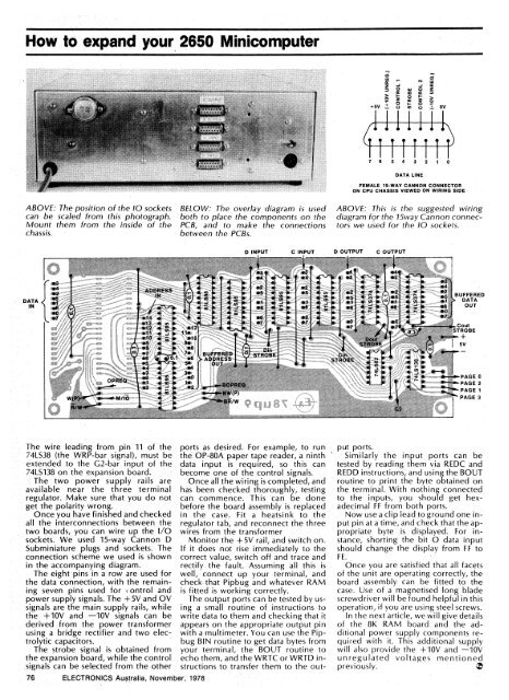
How to expand your <strong>2650</strong> Minicomputer<br />
ABOVE: <strong>The</strong> position of the 10 sockets<br />
can be scaled from this photograph.<br />
Mount them from the inside of the<br />
chassis.<br />
DATA<br />
IN<br />
Issionto<br />
<strong>The</strong> wire leading from pin 11 of the<br />
74LS38 (the WRP-bar signal), must be<br />
extended to the G2-bar input of the<br />
74LS138 on the expansion board.<br />
<strong>The</strong> two power supply rails are<br />
available near the three terminal<br />
regulator. Make sure that you do not<br />
get the polarity wrong.<br />
Once you have finished and checked<br />
all the interconnections between the<br />
two boards, you can wire up the I/O<br />
sockets. We used 15-way Cannon D<br />
Subminiature plugs and sockets. <strong>The</strong><br />
connection scheme we used is shown<br />
in the accompanying diagram.<br />
<strong>The</strong> eight pins in a row are used for<br />
the data connection, with the remaining<br />
seven pins used for t ontrol and<br />
power supply signals. <strong>The</strong> +5V and OV<br />
signals are the main supply rails, while<br />
the +10V and ---10V signals can be<br />
derived from the power transformer<br />
using a bridge rectifier and two electrolytic<br />
capacitors.<br />
<strong>The</strong> strobe signal is obtained from<br />
the expansion board, while the control<br />
signals can be selected from the other<br />
76 ELECTRONICS Australia, November, 1978<br />
BELOW: <strong>The</strong> overlay diagram is used<br />
both to place the components on the<br />
PCB, and to make the connections<br />
between the PCBs.<br />
+5V<br />
cc<br />
z<br />
0<br />
O<br />
cc<br />
z<br />
0<br />
D INPUT • C INPUT D OUTPUT C OUTPUT<br />
ports as desired. For example, to run<br />
the OP-80A paper tape reader, a ninth<br />
data input is required, so this can<br />
become one of the control signals.<br />
Once all the wiring is completed, and<br />
has been checked thoroughly, testing<br />
can commence. This can be done<br />
before the board assembly is replaced<br />
in the case. Fit a heatsink to the<br />
regulator tab, and reconnect the three<br />
wires from the transformer<br />
Monitor the +5V rail, and switch on.<br />
If it does not rise immediately to the<br />
correct value, switch off and trace and<br />
rectify the fault. Assuming all this is<br />
well, connect up your terminal, and<br />
check, that Pipbug and whatever RAM<br />
is fitted is working correctly.<br />
<strong>The</strong> output ports can be tested by using<br />
a small routine of instructions to<br />
write data to them and checking that it<br />
appears on the appropriate output pin<br />
with a multimeter. You can use the Pipbug<br />
BIN routine to get data bytes from<br />
your terminal, the BOUT routine to<br />
echo them, and the WRTC or WRTD instructions<br />
to transfer them to the out-<br />
La<br />
0<br />
cc<br />
0<br />
Q<br />
z<br />
0<br />
0<br />
z<br />
0<br />
OV<br />
1 •<br />
6 I I I I 1<br />
7 1 5 4 3 2 1 0<br />
DATA LINE<br />
FEMALE 15-WAY CANNON CONNECTOR<br />
ON CPU CHASSIS VIEWED ON WIRING SIDE •<br />
ABOVE: This is the suggested wiring<br />
diagram for the 15way Cannon connectors<br />
we used for the 10 sockets.<br />
BUFFERED<br />
DATA<br />
OUT<br />
Cout<br />
STROBE<br />
-I-<br />
5V<br />
PAGE 0<br />
.------,40441.-PAGE 2 -<br />
---:<br />
PAGE 1<br />
PAGE 3<br />
put ports.<br />
Similarly the input ports can be<br />
tested by reading them via REDC and<br />
REDD instructions, and using the BOUT<br />
routine to print the byte obtained on<br />
the terminal. With nothing connected<br />
to the inputs, you should get hexadecimal<br />
FF from both ports.<br />
Now use a clip lead to ground one input<br />
pin at a time, and check that the appropriate<br />
byte is displayed. For instance,<br />
shorting the bit 0 data input<br />
should change the display from FF to<br />
FE.<br />
Once you are satisfied that all facets<br />
of the unit are operating correctly, the<br />
board assembly can be fitted to the<br />
case. Use of a magnetised long blade<br />
screwdriver will be found helpful in this<br />
operation, if you are using steel screws.<br />
In the next article, we will give details<br />
of the 8K RAM board and the additional<br />
power supply components required<br />
with it. This additional supply<br />
will also provide the +10V and —10y<br />
unregulated voltages mentioned<br />
previously.