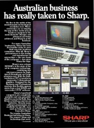
The Signetics 2650 - The MESSUI Place
The Signetics 2650 - The MESSUI Place
The Signetics 2650 - The MESSUI Place

You also want an ePaper? Increase the reach of your titles
YUMPU automatically turns print PDFs into web optimized ePapers that Google loves.
tends to introduce hassles when you try<br />
to use certain 5-100 boards. <strong>The</strong> choice<br />
is up to you.<br />
Of course, some of the 5-100 control<br />
signals are more important than others.<br />
Some signals are only needed if you<br />
plan to have a fancy front panel on your<br />
system — a feature which is not as popular<br />
nowadays as it was. Others are only<br />
used for things like a hardwareimplemented<br />
single step facility, or<br />
stack management hardware external<br />
to the processor. If you don't want<br />
these facilities, or don't need them,<br />
then the signals can be ignored.<br />
Perhaps the remaining general point<br />
that should be made about the S-100<br />
bus is that as you can see, it uses two 8bit<br />
data buses: one for data into the<br />
processor, and the other for data out of<br />
the processor. This is a carryover from<br />
the original Altair design, and is again a<br />
little clumsy by modern standards. In<br />
general only one of the two buses is<br />
ever in use at any instant, so it would be<br />
more elegant and efficient to have a<br />
single bidirectional bus.<br />
But if you want to make your interface<br />
compatible with most of the 5-100<br />
plug-ins, you have to provide for the<br />
two separate data buses — clumsy<br />
though they may be. Of course you can<br />
always provide your own bidirectional<br />
bus as well, using eight of the unstandardised<br />
pins. Just make sure that the<br />
pins you use aren't needed by any of<br />
your S-100 plug-ins for special control<br />
signals.<br />
Well then, let's get down to specifics.<br />
What's involved in providing an 5-100<br />
interface for your <strong>2650</strong> Mini Computer<br />
system?<br />
Before going any further, I would like<br />
to stress that the remainder of this article<br />
consists basically of a set of<br />
suggestions, rather than the description<br />
of an interface that has been built up<br />
and tested. <strong>The</strong> circuit diagram given<br />
has not been tested, as this would have<br />
involved a considerable amount of time<br />
and effort which could not really be<br />
justified in view of the limited interest.<br />
But it has been prepared from a careful<br />
survey of 5-100 literature and reference<br />
material, and I believe it to be fully<br />
practical.<br />
Basically if you want to provide your<br />
<strong>2650</strong> system with an S-100 interface<br />
which provides each and every one of<br />
the various standardised control<br />
signals, it isn't easy. But on the other<br />
hand, some of the control signals turn<br />
out to be unnecessary in a <strong>2650</strong>-based<br />
system, except in very rare circumstances.<br />
<strong>The</strong> interface shown in the circuit<br />
diagram provides only the main control<br />
signals, but should be suitable for interfacing<br />
your <strong>2650</strong> system to most S-100<br />
plug-ins.<br />
Let's run through the circuit, starting<br />
from the bottom and working upward.<br />
First are the 16 address lines ADO-AD15,<br />
buffered by a pair of 81L595 or similar<br />
Tri-state octal buffers. <strong>The</strong> inputs for<br />
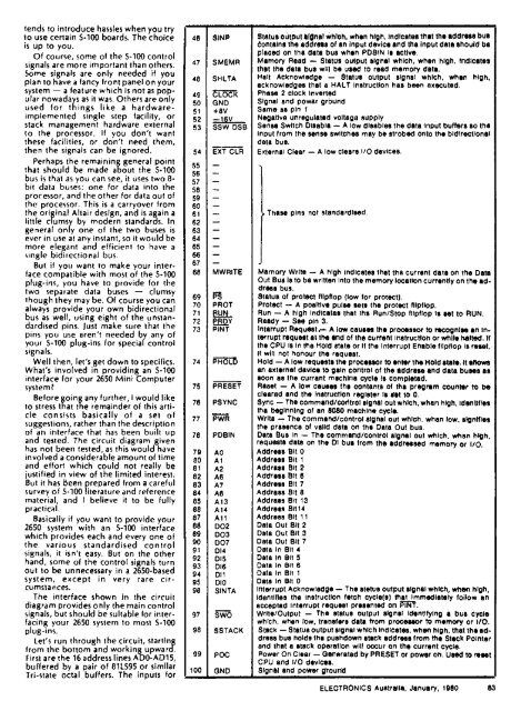
48 SINP Status output Signal which, when high, Indfcates that the address bus<br />
Contains the address of an Input device and the Input date should be<br />
placed on the data bus when PDBIN Is active.<br />
47 SMEMR Memory Read — Status output signal which, when high. Indicates<br />
that the data bus will be used to read memory data.<br />
48 SHLTA Halt Acknowledge — Status output signal which, when high,<br />
acknowledges that a HALT instruction has been executed.<br />
49 ILO Phase 2 clock inverted<br />
50 GND Signal end power grOund<br />
51 +8V Same as pin 1<br />
52 =16‘.! Negative unregulated voltage supply<br />
53 SSW DSB Sense Switch Disable — A low disables the data input buffers so the<br />
Input from the sense switches may be strobed onto the bidirectional<br />
data bus.<br />
54 EXT CLR External Clear — A low clears I/O devices.<br />
55<br />
56<br />
57<br />
58<br />
59<br />
60<br />
61<br />
<strong>The</strong>se pins not standardised.<br />
62<br />
63<br />
64<br />
65<br />
66<br />
67<br />
68 MWRITE Memory Write — A high indicates that the current data on the Date<br />
Out Bus Is to be written into the memory location currently on the ad-<br />
dress bus.<br />
69 Status of protect flpflop (low for protect).<br />
70 PROT Protect — A positive pulse sets the protect filpflop.<br />
71 RUN Run — A high indicates that the Run/Stop filpflop Is set to RUN.<br />
72 eaa Ready — See pin 3.<br />
73 PINT Interrupt Request.— A low causes the processor to recognise en in-<br />
terrupt request at the end of the current Instruction or while halted. If<br />
the CPU Is In the Hold state or if the Interrupt Enable MAIN) is reset.<br />
It will not honour the request.<br />
74 PF=1 Hold — A low requests the processor to enter the Hold state. It allows<br />
an external device to gain control of the address end data buses as<br />
soon as the current machine cycle is completed.<br />
75 PRESET Reset — A low causes the contents of the program counter to be<br />
cleared and the instruction register is Set to 0.<br />
78 PSVNC Sync — <strong>The</strong> command/control signal out which, when high, Identifies<br />
the beginning of an 8080 machine cycle.<br />
77 PWR Write -7 the command/control signal out which, when low, signifies<br />
the presence of valid date on the Data Out bus.<br />
78 PDBIN Data Bus in — <strong>The</strong> commend/control signal out which, when high.<br />
requests data on the DI bus from the addressed memory or I/O.<br />
79 AO Address Bit 0<br />
80 Al Address Bit .l<br />
81 A2 Address Bit 2<br />
82 AS Address Bit 6<br />
83 A7 Address Bit 7<br />
84 A8 Address Bit 8<br />
85 A13 Address Bit 13<br />
86 A14 Address Bit14<br />
87 All Address Bit 11<br />
88 DO2 Data Out Bit 2<br />
B9 DO3 Data Out Bit 3<br />
90 007 Data Out Bit 7<br />
91 014 Data In Bit 4<br />
92 015 Data in Bit 5<br />
93 D16 Data in Bit 8<br />
94 Dil Data in Bit 1<br />
95 DIO Date In Bit 0<br />
96 SINTA Interrupt Acknowledge — <strong>The</strong> status output signal which, when high,<br />
Identifies the instruction fetch owlets) that Immediately follow en<br />
accepted Interrupt request presented on Wt.<br />
97 SWO Write/Output — <strong>The</strong> statue output signal Identifying a bus cycle<br />
which. when low, transfers data from processor to memory or I/O.<br />
98 SSTACK Stack — Status output signal which indicates, when high, that the ad-<br />
dress bus holds the pushdown stack eddress from the Steck Pointer<br />
and that a stack operation will occur on the current cycle.<br />
99 POC Power On Clear — Generated by PRESET or power on. Used to reset<br />
CPU and I/O devices.<br />
100 GND Signet and power ground<br />
ELECTRONICS Australia, January, 1980 83