The Signetics 2650 - The MESSUI Place
The Signetics 2650 - The MESSUI Place
The Signetics 2650 - The MESSUI Place

Create successful ePaper yourself
Turn your PDF publications into a flip-book with our unique Google optimized e-Paper software.
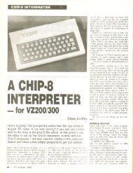
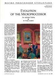
84 ELECTRONICS Australia, January, 1980<br />
the buffers are taken from the address<br />
lines (already buffered) on the <strong>2650</strong><br />
Mini Computer's expansion board. —<br />
Note that the S-100 bus requires 16<br />
address lines, whereas the <strong>2650</strong> system<br />
only has 15 lines available (ADO-AD14).<br />
<strong>The</strong> input of the 16th buffer is therefore<br />
tied permanently to ground.<br />
One enable input of each of the<br />
811595 address buffer devices is connected<br />
to a gate. This allows the buffers<br />
to be disabled, and the 5-100 address<br />
lines to be floated in a high Impedance<br />
state, either in response to the<br />
ADD DSB-bar signal (pin 22) or when<br />
the processor is halted. Other 5-100<br />
boards are thus able to take control of<br />
the address lines, for things like DMA<br />
(direct memory access) data transfers.<br />
Moving upward, we find two more<br />
81L595 octal buffers, the first used to<br />
buffer the 5-100 data out lines 000-<br />
D07, and the second to buffer the 5-<br />
100 data input lines DIO-D17. As with<br />
the address buffers, the data out buffers<br />
are controlled by another gate, so they<br />
can be disabled either in response to<br />
the DO DSB-bar signal (pin 23) or when<br />
the processor is halted.<br />
In addition, both the DO and DI<br />
buffers are controlled separately by two<br />
of the outputs of an 825103 device. This<br />
is a programmable gate array, which<br />
<strong>Signetics</strong> and Philips are making<br />
available pre-programmed with the<br />
logic functions necessary to generate<br />
eight key 5-100 control signals from the<br />
existing <strong>2650</strong> control signals OPREQ, Rbar/W,<br />
M/I0-bar and WRP.<br />
As you can see, besides the two data<br />
buffer control signals the device also<br />
produces the S-100 signals SOOT (pin<br />
45), SINP (pin 46), SMEMR (pin 47),<br />
PWR-bar (pin 77), PDBIN (pin 78) and<br />
MWRT (pin 68). So it really takes some<br />
of the hassles out of making the <strong>2650</strong><br />
"pretend" to be an 8080!<br />
<strong>The</strong> preprogrammed version of the<br />
825103 is coded with the suffix CK1179,<br />
and is available from your normal parts<br />
supplier on order from Philips Industries.<br />
It should cost you less than<br />
$10, including tax.<br />
<strong>The</strong> programming chart for the<br />
825103/0(1179 is shown in Table 2, for<br />
the benefit of those who want to<br />
analyse the logic functions involved in<br />
producing the S-100 signals. Note that<br />
device inputs 14, 15 and IF are not used,<br />
and can be left unconnected; similarly<br />
the ninth device output F8 is not used.<br />
Note also that inputs 16 to IE inclusive<br />
are all effectively programmed to act as<br />
active-high enable inputs, so that they<br />
must all be taken to logic high level for<br />
any output to be enabled.<br />
What this means is that these inputs<br />
may effectively be used to disable the<br />
5-100 interface, whenever the<br />
processor is dealing with the memory<br />
and I/O ports provided in the original<br />
<strong>2650</strong> system. This is done simply by connecting<br />
active-low enable signals from<br />
the existing <strong>2650</strong> system to some of the<br />
825103 enable inputs, as shown. <strong>The</strong><br />
remaining enable inputs are simply tied