plasma tv service manual
plasma tv service manual
plasma tv service manual

Create successful ePaper yourself
Turn your PDF publications into a flip-book with our unique Google optimized e-Paper software.
8. Tool Option Area Option Change<br />
8-1. Profile<br />
: Must be changed the option value because being different with<br />
some setting value depend on module, inch and market.<br />
8-2. Required Test Equipment<br />
1) Adjustment remocon.<br />
8-3. Adjustment method<br />
Before PCB check, have to change the Tool option and Area option.<br />
Option values are below.<br />
(If on changed the option, the input menu can differ the model spec.)<br />
The input methods are same as other chassises.(Use adj Key<br />
on the Adjust Remocon)<br />
42<br />
TOOL OPTION ZA/ZB TA/TB<br />
PC5R(PC51) 2244<br />
4292<br />
PC6R<br />
2500<br />
4548<br />
VGA<br />
PC7R<br />
2756<br />
4804<br />
PB3R<br />
3012<br />
5060<br />
PC5R(PC51) 2252<br />
4300<br />
PC6R<br />
2508<br />
4556<br />
XGA<br />
PC7R<br />
2764<br />
4814<br />
PB3R<br />
3020<br />
5068<br />
* After done all adjustments, Press ADJ button and compare<br />
Tool option and Area option value with its BOM, if it is<br />
correctly same then unplug the AC cable.<br />
If it is not same, then correct it same with BOM and unplug AC cable.<br />
For correct it to the model’s module from factory JIG model.<br />
9. Color carrier Adjustment<br />
(Inspection process)<br />
9-1. Profile<br />
: To have the margin about the deviation of color carrier to<br />
satisfy the spec.<br />
9-2. Required Test Equipment<br />
1) Adjustment remocon.<br />
2) Pal RF signal.<br />
9-3. Connection<br />
: TV set should connected with the pal RF signal(EU 5CH).<br />
9-4. Adjustment method<br />
(1) tuning the RF signal<br />
ZA/ZB, TA/TB : PAL Philips Pattern (with Color Bar)<br />
(2) push the “adj” key in the adjustment remocon.<br />
- 11 -<br />
Each PCB assembly must be checked by check JIG set.<br />
(Because power PCB Assembly damages to PDP Module,<br />
especially be careful)<br />
10. POWER PCB Assy Voltage<br />
Adjustments (Va, Vs Voltage adjustments)<br />
10-1. Profile<br />
: To supply the Va, Vs voltage that the module want.<br />
10-2. Required Test Equipment<br />
(1) Stick for adjustment.<br />
(2) DMM.<br />
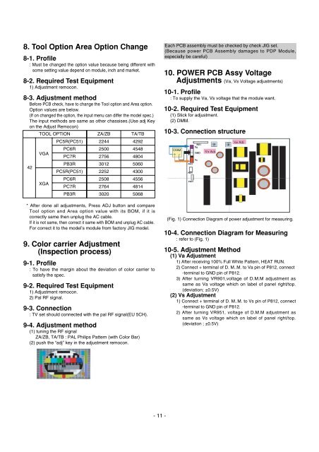
10-3. Connection structure<br />
(Fig. 1) Connection Diagram of power adjustment for measuring.<br />
10-4. Connection Diagram for Measuring<br />
: refer to (Fig. 1)<br />
10-5. Adjustment Method<br />
(1) Va Adjustment<br />
1) After receiving 100% Full White Pattern, HEAT RUN.<br />
2) Connect + terminal of D. M..M. to Va pin of P812, connect<br />
-terminal to GND pin of P812.<br />
3) After turning VR901,voltage of D.M.M adjustment as<br />
same as Va voltage which on label of panel right/top.<br />
(deviation; ±0.5V)<br />
(2) Vs Adjustment<br />
1) Connect + terminal of D. M..M. to Vs pin of P812, connect<br />
-terminal to GND pin of P812.<br />
2) After turning VR951, voltage of D.M.M adjustment as<br />
same as Vs voltage which on label of panel right/top.<br />
(deviation ; ±0.5V)