FM-TX2-XXX FM-RX2-XXX - Netzmafia
FM-TX2-XXX FM-RX2-XXX - Netzmafia
FM-TX2-XXX FM-RX2-XXX - Netzmafia

Create successful ePaper yourself
Turn your PDF publications into a flip-book with our unique Google optimized e-Paper software.
<strong>FM</strong> TRANSMITTER & RECEIVER <strong>FM</strong>-<strong>TX2</strong>-<strong>XXX</strong><br />
MODULES. (2ND GENERATION) <strong>FM</strong>-<strong>RX2</strong>-<strong>XXX</strong><br />
Functional description:<br />
The <strong>TX2</strong> transmitter module is a two stage, SAW controlled <strong>FM</strong> transmitter operating between<br />
2V and 6V and is available in 433.92MHz and 418.00 MHz versions. The 433.92 MHz unit is<br />
type-approved to ETS 300-220 for European use and delivers nominally +9dBm from a 5V<br />
supply at 12mA, while the 418.00 MHz unit has MPT 1340 type-approval for U.K. use and<br />
delivers -3dBm from a 5V supply at 5mA. Both modules measure 12 x 32 x 3.8 mm.<br />
The <strong>RX2</strong> module is a double conversion <strong>FM</strong> superhet receiver capable of handling date rates of<br />
upto 40kbit/s. The SIL style <strong>RX2</strong> receiver measures 17.5 x 48 x 4.5 mm. It will operate from a<br />
supply of 3-6V and draws 14mA when receiving. A fast-acting carrier detect and a power-up<br />
enable time of less than 1ms This allows effective duty cycle power saving and a -107 dBm<br />
sensitivity. This, combined with a SAW front-end filter results in an excellent RF performance<br />
and EMC conformance.<br />
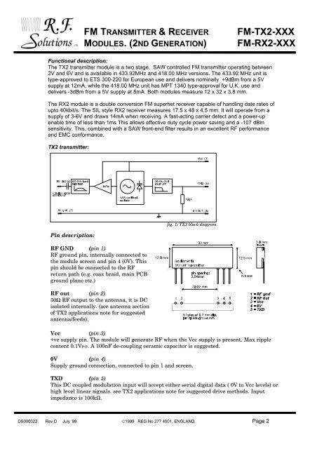
<strong>TX2</strong> transmitter:<br />
Pin description:<br />
RF GND (pin 1)<br />
RF ground pin, internally connected to<br />
the module screen and pin 4 (0V). This<br />
pin should be connected to the RF<br />
return path (e.g. coax braid, main PCB<br />
ground plane etc.)<br />
RF out (pin 2)<br />
50Ω RF output to the antenna, it is DC<br />
isolated internally. (see antenna section<br />
of <strong>TX2</strong> applications note for suggested<br />
antenna/feeds).<br />
fig. 1: <strong>TX2</strong> block diagram<br />
Vcc (pin 3)<br />
+ve supply pin. The module will generate RF when the Vcc supply is present. Max ripple<br />
content 0.1VP-P. A 100nF de-coupling ceramic capacitor is suggested.<br />
0V (pin 4)<br />
Supply ground connection, connected to pin 1 and screen.<br />
TXD (pin 5)<br />
This DC coupled modulation input will accept either serial digital data ( 0V to Vcc levels) or<br />
high level linear signals. see <strong>TX2</strong> applications note for suggested drive methods. Input<br />
impedance is 100kΩ.<br />
DS000022 Rev D July ‘99 ©1999 REG No 277 4001, ENGLAND. Page 2