AN1307 Application Note - Netzmafia
AN1307 Application Note - Netzmafia
AN1307 Application Note - Netzmafia

You also want an ePaper? Increase the reach of your titles
YUMPU automatically turns print PDFs into web optimized ePapers that Google loves.
SEMICONDUCTOR APPLICATION NOTE<br />
<br />
<br />
Prepared by: Denise Williams<br />
Discrete <strong>Application</strong>s Engineering<br />
Semiconductor pressure transducers offer an economical<br />
means of achieving high reliability and performance in<br />
pressure sensing applications. The completely integrated<br />
MPX5100 (0–15 PSI) series pressure transducer provides a<br />
temperature–compensated and calibrated, high–level linear<br />
ICePAK and SENSEFET are trademarks of Motorola, Inc.<br />
REV 1<br />
Motorola Sensor Device Data<br />
© Motorola, Inc. 1997<br />
INTRODUCTION<br />
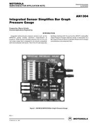
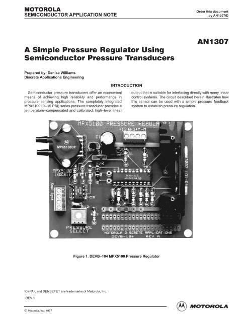
Figure 1. DEVB–104 MPX5100 Pressure Regulator<br />
Order this document<br />
by <strong>AN1307</strong>/D<br />
<br />
output that is suitable for interfacing directly with many linear<br />
control systems. The circuit described herein illustrates how<br />
this sensor can be used with a simple pressure feedback<br />
system to establish pressure regulation.<br />
1
MPX2XXX<br />
+5 V<br />
3 2<br />
4 1<br />
RG<br />
IC1 — MC33079<br />
RG — 10K POT<br />
3<br />
2<br />
1M<br />
1M<br />
6<br />
5<br />
+<br />
–<br />
4<br />
IC1A<br />
IC1B<br />
11<br />
1<br />
7<br />
Figure 2. High Level, Ground Referenced Output Using an MPX2000 Series Transducer<br />
The MPX5100 is the next level of integration beyond the<br />
MPX2000 series. The MPX2000 series of pressure<br />
transducers already incorporates, on–chip, more than a<br />
dozen external components needed for temperature<br />
compensation and offset calibration. Figure 2 shows the basic<br />
circuitry required to create a ground referenced output<br />
amplified to a high–level from an MPX2100 (0–15 PSI)<br />
transducer. For optimum performance, matched metal film<br />
resistor pairs and precision operational amplifiers are<br />
required.<br />
The MPX5100 goes one step further by adding the<br />
differential to ground referenced conversion and the<br />
amplification circuitry on–chip. Therefore, the<br />
eighteen–component circuit shown in Figure 2 can be reduced<br />
to one signal–conditioned sensor, as shown in Figure 3.<br />
All of the MPX devices contain a single piezoresistive<br />
implant which replaces the four–element Wheatstone bridge<br />
circuit found in most semiconductor–based transducers. The<br />
MPX5100 transducer uses an interactively laser–trimmed,<br />
four–stage network to perform signal conditioning. Figure 4 is<br />
an internal block diagram of the MPX5100 showing these four<br />
stages.<br />
–<br />
+<br />
C1<br />
THE SENSOR<br />
2 Motorola Sensor Device Data<br />
100K<br />
100K<br />
100K<br />
10<br />
9<br />
100K<br />
+<br />
–<br />
100K<br />
14<br />
IC1C<br />
IC1D<br />
8<br />
10K<br />
–<br />
+<br />
13<br />
12<br />
+5 V<br />
2K<br />
10K<br />
2K<br />
Vout<br />
The first stage compensates for the temperature coefficient<br />
of offset while the second stage performs the differential to<br />
single–ended conversion. Stage three is a precision voltage<br />
reference that calibrates the zero pressure offset of the entire<br />
system, which comprises the sensor offset and the input offset<br />
voltages of the other three operational amplifiers. The final<br />
stage provides the full–scale span calibration. The MPX5100<br />
is compensated for operation over 0 to 85°C with a response<br />
time (10% to 90%) of 1.0 msec.<br />
+5 V<br />
3<br />
1<br />
2<br />
Vout<br />
Figure 3. High Level, Ground Referenced<br />
Output Using an MPX5100
Vex<br />
RS<br />
V1<br />
R1<br />
R2<br />
PIN 2<br />
RTO<br />
VS–<br />
Motorola Sensor Device Data<br />
V2<br />
R3<br />
OA1<br />
VS+<br />
Some terms commonly used when discussing pressure<br />
sensors are:<br />
• VFSS (Full Scale Span) — the output voltage variation between<br />
zero differential pressure applied to the sensor and<br />
the maximum recommended operating pressure applied to<br />
the sensor, with a given supply voltage.<br />
• VOFF (Offset) — the voltage output given by a sensor with<br />
zero differential pressure applied, with a given supply voltage.<br />
• Sensitivity — the amount of output voltage variation per<br />
unit pressure input variation.<br />
• Linearity — the maximum deviation of the output from a<br />
straight line relationship over the operating pressure range.<br />
–<br />
+<br />
VA<br />
R4<br />
R5<br />
R11<br />
R9 R10<br />
R13<br />
Figure 4. Fully Integrated Pressure Sensor Schematic<br />
V3<br />
VP<br />
V4<br />
– OA4<br />
OA2<br />
+<br />
+<br />
R8<br />
THIN FILM RESISTOR<br />
LASER TRIMMABLE RESISTOR<br />
–<br />
PIN 3<br />
+5 V SOURCE<br />
RG<br />
Q4<br />
QOUT<br />
<br />
PIN 1<br />
VOUT<br />
Motorola specifies linearity using an “end–point straight<br />
line” method.<br />
Each transducer is laser trimmed to provide the specified<br />
VFSS with the supply voltage indicated on the data sheet. For<br />
example, VFSS for the MPX5100 is trimmed to 4.0 V with a<br />
supply voltage of +5.0 Vdc.<br />
For the MPX5100, VOFF = 0.5 V with a 5.0 Vdc supply.<br />
Therefore, the output of the sensor varies from 0.5 V to 4.5 V<br />
for differential pressures from 0 kPa to 100 kPa, respectively.<br />
This is ideal for interfacing directly with many linear devices<br />
such as the MC33033 motor controller described in this<br />
application note or the A/D of a microprocessor controlled<br />
system.<br />
3
Figure 5 is a block diagram of a simple pressure regulator<br />
feedback system. The motor/pump is used to fill a reservoir as<br />
required. The pressure created in this reservoir is monitored<br />
with a gauge and fed back to the MPX5100 sensor. The sensor<br />
provides an output voltage to the Motor Drive Circuitry which<br />
is proportional to the monitored pressure.<br />
PRESSURE<br />
PORT<br />
SENSOR<br />
PRESSURE<br />
SELECT<br />
CIRCUITRY<br />
+12 Vdc<br />
GND<br />
3<br />
1<br />
2<br />
MOTOR<br />
DRIVE<br />
CIRCUITRY<br />
MOTOR/PUMP<br />
Figure 5. System Block Diagram<br />
+ C1<br />
220<br />
Sout<br />
XDCR1<br />
MPX5100<br />
FWD/REV<br />
S1<br />
R11<br />
3900<br />
R12<br />
10K<br />
R13<br />
330<br />
Sgnd<br />
R5<br />
10K<br />
3<br />
IC2<br />
78L05<br />
VI G<br />
N<br />
VO 1<br />
D C4<br />
2<br />
1.0<br />
C2<br />
0.005<br />
R8<br />
10K<br />
3<br />
2<br />
MC33033<br />
BRUSHLESS<br />
MOTOR CONTROLLER<br />
+<br />
–<br />
1<br />
2<br />
3<br />
4<br />
5<br />
6<br />
7<br />
8 9<br />
10<br />
+12<br />
8<br />
IC1<br />
BT<br />
AT<br />
F/R<br />
HA<br />
HB<br />
HC<br />
REF<br />
OSC<br />
+<br />
–<br />
300K<br />
C5<br />
0.01<br />
1<br />
IC3A<br />
4 MC34272<br />
CT EP<br />
AB<br />
BB<br />
CB<br />
VCC<br />
GND<br />
CL<br />
EA<br />
R10<br />
20<br />
19<br />
18<br />
17<br />
16<br />
15<br />
14<br />
13<br />
12<br />
11<br />
ÅÅÅÅ<br />
ÅÅÅÅ<br />
RESERVOIR<br />
ÅÅÅÅ<br />
R9<br />
10K<br />
THE CIRCUIT<br />
R3<br />
470<br />
C3<br />
0.001<br />
R1<br />
Figure 6. MPX5100 Pressure Regulator<br />
1K<br />
The Pressure Select Circuitry allows the user to choose a<br />
desired pressure by creating a reference voltage. This<br />
reference voltage is equivalent to the sensor output when the<br />
desired pressure exists in the system. A comparison is made<br />
between the sensor output and the reference voltage. When<br />
the system pressure is below the selected pressure, the motor<br />
is turned on to increase the pressure. When the system<br />
pressure reaches the selected pressure, the motor/pump<br />
turns off. Hysteresis is used to set different trip voltages for<br />
turn–off and turn–on to allow for noise and pressure<br />
fluctuations.<br />
For particular applications that only require one fixed<br />
regulated pressure, the Pressure Select Circuitry can be<br />
reduced to a single voltage reference. Additionally, the Motor<br />
Drive Circuitry can be simplified depending on the application<br />
requirements and the motor to be used. Since a +5.0 Vdc<br />
supply to the sensor provides an output that is ideal for<br />
interfacing with an A/D converter, this comparison could<br />
easily be converted to a software function, allowing for a digital<br />
pressure select input as well as controlling a digital display.<br />
Q1<br />
1/4 MPM3002<br />
Q3<br />
1/4 MPM3002<br />
47<br />
R4<br />
R7 47<br />
4 Motorola Sensor Device Data<br />
R6<br />
24<br />
R2<br />
470<br />
Q2<br />
1/4 MPM3002<br />
MOTOR +<br />
MOTOR –<br />
Q4<br />
1/4 MPM3002
The Supply Voltage<br />
Figure 6 is a schematic of the control electronics for this<br />
pressure regulator system. The +12 Vdc supply is used by the<br />
MPM3002 power transistors, the MC33033 motor controller<br />
and the MC34272 operational amplifier. In addition, this<br />
voltage is regulated down to +5.0 Vdc for the sensor supply.<br />
The Pressure Select Circuitry<br />
R11, R12 and R13 provide a variable reference from 0.5 V<br />
to 4.5 V. By adjusting R12, the reference voltage can be set to<br />
the desired pressure turn–off point. The error amplifier internal<br />
to the MC33033, along with R8, R9 and R10, is configured as<br />
a comparator with hysteresis. The sensor output voltage and<br />
the reference voltage are inputs to the comparator and are<br />
used to determine when the motor is turned on or turned off.<br />
When the sensor output is less than the reference voltage the<br />
motor is on. Pressure in the system increases until the sensor<br />
output is equal to the reference voltage plus the hysteresis<br />
voltage then the motor is turned off. If the pressure decreases<br />
while the motor is off, the sensor output will decrease until it<br />
is equal to the reference voltage at which time the motor turns<br />
on.<br />
Hysteresis is set to prevent the motor from turning off and<br />
on due to small voltage variations such as noise or small<br />
pressure fluctuations in the system. The ratio of R10 to both<br />
R8 and R9 can be adjusted to provide the hysteresis required<br />
in a particular application. The resistor values shown in Figure<br />
6 provide a ratio of 300 kΩ to 10 kΩ. This corresponds to a<br />
hysteresis of 300 mV or 7.5 kPa between the turn–off and<br />
turn–on trip points. The operational amplifier (MC34272) is<br />
used to provide a low impedance output to isolate the divider<br />
network from the comparator circuit.<br />
The Motor Drive Circuitry<br />
In a brush motor drive, the primary function of the controller<br />
IC is to translate speed and direction inputs into appropriate<br />
drive for the power transistors. This can be done efficiently by<br />
using the MC33033 Brushless DC controller as shown in<br />
Figure 6. In a brushless application, two of six output<br />
transistors are switched on in response to Hall sensor inputs<br />
HA, HB and HC. In order to drive a brush motor, all that is<br />
required is to select a single Hall code that will drive a four<br />
transistor H–bridge in a way that is suitable for brush motors.<br />
By using phase A and phase C outputs, a 1–0–0 Hall code<br />
produces the correct drive for brush motors. AT, BT and CT are<br />
open collector outputs, therefore, a logic 0 represents the on<br />
state. Conversely, AB, BB and CB are totem pole drivers, and<br />
a logic 1 turns on the corresponding output transistor.<br />
Generating the Hall code is easy. Since it is fixed at 1–0–0,<br />
tying the Hall inputs to DC levels is sufficient. Logic 1 is<br />
obtained from VREF, and logic 0 from ground. The result is the<br />
Motorola Sensor Device Data<br />
DETAILED CIRCUIT DESCRIPTION<br />
<br />
connections for pins 4, 5 and 6 that are shown in Figure 6. In<br />
addition to providing drive to the output transistors, the<br />
MC33033 has a current limit function and controls speed by<br />
pulse width modulating the lower output transistors, Q3 and<br />
Q4. The current limit operates on a 100 mV threshold. Once<br />
tripped, it latches the lower transistor drive off until the next<br />
clock cycle begins. The latching feature prevents high<br />
frequency oscillations which would otherwise overheat the<br />
power transistors. Compatibility with SENSEFETs is<br />
provided by the 100 mV threshold and allows the lossless<br />
current sensing configuration that is also shown in Figure 6.<br />
For low–power, low–voltage motors, level shifting the<br />
gate–drain for Q1 and Q2, the upper output transistors, is not<br />
a problem. Open collector top–side outputs in the MC33033<br />
interface directly to P–Channel MOSFETs. All that is required<br />
in the way of top–side drive circuitry is gate–to–source<br />
resistors on the P–Channel transistors, such as R2 and R3 in<br />
Figure 6.<br />
Since an H–Bridge motor drive uses four power transistors,<br />
a power module can considerably simplify the output stage.<br />
The MPM3002 that is shown as Q1, Q2, Q3 and Q4 in Figure<br />
6 is ideally suited to fractional horsepower motor drives. It<br />
consists of two P–Channel MOSFETs and two N–Channel<br />
SENSEFETs connected in an H–Bridge configuration, and<br />
housed in an isolated 12–pin, single, in–line package. The<br />
P–Channels have a maximum on–resistance of 0.4 ohms, and<br />
the N–Channels 0.15 ohms. All four transistors have 100 V<br />
breakdown ratings.<br />
The MPM3002’s P–Channel/N–Channel configuration<br />
makes interfacing to an MC33033 control IC especially easy.<br />
The schematic shows an example. The SENSEFETs are<br />
connected to outputs AB and CB through series gate resistors,<br />
and the P–Channels are connected directly to AT and CT and<br />
tied to the +12 V rail through pull–up resistors. If the source<br />
voltage is greater than +12 V, a divider can be used to keep<br />
gate voltage on the P–Channels within reasonable limits.<br />
In the schematic, the mirror outputs of both SENSEFETs are<br />
tied together. They are then fed into the MC33033’s current<br />
limit input through a noise suppression filter consisting of R7<br />
and C3. Since only one SENSEFET is on at any given time,<br />
this connection is a logic wired–OR. It provides overcurrent<br />
protection for both directions of motor rotation, and does not<br />
alter trip points for the individual legs. The trip point is<br />
calculated with the aid of the following expression.<br />
ILIMIT=VSENSE (RSENSE – rm(on))/(ra(on)⋅RSENSE)<br />
Where:<br />
VSENSE is sense voltage<br />
RSENSE is the mirror–to–source sense resistor<br />
rm(on) is mirror–active resistance = 112 ohms<br />
ra(on) is source–active resistance = 0.14 ohms<br />
5
MPX5100<br />
(XDCR1)<br />
Sout Sgnd<br />
S1<br />
F/R<br />
R8 R11 R9 R1<br />
0<br />
MPX5100 PRESSURE REGULATOR<br />
+12 GND+M–M<br />
C1<br />
IC2<br />
IC3<br />
C5 R12<br />
R13<br />
+<br />
C2 R5 R3<br />
MC33033<br />
C3 R6 C4 R7 R4 R1 R2<br />
PRESSURE<br />
SELECT MOTOROLA DISCRETE APPLICATIONS<br />
DEVB–104 REV A<br />
IC1<br />
Figure 7. PCB Component<br />
Layout<br />
Figure 9. PCB Solder<br />
Side Artwork<br />
Since the current limit threshold in the MC33033 is 100 mV,<br />
current limiting will occur when VSENSE reaches 100 mV. For<br />
the circuit in Figure 6, using 100 mV for VSENSE, and with<br />
RSENSE = R6 = 24 ohms then:<br />
ILIMIT = 0.1(24 +112)/(0.14⋅24) = 4.1 Amps<br />
By using SENSEFETs in the lower half bridge in lieu of a<br />
power sense resistor in series with the motor, about 1/2 watt<br />
(4.1 A⋅0.1 V) of dissipation is saved.<br />
MPM3002 (Q1–Q4)<br />
Figure 8. PCB Component<br />
Side Artwork<br />
Figures 7, 8, and 9 show a printed circuit board and<br />
component layout for the electronics portion of this pressure<br />
regulator system, and Table 1 is the corresponding parts list.<br />
System Performance<br />
The entire system draws 4.0 Amps with all but 50 mA used<br />
to drive the motor/pump. The pressure sensor provides a<br />
sensitivity to regulate well within a few kPa. However, most<br />
applications can allow far greater fluctuations in pressure. The<br />
system performance, therefore, depends mostly on the<br />
motor/pump selected and the hysteresis set in the control<br />
circuitry. Using a well–sealed pump will help ensure the motor<br />
turns off when the desired pressure is reached. Many pumps<br />
are designed to leak to prevent over inflation. In this case, the<br />
circuit will turn the motor off until the pressure is reduced,<br />
through leakage, by the designed hysteresis amount, then<br />
turn on and continue cycling to hold the pressure in the desired<br />
range.<br />
6 Motorola Sensor Device Data
S1<br />
Motorola Sensor Device Data<br />
Table 1. Parts List for Pressure Regulator PC Board<br />
Reference Designator Qty Description Comments<br />
R1, R4<br />
R2, R3<br />
R5, R8, R9<br />
R6<br />
R7<br />
R10<br />
R11<br />
R13<br />
1<br />
2<br />
1<br />
4<br />
6<br />
2<br />
1<br />
2<br />
2<br />
3<br />
1<br />
1<br />
1<br />
1<br />
1<br />
R12 1<br />
IC1<br />
IC2<br />
IC3<br />
Q1–Q4<br />
1<br />
1<br />
1<br />
1<br />
XDCR1 1<br />
C1<br />
C2<br />
C3<br />
C4<br />
C5<br />
CONCLUSION<br />
MISCELLANEOUS<br />
PC Board<br />
Input/Output Terminals<br />
Heat Sink<br />
1/2″ nylon standoffs, threaded<br />
1/2″ nylon screws<br />
4–40 nylon nuts<br />
switch<br />
RESISTORS, FIXED<br />
Comp., ±5%, 1/4 W<br />
47 Ω<br />
470 Ω<br />
10 kΩ<br />
24 Ω<br />
1 kΩ<br />
300 kΩ<br />
3900 Ω<br />
330 Ω<br />
See Figures 7–9<br />
PHX CONT #1727036<br />
for ICePAK<br />
SS–12SDP2<br />
RESISTORS, VARIABLE<br />
10 kΩ, one turn 3386P–1–103–T<br />
INTEGRATED CIRCUITS<br />
Motor Controller<br />
Reference<br />
Operational Amplifier<br />
Integrated H–Bridge<br />
SENSOR<br />
MPX5100DP<br />
This circuit is one example of how the MPX5100 with its<br />
high level output can directly interface with linear systems. It<br />
provides a simple design alternative where pressure<br />
measurement or control is required.<br />
1<br />
1<br />
1<br />
1<br />
1<br />
CAPACITORS<br />
220 μF, 25 V<br />
0.005 μF, ceramic, 25 V<br />
0.001 μF, ceramic, 25 V<br />
1 μF, ceramic, 50 V<br />
0.01 μF, ceramic, 25 V<br />
MC33033P<br />
78L05<br />
MC33272P<br />
MPM3002<br />
REFERENCE<br />
<br />
1. Schultz, Warren. “ICs Simplify Brush DC Motor Drives,”<br />
Motion, November 1989.<br />
7
Motorola reserves the right to make changes without further notice to any products herein. Motorola makes no warranty, representation or guarantee regarding<br />
the suitability of its products for any particular purpose, nor does Motorola assume any liability arising out of the application or use of any product or circuit, and<br />
specifically disclaims any and all liability, including without limitation consequential or incidental damages. “Typical” parameters which may be provided in Motorola<br />
data sheets and/or specifications can and do vary in different applications and actual performance may vary over time. All operating parameters, including “Typicals”<br />
must be validated for each customer application by customer’s technical experts. Motorola does not convey any license under its patent rights nor the rights of<br />
others. Motorola products are not designed, intended, or authorized for use as components in systems intended for surgical implant into the body, or other<br />
applications intended to support or sustain life, or for any other application in which the failure of the Motorola product could create a situation where personal injury<br />
or death may occur. Should Buyer purchase or use Motorola products for any such unintended or unauthorized application, Buyer shall indemnify and hold Motorola<br />
and its officers, employees, subsidiaries, affiliates, and distributors harmless against all claims, costs, damages, and expenses, and reasonable attorney fees<br />
arising out of, directly or indirectly, any claim of personal injury or death associated with such unintended or unauthorized use, even if such claim alleges that<br />
Motorola was negligent regarding the design or manufacture of the part. Motorola and are registered trademarks of Motorola, Inc. Motorola, Inc. is an Equal<br />
Opportunity/Affirmative Action Employer.<br />
Mfax is a trademark of Motorola, Inc.<br />
How to reach us:<br />
USA / EUROPE / Locations Not Listed: Motorola Literature Distribution; JAPAN: Nippon Motorola Ltd.: SPD, Strategic Planning Office, 141,<br />
P.O. Box 5405, Denver, Colorado 80217. 1–303–675–2140 or 1–800–441–2447 4–32–1 Nishi–Gotanda, Shagawa–ku, Tokyo, Japan. 03–5487–8488<br />
Customer Focus Center: 1–800–521–6274<br />
Mfax: RMFAX0@email.sps.mot.com – TOUCHTONE 1–602–244–6609 ASIA/PACIFIC: Motorola Semiconductors H.K. Ltd.; 8B Tai Ping Industrial Park,<br />
Motorola Fax Back System – US & Canada ONLY 1–800–774–1848 51 Ting Kok Road, Tai Po, N.T., Hong Kong. 852–26629298<br />
– http://sps.motorola.com/mfax/<br />
HOME PAGE: http://motorola.com/sps/<br />
8 ◊<br />
Motorola Sensor Device <strong>AN1307</strong>/D Data