FM-TX2-XXX FM-RX2-XXX - Netzmafia
FM-TX2-XXX FM-RX2-XXX - Netzmafia
FM-TX2-XXX FM-RX2-XXX - Netzmafia

Create successful ePaper yourself
Turn your PDF publications into a flip-book with our unique Google optimized e-Paper software.
<strong>FM</strong> TRANSMITTER & RECEIVER <strong>FM</strong>-<strong>TX2</strong>-<strong>XXX</strong><br />
MODULES. (2ND GENERATION) <strong>FM</strong>-<strong>RX2</strong>-<strong>XXX</strong><br />
FEATURES<br />
• MINIATURE PACKAGE<br />
• PLUG IN COMPATIBLE WITH <strong>FM</strong>-TX1 / RX1<br />
• EMC CONFORMANT TO ETS 300-683<br />
• TYPE APPROVED TO ETS 300-220<br />
• DATA RATES TO 40KBIT/S<br />
• USABLE RANGE TO 300 METRES<br />
• 418 & 433.92MHZ VERSIONS.<br />
• SINGLE SUPPLY VOLTAGE 5V OR 3V<br />
• FULLY SCREENED<br />
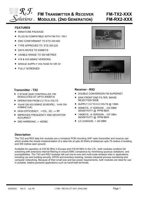
Transmitter - <strong>TX2</strong><br />
• 2 STAGE SAW CONTROLLED, <strong>FM</strong><br />
MODULATED AT UPTO 40KBIT/S<br />
• OPERATION FROM 2.2 TO 6 VOLTS<br />
• 10mW ON 433.92MHZ (EUROPE) , 1mW ON<br />
418MHZ (UK)<br />
• HIGH EFFICIENCY, >15% , DC --> RF<br />
• IMPROVED FREQUENCY AND DEVIATION<br />
ACCURACY<br />
• 2ND HARMONIC, < -60DBC<br />
Description<br />
Receiver - <strong>RX2</strong><br />
• DOUBLE CONVERSION <strong>FM</strong> SUPERHET<br />
• SAW FRONT END FILTER, IMAGE<br />
REJECTION 50DB<br />
• SUPPLY 3.0 TO 6.0 VOLTS @ 13MA<br />
• 40KBIT/S, -F VERSION , -100 DBM<br />
SENSITIVITY @ 1PPM BER<br />
• 14KBIT/S. -A VERSION , -107 DBm<br />
SENSITIVITY @ 1PPM BER<br />
• LO LEAKAGE, < -60 DBM<br />
The <strong>TX2</strong> and <strong>RX2</strong> data link modules are a miniature PCB mounting UHF radio transmitter and receiver pair<br />
which enable the simple implementation of a data link at upto 40 Kbit/s at distances upto 75 metres in-building<br />
and 300 metres open ground.<br />
Available for operation at 433.92 MHz in Europe and 418.00 MHz in the U.K., both modules combine full<br />
screening with extensive internal filtering to ensure EMC compliance by minimising spurious radiations and<br />
susceptibilities. The <strong>TX2</strong> and <strong>RX2</strong> modules will suit one-to-one and multi-node wireless links in applications<br />
including car and building security, EPOS and inventory tracking, remote industrial process monitoring and<br />
computer networking. Because of their small size and low power requirements, both modules are ideal for use<br />
in portable, battery-powered applications such as hand-held terminals.<br />
DS000022 Rev D July ‘99 ©1999 REG No 277 4001, ENGLAND. Page 1
<strong>FM</strong> TRANSMITTER & RECEIVER <strong>FM</strong>-<strong>TX2</strong>-<strong>XXX</strong><br />
MODULES. (2ND GENERATION) <strong>FM</strong>-<strong>RX2</strong>-<strong>XXX</strong><br />
Functional description:<br />
The <strong>TX2</strong> transmitter module is a two stage, SAW controlled <strong>FM</strong> transmitter operating between<br />
2V and 6V and is available in 433.92MHz and 418.00 MHz versions. The 433.92 MHz unit is<br />
type-approved to ETS 300-220 for European use and delivers nominally +9dBm from a 5V<br />
supply at 12mA, while the 418.00 MHz unit has MPT 1340 type-approval for U.K. use and<br />
delivers -3dBm from a 5V supply at 5mA. Both modules measure 12 x 32 x 3.8 mm.<br />
The <strong>RX2</strong> module is a double conversion <strong>FM</strong> superhet receiver capable of handling date rates of<br />
upto 40kbit/s. The SIL style <strong>RX2</strong> receiver measures 17.5 x 48 x 4.5 mm. It will operate from a<br />
supply of 3-6V and draws 14mA when receiving. A fast-acting carrier detect and a power-up<br />
enable time of less than 1ms This allows effective duty cycle power saving and a -107 dBm<br />
sensitivity. This, combined with a SAW front-end filter results in an excellent RF performance<br />
and EMC conformance.<br />
<strong>TX2</strong> transmitter:<br />
Pin description:<br />
RF GND (pin 1)<br />
RF ground pin, internally connected to<br />
the module screen and pin 4 (0V). This<br />
pin should be connected to the RF<br />
return path (e.g. coax braid, main PCB<br />
ground plane etc.)<br />
RF out (pin 2)<br />
50Ω RF output to the antenna, it is DC<br />
isolated internally. (see antenna section<br />
of <strong>TX2</strong> applications note for suggested<br />
antenna/feeds).<br />
fig. 1: <strong>TX2</strong> block diagram<br />
Vcc (pin 3)<br />
+ve supply pin. The module will generate RF when the Vcc supply is present. Max ripple<br />
content 0.1VP-P. A 100nF de-coupling ceramic capacitor is suggested.<br />
0V (pin 4)<br />
Supply ground connection, connected to pin 1 and screen.<br />
TXD (pin 5)<br />
This DC coupled modulation input will accept either serial digital data ( 0V to Vcc levels) or<br />
high level linear signals. see <strong>TX2</strong> applications note for suggested drive methods. Input<br />
impedance is 100kΩ.<br />
DS000022 Rev D July ‘99 ©1999 REG No 277 4001, ENGLAND. Page 2
<strong>RX2</strong> receiver:<br />
Pin description<br />
<strong>FM</strong> TRANSMITTER & RECEIVER <strong>FM</strong>-<strong>TX2</strong>-<strong>XXX</strong><br />
MODULES. (2ND GENERATION) <strong>FM</strong>-<strong>RX2</strong>-<strong>XXX</strong><br />
RF in (pin 1)<br />
50Ω RF input from the antenna,<br />
it is DC isolate internally. (see<br />
antenna section of <strong>RX2</strong><br />
applications note for suggested<br />
antenna/feeds).<br />
RF GND (pin 2)<br />
RF ground pin, internally<br />
connected to the module screen<br />
and pin 4 (0V). This pin should<br />
be connected to the RF return<br />
path (e.g. coax braid, main PCB<br />
ground plane etc.)<br />
CD (pin 3)<br />
The Carrier Detect may be used to drive an external PNP transistor to obtain a logic<br />
level carrier detect signal, see test circuit / applications note. If not required it should<br />
be connected to pin 5 (Vcc).<br />
0volt (pin 4)<br />
Supply ground connection, connected to pin 1 and screen.<br />
fig. 3: <strong>RX2</strong> block diagram<br />
fig. 4: physical dimensions<br />
Vcc (pin 5)<br />
+ve supply pin. +3.0V to +6.0V @ 2kΩ and < 100pF.<br />
RXD (pin 7)<br />
This digital output from the internal data slicer is a squared version of the signal on<br />
pin 6 (AF). It may be used to drive external decoders. The data is true data, i.e. as fed<br />
to the transmitter. Load impedance should be > 1kΩ and < 1nF<br />
DS000022 Rev D July ‘99 ©1999 REG No 277 4001, ENGLAND. Page 3
<strong>FM</strong> TRANSMITTER & RECEIVER <strong>FM</strong>-<strong>TX2</strong>-<strong>XXX</strong><br />
MODULES. (2ND GENERATION) <strong>FM</strong>-<strong>RX2</strong>-<strong>XXX</strong><br />
Absolute Maximums:<br />
Operating temperature: -10°C to +55°C Storage temperature : -40°C to +100°C<br />
<strong>TX2</strong>, all variants<br />
Vcc (pin 3) -0.1V to +10.0V<br />
Data input (pin 5) -0.1V to +10.0V<br />
RF out (pin 2) ±50V @ < 10MHz , +20dBm @ > 10MHz<br />
<strong>RX2</strong>, all variants<br />
Vcc (pin 5) -0.1V to +10.0V<br />
Data , CD & AF (pin 7,3,6) -0.1V to + Vcc V<br />
RF input (pin 1) ±50V @ < 10MHz , +13dBm @ > 10MHz<br />
note: Operation of the <strong>TX2</strong> above 6V may cause the module to exceed the licensed<br />
power level.<br />
Electrical Performance: <strong>TX2</strong> transmitter<br />
pin min. typ. max. units notes<br />
DC LEVELS<br />
supply voltage 3 2.2 3.0 4.0 V -3V version<br />
supply voltage 3 4.0 5.0 6.0 V -5V version<br />
CURRENT & RF POWER<br />
<strong>TX2</strong>-418-3V<br />
supply current @ Vcc = 3V 3 4 6 10 mA<br />
RF power @ Vcc = 3V 2 -7 -3 +3 dBm 1<br />
<strong>TX2</strong>-418-5V<br />
supply current @ Vcc = 5V 3 4 6 10 mA<br />
RF power @ Vcc = 5V 2 -7 -3 +3 dBm 1<br />
<strong>TX2</strong>-433-3V<br />
supply current @ Vcc = 3V 3 4 6 10 mA<br />
RF power @ Vcc = 3V 2 0 +4 +6 dBm 1<br />
<strong>TX2</strong>-433-5V<br />
supply current @ Vcc = 5V 3 7 10 14 mA<br />
RF power @ Vcc = 5V 2 +6 +9 +12 dBm 1<br />
RF<br />
2 nd harmonic 2 - -65 -54 dBc 1<br />
Harmonics @ > 1GHz 2 - -50 -40 dBc 1<br />
initial frequency accuracy - -30 0 +30 kHz<br />
overall frequency accuracy - -70 - +70 kHz<br />
<strong>FM</strong> deviation (+/-) - 20 25 30 kHz<br />
Modulation bandwidth @ -3dB - DC - 20 kHz<br />
Modulation distortion (THD) - - 5 10 %<br />
power up time to full RF - - - 100 μs<br />
note: 1. Measured into a 50Ω load.<br />
DS000022 Rev D July ‘99 ©1999 REG No 277 4001, ENGLAND. Page 4
<strong>FM</strong> TRANSMITTER & RECEIVER <strong>FM</strong>-<strong>TX2</strong>-<strong>XXX</strong><br />
MODULES. (2ND GENERATION) <strong>FM</strong>-<strong>RX2</strong>-<strong>XXX</strong><br />
Electrical Performance: <strong>RX2</strong> Receiver<br />
Figures apply to 5V versions unless noted otherwise Vcc = 5.0V, temperature 20°C unless noted otherwise<br />
pin min. typ. Max. units notes<br />
DC LEVELS<br />
supply voltage, Vcc standard 5 4.0 5.0 6.0 V<br />
supply voltage, Vcc, 3V version 5 3.0 3.5 4.0 V<br />
supply current 5 11 13 17 mA<br />
supply ripple 5 - - 2 mVP-P 1<br />
data output high, 100μA source 7 - Vcc-0.6 - V<br />
data output low, 100μA sink 7 - 0.4 - V<br />
load capacitance on AF / Data 6,7 - - 100 pF<br />
RF<br />
RF sensitivity for 10dB (S+N)/N 1,6 - -113 -107 dBm -A version<br />
RF sensitivity for 10dB (S+N)/N 1,6 - -107 -100 dBm -F version<br />
RF sensitivity for 1ppm BER 1,6 - -107 -100 dBm -A version<br />
RF sensitivity for 1ppm BER 1,6 - -100 -93 dBm -F version<br />
CD threshold 1,3 - -107 -97 dBm -A version<br />
CD threshold 1,3 - 100 -90 dBm -F version<br />
IF band width - - 250 - kHz<br />
initial frequency accuracy 1 -30 0 +30 kHz<br />
E.M.C.<br />
image rejection (2*FIF) 1 - -50 - dB 2<br />
spurious responses upto 1GHz 1 - -70 - dB 2<br />
LO leakage, conducted 1 - -65 - dBm<br />
LO leakage, radiated - - -70 - dBm<br />
AF BASE BAND<br />
baseband bandwidth @ -3dB 6 0.006 - 7 kHz -A version<br />
baseband bandwidth @ -3dB 6 0.060 - 20 kHz -F version<br />
AF level 6 - 450 - mVP-P<br />
DC offset on AF 6 0.8 1.2 1.6 V<br />
distortion on recovered AF 6 - 0.5 1 %<br />
ultimate (S+N)/N 6 35 45 - dB<br />
DYNAMIC TIMING<br />
Power up with signal present<br />
power up to valid CD, TPU-CD - - 1 - ms<br />
power up to stable data, TPU-DAT - - 20 - ms -A version<br />
power up to stable data, TPU-DAT - - 5 - ms -F version<br />
Signal applied with supply on<br />
signal to valid CD, TSIG-CD - - 0.5 - ms<br />
signal to stable data, TSIG-DAT - - 15 - ms<br />
signal to stable data, TSIG-DAT - - 3 - ms<br />
time between data transitions 7 15 - 0.07 ms 4,-A version<br />
time between data transitions 7 1.5 - 0.025 ms 4,-F version<br />
mark:space ratio - 20 50 80 % 3<br />
notes: 1. For 6dB (S+N)/N degradation on wanted -100dBm signal<br />
2. Receiver spurious responses are at FRF ± (n×15.92MHz), n=1,2,3 etc.<br />
3. Average over 30ms (-A), 3ms (-F) at maximum bit rate.<br />
4. Values for 50:50 mark to space (i.e. square wave)<br />
DS000022 Rev D July ‘99 ©1999 REG No 277 4001, ENGLAND. Page 5
Module test circuits<br />
<strong>FM</strong> TRANSMITTER & RECEIVER <strong>FM</strong>-<strong>TX2</strong>-<strong>XXX</strong><br />
MODULES. (2ND GENERATION) <strong>FM</strong>-<strong>RX2</strong>-<strong>XXX</strong><br />
fig.5: <strong>TX2</strong> test circuit<br />
fig.6: <strong>RX2</strong> test circuit<br />
∗ The PNP transistor enables a CMOS compatible Carrier Detect signal to be derived from pin 3. If no CD signal required<br />
pin 3 should be connected directly to pin 5 (Vcc)<br />
Module mounting considerations<br />
The modules may be mounted horizontally or vertically on an area of ground plane preferably<br />
close to the antenna to minimise feed length. The receiver and it’s antenna should be kept away<br />
from sources of interference (micro’s, SMPS etc.). The modules may be potted if required in a<br />
viscous compound which can not enter the screen can..<br />
Warning: Do NOT wash the modules. They are not hermetically sealed.<br />
DS000022 Rev D July ‘99 ©1999 REG No 277 4001, ENGLAND. Page 6
Antenna requirements<br />
<strong>FM</strong> TRANSMITTER & RECEIVER <strong>FM</strong>-<strong>TX2</strong>-<strong>XXX</strong><br />
MODULES. (2ND GENERATION) <strong>FM</strong>-<strong>RX2</strong>-<strong>XXX</strong><br />
Three types of integral antenna are recommended and approved for use with the module:<br />
Helical Wire coil, connected directly to pin 2, open circuit at other end. This antenna is<br />
very efficient given it's small size (20mm x 4mm dia.). The helical is a high Q<br />
antenna, trim the wire length or expand the coil for optimum results. The helical<br />
de-tunes badly with proximity to other conductive objects.<br />
Loop A loop of PCB track tuned by a fixed or variable capacitor to ground at the 'hot'<br />
end and fed from pin 2 at a point 20% from the ground end. Loops have high<br />
immunity to proximity de-tuning.<br />
Whip This is a wire, rod, PCB track or combination connected directly to pin 2<br />
of the module. Optimum total length is 17cm (1/4 wave @ 418MHz) Keep<br />
the open circuit (hot) end well away from metal components to prevent<br />
serious de-tuning. Whips are ground plane sensitive and will benefit from<br />
internal 1/4 wave earthed radial(s) if the product is small and plastic<br />
cased<br />
helical loop whip<br />
Ultimate performance ** * ***<br />
Easy of design set-up ** * ***<br />
Size *** ** *<br />
Immunity proximity effects ** *** *<br />
Range open ground to similar antenna<br />
(for <strong>TX2</strong>-433-A & <strong>RX2</strong>-433-A)<br />
200m 100m 300m<br />
The antenna choice and position directly controls the system range. Keep it clear of other metal<br />
in the system, particularly the 'hot' end. The best position by far, is sticking out the top of the<br />
product. This is often not desirable for practical/ergonomic reasons thus a compromise may need<br />
to be reached. If an internal antenna must be used try to keep it away from other metal<br />
components, particularly large ones like transformers, batteries and PCB tracks/earth plane. The<br />
space around the antenna is as important as the antenna itself.<br />
Antenna selection chart<br />
Fig.8: antenna configurations<br />
DS000022 Rev D July ‘99 ©1999 REG No 277 4001, ENGLAND. Page 7
<strong>FM</strong> TRANSMITTER & RECEIVER <strong>FM</strong>-<strong>TX2</strong>-<strong>XXX</strong><br />
MODULES. (2ND GENERATION) <strong>FM</strong>-<strong>RX2</strong>-<strong>XXX</strong><br />
Type Approval in UK<br />
The <strong>TX2</strong>-418 is type approved in the UK to MPT1340 for use in Telemetry, Telecommand and In-<br />
Building alarm applications.<br />
CONFORMANCE to MPT1340 REQUIRES THAT:<br />
1. The transmitting antenna must be one of the 3 variants given in the data sheet. Antenna<br />
structures which yield ERP gain are not permitted.<br />
2. The module must be directly and permanently connected to the transmitting antenna without<br />
the use of an external feeder. Increasing the RF power level by any means is not permitted.<br />
3. The module must not be modified nor used outside it's specification limits.<br />
4. The module may only be used to send digital or digitised data. Speech and/or music are not<br />
permitted.<br />
5. The equipment in which the module is used must carry an inspection mark located on the<br />
outside of the equipment and be clearly visible. The minimum dimensions of the inspection<br />
mark shall be 10 x 15 mm and the letter and figure height must be no less than 2mm. The<br />
wording shall read:<br />
RTD: xxxxxx<br />
SRD-MPT1340-GB<br />
6. Products intended for UK commercial application must be notified to the<br />
Radiocommunications Agency (RA) on form RA 249 ( Cat I), obtainable from the RA's library<br />
service, Tel 0171 211 0502 / 0505<br />
OEM Manufacturers incorporating the <strong>TX2</strong> as a component part of their product are authorised<br />
by Radiometrix Ltd to quote their type-approval provided all the above conditions are complied<br />
with.<br />
European type approval<br />
The <strong>TX2</strong>-433 & <strong>RX2</strong>-433 are type approved to ETS 300-220 for European use.<br />
CONFORMANCE to ETS 300-220 REQUIRES THAT:<br />
1. The transmitting antenna must be one of the 3 variants given in the data sheet. Antenna<br />
structures which yield ERP gain are not permitted.<br />
2. The module must be directly and permanently connected to the transmitting antenna without<br />
the use of an external feeder. Increasing the RF power level by any means is not permitted.<br />
3. The module must not be modified nor used outside it's specification limits.<br />
4. The equipment in which the module is used must carry an inspection mark located on the<br />
outside of the equipment and be clearly visible. The minimum dimensions of the inspection<br />
mark shall be 10 x 15 mm and the letter and figure height must be no less than 2mm. The<br />
wording shall read:<br />
Radiometrix<br />
<strong>TX2</strong>-433<br />
CEPT-LPD-xx<br />
respectively,<br />
Radiometrix<br />
<strong>RX2</strong>-433<br />
CEPT-LPD-xx<br />
OEM Manufacturers incorporating the <strong>TX2</strong> & <strong>RX2</strong> as a component part of their product are<br />
authorised by Radiometrix Ltd to quote our type-approval provided all the above conditions are<br />
complied with.<br />
Most EEC member countries require notification before your product may be sold. We advise<br />
you to contact the relevant country.<br />
DS000022 Rev D July ‘99 ©1999 REG No 277 4001, ENGLAND. Page 8
<strong>FM</strong> TRANSMITTER & RECEIVER <strong>FM</strong>-<strong>TX2</strong>-<strong>XXX</strong><br />
MODULES. (2ND GENERATION) <strong>FM</strong>-<strong>RX2</strong>-<strong>XXX</strong><br />
Variants and Ordering information<br />
The <strong>TX2</strong> transmitter and <strong>RX2</strong> receiver are manufactured in several variants<br />
Frequencies 418.00 MHz for UK use<br />
433.92 MHz for European use<br />
Supply voltage 5V ( 4V to 6V <strong>TX2</strong> & <strong>RX2</strong>)<br />
3V ( 3V to 4V for <strong>RX2</strong>, 2.2V to 4V for <strong>TX2</strong>)<br />
RX data rate: -A, 7kHz baseband BW, slow data upto 14kbps<br />
-F, 20kHz baseband BW, fast data upto 40kbps<br />
RX data rate applies to receivers only, the <strong>TX2</strong> will handle fast or slow data.<br />
PART No DESCRIPTION<br />
<strong>FM</strong>-<strong>TX2</strong>-418-5V Transmitter 418MHz 5 Volt Operation -6dBm<br />
<strong>FM</strong>-<strong>TX2</strong>-418-3V Transmitter 418MHz 3 Volt Operation -6dBm<br />
<strong>FM</strong>-<strong>TX2</strong>-433-5V Transmitter 433MHz 5 Volt Operation +9dBm<br />
<strong>FM</strong>-<strong>TX2</strong>-433-3V Transmitter 433MHz 3 Volt Operation +9dBm<br />
<strong>FM</strong>-<strong>RX2</strong>-418A-5V Receiver, 418MHz 5 Volt Operation 14kbps<br />
<strong>FM</strong>-<strong>RX2</strong>-418F-5V Receiver, 418MHz 5 Volt Operation. Fast Version 40kbps<br />
<strong>FM</strong>-<strong>RX2</strong>-433A-5V Receiver, 433MHz 5 Volt Operation 14kbps<br />
<strong>FM</strong>-<strong>RX2</strong>-433F-5V Receiver, 433MHz 5 Volt Operation. Fast Version 40kbps<br />
<strong>FM</strong>-<strong>RX2</strong>-418A-3V Receiver, 418MHz 3 Volt Operation 14kbps<br />
<strong>FM</strong>-<strong>RX2</strong>-418F-3V Receiver, 418MHz 3 Volt Operation. Fast Version 40kbps<br />
<strong>FM</strong>-<strong>RX2</strong>-433A-3V Receiver, 433MHz 3 Volt Operation 14kbps<br />
<strong>FM</strong>-<strong>RX2</strong>-433F-3V Receiver, 433MHz 3 Volt Operation. Fast Version 40kbps<br />
Should you require further assistance, please call;<br />
R. F. Solutions Ltd.,<br />
Unit 21, Cliffe Industrial Estate,<br />
South Street,<br />
Lewes,<br />
E Sussex, BN8 6JL. England.<br />
Tel +44 (0)1273 898 000. Fax +44 (0)1273 480 661.<br />
Email sales@rfsolutions.co.uk http://www.rfsolutions.co.uk<br />
RF Solutions is a member of the Low Power Radio Association.<br />
RF module data appears courtesy of Radiometrix Ltd, Middlesex, England.<br />
Limitation of Liability<br />
The information furnished by RF Solutions Ltd. is believed to be accurate and reliable. RF Solutions Ltd reserves the right to make changes or improvements in the design,<br />
specification or manufacture of its sub-assembly products without notice. RF Solutions Ltd does not assume any liability arising from the application or use of any product<br />
or circuit described herein, nor for any infringements of patents or other rights of third parties which may result from the use of its products. This data sheet neither states<br />
nor implies warranty of any kind, including fitness for any particular application. These radio devices may be subject to radio interference and may not function as intended<br />
if interference is present. We do NOT recommend their use for life critical applications.<br />
Radio and EMC Regulations<br />
The Intrastat commodity code for all our modules is : 8542 4090. The purchaser of RF Solutions Ltd sub-assemblies must satisfy all relevant EMC and Radio regulations<br />
which applies to the finished products in the country of use.<br />
Information contained in this document is believed to be accurate , however no representation or warranty is given and no liability is assumed by R.F. Solutions Ltd. with respect to the accuracy of<br />
such information. Use of R.F.Solutions as critical components in life support systems is not authorised except with express written approval from R.F.Solutions Ltd.<br />
DS000022 Rev D July ‘99 ©1999 REG No 277 4001, ENGLAND. Page 9