VIII.2. A Semiconductor Device Primer
VIII.2. A Semiconductor Device Primer
VIII.2. A Semiconductor Device Primer

You also want an ePaper? Increase the reach of your titles
YUMPU automatically turns print PDFs into web optimized ePapers that Google loves.
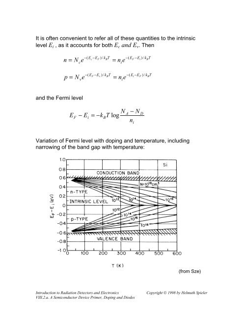
It is often convenient to refer all of these quantities to the intrinsic<br />
level Ei , as it accounts for both Ec and Ev. Then<br />
n =<br />
p =<br />
N<br />
N<br />
and the Fermi level<br />
E<br />
F<br />
c<br />
v<br />
e<br />
e<br />
−(<br />
Ec−<br />
EF<br />
) / kBT<br />
−(<br />
EF<br />
−Ei<br />
) / k<br />
= nie<br />
−(<br />
EF<br />
−Ev<br />
) / kBT<br />
−(<br />
Ei<br />
−E<br />
= nie<br />
N<br />
− E = −k<br />
T log<br />
i<br />
B<br />
Variation of Fermi level with doping and temperature, including<br />
narrowing of the band gap with temperature:<br />
(from Sze)<br />
Introduction to Radiation Detectors and Electronics Copyright © 1998 by Helmuth Spieler<br />
<strong>VIII.2.</strong>a. A <strong>Semiconductor</strong> <strong>Device</strong> <strong>Primer</strong>, Doping and Diodes<br />
A<br />
i<br />
F<br />
− N<br />
n<br />
B<br />
) / k<br />
D<br />
B<br />
T<br />
T