75W SMPS with TEA1507 Quasi- Resonant Flyback controller - NXP ...
75W SMPS with TEA1507 Quasi- Resonant Flyback controller - NXP ...
75W SMPS with TEA1507 Quasi- Resonant Flyback controller - NXP ...
Create successful ePaper yourself
Turn your PDF publications into a flip-book with our unique Google optimized e-Paper software.
Philips Semiconductors<br />
Application Note<br />
AN00047<br />
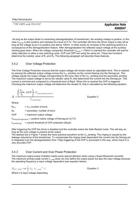
As long as the output diode is conducting (demagnetization of transformer), the winding voltage is positive. In this<br />
case Vdemag is also positive and clamped at a level of 0.7V. The <strong>controller</strong> will force the driver output to stay off as<br />
long as the voltage at pin 4 is positive and above 100mV. In other words an increase of the switching period is a<br />
consequence of the demagnetization feature. After demagnetization the reflected output voltage at the auxiliary<br />
winding goes down. When the voltage comparator threshold Vdemag < 100mV is reached the <strong>controller</strong> will wait for<br />
valley detection to allow a new switching cycle. OVP and OPP are using the same pin. These two functions<br />
determine the resistor value of R1 and R2. The following paragraph will describe these features.<br />
3.4.2 Over Voltage Protection<br />
The Over Voltage Protection ensures that the output voltage will remain below an adjustable level. This is realized<br />
by sensing the reflected output voltage across the VCC winding via the current flowing into the Demag pin. This<br />
voltage equals the output voltage corresponding to the turns ratio of the VCC winding and the secondary winding.<br />
The maximum output voltage is set by the resistor value R1 that determines the current into the Demag pin. This<br />
current is mirrored and compared to a threshold level of 60μA. When this is reached the OVP is triggered.<br />
Choosing the maximum output voltage will determine the resistor R1 that is calculated by the following equation:<br />
R<br />
⎛ N<br />
⎜<br />
⎞<br />
⋅OVP⎟<br />
−V<br />
Vcc<br />
⎜<br />
clamp,<br />
demag ( positive)<br />
N ⎟<br />
s<br />
1 =<br />
⎝ ⎠<br />
Equation 2<br />
I ( ovp)(<br />
demag)<br />
Where,<br />
NVcc = VCC number of turns<br />
NS = secondary number of turns<br />
OVP = maximum output voltage<br />
Vclamp,Demag(positive) = positive clamp voltage of Demag pin (0.7V)<br />
I(ovp)(Demag) = current threshold of OVP protection (60μA)<br />
After triggering the OVP the driver is disabled and the <strong>controller</strong> enters the Safe-Restart mode. This will stay as<br />
long as the over voltage is present at the output.<br />
The dashed line in Figure 7 shows the more practical waveform at the Vcc winding. The ringing is caused by the<br />
leakage inductance of the transformer. To compensate this ringing (load dependent) the current into the Demag pin<br />
is integrated over the demagnetization time. False triggering of the OVP is prevented in this way, which result in a<br />
very accurate OVP.<br />
3.4.3 Over Current and Over Power Protection<br />
The maximum output power limitation needs some special attention when using a <strong>Quasi</strong>-<strong>Resonant</strong> converter.<br />
The maximum primary peak current IL_peak does not only define the output power but also the input voltage because<br />
the operating frequency is input voltage dependent (see equation below).<br />
1<br />
2<br />
POUT _ MAX = η ⋅ ⋅ LP<br />
⋅ I L _ peak ⋅ f Equation 3<br />
2<br />
Where f is input voltage depending<br />
14


