75W SMPS with TEA1507 Quasi- Resonant Flyback controller - NXP ...
75W SMPS with TEA1507 Quasi- Resonant Flyback controller - NXP ...
75W SMPS with TEA1507 Quasi- Resonant Flyback controller - NXP ...
Create successful ePaper yourself
Turn your PDF publications into a flip-book with our unique Google optimized e-Paper software.
Philips Semiconductors<br />
Application Note<br />
AN00047<br />
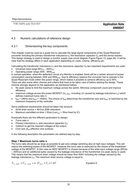
4.3 Numeric calculations of reference design<br />
4.3.1 Dimensioning the key components<br />
This chapter could be used as a guide line to calculate the large signal components of the <strong>Quasi</strong>-<strong>Resonant</strong><br />
converter including the primary transformer inductance LP the resonance capacitor CD and the sense resistor.<br />
This design strategy is used to design a monitor supply (see circuit diagram Figure Figure 12, page 26). It will be<br />
clear that the strategy differs in each application depending on costs, volume, efficiency etc.<br />
Calculating the transformer inductance LP and the resonance capacitor CD two important requirements are used:<br />
• Universal input range 85VAC…264VAC;<br />
• Operating power range 20W…85Wpeak.<br />
In normal operation, when the deflection circuit of a Monitor is enabled, there will be a certain amount of power<br />
consumption varying between 20W and 85Wpeak. Due to efficiency reasons the converter has to operate in the<br />
<strong>Quasi</strong>-<strong>Resonant</strong> mode <strong>with</strong>in this power range, which makes it possible to achieve efficiency up to 90%.<br />
There are also some other choices and criteria that have to be taken care of before starting the design. These<br />
choices strongly depend on the application as mentioned before.<br />
• No peak clamp to limit the maximum voltage across the switch. Minimize component count and improve<br />
efficiency;<br />
• maximum voltage across the power MOSFET (VD_MAX, including ΔV caused by leakage inductance Ls) which<br />
defines maximum turns ratio n;<br />
• fMIN = 25kHz and fMAX = 150kHz. The choice of fMIN determines the transformer size and fMAX is restricted by the<br />
maximum frequency of the <strong>controller</strong>.<br />
Some additional requirements should be taken into account:<br />
• dV/dt drain source < 4kV/us (EMI reduction)<br />
• Maximum permitted on-time < 50us (t-onmax = 50us fixed by IC)<br />
Eventually there are five different parameters to design:<br />
• Turns ratio n;<br />
• Primary inductance LP and resonance capacitor CD;<br />
• Volt/turn to get the required voltages at the output;<br />
• Core size (Aeff effective core surface).<br />
In the following description the parameters are defined step by step.<br />
Step 1 Maximum turns ratio n<br />
The turns ratio should be as large as possible to get zero voltage switching also at high input voltages. This will<br />
reduce the switching losses of the MOSFET. However the turns ratio is restricted by the choice of the breakdown<br />
voltage of the MOSFET. In this case an 800V MOSFET is chosen because of the wide input voltage range (85Vac<br />
– 264Vac) and an additional spike caused by the leakage inductance of the transformer (no peak clamp is used).<br />
This means that the maximum drain voltage should be lower than 800V including the voltage caused by the<br />
leakage inductance LS. The maximum drain source voltage is equal to:<br />
VD _ MAX IN _ MAX<br />
OUT F<br />
= V + n ⋅ ( V + V ) + ΔV<br />
20<br />
Equation 6


