Chapter 8 Summary: The 8086 Microprocessor and its Memory and ...
Chapter 8 Summary: The 8086 Microprocessor and its Memory and ...
Chapter 8 Summary: The 8086 Microprocessor and its Memory and ...

Create successful ePaper yourself
Turn your PDF publications into a flip-book with our unique Google optimized e-Paper software.
<strong>Chapter</strong> 8 <strong>Summary</strong>: <strong>The</strong> <strong>8086</strong><br />
<strong>Microprocessor</strong> <strong>and</strong> <strong>its</strong> <strong>Memory</strong> <strong>and</strong><br />
Input/Output Interface<br />
Figure 1-5 Intel Corporation’s <strong>8086</strong> <strong>Microprocessor</strong>.<br />
• <strong>The</strong> <strong>8086</strong>, announced in 1978, was the first 16-bit microprocessor introduced by<br />
Intel Corporation.<br />
• <strong>The</strong> <strong>8086</strong> is internally a 16-bit MPU <strong>and</strong> externally it has a 16-bit data bus. It<br />
has the ability to address up to 1 Mbyte of memory via <strong>its</strong> 20-bit address bus.<br />
• In addition, it can address up to 64K of byte-wide input/output ports.<br />
• It is manufactured using high-performance metal-oxide semiconductor<br />
(HMOS) technology, <strong>and</strong> the circuitry on <strong>its</strong> chip is equivalent to approximately<br />
29,000 transistors.<br />
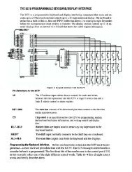
• <strong>The</strong> <strong>8086</strong> is housed in a 40-pin dual in-line package. <strong>The</strong> signals pinned out to<br />
each lead are shown in Fig. 8-1.<br />
• <strong>The</strong> address bus lines A0 through A15 <strong>and</strong> data bus lines D0 through D15 are<br />
multiplexed. For this reason, these leads are labeled AD0 through AD15. By<br />
multiplexed we mean that the same physical pin carries an address bit at one time<br />
<strong>and</strong> the data bit at another time.<br />
1
Figure 8-1 Pin layout of the <strong>8086</strong> <strong>Microprocessor</strong>.<br />
2
8.2 MINIMUM-MODE AND MAXIMUM-MODE<br />
• <strong>The</strong> <strong>8086</strong> can be configured to work in either of two modes:<br />
• <strong>The</strong> minimum mode is selected by applying logic 1 to the MN/ MX input lead. It<br />
is typically used for smaller single microprocessor systems.<br />
• <strong>The</strong> maximum mode is selected by applying logic 0 to the MN/ MX input lead.<br />
It is typically used for larger multiple microprocessor systems.<br />
• Depending on the mode of operation selected, the assignments for a number of<br />
the pins on the microprocessor package are changed. <strong>The</strong> pin functions<br />
specified in parentheses pertain to the maximum-mode.<br />
• We will only discuss minimum-mode operation of the <strong>8086</strong>. In minimum<br />
mode, the <strong>8086</strong> <strong>its</strong>elf provides all the control signals needed to implement the<br />
memory <strong>and</strong> I/O interfaces (see Fig. 8-3). In maximum-mode, a separate chip<br />
(the 8288 Bus Controller) is used to help in sending control signals over the<br />
shared bus (see Fig. 8-5).<br />
3
8.3 SUMMARY OF MINIMUM-MODE INTERFACE SIGNALS<br />
• Address/Data Bus: <strong>The</strong> address bus is 20 b<strong>its</strong> long <strong>and</strong> consists of signal lines<br />
A0 (LSB) through A19 (MSB). However, only address lines A0 through A15 are<br />
used when accessing I/O.<br />
• <strong>The</strong> data bus lines are multiplexed with address lines. For this reason, they are<br />
denoted as AD0 through AD15. Data line D0 is the LSB.<br />
• Status Signals: <strong>The</strong> four most significant address lines A16 through A19 of the<br />
<strong>8086</strong> are multiplexed with status signals S3 through S6. <strong>The</strong>se status b<strong>its</strong> are<br />
output on the bus at the same time that data are transferred over the other bus<br />
lines.<br />
4
• Control Signals:<br />
• When Address latch enable (ALE) is logic 1 it signals that a valid address is on<br />
the bus. This address can be latched in external circuitry on the 1-to-0 edge of<br />
the pulse at ALE.<br />
• M/ IO (memory/IO) tells external circuitry whether a memory or I/O transfer is<br />
taking place over the bus. Logic 1 signals a memory operation <strong>and</strong> logic 0<br />
signals an I/O operation.<br />
• DT/ R (data transmit/receive) signals the direction of data transfer over the<br />
bus. Logic 1 indicates that the bus is in the transmit mode (i.e., data are either<br />
written into memory or to an I/O device). Logic 0 signals that the bus is in the<br />
receive mode (i.e., reading data from memory or from an input port).<br />
• <strong>The</strong> bank high enable (BHE ) signal is used as a memory enable signal for the<br />
most significant byte half of the data bus, D8 through D15.<br />
• WR (write) is switched to logic 0 to signal external devices that valid output<br />
data are on the bus.<br />
• RD (read) indicates that the MPU is performing a read of data off the bus.<br />
During read operations, one other control signal, DEN (data enable), is also<br />
supplied. It enables external devices to supply data to the microprocessor.<br />
• <strong>The</strong> READY signal can be used to insert wait states into the bus cycle so that it<br />
is extended by a number of clock periods. This signal is supplied by a slow<br />
memory or I/O subsystem to signal the MPU when it is ready to permit the<br />
data transfer to be completed.<br />
• Interrupt Signals:<br />
• Interrupt request (INTR) is an input to the <strong>8086</strong> that can be used by an external<br />
device to signal that it needs to be serviced. Logic 1 at INTR represents an<br />
active interrupt request.<br />
• When the MPU recognizes an interrupt request, it indicates this fact to<br />
external circu<strong>its</strong> with logic 0 at the interrupt acknowledge (INTA) output.<br />
• On the 0-to-1 transition of nonmaskable interrupt (NMI), control is passed to a<br />
nonmaskable interrupt service routine at completion of execution of the<br />
current instruction. NMI is the interrupt request with highest priority <strong>and</strong> cannot<br />
be masked by software.<br />
5
• <strong>The</strong> RESET input is used to provide a hardware reset for the MPU. Switching<br />
RESET to logic 0 initializes the internal registers of the MPU <strong>and</strong> initiates a<br />
reset service routine.<br />
• DMA Interface Signals:<br />
• When an external device wants to take control of the system bus, it signals this<br />
fact to the MPU by switching HOLD to the logic level 1.<br />
• When in the hold state, lines AD0 through AD15, A16/S3 through A19/S6, BHE ,<br />
M/ IO,<br />
DT/ R , WR , RD , DEN <strong>and</strong> INTR are all put in the high-Z state. <strong>The</strong><br />
MPU signals external devices that it is in this state by switching HLDA to 1.<br />
8.6 SYSTEM CLOCK<br />
• To synchronize the internal <strong>and</strong> external operations of the microprocessor a<br />
clock (CLK) input signal is used. <strong>The</strong> CLK can be generated by the 8284 clock<br />
generator IC.<br />
• <strong>The</strong> <strong>8086</strong> is manufactured in three speeds: 5 MHz, 8 MHz <strong>and</strong> 10 MHz.<br />
• For <strong>8086</strong>, we connect either a 15-, 24- or 30-MHz crystal between inputs X1<br />
<strong>and</strong> X2 inputs of the clock chip (see Fig. 8-11). <strong>The</strong> fundamental crystal<br />
frequency is divided by 3 within the 8284 to give either a 5-, 8- or 10-MHz<br />
clock signal, which is directly connected to the CLK input of the <strong>8086</strong>.<br />
8.7 BUS CYCLE AND TIME STATES<br />
• A bus cycle defines the sequence of events when the MPU communicates with<br />
an external device, which starts with an address being output on the system bus<br />
followed by a read or write data transfer.<br />
6
• Types of bus cycles:<br />
o <strong>Memory</strong> Read Bus Cycle<br />
o <strong>Memory</strong> Write Bus Cycle<br />
o Input/Output Read Bus Cycle<br />
o Input/Output Write Bus Cycle<br />
• <strong>The</strong> bus cycle of the <strong>8086</strong> microprocessor consists of at least four clock<br />
periods. <strong>The</strong>se four time states are called T1, T2, T3 <strong>and</strong> T4.<br />
8.11 MEMORY READ AND WRITE BUS CYCLES<br />
• Fig. 8-22(a) shows a memory read cycle of the <strong>8086</strong>:<br />
• During period T1,<br />
o <strong>The</strong> <strong>8086</strong> outputs the 20-bit address of the memory location to be<br />
accessed on <strong>its</strong> multiplexed address/data bus. BHE is also output along<br />
with the address during T1.<br />
o At the same time a pulse is also produced at ALE. <strong>The</strong> trailing edge or<br />
the high level of this pulse is used to latch the address in external<br />
circuitry.<br />
o Signal M/ IO is set to logic 1 <strong>and</strong> signal DT/ R is set to the 0 logic level<br />
<strong>and</strong> both are maintained throughout all four periods of the bus cycle.<br />
• Beginning with period T2,<br />
o Status b<strong>its</strong> S3 through S6 are output on the upper four address bus lines.<br />
This status information is maintained through periods T3 <strong>and</strong> T4.<br />
o On the other h<strong>and</strong>, address/data bus lines AD0 through AD7 are put in the<br />
high-Z state during T2.<br />
o Late in period T2, RD is switched to logic 0. This indicates to the memory<br />
subsystem that a read cycle is in progress. DEN is switched to logic 0 to<br />
enable external circuitry to allow the data to move from memory onto the<br />
microprocessor's data bus.<br />
• During period T3,<br />
o <strong>The</strong> memory must provide valid data during T3 <strong>and</strong> maintain it until after<br />
the processor terminates the read operation. <strong>The</strong> data read by the <strong>8086</strong><br />
microprocessor can be carried over all 16 data bus lines<br />
7
• During T4,<br />
o <strong>The</strong> <strong>8086</strong> switches RD to the inactive 1 logic level to terminate the read<br />
operation. DEN returns to <strong>its</strong> inactive logic level late during T4 to disable<br />
the external circuitry.<br />
• Fig. 8-22(b) shows a memory write cycle of the 8088:<br />
• During period T1,<br />
o <strong>The</strong> address along with BHE are output <strong>and</strong> latched with the ALE pulse.<br />
o M/ IO is set to logic 1 to indicate a memory cycle.<br />
o However, this time DT/ R is switched to logic 1. This signals external<br />
circu<strong>its</strong> that the <strong>8086</strong> is going to transmit data over the bus.<br />
• Beginning with period T2,<br />
o WR is switched to logic 0 telling the memory subsystem that a write<br />
operation is to follow.<br />
o <strong>The</strong> <strong>8086</strong> puts the data on the bus late in T2 <strong>and</strong> maintains the data valid<br />
through T4. Data will be carried over all 16 data bus lines.<br />
o DEN enables the external circuitry to provide a path for data from the<br />
processor to the memory.<br />
8
Figure 8-22(a) Minimum-mode memory read bus cycle of the <strong>8086</strong>.<br />
9
Figure 8-22(b) Minimum-mode memory write bus cycle of the <strong>8086</strong>.<br />
10
8.8 HARDWARE ORGANIZATION OF MEMORY ADDRESS SPACE<br />
• <strong>The</strong> memory address space of the <strong>8086</strong>-based microcomputers has different<br />
logical <strong>and</strong> physical organizations (see Fig. 8-15).<br />
• Logically, memory is implemented as a single 1M × 8 memory chunk. <strong>The</strong><br />
byte-wide storage locations are assigned consecutive addresses over the range<br />
from 0000016 through FFFFF16.<br />
• Physically, memory is implemented as two independent 512Kbyte banks: the<br />
low (even) bank <strong>and</strong> the high (odd) bank. Data bytes associated with an even<br />
address (0000016, 0000216, etc.) reside in the low bank, <strong>and</strong> those with odd<br />
addresses (0000116, 0000316, etc.) reside in the high bank.<br />
• Address b<strong>its</strong> A1 through A19 select the storage location that is to be accessed.<br />
<strong>The</strong>y are applied to both banks in parallel. A0 <strong>and</strong> bank high enable ( BHE ) are<br />
used as bank-select signals.<br />
Figure 8-15 (a) Logical memory organization, <strong>and</strong> (b) Physical memory organization<br />
(high <strong>and</strong> low memory banks) of the <strong>8086</strong> microprocessor.<br />
11
• Each of the memory banks provides half of the <strong>8086</strong>'s 16-bit data bus. <strong>The</strong><br />
lower bank transfers bytes of data over data lines D0 through D7, while data<br />
transfers for a high bank use D8 through D15.<br />
• <strong>The</strong> <strong>8086</strong> microprocessor accesses memory as follows:<br />
• Fig. 8-17(a) shows how a byte-memory operation is performed to address X,<br />
an even-addressed storage location. A0 is set to logic 0 to enable the low bank of<br />
memory <strong>and</strong> BHE to logic 1 to disable the high bank. Data are transferred to or<br />
from the lower bank over data bus lines D0 through D7.<br />
• Fig. 8-17(b) shows how a byte-memory operation is performed to an oddaddressed<br />
storage location such as X + 1. A0 is set to logic 1 <strong>and</strong> BHE to logic 0.<br />
This enables the high bank of memory <strong>and</strong> disables the low bank. Data are<br />
transferred over bus lines D8 through D15. D8 represents the LSB.<br />
• Fig. 8-17(c) illustrates how an aligned word (at even address X) is accessed.<br />
Both the high <strong>and</strong> low banks are accessed at the same time. Both A0 <strong>and</strong> BHE<br />
are set to 0. This 16-bit word is transferred over the complete data bus D0<br />
through D15 in just one bus cycle.<br />
• Fig. 8-17(d) illustrates how a misaligned word (at address X + 1) is accessed.<br />
Two bus cycles are needed. During the first bus cycle, the byte of the word<br />
located at address X + 1 in the high bank is accessed over D8 through D15. Even<br />
though the data transfer uses data lines D8 through D15, to the processor it is the<br />
low byte of the addressed data word. In the second memory bus cycle, the even<br />
byte located at X + 2 in the low bank is accessed over bus lines D0 through D7.<br />
12
8.14 TYPES OF INPUT/OUTPUT<br />
• <strong>The</strong> <strong>8086</strong> employs two different types of input/output (I/O): isolated I/O <strong>and</strong><br />
memory-mapped I/O. <strong>The</strong>se I/O methods differ in how I/O ports are mapped<br />
into the <strong>8086</strong>'s address spaces. We will only consider isolated I/O.<br />
• Isolated Input/Output: In this scheme, the I/O devices are treated separate<br />
from memory (see Fig. 8-44). I/O ports are organized as bytes of data; the<br />
memory address space contains 1M consecutive byte addresses in the range<br />
00000H, through FFFFFH; <strong>and</strong> the I/O address space contains 64K consecutive<br />
byte addresses in the range 0000H through FFFFH.<br />
• Fig. 8-45 shows that bytes of data in two consecutive I/O addresses could be<br />
accessed as word-wide data. For instance, I/O addresses 0000H, 0001H, 0002H,<br />
<strong>and</strong> 0003H can be treated as independent byte-wide I/O ports: ports 0, 1, 2 <strong>and</strong><br />
3, or as word-wide ports 0 <strong>and</strong> 1.<br />
• For example, in Emu<strong>8086</strong> the Seven Segment Display was a word-wide I/O<br />
device that was assigned the addresses 199 <strong>and</strong> 200, while the stepper motor<br />
was a byte-wide I/O device that is assigned the address 7.<br />
8.15 ISOLATED INPUT/OUTPUT INTERFACE<br />
• <strong>The</strong> way in which the microprocessor deals with input/output circuitry is similar<br />
to the way in which it interfaces with memory circuitry. <strong>The</strong> only difference is<br />
that unlike memory, this time just the 16 least significant lines of the bus, AD0<br />
through AD15, are in use (because I/O addresses are 16 bit long), <strong>and</strong> throughout<br />
the bus cycles, the IO<br />
M/ control signal is set to 0.<br />
14
8.18 NPUT/OUTPUT BUS CYCLES<br />
Figure 8-45 Isolated I/O ports.<br />
• All the timing signals in the I/O read <strong>and</strong> write bus cycles other than the M/ IO<br />
are identical to those already described in the memory read/write bus cycle (See<br />
Figs. 8-52 <strong>and</strong> 8-53).<br />
8.16 NPUT/OUTPUT DATA TRANSFERS<br />
• Input/output data transfers in the <strong>8086</strong> microcomputers can be either byte-wide<br />
or word-wide.<br />
• Data transfers to byte-wide I/O ports always require one bus cycle.<br />
• Word data transfers between the <strong>8086</strong> <strong>and</strong> I/O devices are accompanied by the<br />
code A0 BHE = 00 <strong>and</strong> are performed over the complete data bus D0 through D15.<br />
To ensure that just one bus cycle is required for the word data transfer, wordwide<br />
I/O ports should be aligned at even-address boundaries.<br />
15
8.17 INPUT/OUTPUT INSTRUCTIONS<br />
• For isolated I/O, special input <strong>and</strong> output instructions are used. <strong>The</strong>se<br />
instructions are (IN) <strong>and</strong> (OUT), <strong>and</strong> they are described below:<br />
Mnemonic Meaning Format Operation<br />
IN Input direct IN AL, Address-8-bit Port AL (Byte)<br />
IN AX, Address-8-bit Port AX (Word)<br />
Input indirect IN AL, DX Port AL (Byte)<br />
IN AX, DX Port AX (Word)<br />
OUT Output direct OUT Address-8-bit, AL AL Port (Byte)<br />
OUT Address-8-bit, AX AX Port (Word)<br />
Output indirect OUT DX, AL AL Port (Byte)<br />
OUT DX, AX AX Port (Word)<br />
• Byte transfers involve the AL register, <strong>and</strong> word transfers the AX Register.<br />
• In a direct I/O instruction, the address of the I/O port is specified as part of the<br />
instruction. Eight b<strong>its</strong> are provided for this direct address. For this reason, <strong>its</strong><br />
value is limited to the address range from 00H to FFH. This range is referred to<br />
as page 0 in the I/O address space.<br />
• Example: IN AL, 0FEh causes the byte-wide I/O port at address FEh to send<br />
<strong>its</strong> input to the AL register.<br />
• Example: To output the data FFh to a byte-wide output port at address ABh of<br />
the I/O address space, we use:<br />
MOV AL, 0FFh<br />
OUT 0BAh, AL<br />
• <strong>The</strong> indirect I/O instructions use a 16-bit address that resides in the DX register.<br />
<strong>The</strong> value in DX is not an offset. It is the actual address that is to be output on<br />
AD0 through AD15. Variable I/O instructions can access ports located anywhere<br />
in the 64K-byte I/O address space.<br />
17
• Example: To input the contents of the byte-wide input port at A000h of the I/O<br />
address space into BL, we use<br />
MOV DX, 0A000h<br />
IN AL, DX<br />
MOV BL, AL<br />
• Example: To read data from two byte-wide input ports at addresses AAh <strong>and</strong><br />
A9h <strong>and</strong> the output the data as a word to the word-wide output port at address<br />
B000h.<br />
IN AL, 0AAh<br />
MOV AH, AL<br />
IN AL, 0A9h<br />
MOV DX, 0B000h<br />
OUT DX, AX<br />
18