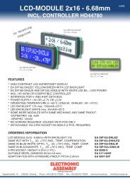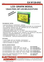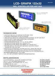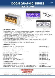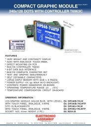
EA P128-6N7LED LCD- GRAFIK MODUL
EA P128-6N7LED LCD- GRAFIK MODUL
EA P128-6N7LED LCD- GRAFIK MODUL

You also want an ePaper? Increase the reach of your titles
YUMPU automatically turns print PDFs into web optimized ePapers that Google loves.
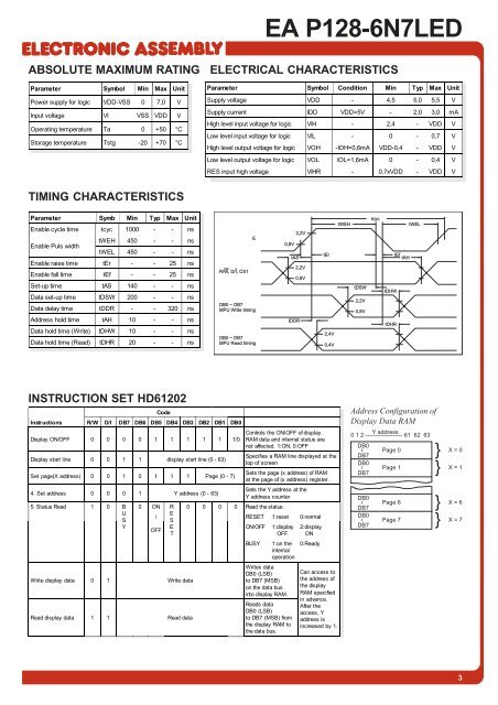
ABSOLUTE MAXIMUM RATING<br />
Parameter Symbol Min Max Unit<br />
Power supply for logic VDD-VSS 0 7,0 V<br />
Input voltage VI VSS VDD V<br />
Operating temperature Ta 0 +50 °C<br />
Storage temperature Tstg -20 +70 °C<br />
TIMING CHARACTERISTICS<br />
Parameter Symb Min Typ Max Unit<br />
Enable cycle time tcyc 1000 - - ns<br />
Enable Puls width<br />
tWEH 450 - - ns<br />
tWEL 450 - - ns<br />
Enable raise time tEr - - 25 ns<br />
Enable fall time tEf - - 25 ns<br />
Set-up time tAS 140 - - ns<br />
Data set-up time tDSW 200 - - ns<br />
Data delay time tDDR - - 320 ns<br />
Address hold time tAH 10 - - ns<br />
Data hold time (Write) tDHW 10 - - ns<br />
Data hold time (Read) tDHR 20 - - ns<br />
INSTRUCTION SET HD61202<br />
<strong>EA</strong> <strong>P128</strong>-<strong>6N7LED</strong><br />
ELECTRICAL CHARACTERISTICS<br />
Parameter Symbol Condition Min Typ Max Unit<br />
Supply voltage VDD - 4,5 5,0 5,5 V<br />
Supply current IDD VDD=5V - 2,0 3,0 mA<br />
High level input voltage for logic VIH - 2,4 - VDD V<br />
Low level input voltage for logic VIL - 0 - 0,7 V<br />
High level output voltage for logic VOH -IOH=0,6mA VDD-0,4 - VDD V<br />
Low level output voltage for logic VOL IOL=1,6mA 0 - 0,4 V<br />
RES input high voltage VIHR - 0,7xVDD - VDD V<br />
R/W, D/I, CS1<br />
E<br />
DB0 ~ DB7<br />
MPU Write timing<br />
DB0 ~ DB7<br />
MPU Read timing<br />
Code<br />
Instructions R/W D/I DB7 DB6 DB5 DB4 DB3 DB2 DB1 DB0<br />
Display ON/OFF 0 0 0 0 1 1 1 1 1 1/0<br />
Controls the ON/OFF of display.<br />
RAM data and internal status are<br />
not affected. 1:ON, 0:OFF<br />
Display start line 0 0 1 1 display start line (0 - 63)<br />
Specifies a RAM line displayed at the<br />
top of screen<br />
Set page(X address) 0 0 1 0 1 1 1 Page (0 - 7)<br />
Sets the page (x address) of RAM<br />
at the page of (x address) register.<br />
4. Set address 0 0 0 1 Y address (0 - 63)<br />
Sets the Y address at the<br />
Y address counter<br />
5. Status Read 1 0 B 0 ON R 0 0 0 0 Read the status.<br />
U<br />
S<br />
/<br />
E<br />
S<br />
RESET 1:reset 0:normal<br />
Y<br />
OFF<br />
E<br />
T<br />
ON/OFF 1:display<br />
OFF<br />
2:display<br />
ON<br />
BUSY 1:on the<br />
internal<br />
operation<br />
0:Ready<br />
Writes data<br />
DB0 (LSB) Can access to<br />
Write display data<br />
Read display data<br />
0<br />
1<br />
1<br />
1<br />
Write data<br />
Read data<br />
to DB7 (MSB)<br />
on the data bus<br />
into display RAM.<br />
Reads data<br />
DB0 (LSB)<br />
to DB7 (MSB) from<br />
the display RAM to<br />
the data bus.<br />
the address of<br />
the display<br />
RAM specified<br />
in advance.<br />
After the<br />
access, Y<br />
address is<br />
increased by 1.<br />
0,8V<br />
tAS<br />
2,2V<br />
2,2V<br />
0,8V<br />
tDDR<br />
tEr tEf<br />
tAH<br />
2,4V<br />
0,4V<br />
tWEH<br />
tDSW<br />
2,2V<br />
0,8V<br />
Address Configuration of<br />
Display Data RAM<br />
0 1 2 -------------------<br />
Y address<br />
61 62 63<br />
DB0<br />
DB7<br />
Page 0<br />
DB0<br />
DB7<br />
Page 1<br />
~<br />
~<br />
DB0<br />
DB7<br />
DB0<br />
DB7<br />
~<br />
~<br />
tcyc<br />
tDHW<br />
tDHR<br />
Page 6<br />
Page 7<br />
tWEL<br />
}<br />
}<br />
}<br />
}<br />
X = 0<br />
X = 1<br />
X = 6<br />
X = 7<br />
3