Master Equation - Based Numerical Simulation in a Single Electron ...
Master Equation - Based Numerical Simulation in a Single Electron ...
Master Equation - Based Numerical Simulation in a Single Electron ...

You also want an ePaper? Increase the reach of your titles
YUMPU automatically turns print PDFs into web optimized ePapers that Google loves.
252<br />
6. Examples of simulated results<br />
<strong>Numerical</strong> <strong>Simulation</strong>s of Physical and Eng<strong>in</strong>eer<strong>in</strong>g Processes<br />
Two examples will be used to demonstrate the numerical solution of <strong>Master</strong> equation <strong>in</strong><br />
s<strong>in</strong>gle electron transistor.<br />
Example 1:<br />
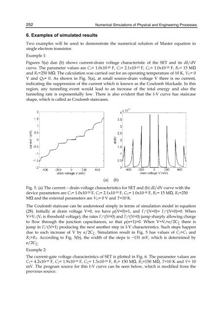
Figures 5(a) dan (b) shows current-dra<strong>in</strong> voltage characteristic of the SET and its dI/dV<br />
curve. The parameter values are C1= 1.0x10⁻²⁰ F, C2= 2.1x10⁻¹⁹ F, CG= 1.0x10⁻¹⁸ F, R1= 15 MΩ<br />
and R2=250 MΩ. The calculation was carried out for an operat<strong>in</strong>g temperature of 10 K, VG= 0<br />
V and Q0= 0. As shown <strong>in</strong> Fig. 5(a), at small source-dra<strong>in</strong> voltage V there is no current,<br />
<strong>in</strong>dicat<strong>in</strong>g the suppression of the current which is known as the Coulomb blockade. In this<br />
region, any tunnel<strong>in</strong>g event would lead to an <strong>in</strong>crease of the total energy and also the<br />
tunnel<strong>in</strong>g rate is exponentially low. There is also evident that the I-V curve has staircase<br />
shape, which is called as Coulomb staircases.<br />
(a) (b)<br />
Fig. 5. (a) The current – dra<strong>in</strong> voltage characteristics for SET and (b) dI/dV curve with the<br />
device parameters are C1= 1.0x10 -20 F, C2= 2.1x10 -19 F, CG= 1.0x10 -18 F, R1= 15 MΩ, R2=250<br />
MΩ and the external parameters are VG= 0 V and T=10 K.<br />
The Coulomb staircase can be understood simply <strong>in</strong> terms of simulation model <strong>in</strong> equation<br />
(28). Initially at dra<strong>in</strong> voltage V=0, we have ρ(N=0)=1, and Γ1 +(N=0)= Γ2 +(N=0)=0. When<br />
V=Vt (Vt is threshold voltage), the rates Γ1 +(N=0) and Γ2 +(N=0) jump sharply allow<strong>in</strong>g charge<br />
to flow through the junction capacitances, so that ρ(n=1)>0. When V=Vt+e/2C∑ there is<br />
jump <strong>in</strong> Γ1 +(N=1) produc<strong>in</strong>g the next another step <strong>in</strong> I-V characteristics. Such steps happen<br />
due to each <strong>in</strong>crease of V by e/2C∑. <strong>Simulation</strong> result <strong>in</strong> Fig. 5 has values of C2>C1 and<br />
R2>R1. Accord<strong>in</strong>g to Fig. 5(b), the width of the steps is ~131 mV, which is determ<strong>in</strong>ed by<br />
e/2C∑.<br />
Example 2:<br />
The current-gate voltage characteristics of SET is plotted <strong>in</strong> Fig. 6. The parameter values are<br />
C1= 4.2x10⁻¹⁹ F, C2= 1.9x10⁻¹⁸ F, CG= 1.3x10⁻¹⁸ F, R1= 150 MΩ, R2=150 MΩ, T=10 K and V= 10<br />
mV. The program source for this I-V curve can be seen below, which is modified from the<br />
previous source.