Master Equation - Based Numerical Simulation in a Single Electron ...
Master Equation - Based Numerical Simulation in a Single Electron ...
Master Equation - Based Numerical Simulation in a Single Electron ...

Create successful ePaper yourself
Turn your PDF publications into a flip-book with our unique Google optimized e-Paper software.
240<br />
<strong>Numerical</strong> <strong>Simulation</strong>s of Physical and Eng<strong>in</strong>eer<strong>in</strong>g Processes<br />
voltage, the Coulomb blockade is defeated and the electrons can tunnel through the junctions<br />
and f<strong>in</strong>ally the current flows. If the island between two tunnel junctions is electrostatically<br />
controlled by the gate capacitance, the system became s<strong>in</strong>gle electron transistor. This device is<br />
rem<strong>in</strong>iscent of a MOSFET, but with a small island (dot) embedded between two tunnel<br />
capacitors/junctions, <strong>in</strong>stead of the usual <strong>in</strong>version channel.<br />
It is well known that a numerical simulation of the devices could help a great deal <strong>in</strong> their<br />
understand<strong>in</strong>g of the devices. However, although so far several groups have reported the<br />
simulation and model<strong>in</strong>g of s<strong>in</strong>gle electron tunnel<strong>in</strong>g devices (Amman et al., 1991; Kirihara et<br />
al., 1994; Fonseca et al., 1997; Wasshuber et al., 1997; Nuryadi et al., 2010), numerical<br />
simulation with detail explanation and easy examples is still needed, especially for beg<strong>in</strong>ners<br />
<strong>in</strong> the field of s<strong>in</strong>gle electron devices. Basically there are two methods to simulate the s<strong>in</strong>gle<br />
electron phenomena, i.e., master equation (Amman et al., 1991; Nuryadi et al., 2010) and<br />
Monte Carlo methods (Kirihara et al., 1994; Fonseca et al., 1997; Wasshuber et al., 1997).<br />
The goal of this chapter is to simulate numerically current-voltage characteristics <strong>in</strong> the<br />
s<strong>in</strong>gle electron transistor based on master equation. A master equation for the probability<br />
distribution of electrons <strong>in</strong> the SET dot (see Fig. 1) is obta<strong>in</strong>ed from the stochastic process,<br />
allow<strong>in</strong>g the calculation of device characteristics. First, I will start with an <strong>in</strong>troduction of<br />
the basic equations <strong>in</strong> <strong>Master</strong> equation (section II). Next, the derivation of free energy<br />
change due to electron tunnel<strong>in</strong>g event is discussed <strong>in</strong> section III. The flowchart of<br />
numerical simulation based on <strong>Master</strong> equation and the Matlab implementation will be<br />
discussed <strong>in</strong> section IV and V, respectively. The examples of simulation resuls are presented<br />
<strong>in</strong> section V. F<strong>in</strong>ally, section VI is conclusion.<br />
2. Basic equations <strong>in</strong> master equation based simulation<br />
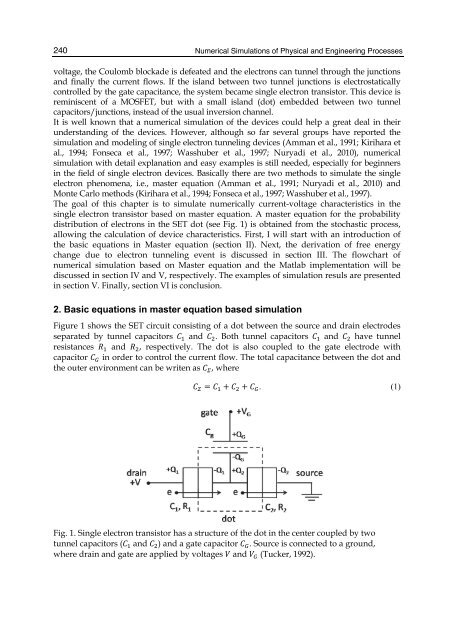
Figure 1 shows the SET circuit consist<strong>in</strong>g of a dot between the source and dra<strong>in</strong> electrodes<br />
separated by tunnel capacitors and . Both tunnel capacitors and have tunnel<br />
resistances and , respectively. The dot is also coupled to the gate electrode with<br />
capacitor <strong>in</strong> order to control the current flow. The total capacitance between the dot and<br />
the outer environment can be writen as , where<br />
= + + . (1)<br />
Fig. 1. S<strong>in</strong>gle electron transistor has a structure of the dot <strong>in</strong> the center coupled by two<br />
tunnel capacitors ( and ) and a gate capacitor . Source is connected to a ground,<br />
where dra<strong>in</strong> and gate are applied by voltages and (Tucker, 1992).