

Chapter 2 THE GENERAL INSTRUMENT CP1600 - Intellivision Brasil
Chapter 2 THE GENERAL INSTRUMENT CP1600 - Intellivision Brasil
Chapter 2 THE GENERAL INSTRUMENT CP1600 - Intellivision Brasil

Create successful ePaper yourself
Turn your PDF publications into a flip-book with our unique Google optimized e-Paper software.
<strong>Chapter</strong> 2<br />
<strong>THE</strong> <strong>GENERAL</strong> <strong>INSTRUMENT</strong> <strong>CP1600</strong><br />
The <strong>CP1600</strong> and the TMS 9900 were the first two NMOS16-bit microprocessors commercially available.<br />
Even a superficial inspection of the <strong>CP1600</strong> shows It to be more powerful than the National Semiconductor<br />
PACE (Or 8900), yet the <strong>CP1600</strong> is not widely used. This is because General Instrument does not support<br />
the <strong>CP1600</strong> to the extent that National Semiconductor originally supported PACE, or most manufacturers support<br />
their 8-bit microprocessors.<br />
General Instrument's marketing philosophy has been to seek out very high volume customers: General<br />
Instrument supports low-volume customers only to the extent that this support would not require substantial<br />
investment on the part of General Instrument.<br />
From the viewpoint of the low-volume microprocessor user. General Instrument's marketing philosophy is unfortunate.<br />
The <strong>CP1600</strong> is an ideal microprocessor for the more sophisticated video games that are appearing, and<br />
its rich Instruction set and capable architecture make it an ideal choice for data processing terminals and home<br />
computer systems However, due to it’s limited support, potential low-volume <strong>CP1600</strong> customers are Iikely to<br />
choose another equally capable product.<br />
Three <strong>CP1600</strong> parts are available, differentiated only by the clock speeds for which they have been<br />
designed.<br />
The <strong>CP1600</strong> requires a 3.3 MHz. two-phase clock and generates a 600 nanosecond machine cycle time.<br />
The <strong>CP1600</strong> requires a 4 MHz. two-phase clock and generates a 500 nanosecond machine cycle time.<br />
The CP1610 requires a 2 MHz. two-phase clock and generates a 1 microsecond cycle time.<br />
In addition to the <strong>CP1600</strong> microprocessors themselves, the CP1680 Input/0utput Buffer (IOB) is<br />
described in this chapter. Additional support devices for the <strong>CP1600</strong> may be found in An Introduction<br />
to Microcomputers: Volume 3 – Some Real Support Devices.<br />
The sole source for the <strong>CP1600</strong> is:<br />
<strong>GENERAL</strong> <strong>INSTRUMENT</strong><br />
Microelectronics Division<br />
600 West John Street<br />
Hicksville, New York 11802<br />
There is no second source for the <strong>CP1600</strong>. General Instrument has a policy of discouraging second sources<br />
for its product line.<br />
The <strong>CP1600</strong> is fabricated using NMOS ion implant LSI technology; the device is packaged as a 40-pin DIP.<br />
Three power supplies are required: +12V, +5V, and -3V.<br />
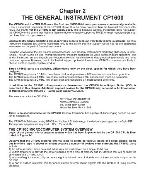
<strong>THE</strong> <strong>CP1600</strong> MICROCOMPUTER SYSTEM OVERVIEW<br />
Logic of our general microcomputer system which has been implemented by the <strong>CP1600</strong> CPU is illustrated<br />
in Figure 2-1.<br />
Observe that the <strong>CP1600</strong> requires external logic to create its various timing and clock signals. Some<br />
bus interface logic is shown as absent because a number of devices must surround the <strong>CP1600</strong>: these<br />
include:<br />
1) An address buffer, since data and addresses are multiplexed on a single 16-bit bus.<br />
2) Buffer amplifiers to provide the power required by the type of memory and l/O devices that will normally be<br />
connected to a <strong>CP1600</strong> CPU.<br />
3) A one-of-eight decoder chip to create eight individual control signals out of three controls output by the<br />
<strong>CP1600</strong>.<br />
4) A one-of-sixteen multiplex chip to funnel sixteen external status signals into the <strong>CP1600</strong> if using external<br />
branches.
Were you to compare Figure 2-1 with an equivalent figure for a low-end microprocessor such as the SC/MP<br />
(which is described In <strong>Chapter</strong> 3 of the Osborne 4 & 8-Bit Microprocessor Handbook (Osborne/McGraw-Hill,<br />
1980), the <strong>CP1600</strong> might appear to offer fewer logic functions: but within the functions it does provide the<br />
<strong>CP1600</strong> provides considerably more logic and program execution capabilities. Where low-end microprocessors<br />
choose to condense onto a single chip, simple implementations of different logic functions, high-end products<br />
such as the <strong>CP1600</strong> choose to provide more devices greater capabilities on each device.<br />
Logic to Handle<br />
Intrrupt Rquests from<br />
External Devices<br />
Interrupt Priority<br />
Arbitration<br />
I/O Communication<br />
Serial to Parallel<br />
Interface Logic<br />
Programmable<br />
Timers<br />
Clock Logic<br />
Arithmetic and Logic<br />
Unit<br />
Instruction Register<br />
Control Unit<br />
Bus Interface Logic<br />
System Bus<br />
ROM addressing and<br />
Interface Logic<br />
Read Only Memory<br />
Accumulator<br />
Register(s)<br />
Data Counter(s)<br />
Stack Pointer<br />
Program Counter<br />
I/O Ports<br />
Interface Logic<br />
I/O Ports<br />
Figure 2-1. Logic of the <strong>CP1600</strong> CPU and CP1680 I/O Buffer<br />
Direct Memory<br />
Access Control Logic<br />
RAM addressing<br />
and<br />
Interface Logic<br />
Read/Write<br />
Memory<br />
<strong>CP1600</strong> CPU<br />
CP1680 I/O Buffer
<strong>CP1600</strong> PROGRAMMABLE REGISTERS<br />
The <strong>CP1600</strong> has eight 16-bit programmable registers, which may be illustrated as follows:<br />
The way in which the registers illustrated above are used is unusual when compared to other microcomputers<br />
described in this book. All eight 16-bit registers can be addressed as though they were general purpose registers:<br />
however, only Register R0 has no other assigned function. We may therefore look upon Register R0 as the<br />
Primary Accumulator for this CPU.<br />
Registers R1, R2, and R3 serve as general purpose registers, But may also be used as Data Counters.<br />
In addition to serving as general purpose registers, R4 and R5 may be used as auto-incrementing Data<br />
Counters. Memory reference instructions that identify Register R4 or R5 as holding the implied memory address<br />
will cause the contents of Register R4 or R5 to be incremented — after the memory reference instructions have<br />
completed execution.<br />
Registers R6 and R7, in addition to being accessible as general purpose registers, also serve as a Stack Pointer<br />
and a Program Counter, respectively.<br />
Having the Stack Pointer accessible as a general purpose register makes it quite simple to maintain more that<br />
one Stack in external memory; also, you can easily address the Stack as data memory using the Stack Pointer<br />
as a Data Counter.<br />
Having the Program Counter accessible as a general purpose register can be useful when executing various<br />
types of conditional branch logic.<br />
While having the Stack Pointer and the Program Counter accessible as though they were general purpose registers<br />
may appear strange, this is a feature of the PDP-11 minicomputer — and is a very powerful programming<br />
tool.<br />
<strong>CP1600</strong> MEMORY ADDRESSING MODE<br />
The <strong>CP1600</strong> addresses memory and I/O devices within a single address space.<br />
When referencing external memory, you can use direct addressing, implied addressing, or implied<br />
addressing with auto-increment.<br />
Direct addressing instructions are all two or more words long, where the<br />
second or last word of the instruction object code provides a I6-bit direct<br />
address.<br />
<strong>CP1600</strong> DIRECT<br />
ADDRESSING<br />
<strong>CP1600</strong> direct addressing instructions are complicated by the fact that <strong>CP1600</strong> program memony is frequently<br />
only 10 bits wide. That is to say, even though the <strong>CP1600</strong> is a 16-bit microprocessor, its instruction object codes<br />
are only 10 bits wide. If program memory is only 10 bits wide, then direct addresses will only be 10 bits wide. A<br />
10-bit direct address will access the first 1024 words of memory only.<br />
R0<br />
R1<br />
R2<br />
R3<br />
R4<br />
R5<br />
R6<br />
R7<br />
Data Counters<br />
Data Counters with<br />
auto-increment<br />
Stack Pointer<br />
Program Counter<br />
General Purpose registers
Were you to implement a 16-bit wide program memory, then you could directly address up to 65.536 words of<br />
memory, however, six bits of the first object program word for every instruction in program memory would be<br />
wasted. This may be illustrated as follows:<br />
Instructions that reference memory using implied addressing identify<br />
general purpose Register R1, R2, or R3 as containing the implied<br />
address.<br />
<strong>CP1600</strong><br />
IMPLIED<br />
ADDRESSING<br />
A memory reference instruction which identifies Register R4 or R5 as providing<br />
the external memory address will always cause Register R4 or R5 contents to be incremented following the<br />
memory access; thus you have implied memory addressing with auto-increment.<br />
Memory reference instruction, that specify implied memory addressing via Register 1, 2, 3, 4, or 5 can<br />
access 8-bit memory. An SDBD instruction executed directly before a valid memory reference instruction<br />
forces the reference instruction to access memory one byte at a time if implied memory addressing via Register<br />
1, 2, or 3 is specified, then the same byte of memory will be accessed twice For an instruction that loads the<br />
contents of data memory into Register R0, this may be illustrated as follows:
If Registers R4 or R5 provides the implied memory address for the instruction which follows an SDBD instruction,<br />
then the implied memory address is incremented twice, and two sequential low-order bytes of data are<br />
accessed. For an Instruction which loads data into Register R0, this may be illustrated as follows:<br />
The SDBD instruction may also precede an immediate Instruction. Now the immediate data will be fetched from<br />
the low-order byte of the next two sequential program memory locations This may be illustrated as foilows<br />
Without the preceding SDBD instruction, an immediate instruction will access the next single program memory<br />
word to find the required immediate data. Ten or more bits of immediate data will be accessed depending on<br />
the width of program memory words.<br />
The <strong>CP1600</strong> has no Stack reference instructions such as a Push or Pull;<br />
rather, a variety of memory reference instructions can identify Register R6<br />
as providing the implied address. When Register R6 provides the implied<br />
address, it is treated as an upward migrating Stack Pointer. When a memory write<br />
operation specifies Register R6 as providing the implied memory address,<br />
Register R6 contents will be incremented following the memory write. A memory<br />
<strong>CP1600</strong> STACK<br />
ADDRESSING<br />
read instruction that specifies Register R6 as providing the implied memory address will cause the contents of<br />
Register R6 to be decremented before the read operation occurs.<br />
An unusual feature of the <strong>CP1600</strong> is the fact that a variety of secondary memory reference instructions<br />
can also be reference memory via the Stack Pointer. When these instructions are executed. Register R6<br />
contents are decre mented before the memory access occurs — as though a Pull operation from the Stack were<br />
being executed.<br />
Logically, Register R6, the Stack Pointer, is being handled as though it were a Data Counter with post-increment<br />
and pre-decrement.
Jump instructions use direct memory addressing. Jump instructions are all three words long. The direct address<br />
is computed from the second and third memory words as follows:<br />
AAAAAABBBBBBBBBB Jump address (binary)<br />
YY are enable/disable bits for interrupts<br />
XX identity the register where the return address will be stored for JSR<br />
XX and YY are described in detail in Table 2-4.<br />
You can enable or disable interrupts whenever you execute a Jump or Jump-to-Subroutine instruction.<br />
The only difference between a Jump instruction and a Jump-to-Subroutine instruction is that the Jump-to-<br />
Subroutin instruction saves the Program Counter contents in Register 4, 5, or 6. The two high-order bits (XX) or<br />
the second Jump-to-Subroutine obect code word specifies which of the three registers will be used to hold the<br />
return address.<br />
Jump-to-Subroutine instructions, like the Jump instruction, allow direct memory addressing only.<br />
<strong>CP1600</strong> STATUS AND CONTROL FLAGS<br />
The <strong>CP1600</strong> CPU has four of the standard status flags; in addition, it has some unusual control signals.<br />
These are the four standard status flags:<br />
Sign (S). This status is set equal to the high-order bit of any arithmetic operation result.<br />
Zero (Z). This status is set to 1 when any instruction’s execution creates a zero result. The status is set to 0 for<br />
a nonzero result.<br />
The Carry (C) and Overflow (O) statuses are standard carry and overflow, as described in Volume 1.<br />
Four control signals (EBCA0 - EVCA3) are output during a Branch-on-External (BEXT) instruction. These<br />
four signals are output to reflect the low-order four bits of the BEXT instruction’s object code. External logic<br />
receives these four signals and (depending on their state), may or may not return a high input via EBCI. If EBCI<br />
is returned high, then the BEXT instruction will perform a branch; if EBCI is returned low, then the BEXT instruction<br />
will cause the next sequential instruction to be executed. The four control signals EBCA0 - EBCA3 therefore<br />
provide the <strong>CP1600</strong> with a means of testing 16 external conditions.<br />
<strong>CP1600</strong> CPU PINS AND SIGNALS<br />
9 8 7 6 5 4 3 2 1 0<br />
0 0 0 0 0 0 0 1 0 0<br />
X X A A A A A A Y Y<br />
B B B B B B B B B B<br />
<strong>CP1600</strong> CPU pins and signals are illustrated in Figure 2-2.<br />
JR or JSR<br />
D0 - D15 is a multiplexed Address and Data Bus. Given a total of 40 pins in a package, <strong>CP1600</strong> designers<br />
have been forced to share 16 pins between addresses and data. Three control signals BDIR, BC1, and BC2,<br />
identify the traffic on the Address/Data Bus. External logic (one MSI chip) must decode these three signals<br />
to create eight control signals, as summarized in Table 2-1.<br />
Remaining signals may be divided into four groups: timing, status/control, interrupt, and DMA.<br />
Two timing clock signals are required: F1 and F2. These are complementary clock signals which may be<br />
illustrated as follows:<br />
F1<br />
F2<br />
Word 2<br />
Word 3
Figure 2-2 <strong>CP1600</strong> CPU Signals and Pin Assignments<br />
MSYNC is a somewhat unusual signal, as compared to other microcomputer clock signals in this book.<br />
Following powerup. MSYNC must be held low for at least 10 milliseconds. On the subsequent rising edge<br />
of MSYNC, logic internal to the <strong>CP1600</strong> CPU will synchronize the F1 and F2 clock signals to start a new<br />
machine cycle. Most of the CPU devices we have described in this book use a reset signal or have internal<br />
powerup logic which performs this clock synchronization.<br />
Now consider the status and control signals.<br />
First of all, there are the four control outputs which we have already described: EBCA0 - EBCA3. There is<br />
one conditional Branch instruction (BEXT) which will only branch if a high signal is input via EBCI.<br />
When the BEXT instruction is executed, the low-order four BEXT instruction object code bits are output via<br />
EBCA0 - EBCA3. External logic is supposed to decode these four signals by whatever means are appropriate<br />
— and thence determine whether EBCI shouId be input high or low. A high input, as we have just stated, will<br />
result in a branch; a low input wiII cause the next sequential instruction to be executed.<br />
In reality, there is no connection within <strong>CP1600</strong> CPU logic between the EBCI input and the four EBCA0-EBCA3<br />
outputs. So far as external logic is concerned, the execution of a BEXT instruction is identified by signal levels<br />
output and maintained on the EBCA0 - EBCA3 outputs. While the EBCI input determines whether a branch will<br />
or will not occur. How external logic chooses to determine whether EBCI will be set high or low is entirely up to<br />
external logic. The only vital function served by EBCA0 - EBCA3 is to identify the instant at which a BEXT<br />
instruction is executed.<br />
Another unusual control signal provided by the <strong>CP1600</strong> is PCIT: this is a bidirectional signal. When input<br />
low, this signal prevents the Program Counter from being incremented following an instruction fetch. This signal<br />
is also output as a low pulse following execution of a software interrupt instruction. Instruction timing separates<br />
the active input and
active output of this signal; providing external logic adheres to timing requirements, a conflict between input and<br />
output logic will never arise.<br />
BDRDY is equivalent to the WAIT signal we have described for a number of other microcomputers.<br />
BDRDY is input low by any external logic which requires more time in order to respond to an I/O access. Recall<br />
that the <strong>CP1600</strong> uses a single address space to reference memory or I/O devices. The BDRDY signal causes<br />
the CPU to enter a Wait state for as long as BDRDY is being input low; however, during the Wait state, CPU<br />
logic is not refreshed. Thus a Wait state cannot last for more than 40 microseconds, or the contents of internal<br />
CPU locations will be lost.<br />
STPST a Halt/Reset input, is an edge-triggered signal. When external logic inputs a high-to-low transition via<br />
STPST the CPU will complete execution of any interrupt instruction, then will enter a Halt state and output HALT<br />
high. If a non-interruptable instruction is being executed, then the Halt state will not begin until completion of<br />
next interruptabel instruction's execution. The Halt state will last until external logic inputs another high-to-low<br />
STPST transition, at which time the Halt output will be returned low and normal programming execution will continue.<br />
Execution of the HLT instruction also causes the <strong>CP1600</strong> to enter a Halt state as described above.<br />
Let us now look at interrupt signals.<br />
The <strong>CP1600</strong> has two interrupt request inputs — INTR and INTRM. INTR has higher priority than INTRM<br />
INTR cannot be disabled. Typically, INTR will be used to trigger an interrupt upon power failure or other catastrophes.<br />
The interrupt acknowledge signal is created by external logic which must decode the BC1, BC2, and<br />
BDIR signals, as shown in Table 2-1. Observe that there are, in fact, two interrupt acknowledge signals: the first<br />
(INTAK) acknowledges the interrupt itself, while the second (DAB) is used as a strobe for external logic to return<br />
an interrupt address vector. The interrupt sequence is described later in this chapter.<br />
The <strong>CP1600</strong> has two additional interrupt related signals which are unusual compared to other microcomputers<br />
described in this book.<br />
TCI is output high when an End-of-Interrupt Instruction is executed. This signal makes it easy for external logic<br />
to generate interrupt priorities which extend across the execution of an interrupt service routine.<br />
Table 2-1, <strong>CP1600</strong> Bus Control Signals<br />
BC1 BC2 BDIR SIGNAL FUNCTION<br />
0 0 0 NACT The CPU is inactive and the Data/Address Bus is in a<br />
high impedance state.<br />
0 0 1 BAR A memory address must be input to the CPU via the<br />
Data/Address Bus.<br />
0 1 0 IAB Acknowledged external interrupt requesting logic must<br />
place the starting address for the interrupt service routine<br />
on the Address Bus.<br />
0 1 1 DWS Data write strobe for external memory.<br />
1 0 0 ADAR This signal identifies a time interval during which the<br />
Data/Address Bus is floated, while data input on the<br />
Data Bus is being interpreted as the effective memory<br />
address during a direct memory addressing operation.<br />
1 0 1 DW The CPU is writing data into external memory. DW will<br />
precede DWS by one machine cycle.<br />
1 0 0 DTB This is a read strobe which external memory or I/O logic<br />
can use in order to place data on the Data/Address Bus.<br />
1 1 1 INTAK This is an interrupt acknowledge signal. It is followed by<br />
IAD which is a strobe telling the external logic which is<br />
being acknowledged to identify itself by placing an<br />
address vector on the Data/Address Bus.
Figure 2-3. <strong>CP1600</strong> Machine Cycles and Buss Timing<br />
Figure 2-4. <strong>CP1600</strong> Instruction Fetch Timing
Figure 2-5. <strong>CP1600</strong> Timing for Memory Read Instruction with Implied Memory Addressing<br />
<strong>CP1600</strong> INSTRUCTION TIMING AND EXECUTION<br />
<strong>CP1600</strong> instructions are executed as a sequence of machine cycles. Each machine cycle has four<br />
clock periods, as illustrated in Figure 2-3. Machine cycles are identified by their cycle number and by the<br />
levels of the BC1, BC2, and BDIR signals. Each of the eight level combinations is given a name, taken from<br />
Table 2-1. This name becomes the name of the machine cycle. Thus in Figure 2-4. and in subsequent instruction<br />
timing iilustrations, each machine cycle is identified by a signal name from Table 2-1.<br />
Figure 2-3 shows general case timing for data output or input on the Data/Address Bus. In between data input<br />
or output operations the bus is floated.<br />
<strong>CP1600</strong> MEMORY ACCESS TIMING<br />
Figure 2-4 illustrates instruction fetch timing for a <strong>CP1600</strong> instruction’s execution. Three machine<br />
cycles are required. During the first machine cycle an address is output. Nothing happens during the second<br />
machine cycle; it is a "time spacing" machine cycle that routinely separates two <strong>CP1600</strong> Bus access machine<br />
cycles. The object code for the accessed instruction is returned during the third machine cycle.<br />
Figure 2-5 illustrates timing for the simplest memory read instruction’s execution. In this case the data<br />
memory address is taken from one of the CPU registers. There is no difference between timing for the three<br />
machine cycles of an instruction fetch or a data memory read. As illustrated in Figure 2-5, a simple memory<br />
read instruction's execution consists of two three-machine cycle memory read operations, separated by a<br />
spacing no operation machine cycle.
Figure 2-6 <strong>CP1600</strong> Timing for Memory Write Instruction with Implied Memory Addressing<br />
Figure 2-6 illustrates timing for a simple <strong>CP1600</strong> memory write instruction execution. Data is output for<br />
two machine cycles, giving external logic ample time to respond to the data output cycle as a write strobe.<br />
Any memory reference instruction that specifes direct memory addressing will require one three-clock-period<br />
machine cycle to fetch each word of the instruction object code; an NACT clock period will separate each<br />
machine cycle. After the first instruction fetch machine cycle an ADAR-NACT clock period combination will be<br />
inserted in the second (and third, if present) instruction fetch machine cycle. During an ADAR clock period.<br />
BC1 is high, while BC2 and BDIR are low. No other control signals are active. Thus, for a two-word memory<br />
read or memory write instruction that specifies direct addressing, the following clock periods and<br />
machine cycles will be required for instruction execution:<br />
Direct addressing Direct addressing<br />
Memory Read Memory Write<br />
Machine Cycles Machine Cycles<br />
BAR Fetch first instruction BAR<br />
NACT object code word NACT<br />
DTB DTB<br />
NACT Spacing machine cycle NACT<br />
BAR BAR<br />
NACT NACT<br />
ADAR Fetch second instruction ADAR<br />
NACT object code word NACT<br />
DTB DTB<br />
NACT Spacing machine cycle NACT<br />
BAR Memory read Memory write BAR<br />
NACT machine cycle machine cycle NACT<br />
DTB DW<br />
DWS
<strong>THE</strong> <strong>CP1600</strong> WAIT STATE<br />
Figure 2-7 <strong>CP1600</strong> Wait State Timing<br />
The <strong>CP1600</strong> has a Wait state equivalent to those described for other microcomputers in this book. ExternaI<br />
logic that requires more time to respond to an access must input BDRDY low before the end of the BAR<br />
machine cycle, during which an address is output and the device is selected. Timing is illustrated in Figure 2-7.<br />
If you examine Figures 2-4, 2-5, and 2-6, you will see that an address is output during a BAR machine cycle<br />
to initiate any external device access. The BAR machine cycle is always followed by an NACT machine cycle;<br />
in the middle of T1 during this NACT machine cycle, the <strong>CP1600</strong> samples BDRDY. If BDRDY is low then a<br />
sequence of NACT machine cycles occurs in the middle of T4 for every NACT machine cycle, the <strong>CP1600</strong><br />
samples BDRDY again. Upon detecting BDRDY high, the <strong>CP1600</strong> resumes instruction execution with a DTB<br />
machine cycle.<br />
A Wait state must last for less than 40 microseconds, since the <strong>CP1600</strong> is a dynamic device.<br />
<strong>THE</strong> <strong>CP1600</strong> HALT STATE<br />
The <strong>CP1600</strong> has a Halt state which may follow execution of the Halt instruction, or may be initiated by<br />
external logic.<br />
When the Halt instruction is executed, then, following the instruction fetch machine cycle, the HALT signal is<br />
output high and a sequence of NACT machine cycles is executed.<br />
External logic initiates a Halt state by making the STPST input undergo a high-to-low transition. Following<br />
execution of the next interruptable instruction, a Halt state begins. The HALT signal is output high and a<br />
sequence of NACT machine cycles is executed.<br />
A Halt state, whether it is initiated by execution of a Halt instruction or by a high-to-low transition of STPST.<br />
must be terminated by a high-to-low transition of STPST. This will cause the Halt state to end at the conclusion<br />
of the next NACT machine cycle. Timing for a Halt state which is initiated and terminated by STPST may<br />
be illustrated as follows:
The PCIT signal as an input inhibits <strong>CP1600</strong> Program Counter increment logic. Thus, external logic can<br />
input PCIT low — in which case the same instruction will be continuously re-executed unlil PCIT goes high<br />
again However, PCIT should only change levels while the CPU has been halted Thus, PCIT and STPST<br />
should be used together as follows:<br />
<strong>CP1600</strong> INITIALIZATION SEQUENCE<br />
The <strong>CP1600</strong> is initialited by inputting the MSYNC signal low for a minimum of 10 milliseconds after<br />
power is first applied to the CPU.<br />
MSYNC must make a low-to-high transition, marking the end of the initialization, on a rising edge of the F1<br />
clock signal. On the next rising edge of F1, instruction execution will begin. This may be illustrated as follows:<br />
When instruction execution begins, interrupts are disabled. The following sesuence of machine cycles is<br />
excuted:<br />
NACT<br />
IAB Read Data/Address Bus and load into Program Counter<br />
NACT<br />
NACT<br />
NACT<br />
BAR Output Program Counter contents to fetch first instruction<br />
NACT<br />
DTB<br />
During the IAB machine cycle, external logic must supply a 16-bit address at D0 - D15. Your external logic<br />
must provide this address, which in the simplest case may be 0000 by grounding the bus. or FFFF 16 by tying<br />
it to +5V following a startup.<br />
The address which is input at IAB is output at BAR, initiating program execution.<br />
<strong>CP1600</strong> DMA LOGIC<br />
<strong>CP1600</strong> DMA logic is quite standard. When external logic wishes to transfer data under DMA control it<br />
inputs BUSRQ low. At the conclusion of the next interruptable instruction’s execution, the CPU floats<br />
the Data/Address Bus and enters a Wait state, during which a sequence of NACT machine cycles is<br />
executed. BUSAK is output low at the beginning of the first NACT machine cycle.<br />
The NACT machine cycles that occur during a DMA operation refresh the CPU. NACT machine cycles<br />
that occur during a Wait state do not refresh the CPU. This means that any number of NACT machine cycles<br />
can occur during a DMA break, while a Wait state must be shorter than 40 microseconds.<br />
The DMA break ends when external logic inputs BUSRQ high again BUSRQ is sampled during T1 of every<br />
DMA NACT machine cycle. When BUSRQ is sampled high, two additional NACT machine cycles are executed,<br />
then BUSAK is output high and normal program execution resumes.
Figure 2-8. <strong>CP1600</strong> DMA Timing<br />
Figure 2-9. <strong>CP1600</strong> Interrupt Service Routine Initialization
<strong>THE</strong> <strong>CP1600</strong> INTERRUPT LOGIC<br />
Figure 2-10 <strong>CP1600</strong> Timing for TCI Instruction's Execution<br />
The <strong>CP1600</strong> uses a vectored interrupt processing system.<br />
External logic requests an interrupt by inputting a low signal at either the INTR or INTRM pins<br />
Following the execution of the next interruptable instruction, the <strong>CP1600</strong> acknowledges the interrupt by pushing<br />
Register R7 contents (the Program Counter) onto the Stack; then the <strong>CP1600</strong> outputs 111, followed by<br />
010 at BC1, BC2, and BDIR. External logic must respond by placing 16 bits of data on the Data/Address Bus<br />
These 16 bits of data will be loaded into Register R7, the Program Counter, thus causing program execution<br />
to branch to an interrupt service routine dedicated to the interrupt. Timing is illustrated in Figure 2-9.<br />
The PCIT signal is output low following execution of a software interrupt instruction (SIN). This is the only<br />
microcomputer described in this book which allows external logic to respond to a software interrupt in this<br />
fashion. Allowing external logic to respond to a software interrupt only makes sense when you anticipate your<br />
product being used in a minicomputer-like environment. Typically, the software interrupt will interface to logic<br />
of a front panel or console. When an SIN instruction is executed, a one-machine cycle low PCIT pulse is output.<br />
You may, if you wish end an interrupt service routine by executing a Terminate current Interrupt (TCI) instruction,<br />
in which case the TCI signal will be output high.<br />
Timing for TCI is given in Figure 2-10.<br />
Following an interrupt acknowledge, the interrupt service routine must execute instructions in order to disable<br />
interrupts and save the contents of registers on the Stack. The exception is Register R7, the prograim<br />
Counter, which is auto- matically pushed onto the Stack following an interrupt acknowledge.<br />
External logic is entirely responsible for any type of interrupt priority arbitration which may occur and for the<br />
generaion of the interrupt vector addresing which must be following an interrupt acknowledge.
It is quite easy to generate signals equivalent to other microcomputer system busses from the <strong>CP1600</strong><br />
System Bus. Therefore, you can use parts described in Volume 3 to handle <strong>CP1600</strong> interrupt requirements.<br />
<strong>THE</strong> <strong>CP1600</strong> INSTRUCTION SET<br />
The CP 1600 instruction set is relatively straight forward. Addressing modes, which we have already<br />
described, are simple, and instructions are typical of those we have seen and described for other microcomputers<br />
Unusual features relating to addressing modes available with individual instructions are summarized in<br />
Table 2-2, which describes the <strong>CP1600</strong> instruction set.<br />
If you have never programmed a PDP-11 minicomputer, then you should pay particular attention to<br />
programing techniques that result from the Stack Pointer and Program Counter being accessed as<br />
general purpose registers.<br />
A wide variety of Register Operate instructions allow you to compute data and load the result directly into<br />
Register R7, the Program Counter. In effect, these become computed Jump instructions.<br />
The ablilty to manipulate Register R6, the Stack Pointer, as though it were a general purpose register means<br />
that it is easy to maintain a number of different Stacks in external read/write memory<br />
The Jump-to-Subroutine instruction has a minicomputer flavor to it. Rather than saving the return address on<br />
the Stack, Register R7 contents are moved to General Purpose Register R4 or R5. A number of minicomputers<br />
will save a subroutine return address in a general purpose register in this fashion. The problem with this<br />
logic is that you must execute an additional instruction within the subroutine to save the return address on the<br />
Stack if you are going to use nesting subroutines. If you are passing subroutine parameters. however, this is<br />
an excellent arrangment, for the Jump-to-Subroutine instruction places the address of the parameter list<br />
directly in a Data Counter with auto-increment. We have described the concept of parameter passing in<br />
Volume 1, <strong>Chapter</strong> 7.<br />
Note that the <strong>CP1600</strong> instruction set lacks a logical OR.<br />
In Tables 2-2 and 2-4, instruction length is given in terms of "words” rather than “bytes”, as we have done in<br />
previous chapters. Since only the lower 10 bits of the <strong>CP1600</strong> object code are presently used, system configurations<br />
need not have the full 16-bit word size. Hence a "word" may be 10 to 16 bits wide, depending on the<br />
implementation.<br />
The following notation is used in table 2-2:<br />
ADDR One word of direct address.<br />
cond Condition on which a branch may be taken. Table 1-3 lists all 14 branch conditions.<br />
DATA One word of immediate data.<br />
DISP One word displacement. See Table 2-4 for location of sign bit.<br />
E External branch condition.<br />
EBCA0-3 The external branch condition address lines. EBAC0, EBAC1, EBAC2, EBAC3.<br />
EBCI The external branch condition input line.<br />
LABEL A 16-bit direct address, target of a Jump instruction. See Table 2-4 for the bit format.<br />
PCIT The software interrupt output line.<br />
RB General Purpose Register R4, R5, R6.<br />
RD One of the general purpose registers, used as destination for operation results.<br />
RM One of the general purpose registers used as a data counter, R4 or R5, if specified, is auto-incremented<br />
after memory access. R6 is incremented after a write, and decremented before a read.<br />
RR General Purpose Register R0, R1, R2, R3.<br />
RS One of the general purpose registers, used as the source of an operand.<br />
Statuses:<br />
S the Sign status<br />
C the Carry status<br />
Z the Zero status<br />
O the Overflow status<br />
The following symbols are used in the STATUSES collumn<br />
X the status flag is affected by the operation<br />
a blank means the status flag is not affected<br />
0 the operation clears the status flag<br />
1 the operation sets the status flag<br />
2 the overflow flag is affected only on 2-bit shifts or rotates
SW The Status Word, whose bits correspond to the condition of the status flags in the following<br />
way:<br />
When the status word is copied into a register, it goes to the upper half of each byte:<br />
When the status word is loaded from a register, it comes from the upper half of the lower byte:<br />
x Bits y through z of the Register x For example, R7 represents the upper byte of<br />
Program Counter<br />
(,2) Indicates that the operand “,2” is optional<br />
A low pulse<br />
[ ] Contents of location enclosed within brackets. If a register designation is enclosed within the<br />
brackets, then the designated registers contents are specified. If a memory address is<br />
enclosed within the brackets, then the contents of the addressed memory location are specified.<br />
[[ ]] Implied memory addressing, the contents of the memory location designated by the contents<br />
of a register.<br />
L Logical AND<br />
V Logical Exclusive-OR<br />
V Logical OR<br />
± Addition or subtraction of a displacement. depending on the sign bit in the object code.<br />
¬ Data is transferred in the direction of the arrow
TYPE<br />
PRIMARY I/O<br />
AND MEMORY<br />
REFRENCE<br />
SECONDARY I/O AND MEMORY REFERENCE<br />
MNEMONIC<br />
MVI<br />
MVI@<br />
MVO<br />
MVO@<br />
ADD<br />
ADD@<br />
SUB<br />
SUB@<br />
CMP<br />
CMP@<br />
AND<br />
AND@<br />
XOR<br />
XOR@<br />
OPERAND(S)<br />
ADDR, RD<br />
RM, RD<br />
RS, ADDR<br />
RS, RM<br />
ADDR, RD<br />
RM, RD<br />
ADDR, RD<br />
RM, RD<br />
ADDR, RS<br />
RM, RS<br />
ADDR, RD<br />
RM, RD<br />
ADDR, RD<br />
RM, RD<br />
Table 2-2. <strong>CP1600</strong> Instruct Set Summary<br />
WORDS<br />
2<br />
1<br />
2<br />
1<br />
2<br />
1<br />
2<br />
1<br />
2<br />
1<br />
2<br />
1<br />
2<br />
1<br />
STATUSES<br />
S Z C O<br />
X X X X<br />
X X X X<br />
X X X X<br />
X X X X<br />
X X X X<br />
X X X X<br />
X X<br />
X X<br />
X X<br />
X X<br />
[RD] ¬ [ADDR]<br />
OPERATION PERFORMED<br />
Loads register from memory, using direct addressing.<br />
[RD] ¬ [[RM]]<br />
Loads register from memory, using implied addressing.<br />
[ADDR] ¬ [RS]<br />
Store register to memory, using diret addrerssing.<br />
[[RM]] ¬ [RS]<br />
Store register to memory, using implied addressing. If RS = R4, R6, or R7,<br />
then RS = RM is not supported.<br />
[RD] ¬ [RD] + [ADDR]<br />
Add memory contents to register, using direct addressing.<br />
[RD] ¬ [RD] + [[RM]]<br />
Add memory cntents to register, using implied addressing.<br />
[RD] ¬ [RD] - [ADDR]<br />
Subtract memory contents from register, using direct addressing.<br />
[RD] ¬ [RD] - [[RM]]<br />
Subtract memory contents from register, using implied addressing.<br />
[RS] - [ADDR]<br />
Compare memory contents with registers, using direct addressing. Only the<br />
status flags are affected.<br />
[RS] - [[RM]]<br />
Compare memory contents with registers, using implied addressing. Only the<br />
status flags are affected.<br />
[RD] ¬ [RD] L [ADDR]<br />
AND memory contents with thoes of register, using direct addressing.<br />
[RD] ¬ [RD] L [[RM]]<br />
AND memory contents with thoes of register, using implied addressing.<br />
[RD] ¬ [RD] V [ADDR]<br />
Exclusive-OR memory contents with thoes of register, using direct addressing.<br />
[RD] ¬ [RD] V [[RM]]<br />
Exclusive-OR memory contents with thoes of register, using implied addressing.
TYPE<br />
IMMEDIATE<br />
IMMEDIATE OPERATE<br />
JUMP<br />
BRANCH ON<br />
CONDITION<br />
MNEMONIC<br />
MVII<br />
MVOI<br />
ADDI<br />
SUBI<br />
CMPI<br />
ANDI<br />
XORI<br />
J<br />
JR<br />
JSR<br />
B<br />
Bcond<br />
BEXT<br />
OPERAND(S)<br />
DATA, RD<br />
RS, DATA<br />
DATA, RD<br />
DATA, RD<br />
DATA, RS<br />
DATA, RD<br />
DATA, RD<br />
LABEL<br />
RS<br />
RB,LABEL<br />
DISP<br />
DISP<br />
DISP, E<br />
Table 2-2. <strong>CP1600</strong> Instruct Set Summary (Continued)<br />
WORDS<br />
2<br />
2<br />
2<br />
2<br />
2<br />
2<br />
2<br />
3<br />
1<br />
3<br />
2<br />
2<br />
2<br />
STATUSES<br />
S Z C O<br />
X X X X<br />
X X X X<br />
X X X X<br />
X X<br />
X X<br />
X X<br />
[RD] ¬ DATA<br />
Load immediate to specified register.<br />
[[R7]+1] ¬ RS<br />
OPERATION PERFORMED<br />
Store contents of specified register in immediate field of MVOI instruction.<br />
The is only possible if program is read/write memory (rather that ROM).<br />
[RD] ¬ [RD] + DATA<br />
Add immediate to specified register.<br />
[RD] ¬ [RD] - DATA<br />
Subtract immediate data from specified register.<br />
[RD] - DATA<br />
Compare immediate data with contents of spcified register.Only the status flags are affected.<br />
[RD] ¬ [RD] L DATA<br />
AND immediate data with contents of specified register.<br />
[RD] ¬ [RD] V DATA<br />
Exclusive-OR immediate data with contents of specified register.<br />
[R7] ¬ LABEL<br />
Jump to given address.<br />
[R7] ¬ [RS]<br />
Jump to address contained is specified register.<br />
[RB] ¬ [R7], [R7] ¬ LABEL<br />
Jump to given address, saving Program Counter in R4, R5, or R6.<br />
[R7] ¬ [R7] + 2 ± DISP<br />
Branch relative to Program Counter contents.<br />
If cond is true, [R7] ¬ [R7] + 2 ± DISP<br />
Branch relative on given condition; otherwise, execute next sequential instruction.<br />
EBCA0-3 ¬ E;<br />
If EBCI = 1, [R7] ¬ [R7] + 2 ± DISP<br />
Branch relative if external condition is true.
TYPE<br />
REGISTER-REGISTER<br />
MOVE AND OPERATE<br />
REGISTER OPERATE<br />
MNEMONIC<br />
MOVR<br />
ADDR<br />
SUBR<br />
CMPR<br />
ANDR<br />
XORR<br />
CLRR<br />
TSTR<br />
INCR<br />
DECR<br />
COMR<br />
NEGR<br />
ADCR<br />
SLL<br />
OPERAND(S)<br />
RS, RD<br />
RS, RD<br />
RS, RD<br />
RS, RD<br />
RS, RD<br />
RS, RD<br />
RD<br />
RS<br />
RD<br />
RD<br />
RD<br />
RD<br />
RD<br />
RR(,2)<br />
Table 2-2. <strong>CP1600</strong> Instruct Set Summary (Continued)<br />
WORDS<br />
1<br />
1<br />
1<br />
1<br />
1<br />
1<br />
1<br />
1<br />
1<br />
1<br />
1<br />
1<br />
1<br />
1<br />
STATUSES<br />
S Z C O<br />
X X<br />
X X X X<br />
X X X X<br />
X X X X<br />
X X<br />
X X<br />
0 1<br />
X X<br />
X X<br />
X X<br />
X X<br />
X X X X<br />
X X X X<br />
X X<br />
[RD] ¬ [RS]<br />
OPERATION PERFORMED<br />
Move contents of source register to destination register.<br />
[RD] ¬ [RS] + [RD]<br />
Add contents of specified registers.<br />
[RD] ¬ [RD] - [RS]<br />
Subract registers of source register from thoes of destination register.<br />
[RD] - [RS]<br />
Compare registers’ contents. Only the status flags are affected.<br />
[RD] ¬ [RD] L [RS]<br />
AND contents of specified registers<br />
[RD] ¬ [RD] V [RS]<br />
Exclusive-OR contents of specified registers.<br />
[RD] ¬ [RD] V [RD]<br />
Clear specified register.<br />
[RD] ¬ [RS]<br />
Test contents of specified register.<br />
[RD] ¬ [RD] + 1<br />
Increments contents of specified register.<br />
[RD] ¬ [RD] - 1<br />
Decrements contents of specified register.<br />
[RD] ¬ [R — D — ]<br />
Complements contents of specified register (ones complement).<br />
[RD] ¬ 00 16 - [RD]<br />
Negates contents of specified register (twos complement).<br />
[RD] ¬ [RD] + [C]<br />
Add Carry bit to specified register contents.<br />
15 0 0<br />
[RR]<br />
Shift logical left one or two bits, clearing bit 0 (and bit 1 is shifting twice).
TYPE<br />
REGISTER OPERATE (CONTINUED)<br />
MNEMONIC<br />
RLC<br />
SLLC<br />
SLR<br />
SAR<br />
RRC<br />
SARC<br />
SWAP<br />
OPERAND(S)<br />
RR(,2)<br />
RR(,2)<br />
RR(,2)<br />
RR(,2)<br />
RR(,2)<br />
RR(,2)<br />
RR(,2)<br />
Table 2-2. <strong>CP1600</strong> Instruct Set Summary (Continued)<br />
WORDS<br />
1<br />
1<br />
1<br />
1<br />
1<br />
1<br />
1<br />
STATUSES<br />
S Z C O<br />
X X X 2<br />
X X X 2<br />
X X<br />
X X<br />
X X X 2<br />
X X X 2<br />
X X<br />
C<br />
OPERATION PERFORMED<br />
[RR]<br />
Rotate left one bit through Carry, or rotate 2 bits left through Overflow and Carry.<br />
C O 15 0<br />
[RR]<br />
0<br />
Shift logical left one bit into Carry, clearing bit 0, or shift left two bits into<br />
Overflow and Carry, clearing bits 0 and 1.<br />
0<br />
O<br />
15 0<br />
[RR]<br />
Shift logical right one or two bits, clearing bit 15 (and bit 14 if shifting twice).<br />
[RR]<br />
Shift arithmetic right one or two bits, copying high order bit.<br />
O<br />
15 0<br />
15 0<br />
C<br />
[RR]<br />
Rotate right one bit through Carry, or rotate two bits right through Overflow and Carry.<br />
15 0<br />
[RR]<br />
Shift arithmetic right one bit into Carry, or two bits into Overflow and Carry.<br />
15 8<br />
7 0<br />
[RR]<br />
Swap bytes of register once, or twice.<br />
15 0<br />
O<br />
C
TYPE<br />
STACK<br />
INTERRUPT<br />
STATUS<br />
MNEMONIC<br />
PSHR<br />
PULR<br />
SIN<br />
EIS<br />
DIS<br />
TCI<br />
JE<br />
JD<br />
JSRE<br />
JSRD<br />
GSWD<br />
RSWD<br />
CLRC<br />
SETC<br />
NOPP<br />
NOP<br />
HLT<br />
SDBD<br />
OPERAND(S)<br />
RS<br />
RD<br />
(2)<br />
LABEL<br />
LABEL<br />
RB, LABEL<br />
RB, LABEL<br />
RD<br />
RS<br />
(2)<br />
Table 2-2. <strong>CP1600</strong> Instruct Set Summary (Continued)<br />
WORDS<br />
1<br />
1<br />
1<br />
1<br />
1<br />
1<br />
3<br />
3<br />
3<br />
3<br />
1<br />
1<br />
1<br />
1<br />
2<br />
1<br />
1<br />
1<br />
STATUSES<br />
S Z C O<br />
X X X X<br />
0<br />
1<br />
Separate mnemonics for MVO@ RS,R6<br />
Seperate mnemonics for MVI@ R6,RD<br />
PCIT ¬<br />
Softwate interrupt<br />
OPERATION PERFORMED<br />
Enable interrupt system.<br />
Disable interupt system.<br />
Terminate current interrupt.<br />
Jump to given address and enble interrupt system.<br />
Jump to give address and disable interrupt system.<br />
Jump to given address, saving Program Counter in R4, R5, or R6, and enable interrupt system.<br />
Jump to given address, saving Program Counter in R4, R5, or R6, and disable interrupt system.<br />
[RD ] ¬ [SW]; [RD] ¬ [SW]<br />
Place Status Word in upper half of each byte of the specified register. RD<br />
may be R0, R1, R2, or R3.<br />
[SW] ¬ [RS]<br />
Load Status Word from bits 7 through 4 of the specified register.<br />
[C] ¬ 0<br />
Clear Carry.<br />
[C] ¬ 1<br />
Set Carry.<br />
No Operation<br />
Halt after executing next instruction.<br />
Set double byt data mode for next instruction, which mush be one of the following types:<br />
Primary or secondary I/O or memory reference<br />
Immediate or immediate operate<br />
If implied addressing throught R1, R2, or R3 is used, the same byte will be<br />
accessed twice; addressing through R4, R5, or R7 will give bytes from the<br />
addressed location and that addressed after auto-increment. Direct addressing<br />
and Stack addressing are not allowed in double byte mode.
The following notation is used in Table 2-4:<br />
Table 2-3. <strong>CP1600</strong> Branch Conditions and Corresponding Codes<br />
Where ten digits are shown, they are the ten low-order bits of a 10 to 16-bit word (Word size depends on the<br />
system impiementation.) Where four digits are shown, they represent the hexadecimal notation for an entire<br />
word (10 to 16 bits).<br />
bb Two bits indicating one of the first three general purpose registers:<br />
00 = R0<br />
01 = R1<br />
10 = R2<br />
cccc Four bits giving branch condition, as shown in Table 2-3.<br />
ddd Three bits indicating a destination register, RD:<br />
000 = R0<br />
001 = R1<br />
010 = R2<br />
011 = R3<br />
100 = R4<br />
101 = R5<br />
110 = R6<br />
111 = R7<br />
eeee Four bits giving the external branch condition, E. Control signals EBCA0-EBCA3 reflect the state of<br />
these four bits.<br />
llll One word of immediate data (10 or 16 bits)<br />
OBJECT CODE<br />
MNEMONIC BRANCH CONDITION DESIGNATION<br />
C C = 1 0001<br />
LGT Carry<br />
(Logical greater than)<br />
NC C = 0 1001<br />
LLT No Carry<br />
(Logical less than)<br />
OV O = 1 0010<br />
Overflow<br />
NOV O = 0 1010<br />
No Overflow<br />
PL S = 0 0011<br />
Plus<br />
MI S = 1 1011<br />
Minus<br />
ZE Z = 1 0100<br />
EQ Zero (equal)<br />
NZE Z = 0 1100<br />
NEQ Nonzero (not equal)<br />
LT S V O = 1 0101<br />
Less than<br />
GE S V O = 0 1101<br />
Greater than or equal<br />
LE Z V ( S V O ) = 1 0110<br />
Less that or equal<br />
GT Z V (S V O ) = 0 1110<br />
Greater than<br />
USC C V S = 1 0111<br />
Unequal sign and carry<br />
ESC C V S = 0 1111<br />
Equal sign and carry
mmmm Three bits indicating a Data Counter Registed RM:<br />
000 = R0<br />
001 = R1<br />
010 = R2<br />
011 = R3<br />
100 = R4<br />
101 = R5<br />
110 = R6<br />
111 = R7<br />
m One bit indicating the number of rotates or shifts<br />
0 one bit positions<br />
1 two bit positions<br />
p One bit of immediate address<br />
P One hexadecimal digit (4 bits) of immediate address<br />
rr Two bits indicating one of the first four general purpose registers.<br />
00 = R0<br />
01 = R1<br />
10 = R2<br />
11 = R3<br />
sss Three bits indication a source register, RD:<br />
000 = R0<br />
001 = R1<br />
010 = R2<br />
011 = R3<br />
100 = R4<br />
101 = R5<br />
110 = R6<br />
111 = R7<br />
z Sign of the displacement<br />
0 add the displacement to PC countents<br />
1 subtract the displacement from PC contents<br />
In the “Machine Cycles” collumn, when two numbers are given with one slash between them (e.g., 7/9), execution<br />
time depends on whether or not a branch is taken. When two numbers are given, separated by two<br />
slashed (such as 8//11), execution time depends on which register contains the implied address.<br />
<strong>THE</strong> BENCH MARK PROGRAM<br />
For the <strong>CP1600</strong> our benchmark program may be illustrated as follows:<br />
MVII IOBUF,R4 LOAD <strong>THE</strong> I/O BUFFER STARTING ADDRESS INTO R4<br />
MVII TABLE,R1 LOAD <strong>THE</strong> TABLE STARTING ADDRESS INTO R1<br />
MVI@ R1,R5 LOAD ADDRESS OF FIRST FREE TABLE WORD INTO R5<br />
MVII CNT,R2 LOAD WORD COUNT INTO R2<br />
LOOP MVI@ R4,R0 LOAD NEXT DATA WORD FROM IOBUF<br />
MVO@ R0,R5 STORE IN NEXT TABLE WORD<br />
DECR R2 DECREMENT WORD COUNT<br />
BNZE LOOP RETURN IF NOT END<br />
MVO@ R5,R1 RETURN ADDRESS OF NEXT FREE TABLE BYTE<br />
This benchmark program makes very few assumptions. The input table IOBUF and the data table TABLE can<br />
have any length, and can reside anywhere in memory. The address of the first word in TABLE is stored in the<br />
first word of the TABLE.
OBJECT MACHINE<br />
INSTRUCTION CODE WORDS CYCLES<br />
ADCR RD 0000101ddd 1 6<br />
ADD ADDR,RD 1011000ddd<br />
PPPP<br />
2 10<br />
ADD@ RM,RD 1011mmmddd 1 8//11<br />
ADDI DATA,RD 1011111ddd<br />
llll<br />
2 8<br />
ADDR RS,RD 0011sssddd 1 6<br />
AND ADDR,RD 1110000ddd<br />
PPPP<br />
2 10<br />
AND@ RM,RD 1110mmmddd 1 8/11<br />
ANDI DATA,RD 1110111ddd<br />
llll<br />
2 8<br />
ANDR RS,RD 0110ssddd 1 6<br />
B DISP 1000z00000<br />
PPPP<br />
2 7/9<br />
Bcond DISP 1000z0cccc<br />
PPPP<br />
2 7/9<br />
BEXT DISP,E 1000z1eeee<br />
PPPP<br />
2 7/9<br />
CLRC 0006 1 4<br />
CLRR RD 0111dddddd 1 6<br />
CMP ADDR,RS 1101000sss<br />
PPPP<br />
2 10<br />
CMP@ RM,RS 1101mmmsss 1 8//11<br />
CMPI DATA,RS 110111sss<br />
llll<br />
2 8<br />
CMPR RS,RD 0101sssddd 1 6<br />
COMR RD 0000011ddd 1 6<br />
DECR 0000010ddd 1 6<br />
DIS 0003 1 4<br />
EIS 0002 1 4<br />
GSWD RR 00001100rr 1 6<br />
HLT 0000 1 4<br />
INCR 0000001ddd 1 5<br />
J LABEL 0004<br />
11pppppp00<br />
PPPP<br />
3 12<br />
JD LABEL 0004<br />
11pppppp10<br />
PPPP<br />
3 12<br />
JE LABEL 0004<br />
11pppppp01<br />
PPPP<br />
3 12<br />
JR RS 0010sss111 1 7<br />
JSR RB,LABEL 0004<br />
bbpppppp00<br />
PPPP<br />
3 12<br />
JSRD RB,LABEL 0004<br />
bbpppppp10<br />
PPPP<br />
3 12<br />
Table 2-4. <strong>CP1600</strong> Instruction Set Object Codes<br />
OBJECT MACHINE<br />
INSTRUCTION CODE WORDS CYCLES<br />
JSRE RB,LABEL 0000<br />
bbpppppp01<br />
PPPP<br />
3 12<br />
MOVR RS,RD 0010sssddd 1 5//7<br />
MVI ADDR,RD 1010000ddd<br />
PPPP<br />
2 10<br />
MVI@ RM,RD 1010mmmddd 1 8//11<br />
MVII DATA,RD 101011ddd<br />
llll<br />
2 5<br />
MVO RS,ADDR 1001000sss<br />
PPPP<br />
2 11<br />
MVO@ RS,RM 1001mmmsss 1 9<br />
MVOI RS,DATA 1001111ssss<br />
llll<br />
2 9<br />
NEGR RD 0000100ddd 1 6<br />
NOP (2) 000011010m 1 5<br />
NOPP 1000z01000<br />
PPPP<br />
2 7<br />
PSHR RS 1001110sss 1 9<br />
PULR RD 1010110ddd 1 11<br />
RLC RR(,2) 0001010mrr 1 6/8<br />
RRC RR(,2) 0001110mrr 1 6/8<br />
RSWD RS 0000111sss 1 6<br />
SAR RR(,2) 0001101mrr 1 6/8<br />
SARC RR(,2) 0001111mrr 1 6/8<br />
SDBD 0001 1 4<br />
SETC 0007 1 4<br />
SIN (2) 000011011m 1 6<br />
SLL RR(,2) 0001001mrr 1 6/8<br />
SLLC RR(,2) 0001011mrr 1 6/8<br />
SLR (RR,2) 0001100mrr 1 6/8<br />
SUB ADDR,RD 1100000ddd<br />
PPPP<br />
2 10<br />
SUB@ RM,RD 1100mmmddd 1 8//11<br />
SUBT DATA,RD 1100111ddd<br />
llll<br />
2 8<br />
SUBR RS,RD 0100sssddd 1 6<br />
SWAP RR(,2) 0001000mrr 1 6/8<br />
TCI 0005 1 4<br />
TSTR RS 0010ssssss 1 6//7<br />
XOR ADDR,RD 1111000ddd<br />
PPPP<br />
2 10<br />
XOR@ RM,RD 111mmmddd 1 8//11<br />
XORI DATA,RD 1111111ddd<br />
llll<br />
2 8<br />
XORR RS,RD 0111sssddd 1 6
<strong>CP1600</strong><br />
System Bus<br />
Signals<br />
D0<br />
D15<br />
BC1<br />
BC2<br />
BDIR<br />
INTR<br />
INTRM<br />
BUSRQ<br />
BUSAK<br />
BDRDY<br />
MSYNC<br />
STSTP<br />
HALT<br />
TCI<br />
EBCA0<br />
EBCA3<br />
EBCI<br />
MUX<br />
1 of 8 Decoder<br />
BAR<br />
DTB<br />
DWS<br />
IAB<br />
INTAK<br />
ADAR<br />
DN<br />
NACT<br />
Latched<br />
Address<br />
Buffer<br />
Latched<br />
Data<br />
Buffer<br />
Figure 2-11, <strong>CP1600</strong> to 8080A Bus Conversion<br />
8080A<br />
System Bus<br />
Signals<br />
A0<br />
A15<br />
D0<br />
D7<br />
D0<br />
D7<br />
MEMR<br />
MEMW<br />
INTA<br />
INT<br />
INT<br />
BUSEN<br />
HOLD<br />
RDYIN<br />
WAIT<br />
RESET<br />
High-order<br />
byte<br />
Low-order<br />
byte
SUPPORT DEVICES THAT MAY BE USED WITH <strong>THE</strong> <strong>CP1600</strong><br />
A <strong>CP1600</strong> microcomputer system with any significant capabilities will use support of some other microprocessor.<br />
Parallel l/O capability is available with the CP1680, (described next), but priorty interrupt logic, DMA logic,<br />
and serial I/O logic, to mention just a few common options, may need additional support devices. Fortunately,<br />
it is quite easy to generate an 8080A-compatible system bus from the <strong>CP1600</strong> system bus. Logic is<br />
illustrated in Figure 2-11.<br />
The <strong>CP1600</strong>A is the fastest version of the <strong>CP1600</strong> CPU: it runs with a 500 nanosecond machine cycle. The<br />
<strong>CP1600</strong> machine cycle is equivalent to an 8080A clock period Since the standard 8080A clock period is also<br />
500 nanoseconds, no speed conflicts will arise.<br />
The bus-to-bus interface logic illustrated in Figure 2-1 is self-evident, with the exception of bus demultiplexing<br />
logic. The <strong>CP1600</strong> Data/Address bus is shown buffered by a demultiplexing buffer that is conected to two<br />
latched buffers. One of the latched buffers accepts the demuItiplexer outputs only when a valid address is<br />
being output, as identified by BAR high. The second latched buffer may be a bidirectional latched buffer, or it<br />
may be two unidirectional latched buffers. Three latching strobes are required: DTB, IAB, and DWS.<br />
DTB and IAB are data input strobes. DTB strobes data input that is to be interpreted as data, while IAB<br />
stroves data input that is to be interpreted as an address. So far as external logic is concerned, both of these<br />
signals are simple data input strobes. We could therefore generate a single data input strobe as the OR of<br />
DTB and IAB When this data input strobe is high, information on the 8080A System Bus side of the latched<br />
data buffer must be input to the buffer; this data must simultaneously be transmitted to the multiplexer.<br />
DWS is the data output strobe. When high, this signal must strobe data from the multiplexer to the latched<br />
data buffer; this latched data must immediately appear at the 8080A System Bus side of the latched data<br />
buffer.<br />
Since the <strong>CP1600</strong> uses a 16-bit Data Bus, you will probably have to generate two external device data<br />
busses: a hich-order byte bus and a low-order byte bus. All external devices that transmit or receive parallel<br />
data must be present in duplicate. For example, were 8255 parallel interface devices to be present, the following<br />
connections would be required:<br />
PA high<br />
PB high<br />
PC high<br />
D0 D7<br />
8255<br />
PPI<br />
WR<br />
RD<br />
A0<br />
A1<br />
CE<br />
Device<br />
Select<br />
Logic<br />
WR<br />
RD<br />
A0<br />
A1<br />
CE<br />
D0<br />
8255<br />
PPI<br />
D7<br />
WR<br />
RD<br />
D0<br />
D7<br />
D8<br />
D15<br />
A0<br />
A1<br />
A2<br />
A15<br />
PA low<br />
PB low<br />
PC low
Osbourne/Mcgraw Hill is the copyright holder of this document.<br />
Please email any corrections to tlindner@ix.netcom.com