EECE488 Analog CMOS Integrated Circuit Design ... - Courses
EECE488 Analog CMOS Integrated Circuit Design ... - Courses
EECE488 Analog CMOS Integrated Circuit Design ... - Courses

You also want an ePaper? Increase the reach of your titles
YUMPU automatically turns print PDFs into web optimized ePapers that Google loves.
<strong>EECE488</strong> <strong>Analog</strong> <strong>CMOS</strong> <strong>Integrated</strong> <strong>Circuit</strong> <strong>Design</strong><br />
Assignment 2<br />
Due: Thursday February 24 th , 2011 at 9:30am<br />
1. a) Use HSPICE and the 0.35µm <strong>CMOS</strong> technology library used in our class to plot ID<br />
versus VDS of an NMOS transistor with W=7µm and L=0.35 µm when its VGS is 1V or<br />
2V. For each VGS use two difference VBS of 0V and -1V.<br />
b) Assuming that long channel quadratic equations for ID holds, use the information from<br />
the ID plots in part (a) to calculate a rough estimate of the process parameters Vth0, µnCox,<br />
γ and λ for the transistor you used in part (a).<br />
c) For VBS=0, calculate gm of the transistor in part (a) for each value of VGS based on your<br />
estimated process parameters in part b and long channel equations discussed in class.<br />
Compare the estimated gm values with those calculated by HSPICE (using gmo) and<br />
calculate the relative error.<br />
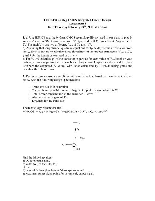
2. <strong>Design</strong> a common-source amplifier with a resistive load based on the schematic shown<br />
below with the following design specifications:<br />
Transistor M1 is in saturation<br />
The minimum possible output voltage to keep M1 in saturation is 0.2V<br />
Total power consumption of the amplifier is 3mW<br />
Absolute value of gain of 15<br />
L=0.5µm for the transistor<br />
The technology parameters are:<br />
λ(NMOS) = 0, γ = 0, VDD=3V, VTH(NMOS) = 0.5V, µnCox=1 mA/V 2<br />
Find the following values:<br />
a) DC level of the input,<br />
b) width (W1) of transistor M1,<br />
c) RD,<br />
d) nominal dc level (bias level) of the output node, and<br />
e) Maximum output signal swing for a symmetric output signal.
3. In the following circuit, assuming that the transistor is operating in the saturation<br />
region:<br />
a) Find the required Vbias for which the dc value of the Vout is 1.44V.<br />
b) Is the assumption that the transistor is in the saturation region correct?<br />
c) Find the small-signal gain Vout/Vsig.<br />
Assume λ = 0, γ = 1V 1/2 , 2ΦF=0.64V, VTH0= 0.4V, μnCox = 800 μA/V 2 , (W/L)NMOS = 20,<br />
RD = RS = 0.5kΩ, and VDD=1.8V.<br />
4. Calculate the gain of the following circuit at very low and very high frequencies.<br />
Neglect all other capacitances that are not shown in the circuit and assume λ = γ = 0.<br />
Good luck!