Wk2 - EECE 259 - Lab 1 - Using Multisim.pdf - Courses - University ...
Wk2 - EECE 259 - Lab 1 - Using Multisim.pdf - Courses - University ...
Wk2 - EECE 259 - Lab 1 - Using Multisim.pdf - Courses - University ...

You also want an ePaper? Increase the reach of your titles
YUMPU automatically turns print PDFs into web optimized ePapers that Google loves.
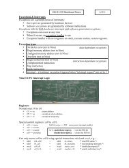
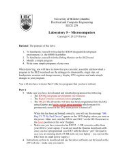
Rational: The purpose of this lab is :-<br />
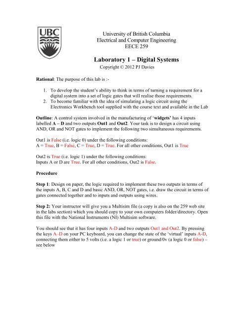
<strong>University</strong> of British Columbia<br />
Electrical and Computer Engineering<br />
<strong>EECE</strong> <strong>259</strong><br />
<strong>Lab</strong>oratory 1 – Digital Systems<br />
Copyright © 2012 PJ Davies<br />
1. To develop the student’s ability to think in terms of turning a requirement for a<br />
digital system into a set of logic gates that will realise those requirements.<br />
2. To become familiar with the idea of simulating a logic circuit using the<br />
Electronics Workbench tool supplied with the course text and available in the <strong>Lab</strong><br />
Outline: A control system involved in the manufacturing of ‘widgets’ has 4 inputs<br />
labelled A – D and two outputs Out1 and Out2. Your task is to design a circuit using<br />
AND, OR and NOT gates to implement the following two simultaneous requirements.<br />
Out1 is False (i.e. logic 0) under the following conditions:<br />
A = True, B = False, C = True, D = True. For all other conditions, Out1 is True<br />
Out2 is True (i.e. logic 1) under the following conditions:<br />
Inputs A or D are True. For all other conditions, Out2 is False.<br />
Procedure<br />
Step 1: Design on paper, the logic required to implement these two outputs in terms of<br />
the inputs A, B, C and D and basic AND, OR, NOT gates, i.e. draw the circuit in terms of<br />
gates connected together and to inputs and outputs using wires.<br />
Step 2: Your instructor will give you a <strong>Multisim</strong> file (a copy is also on the <strong>259</strong> web site<br />
in the labs section) which you should copy to your own computers folder/directory. Open<br />
this file with the National Instruments (NI) <strong>Multisim</strong> software.<br />
You should see that it has four inputs A-D and two outputs Out1 and Out2. By pressing<br />
the keys A–D on your PC keyboard, you can change the state of the ‘virtual’ inputs A-D,<br />
connecting them either to 5 volts (i.e. a logic 1 or true) or ground/0v (a logic 0 or false) –<br />
see below
Step3: <strong>Using</strong> the ‘place->component’ menu in NI <strong>Multisim</strong> software, chose components<br />
from TTL Group / 74LSxx series of devices and place them onto your circuit – see<br />
below. (Hint: the 74LS04N component contains 6 NOT gates, the 74LS08N contains 4,<br />
two input AND gates and the 74LS32N contains 4, two input OR gates).
Step 4: Start the simulation by clicking on the simulation switch<br />
Check your design gives the correct results (i.e. it meets the specification of the problems<br />
defined earlier in the ‘Outline’ by toggling the switches and observing the output lamps.<br />
Step 5: Stop your simulation (otherwise it will use huge PC resources if it runs for a long<br />
time). Now redesign your logic, to use ONLY a combination of NOT gates plus NAND<br />
gates (a Nand gate is an And gate with an inverter wired to the output – the 74LS00N<br />
component contains 4, two input Nand gates). Change your circuit within NI <strong>Multisim</strong><br />
and verify that the requirements are still met. Note you will have to think about how to<br />
create an OR gate from a NAND plus NOT gates (the theory was covered in lecture 1)<br />
7404 – Hex Inverters 7432 – Quad 2 input OR
7408 – Quad 2 input AND 7411 – Triple 3 input AND 7421 – Dual 4 input And<br />
7400 – Quad 2 input NAND 7410 – Triple 3 input NAND<br />
7402 – Quad 2 input NOR 7427 – Triple 3 input NOR