X-ray Photoelectron Spectroscopy of CdSe Nanocrystals - American ...
X-ray Photoelectron Spectroscopy of CdSe Nanocrystals - American ...
X-ray Photoelectron Spectroscopy of CdSe Nanocrystals - American ...

You also want an ePaper? Increase the reach of your titles
YUMPU automatically turns print PDFs into web optimized ePapers that Google loves.
J. Phys. Chem. 1994,98, 4109-41 17<br />
X-<strong>ray</strong> <strong>Photoelectron</strong> <strong>Spectroscopy</strong> <strong>of</strong> <strong>CdSe</strong> <strong>Nanocrystals</strong> with Applications to Studies <strong>of</strong> the<br />
Nanocrystal Sllrface<br />
Introduction<br />
J. E. Bowen Katari, V. L. Colvin, and A. P. Alivisatos'<br />
Materials Science Divisioh, Lawrence Berkeley Laboratory and Department <strong>of</strong> Chemistry,<br />
University <strong>of</strong> California, Berkeley, California 94720<br />
Received: December 13, 1993; In Final Form: February 10, 1994"<br />
4109<br />
We report the use <strong>of</strong> X-<strong>ray</strong> photoelectron spectroscopy (XPS) to determine the surface composition <strong>of</strong><br />
semiconductor nanocrystals. Crystalline, nearly monodisperse <strong>CdSe</strong> nanocrystals ranging in radius from 9 to<br />
30 A were chemically,synthesized and covalently bound to Au and Si surfaces for study. XPS core level peak<br />
positions for Cd and Se were in agreement with those <strong>of</strong> bulk <strong>CdSe</strong>. We have determined that the majority<br />
<strong>of</strong> Se atoms on the surface are unbonded as prepared and that Cd atoms are bonded to the surface ligand,<br />
tri-n-octylphosphine oxide, to the extent that such bonding is sterically allowed. We have determined that the<br />
total ligand saturation <strong>of</strong> the nanocrystal surface varies from 60% in the smaller nanocrystals to 30% in the<br />
larger nanocrystals. In addition, we have determined that upon exposure <strong>of</strong> the nanocrystals to air Se surface<br />
sites are oxidized, forming a SeOz surface film which causes the nanocrystals to degrade over time. The<br />
nanocrystal surface can be modified by dispersing the crystals in pyridine. Nearly all <strong>of</strong> the P ligands are<br />
removed in this case, leaving behind primarily unsaturated Cd and Se surface atoms. In this case, both Cd<br />
and Se oxidize upon exposure to air.<br />
The surface <strong>of</strong> an inorganic nanocrystal plays an important<br />
role in determining its structural, thermodynamic, optical, and<br />
transport properties. Because <strong>of</strong> low symmetry and the absence<br />
<strong>of</strong> long-range order on the crystal surface, traditional probes <strong>of</strong><br />
surface structure are not applicable. Thus, more is known about<br />
the interior composition and symmetry <strong>of</strong> nanocrystals than about<br />
the surface. In this paper we present a study <strong>of</strong> the surface<br />
composition <strong>of</strong> <strong>CdSe</strong> nanocrystals, with particular attention to<br />
the organic groups which cap the nanocrystals and to surface<br />
compounds formed after the nanocrystals are synthesized. This<br />
is in contrast to an XPS and Auger experiment which studied the<br />
composition <strong>of</strong> semiconductor nanocrystals onto which a layer <strong>of</strong><br />
a different semiconductor had been grown.' In that work, the<br />
primary focus was on quantifying the relative amount <strong>of</strong> each<br />
type <strong>of</strong> semiconductor species and proving that a shell has actually<br />
been formed, rather than looking specifically at the outer surface<br />
layer.<br />
Two previous experiments on the organic surface capping groups<br />
on cadmium chalcogenide nanocrystal surfaces have been per-<br />
formed.*.' The first experiment used NMR to determine bonding<br />
geometry and surface coverage <strong>of</strong> thiophenol on CdS nanocrys-<br />
tals.2 The second used 31P NMR to study the surface coverage<br />
<strong>of</strong> tri-n-octylphosphine oxide (TOPO) and TOPSe on <strong>CdSe</strong><br />
nanocrystals.3 This more recent study determined the total<br />
coverage <strong>of</strong> P-containing ligands and determined the relative<br />
amount <strong>of</strong> TOPOvs TOPSeon the surface for 18-A nanocrystals.<br />
NMR is probably the most powerful probe available for study<br />
<strong>of</strong> the bonding geometry at the nanocrystal surface. However,<br />
it does not immediately provide a route to the full composition<br />
<strong>of</strong> the surface. X-<strong>ray</strong> photoelectron spectroscopy provides such<br />
a probe <strong>of</strong> composition.<br />
Recently, techniques were developed which allow the chemical<br />
binding <strong>of</strong> nanocrystals to Au and A1 surfaces.4 The binding<br />
moleculesituates the nanocrystals - 10 A from the metal surface,<br />
allowing for electron tunneling between the nanocrystals and the<br />
surfaces in order to avoid charging. In addition, the samples are<br />
supported on a macroscopic surface. This has allowed the<br />
exploration <strong>of</strong> the range <strong>of</strong> more traditional surface techniques<br />
* Abstract published in Advance ACS Abstracts, March 15, 1994.<br />
for use on nanocrystals. In this paper we report the use <strong>of</strong> a<br />
traditional surface science technique, XPS, to explore the surface<br />
properties <strong>of</strong> semiconductor nanocrystals. We have synthesized<br />
nearly monodisperse, crystalline <strong>CdSe</strong> nanocrystals for this study,<br />
using a variation <strong>of</strong> a technique developed by Mur<strong>ray</strong> et al.5 We<br />
have bound the nanocrystals to Au and Si surfaces. Finally, we<br />
have performed XPS on a variety <strong>of</strong> <strong>CdSe</strong> nanocrystal sizes and<br />
determined the types <strong>of</strong> surface species present as well as the<br />
percent coverage <strong>of</strong> these species.<br />
Experiment<br />
Synthesis. Mur<strong>ray</strong> et ale5 have recently reported a powerful<br />
new method for making crystalline, monodisperse, size-tunable<br />
<strong>CdSe</strong> nanocrystals. We have adapted their method, with some<br />
changes that are reported below. The principal difference between<br />
the preparations is the temperature <strong>of</strong> injection, which affects<br />
the time evolution <strong>of</strong> the nanocrystal growth as well as the<br />
crystallinity and shape <strong>of</strong> the nanocrystals. The nanocrystals<br />
produced by the method below are nearly monodisperse without<br />
size-selective precipitation, are crystalline, and are spherical.<br />
All <strong>of</strong> the following procedures are carried out using standard<br />
airless techniques. Dimethylcadmium was purchased from Strem<br />
Scientific and filtered prior to use. Se (60 mesh) powder, 99%<br />
tri-n-octylphosphine oxide (TOPO), tributylphosphine (TBP),<br />
and anhydrous methanol were used as received from Aldrich.<br />
Toluene (Aldrich) was distilled over sodium metal. Anhydrous<br />
pyridine was used as received from Burdick and Jackson.<br />
A typical preparation proceeds as follows. A 0.8-g sample <strong>of</strong><br />
Se is dissolved in 8.0 g <strong>of</strong> TBP, and 2.0 g <strong>of</strong> dimethylcadmium<br />
is then added. This solution is then diluted by 4:l with TBP, and<br />
the resulting solution is septa capped and removed from the drybox.<br />
Twelve grams <strong>of</strong> TOPO is heated to -350 OC under Ar.<br />
WARNING Heating should be done with extreme caution as<br />
350 'C is well above TOPO's flash point. Differences in<br />
temperature <strong>of</strong> less than 1 O C can change both the average size<br />
and the quality <strong>of</strong> the size distribution. When the temperature<br />
has stabilized, 0.4 mL <strong>of</strong> the MezCd/Se solution is added. The<br />
solution immediately changes color, indicating the formation <strong>of</strong><br />
nanocrystals. This solution is removed from the heat and allowed<br />
to cool. In order to prevent any oxidation <strong>of</strong> the nanocrystal<br />
surface, the solution is cooled to room temperature under Ar.<br />
0022-3654/94/2098-4109$04.50/0 0 1994 <strong>American</strong> Chemical Society
4110<br />
The Journal <strong>of</strong> Physical Chemistry, Vol. 98, No. 15, 1994 Katari et al.<br />
This solid solution is then transferred to the drybox where methanol<br />
is added, dissolving the TOP0 and precipitating the nanocrystals.<br />
This mixture is then filtered through a 0.1-pm filter, and the<br />
recovered powder <strong>of</strong> nanocrystals is stored under nitrogen. In<br />
practice, little oxidation is observed when the precipitation and<br />
filtration are done in air, as long as the resulting powder is stored<br />
under nitrogen. The resulting nanocrystals can be dispersed in<br />
toluene and can also be dispersed in pyridine. Simply dispersing<br />
the nanocrystals in pyridine, without significant washing, is<br />
sufficient to change their surface composition. Note that we<br />
have used TBP as the Se solvent rather than trioctylphosphine<br />
(TOP), which is used by Mur<strong>ray</strong> et al.5 We initially used TBP<br />
in order to achieve low coverage <strong>of</strong> the Se surface atoms, as the<br />
tributylphosphine will more readily be removed in the high-<br />
temperature conditions that we use. However, comparison <strong>of</strong><br />
our surface experiments with those <strong>of</strong> Becerra et al.) indicates<br />
that the surface characteristics <strong>of</strong> nanocrystals synthesized using<br />
TOP and TBP are rather similar.<br />
In order to make nanocrystals with absorption maxima larger<br />
than 580 nm, modifications<strong>of</strong> the above procedure are employed.<br />
One method is to cool the 350 OC solution to 320 "C and allow<br />
it to continue heating for several minutes. The size can be<br />
monitored by removing aliquots <strong>of</strong> the solution at time intervals.<br />
This does create larger nanocrystals; however, the initial size<br />
distribution is lost. A better way to increase the average size <strong>of</strong><br />
the nanocrystals is to add stock solution in 0.1-mL intervals to<br />
a 300 OC solution over a period <strong>of</strong> several minutes. This technique<br />
allows for better retention <strong>of</strong> the initial size distribution than the<br />
pure heating method.<br />
Characterization <strong>of</strong> <strong>Nanocrystals</strong>. Absorption spectra were<br />
obtained using an HP Model 8452 ultraviolet-visible absorption<br />
(UV-vis) diode ar<strong>ray</strong> spectrometer with a collimated deuterium<br />
lamp source. The resolution is 2 nm. Samples were dispersed<br />
in toluene or pyridine for measurement. These solvents limit the<br />
useful lower limit <strong>of</strong> the spectrometer to -320 nm.<br />
Representative samples were characterized by X-<strong>ray</strong> powder<br />
diffraction using a Siemens Model D5000 X-<strong>ray</strong> diffractometer<br />
with Cu Ka radiation. <strong>CdSe</strong> powders were placed on glass plates<br />
for measurement or were pressed onto Ta foils. The diffraction<br />
from most metal foils interferes with the <strong>CdSe</strong> pattern. However,<br />
Ta's crystal structure is such that it does not interfere. Domain<br />
sizes <strong>of</strong> nanocrystals were obtained by fitting the width <strong>of</strong> the<br />
peaks and translating this to domain sizes using standard formulas<br />
for spherical nanocrystah6<br />
Fourier transform infrared spectroscopy was performed using<br />
a Nicolet FTIR spectrometer. Powdered nanocrystal samples<br />
were mixed with KBr. The resulting powder was finely ground<br />
and pressed into a optically clear pellet using a hydraulic press.<br />
Spectra were collected over the range from 400 to 4000 cm-l.<br />
Sizing. Sizes <strong>of</strong> the nanocrystals were obtained by comparing<br />
optical absorption spectra <strong>of</strong> all samples to spectra from a large<br />
number <strong>of</strong> samples sized using transmission electron microscopy<br />
(TEM) and small-angle X-<strong>ray</strong> scattering (SAXS).'<br />
Binding <strong>Nanocrystals</strong> to Surfaces. In order to perform<br />
photoelectron spectroscopy on the nanocrystals, the nanocrystals<br />
must first be attached to a conducting surface so that they will<br />
not charge during performance <strong>of</strong> the experiment. Several things<br />
are important for this attachment. First, the nanocrystals must<br />
be positioned a uniform distance from the conducting surface,<br />
and thisdistance must bevery small. In addition, thenanocrystals<br />
must be in a single layer, with no nanocrystals sitting on top <strong>of</strong><br />
other nanocrystals. Finally, the samples must be robust to<br />
facilitate transfer between different experiments. These three<br />
requirements are best satisfied by chemically binding the<br />
nanocrystals to the surface. Most <strong>of</strong> the samples used in this<br />
study were bound to gold surfaces using techniques described<br />
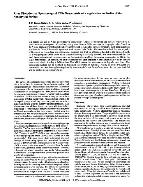
elsewhere.4 Briefly, hexanedithiol is allowed to self-assemble on<br />
ion-etched gold evaporated onto glass slides. The slides are then<br />
transferred to a solution <strong>of</strong> nanocrystals, which covalently bond<br />
to the sulfur <strong>of</strong> the hexanedithiol (Figure 1). Empirically, we<br />
Toluene<br />
solution<br />
*$k' d<br />
>i!@:L< %Ju<br />
Gold surface<br />
Figure 1. Attachment <strong>of</strong> <strong>CdSe</strong> nanocrystals dissolved in toluene to Au<br />
surfaces with hexanedithiol.<br />
have found that hexanedithiol maximizes the nanocrystal coverage<br />
relative to longer and shorter chain dithiols. We believe that the<br />
longer chains can loop, forming two linkages to gold, while the<br />
shorter chains do not bind strongly enough to the gold to strongly<br />
bind the nanocrystals to the surface. Hexanedithiol most likely<br />
does not form an ordered monolayer, because <strong>of</strong> its length.8<br />
However, it is possible to use a more complex method <strong>of</strong> binding,<br />
modeled after a method used on trichlorosilanes by Wasserman<br />
et al.,9 which should yield an ordered organic substrate to which<br />
to bind the nanocrystals. In this scheme, a long-chain alkanethiol<br />
with a terminating thioacetate group would be bound to the Au.<br />
After assembly, the thioacetate group could be converted to a<br />
thiol and exposed to the nanocrystals.<br />
We have also bound nanocrystals to doped Si surfaces. p-doped<br />
Si( 1 11) wafers were first cleaned by immersion in a 1: 1 solution<br />
<strong>of</strong> methanol (Aldrich) and 45% hydrochloric acid (Aldrich),<br />
followed by immersion in concentrated sulfuric acid (Aldrich).lo<br />
The wafers were then rinsed with distilled water. The technique<br />
used to bind the nanocrystals to the cleaned and oxidized Si surface<br />
follows a technique used to bind Au coats to glass slides." The<br />
wafers were placed in a boiling solution <strong>of</strong> 10 g <strong>of</strong> distilled water<br />
and 10 g <strong>of</strong> (3-mercaptopropy1)trimethoxysilane (MPS) (Sigma)<br />
in 400 g <strong>of</strong> 2-propanol (electronic grade, Aldrich). After 10 min,<br />
the wafers were removed, rinsed in 2-propanol, dried with Ar,<br />
and placed in a 100 OC oven. This was repeated three times. The<br />
wafers were then placed in a solution <strong>of</strong> <strong>CdSe</strong> nanocrystals and<br />
allowed to sit overnight. The wafers were then removed from<br />
solution and rinsed with the nanocrystals' solvent, dried with<br />
nitrogen, and stored. Note that for both techniques the MPS or<br />
hexanedithiol coated surfaces could be pumped into the glovebox,<br />
where the particle solution could be added without exposure to<br />
air. In practice, this was not necessary to avoid oxidation as long<br />
as the finished samples were stored under nitrogen.<br />
Characterization on Surfaces. Resonance Raman spectroscopy<br />
was performed on the nanocrystals using a setup described<br />
previously.12 Briefly, an Ar-ion pumped dye laser is used to excite<br />
the nanocrystals on resonance. The Raman scattering is then<br />
detected <strong>of</strong>f axis using a double monochromator with output fed<br />
to a CCD camera. The samples were cooled to 77 K or lower<br />
under vacuum for the measurement, in order to allow accurate<br />
comparison with more traditional Raman experiments, which<br />
are done on polymer films at these temperatures.<br />
Rutherford backscattering spectroscopy (RBS) provides a<br />
measure <strong>of</strong> the absolute number <strong>of</strong> atoms <strong>of</strong> each element per<br />
square centimeter on the samplesurfaces, which can be translated<br />
to percent monolayer coverage. RBS was performed at the RBS<br />
facility <strong>of</strong> the Materials Science Division <strong>of</strong> Lawrence Berkeley<br />
Laboratory.
XPS <strong>of</strong> <strong>CdSe</strong> <strong>Nanocrystals</strong> The Journal <strong>of</strong> Physical Chemistry, Vol. 98, No. 15, 1994 4111<br />
1 Bulk Band Gap , ')<br />
1.5 2.0 2.5 3.0 3.5<br />
Energy (eV)<br />
Figure 2. UV-vis absorption spectra <strong>of</strong> <strong>CdSe</strong> nanocrystals: (a) r = 9.3<br />
A; (b) r = 10.0 A; (c) r = 10.4 A; (d) r = 10.7 A; (e) r = 11.4 A; (f)<br />
r = 12.3 A; (g) r = 13.2 A; (h) r = 14.1 A; (i) r = 15.9 A; (j) r = 18.0<br />
A; (k) r = 24.2 A; (1) r = 33.5 A.<br />
XPS was performed using a Perkin-Elmer PHI 5300 ESCA<br />
System machine located in the Materials Science Division <strong>of</strong><br />
Lawrence Berkeley Laboratory. Both Mg and A1 anodes driven<br />
at 400 W were used for this study. All scans were obtained using<br />
the 1-cm2 aperture. Survey scans were collected over the range<br />
from 1100 to 0 eV with 179-eV pass energy detection, corre-<br />
sponding to a resolution <strong>of</strong> 4.5 eV. Typical surveys were collected<br />
for 5 min. Close-up scans were collected over a range <strong>of</strong> 20 eV<br />
around the peak <strong>of</strong> interest with either 8.9-eV pass energy detection<br />
or 35.7-eV pass energy detection, which correspond to 0.69- and<br />
1 .l-eV resolution, respectively, with the Mg anode. Typical close-<br />
up scans were detected for 10-20 min per element. Measurements<br />
were performed at pressures lower than 1 X 10⁻⁸ Torr. All spectra<br />
were calibrated using the position <strong>of</strong> the Au 4f peaks present in<br />
all spectra as a standard.<br />
Results<br />
Characterization <strong>of</strong> Samples. All samples were characterized<br />
using UV-vis. Spectra (Figure 2) indicate nearly monodisperse<br />
nanocrystals with a range in exciton peak position from 1.9 to 2.5<br />
eV. The room temperature bulk band gap for wurtzite <strong>CdSe</strong> is<br />
1.74 eV.l3<br />
X-<strong>ray</strong> diffraction patterns on a large number <strong>of</strong> samples indicate<br />
wurtzite nan~rystals.1~ The domain sizes for the large majority<br />
<strong>of</strong> nanocrystals agreed with the sizing obtained by direct means,<br />
indicating good crystallinity <strong>of</strong> the nanocrystals. In addition, the<br />
shape <strong>of</strong> the spectra indicate spherical particles with few or no<br />
stacking faults, based on comparison to the calculated spectra <strong>of</strong><br />
Mur<strong>ray</strong> et al.5J4<br />
TEM images <strong>of</strong> nanocrystals indicated good crystallinity <strong>of</strong><br />
the nanocrystals and a spherical shape (Figure 3), justifying the<br />
straightforward treatment <strong>of</strong> the X-<strong>ray</strong> diffraction data. Sizes<br />
and distributions obtained from SAXS generally agreed with the<br />
TEM measurements, with the sizes from SAXS generally larger,<br />
because <strong>of</strong> the greater sensitivity to the disordered surface <strong>of</strong><br />
SAXS.' The curve used to size the nanocrystals is shown in<br />
Figure 4.<br />
FTIR was used as a probe <strong>of</strong> the presence <strong>of</strong> TOPO on the<br />
nanocrystal surface. The nanocrystal spectrum had peaks<br />
matching all <strong>of</strong> the TOPO peaks in frequency and relative<br />
intensity, except for the P-0 stretch, which was shifted lower by<br />
-20 cm-l relative to bulk TOPO (Figure 5). This is in agreement<br />
with IR measurements performed on triphenylphosphine oxides<br />
,<br />
Figure 3. Transmission electron micrograph <strong>of</strong> <strong>CdSe</strong> nanocrystals.<br />
s v<br />
2.6 -<br />
2.4 -<br />
.-<br />
c<br />
u)<br />
n<br />
y 2.2 -<br />
(D<br />
n<br />
C<br />
2 2.0 -<br />
.-<br />
0<br />
w<br />
8<br />
a*<br />
J&T<br />
VO<br />
T<br />
.o<br />
0<br />
O T<br />
O T<br />
0<br />
T<br />
TEM<br />
SAXS<br />
T o<br />
i 5 10 15 20 25 30 35 40 45 50<br />
Radius (A)<br />
Figure 4. Exciton peak position from UV-vis vs measured radius from<br />
TEM and SAXS.<br />
ls00 lib0 do0 1000<br />
Frequency (cm-1)<br />
Figure 5. FTIR spectra: (a) TOPO dispersed in KBr; (b) <strong>CdSe</strong><br />
nanocrystals dispersed in KBr.<br />
complexing to CdI2 and other metal salts,lS which typically show<br />
shifts in P-0 frequency <strong>of</strong> between 20 and 60 cm-1 upon<br />
complexation.<br />
Raman spectroscopy (Figure 6) was used to confirm the<br />
presence <strong>of</strong> nanocrystals on the surface. Use <strong>of</strong> the Si substrate<br />
provides the built-in standard <strong>of</strong> the Si TO mode at 522 cm-I.<br />
All samples show the presence <strong>of</strong> the <strong>CdSe</strong> LO mode at 212 cm-l<br />
as well as the first and second overtone. The presence <strong>of</strong> the<br />
surface quenches part <strong>of</strong> the fluorescence, allowing for greater<br />
ease <strong>of</strong> measurement <strong>of</strong> the spectrum <strong>of</strong> samples bound to surfaces<br />
than <strong>of</strong> samples in polymers or as powder. The Raman line width
4112 The Journal <strong>of</strong> Physical Chemistry, Vol. 98, No. 15, 1994 Katari et al.<br />
2000 1 7<br />
I I<br />
200 300 400 500<br />
Frequency (cm-’)<br />
Figure 6. (a) Raman spectrum <strong>of</strong> <strong>CdSe</strong> nanocrystals bound to Si, taken<br />
at 77 K. r = 9.3 A. (b, c) Raman spectra <strong>of</strong> <strong>CdSe</strong> nanocrystals bound<br />
to gold, taken at 16 K: (b) r = 11.4 A; (c) r = 18.0 A. Note that<br />
fluorescence has been quenched by the presence <strong>of</strong> the surfaces.<br />
for the nanocrystals varies with size in the same way as in previous<br />
studies on CdS.12J6<br />
RBS measurements indicate coverage <strong>of</strong> -1015 Cd and Se<br />
atoms per cm2, which corresponds to -1/6 <strong>of</strong> a monolayer <strong>of</strong><br />
nanocrystals on the Si surface. The signal from the Au in RBS<br />
prevents use <strong>of</strong> the technique for gold substrate samples. However,<br />
comparison <strong>of</strong> the XPS signals from both types <strong>of</strong> samples indicates<br />
that coverage does not differ significantly between the two types<br />
<strong>of</strong> samples.<br />
Together, these techniques indicate that nearly monodisperse<br />
and highly crystalline <strong>CdSe</strong> nanocrystals <strong>of</strong> wurtzite structure<br />
are present in - 1 /6 monolayer coverage on Au and Si substrates.<br />
Because <strong>CdSe</strong> fails to show up in samples in which the<br />
hexanedithiol or MPS is not applied, these techniques also indicate<br />
that the samples are bound to the surfaces by the hexanedithiol<br />
or MPS. However, the degree <strong>of</strong> order <strong>of</strong> the dithiol and MPS<br />
is not assessed by these techniques and is expected to be low.<br />
Determination <strong>of</strong> Composition from <strong>Photoelectron</strong> Spectra. In<br />
order to use an observed photoelectron spectrum to derive<br />
composition information, several factors must be accounted for.<br />
This is well described in Wagner et al.’s XPS handb0ok.1~ In<br />
summary, the intensity <strong>of</strong> a peak (the relative number <strong>of</strong> electrons<br />
detected) in XPS from a single element for a homogeneous sample<br />
is<br />
where n is the number <strong>of</strong> atoms per cm3, f is the X-<strong>ray</strong> flux, Q<br />
is the cross section for the photoelectric process, 0 is an angular<br />
factor, y is the efficiency for formation <strong>of</strong> photoelectrons with the<br />
full kinetic energy, A is the escape depth <strong>of</strong> photoelectrons <strong>of</strong> that<br />
kinetic energy, A is the area <strong>of</strong> the sample being probed, and T<br />
is a factor for the efficiency <strong>of</strong> detecting electrons <strong>of</strong> a given<br />
kinetic energy. Inverting eq 1, we determine that<br />
Typically, the entire denominator is bundled and called S, the<br />
atomic sensitivity factor. Values for this factor have been<br />
experimentally determined and theoretically calculated for a<br />
variety <strong>of</strong> different types <strong>of</strong> XPS systems.lS The numeric value<br />
will vary from system to system because the transmission factor<br />
will vary between different electron detection systems. In order<br />
to determine relative concentrations <strong>of</strong> atoms in a homogeneous<br />
system, one simply divides each atom’s peak intensity by its<br />
sensitivity factor and takes the ratio.<br />
In a nanocrysal sample, as in other types <strong>of</strong> heterogeneous<br />
systems, this straightforward analysis is not adequate because<br />
900<br />
Cd 3d 1<br />
800 I<br />
p 500 .<br />
450<br />
400<br />
p 250 -<br />
c Is<br />
I<br />
E 200 -<br />
X<br />
150 - Cd 4d<br />
Au 4p<br />
Au 4f<br />
Cd3p Cd Auger<br />
50<br />
01<br />
l<br />
I<br />
-50 0 50 100 150 200 250 300<br />
Binding Energy (eV)<br />
Figure 7. Typical XPS survey spectra <strong>of</strong> <strong>CdSe</strong> nanocrystals bound to<br />
gold using Mg X-<strong>ray</strong> source.<br />
the equation assumes a homogeneous, thick (>200 nm) sample.<br />
This is manifested in the inclusion <strong>of</strong> X as the factor for the escape<br />
depth. The appropriate way to account for the escape depth is<br />
to integrate over the entire region <strong>of</strong> interest, modifying the<br />
intensity from each point by an exponential factor which decreases<br />
with depth away from the surface.1g Thus, for a flat homogeneous<br />
sample, the appropriate integral is just<br />
Jde-’/’ dz (3)<br />
where d is the depth <strong>of</strong> the sample. Escape depths are in the<br />
range from 4 to 20 A, so for d > 20 nm the integral is just equal<br />
to A. However, in nanocrystals, the depth <strong>of</strong> the sample is <strong>of</strong> the<br />
same order <strong>of</strong> magnitude as the escape depth, and so the above<br />
equation willnot hold. Now wemust integrate theaboveequation<br />
over a sphere, with z modified to be the distance from a point<br />
within a sphere to the sphere’s surface in the direction <strong>of</strong> the<br />
analyzer. Thus, in the calculation <strong>of</strong> the compositional ratios,<br />
the calculated sensitivity factors are divided by X and then<br />
multipled by the appropriate integral, and then the two factors<br />
are ratioed. Escape depths are - 15 %, for the Cd 3d cores, -20<br />
A for the P 2p cores, and -21 %I for the Se 3d cores for Mg KCY<br />
radiation. In the end, the ratio <strong>of</strong> the two integrals is much closer<br />
to unity than the ratio <strong>of</strong> the two escape depths, because the<br />
nanocrystals are about the same size as the escape depths. The<br />
corrections performed in this way will alter the composition by<br />
as much as 30% in the smaller nanocrystals. This effect only<br />
becomes negligible (< 1 % difference) for diameters greater than<br />
-90 A.<br />
Multiple XPS measurements have been taken on 22 different<br />
preparations <strong>of</strong> <strong>CdSe</strong> nanocrystals ranging in radius from 9.3 to<br />
30.2 A. Typical survey spectra (Figure 7) were obtained in 5 min<br />
using 178-eV pass energy. They show the presence <strong>of</strong> Au from<br />
the substrate, Cd, Se, and P from the nanocrystals and their<br />
surfaces, and C and 0 from the nanocrystals’ surfaces and from<br />
absorbed gaseous molecules. The survey spectra give a rough<br />
idea <strong>of</strong> the coverage <strong>of</strong> nanocrystals on the surface-when the<br />
Cd 3d signal is larger than that from Au 4f, the coverage is<br />
comparable to Si substrate samples which had coverages <strong>of</strong> - 1 /6<br />
monolayer.<br />
Higher-resolution spectra were taken <strong>of</strong> the Cd and Se regions<br />
<strong>of</strong> samples as prepared (Figure 8). The scans showed no evidence
XPS <strong>of</strong> <strong>CdSe</strong> <strong>Nanocrystals</strong><br />
100 I 1 100 I I<br />
80 I<br />
r\<br />
Cd 3d5/2<br />
Cd3d3’2 ~<br />
I 80 A<br />
Se 3d<br />
400 405 410 415 420 50 55 60 65 70<br />
Binding Energy (eV) Binding Energy (eV)<br />
Figure8. Close-up surveys for Cd 3d and Se 3d cores. Signals have been<br />
<strong>of</strong>fset relative to each other for clarity. (a, b) r = 10.0 A; (c, d) r = 15.9<br />
A; (e, f) r = 12.3 A.<br />
<strong>of</strong> peaks other than the Cd and Se cores from the main and<br />
satellite Mg X-<strong>ray</strong>s, and the satellite peaks <strong>of</strong> Au, in the Se case.<br />
There was no evidence <strong>of</strong> shake-up peaks, which are photoemission<br />
peaks from species ionized prior to the observed photoemission<br />
process and generally occur several electronvolts to higher binding<br />
energy <strong>of</strong> the main peak in the spectra. Cd 3d5/2 peak positions<br />
ranged from 405.1 to406.0eV, with a normal distribution centered<br />
around 405.6 f 0.2 eV. Se 3d peak positions ranged from 54.3<br />
to 54.9 eV, with a normal distribution centered around 54.6 f<br />
0.2 eV. The Cd and Se peak positions moved together, so that<br />
the difference between the two peak positions averaged 351.0 f<br />
0.1 eV. In bulk <strong>CdSe</strong>, this difference is 350.97.20 Note that<br />
comparison <strong>of</strong> absolute positions is meaningless because the bulk<br />
studies are referenced to the valence band edge <strong>of</strong> <strong>CdSe</strong>, which<br />
we cannot see in our spectra due to the interference from the Au<br />
valence band. In addition, we would expect the valence band<br />
edge <strong>of</strong> our material to shift as a function <strong>of</strong> size, as in CdS,21<br />
which also prevents comparison.<br />
Peak areas <strong>of</strong> the Cd and Se cores were measured and used<br />
to calculate Cd to Se ratios for the nanocrystals as described<br />
above. Areas were determined by fitting each <strong>of</strong> the curves using<br />
a nonlinear least-squares curve-fitting programZ2 and taking the<br />
area <strong>of</strong> the fit peak. The absolute areas are only accurate to an<br />
error <strong>of</strong> -lo%, because <strong>of</strong> the uncertainty in the precise shape<br />
<strong>of</strong> the background. However, the background is kept the same<br />
for all fits, and so the relative error is much smaller-the typical<br />
error in fits was 1-2%. An empirical correction was made for<br />
the pass energy variation between the two scans when there was<br />
a difference. The calculated Cd:Se ratio was 1.02 f 0.14 and<br />
did not vary systematically with size. This average ratio is in<br />
agreement with elemental analysis <strong>of</strong> the powder samples.<br />
Deviations <strong>of</strong> composition measured by XPS from that determined<br />
by independent elemental analysis would indicate orientation <strong>of</strong><br />
faceted nanocrystals upon binding to the gold surface. We have<br />
seen no evidence <strong>of</strong> this occurring.<br />
Surface Properties <strong>of</strong> <strong>Nanocrystals</strong> Deposited from Toluene.<br />
High-resolution scans <strong>of</strong> the P region <strong>of</strong> the nanocrystals deposited<br />
from toluene solution provide information about the surface <strong>of</strong><br />
the nanocrystals. The P peak position is 133.7 f 0.3. This peak<br />
position is -1.5 eV higher than the peak position for tertiary<br />
phosphine oxides, sulfides,” and, by analogy, selenides. However,<br />
the IR shift <strong>of</strong> the P-0 frequency to lower energy upon<br />
complexation indicates a transfer <strong>of</strong> electron density from P to<br />
the 0, causing the P to be more positive when complexed to Cd15<br />
and hence have larger binding energy. Experiments on P-metal<br />
bonds have been limited to studies <strong>of</strong> covalent bonds;17 however,<br />
an estimate <strong>of</strong> the binding energy <strong>of</strong> P in a tertiary phosphine<br />
datively bound to Cd can be made as follows. The binding energy<br />
<strong>of</strong> phosphorus in a tertiary phosphine is 129 eV.17 The binding<br />
energy <strong>of</strong> P in a tertiary phosphine oxide is 132 eV.I7 Relative<br />
to the tertiary phosphine, P will be more positive when bound to<br />
Cd, as it will donate electrons to Cd, and thus its binding energy<br />
The Journal <strong>of</strong> Physical Chemistry, Vol. 98, No. 15, 1994 4113<br />
P-metal P-0<br />
400 41 0 420 130 140<br />
Binding Energy (eV) Binding Energy (eV)<br />
Figure 9. Close-up surveys for Cd 3d and P 2p cores. Signals have been<br />
corrected for the relative sensitivity factors. (a, b) r = 10.0 A; (c, d) r<br />
= 15.9 A. Note that the P/Cd ratio is smaller for the larger size.<br />
TABLE 1<br />
radius P/Cd radius P/Cd radius P/Cd<br />
(A) ratio (A) ratio (A) ratio<br />
9.3 0.77 10.4 0.56 13.1 0.36<br />
9.6 0.69 10.7 0.53 13.2 0.47<br />
9.6 0.66 11.4 0.56 13.2 0.44<br />
10.0 0.73 11.4 0.46 13.2 0.46<br />
10.0 0.74 11.4 0.41 15.9 0.42<br />
10.0 0.72 11.4 0.49 17.8 0.21<br />
10.0 0.68 11.7 0.46 19.9 0.24<br />
10.0 0.82 12.3 0.47 22.1 0.22<br />
10.4 0.61 12.3 0.40 30.2 0.21<br />
will be larger. Relative to a tertiary phosphine oxide, P will be<br />
less positive when bound to Cd, as it will not donate as much<br />
electron density to the Cd as it would to the oxide, and thus its<br />
binding energy will be less. Combining these two effects, we get<br />
an estimate <strong>of</strong> the binding energy <strong>of</strong> P in a tertiary phosphine<br />
bound to cadmium <strong>of</strong> ~ 1 3eV. 1 Thus, it is unlikely that the<br />
measured P peak corresponds to P directly datively bound to Cd.<br />
The technique used to calculate Cd:Se ratios can also be used<br />
to determine the surface coverage <strong>of</strong> ligands on the surface <strong>of</strong> the<br />
nanocrystals by comparing the Cd and P peaks with the<br />
modification <strong>of</strong> eq 3 so that the P integral is over a spherical shell<br />
rather than over the full sphere (Figure 9). Note that, for a<br />
nanocrystal <strong>of</strong> radius 25 A, the signal from P atoms on the surface<br />
<strong>of</strong> the nanocrystal facing the analyzer will contribute 10 times<br />
as much signal as P atoms on the surface <strong>of</strong> the nanocrystal<br />
facing away from the analyzer, so this mbdification is essential.<br />
Peak areas <strong>of</strong> the Cd and P peaks are then calculated and ratioed<br />
as above (Table 1). Only those samples which were dispersed in<br />
toluene are included here. Those dispersed in pyridine showed<br />
little P content. The Cd/P ratios fit best to a 1 /r curve, indicating<br />
that the ligands are indeed on the surface. The absolute error<br />
in this measurement comes primarily from the uncertainty with<br />
which the background is fit, as in the Cd:Se ratio measurement.<br />
However, the background is modeled in the same way across all<br />
samples, so that the relative error is much smaller. Thus, trends<br />
with size are meaningful. An additional error in this measurement<br />
comes from our sample preparation. The dithiols which bind the<br />
nanocrystals to the Au surface will necessarily displace ligands<br />
from Cd surface atoms. However, we believe that this is a minor<br />
effect on our measurements <strong>of</strong> surface coverage because <strong>of</strong> the<br />
limited area <strong>of</strong> the nanocrystal surface which the dithiols are able<br />
to reach given their maximum and minimum extension. Note<br />
that this effect will cause us to slightly underestimate the total<br />
coverage on the surface and will become less significant as the<br />
nanocrystal size increases.
4114 The Journal <strong>of</strong> Physical Chemistry, Vol. 98, No. 15, 1994<br />
100,<br />
0 Data<br />
Closest packing<br />
-<br />
70 0 <strong>of</strong> TOPO cones 1<br />
O<br />
. .<br />
I.. . natari et ai.<br />
ae<br />
------+<br />
30 -<br />
20 -<br />
400 405 410 415 420 125 130 135 140 145 150<br />
Binding Energy (eV)<br />
Binding Energy (eV)<br />
lo 0 4 Figure 12. Cd and P cores for oxidized cluster <strong>of</strong> Figure 10: (a) Cd 3d<br />
5 10 15 20 25 30 35<br />
cores; (b) P 2p cores. Note that the Cd and P cores do not change<br />
Radius (A)<br />
substantially.<br />
Figure 10. Percent coverage <strong>of</strong> P-containing ligands (primarily TOPO)<br />
on the cluster surface vs radius. Graph shows data as measured by XPS<br />
along with a calculation based on steric considerations (see text).<br />
22000<br />
20000 SeO2<br />
14000<br />
12000 i<br />
<strong>CdSe</strong><br />
J<br />
.. :=.<br />
SeOp<br />
I<br />
6000<br />
50 55 60<br />
Binding Energy (eV)<br />
65 70<br />
Figure 11. Oxidation<strong>of</strong>the<strong>CdSe</strong>surfaceSe3dcores: (a) 13.1-Acluster<br />
as prepared with no air exposure; (b) 13.1-,& cluster after air exposure<br />
for 24 h.<br />
A percent coverage <strong>of</strong> ligands on the surface was obtained by<br />
first calculating the number <strong>of</strong> <strong>CdSe</strong> units in a nanocrystal <strong>of</strong> the<br />
given radius, using the bulk density, which does not change<br />
significantly with size.23 Then, the number <strong>of</strong> <strong>CdSe</strong> units in a<br />
nanocrystal <strong>of</strong> the given radius minus the <strong>CdSe</strong> bond length <strong>of</strong><br />
2.63 AZ3 was calculated, and this number was subtracted from<br />
the previous number, giving the number <strong>of</strong> Cd and Se units on<br />
the surface. Then the percent coverage is obtained by taking the<br />
PCd ratio and multiplying it by the total number <strong>of</strong> Cd atoms<br />
on the surface <strong>of</strong> the nanocrystal and dividing this number by the<br />
total number <strong>of</strong> Cd and Se surface atoms per nanocrystal. Thus,<br />
assuming a uniform distribution <strong>of</strong> Cd and Se on the nanocrystal<br />
surface, a 50% coverage means that every Cd atom is bound to<br />
one TOPO molecule on average, with nothing bound to the surface<br />
Se atoms. The percent coverage is larger for smaller size<br />
nanocrystals and varies from 60% to 30% (Figure 10). This is<br />
in agreement with the work <strong>of</strong> Becerra et al., which showed 55%<br />
coverage on an 18-&radius nanocrystal.3<br />
Further information on the surface <strong>of</strong> nanocrystals may be<br />
obtained by studying the Cd and Se peaks over time in air. All<br />
samples developed an oxidized Se peak after spending time in air<br />
(Figure 11). The typical time for appearance <strong>of</strong> the peak was<br />
1 day. The peak's position relative to the <strong>CdSe</strong> peak agrees with<br />
the peak position seen for Se oxides on bulk <strong>CdSe</strong>, as would be<br />
expected.24 No similar oxidation <strong>of</strong> the Cd peak was observed<br />
(Figure 12a). In addition, upon oxidation <strong>of</strong> the Se, little decay<br />
in the P signal is observed (Figure 12b): over 1 week, the P signal<br />
decreased by less than 10%.<br />
The temporal behavior <strong>of</strong> the peak is somewhat surprising.<br />
After the initial rise <strong>of</strong> the oxide peak, the peak slowly decays<br />
and then rises again (Figure 13). Oscillations continue over the<br />
period <strong>of</strong> several weeks, perhaps longer. During the time that the<br />
oxidized peak is decaying, the Cd:Se ratio is rising, indicating the<br />
loss <strong>of</strong> Se from the nanocrystal.<br />
52 54 56 58 60 62<br />
Binding Energy (eV)<br />
Figure 13. Oxidation<strong>of</strong>the<strong>CdSe</strong>surface-Se 3dcores: (a) 13.1-,&cluster<br />
as prepared; (b-f') cluster after 24, 48, 72, 96, and 120 h in air. Note<br />
decay <strong>of</strong> oxide peak followed by reemergence in (f).<br />
I Au 41 1, I<br />
-50 0 50 100 150 200 250 300<br />
Binding Energy (eV)<br />
1 Au 4fI Se<br />
-50 0 50 100 150 200 250 300<br />
Binding Energy (eV)<br />
Figure 14. (a) Close-up XPS survey spectrum <strong>of</strong> <strong>CdSe</strong> clusters deposited<br />
from pyridineon gold. (b) Close-up XPS survey spectrum <strong>of</strong> <strong>CdSe</strong>clusten<br />
deposited from toluene on gold. Note the absence <strong>of</strong> P for the sample<br />
deposited from pyridine.<br />
Surface Properties <strong>of</strong> <strong>Nanocrystals</strong> Deposited from Pyridine.<br />
Survey spectra <strong>of</strong> clusters deposited from pyridine indicate an<br />
absence <strong>of</strong> P in the spectrum (Figure 14). A close-up scan <strong>of</strong> the<br />
P region (Figure 15) reveals that a small amount <strong>of</strong> P is present.<br />
The peak shown fits to an area corresponding to a 12% coverage<br />
<strong>of</strong> the nanocrystal surface by P. Thus, while the majority <strong>of</strong> P<br />
has been removed upon dissolution in pyridine, a small amount<br />
remains on the nanocrystal surface.
XPS <strong>of</strong> <strong>CdSe</strong> <strong>Nanocrystals</strong> The Journal <strong>of</strong> Physical Chemistry, Vol. 98, No. 15, 1994 4115<br />
125 130 135 140 145 150<br />
Binding Energy (eV)<br />
Figure IS. Close-up XPS spectrum <strong>of</strong> P 1s core region for a 14-A <strong>CdSe</strong><br />
nanocrystal deposited on gold from pyridine. The P signal is much lower<br />
thanthatshownin Figure8. Theamount<strong>of</strong>Pcorrespondsto 12%coverage<br />
<strong>of</strong> P on the surface.<br />
I I<br />
X-<strong>ray</strong> satellite peak i\ Cd3d5/2<br />
1 (from Cd)<br />
V I N 1s (absent) I 1<br />
390 395 400 405 410 415 420<br />
Binding Energy (eV)<br />
Figure 16. Close-up XPS spectrum <strong>of</strong> N 1s core region for <strong>CdSe</strong><br />
nanocrystals deposited on gold from pyridine. Note the absence <strong>of</strong> signal<br />
from N, indicating the absence <strong>of</strong> pyridine.<br />
60000 ,<br />
<strong>CdSe</strong> <strong>CdSe</strong><br />
55000<br />
'<br />
50000<br />
45000<br />
b I I<br />
40000 4 I<br />
30000<br />
400 405 410 415 420<br />
Binding Energy (eV)<br />
Figure 17. Oxidation <strong>of</strong> the <strong>CdSe</strong> s urfadd 3d cores: (a) 15.9-A cluster<br />
as prepared; (b) 15.9-A cluster after several weeks in air.<br />
Close-up spectra <strong>of</strong> the N 1s core region (Figure 16), which<br />
overlaps with the Cd 3d region, indicate the absence <strong>of</strong> N on the<br />
nanocrystals. Note that the small peak to lower binding energy<br />
<strong>of</strong> where the N 1s peak should be is the Cd 3d core originating<br />
from the satellite line <strong>of</strong> the Mg radiation and thus does not<br />
indicate the presence <strong>of</strong> N. The absence <strong>of</strong> both P and N indicates<br />
that pyridine displaces TOPO from the surface when the<br />
nanocrystals are dispersed. Then, when the nanocrystals are<br />
placed in vacuum the pyridine desorbs at room T, leaving behind<br />
a clean nanocrystal surface.<br />
The oxidation <strong>of</strong> Se in the pyridine samples is similar to the<br />
oxidation in the toluene samples. However, the pyridine samples<br />
alsodevelop an oxidized Cd peak (Figure 17). The peak appeared<br />
after the sample had been in air for several weeks. The peak's<br />
position agrees with that <strong>of</strong> oxidized Cd in bulk <strong>CdSe</strong>.<br />
Discussion<br />
Characteristics <strong>of</strong> <strong>Nanocrystals</strong>. <strong>CdSe</strong> nanocrystals synthe-<br />
sized using our methods are nearly monodisperse, much like the<br />
nanocrystals <strong>of</strong> Mur<strong>ray</strong> et al.5 However, the X-<strong>ray</strong> patterns <strong>of</strong><br />
their nanocrystals indicate that their nanocrystals contain at least<br />
one stacking fault per crystal and are prolate, whereas the majority<br />
<strong>of</strong> our X-<strong>ray</strong> diffraction patterns are in good agreement with<br />
I<br />
spherical nanocrystals with no stacking faults.14 We believe that<br />
this difference comes about because <strong>of</strong> the higher temperature<br />
used in our synthesis. In previous work on micelle preparations<br />
<strong>of</strong> <strong>CdSe</strong>, it was shown that annealing <strong>of</strong> the nanocrystals in a<br />
high boiling point solvent, such as 4-ethylpyridine, dramatically<br />
improved the crystallinity <strong>of</strong> the nanocrystals. Subsequent work<br />
on CdS has shown that nanocrystals melt at substantially lower<br />
temperatures than the bulk material.25 Thus, it is likely that<br />
crystallinity is improved by forming the nanocrystals at higher<br />
temperature. By forming thenanocrystals at temperatures - 150<br />
OC higher than Mur<strong>ray</strong> et al., we do not see the stacking faults<br />
present in their nanocrystals.<br />
Core Levels in <strong>Nanocrystals</strong> Agree with Bulk Values. As<br />
mentioned above, core level positions for Cd and Se in <strong>CdSe</strong><br />
nanocrystals agree well with the values for bulk <strong>CdSe</strong>. This is<br />
expected, as the crystal structure is the same in the nanocrystals<br />
and in the bulk, and so little deviation in the type <strong>of</strong> bonding, and<br />
<strong>of</strong> the effect <strong>of</strong> bonding on the deeply bound core levels, should<br />
be observed.<br />
The Nature <strong>of</strong> the Unoxidized Surface. Work on bulk <strong>CdSe</strong><br />
has shown a strong interaction between several types <strong>of</strong> phosphines<br />
and the <strong>CdSe</strong> surface.26 However, this work is based on variations<br />
in the photoluminescence <strong>of</strong> <strong>CdSe</strong> with exposure to phosphines<br />
and so does not demonstrate the nature <strong>of</strong> the binding <strong>of</strong> the<br />
phosphines to the <strong>CdSe</strong> surface.<br />
There are two types <strong>of</strong> P compounds which could appear on<br />
the surface <strong>of</strong> our nanocrystals, based on our synthetic technique.<br />
Tributylphosphine is initially bound to Seo in the stock solution.<br />
It is expected that the P-Se bond would be broken upon entrance<br />
into the hot TOPO, but the TBP could rebind to the nanocrystal<br />
surface after the crystallites have formed. In addition, the TOPO<br />
can coordinate to the surface <strong>of</strong> the nanocrystals.<br />
Because <strong>of</strong> the P peak position, we believe that Cd-P bonds<br />
do not appear on the nanocrystal surfaces. This leaves us with<br />
the possibility <strong>of</strong> TOPO binding to either Cd or Se surface sites<br />
and <strong>of</strong> TBP binding to the surface Se sites. Because both TBP<br />
and TOPO are Lewis bases, neither <strong>of</strong> them would be likely to<br />
bind to the basic Se2- on the surface. In addition, because little<br />
reduction <strong>of</strong> P signal accompanies the oxidation <strong>of</strong> the Se sites,<br />
it is clear that oxygen cannot be displacing a significant amount<br />
<strong>of</strong> P when it bonds to Se. The most it can be displacing is 10%.<br />
Finally, TOPO is known to be good at extracting Cd(I1) from<br />
solution from studies on cadmium halides.27 Thus, we believe<br />
that the majority <strong>of</strong> P bound to the surface is in the form <strong>of</strong><br />
TOPO bound to Cd sites. Our FTIR measurements, which<br />
indicate the presence <strong>of</strong> complexed TOPO, also support this<br />
conclusion. It is possible that a small amount <strong>of</strong> TBP bound to<br />
Se is also present on the surface. The oxidation work and the<br />
work on samples dispersed in pyridine indicate that perhaps 10-<br />
20% <strong>of</strong> the P is bound in this way. These conclusions are further<br />
supported by the work <strong>of</strong> Becerra et al.,3 which demonstrated a<br />
total surface coverage <strong>of</strong> TOPO and TOPSe <strong>of</strong> N 55% for 18-A<br />
nanocrystals, with 70% <strong>of</strong> this coverage due to TOPO.<br />
The percent coverage <strong>of</strong> ligands on the nanocrystals decreases<br />
as the nanocrystal radius increases, reaching a saturation coverage<br />
<strong>of</strong> -20%. The relative trend is in agreement with previous NMR<br />
work on surface ligand coverage <strong>of</strong> CdS nanocrystals.2 One<br />
explanation for this has to do with steric considerations. On a<br />
smaller nanocrystal, the curvature is greater than for a larger<br />
nanocrystal. Because <strong>of</strong> this, the larger nanocrystals cannot<br />
accommodate as close a packing <strong>of</strong> surface ligands as the smaller<br />
nanocrystals, and so the surface coverage is lower. This can be<br />
quantified by assuming that TOPO has a roughly conical shape<br />
and calculating the number <strong>of</strong> TOPO molecules which can fit on<br />
a nanocrystal surface by taking the area <strong>of</strong> the cylinder base and<br />
dividing by the surface area <strong>of</strong> a sphere <strong>of</strong> radius r = rnanocrylul<br />
+ lengthTom. Multiplying this by the closest packing fraction<br />
gives the maximum coverage possible based on the geometry <strong>of</strong><br />
TOPO and the nanocrystals. Assuming that TOPO has a sweptout<br />
radius <strong>of</strong> 5.5 A28 and a length <strong>of</strong> 9.9 A,29 this correctly predicts
4116 The Journal <strong>of</strong> Physical Chemistry, Vol. 98, No. 15, 1994 Katari et al.<br />
the radius dependence <strong>of</strong> the coverage in nanocrystals (Figure<br />
10). However, in the smaller nanocrystals, the percent coverage<br />
is larger than 50%, which corresponds to more than one TOPO<br />
molecule per surface Cd atom. This can be explained by noting<br />
that we have previously determined that between 10% and 20%<br />
<strong>of</strong> the P on the surface is bound to Se. That would allow for the<br />
coverage to be between 55% and 60% in the smallest sizes, which<br />
is what we find.<br />
The larger radius nanocrystals have somewhat larger P:Cd<br />
ratios than can be accounted for by steric considerations; i.e., the<br />
percent coverage predicted in this model is lower than is actually<br />
observed for the largest sizes. There are several ways to explain<br />
this. One is that there is excess unbound TOPO on the surface<br />
<strong>of</strong> the nanocrystals. (Note that the TOPO will not bind by itself<br />
to the Au surfaces, and so excess TOPO not attached to<br />
nanocrystals cannot be a factor.) This is unlikely because <strong>of</strong> the<br />
substantial amount <strong>of</strong> rinsing done on the nanocrystals. Any<br />
TOPO not bound should have been removed in this process. The<br />
absence <strong>of</strong> the bulkTOPO P-0 peak in IR confirms this. Another<br />
possibility is the presence <strong>of</strong> small nanocrystals within the<br />
distribution <strong>of</strong> the larger nanocrystals. Small nanocrystals would<br />
artificially raise the coverage <strong>of</strong> the larger nanocrystals, and their<br />
presence would be obscured in the optical absorption spectrum.<br />
They should be observed in TEM, and we have not seen sufficient<br />
numbers to justify this conclusion. A further explanation is that<br />
the higher saturation coverage results from the presence <strong>of</strong> TBP<br />
in place <strong>of</strong> TOPO on the surface. This would also allow closer<br />
packing <strong>of</strong> P ligands than predicted by pure TOPO packing and<br />
thus would increase the saturation coverage. This would increase<br />
the allowed coverage, but not by the amount necessary for several<br />
<strong>of</strong> the larger samples. Finally, the model’s assumption <strong>of</strong> a<br />
homogeneous, spherical surface may be incorrect in the larger<br />
sizes. Increased surface inhomogeneity would account for a<br />
greater number <strong>of</strong> possible sites in the larger nanocrystals and<br />
hence allow for the larger number <strong>of</strong> TOPO molecules on the<br />
surface than predicted. For example, as larger regions <strong>of</strong> surface<br />
develop on nanocrystals, facets could develop. The resulting faces<br />
would more readily support a well-ordered interpenetration <strong>of</strong><br />
the octane chains than would a spherical surface, because <strong>of</strong> the<br />
larger length scale over which the chains would have to order.<br />
This argument does not imply that larger nanocrystals would<br />
have higher percent coverage than smaller nanocrystals, only<br />
that larger nanocrystals would have higher percent coverages<br />
than is predicted by the closest packing <strong>of</strong> noninterpenetrating<br />
cones, which is what we have calculated.<br />
Thus, XPS indicates that the nanocrystals as prepared have<br />
a surface which consists <strong>of</strong> predominantly unbonded Se atoms<br />
and bonded Cd atoms, with no more than 20% <strong>of</strong> the P ligands<br />
on the surface bound to Se. The Cd atoms are bonded to TOPO<br />
to the extent that it is sterically allowed. However, the saturation<br />
coverage is higher than that reached by assumption <strong>of</strong> only TOPO<br />
on thesurface, whichcan be explained by twoeffects: the presence<br />
<strong>of</strong> small amounts <strong>of</strong> TBP on the surface, in addition to TOPO,<br />
allowing for closer packing, and the presence <strong>of</strong> facets on the<br />
larger nanocrystals.<br />
Oxidation <strong>of</strong> the <strong>Nanocrystals</strong> Deposited from Toluene. Several<br />
studies have been done on the oxidation <strong>of</strong> bulk CdS,3O <strong>CdSe</strong>,31<br />
and CdTe32 surfaces using primarily XPS, Auger, and resistance/<br />
conductance measurements. Some common conclusions have<br />
emerged from these studies. Upon the introduction <strong>of</strong> a clean<br />
CdE (E = S, Se, Te) surface into air, a monolayer <strong>of</strong> oxygen<br />
physisorbs onto the surface. The sticking coefficient is IO-l3-<br />
10-14 for perfect surfaces,31a so at atmospheric pressure a perfect<br />
surface would adsorb a monolayer in -4 h. This adsorption will<br />
be much quicker for a rougher surface, as would be present for<br />
the nanocrystals, as evidenced by the saturation time in con-<br />
ductance studies, which can be minutes at room temperature for<br />
real (imperfect) surfaces.<br />
Based on conductivity studies, the oxygen is adsorbed via a<br />
transfer <strong>of</strong> electron density from thesemiconductor to the oxygen.<br />
The oxygen then proceeds to break the chalcogen back bonds to<br />
the bulk semiconductor. At this point some type <strong>of</strong> surface oxide<br />
is formed. However, the exact nature <strong>of</strong> the oxide formed is not<br />
clear. Most XPS studies show the existence <strong>of</strong> oxidized chalcogen.<br />
The oxide is most likely chemisorbed at this point, but it is also<br />
possible that the oxide formed is only physisorbed to the bulk.<br />
The Cd 3d peak positions for CdE, CdEO3, and CdO are very<br />
close to each other, and most researchers argue that the only way<br />
to tell the difference between these species is in the Cd Auger<br />
peak. However, the differences there are also small, making it<br />
difficult to reach conclusions about the nature <strong>of</strong> the oxide.<br />
Thermodynamic considerations point to the compound oxide<br />
as the most probable candidate upon seeing an oxidized Se peak,<br />
followed by Se02:33<br />
- <strong>CdSe</strong> + 3/20, <strong>CdSe</strong>O, AH$8 = -104.5 kcal/mol (4)<br />
<strong>CdSe</strong> + 3/20, - CdO + SeO, AH& = -8 1.2 kcal/mol<br />
- <strong>CdSe</strong> + ‘/,02 CdO + ‘/,Se, = -27.4 kcal/mol<br />
<strong>CdSe</strong> + 0, - Cd + SeO, AH!& = -19.2 kcal/mol (7)<br />
(6)<br />
<strong>CdSe</strong> + 0, - CdO + SeO AH$8 = -13.5 kcal/mol (8)<br />
<strong>CdSe</strong> + ‘/,O, - Cd + SeO AH&,* = +48.5 kcal/mol<br />
In our system, the majority <strong>of</strong> Cd surface atoms are bonded to<br />
the TOPO ligand, making the formation <strong>of</strong> the compound oxide<br />
unlikely. Thus, it is most likely that the oxide we see is SeOz.<br />
In addition, because <strong>of</strong> the oxide peak position, which corresponds<br />
to the peak position for bulk SeOl, it seems likely that we are<br />
forming SeOz in a separate phase from the nanocrystal, by process<br />
7. In addition, experiments on CdS and CdTe nanocrystals in<br />
s0lution3~ have demonstrated the formation <strong>of</strong> sulfates and<br />
tellurates in solution upon exposure <strong>of</strong> the solutions to oxygen<br />
and light, supporting the creation <strong>of</strong> an oxide out <strong>of</strong> solution.<br />
Our data are in good agreement with the bulk data. Although<br />
we cannot confirm this with XPS, it is likely that immediately<br />
upon exposure to air, oxygen physisorbs onto the <strong>CdSe</strong> surface.<br />
In TOPO-capped nanocrystals, this would proceed with electron<br />
density from the surface Se2- being transferred to adsorbing<br />
oxygen. Over time, SeOz develops, as evidenced by XPS.<br />
However, the presence <strong>of</strong> the Se02 peak in the XPS indicates<br />
that the Se in SeOz is no longer bound to the nanocrystal surface.<br />
Thus, over time the SeO2 on the surface desorbs, based on purely<br />
thermodynamic arguments <strong>of</strong> partial pressure. This will be<br />
followed by the same cycle <strong>of</strong> physisorption and chemisorption<br />
on the remaining or freshly exposed Se. Over time, this will<br />
cause the surface to be depleted <strong>of</strong> Se, as evidenced by the increase<br />
<strong>of</strong> the Cd:Se ratio upon oxidation.<br />
Surface Properties <strong>of</strong> <strong>Nanocrystals</strong> Deposited from Pyridine.<br />
In nanocrystals in which the TOPO surface groups have been<br />
displaced by pyridine in solution, the nanocrystals have no ligand<br />
attached to their surface once taken out <strong>of</strong> solution and bound<br />
to gold. At most, 10-15% <strong>of</strong> their surface is covered, based on<br />
XPS measurements. Thus, oxygen can easily adsorb onto both<br />
Cd and Se sites and eventually bond with both, as in the bulk.<br />
It is interesting to note that the peak position for bulk CdO is<br />
actually at lower binding energy than <strong>CdSe</strong>.35 However, in our<br />
experiment and in an experiment on bulk <strong>CdSe</strong> in which films<br />
were heated in air,24 the oxide peak <strong>of</strong> Cd is shifted to higher<br />
energy. This is in better agreement with a compound oxide than<br />
with CdO, so it may be that in this case <strong>CdSe</strong>03 is being formed,<br />
(9)
XPS <strong>of</strong> <strong>CdSe</strong> <strong>Nanocrystals</strong> The Journal <strong>of</strong> Physical Chemistry, Vol. 98, No. 15, 1994 41 17<br />
rather than CdO and SeOz, as would be predicted based on<br />
thermodynamic arguments (eq 4).<br />
Conclusion<br />
In conclusion, we have measured XPS spectra on a variety <strong>of</strong><br />
sizes <strong>of</strong> <strong>CdSe</strong> nanocrystals covalently bound to gold surfaces. We<br />
have seen that the core levels obtained in this way are in agreement<br />
with bulk values for <strong>CdSe</strong>. In addition, we have used XPS to<br />
probe the surface <strong>of</strong> <strong>CdSe</strong> nanocrystals and have determined<br />
that the Cd surface sites are passivated by TOP0 and that Se<br />
surface sites are predominantly unbonded, in agreement with a<br />
recent NMR studyS3 When stored in air, Se surface sites are<br />
oxidized, forming an SeOz surface film which is physisorbed to<br />
the nanocrystal surface and which degrades over time. In<br />
nanocrystals deposited from pyridine, neither the Cd or Se surface<br />
sites are completely passivated. When these are stored in air,<br />
both Cd and Se surface sites oxidize. XPS techniques can be<br />
readily extended to a variety <strong>of</strong> soluble semiconductor systems<br />
and provide a versatile way to measure the surface composition<br />
<strong>of</strong> semiconductor nanocrystals.<br />
Acknowledgment. J.E.B.K. thanks C. B. Mur<strong>ray</strong> for helpful<br />
discussion regarding the surface <strong>of</strong> <strong>CdSe</strong> nanocrystals. Thanks<br />
to R. K. Grubbs and J. J. Shiang for assistance with Raman<br />
spectroscopy and to A. V. Kadavanich for the TEM. Thanks to<br />
the M. Majda group for the use <strong>of</strong> their evaporator. Thanks to<br />
Dr. Kin-Man Yu <strong>of</strong> LBL for his work on RBS. We thank the<br />
National Center for Electron Microscopy at Lawrence Berkeley<br />
Laboratory for the use <strong>of</strong> the electron microscope. J.E.B.K.<br />
acknowledges a fellowship from theNationalScience Foundation.<br />
A.P.A. acknowledges a fellowship from the Alfred P. Sloan<br />
Foundation. This work was supported by the Department <strong>of</strong><br />
Energy under contract DE-AC0376SF00098.<br />
References and Notes<br />
(1) Hoener, C. F.; Allan, K. A.; Bard, A. J.; Campion, A.; Fox, M. A.;<br />
Mallouk, T. E.; Webber, S. E.; White, J. M. J. Phys. Chem. 1992, 96, 3812.<br />
(2) Sachleben, J. R.; Wooten, E. W.; Emsley, L.; Pines, A.; Colvin, V.<br />
L.; Alivisatos, A. P. Chem. Phys. Lett. 1992, 198, 431.<br />
(3) Becerra, L.; Mur<strong>ray</strong>, C. B.; Griffin, R. G.; Bawendi, M. G. J. Chem.<br />
Phys., in press.<br />
(4) Colvin, V. L.; Goldstein, A. N.; Alivisatos, A. P. J. Am. Chem. SOC.<br />
1992, 114, 5221.<br />
(5) Mur<strong>ray</strong>, C. B.; Norris, D. B.; Bawendi, M. G. J. Am. Chem. Soc.<br />
1993, 115, 8706.<br />
(6) Klug, H. P.; Alexander, L. E. X-<strong>ray</strong> Diffraction Procedures for<br />
Polycrystalline and Amorphous Materials, 1st ed.; John Wiley & Sons: New<br />
York, 1974; Chapter 9.<br />
(7) Goldstein, A. N.; Tu, A.; Alivisatos, A. P. Size Distributions <strong>of</strong> <strong>CdSe</strong><br />
<strong>Nanocrystals</strong>. To be submitted for publication.<br />
(8) Porter, M. D.; Bright, T. B.; Allara, P. L.; Chidsey, C. E. D. J. Am.<br />
Chem. SOC. 1987, 109, 3559.<br />
(9) Wasserman, S. R.; Biebuyck, H.; Whitesides, G. M. J. Mater. Res.<br />
1989, 886.<br />
(10) Calvert, J. M., Georger, J. H.; Peckerar, M. C.; Pehrsson, P. E.;<br />
Schnur, J. M.; Schoen, P. E. Thin Solid Films 1992, 210, 359.<br />
(1 1) Goss, C. A,; Charych, D. H.; Majda, M. Anal. Chem. 1991,63,85.<br />
(12) Shiang, J. J.; Risbud, S. H.; Alivisatos, A. P. J. Chem. Phys. 1993,<br />
98, 8432.<br />
(13) Pancove, J. I. Oprical Processes in Semiconductors, 1st ed.; Dover<br />
Publications: New York, 1975; Appendix.<br />
(14) Tolbert, S. H.; Alivisatos, A. P. Size Dependence <strong>of</strong> a First Order<br />
Solid-Solid Phase Transition: The Wurtzite to Rocksalt Transformation in<br />
<strong>CdSe</strong> <strong>Nanocrystals</strong>. To be submitted for publication in J. Chem. Phys.<br />
(15) Cotton, F.A.; Barnes, R. D.;Bannister,E. J. Chem.Soc. 1960,2199.<br />
(16) Shiang, J. J.; Grubbs, R. K.; Katari, J. E. B.; Alivisatos, A. P.<br />
Resonance Raman <strong>Spectroscopy</strong> <strong>of</strong> <strong>CdSe</strong> <strong>Nanocrystals</strong>. To be submitted for<br />
publication in J. Chem. Phys.<br />
(17) Wagner,C.D.;Riggs,W. M.;Davis,L.E.;Moulder,J. F.;Muilenbe.rg,<br />
G. E. Handbook <strong>of</strong>X-<strong>ray</strong> <strong>Photoelectron</strong> <strong>Spectroscopy</strong>; Perkin-Elmer: Eden<br />
Prairie, MN, 1978.<br />
(18) The values <strong>of</strong> S used for this study are taken from the manual<br />
accompanying the PHI 5300 spectrometer and are specifically measured for<br />
the PHI 5300 with the appropriate lenses.<br />
(19) Cardona, M., Ley, L., Eds. Photoemission in Solids; Springer-<br />
Verlag: New York, 1978; Vol. 1, Chapter 1.<br />
(20) Vesely, C. J.; Langer, D. W. Phys. Reu. E 1971, 4, 451.<br />
(21) Colvin, V. L.; Alivisatos, A. P.; Tobin, J. G. Phys. Reu. Lett. 1991,<br />
66, 2786.<br />
(22) Peakfit version 3.10; Jandel Scientific, 1992.<br />
(23) Marcus, M.A.;Flood, W.;Steigerwald, M. L.;Brus,L. E.; Bawendi,<br />
M. G. J. Phys. Chem. 1991, 95, 1572.<br />
(24) Sebastian, P. J.; Sivaramakrishnan, V. Vacuum 1990, 41, 647.<br />
(25) Goldstein, A. G.; Echer, C. M.; Alivisatos, A. P. Science 1992, 256,<br />
1425.<br />
(26) (a) Murphy,C. J.;Ellis,A.B.PoIyhedron1990,9,1913. (b) Murphy,<br />
C. J. J. Electrochem. SOC. 1990, 137, 220C.<br />
(27) Satoh, K.; Takahashi, Y.; Suzuki, T.; Sawada, K. J. Chem. Soc.,<br />
Dalton Trans. 1989, 1259.<br />
(28) Pappa-Louisi, A.; Nikitas, P.; Jannakoudakis, D. Electrochim. Acta<br />
1984, 29, 5-15,<br />
(29) (a) Norman, N.; Mathisen, H. Acta Chem. Scand. 1961,15, 1747.<br />
(b) Rose, J. P.: Lalancette. R. A.: Potenza. J. A.: Schuaar. H. J. Acta<br />
Crystallogr. E 1980, 36, 2409.<br />
(30) XPS and Auger studies: (a) Amalnerkar, D. P.; Sainkar, S. R.;<br />
Badrina<strong>ray</strong>anan, S. J. Mater. Sci. Lett. 1989, 8, 862. (b) Lagowski, J.;<br />
Lichtensteiger, M.; Williams, P. M. Surf. Sci. Lett. 1979, 84, L223. (c)<br />
Lichtensteiger, M.; Webb, C.; Lagowski, J. Surf. Sci. 1980, 97, L375. (d)<br />
Marychurch, M.; Morris, G. C. Surf. Sci. 1985, 154, L251. Resistance and<br />
capacitance studies: (e) Bhide, V. G.; Jatar, S.; Rastogi, A. C. Pramana<br />
1977, 9, 399. (f) Legre, J. P.; Martinuzzi, S. Phys. Status Solidi A 1970,<br />
1, 689. (9) Weitzel, C. E.; Monteith, L. K. Surf. Sci. 1973, 40, 555. (h)<br />
Mark, P. J. Phys. Chem. Solids 1965, 26, 959.<br />
(31) Auger and XPS Studies: (a) Brillson, L. J. Surf. Sci. 1977,69,62.<br />
(b) Ebina, A.; Asano, K.; Suda, Y.; Takahashi, T. J. Vac. Sci. Technol. 1980,<br />
17, 1074. (c) Ebina, A.; Asano, K.; Takahashi, T. Phys. Rev. E 1980, 22,<br />
1980. (d) Sebastian, P. J.; Sivaramakrishnan, V. Vacuum 1990, 41, 647.<br />
Conductivity and resistance: (e) Allongue, P.; Tenne, R. J. Electrochem. Soc.<br />
1991, 138, 261. (f) Bube, R. H. J. Electrochem. Soc. 1966,113, 795. (8)<br />
Chan, D. S. H.; Hill, A. E. Thin Solid Films 1976,38, 163. (h) Sebastian,<br />
P. J.; Sivaramakrishnan, V. J. Appl. Phys. 1989,65, 237. (i) Somorjai, G.<br />
A. J. Phys. Chem. Solids 1963,24, 175. (j) Wagner, R. G.; Breitweiser, G.<br />
C. Solid-State Electron. 1969, 12, 229.<br />
(32) XPS and Auger Studies: (a) Choi, S. S.; Lucovsky, G. J. Vac. Sci.<br />
Technol. E 1988, 6, 1198. (b) Chu, T. L.; Chu, S. S.; Ang, S. T. J. Appl.<br />
Phys. 1985,58, 3206. (c) Davis, G. D.; Sun, T. S.; Buchner, S. P.; Byer, N.<br />
E. J. Vac. Sci. Technol. 1981, 19, 472. (d) Gaugash, P.; Milne-s, A. G. J.<br />
Electrochem. SOC. 1981, 128, 924. (e) Hlring, J.-P.; Werthen, J. G.; Bube,<br />
R. H.; Gulbrandsen, L.; Jansen, W.; Luscher, P. J. Vac. Sci. Technol. A 1983,<br />
1,1469. (f) Humphreys,T. P.; Patterson, M. H.; Williams, R. H. J. Vac.Sci.<br />
Technol. 1980,17,886. (g) Kohiki, S.; Nishikura, K.; Wada, T.; Hirao, T.<br />
Appl. Surf. Sci. 1992,59, 39. (h) Morgen, P.; Silberman, J. A,; Lindau, I.;<br />
Spircer, W. E.; Wilson, J. A. J. Electron. Mater. 1982, 11, 597. (i) Rhiger,<br />
D. R.; Kvaas, R. E. J. Vac. Sci. Technol. 1982, 21, 168. (j) Ricco, A. J.;<br />
White, H. S.; Wrighton, M. S. J. Vac. Sci. Technol. A 1984, 2, 910. (k)<br />
Silberman, J. A.; Laser, D.; Lindau, I.; Spicer, W. E.; Wilson, J. A. J. Vac.<br />
Sci. Technol. E 1984,2,589. (I) Solzbach, U.; Richter, H. J. Surf. Sci. 1980,<br />
97,191. (m) Tanaka, S.; Bruce, J. A.; Wrighton, M. S. J. Phys. Chem. 1981,<br />
85, 3778. (n) Varma, R. R.; Patterson, M. H.; Williams, R. H. J. Phys. D<br />
1979,12, L71. (0) White, H. S.;Ricco,A. J.; Wrighton, M. S.J. Phys. Chem.<br />
1983, 87, 5140. (p) Wu, Y. S.; Becker, C. R.; Waag, A.; Schmiedl, R.;<br />
Einfeldt, S.; Landwehr, G. J. Appl. Phys. 1993, 73, 7385. (9) Yi, X.; Liu,<br />
Q.; Zhao, X.; Wong, G. K. J. Phys. D 1990,23,912. Other techniques: (r)<br />
Aspnes, D. E.;Arwin, H. J. Vac.Sci. Technol. A 1984,2,1309. (s) Courreges,<br />
F. G.; Fahrenbruch, A. L.; Bube, R. H. J. Appl. Phys. 1980,51,2175. (t)<br />
Hage-Ali, M.; Stuck, R.; Saxena, A. N.; Siffert, P. Appl. Phys. 1979,19,25.<br />
(u) Ponce, F. A.; Sinclair, R.; Bube, R. H. Appl. Phys. Lett. 1981,39,951.<br />
(33) Kubaschewski, 0.; Alcock, E. B. Metallurgical Thermochemistry,<br />
5th ed.; Pergamon Press: Oxford; 1979; p 267ff.<br />
(34) (a) Henglein, A. Top. Curr. Chem. 1988,143, 113. (b) Fischer, C.<br />
H.; Henglein, A. J. Phys. Chem. 1989, 93, 5578.<br />
(35) Gaarenstroom, S. W.; Winograd, N. J. Chem. Phys. 1977,67,3500.<br />
-