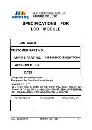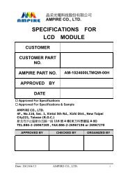
SPECIFICATIONS FOR LCD MODULE - OLED-LCD-TFT
SPECIFICATIONS FOR LCD MODULE - OLED-LCD-TFT
SPECIFICATIONS FOR LCD MODULE - OLED-LCD-TFT

Create successful ePaper yourself
Turn your PDF publications into a flip-book with our unique Google optimized e-Paper software.
Preliminary<br />
The contents of this document are confidential and must not be disclosed wholly<br />
or in part to any third part without the prior written consent of AMPIRE CO., LTD<br />
A M P I R E<br />
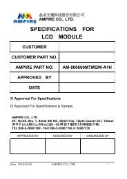
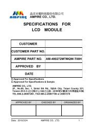
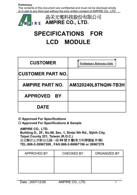
<strong>SPECIFICATIONS</strong> <strong>FOR</strong><br />
<strong>LCD</strong> <strong>MODULE</strong><br />
CUSTOMER<br />
CUSTOMER PART NO.<br />
AMPIRE PART NO. AM320240L8TNQW-TB3H<br />
APPROVED BY<br />
DATE<br />
Approved For Specifications<br />
Approved For Specifications & Sample<br />
UPreliminary Reference Only<br />
AMPIRE CO., LTD.<br />
Building D., 2F., No.88, Sec. 1, Sintai 5th Rd., Sijhih City,<br />
Taipei County 221, Taiwan (R.O.C.)<br />
台北縣汐止市新台五路一段 88 號 2 樓(東方科學園區 D 棟)<br />
TEL:886-2-26967269 , FAX:886-2-86967196 or 26967270<br />
APPROVED BY CHECKED BY ORGANIZED BY<br />
Date : 2007/12/28 AMPIRE CO., LTD. 1
Preliminary<br />
The contents of this document are confidential and must not be disclosed wholly<br />
or in part to any third part without the prior written consent of AMPIRE CO., LTD<br />
RECORD OF REVISION<br />
Revision Date Page Contents Editor<br />
2007/12/13<br />
2007/12/28<br />
--<br />
3<br />
New Release<br />
( 8 bit 80 interface + TP)<br />
Modify the Features.<br />
Edward<br />
Edward<br />
Date : 2007/12/28 AMPIRE CO., LTD. 2
Preliminary<br />
The contents of this document are confidential and must not be disclosed wholly<br />
or in part to any third part without the prior written consent of AMPIRE CO., LTD<br />
1 Features<br />
3.5 inch Amorphous-<strong>TFT</strong>-<strong>LCD</strong> (Thin Film Transistor Liquid Crystal Display)<br />
module. This module is composed of a 3.5” <strong>TFT</strong>-<strong>LCD</strong> panel, <strong>LCD</strong> controller and<br />
power driver circuit, Touch Panel and backlight unit.<br />
1.1 <strong>TFT</strong> Panel Feature :<br />
(1) Construction: 3.5” a-Si color <strong>TFT</strong>-<strong>LCD</strong>, White LED / CCFL Backlight<br />
and PCB.<br />
(2) Resolution (pixel): 320(R.G.B) X240<br />
(3) Number of the Colors : 262K colors ( R , G , B 6 bit digital each)<br />
(4) <strong>LCD</strong> type : Transmissive Color <strong>TFT</strong> <strong>LCD</strong> ( normally White)<br />
(5) Interface: 40 pin pitch 0.5 FFC<br />
(6) Power Supply Voltage: 3.3V single power input. Built-in power supply<br />
circuit.<br />
1.2 <strong>LCD</strong> Controller Feature:<br />
(1) MCU interface: 8 bit 80 series MCU interface.<br />
(2) Display RAM size: 640x240x3x6 bits. Ex: 320x240 two frame buffer<br />
with 262K colors.<br />
(3) Arbitrary display memory starts position selection.<br />
(4) 16 bit interface support 65K (R5 G6 B5) Color.<br />
2 Physical specifications<br />
Item Specifications Unit<br />
Display resolution(dot) 960 (W) x 240(H) dot<br />
Active area 70.08(W) x 52.56(H) mm<br />
Screen size 3.5(Diagonal) mm<br />
Pixel size 73 (W) x 219 (H) um<br />
Color configuration R.G.B stripe<br />
Overall dimension 77.8(W)x64(H) x 6.5(D) mm<br />
Weight T.B.D g<br />
Backlight unit LED<br />
Date : 2007/12/28 AMPIRE CO., LTD. 3
Preliminary<br />
The contents of this document are confidential and must not be disclosed wholly<br />
or in part to any third part without the prior written consent of AMPIRE CO., LTD<br />
3 Electrical specification<br />
3.1 Absolute max. ratings<br />
3.1.1 Electrical Absolute max. ratings<br />
Item Symbol Condition Min. Max. Unit Remark<br />
Power voltage VDD VSS=0 -0.3 5.5 V<br />
Input voltege VBinB -0.3 VDD+0.3 V Note 1<br />
Note1: /CS,/WR,/RD,RS,DB0~DN17<br />
3.1.2 Environmental Absolute max. ratings<br />
OPERATING STORAGE<br />
Item<br />
MIN MAX MIN MAX<br />
Remark<br />
Temperature -20 70 -30 80 Note2,3,4,5,6,7<br />
Humidity Note1 Note1<br />
Corrosive Gas Not Acceptable Not Acceptable<br />
Note1 : Ta 40℃ : Absolute humidity must be lower than the humidity of<br />
85%RH at 40℃<br />
Note2 : For storage condition Ta at -30℃ < 48h , at 80℃ < 100h<br />
For operating condition Ta at -20℃ < 100h<br />
Note3 : Background color changes slightly depending on ambient<br />
temperature. This phenomenon is reversible.<br />
Note4 : The response time will be slower at low temperature.<br />
Note5 : Only operation is guarantied at operating temperature. Contrast ,<br />
response time, another display quality are evaluated at +25℃<br />
Note6 :<br />
LED BL : When LCM is operated over 40℃ ambient temperature, the<br />
IBLEDB of the LED back-light should be follow :<br />
Date : 2007/12/28 AMPIRE CO., LTD. 4
Preliminary<br />
The contents of this document are confidential and must not be disclosed wholly<br />
or in part to any third part without the prior written consent of AMPIRE CO., LTD<br />
Note7 : This is panel surface temperature, not ambient temperature.<br />
Note8 :<br />
LED BL: When LCM be operated over than 40℃, the life time of the<br />
LED back-light will be reduced.<br />
3.1.3 LED back-light Unit Absolute max. ratings<br />
Item Symbol Ratings Unit Remark<br />
Peak forward Current IF 60 mA<br />
Reverse Voltage VR 15 V<br />
Power Dissipation Po 0.9 W<br />
3.2 Electrical characteristics<br />
3.2.1 DC Electrical characteristic of the <strong>LCD</strong><br />
Typical operting conditions (VSS=0V)<br />
Item Symbol Min. Typ. Max. Unit Remark<br />
Input Voltage<br />
Power supply VDD 3.0 3.3 5.0 V<br />
for logic<br />
Output Voltage for<br />
Logic<br />
H Level VBIHB 2.0 - 5.5 V<br />
L Level VBILB VSS - 0.8 V<br />
H Level VBOHB 2.4 - VDD V<br />
L Level VBOLB VSS 0.4 V<br />
Date : 2007/12/28 AMPIRE CO., LTD. 5<br />
Note 1<br />
Note 2<br />
Power Supply current IDD - 320 - mA Note 3<br />
Note1: With 5V Tolerance Input, /CS, /WR,/RD,RS,DB0~DB17<br />
Note2: DB0~DB17<br />
Note3: fV =60Hz, Ta=25℃, Display pattern: All Black
Preliminary<br />
The contents of this document are confidential and must not be disclosed wholly<br />
or in part to any third part without the prior written consent of AMPIRE CO., LTD<br />
3.2.2 Electrical characteristic of LED Back-light<br />
Paramenter Symbol Min. Typ. Max. Unit Condiction<br />
LED voltage VBAK B 9.0<br />
LED forward current<br />
- 11.0 V IBLEDB =40,Ta=25℃<br />
IBLEDB -- 40 -- mA Ta=25℃<br />
IBLEDB -- 30 -- mA Ta=60℃<br />
Lamp life time -- T.B.D. - Hr<br />
The constant current source is needed for white LED back-light driving.<br />
When LCM is operated over 60℃ ambient temperature, the IBLEDB of the LED<br />
back-light should be adjusted to 15mA max(For one dice LED).<br />
Date : 2007/12/28 AMPIRE CO., LTD. 6<br />
IBLEDB<br />
=40mA,Ta=25℃
Preliminary<br />
The contents of this document are confidential and must not be disclosed wholly<br />
or in part to any third part without the prior written consent of AMPIRE CO., LTD<br />
3.3 AC Timing characteristic of the Graphic <strong>TFT</strong> <strong>LCD</strong> controller<br />
Symbol Parameter Min Typ Max Unit Remark<br />
tcycle Enable cycle time 100 200 ns<br />
PWHW Enable high-level pulse width 66 70 ns<br />
PWLW Enable low-level pulse width 33 130 ns<br />
tAS RS setup time 16 25 ns<br />
tAH RS hold time 16 45 ns<br />
tDSW Write data setup time 50 50 ns<br />
tHWR Write data hold time 50 40 ns<br />
tcsb-s CSB setup time 16 20 ns<br />
tcsb-h CSB hold time 16 30 ns<br />
Date : 2007/12/28 AMPIRE CO., LTD. 7
Preliminary<br />
The contents of this document are confidential and must not be disclosed wholly<br />
or in part to any third part without the prior written consent of AMPIRE CO., LTD<br />
4 Optical specification<br />
Response<br />
Time<br />
4.1 Optical characteristic:<br />
Item Symbol Conditon Min. Typ. Max. Unit Remark<br />
Rise+<br />
Fall<br />
TBBr+BBTBBfBB Θ=0°<br />
Contrast ratio CR<br />
Viewing<br />
Angle<br />
Brightness<br />
LED BL<br />
Without TP<br />
Brightness<br />
LED BL<br />
With TP<br />
Top<br />
Bottom<br />
Left<br />
Right<br />
YBLB<br />
YBLB<br />
25 40 ms Note 1,2,3,5<br />
At optimized<br />
viewing angle<br />
CR≧ 10<br />
IBLEDB=40mA<br />
,25℃<br />
IBLEDB=40mA,<br />
25℃<br />
200 300 - Note 1,2,4,5<br />
Date : 2007/12/28 AMPIRE CO., LTD. 8<br />
-<br />
-<br />
-<br />
-<br />
35<br />
55<br />
70<br />
70<br />
-<br />
-<br />
-<br />
-<br />
330 350 -<br />
235 250 -<br />
deg. Note1,2, 5,6<br />
cd/<br />
2<br />
mP<br />
P<br />
cd/<br />
2<br />
mP<br />
P<br />
Note 7<br />
Note 7<br />
Red chromaticity<br />
Green chromaticity<br />
Blue chromaticity<br />
White chromaticity<br />
XR<br />
YR<br />
XG<br />
YG<br />
XB<br />
YB<br />
XW<br />
YW<br />
Θ=0°<br />
Θ=0°<br />
T.B.D.<br />
T.B.D.<br />
T.B.D.<br />
T.B.D.<br />
T.B.D.<br />
T.B.D.<br />
T.B.D.<br />
T.B.D.<br />
T.B.D.<br />
T.B.D.<br />
T.B.D.<br />
T.B.D.<br />
T.B.D.<br />
T.B.D.<br />
T.B.D.<br />
T.B.D.<br />
T.B.D.<br />
T.B.D.<br />
T.B.D.<br />
T.B.D.<br />
T.B.D.<br />
T.B.D.<br />
T.B.D.<br />
T.B.D.<br />
Note 7<br />
For reference<br />
only. These<br />
data should<br />
be update<br />
according the<br />
prototype.<br />
( ) For reference only. These data should be update according the prototype.<br />
Note 1:<br />
LED BL :Ambient temperature=25 ℃ ,and lamp current IBLEDB=40mA.To<br />
be<br />
measured in the dark room.<br />
Note 2:To be measured on the center area of panel with a viewing cone of 1°by<br />
Topcon luminance meter BM-7,after 10 minutes operation.<br />
Note 3.Definition of response time:<br />
The output signals of photo detector are measured when the input signals<br />
are changed from “black“ to “white”(falling time) and from “white” to<br />
“black”<br />
(rising time),respectively. The response time is defined as the time interval<br />
between the 10% and 90% of amplitudes. Refer to figure as below.
Preliminary<br />
The contents of this document are confidential and must not be disclosed wholly<br />
or in part to any third part without the prior written consent of AMPIRE CO., LTD<br />
Note 4.Definition of contrast ratio:<br />
Contrast ratio is calculated with the following formula.<br />
Contrast ratio(CR)=<br />
Photo detector output when <strong>LCD</strong> is at ”White” state<br />
Photo detector Output when <strong>LCD</strong> is at “Black” state<br />
Note 5:White VBiB=VBi50 B+1.5V<br />
Black VBiB=VBi50 B+2.0V<br />
“±”means that the analog input signal swings in phase with VBCOMB signal.<br />
“ “ means that the analog input signal swings out of phase with VBCOMB<br />
signal.<br />
VBi50B : The analog input voltage when transmission is 50%.The 100%<br />
Transmission is defined as the transmission of <strong>LCD</strong> panel when all the<br />
Input terminals of module are electrically opened.<br />
Note 6.Definition of viewing angle, Refer to figure as below.<br />
Date : 2007/12/28 AMPIRE CO., LTD. 9
Preliminary<br />
The contents of this document are confidential and must not be disclosed wholly<br />
or in part to any third part without the prior written consent of AMPIRE CO., LTD<br />
Note 7.Measured at the center area of the panel when all the input terminals of<br />
<strong>LCD</strong> panel are electrically opened.<br />
<strong>LCD</strong> module<br />
<strong>LCD</strong><br />
LED / CCFL<br />
Glass fiber<br />
Ring light<br />
LIGHT:OFF, LIGHT:ON<br />
Optical Detector<br />
LIGHT:ON, LIGHT:OFF<br />
Brightness gauge<br />
BM-7 (Topcon)<br />
Metal halide lamp<br />
Brightness gauge<br />
BM-7 (Topcon)<br />
Date : 2007/12/28 AMPIRE CO., LTD. 10
Preliminary<br />
The contents of this document are confidential and must not be disclosed wholly<br />
or in part to any third part without the prior written consent of AMPIRE CO., LTD<br />
4.2 Optical characteristic of the LED Back-light<br />
ITEM MIN TYP MAX UNIT Condition<br />
Bare Brightness - T.B.D. -- Cd/m2 IBLEDB =40mA,Ta=25℃<br />
AVG. X of 1931 C.I.E. 0.26 0.30 0.34 -- IBLEDB =40mA,Ta=25℃<br />
AVG. Y of 1931 C.I.E. 0.27 0.31 0.35 -- IBLEDB =40mA,Ta=25℃<br />
Brightness Uniformity 75 -- -- % IBLEDB =40mA,Ta=25℃<br />
( )For reference only. These data should be update according the prototype.<br />
Note1 : Measurement after 10 minutes from LED BL operating.<br />
Note2 : Measurement of the following 9 places on the display.<br />
Constant<br />
Current<br />
40mA<br />
A<br />
A<br />
K<br />
DC Current meter<br />
1/6W<br />
1/2W<br />
5/6W<br />
Date : 2007/12/28 AMPIRE CO., LTD. 11<br />
W<br />
1 2 3<br />
4 5 6<br />
7 8 9<br />
Note3: The Uniformity definition<br />
(Min Brightness / Max Brightness) x 100%<br />
1/6L<br />
1/2L<br />
5/6L<br />
L
Preliminary<br />
The contents of this document are confidential and must not be disclosed wholly<br />
or in part to any third part without the prior written consent of AMPIRE CO., LTD<br />
4.3 Touch Panel Electrical Specification<br />
Parameter Condition Standard Value<br />
Terminal Resistance<br />
X Axis<br />
Y Axis<br />
400 ~ 900 Ω<br />
200 ~ 500 Ω<br />
Insulating Resistance DC 25 V More than 10MΩ<br />
Linearity -- ±1.5 %<br />
Notes life by Pen Note a 100,000 times(min)<br />
Input life by finger Note b 1,000,000 times (min)<br />
Note A.<br />
Notes area for pen notes life test is 10 x 9 mm.<br />
Size of word is 7.5 x 6.72<br />
Shape of pen end: R0.8<br />
Load: 250 g<br />
Note B<br />
By Silicon rubber tapping at same point<br />
Shape of rubber end: R8<br />
Load: 200g<br />
Frequency: 5 Hz<br />
Interface<br />
No. Symbol Function<br />
1 X1 Touch Panel Right Signal in X Axis<br />
2 Y1 Touch Panel Upper Signal in Y Axis<br />
3 X2 Touch Panel Left Signal in X Axis<br />
4 Y2 Touch Panel Low Signal in Y Axis<br />
Date : 2007/12/28 AMPIRE CO., LTD. 12
Preliminary<br />
The contents of this document are confidential and must not be disclosed wholly<br />
or in part to any third part without the prior written consent of AMPIRE CO., LTD<br />
5 Interface specifications<br />
Pin no Symbol I/O Description Remark<br />
1<br />
2<br />
DGND - GND<br />
3 LED_A/PWM - LED Anode/LED dimming control(with LED driver IC).<br />
4 LED_K - LED Cathode<br />
5 /RESET I Reset signal for <strong>TFT</strong> <strong>LCD</strong> controller.<br />
6 RS I Register and Data select for <strong>TFT</strong> <strong>LCD</strong> controller.<br />
7 /CS506 I Chip select low active signal for <strong>TFT</strong> <strong>LCD</strong> controller.<br />
8 /WR<br />
80mode: /WR low active signal for <strong>TFT</strong> <strong>LCD</strong> controller.<br />
I<br />
68mode: E signal latch on rising edge.<br />
9 /RD<br />
80mode: /RD low active signal for <strong>TFT</strong> <strong>LCD</strong> controller.<br />
I<br />
68mode: R/W signal Hi: read, Lo: write.<br />
10 DB0 I<br />
11 DB1 I<br />
12 DB2 I<br />
13 DB3 I<br />
14 DB4 I<br />
15 DB5 I<br />
16 DB6 I<br />
17 DB7 I<br />
18<br />
19<br />
DB8<br />
DB9<br />
I<br />
I<br />
Data bus.<br />
20 DB10 I<br />
21 DB11 I<br />
22 DB12 I<br />
23 DB13 I<br />
24 DB14 I<br />
25 DB15 I<br />
26 DB16 I<br />
27 DB17 I<br />
28 262K/65K I Hi=262 K Color Mode; Lo: 65 K Color Mode.<br />
29 DGND - GND<br />
30 SK/X1<br />
Serial clock for Touch panel controller/<br />
I<br />
Touch Panel Right Signal in X Axis.<br />
31 DO/X2<br />
Data Output for Touch panel controller/<br />
I<br />
Touch Panel Left Signal in X Axis.<br />
32 DI/Y1<br />
Data In for Touch panel controller/<br />
I<br />
Touch Panel Upper Signal in Y Axis.<br />
33 TPCS/Y2<br />
Chip Select for Touch panel controller/<br />
I<br />
Touch Panel Lower Signal in Y Axis.<br />
34 IRQ I Interrupt for Touch panel controller.<br />
35-37 VDD - Power supply for the logic (3.3V).<br />
38-40 DGND - GND.<br />
29~34 : SK, DO, DI, CS, IRQ for Touch Panel controller TSC2046/<br />
X1, X2, Y1, Y2 for Touch Panel (without TSC2046)<br />
Date : 2007/12/28 AMPIRE CO., LTD. 13
Preliminary<br />
The contents of this document are confidential and must not be disclosed wholly<br />
or in part to any third part without the prior written consent of AMPIRE CO., LTD<br />
6 BLOCK DIAGRAM<br />
G1<br />
G240<br />
Power circuit<br />
FPC circuit<br />
320xRGBx240<br />
S960 S1<br />
VCOM<br />
DC/DC<br />
Gate Driver Circuit<br />
Power Supply Circuit<br />
Driving Circuit<br />
Output control<br />
SRAM<br />
640x240x6x6 bits<br />
SRAM control<br />
Input control<br />
VS<br />
HS<br />
DE<br />
DCLK<br />
R6<br />
G6<br />
B6<br />
<strong>TFT</strong> <strong>LCD</strong> controller<br />
<strong>TFT</strong> Panel<br />
LED/CCFL<br />
Back-light<br />
VDD<br />
VSS<br />
/RESET<br />
/WR (E)<br />
/RD(R/W)<br />
/CS<br />
RS<br />
DB0<br />
DB1<br />
DB2<br />
DB3<br />
DB4<br />
DB5<br />
DB6<br />
DB7<br />
DB8<br />
DB9<br />
DB10<br />
DB11<br />
DB12<br />
DB13<br />
DB14<br />
DB15<br />
DB16<br />
DB17<br />
262K/65K<br />
SK/X1<br />
DO/X2<br />
DI/Y1<br />
TPCS/Y2<br />
IRQ<br />
Date : 2007/12/28 AMPIRE CO., LTD. 14<br />
PLL<br />
OSC<br />
4<br />
Touch Panel<br />
TP controller<br />
/CS<strong>LCD</strong><br />
SDI<br />
SCK<br />
/RESET<br />
MCU<br />
A<br />
K
Preliminary<br />
The contents of this document are confidential and must not be disclosed wholly<br />
or in part to any third part without the prior written consent of AMPIRE CO., LTD<br />
7 Interface Protocol<br />
7.1 8Bit-80/68- Write to Command Register<br />
7.2 8Bit-80/68-Write to Display RAM<br />
80<br />
mode<br />
68<br />
mode<br />
/CS<br />
/RD<br />
/WR<br />
E<br />
R/W<br />
RS<br />
DB[7:0] Note1 Note2 Note3<br />
Display<br />
RAM<br />
Write Enable<br />
0x000C1<br />
Note1: DB[7:0] send 0x000C1 to Enable the Display RAM write.<br />
Note2: DB[7:0] represent the writing Data1 to Display RAM<br />
Note3: DB[7:0] represent the writing Data2 to Display RAM<br />
Note4: DB[7:0] represent the writing DataN to Display RAM<br />
Date : 2007/12/28 AMPIRE CO., LTD. 15<br />
Send<br />
Data1<br />
Send<br />
Data2<br />
Note5: DB[7:0] send 0x00080 to Disable the Display RAM write.<br />
Note4<br />
Send<br />
DataN<br />
Note5<br />
Display RAM<br />
Write Disable<br />
0x00080
Preliminary<br />
The contents of this document are confidential and must not be disclosed wholly<br />
or in part to any third part without the prior written consent of AMPIRE CO., LTD<br />
7.3 Data transfer order Setting<br />
7.3.1 18 bit interface 262K color only (Pin12 65K/262K =High)<br />
DB 17 16 15 14 13 12 11 10 9 8 7 6 5 4 3 2 1 0<br />
R5 R4 R3 R2 R1 R0 G5 G4 G3 G2 G1 G0 B5 B4 B3 B2 B1 B0<br />
7.3.2 16 bit interface 65K color (Pin12 65K/262K =Low)<br />
DB 15 14 13 12 11 10 9 8 7 6 5 4 3 2 1 0<br />
R4 R3 R2 R1 R0 G5 G4 G3 G2 G1 G0 B4 B3 B2 B1 B0<br />
7.3.3 16 bit interface 262K color (Pin12 65K/262K =High)<br />
DB 15 14 13 12 11 10 9 8 7 6 5 4 3 2 1 0<br />
st<br />
1P<br />
P data X X X X X X X X X X X X X X R5 R4<br />
nd<br />
2P<br />
P data R3 R2 R1 R0 G5 G4 G3 G2 G1 G0 B5 B4 B3 B2 B1 B0<br />
7.3.4 9 bit interface 262K color only (Pin12 65K/262K =High)<br />
DB 15 14 13 12 11 10 9 8 7 6 5 4 3 2 1 0<br />
st<br />
1P<br />
P data X X X X X X X R5 R4 R3 R2 R1 R0 G5 G4 G3<br />
nd<br />
2P<br />
P data X X X X X X X G2 G1 G0 B5 B4 B3 B2 B1 B0<br />
7.3.5 8 bit interface 65K color (Pin12 65K/262K =Low)<br />
DB 15 14 13 12 11 10 9 8 7 6 5 4 3 2 1 0<br />
st<br />
1P<br />
P data X X X X X X X X R4 R3 R2 R1 R0 G5 G4 G3<br />
nd<br />
2P<br />
P data X X X X X X X X G2 G1 G0 B4 B3 B2 B1 B0<br />
7.3.6 8 bit interface 262K color (Pin12 65K/262K =High)<br />
DB 15 14 13 12 11 10 9 8 7 6 5 4 3 2 1 0<br />
st<br />
1P<br />
P data X X X X X X X X R5 R4<br />
nd<br />
2P<br />
P data X X X X X X X X R3 R2 R1 R0 G5 G4 G3 G2<br />
rd<br />
3P<br />
P data X X X X X X X X G1 G0 B5 B4 B3 B2 B1 B0<br />
Date : 2007/12/28 AMPIRE CO., LTD. 16
Preliminary<br />
The contents of this document are confidential and must not be disclosed wholly<br />
or in part to any third part without the prior written consent of AMPIRE CO., LTD<br />
8 Register Depiction<br />
Register<br />
Address<br />
(Hex)<br />
Default<br />
(Hex)<br />
DB7 DB6 DB5 DB4 DB3 DB2 DB1 DB0 Remark<br />
00 00 MSB of X-axis start position<br />
Description set the horizontals start position of display active region<br />
Register<br />
Address<br />
(Hex)<br />
Default<br />
(Hex)<br />
DB7 DB6 DB5 DB4 DB3 DB2 DB1 DB0 Remark<br />
01 00 LSB of X-axis start position<br />
Description set the horizontals start position of display active region<br />
Register<br />
Address<br />
(Hex)<br />
Default<br />
(Hex)<br />
DB7 DB6 DB5 DB4 DB3 DB2 DB1 DB0 Remark<br />
02 01 MSB of X-axis end position<br />
Description set the horizontals end position of display active region<br />
Register<br />
Address<br />
(Hex)<br />
Default<br />
(Hex)<br />
DB7 DB6 DB5 DB4 DB3 DB2 DB1 DB0 Remark<br />
03 3F LSB of X-axis end position<br />
Description set the horizontals end position of display active region<br />
Register<br />
Address<br />
(Hex)<br />
Default<br />
(Hex)<br />
DB7 DB6 DB5 DB4 DB3 DB2 DB1 DB0 Remark<br />
04 00 MSB of Y-axis start position<br />
Description set the vertical start position of display active region<br />
Register<br />
Address<br />
(Hex)<br />
Default<br />
(Hex)<br />
DB7 DB6 DB5 DB4 DB3 DB2 DB1 DB0 Remark<br />
05 00 LSB of Y-axis start position<br />
Description Set the vertical start position of display active region<br />
Register<br />
Address<br />
(Hex)<br />
Default<br />
(Hex)<br />
DB7 DB6 DB5 DB4 DB3 DB2 DB1 DB0 Remark<br />
06 00 MSB of Y-axis end position<br />
Description set the vertical end position of display active region<br />
Register<br />
Address<br />
(Hex)<br />
Default<br />
(Hex)<br />
DB7 DB6 DB5 DB4 DB3 DB2 DB1 DB0 Remark<br />
07 EF LSB of Y-axis end position<br />
Description Set the vertical end position of display active region<br />
To simplify the address control of display RAM access, the window area address<br />
function<br />
allows for writing data only within a window area of display RAM specified by<br />
registers REG[00]~REG[07] .<br />
Date : 2007/12/28 AMPIRE CO., LTD. 17
Preliminary<br />
The contents of this document are confidential and must not be disclosed wholly<br />
or in part to any third part without the prior written consent of AMPIRE CO., LTD<br />
After writing data to the display RAM, the Address counter will be increased within<br />
setting window address-range which is specified by<br />
MIN X address (REG[0] & REG[1])<br />
MAX X address (REG[2] & REG[3])<br />
MIN Y address (REG[4] & REG[5])<br />
MAX Y address (REG[6] & REG[7])<br />
Therefore, data can be written consecutively without thinking the data address.<br />
Register<br />
Address<br />
(Hex)<br />
Default<br />
(Hex)<br />
DB7 DB6 DB5 DB4 DB3 DB2 DB1 DB0 Remark<br />
08 01 X X X X X X<br />
Description Set the panel X size<br />
Register<br />
Address<br />
(Hex)<br />
Default<br />
(Hex)<br />
_PanelXSize<br />
H_Byte[1:0]<br />
DB7 DB6 DB5 DB4 DB3 DB2 DB1 DB0 Remark<br />
09 40 _PanelXSize L_Byte[7:0]<br />
Description Set the panel X size<br />
The register REG[08] and REG[09] is use to calculate the RAM address. If you<br />
want to use the <strong>TFT</strong> as Landscape mode (320x240), the REG[08] & RGE[09 must<br />
set to 320. If you want to use the <strong>TFT</strong> as Portrait mode (240x320), the REG[08] &<br />
RGE[09] must set to 240.<br />
Date : 2007/12/28 AMPIRE CO., LTD. 18
Preliminary<br />
The contents of this document are confidential and must not be disclosed wholly<br />
or in part to any third part without the prior written consent of AMPIRE CO., LTD<br />
Register<br />
Address<br />
(Hex)<br />
Default<br />
(Hex)<br />
DB7 DB6 DB5 DB4 DB3 DB2 DB1 DB0 Remark<br />
0A 00 X X X X X<br />
Description Memory write start address<br />
Register<br />
Address<br />
(Hex)<br />
Default<br />
(Hex)<br />
[17:16] bits of<br />
memory write start<br />
address<br />
DB7 DB6 DB5 DB4 DB3 DB2 DB1 DB0 Remark<br />
0B 00 [15:8] bits of memory write start address<br />
Description Memory write start address<br />
Register<br />
Address<br />
(Hex)<br />
Default<br />
(Hex)<br />
DB7 DB6 DB5 DB4 DB3 DB2 DB1 DB0 Remark<br />
0C 00 [7:0] bits of memory write start address<br />
Description Memory write start address<br />
Register<br />
Address<br />
(Hex)<br />
Default<br />
(Hex)<br />
DB7 DB6 DB5 DB4 DB3 DB2 DB1 DB0 Remark<br />
0x10 0x0D Bit_SWAP OUT_TEST BUS_SEL Blanking P/S_SEL CLK_SEL<br />
Description<br />
"0x10_Clk_sel[1:0]" : The <strong>TFT</strong> controller built-in 40Mhz PLL clock. These bits<br />
are for select the <strong>TFT</strong> panel dot clock frequency.<br />
00 : 20Mhz 01: 10Mhz 02: 5 Mhz<br />
"0x10_ps_sel[2]" : The <strong>TFT</strong> controller support parallel and serial RGB<br />
interface. These bits are for select the output timing.<br />
0 : serial Panel 1: Parallel panel<br />
"0x10_blanking_tmp[3]"<br />
0 : OFF (blanking) 1: ON ( normal operation)<br />
"0x10_bus_sel[5:4]" : It only for serial Panel<br />
00=R , 01=G , 10=B<br />
"0x10_out_test[6]" : Self test<br />
0 : normal operation 1: for test (don’t use for normal operation)<br />
When set the bit to “1” , the Rout=(Reg 2a[6:0]) Gout=(Reg 2b[6:0])<br />
Bout=(Reg 2c[6:0])<br />
"0x10_bit_swap[7]" : 0-normal<br />
Date : 2007/12/28 AMPIRE CO., LTD. 19
Preliminary<br />
The contents of this document are confidential and must not be disclosed wholly<br />
or in part to any third part without the prior written consent of AMPIRE CO., LTD<br />
The default setting is suitable for AM320240N1. Don’t need to modify it.<br />
Register<br />
Address<br />
(Hex)<br />
Default<br />
(Hex)<br />
DB7 DB6 DB5 DB4 DB3 DB2 DB1 DB0 Remark<br />
0x11 00 X X EVEN _ODD<br />
Description<br />
Register<br />
Address<br />
(Hex)<br />
" Even line of serial panel data out sequence or data bus order of parallel<br />
panel<br />
000: RGB<br />
001: RBG<br />
010: GRB<br />
011: GBR<br />
100: BRG<br />
101: BGR<br />
Others: reserved<br />
Odd line of serial panel data out sequence<br />
000: RGB<br />
001: RBG<br />
010: GRB<br />
011: GBR<br />
100: BRG<br />
101: BGR<br />
Others: reserved<br />
Must Set to 0x05 for AM320240N1<br />
Default<br />
(Hex)<br />
DB7 DB6 DB5 DB4 DB3 DB2 DB1 DB0 Remark<br />
0x12 00 Hsync_stH_Byte[3:0]<br />
Description<br />
Register<br />
Address<br />
(Hex)<br />
For <strong>TFT</strong> output timing adjust:<br />
Hsync start position H-Byte<br />
The default setting is suitable for AM320240N1. Don’t need to modify it.<br />
Default<br />
(Hex)<br />
DB7 DB6 DB5 DB4 DB3 DB2 DB1 DB0 Remark<br />
0x13 00 Hsync_stL_Byte[7:0]<br />
Description<br />
Register<br />
Address<br />
(Hex)<br />
For <strong>TFT</strong> output timing adjust:<br />
Hsync start position L-Byte<br />
The default setting is suitable for AM320240N1. Don’t need to modify it.<br />
Default<br />
(Hex)<br />
DB7 DB6 DB5 DB4 DB3 DB2 DB1 DB0 Remark<br />
0x14 00 Hsync_pwH_Byte[3:0]<br />
Description<br />
Register<br />
Address<br />
(Hex)<br />
For <strong>TFT</strong> output timing adjust:<br />
Hsync pulse width H-Byte<br />
The default setting is suitable for AM320240N1. Don’t need to modify it.<br />
Default<br />
(Hex)<br />
DB7 DB6 DB5 DB4 DB3 DB2 DB1 DB0 Remark<br />
0x15 10 Hsync_pwL_Byte[7:0]<br />
Description<br />
For <strong>TFT</strong> output timing adjust:<br />
Hsync pulse width L-Byte<br />
Date : 2007/12/28 AMPIRE CO., LTD. 20
Preliminary<br />
The contents of this document are confidential and must not be disclosed wholly<br />
or in part to any third part without the prior written consent of AMPIRE CO., LTD<br />
The default setting is suitable for AM320240N1. Don’t need to modify it.<br />
Register<br />
Address<br />
(Hex)<br />
Default<br />
(Hex)<br />
DB7 DB6 DB5 DB4 DB3 DB2 DB1 DB0 Remark<br />
0x16 00 Hact_stH_Byte[3:0]<br />
Description<br />
Register<br />
Address<br />
(Hex)<br />
For <strong>TFT</strong> output timing adjust:<br />
DE pulse start position H-Byte<br />
The default setting is suitable for AM320240N1. Don’t need to modify it.<br />
Default<br />
(Hex)<br />
DB7 DB6 DB5 DB4 DB3 DB2 DB1 DB0 Remark<br />
0x17 38 Hact_stL_Byte[7:0]<br />
Description<br />
Register<br />
Address<br />
(Hex)<br />
For <strong>TFT</strong> output timing adjust:<br />
DE pulse start position L-Byte<br />
The default setting is suitable for AM320240N1. Don’t need to modify it.<br />
Default<br />
(Hex)<br />
DB7 DB6 DB5 DB4 DB3 DB2 DB1 DB0 Remark<br />
0x18 01 Hact_pwH_Byte[3:0]<br />
Description<br />
Register<br />
Address<br />
(Hex)<br />
For <strong>TFT</strong> output timing adjust:<br />
DE pulse width H-Byte<br />
The default setting is suitable for AM320240N1. Don’t need to modify it.<br />
Default<br />
(Hex)<br />
DB7 DB6 DB5 DB4 DB3 DB2 DB1 DB0 Remark<br />
0x19 40 Hact_pwL_Byte[7:0]<br />
Description<br />
Register<br />
Address<br />
(Hex)<br />
For <strong>TFT</strong> output timing adjust:<br />
DE pulse width L-Byte<br />
The default setting is suitable for AM320240N1. Don’t need to modify it.<br />
Default<br />
(Hex)<br />
DB7 DB6 DB5 DB4 DB3 DB2 DB1 DB0 Remark<br />
0x1A 01 HtotalH_Byte[3:0]<br />
Description<br />
Register<br />
Address<br />
(Hex)<br />
For <strong>TFT</strong> output timing adjust:<br />
Hsync total clocks H-Byte<br />
The default setting is suitable for AM320240N1. Don’t need to modify it.<br />
Default<br />
(Hex)<br />
DB7 DB6 DB5 DB4 DB3 DB2 DB1 DB0 Remark<br />
0x1B B8 HtotalL_Byte[7:0]<br />
Description<br />
Register<br />
Address<br />
(Hex)<br />
For <strong>TFT</strong> output timing adjust:<br />
Hsync total clocks H-Byte<br />
The default setting is suitable for AM320240N1. Don’t need to modify it.<br />
Default<br />
(Hex)<br />
DB7 DB6 DB5 DB4 DB3 DB2 DB1 DB0 Remark<br />
0x1C 00 Vsync_stH_Byte[3:0]<br />
Description<br />
For <strong>TFT</strong> output timing adjust:<br />
Vsync start position H-Byte<br />
The default setting is suitable for AM320240N1. Don’t need to modify it.<br />
Date : 2007/12/28 AMPIRE CO., LTD. 21
Preliminary<br />
The contents of this document are confidential and must not be disclosed wholly<br />
or in part to any third part without the prior written consent of AMPIRE CO., LTD<br />
Register<br />
Address<br />
(Hex)<br />
Default<br />
(Hex)<br />
DB7 DB6 DB5 DB4 DB3 DB2 DB1 DB0 Remark<br />
0x1D 00 Vsync_stL_Byte[7:0]<br />
Description<br />
Register<br />
Address<br />
(Hex)<br />
For <strong>TFT</strong> output timing adjust:<br />
Vsync start position L-Byte<br />
The default setting is suitable for AM320240N1. Don’t need to modify it.<br />
Default<br />
(Hex)<br />
DB7 DB6 DB5 DB4 DB3 DB2 DB1 DB0 Remark<br />
0x1E 00 Vsync_pwH_Byte[3:0]<br />
Description<br />
Register<br />
Address<br />
(Hex)<br />
For <strong>TFT</strong> output timing adjust:<br />
Vsync pulse width H-Byte<br />
The default setting is suitable for AM320240N1. Don’t need to modify it.<br />
Default<br />
(Hex)<br />
DB7 DB6 DB5 DB4 DB3 DB2 DB1 DB0 Remark<br />
0x1F 08 Vsync_pwL_Byte[7:0]<br />
Description<br />
Register<br />
Address<br />
(Hex)<br />
For <strong>TFT</strong> output timing adjust:<br />
Vsync pulse width L-Byte<br />
The default setting is suitable for AM320240N1. Don’t need to modify it.<br />
Default<br />
(Hex)<br />
DB7 DB6 DB5 DB4 DB3 DB2 DB1 DB0 Remark<br />
0x20 00 Vact_stH_Byte[3:0]<br />
Description<br />
Register<br />
Address<br />
(Hex)<br />
For <strong>TFT</strong> output timing adjust:<br />
Vertical DE pulse start position H-Byte<br />
The default setting is suitable for AM320240N1. Don’t need to modify it.<br />
Default<br />
(Hex)<br />
DB7 DB6 DB5 DB4 DB3 DB2 DB1 DB0 Remark<br />
0x21 12 Vact_stL_Byte[7:0]<br />
Description<br />
Register<br />
Address<br />
(Hex)<br />
For <strong>TFT</strong> output timing adjust:<br />
Vertical DE pulse start position L-Byte<br />
The default setting is suitable for AM320240N1. Don’t need to modify it.<br />
Default<br />
(Hex)<br />
DB7 DB6 DB5 DB4 DB3 DB2 DB1 DB0 Remark<br />
0x22 00 Vact_pwH_Byte[3:0]<br />
Description<br />
Register<br />
Address<br />
(Hex)<br />
For <strong>TFT</strong> output timing adjust:<br />
Vertical Active width H-Byte<br />
The default setting is suitable for AM320240N1. Don’t need to modify it.<br />
Default<br />
(Hex)<br />
DB7 DB6 DB5 DB4 DB3 DB2 DB1 DB0 Remark<br />
0x23 F0 Vact_pwL_Byte[7:0]<br />
Description<br />
For <strong>TFT</strong> output timing adjust:<br />
Vertical Active width H-Byte<br />
The default setting is suitable for AM320240N1. Don’t need to modify it.<br />
Date : 2007/12/28 AMPIRE CO., LTD. 22
Preliminary<br />
The contents of this document are confidential and must not be disclosed wholly<br />
or in part to any third part without the prior written consent of AMPIRE CO., LTD<br />
Register<br />
Address<br />
(Hex)<br />
Default<br />
(Hex)<br />
DB7 DB6 DB5 DB4 DB3 DB2 DB1 DB0 Remark<br />
0x24 01 VtotalH_Byte[3:0]<br />
Description<br />
Register<br />
Address<br />
(Hex)<br />
For <strong>TFT</strong> output timing adjust:<br />
Vertical total width H-Byte<br />
The default setting is suitable for AM320240N1. Don’t need to modify it.<br />
Default<br />
(Hex)<br />
DB7 DB6 DB5 DB4 DB3 DB2 DB1 DB0 Remark<br />
0x25 09 VtotalL_Byte[7:0]<br />
Description<br />
Register<br />
Address<br />
(Hex)<br />
For <strong>TFT</strong> output timing adjust:<br />
Vertical total width L-Byte<br />
The default setting is suitable for AM320240N1. Don’t need to modify it.<br />
Default<br />
(Hex)<br />
DB7 DB6 DB5 DB4 DB3 DB2 DB1 DB0 Remark<br />
26 00 X X X X X<br />
Description Memory read start address<br />
Register<br />
Address<br />
(Hex)<br />
Default<br />
(Hex)<br />
[17:16] bits of<br />
memory read start<br />
address<br />
DB7 DB6 DB5 DB4 DB3 DB2 DB1 DB0 Remark<br />
27 00 [15:8] bits of memory write start address<br />
Description Memory read start address<br />
Register<br />
Address<br />
(Hex)<br />
Default<br />
(Hex)<br />
DB7 DB6 DB5 DB4 DB3 DB2 DB1 DB0 Remark<br />
28 00 [7:0] bits of memory write start address<br />
Description Memory read start address<br />
Register<br />
Address<br />
(Hex)<br />
Default<br />
(Hex)<br />
DB7 DB6 DB5 DB4 DB3 DB2 DB1 DB0 Remark<br />
29 00 [7:1] Reversed<br />
Description [0] Load output timing related setting (H sync., V sync. and DE) to take effect<br />
Register<br />
Address<br />
(Hex)<br />
Default<br />
(Hex)<br />
DB7 DB6 DB5 DB4 DB3 DB2 DB1 DB0 Remark<br />
0x2A 00 X TestPatternRout[6:0]<br />
Description<br />
Register<br />
Address<br />
(Hex)<br />
When " REG[0x10]_out_test[6]" : Self test =1 ;<br />
The Rout data equal to TestPatternRout[6:0]<br />
Default<br />
(Hex)<br />
DB7 DB6 DB5 DB4 DB3 DB2 DB1 DB0 Remark<br />
0x2B 00 X TestPatternGout[6:0]<br />
When " REG[0x10]_out_test[6]" : Self test =1 ;<br />
Description<br />
The Gout data equal to TestPatternGout[6:0]<br />
Register Default DB7 DB6 DB5 DB4 DB3 DB2 DB1 DB0 Remark<br />
Date : 2007/12/28 AMPIRE CO., LTD. 23
Preliminary<br />
The contents of this document are confidential and must not be disclosed wholly<br />
or in part to any third part without the prior written consent of AMPIRE CO., LTD<br />
Address (Hex)<br />
(Hex)<br />
0x2C 00 X TestPatternBout[6:0]<br />
When " REG[0x10]_out_test[6]" : Self test =1 ;<br />
Description<br />
The Bout data equal to TestPatternBout[6:0]<br />
If you set the " REG[0x10]_out_test[6]" : Self test =1 , the <strong>TFT</strong> controller will skip<br />
the connect of the display RAM. The Output port will send the<br />
REG[2A] ,REG[2B],REG[2C] data.<br />
Register<br />
Address<br />
(Hex)<br />
Default<br />
(Hex)<br />
DB7 DB6 DB5 DB4 DB3 DB2 DB1 DB0 Remark<br />
Rising/falling _rotate<br />
0x2D 00 X X X X [3]<br />
edge[2] [1:0]<br />
[3] Output pin X_DCON level control ; <strong>TFT</strong> Power ON/OFF control<br />
0: <strong>TFT</strong> POWER circuit OFF<br />
1: <strong>TFT</strong> POWER circuit ON<br />
Rising/falling edge[2] :<br />
0: The RGB out put data are on the Rising edge of the DCLK.<br />
Description<br />
Register<br />
Address<br />
(Hex)<br />
1: The RGB out put data are on the Falling edge of the DCLK.<br />
_rotate [1:0]:<br />
00 : rotate 0 degree<br />
01 : rotate90 degree<br />
10 : rotate 270 degree<br />
11 : rotate 180 degree<br />
Default<br />
(Hex)<br />
DB7 DB6 DB5 DB4 DB3 DB2 DB1 DB0 Remark<br />
30 00 X X X X X<br />
Description Set the Horizontal offset<br />
Register<br />
Address<br />
(Hex)<br />
Default<br />
(Hex)<br />
_H byte<br />
H-Offset[3:0]<br />
DB7 DB6 DB5 DB4 DB3 DB2 DB1 DB0 Remark<br />
31 00 _L byte H-Offset[7:0]<br />
Description Set the Horizontal offset<br />
Register<br />
Address<br />
(Hex)<br />
Default<br />
(Hex)<br />
DB7 DB6 DB5 DB4 DB3 DB2 DB1 DB0 Remark<br />
32 00 X X X X X _H byte V-Offset[3:0]<br />
Description Set the Vertical offset<br />
Register<br />
Address<br />
Default<br />
(Hex)<br />
DB7 DB6 DB5 DB4 DB3 DB2 DB1 DB0 Remark<br />
Date : 2007/12/28 AMPIRE CO., LTD. 24
Preliminary<br />
The contents of this document are confidential and must not be disclosed wholly<br />
or in part to any third part without the prior written consent of AMPIRE CO., LTD<br />
(Hex)<br />
33 00 _L byte V-Offset[7:0]<br />
Description Set the Vertical offset<br />
Register<br />
Address<br />
(Hex)<br />
Default<br />
(Hex)<br />
DB7 DB6 DB5 DB4 DB3 DB2 DB1 DB0 Remark<br />
34 00 [7:4] Reserved _H byte H-def[3:0]<br />
Description [3:0] MSB of image horizontal physical resolution in memory<br />
Register<br />
Address<br />
(Hex)<br />
Default<br />
(Hex)<br />
DB7 DB6 DB5 DB4 DB3 DB2 DB1 DB0 Remark<br />
35 40 _L byte H-def[7:0]<br />
Description [7:0] LSB of image horizontal physical resolution in memory<br />
Register<br />
Address<br />
(Hex)<br />
Default<br />
(Hex)<br />
DB7 DB6 DB5 DB4 DB3 DB2 DB1 DB0 Remark<br />
36 01 [7:4] Reserved _H byte V-def[3:0]<br />
Description [3:0] MSB of image vertical physical resolution in memory<br />
Register<br />
Address<br />
(Hex)<br />
Default<br />
(Hex)<br />
DB7 DB6 DB5 DB4 DB3 DB2 DB1 DB0 Remark<br />
37 E0 _L byte V-def[7:0]<br />
Description [7:0] LSB of image vertical physical resolution in memory<br />
The total RAM size is 640x240x18bit. The user can arrange the Horizontal ram<br />
size by REG[34],REG[35] and the Vertical ram size by REG[36],REG[37].<br />
EX: 320x480x18bit REG[34]=0x01 , REG[35]=0x40 , REG[36]=0x01 ,<br />
REG[37]=0xE0<br />
EX: 640x240x18bit. REG[34]=0x02 , REG[35]=0x80 , REG[36]=0x00 ,<br />
REG[37]=0xF0<br />
Date : 2007/12/28 AMPIRE CO., LTD. 25
Preliminary<br />
The contents of this document are confidential and must not be disclosed wholly<br />
or in part to any third part without the prior written consent of AMPIRE CO., LTD<br />
9 Application Note:<br />
void main(void)<br />
{<br />
Initial_AMP506 ( );<br />
Full_386SCR(0xf800);<br />
Full_386SCR(0x07e0);<br />
Full_386SCR(0x001f);<br />
}<br />
void AMP506_80Mode_Command_SendAddress(BYTE Addr)<br />
{<br />
SET_nRD; // /RD=1<br />
CLR_RS; // RS=0<br />
CLR_CS1; // /CS=0<br />
CLR_nWRL; // /WR=0<br />
DB16OUT(Addr); // Data Bus OUT<br />
SET_nWRL; ///WR=1 /<br />
SET_RS; // RS=1<br />
SET_CS1;<br />
}<br />
// CS=1<br />
void AMP506_80Mode_Command_SendData(BYTE Data)<br />
{<br />
SET_nRD;<br />
SET_RS;<br />
CLR_CS1;<br />
CLR_nWRL;<br />
DB16OUT(Data);<br />
SET_nWRL;<br />
SET_RS;<br />
SET_CS1;<br />
}<br />
void AMP506_Command_Write(uint8 CMD_Address,uint8 CMD_Value)<br />
{<br />
AMP506_80Mode_Command_SendAddress(CMD_Address);<br />
AMP506_80Mode_Command_SendData(CMD_Value);<br />
}<br />
Date : 2007/12/28 AMPIRE CO., LTD. 26
Preliminary<br />
The contents of this document are confidential and must not be disclosed wholly<br />
or in part to any third part without the prior written consent of AMPIRE CO., LTD<br />
void AMP506_80Mode_16Bit_Memory_SendData(uint16 Dat16bit)<br />
{<br />
SET_nRD;<br />
SET_RS;<br />
CLR_CS1;<br />
CLR_nWRL;<br />
DB16OUT(Dat16bit>>8);<br />
SET_nWRL; // Low to High Latch Data to AMP506 Buffer<br />
SET_CS1;<br />
}<br />
SET_nRD;<br />
SET_RS;<br />
CLR_CS1;<br />
CLR_nWRL;<br />
DB16OUT(Dat16bit);<br />
SET_nWRL; // Low to High Latch Data to AMP506 Buffer<br />
SET_CS1;<br />
void Initial_AMP506(void)<br />
{<br />
AMP506_Command_Write(0x40,0x12); /*[7:6] Reserved<br />
[5] PLL control pins to select out frequency range<br />
0: 20MHz ~ 100MHz 1: 100MHz ~ 300MHz<br />
[4] Reserved [3] Reserved<br />
[2:1] Output Driving Capability<br />
00: 4mA 01: 8mA 10: 12mA 11: 16mA<br />
[0] Output slew rate<br />
0: Fast 1: Slow<br />
*/<br />
AMP506_Command_Write(0x41,0x01); //Set PLL=40Mhz * (0x42) / (0x41)<br />
AMP506_Command_Write(0x42,0x01); //0x41 [7:6] Reserved [5:0] PLL Programmable<br />
pre-divider, 6bit(1~63)<br />
//0x42 [7:6] Reserved [5:0] PLL Programmable loop<br />
divider, 6bit(1~63)<br />
AMP506_Command_Write(0x00,0x00); // MSB of horizontal start coordinate value<br />
AMP506_Command_Write(0x01,0x00); // LSB of horizontal start coordinate value<br />
Date : 2007/12/28 AMPIRE CO., LTD. 27
Preliminary<br />
The contents of this document are confidential and must not be disclosed wholly<br />
or in part to any third part without the prior written consent of AMPIRE CO., LTD<br />
AMP506_Command_Write(0x02,0x01); // MSB of horizontal end coordinate value<br />
AMP506_Command_Write(0x03,0x3F); // LSB of horizontal end coordinate value<br />
AMP506_Command_Write(0x04,0x00); // MSB of vertical start coordinate value<br />
AMP506_Command_Write(0x05,0x00); // LSB of vertical start coordinate value<br />
AMP506_Command_Write(0x06,0x01); // MSB of vertical end coordinate value<br />
AMP506_Command_Write(0x07,0x3F); // LSB of vertical end coordinate value<br />
AMP506_Command_Write(0x08,0x01); // MSB of input image horizontal resolution<br />
AMP506_Command_Write(0x09,0x40); // LSB of input image horizontal resolution<br />
AMP506_Command_Write(0x0a,0x00); //[17:16] bits of memory write start address<br />
AMP506_Command_Write(0x0b,0x00); //[15:8] bits of memory write start address<br />
AMP506_Command_Write(0x0c,0x00); //[7:0] bits of memory write start address<br />
AMP506_Command_Write(0x10,0x0D); /*[7] Output data bits swap 0: Normal 1:Swap<br />
[6] Output test mode enable 0: disable 1: enable<br />
[5:4] Serial mode data out bus selection<br />
00: X_ODATA17 ~ X_ODATA12 active , others are set to<br />
zero<br />
01: X_ODATA11 ~ X_ODATA06 active , others are set to<br />
zero<br />
10: X_ODATA05 ~ X_ODATA00 active , others are set to<br />
zero<br />
11: reserved<br />
[3] Output data blanking<br />
0: set output data to 0 1: Normal display<br />
[2] Parallel or serial mode selection<br />
0: serial data out 1: parallel data output<br />
[1:0] Output clock selection<br />
00: system clock divided by 2<br />
01: system clock divided by 4<br />
10: system clock divided by 8<br />
11: reserved */<br />
AMP506_Command_Write(0x11,0x05);<br />
/*[7] Reserved<br />
[6:4] Even line of serial panel data out sequence or data bus order of parallel panel<br />
000: RGB 001: RBG 010: GRB 011: GBR 100: BRG 101: BGR Others:<br />
reserved<br />
[3] Reversed<br />
[2:0] Odd line of serial panel data out sequence<br />
Date : 2007/12/28 AMPIRE CO., LTD. 28
Preliminary<br />
The contents of this document are confidential and must not be disclosed wholly<br />
or in part to any third part without the prior written consent of AMPIRE CO., LTD<br />
000: RGB 001: RBG 010: GRB 011: GBR 100: BRG 101: BGR Others:<br />
reserved */<br />
AMP506_Command_Write(0x12,0x00); // [3:0] MSB of output H sync. pulse start<br />
position<br />
AMP506_Command_Write(0x13,0x00); //[7:0] LSB of output H sync. pulse start position<br />
AMP506_Command_Write(0x14,0x00); // [3:0] MSB of output H sync. pulse width<br />
AMP506_Command_Write(0x15,0x10); //[7:0] LSB of output H sync. pulse width<br />
AMP506_Command_Write(0x16,0x00); //[3:0] MSB of output DE horizontal start<br />
position<br />
AMP506_Command_Write(0x17,0x38); //[7:0] LSB of output DE horizontal start<br />
position<br />
AMP506_Command_Write(0x18,0x01); //[3:0] MSB of output DE horizontal active region in<br />
pixel<br />
AMP506_Command_Write(0x19,0x40);<br />
in pixel<br />
//[7:0] LSB of output DE horizontal active region<br />
AMP506_Command_Write(0x1a,0x01);<br />
pixel<br />
//[7:4] Reserved [3:0] MSB of output H total in<br />
AMP506_Command_Write(0x1b,0xb8); //[7:0] LSB of output H total in pixel<br />
AMP506_Command_Write(0x1c,0x00);<br />
position<br />
//[3:0] MSB of output V sync. pulse start<br />
AMP506_Command_Write(0x1d,0x00); //[7:0] of output V sync. pulse start position<br />
AMP506_Command_Write(0x1e,0x00);<br />
pulse width<br />
//[7:4] Reserved [3:0] MSB of output V sync.<br />
AMP506_Command_Write(0x1f,0x08); //[7:0] LSB of output V sync. pulse width<br />
AMP506_Command_Write(0x20,0x00); // [3:0] MSB of output DE vertical start position<br />
AMP506_Command_Write(0x21,0x12); //[7:0] LSB of output DE vertical start position<br />
AMP506_Command_Write(0x22,0x00);<br />
in line<br />
// [3:0] MSB of output DE vertical active region<br />
AMP506_Command_Write(0x23,0xf0);<br />
in line<br />
//[7:0] LSB of output DE vertical active region<br />
AMP506_Command_Write(0x24,0x01);<br />
line<br />
//[7:4] Reversed [3:0] MSB of output V total in<br />
AMP506_Command_Write(0x25,0x09); //[7:0] LSB of output V total in line<br />
AMP506_Command_Write(0x26,0x00); // [17:16] bits of memory read start address<br />
AMP506_Command_Write(0x27,0x00); //[7:0] [15:8] bits of memory read start address<br />
AMP506_Command_Write(0x28,0x00); //[7:0] [7:0] bits of memory read start address<br />
AMP506_Command_Write(0x29,0x01);<br />
Date : 2007/12/28 AMPIRE CO., LTD. 29
Preliminary<br />
The contents of this document are confidential and must not be disclosed wholly<br />
or in part to any third part without the prior written consent of AMPIRE CO., LTD<br />
//[7:1] Reversed [0] Load output timing related setting (H sync., V sync. and DE) to take effect<br />
AMP506_Command_Write(0x2d,0x08); /* [7:4] Reserved<br />
[3] Output pin X_DCON level control<br />
[2] Output clock inversion 0: Normal 1: Inverse<br />
[1:0] Image rotate<br />
00: 0° 01: 90° 10: 270° 11: 180°<br />
*/<br />
AMP506_Command_Write(0x30,0x00); //[7:4] Reserved [3:0] MSB of image horizontal shift<br />
value<br />
AMP506_Command_Write(0x31,0x00); //[7:0] LSB of image horizontal shift value<br />
AMP506_Command_Write(0x32,0x00); //[7:4] Reserved [3:0] MSB of image vertical shift<br />
value<br />
AMP506_Command_Write(0x33,0x00); //[7:0] LSB of image vertical shift value<br />
AMP506_Command_Write(0x34,0x01);<br />
// [3:0] MSB of image horizontal physical Resolution in memory<br />
AMP506_Command_Write(0x35,0x40);<br />
//[7:0] LSB of image horizontal physical resolution in memory<br />
AMP506_Command_Write(0x36,0x01);<br />
//[7:4] Reserved [3:0] MSB of image vertical physical resolution in memory<br />
AMP506_Command_Write(0x37,0xe0);<br />
//[7:0] LSB of image vertical physical resolution in memory<br />
}<br />
void AMP506_WindowSet(uint16 S_X,uint16 S_Y,uint16 E_X,uint16 E_Y)<br />
{<br />
AMP506_80Mode_Command_SendAddress(0x00);<br />
AMP506_80Mode_Command_SendData((S_X)>>8);<br />
AMP506_80Mode_Command_SendData(S_X);<br />
AMP506_80Mode_Command_SendData((E_X-1)>>8);<br />
AMP506_80Mode_Command_SendData(E_X-1);<br />
AMP506_80Mode_Command_SendData(S_Y>>8);<br />
AMP506_80Mode_Command_SendData(S_Y);<br />
AMP506_80Mode_Command_SendData((E_Y-1)>>8);<br />
AMP506_80Mode_Command_SendData(E_Y-1);<br />
}<br />
void Full_386SCR(uint16 Dat16bit)<br />
Date : 2007/12/28 AMPIRE CO., LTD. 30
Preliminary<br />
The contents of this document are confidential and must not be disclosed wholly<br />
or in part to any third part without the prior written consent of AMPIRE CO., LTD<br />
{<br />
int32 k,l;<br />
AMP506_WindowSet(0,0,Resolution_X,Resolution_Y);<br />
AMP506_80Mode_Command_SendAddress(0xc1); //_DisplayRAM_WriteEnable_<br />
for(k=0;k
Preliminary<br />
The contents of this document are confidential and must not be disclosed wholly<br />
or in part to any third part without the prior written consent of AMPIRE CO., LTD<br />
9.5 Step5: Write the 640x240x18 bit data consecutively<br />
9.6 Step6: The display will show the following image.<br />
Date : 2007/12/28 AMPIRE CO., LTD. 32
Preliminary<br />
The contents of this document are confidential and must not be disclosed wholly<br />
or in part to any third part without the prior written consent of AMPIRE CO., LTD<br />
9.7 Step7: Change the Horizontal offset to switch or scroll the<br />
display data.<br />
Set the Horizontal offset = 160 , REG[30]=00 REG[31]=A0 . You will see<br />
9.8 Step8: Change the Horizontal offset to switch or scroll the<br />
display data.<br />
Set the Horizontal offset = 320 , REG[30]=01 REG[31]=40 . You will see<br />
Date : 2007/12/28 AMPIRE CO., LTD. 33
Basic<br />
Color<br />
Red<br />
Green<br />
Blue<br />
Preliminary<br />
The contents of this document are confidential and must not be disclosed wholly<br />
or in part to any third part without the prior written consent of AMPIRE CO., LTD<br />
DISPLAYED COLOR AND INPUT DATA<br />
Color &<br />
Gray<br />
DATA SIGNAL<br />
Scale R5 R4 R3 R2 R1 R0 G5 G4 G3 G2 G1 G0 B5 B4 B3 B2 B1 B0<br />
Black 0 0 0 0 0 0 0 0 0 0 0 0 0 0 0 0 0 0<br />
Red(0) 1 1 1 1 1 1 0 0 0 0 0 0 0 0 0 0 0 0<br />
Green(0) 0 0 0 0 0 0 1 1 1 1 1 1 0 0 0 0 0 0<br />
Blue(0) 0 0 0 0 0 0 0 0 0 0 0 0 1 1 1 1 1 1<br />
Cyan 0 0 0 0 0 0 1 1 1 1 1 1 1 1 1 1 1 1<br />
Magenta 1 1 1 1 1 1 0 0 0 0 0 0 1 1 1 1 1 1<br />
Yellow 1 1 1 1 1 1 1 1 1 1 1 1 0 0 0 0 0 0<br />
White 1 1 1 1 1 1 1 1 1 1 1 1 1 1 1 1 1 1<br />
Black 0 0 0 0 0 0 0 0 0 0 0 0 0 0 0 0 0 0<br />
Red(62) 0 0 0 0 0 1 0 0 0 0 0 0 0 0 0 0 0 0<br />
Red(61) 0 0 0 0 1 0 0 0 0 0 0 0 0 0 0 0 0 0<br />
: : : : : : : : : : : : : : : : : : :<br />
Red(31) 0 1 1 1 1 1 0 0 0 0 0 0 0 0 0 0 0 0<br />
: : : : : : : : : : : : : : : : : : :<br />
Red(1) 1 1 1 1 1 0 0 0 0 0 0 0 0 0 0 0 0 0<br />
Red(0) 1 1 1 1 1 1 0 0 0 0 0 0 0 0 0 0 0 0<br />
Black 0 0 0 0 0 0 0 0 0 0 0 0 0 0 0 0 0 0<br />
Green(62) 0 0 0 0 0 0 0 0 0 0 0 1 0 0 0 0 0 0<br />
Green(61) 0 0 0 0 0 0 0 0 0 0 1 0 0 0 0 0 0 0<br />
: : : : : : : : : : : : : : : : : : :<br />
Green(31) 0 0 0 0 0 0 0 1 1 1 1 0 0 0 0 0 0 0<br />
: : : : : : : : : : : : : : : : : : :<br />
Green(1) 0 0 0 0 0 0 1 1 1 1 1 0 0 0 0 0 0 0<br />
Green(0) 0 0 0 0 0 0 1 1 1 1 1 1 0 0 0 0 0 0<br />
Black 0 0 0 0 0 0 0 0 0 0 0 0 0 0 0 0 0 0<br />
Blue(62) 0 0 0 0 0 0 0 0 0 0 0 0 0 0 0 0 0 1<br />
Blue(61) 0 0 0 0 0 0 0 0 0 0 0 0 0 0 0 0 1 0<br />
: : : : : : : : : : : : : : : : : : :<br />
Blue(31) 0 0 0 0 0 0 0 0 0 0 0 0 0 1 1 1 1 1<br />
: : : : : : : : : : : : : : : : : : :<br />
Blue(1) 0 0 0 0 0 0 0 0 0 0 0 0 1 1 1 1 1 0<br />
Blue(0) 0 0 0 0 0 0 0 0 0 0 0 0 1 1 1 1 1 1<br />
Date : 2007/12/28 AMPIRE CO., LTD. 34
Preliminary<br />
The contents of this document are confidential and must not be disclosed wholly<br />
or in part to any third part without the prior written consent of AMPIRE CO., LTD<br />
10 QUALITY AND RELIABILITY<br />
10.1 TEST CONDITIONS<br />
Tests should be conducted under the following conditions :<br />
Ambient temperature : 25 ± 5°C<br />
Humidity : 60 ± 25% RH.<br />
10.2 SAMPLING PLAN<br />
Sampling method shall be in accordance with MIL-STD-105E , level II,<br />
normal single sampling plan .<br />
10.3 ACCEPTABLE QUALITY LEVEL<br />
A major defect is defined as one that could cause failure to or materially<br />
reduce the usability of the unit for its intended purpose. A minor defect is one that<br />
does not materially reduce the usability of the unit for its intended purpose or is an<br />
infringement from established standards and has no significant bearing on its<br />
effective use or operation.<br />
10.4 APPEARANCE<br />
An appearance test should be conducted by human sight at<br />
approximately 30 cm distance from the <strong>LCD</strong> module under flourescent light. The<br />
inspection area of <strong>LCD</strong> panel shall be within the range of following limits.<br />
Date : 2007/12/28 AMPIRE CO., LTD. 35
Preliminary<br />
The contents of this document are confidential and must not be disclosed wholly<br />
or in part to any third part without the prior written consent of AMPIRE CO., LTD<br />
10.5 INSPECTION QUALITY CRITERIA<br />
No. Item Criterion for defects Defect type<br />
1 Non display No non display is allowed Major<br />
2<br />
Irregular<br />
operation<br />
No irregular operation is allowed Major<br />
3 Short No short are allowed Major<br />
4 Open<br />
5<br />
6<br />
7<br />
8<br />
Black/White<br />
spot (I)<br />
Black/White<br />
line (I)<br />
Black/White<br />
sport (II)<br />
Black/White<br />
line (II)<br />
9 Back Light<br />
Any segments or common patterns that don’t activate<br />
are rejectable.<br />
Size D (mm) Acceptable number<br />
D U
Preliminary<br />
The contents of this document are confidential and must not be disclosed wholly<br />
or in part to any third part without the prior written consent of AMPIRE CO., LTD<br />
11<br />
12<br />
13<br />
14<br />
Blemish &<br />
Foreign matters<br />
Size:<br />
A + B<br />
D =<br />
2<br />
Scratch on<br />
Polarizer<br />
Bubble in<br />
polarizer<br />
Stains on<br />
<strong>LCD</strong> panel<br />
surface<br />
Size D (mm) Acceptable number<br />
D U
Preliminary<br />
The contents of this document are confidential and must not be disclosed wholly<br />
or in part to any third part without the prior written consent of AMPIRE CO., LTD<br />
The <strong>TFT</strong> panel may have bright dot or Dark dot.<br />
21 Defect Dot<br />
The acceptable number defection:<br />
Bright<br />
dot<br />
Dark dot Total dot<br />
Distance<br />
between<br />
2 3 4<br />
Dark-- dark<br />
L≧ 5 mm<br />
Minor<br />
11 Reliability test items :<br />
Test Item Test Conditions Note<br />
High Temperature Operation 70±3°C , t=96 hrs<br />
Low Temperature Operation -20±3°C , t=96 hrs<br />
High Temperature Storage 80±3°C , t=96 hrs 1,2<br />
Low Temperature Storage -30±3°C , t=96 hrs 1,2<br />
Humidity Test 40°C , Humidity 90%, 96 hrs 1,2<br />
-30°C ~ 25°C ~ 80°C<br />
Thermal Shock Test 30 min. 5 min. 30 min. ( 1 cycle )<br />
Total 5 cycle<br />
Sweep frequency:10~55~10 Hz/1min<br />
Vibration Test (Packing)<br />
Amplitude : 0.75mm<br />
Test direction : X.Y.Z/3 axis<br />
Duration : 30min/each axis<br />
150pF 330 ohm ±8kV, 10times air discharge<br />
Static Electricity<br />
150pF 330 ohm ±4kV, 10times contact discharge<br />
Note 1 : Condensation of water is not permitted on the module.<br />
Note 2 : The module should be inspected after 1 hour storage in normal<br />
conditions<br />
(15-35°C , 45-65%RH).<br />
Definitions of life end point :<br />
Current drain should be smaller than the specific value.<br />
Function of the module should be maintained.<br />
Appearance and display quality should not have degraded noticeably.<br />
Contrast ratio should be greater than 50% of the initial value.<br />
Date : 2007/12/28 AMPIRE CO., LTD. 38<br />
1,2<br />
2
Preliminary<br />
The contents of this document are confidential and must not be disclosed wholly<br />
or in part to any third part without the prior written consent of AMPIRE CO., LTD<br />
12 USE PRECAUTIONS<br />
12.1 Handling precautions<br />
1) The polarizing plate may break easily so be careful when handling it. Do not<br />
touch, press or rub it with a hard-material tool like tweezers.<br />
2) Do not touch the polarizing plate surface with bare hands so as not to make it<br />
dirty. If the surface or other related part of the polarizing plate is dirty, soak a<br />
soft cotton cloth or chamois leather in benzine and wipe off with it. Do not use<br />
chemical liquids such as acetone, toluene and isopropyl alcohol. Failure to do<br />
so may bring chemical reaction phenomena and deteriorations.<br />
3) Remove any spit or water immediately. If it is left for hours, the suffered part<br />
may deform or decolorize.<br />
4) If the <strong>LCD</strong> element breaks and any LC stuff leaks, do not suck or lick it. Also if<br />
LC stuff is stuck on your skin or clothing, wash thoroughly with soap and water<br />
immediately.<br />
12.2 Installing precautions<br />
1) The PCB has many ICs that may be damaged easily by static electricity. To<br />
prevent breaking by static electricity from the human body and clothing, earth<br />
the human body properly using the high resistance and discharge static<br />
electricity during the operation. In this case, however, the resistance value<br />
should be approx. 1MΩ and the resistance should be placed near the human<br />
body rather than the ground surface. When the indoor space is dry, static<br />
electricity may occur easily so be careful. We recommend the indoor space<br />
should be kept with humidity of 60% or more. When a soldering iron or other<br />
similar tool is used for assembly, be sure to earth it.<br />
2) When installing the module and ICs, do not bend or twist them. Failure to do<br />
so may crack LC element and cause circuit failure.<br />
3) To protect LC element, especially polarizing plate, use a transparent protective<br />
plate (e.g., acrylic plate, glass etc) for the product case.<br />
4) Do not use an adhesive like a both-side adhesive tape to make <strong>LCD</strong> surface<br />
(polarizing plate) and product case stick together. Failure to do so may cause<br />
the polarizing plate to peel off.<br />
12.3 Storage precautions<br />
1) Avoid a high temperature and humidity area. Keep the temperature between<br />
0°C and 35°C and also the humidity under 60%.<br />
2) Choose the dark spaces where the product is not exposed to direct sunlight or<br />
fluorescent light.<br />
Date : 2007/12/28 AMPIRE CO., LTD. 39
Preliminary<br />
The contents of this document are confidential and must not be disclosed wholly<br />
or in part to any third part without the prior written consent of AMPIRE CO., LTD<br />
3) Store the products as they are put in the boxes provided from us or in the<br />
same conditions as we recommend.<br />
12.4 Operating precautions<br />
1) Do not boost the applied drive voltage abnormally. Failure to do so may break<br />
ICs. When applying power voltage, check the electrical features beforehand<br />
and be careful. Always turn off the power to the LC module controller before<br />
removing or inserting the LC module input connector. If the input connector is<br />
removed or inserted while the power is turned on, the LC module internal<br />
circuit may break.<br />
2) The display response may be late if the operating temperature is under the<br />
normal standard, and the display may be out of order if it is above the normal<br />
standard. But this is not a failure; this will be restored if it is within the normal<br />
standard.<br />
3) The <strong>LCD</strong> contrast varies depending on the visual angle, ambient temperature,<br />
power voltage etc. Obtain the optimum contrast by adjusting the LC dive<br />
voltage.<br />
4) When carrying out the test, do not take the module out of the low-temperature<br />
space suddenly. Failure to do so will cause the module condensing, leading to<br />
malfunctions.<br />
5) Make certain that each signal noise level is within the standard (L level:<br />
0.2Vdd or less and H level: 0.8Vdd or more) even if the module has functioned<br />
properly. If it is beyond the standard, the module may often malfunction. In<br />
addition, always connect the module when making noise level measurements.<br />
6) The CMOS ICs are incorporated in the module and the pull-up and pull-down<br />
function is not adopted for the input so avoid putting the input signal open<br />
while the power is ON.<br />
7) The characteristic of the semiconductor element changes when it is exposed<br />
to light emissions, therefore ICs on the <strong>LCD</strong> may malfunction if they receive<br />
light emissions. To prevent these malfunctions, design and assemble ICs so<br />
that they are shielded from light emissions.<br />
8) Crosstalk occurs because of characteristics of the <strong>LCD</strong>. In general, crosstalk<br />
occurs when the regularized display is maintained. Also, crosstalk is affected<br />
by the LC drive voltage. Design the contents of the display, considering<br />
crosstalk.<br />
Date : 2007/12/28 AMPIRE CO., LTD. 40
Preliminary<br />
The contents of this document are confidential and must not be disclosed wholly<br />
or in part to any third part without the prior written consent of AMPIRE CO., LTD<br />
12.5 Other<br />
1) Do not disassemble or take the LC module into pieces. The LC modules once<br />
disassembled or taken into pieces are not the guarantee articles.<br />
2) The residual image may exist if the same display pattern is shown for hours.<br />
This residual image, however, disappears when another display pattern is<br />
shown or the drive is interrupted and left for a while. But this is not a problem<br />
on reliability.<br />
3) AMIPRE will provide one year warrantee for all products and three months<br />
warrantee for all repairing products.<br />
Date : 2007/12/28 AMPIRE CO., LTD. 41
Preliminary<br />
The contents of this document are confidential and must not be disclosed wholly<br />
or in part to any third part without the prior written consent of AMPIRE CO., LTD<br />
13 OUTLINE DIMENSION<br />
13.1 OUTLINE DIMENSION<br />
Date : 2007/12/28 AMPIRE CO., LTD. 42<br />
科技<br />
晶采 光 電