

Chapter 06 Camera Image Signal Processor.pdf
Chapter 06 Camera Image Signal Processor.pdf
Chapter 06 Camera Image Signal Processor.pdf

You also want an ePaper? Increase the reach of your titles
YUMPU automatically turns print PDFs into web optimized ePapers that Google loves.
Public Version<br />
<strong>Chapter</strong> 6<br />
SPRUGN4L–May 2010–Revised June 2011<br />
<strong>Camera</strong> <strong>Image</strong> <strong>Signal</strong> <strong>Processor</strong><br />
This chapter describes the camera image signal processor (ISP2P) in the device. ISP2P is backward<br />
compatible with ISP2 that is in the legacy device. To facilitate reading in this chapter, ISP2P will be<br />
referred to as ISP.<br />
NOTE: Some of the information in this chapter is © 2005-2008 MIPI Alliance, Inc. All rights<br />
reserved.<br />
MIPI Alliance Member Confidential.<br />
All rights reserved. This material is reprinted with the permission of the MIPI Alliance, Inc. No<br />
part(s) of this document may be disclosed, reproduced or used for any purpose other than as<br />
needed to support the use of the products of TI.<br />
See Device 37xx MIPI Disclaimer for details.<br />
NOTE: This chapter gives information about all modules and features in the high-tier device. To<br />
check availability of modules and features, see Section 1.5, AM/DM37x Family, and the<br />
device-specific data manual. In unavailable modules and features, the memory area is<br />
reserved, read is undefined, and write can lead to unpredictable behavior.<br />
Topic ........................................................................................................................... Page<br />
6.1 <strong>Camera</strong> ISP Overview ..................................................................................... 1070<br />
6.2 <strong>Camera</strong> ISP Environment ................................................................................ 1075<br />
6.3 <strong>Camera</strong> ISP Integration ................................................................................... 1123<br />
6.4 <strong>Camera</strong> ISP Functional Description .................................................................. 1138<br />
6.5 <strong>Camera</strong> ISP Basic Programming Model ............................................................ 1228<br />
6.6 <strong>Camera</strong> ISP Register Manual ........................................................................... 1286<br />
SPRUGN4L–May 2010–Revised June 2011 <strong>Camera</strong> <strong>Image</strong> <strong>Signal</strong> <strong>Processor</strong><br />
Copyright © 2010–2011, Texas Instruments Incorporated<br />
1<strong>06</strong>9
Public Version<br />
<strong>Camera</strong> ISP Overview www.ti.com<br />
6.1 <strong>Camera</strong> ISP Overview<br />
The camera ISP is a key component for imaging and video applications such as video preview, video<br />
record, and still-image capture with or without digital zooming.<br />
The camera ISP provides the system interface and the processing capability to connect RAW<br />
image-sensor modules to the device.<br />
The camera ISP implements three receivers which are named CSI2A, CSI1/CCP2B, and CSI2C. The<br />
CSI2A and CSI2C are MIPI® D-PHY CSI2 compatible. The CCP2B (compact camera port) is MIPI D-PHY<br />
CSI1 compatible if used in CSI1 mode. Moreover, on the outside boundaries of camera ISP before the<br />
mentioned above receivers, are located two MIPI D-PHY CSI2 compliant physical layers (CSIPHY1 and<br />
CSIPHY2). The two PHYs are MIPI CSI2 and MIPI CSI1/SMIA CCP2 compliant. Their purpose is to act as<br />
a physical connection between the outside pins for connecting external sensors and the internal receivers.<br />
By configuring the outside PHYs and feeding the receivers, the camera ISP supports up to two<br />
simultaneous pixel flows from external sensors. Only one of the data flow can use the Video processing<br />
hardware while the other must go to memory.<br />
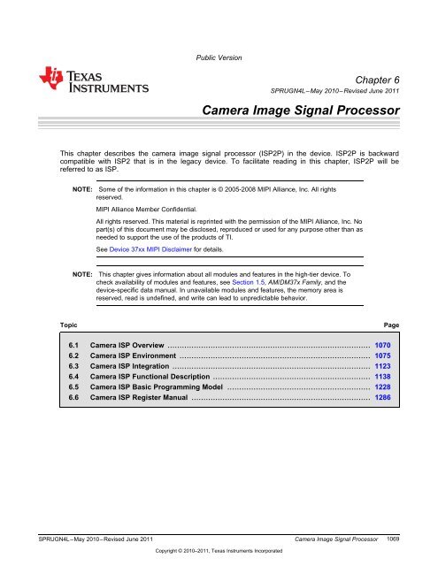
Figure 6-1 shows the camera ISP overview diagram.<br />
1070 <strong>Camera</strong> <strong>Image</strong> <strong>Signal</strong> <strong>Processor</strong> SPRUGN4L–May 2010–Revised June 2011<br />
Copyright © 2010–2011, Texas Instruments Incorporated
Device<br />
Legend:<br />
L4<br />
interconnect<br />
L3<br />
interconnect<br />
MPU<br />
subsystem<br />
INTC<br />
IVA2.2<br />
subsystem<br />
INTC<br />
PRCM<br />
STANDBY<br />
hardware<br />
handshake<br />
CAM_IRQ0<br />
CAM_IRQ1<br />
<strong>Camera</strong><br />
ISP<br />
CAM_MCLK<br />
CAM_ICLK<br />
CAM_FCLK<br />
CSI2_96M__FCLK<br />
Public Version<br />
www.ti.com <strong>Camera</strong> ISP Overview<br />
Figure 6-1. <strong>Camera</strong> ISP Overview Diagram<br />
CPI<br />
CSI2A<br />
CSI1 / CCP2B<br />
CSI2C<br />
CSIPHY1 CSIPHY2<br />
CPI input when PHY’s configured in GPI mode(cam_d signals)<br />
Serial-to-Parallel converted data stream<br />
cam_hs<br />
cam_vs<br />
cam_fld<br />
cam_wen<br />
cam_xclka<br />
cam_xclkb<br />
cam_pclk<br />
cam_d[11:10]<br />
cam_d[5:2]<br />
csi2_dx0 / ccpv2_dx0<br />
csi2_dy0 / ccpv2_dy0<br />
csi2_dx1 / ccpv2_dx1<br />
csi2_dy1 / ccpv2_dy1<br />
csi2_dx2 / cam_d[1]<br />
csi2_dy2 / cam_d[0]<br />
csi2_dx0 / ccpv2_dx0 / cam_d[6]<br />
csi2_dy0 / ccpv2_dy0 / cam_d[7]<br />
csi2_dx1 / ccpv2_dx1 / cam_d[8]<br />
csi2_dy1 / ccpv2_dy1 / cam_d[9]<br />
cam_strobe<br />
cam_global_reset<br />
cam_shutter<br />
(1) The mode for each PHY can be selected from CSI2, CSI1/CCP2B, and GPI at<br />
SCM.CONTROL_CAMERA_PHY_CTRL register. It can also control the connection between one of the<br />
PHY's and CSI1/CCP2B receiver via multiplexing.<br />
(2)<br />
(2)<br />
(1)(2)<br />
(1)(2)<br />
(1)(2)<br />
(1)(2)<br />
(1)(2)<br />
(1)(2)<br />
(1)(2)<br />
(1)(2)<br />
(1)(2)<br />
(1)(2)<br />
camisp-001<br />
(2) There is no top-level muxmode (padconf SCM register) control bit for the different camera modes supported<br />
by the interfaces. If one or another of the interfaces is enabled, then the camera input signals will be<br />
automatically routed to the corresponding ISP receiver depending on the PHY operating mode settings<br />
(SCM.CONTROL_CAMERA_PHY_CTRL register).<br />
NOTE: For information about initializing and configuring the CSIPHY, see Section 6.5.2,<br />
Programming the CSI1/CCP2B or CSI2 Receiver Associated PHY.<br />
SPRUGN4L–May 2010–Revised June 2011 <strong>Camera</strong> <strong>Image</strong> <strong>Signal</strong> <strong>Processor</strong><br />
Copyright © 2010–2011, Texas Instruments Incorporated<br />
1071
Public Version<br />
<strong>Camera</strong> ISP Overview www.ti.com<br />
6.1.1 <strong>Camera</strong> ISP Features<br />
The camera ISP can support the following features:<br />
• <strong>Image</strong> sensor:<br />
– Interface with various image sensors:<br />
• R, G, B primary colors<br />
• Ye, Cy, Mg, G complementary colors<br />
– Support for electronic rolling shutter (ERS) and global-release reset shutters<br />
• CSI1/CCP2B serial interface: The CSI1/CCP2B receiver is compatible with the SMIA CCP2<br />
specification and the MIPI CSI1 specification. It supports the following features:<br />
– <strong>Image</strong> from sensor<br />
• Transfer of pixels and data received by the associated PHY to system memory or to the Video<br />
processing hardware<br />
• Unidirectional data link<br />
• 1D and 2D addressing mode<br />
• Maximum data rate of up to 650 Mbps in CCP2 mode and 208 Mbps in CSI1 mode<br />
• False synchronization code protection<br />
• Ping-pong mechanism for double-buffering<br />
• Support of RGB, RAW, YUV, and JPEG formats<br />
• DPCM decompression supported<br />
– <strong>Image</strong> read from memory<br />
• RAW formats supported<br />
• Two MIPI CSI2 serial interfaces: The camera ISP implements two MIPI CSI2 serial interface<br />
receivers (CSI2A and CSI2C). The CSI2 receivers enables data transfer at up to 2Gbps. It is based on<br />
the MIPI CSI2 Specification 1.0.<br />
– Transfer pixels and data received by the CSIPHY1 or CSIPHY2 to the system memory or to the<br />
Video processing hardware<br />
– Uses unidirectional data link<br />
– Supports up to two data-configurable links, in addition to the clock signaling<br />
– Maximum data rate of up to 1000M bps per data lane<br />
– Data merger configuration for CSI2A two data lanes and CSI2C one data lane<br />
– Error detection and correction by the protocol engine<br />
– DMA engine integrated with dedicated FIFO<br />
– Streaming 1-D and 2-D addressing mode (rotation is not supported by the 2D mode)<br />
– Ping-pong mechanism for double buffering<br />
– Burst support<br />
– RAW frame transcoding. Including DPCM and A-law compression<br />
– JPEG support for unknown length transfer<br />
– RGB, RAW, and YUV formats supported<br />
– Storage in progressive mode for interlaced stream (using line numbering)<br />
– Conversion of the RGB formats<br />
– Configuration of the associated PHY through Serial Configuration Port (SCP)<br />
– Fully configurable interface of PHY: position of the clock and data and order of +/- differential<br />
signals for each pair.<br />
– Low power mode using PRCM protocols<br />
• Parallel interface: The camera parallel interface (CPI) supports two modes:<br />
– SYNC mode: In this mode, the image-sensor module provides horizontal and vertical<br />
synchronization signals to the parallel interface, along with the pixel clock. This mode works with 8-,<br />
10-, 11-, and 12-bit data (if using CCDC inside the Video processing hardware above 10 bit data<br />
must be internally converted to 10 bit by the Bridge lane shifter). SYNC mode supports progressive<br />
and interlaced image-sensor modules.<br />
– ITU mode: In this mode, the image-sensor module provides an ITU-R BT 656-compatible data<br />
stream. The horizontal and vertical synchronization signals are not provided to the interface.<br />
1072 <strong>Camera</strong> <strong>Image</strong> <strong>Signal</strong> <strong>Processor</strong> SPRUGN4L–May 2010–Revised June 2011<br />
Copyright © 2010–2011, Texas Instruments Incorporated
Public Version<br />
www.ti.com <strong>Camera</strong> ISP Overview<br />
Instead, the data stream embeds start-of-active video (SAV) and end-of-active video (EAV)<br />
synchronization code. This mode works in 8- and 10-bit configurations.<br />
• Video processing hardware: The Video processing hardware removes the need for expensive<br />
camera modules to perform processing functions. It consists of parts: front end and back end:<br />
– Video processing front end (VPFE): Performs signal-processing operations on RAW image input<br />
data. The output data can go directly to memory for software processing, or to the video-processing<br />
back end for further processing. The Video processing front end is supported by the CCDC module.<br />
<strong>Signal</strong>-processing operations include:<br />
• Optical clamping<br />
• Black-level compensation<br />
• Look-up table (LUT) based faulty pixel correction<br />
• 2D lens-shading compensation<br />
• Data formatter<br />
• Output formatter<br />
NOTE: Up to 12-bit data at 83 MHz can be transferred from the video port to the ISP<br />
submodules. The video processing ISP can treat one pixel every two interconnect clock<br />
cycles.<br />
– Video processing back end (VPBE): Performs signal-processing operations on RAW image input<br />
data. Outputs YCbCr 4:2:2 data.<br />
• Preview module: <strong>Signal</strong>-processing operations include:<br />
• A-law decompression: transforms non-linear 8-bit data to 10-bit linear data. The CCDC<br />
module can perform A-law compression<br />
• Noise reduction and faulty pixel correction<br />
• Dark frame capture and subtraction<br />
• Horizontal median filter<br />
• Programmable filter: 3x3 kernel of the same color<br />
• Couplet faulty pixel correction<br />
• Digital gain<br />
• White balance<br />
• Programmable color filter array (CFA) interpolation: 5x5 kernel<br />
• Black adjustment<br />
• Programmable color correction (RGB to RGB)<br />
• Programmable gamma correction: 1024 entries for each color<br />
• Programmable color conversion (RGB to YCbCr 4:4:4)<br />
• Color subsampling (YCbCr 4:4:4 to YCbCr 4:2:2)<br />
• Luminance enhancement (non-linear), chrominance suppression and offset<br />
The preview module can also work from memory to memory.<br />
• Resizer module: Performs on-the-fly upsampling (up to x4) and downsampling (down to x0.25)<br />
of YCbCr 4:2:2 data by applying high-quality horizontal and vertical filters. The horizontal and<br />
vertical resizer ratios are independent. Applicable ratios are 256/N, with N ranging from 64 to<br />
1024. This feature enables digital zooming (upsampling) and video preview (downsampling).<br />
The resizer module can also work from memory to memory. Higher or lower ratios can be<br />
obtained by combining on-the-fly resizing followed by memory-to-memory resizing.<br />
• Statistic collection modules (SCM): The host CPU uses statistics to adjust various parameters for<br />
processing image data.<br />
– 3A metrics: Collects on-the-fly RAW image data metrics, which are required to perform the control<br />
loops for auto white balance (AWB), auto exposure (AE), and autofocus (AF). The MPU subsystem<br />
typically uses data metrics to adjust various parameters for processing image data.<br />
– Histogram: Performs on-the-fly pixel binning of RAW image, based on color value ranges and<br />
regions. Supports up to 4 regions and up to 256 bins per color. The MPU subsystem typically uses<br />
the histogram with 3A metrics to adjust various parameters for processing image data.<br />
SPRUGN4L–May 2010–Revised June 2011 <strong>Camera</strong> <strong>Image</strong> <strong>Signal</strong> <strong>Processor</strong><br />
Copyright © 2010–2011, Texas Instruments Incorporated<br />
1073
Public Version<br />
<strong>Camera</strong> ISP Overview www.ti.com<br />
The histogram module can also work from memory to memory.<br />
• Central-resource shared buffer logic (SBL): Buffers and schedules memory accesses requested by<br />
camera ISP modules<br />
• Circular buffer: Prevents storage of full image frames in memory when data must be postprocessed<br />
and/or preprocessed by software<br />
• Memory management unit (MMU): Manages virtual-to-physical address translation for external<br />
addresses and solves the memory-fragmentation issue. Enables the camera driver to dynamically<br />
allocate and deallocate memory; the MMU handles memory fragmentation.<br />
• Clock generator: Generates two independent clocks that can be used by two external image sensors<br />
• Timing control:<br />
– Generation clocks passed to the clock generator<br />
– Generation of signals for strobe flash, mechanical shutter, and global reset. Support for red-eye<br />
removal.<br />
• Open core protocol (OCP) compliant:<br />
– One 64-bit master interface connected to L3<br />
– One 32-bit slave interface connected to L4<br />
1074 <strong>Camera</strong> <strong>Image</strong> <strong>Signal</strong> <strong>Processor</strong> SPRUGN4L–May 2010–Revised June 2011<br />
Copyright © 2010–2011, Texas Instruments Incorporated
Public Version<br />
www.ti.com <strong>Camera</strong> ISP Environment<br />
6.2 <strong>Camera</strong> ISP Environment<br />
6.2.1 <strong>Camera</strong> ISP Functions<br />
Table 6-1 describes the camera ISP functions and the corresponding application fields.<br />
Function Description<br />
Table 6-1. <strong>Camera</strong> ISP Functions<br />
Parallel interface in generic configuration The camera ISP supports up to 12 bits (If CCDC used inside the Video processing<br />
(SYNC mode) hardware, data must be converted to 10 bit by the Bridge lane shifter).<br />
The camera ISP can interface with RAW interlaced or progressive image sensors using<br />
RGB or complementary color mosaic filters.<br />
Parallel interface in ITU-R BT.656 The camera ISP can extract the synchronization signal start of active video and end of<br />
configuration (ITU mode) active video from the ITU-R BT.656 bit stream. 8-bit and 10-bit modes are supported.<br />
CSI1 / CCP2B serial interface The camera ISP supports one CCP2B serial interface, compatible MIPI CSI1.<br />
configuration<br />
(serial mode)<br />
MIPI CSI2 serial interfaces (CSI2A and The camera ISP supports two MIPI CSI2 serial interface.<br />
CSI2C) configuration (serial mode)<br />
NOTE: The two CSI2A and CSI2C receivers and the CSI1/CCP2B receiver can be active<br />
simultaneously. Either the CSIPHY1 or CSIPHY2 data can go through the selected interfaces<br />
to the video-processing hardware, while the other data are sent directly to memory by the<br />
receiver selected.<br />
The parallel interface is limited to 10 bits when used simultaneously with the CSI2A or CSI2C<br />
receivers.<br />
The parallel interface cannot be used simultaneously with the CSI1/CCP2B receiver.<br />
SPRUGN4L–May 2010–Revised June 2011 <strong>Camera</strong> <strong>Image</strong> <strong>Signal</strong> <strong>Processor</strong><br />
Copyright © 2010–2011, Texas Instruments Incorporated<br />
1075
Public Version<br />
<strong>Camera</strong> ISP Environment www.ti.com<br />
6.2.2 <strong>Camera</strong> ISP <strong>Signal</strong> Descriptions<br />
Table 6-2. IO Description<br />
Ball Name I/O (1) Description Parallel SYNC Parallel ITU Mode Serial Mode CSI\CCP2 Serial Mode CSI2<br />
Mode<br />
cam_hs I/O Line trigger input/output signal +<br />
cam_vs I/O Frame trigger input/output +<br />
signal<br />
cam_fld I/O Field identification input/output +<br />
signal<br />
cam_pclk I Parallel interface pixel clock + +<br />
cam_d[11:0] I Parallel mode: input data bits + +<br />
0 to 11<br />
cam_wen I External write-enable signal +<br />
cam_strobe O Flash strobe control signal + + + +<br />
cam_shutter O Mechanical shutter control + + + +<br />
signal<br />
cam_global_ I/O Global reset release shutter + + + +<br />
reset signal<br />
csi2_dx0 I Serial CSI2 mode: Fully +<br />
configurable pair: clock or<br />
data, positive or negative<br />
csi2_dy0 I Serial CSI2 mode: Fully +<br />
configurable pair: clock or<br />
data, positive or negative<br />
csi2_dx1 I Serial CSI2 mode: Fully +<br />
configurable pair: clock or<br />
data, positive or negative<br />
csi2_dy1 I Serial CSI2 mode: Fully +<br />
configurable pair: clock or<br />
data, positive or negative<br />
csi2_dx2 I Serial CSI2 mode: Fully +<br />
configurable pair: clock or<br />
data, positive or negative<br />
csi2_dy2 I Serial CSI2 mode: Fully +<br />
configurable pair: clock or<br />
data, positive or negative<br />
ccpv2_dx0 I Serial CSI/CCP2B mode: Fully +<br />
configurable pair: strobe or<br />
data, positive or negative<br />
(1)<br />
I = Input, O = Output, PWR = Power<br />
1076<strong>Camera</strong> <strong>Image</strong> <strong>Signal</strong> <strong>Processor</strong> SPRUGN4L–May 2010–Revised June 2011<br />
Copyright © 2010–2011, Texas Instruments Incorporated
Public Version<br />
www.ti.com <strong>Camera</strong> ISP Environment<br />
Table 6-2. IO Description (continued)<br />
Ball Name I/O (1) Description Parallel SYNC Parallel ITU Mode Serial Mode CSI\CCP2 Serial Mode CSI2<br />
Mode<br />
ccpv2_dy0 I Serial CSI/CCP2B mode: Fully +<br />
configurable pair: strobe or<br />
data, positive or negative<br />
ccpv2_dx1 I Serial CSI/CCP2B mode: Fully +<br />
configurable pair: strobe or<br />
data, positive or negative<br />
ccpv2_dy1 I Serial CSI1/CCP2B mode: +<br />
Fully configurable pair: strobe<br />
or data, positive or negative<br />
cam_xclka O External clock for the + + + +<br />
image-sensor module<br />
cam_xclkb O External clock for the + + + +<br />
image-sensor module<br />
6.2.3 <strong>Camera</strong> ISP Connectivity Schemes<br />
The cam_d[9:6] implements the CSIPHY1. The cam_d[1:0] implements the CSIPHY2. Moreover, the PHY's can be configured in GPI, CCP, or<br />
D-PHY modes from the control module and the SCM.CONTROL_CAMERA_PHY_CTRL control module register. Besides the mode set, from the<br />
SCM.CONTROL_CAMERA_PHY_CTRL[4] CSI1_RX_sel sets which PHY will be hooked to the CSI1/ CCP2B receiver of the ISP. Some<br />
initialization and pad configuration must also be done. For information about initializing and configuring the CSIPHY, see Section 6.5.2,<br />
Programming the CSI1/CCP2B or CSI2 Receiver Associated PHY.<br />
❏ In GPI mode, the PHY can be connected to a parallel camera (CAM_D[1:0] in CSIPHY1 and CAM_D[9:6] in CSIPHY2)<br />
❏ In CCP mode, the PHY can be connected to a CCPV2 camera (strobe/data pairs) or a CSI1 camera (clock/data pairs)<br />
❏ In D-PHY mode, the PHY can be connected to a CSI2 camera (2 or 1 data lane in CSIPHY1 and 1 data lane only in CSIPHY2)<br />
Table 6-3. <strong>Camera</strong> ISP Connectivity Schemes<br />
Receiver Scheme 1 Scheme 2 Scheme 3 Scheme 4 Scheme 5 Scheme 6<br />
Legacy Legacy Addon Legacy Addon Addon<br />
CPI ON, up to 10-bit ON, 12-bit ON, 12-bit OFF OFF OFF<br />
Serial CSI2A ON, CSI2A 2 data lanes ON, CSI2A 1 data lane OFF ON, CSI2A 2 data lanes ON, CSI2A 2 data lanes OFF<br />
Serial CSI1 / CCP2B OFF OFF ON, CSI1/ CCP2B 1 ON, CSI1/ CCP2B 1 OFF ON, CSI1/CCP2B 1<br />
data lane data lane data lane<br />
Serial CSI2C OFF OFF OFF OFF ON, CSI2C 1 data lanes OFF<br />
Data flows handling by ISP Simultaneous Simultaneous Simultaneous Simultaneous Simultaneous Sequential through<br />
control module selection<br />
SPRUGN4L–May 2010–Revised June 2011 <strong>Camera</strong> <strong>Image</strong> <strong>Signal</strong> <strong>Processor</strong>1077<br />
Copyright © 2010–2011, Texas Instruments Incorporated
Public Version<br />
<strong>Camera</strong> ISP Environment www.ti.com<br />
Table 6-3. <strong>Camera</strong> ISP Connectivity Schemes (continued)<br />
Receiver Scheme 1 Scheme 2 Scheme 3 Scheme 4 Scheme 5 Scheme 6<br />
cam_hs<br />
cam_vs<br />
cam_xclka CPI (1)<br />
cam_pclk<br />
cam_fld<br />
cam_d0/csi2_dx2<br />
cam_d1/csi2_dy2<br />
Legacy Legacy Addon Legacy Addon Addon<br />
CSI2A (2) (3) CSI2A (2) CSI2A (2)<br />
cam_d2 CPI CPI<br />
cam_d3<br />
cam_d4<br />
cam_d5<br />
cam_d6/ccpv2_dx0/csi2_dx0<br />
CPI<br />
cam_d7/ccpv2_dy0/csi2_dy0 CSI1/CCP2B with (5) (6)<br />
CSI1/CCP2B with<br />
CSI2C<br />
CSIPHY1 (4) cam_d8/ccpv2_dx1/csi2_dx1<br />
CSIPHY1<br />
cam_d9/ccpv2_dy1/csi2_dy1<br />
vdda_csiphy1 pwr rail VIO pwr rail VIO pwr rail VIO pwr rail VIO pwr rail CCP pwr rail CCP<br />
cam_d10<br />
cam_d11<br />
cam_xclkb CPI CPI CPI<br />
cam_wen<br />
cam_strobe<br />
csi2_dx0/ccpv2_dx0<br />
csi2_dy0/ccpv2_dy0 CSI1/CCP2B with CSI1/CCP2B with<br />
CSI2A (7) CSI2A (8) CSI2A (7) CSI2A (7)<br />
csi2_dx1/ccpv2_dx1<br />
CSIPHY2 CSIPHY2<br />
csi2_dy1/ccpv2_dy1<br />
vdda_csiphy2 pwr rail CSI pwr rail CSI pwr rail CCP pwr rail CSI pwr rail CSI pwr rail CSI<br />
(1) CPI Interface in orange<br />
(2) Full: All data/clock lines connected<br />
(3) CSI2A Interface in green<br />
(4) CSI1/CCP2B Interface in blue<br />
(5) Limited: Some data/clock lines connected<br />
(6) CSI2C Interface in green<br />
(7) Full: All data/clock lines connected<br />
(8) Limited: Some data/clock lines connected<br />
1078<strong>Camera</strong> <strong>Image</strong> <strong>Signal</strong> <strong>Processor</strong> SPRUGN4L–May 2010–Revised June 2011<br />
Copyright © 2010–2011, Texas Instruments Incorporated
Public Version<br />
www.ti.com <strong>Camera</strong> ISP Environment<br />
NOTE:<br />
• If the parallel camera sensor is the only sensor connected to one CSIPHY, the SCM.CONTROL_CAMERA0_PHY_CAMMOD and<br />
SCM.CONTROL_CAMERA1_PHY_CAMMOD bits must be set to 0x11 (that is, GPI mode).<br />
• If the parallel camera sensor and the other camera sensor (CCP2 or CSI2) are connected to the same CSIPHY, the<br />
CONTROL_CAMERAx_PHY_CAMMOD bit must be set for CCP2 or CSI2 mode, respectively, (even if only one pair is used as GPI<br />
for CPI mode). In that case, the corresponding CSI2_COMPLEXIO_CFG1.DATAx_POSITION bit must be set to 0x0 for the lane used<br />
in GPI mode.<br />
SPRUGN4L–May 2010–Revised June 2011 <strong>Camera</strong> <strong>Image</strong> <strong>Signal</strong> <strong>Processor</strong>1079<br />
Copyright © 2010–2011, Texas Instruments Incorporated
cam_pclk<br />
cam_hs<br />
cam_vs<br />
cam_pclk<br />
cam_vs<br />
cam_hs<br />
Public Version<br />
<strong>Camera</strong> ISP Environment www.ti.com<br />
6.2.4 <strong>Camera</strong> ISP Protocols and Data Formats<br />
6.2.4.1 <strong>Camera</strong> ISP Parallel Generic Configuration Protocol and Data Format (8, 10, 11, 12 Bits)<br />
The SYNC mode implements a generic parallel interface with the image sensor. The SYNC mode<br />
supports 8 to 12-bit-wide data signals.<br />
In this configuration, no assumptions are made on the data format of pixels, but the dynamic range is<br />
limited to 8-, 10-, 12 bit (data can be pure luminance for black and white sensor, RGB444, Bayer RGB,<br />
etc.). The pixel data is presented on cam_d, where one pixel is sampled for every cam_pclk rising edge<br />
(or falling edge, depending on the configuration of cam_pclk polarity). For more information, see<br />
Section 6.4.<br />
Additional pixel times between rows represent blanking periods. Active pixels are identified by a<br />
combination of two additional timing signals: horizontal synchronization (cam_hs) and vertical<br />
synchronization (cam_vs). During the image-sensor readout, these signals define when a row of valid data<br />
begins and ends, and when a frame starts and ends.<br />
NOTE: For correct operation, the clock cam_pclk must run during blanking periods (cam_hs and<br />
cam_vs inactive). cam_pclk must start before sending cam_d and start cam_vs and cam_hs.<br />
Figure 6-2 and Figure 6-3 show the frame and data timing, respectively, based on synchronization signals<br />
in the parallel No BT configuration.<br />
Figure 6-2. <strong>Camera</strong> ISP Synchronization <strong>Signal</strong>s and Frame Timing in SYNC Mode<br />
Figure 6-3. <strong>Camera</strong> ISP Synchronization <strong>Signal</strong>s and Data Timing in SYNC Mode<br />
cam_d Data 0 Data 1 Data 2<br />
NOTE: The pixel clock can be gated to qualify valid pixels. It can also be gated during blanking<br />
periods to reduce power consumption. However, at least 4 clock pulses are required before<br />
sending active image data and synchronization information; 8 clock pulses are required after<br />
the end of active video. Extra-clock pulses are allowed but not required during the line<br />
blanking periods.<br />
Figure 6-4 shows the timing diagram of the SYNC move clock gating.<br />
camisp-005<br />
camspi-0<strong>06</strong><br />
1080 <strong>Camera</strong> <strong>Image</strong> <strong>Signal</strong> <strong>Processor</strong> SPRUGN4L–May 2010–Revised June 2011<br />
Copyright © 2010–2011, Texas Instruments Incorporated
cam_pclk<br />
cam_hs<br />
cam_vs<br />
cam_fld<br />
cam_d<br />
4 pulses<br />
before start<br />
of frame<br />
required<br />
0 1 2 3 4 5 6 0 1 2 3 4 5 6<br />
0 1 2 3 4 5 6<br />
At the input of<br />
CCDC<br />
cam_vs must be<br />
active for at<br />
least one clock<br />
pulse to qualify<br />
start of frame<br />
cam_vs<br />
cam_hs<br />
cam_pclk<br />
cam_d<br />
VS<br />
WEN<br />
HS<br />
PCLK<br />
cam_hs must be<br />
inactive for at<br />
least one clock<br />
pulse between<br />
2 lines<br />
Public Version<br />
www.ti.com <strong>Camera</strong> ISP Environment<br />
Figure 6-4. <strong>Camera</strong> ISP SYNC Mode Clock Gating<br />
Data sampled on rising<br />
edge in this diagram.<br />
Programmable see<br />
register manual section.<br />
Extra pulses<br />
allowed but not<br />
required during<br />
blanking<br />
cam_hs must be<br />
active for at<br />
least one clock<br />
pulse to qualify<br />
start of line<br />
Timing of JPEG compressed data in free running clock mode<br />
8 pulses after<br />
end of frame<br />
required<br />
camisp-100<br />
Extra pulses<br />
between frames<br />
allowed but not<br />
required<br />
6.2.4.2 <strong>Camera</strong> ISP Parallel Generic Configuration: JPEG Sensor Connection on the Parallel Interface<br />
Some camera modules integrate an image-signal processor (ISP) and a JPEG encoder. The CCDC can<br />
interface with these camera modules and transfer the received JPEG stream to memory.<br />
To use this mode, set the ISP_CTRL [30] JPEG_FLUSH bit.<br />
Figure 6-5 shows timing diagrams for an JPEG stream.<br />
Figure 6-5. <strong>Camera</strong> ISP JPEG Stream Timing Diagrams<br />
CAUTION<br />
The bridge cannot be used for JPEG sensor connections.<br />
6.2.4.3 <strong>Camera</strong> ISP ITU-R BT.656 Protocol and Data Formats (8, 10 Bits)<br />
CAUTION<br />
The ITU-R BT.656 mode cannot be used when the bridge is enabled.<br />
The camera ISP interface supports data in ITU-R BT.656 format.<br />
SPRUGN4L–May 2010–Revised June 2011 <strong>Camera</strong> <strong>Image</strong> <strong>Signal</strong> <strong>Processor</strong><br />
Copyright © 2010–2011, Texas Instruments Incorporated<br />
camisp-132<br />
1081
cam_pclk<br />
Public Version<br />
<strong>Camera</strong> ISP Environment www.ti.com<br />
The ITU-R BT.656 standard specifies a method of transferring YUV422 data over an 8- or 10-bit video<br />
interface.<br />
Figure 6-6 shows the data timing diagram with embedded synchronization signal.<br />
Figure 6-6. <strong>Camera</strong> ISP Data Timing With Embedded Synchronization <strong>Signal</strong>s (8-Bit Case)<br />
cam_d[11:4] FFh 00h 00h XYh CB0 Y0 CR0<br />
camisp-007<br />
In BT.656, the data words (8- or 10-bit) in which the eight most-significant bits (MSBs) are all set to 1, or<br />
all set to 0 are reserved. Only 254 of the possible 256 8-bit word values, and 1016 of the possible 1024<br />
10-bit word values represent signal values.<br />
The data is multiplexed in the following order: Cb0 Y0 Cr0 Y1 Cb2 Y2 Cr2 Y3, etc., where the byte<br />
sequence Cb2n Y2n Cr2n refers to interleaved luminance and chroma samples and the following byte Y2n<br />
+ 1 corresponds to the next luminance sample.<br />
The BT.656 protocol uses unique timing reference signals embedded in the video stream. The<br />
synchronization signals cam_hs and cam_vs are not needed. This reduces the number of wires required<br />
for a BT.656 video interface.<br />
There are two timing reference codes: The start of active video (SAV) reference code precedes each<br />
video data block, and the end of active video (EAV) follows each video data block. Each timing reference<br />
signal consists of a 4-byte sequence in the following hexadecimal format: FF 00 00 XY. The first 3 bytes<br />
are a fixed preamble (see the ITU-R BT.656 specification). The fourth byte (XY) contains information<br />
defining field identification (F), blanking (V), and SAV/EAV information (H), and 4 parity bits calculated as<br />
a function of F, V, and H (see the ITU-R BT.656 specification).<br />
Table 6-4 lists the video timing reference codes for SAV and EAV.<br />
Table 6-4. <strong>Camera</strong> ISP Video Timing Reference Codes for SAV and EAV<br />
Data Bit Number First Word (FF) Second Word (00) Third Word (00) Fourth Word (XY)<br />
9 (MSB) 1 0 0 1<br />
8 1 0 0 F<br />
7 1 0 0 V<br />
6 1 0 0 H<br />
5 1 0 0 P3<br />
4 1 0 0 P2<br />
3 1 0 0 P1<br />
2 1 0 0 P0<br />
1 1 0 0 0<br />
0 1 0 0 0<br />
Table 6-5 contains a description of the F, V, and H signals.<br />
Table 6-5. <strong>Camera</strong> ISP F, V, H <strong>Signal</strong> Descriptions<br />
<strong>Signal</strong> Value Command<br />
F 0 Field 1<br />
1 Field 2<br />
V 0 0<br />
1 Vertical blank<br />
H 0 SAV<br />
1 EAV<br />
1082<strong>Camera</strong> <strong>Image</strong> <strong>Signal</strong> <strong>Processor</strong> SPRUGN4L–May 2010–Revised June 2011<br />
Copyright © 2010–2011, Texas Instruments Incorporated
Public Version<br />
www.ti.com <strong>Camera</strong> ISP Environment<br />
The resulting Hamming distance between any two code words is four, allowing two error detections and<br />
one error correction. To enable or disable the error-correcting capability, configure the CCDC_REC656IF<br />
[1] ECCFVH bit.<br />
NOTE: The 2-bit errors are detected, but not flagged or corrected. Errors of more than 2 bits are not<br />
corrected or flagged.<br />
Table 6-6 lists the F, V, and H protection (error-correction) bits.<br />
Table 6-6. <strong>Camera</strong> ISP F, V, H Protection (Error-Correction) Bits<br />
F V H P3 P2 P1 P0<br />
0 0 0 0 0 0 0<br />
0 0 1 1 1 0 1<br />
0 1 0 1 0 1 1<br />
0 1 1 0 1 1 0<br />
1 0 0 0 1 1 1<br />
1 0 1 1 0 1 0<br />
1 1 0 1 1 0 0<br />
1 1 1 0 0 0 1<br />
When operating in CCIR-656 mode, data is stored in SDRAM according to the format shown in Table 6-7<br />
when CCDC_SYN_MODE [11] PACK8 is enabled.<br />
Table 6-7. <strong>Camera</strong> ISP BT.656 Mode Data Format in SDRAM<br />
8 bit x 4 Pixel3 (Y1/Cr0) Pixel2 (Cr0/Y1) Pixel1 (Y0/Cb0) Pixel0 (Cb0/Y0)<br />
Bit 31 Bit 0<br />
NOTE: The CCDC outputs the XY code in the SAV and EAV into memory. To eliminate this, users<br />
must set the SPH register field to +1. In addition, the NPH register field must be set to<br />
accurately represent the number of active pixels.<br />
6.2.4.4 <strong>Camera</strong> ISP CSI1/CCP2 Protocol and Data Formats<br />
The CSI1/CCP2B receiver supports two protocols:<br />
• MIPI CSI1 protocol<br />
• CCP2 protocol<br />
The MIPI CSI1 protocol is compatible with the CCP2 protocol with the following constraints:<br />
• Class 0 CCP2 sensors are used: Data/clock<br />
• No RAW6 or RAW7 data types<br />
• No CRC code generation<br />
• Only one logical channel: Channel 0<br />
• No DPCM<br />
This section describes CSI1/CCP2B protocol and data formats. Table 6-8 describes the I/O for serial<br />
interface CSI1/CCP2B.<br />
Moreover, the CSI1/CCP2B receiver is a serial interface to an image sensor. Data is taken from pins and<br />
through the configured associated PHY taken to the receiver (for information about initializing and<br />
configuring the CSIPHY, see Section 6.5.2.2, <strong>Camera</strong> ISP CSIPHY Initialization for Work With<br />
CSI1/CCP2B Receiver). The receiver on its side, can send data to the Video processing hardware or<br />
memory.<br />
The CSI1/CCP2B receiver interface has several image-data operating modes, summarized in Table 6-8.<br />
SPRUGN4L–May 2010–Revised June 2011 <strong>Camera</strong> <strong>Image</strong> <strong>Signal</strong> <strong>Processor</strong><br />
Copyright © 2010–2011, Texas Instruments Incorporated<br />
1083
Public Version<br />
<strong>Camera</strong> ISP Environment www.ti.com<br />
(1)<br />
Table 6-8. <strong>Camera</strong> ISP CSI1/CCP2B <strong>Image</strong> Data Operating Modes and Alignment Constraints<br />
CCP2_LCx_ CCP2B Data OCP Bits per Width Storage 2D Mode Comments<br />
CTRL[7:3] Format Pixel (bpp) Constraint: Increase Versus Availability (1)<br />
Format (when sending Must Be a Packed<br />
data to memory, Multiple of n<br />
N/A when Pixels<br />
sending to VP)<br />
0x0 YUV422 big 16 8 N/A Yes<br />
endian<br />
0x1 YUV422 little 16 8 N/A Yes<br />
endian<br />
0x2 YUV420 12 32 N/A No<br />
0x3 YUV4:2:2 + VP N/A, data are 2 N/A N/A<br />
sent to VP<br />
0x3 RAW8 + VP N/A, data are 4 N/A N/A<br />
sent to VP<br />
0x4 RGB444 + 16 8 N/A Yes<br />
EXP16<br />
0x5 RGB565 16 8 N/A Yes<br />
0x6 RGB888 24 16 N/A No<br />
0x7 RGB888 + 32 4 N/A Yes<br />
EXP32<br />
0x8 RAW6 + EXP8 8 16 33% No CCP2 only<br />
0x9 RAW6 + 16 8 167% No DPCM<br />
DPCM10 + decompression<br />
EXP16 CCP2 only<br />
0xA RAW6 + N/A, data are 16 N/A N/A DPCM<br />
DPCM10 + VP sent to VP decompression<br />
CCP2 only<br />
0xB RAW10 - RAW6 6 64 40% No DPCM<br />
DPCM compression<br />
CCP2 only<br />
0xC RAW7 + EXP8 8 16 14% No CCP2 only<br />
0xD RAW7 + 16 8 129% No DPCM<br />
DPCM10 + decompression<br />
EXP16 CCP2 only<br />
0xE RAW7 + N/A, data are 32 N/A N/A DPCM<br />
DPCM10 + VP sent to VP decompression<br />
CCP2 only<br />
0xF RAW10 - RAW6 8 16 20% No DPCM<br />
DPCM + EXP8 compression<br />
CCP2 only<br />
0x10 RAW6 6 64 N/A No CCP2 only<br />
0x10 RAW7 7 128 N/A No CCP2 only<br />
0x10 RAW8 8 16 N/A No<br />
0x11 RAW8 + 16 8 100% No DPCM<br />
DPCM10 + decompression<br />
EXP16 CCP2 only<br />
0x12 RAW8 + N/A, data are 4 N/A N/A DPCM<br />
DPCM10 + VP sent to VP decompression<br />
CCP2 only<br />
0x13 RAW10 - RAW7 7 128 30% No DPCM<br />
DPCM compression<br />
CCP2 only<br />
0x14 RAW10 10 64 N/A No<br />
0x15 RAW10 + EXP16 16 8 60% No<br />
0x16 RAW10 + VP N/A, data are 16 N/A N/A<br />
sent to VP<br />
If data bigger than 10 bits and meant to be used by the CCDC, Bridge lane shifter must be configured for internal conversion to<br />
10 bits.<br />
1084<strong>Camera</strong> <strong>Image</strong> <strong>Signal</strong> <strong>Processor</strong> SPRUGN4L–May 2010–Revised June 2011<br />
Copyright © 2010–2011, Texas Instruments Incorporated
Every code is transmitted bytewise, LSB first.<br />
Example: code 0xFF00:0002<br />
First transmitted bit<br />
Public Version<br />
www.ti.com <strong>Camera</strong> ISP Environment<br />
Table 6-8. <strong>Camera</strong> ISP CSI1/CCP2B <strong>Image</strong> Data Operating Modes and Alignment Constraints<br />
(continued)<br />
CCP2_LCx_ CCP2B Data OCP Bits per Width Storage 2D Mode Comments<br />
CTRL[7:3] Format Pixel (bpp) Constraint: Increase Versus Availability (1)<br />
Format (when sending Must Be a Packed<br />
data to memory, Multiple of n<br />
N/A when Pixels<br />
sending to VP)<br />
0x17 RAW10 - RAW7 8 16 20% No DPCM<br />
DPCM + EXP8 compression<br />
CCP2 only<br />
0x18 RAW12 12 32 N/A No<br />
0x19 RAW12 + EXP16 16 8 33% No<br />
0x1A RAW12 + VP N/A, data are 8 N/A N/A<br />
sent to VP<br />
0x1B RAW10 - RAW8 8 16 20% No DPCM<br />
DPCM decompression<br />
CCP2 only<br />
0x1C JPEG, 8-bit data N/A N/A N/A No<br />
0x1D JPEG, 8-bit data N/A N/A N/A No<br />
+ FSP<br />
0x1E RAW10 - RAW8 8 16 20% No Data right shift<br />
NOTE:<br />
• EXP8 = Data expansion to 8 bits, padding with zeros<br />
• EXP16 = Data expansion to 16 bits, padding with alpha or zeros<br />
CCP2_LCx_CTRL [15:8] ALPHA can be used to set an alpha value.<br />
For RGB444 + EXP16:<br />
– data_out[31:28] = ALPHA[3:0] and data_out[27:16] = RGB444<br />
– data_out[15:12] = ALPHA[3:0] and data_out[11:0] = RGB444<br />
• EXP32 = Data expansion to 32 bits, padding with alpha<br />
CCP2_LCx_CTRL [15:8] ALPHA can be used to set an alpha value.<br />
For RGB888 + EXP32: data_out[31:24] = ALPHA[7:0] and data_out[23:0] = RGB888<br />
• FSP = False synchronization code protection decoding. Applies only to JPEG8 data<br />
format.<br />
• VP = Output to the video processing hardware is enabled. The programmer must ensure<br />
that only one logical channel is enabled to the Video processing hardware. The behavior<br />
of the video processing hardware is unpredictable if several logical channels to it are<br />
enabled simultaneously.<br />
The preamble 0xFF0000 is fixed by construction and must not be modified. However, the CSI1/CCP2B<br />
receiver programming model allows the synchronization code identifier to be overwritten: bits 0 to 3.<br />
Every code is transmitted bytewise, least-significant bit (LSB) first. For example, the code 0xFF00:0002<br />
transmitted from the image sensor corresponds to the following bitstream: 11111111 - 00000000 -<br />
00000000 - 01000000. Every default code starts with a set of eight 1s and sixteen 0s that are never<br />
received in pixel data. This means that content having eight 1s and sixteen 0s is not allowed. Figure 6-7<br />
shows an example of 0xFF00 0002 transmission.<br />
Figure 6-7. <strong>Camera</strong> ISP Example of 0xFF00 0002 Transmission<br />
1 1 1 1 1 1 1 1 0 0 0 0 0 0 0 0 0 0 0 0 0 0 0 0 0 1 0 0 0 0 0 0<br />
SPRUGN4L–May 2010–Revised June 2011 <strong>Camera</strong> <strong>Image</strong> <strong>Signal</strong> <strong>Processor</strong><br />
Copyright © 2010–2011, Texas Instruments Incorporated<br />
Time<br />
camisp-204<br />
1085
YUV422 big endian<br />
Transmitter<br />
u0 u1 u2 u3 u4 u5 u6 u7 y0 y1 y2 y3 y4 y5 y6 y7 v0 v1 v2 v3 v4 v5 v6 v7 y0 y1 y2 y3 y4 y5 y6 y7<br />
First transmitted bit<br />
Receiver<br />
u7 u6 u5 u4 u3 u2 u1 u0 y7 y6 y5 y4 y3 y2 y1 y0 v7 v6 v5 v4 v3 v2 v1 v0 y7 y6 y5 y4 y3 y2 y1 y0<br />
31 0<br />
Picture height<br />
u1 un+1 …<br />
Picture width = n<br />
y1 v1 y2 yn+1 vn+1 yn+2 u3 un+3 y3 yn+3 t0: VP_DATA[7:0] = [u7 u6 u5 u4 u3 u2 u1 u0]<br />
t1: VP_DATA[7:0] = [y7 y6 y5 y4 y3 y2 y1 y0]<br />
t2: VP_DATA[7:0] = [v7 v6 v5 v4 v3 v2 v1 v0]<br />
t3: VP_DATA[7:0] = [y7 y6 y5 y4 y3 y2 y1 y0]<br />
…<br />
…<br />
Odd lines<br />
Even lines<br />
Public Version<br />
<strong>Camera</strong> ISP Environment www.ti.com<br />
6.2.4.4.1 <strong>Camera</strong> ISP CSI1/CCP2 Pixel Data Format<br />
This section summarizes how the CSI1/CCP2B pixel data formats are transmitted over the serial interface<br />
and how the pixels are reconstructed, stored in memory, or passed to the video port.<br />
The CSI1/CCP2B receiver can cope with all data formats if the data line length sent through the<br />
associated PHY is a multiple of 32 bits. This condition is required for the CSI1/CCP2B receiver to work<br />
correctly.<br />
However, some data formats impose stronger line-length constraints to correctly finish pixel reconstruction<br />
at the end of the lines. If the additional constraints are not respected:<br />
• Only the last reconstructed pixels in every line are erroneous. The missing bits are replaced with 0s to<br />
perform pixel reconstruction.<br />
• The FW_IRQ interrupt is triggered.<br />
6.2.4.4.1.1 <strong>Camera</strong> ISP CSI1/CCP2 YUV Pixel Data Formats<br />
The YUV422 data format can be stored to memory in little- or big-endian format. The line length sent<br />
through the associated PHY must be a multiple of 32 bits.<br />
YUV422 data format can also be sent to the video port.<br />
YUV422 + VP is used to output RAW8 data to the video port: YUV422 + VP is equivalent to RAW8 + VP.<br />
Figure 6-8 and Figure 6-9 show big-endian and little-endian YUV422 format, respectively.<br />
Figure 6-8. <strong>Camera</strong> ISP CSI1/CCP2 YUV422 Big Endian<br />
u 1 y 1 v 1 y 2<br />
u 1 y 1 v 1 y 2<br />
First two pixels of first odd line are: {y ,v ,u } and {y ,v ,u }<br />
1 1 1 2 1 1<br />
time<br />
FIFO<br />
Data mem org<br />
First two pixels of first even line are: {y ,v ,u } and {y ,v ,u }<br />
n+1 n+1 n+1 n+2 n+1 n+1<br />
YUV4:2:2 + VP<br />
camisp-181<br />
1086 <strong>Camera</strong> <strong>Image</strong> <strong>Signal</strong> <strong>Processor</strong> SPRUGN4L–May 2010–Revised June 2011<br />
Copyright © 2010–2011, Texas Instruments Incorporated
YUV422 little endian<br />
Transmitter<br />
u0 u1 u2 u3 u4 u5 u6 u7 y0 y1 y2 y3 y4 y5 y6 y7 v0 v1 v2 v3 v4 v5 v6 v7 y0 y1 y2 y3 y4 y5 y6 y7<br />
First transmitted bit<br />
Receiver<br />
y7 y6 y5 y4 y3 y2 y1 y0 v7 v6 v5 v4 v3 v2 v1 v0 y7 y6 y5 y4 y3 y2 y1 y0 u7 u6 u5 u4 u3 u2 u1 u0<br />
31 0<br />
Picture height<br />
u 1<br />
…<br />
u 1<br />
y 2<br />
Picture width = n<br />
y1 v1 y2 u3 y3 un+1 yn+1 vn+1 yn+2 un+3 yn+3 t0: VP_DATA[7:0] = [u7 u6 u5 u4 u3 u2 u1 u0]<br />
t1: VP_DATA[7:0] = [y7 y6 y5 y4 y3 y2 y1 y0]<br />
t2: VP_DATA[7:0] = [v7 v6 v5 v4 v3 v2 v1 v0]<br />
t3: VP_DATA[7:0] = [y7 y6 y5 y4 y3 y2 y1 y0]<br />
y 1<br />
v 1<br />
…<br />
…<br />
Even lines<br />
Odd lines<br />
Public Version<br />
www.ti.com <strong>Camera</strong> ISP Environment<br />
Figure 6-9. <strong>Camera</strong> ISP CSI1/CCP2 YUV422 Little Endian<br />
v 1<br />
y 1<br />
First two pixels of first odd line are: {y ,v ,u } and {y ,v ,u }<br />
1 1 1 2 1 1<br />
time<br />
FIFO<br />
Data mem org<br />
First two pixels of first even line are: {y ,v ,u } and {y ,v ,u }<br />
n+1 n+1 n+1 n+2 n+1 n+1<br />
y 2<br />
u 1<br />
YUV4:2:2 + VP<br />
camisp-182<br />
The line length sent through the associated configured PHY is a multiple of 32 bits. Furthermore, the line<br />
length is a multiple of 3 x 32 bits and the number of lines is even to correctly finish the pixel<br />
reconstruction.<br />
The line structure is different for odd and even lines. Odd lines transport the U component, while even<br />
lines contain the V component. This is shown in Figure 6-10.<br />
SPRUGN4L–May 2010–Revised June 2011 <strong>Camera</strong> <strong>Image</strong> <strong>Signal</strong> <strong>Processor</strong><br />
Copyright © 2010–2011, Texas Instruments Incorporated<br />
1087
YUV420<br />
Transmitter<br />
u1 y1 y2 u3<br />
u0 u1 u2 u3 u4 u5 u6 u7 y0 y1 y2 y3 y4 y5 y6 y7 y0 y1 y2 y3 y4 y5 y6 y7 u0 u1 u2 u3 u4 u5 u6 u7<br />
t0 t31<br />
y3 y4 u5 y5<br />
y0 y1 y2 y3 y4 y5 y6 y7 y0 y1 y2 y3 y4 y5 y6 y7 u0 u1 u2 u3 u4 u5 u6 u7 y0 y1 y2 y3 y4 y5 y6 y7<br />
t32 t63<br />
y6 u7 y7 y8<br />
y0 y1 y2 y3 y4 y5 y6 y7 u0 u1 u2 u3 u4 u5 u6 u7 y0 y1 y2 y3 y4 y5 y6 y7 y0 y1 y2 y3 y4 y5 y6 y7<br />
t64 t95<br />
Receiver<br />
u3<br />
y2<br />
y1<br />
u1<br />
31 0<br />
u7 u6 u5 u4 u3 u2 u1 u0 y7 y6 y5 y4 y3 y2 y1 y0 y7 y6 y5 y4 y3 y2 y1 y0 u7 u6 u5 u4 u3 u2 u1 u0<br />
y5 u5<br />
y4 y3<br />
31 0<br />
y7 y6 y5 y4 y3 y2 y1 y0 u7 u6 u5 u4 u3 u2 u1 u0 y7 y6 y5 y4 y3 y2 y1 y0 y7 y6 y5 y4 y3 y2 y1 y0<br />
y8 y7 u7 y6<br />
31 0<br />
y7 y6 y5 y4 y3 y2 y1 y0 y7 y6 y5 y4 y3 y2 y1 y0 u7 u6 u5 u4 u3 u2 u1 u0 y7 y6 y5 y4 y3 y2 y1 y0<br />
Picture height<br />
Picture width = n<br />
y <br />
u y …<br />
v <br />
u v …<br />
y <br />
<br />
y <br />
y <br />
y <br />
y y <br />
u <br />
v <br />
u v y <br />
y <br />
y <br />
y <br />
Transmitted frame<br />
y <br />
y <br />
y <br />
y <br />
…<br />
…<br />
…<br />
Odd lines<br />
Even lines<br />
Public Version<br />
<strong>Camera</strong> ISP Environment www.ti.com<br />
Figure 6-10. <strong>Camera</strong> ISP CSI1/CCP2 YUV420<br />
6.2.4.4.1.2 <strong>Camera</strong> ISP CSI1/CCP2 RGB Pixel Data Formats<br />
First two pixels of first odd line are: {y1,v1,u1} and {y2,v1,u1}<br />
First two pixels of first even line are: {yn+1,v1,u1} and {yn+2,v1,u1}<br />
Time<br />
FIFO<br />
Data mem org<br />
camisp-183<br />
RGB888 data format can be output to memory in two formats: with no data expansion and with data<br />
expansion.<br />
If data expansion is used, the value of the 8 upper bits is programmable and can be set with an alpha<br />
value for computer graphics applications. The line length sent through the associated PHY is a multiple of<br />
32 bits. Furthermore, the line length is a multiple of 3 x 32 bits to correctly finish pixel reconstruction.<br />
Figure 6-11 shows an example of RGB888 format.<br />
1088 <strong>Camera</strong> <strong>Image</strong> <strong>Signal</strong> <strong>Processor</strong> SPRUGN4L–May 2010–Revised June 2011<br />
Copyright © 2010–2011, Texas Instruments Incorporated
RGB888<br />
Transmitter<br />
R 1 G1 B1 R2<br />
a0 a1 a2 a3 a4 a5 a6 a7 a0 a1 a2 a3 a4 a5 a6 a7 a0 a1 a2 a3 a4 a5 a6 a7 b0 b1 b2 b3 b4 b5 b6 b7<br />
G2 B 2 R 3 G 3<br />
b0 b1 b2 b3 b4 b5 b6 b7 b0 b1 b2 b3 b4 b5 b6 b7 c0 c1 c2 c3 c4 c5 c6 c7 c0 c1 c2 c3 c4 c5 c6 c7<br />
B 3 R 4 G4 B 4<br />
c0 c1 c2 c3 c4 c5 c6 c7 d0 d1 d2 d3 d4 d5 d6 d7 d0 d1 d2 d3 d4 d5 d6 d7 d0 d1 d2 d3 d4 d5 d6 d7<br />
Receiver<br />
Line width must be a multiple of three 32-bit words.<br />
Public Version<br />
www.ti.com <strong>Camera</strong> ISP Environment<br />
Figure 6-11. <strong>Camera</strong> ISP CSI1/CCP2 RGB888<br />
t0 t31<br />
t32 t63<br />
t64 t95<br />
R 2 B 1 G1 R1 31 0<br />
b7 b6 b5 b4 b3 b2 b1 b0 a7 a6 a5 a4 a3 a2 a1 a0 a7 a6 a5 a4 a3 a2 a1 a0 a7 a6 a5 a4 a3 a2 a1 a0<br />
G3 R 3 B2 G2 31 0<br />
c7 c6 c5 c4 c3 c2 c1 c0 c7 c6 c5 c4 c3 c2 c1 c0 b7 b6 b5 b4 b3 b2 b1 b0 b7 b6 b5 b4 b3 b2 b1 b0<br />
B 4 G4 R4 B3 31 0<br />
d7 d6 d5 d4 d3 d2 d1 d0 d7 d6 d5 d4 d3 d2 d1 d0 d7 d6 d5 d4 d3 d2 d1 d0 c7 c6 c5 c4 c3 c2 c1 c0<br />
B1 G1 R1 31 0<br />
0 0 0 0 0 0 0 0 a7 a6 a5 a4 a3 a2 a1 a0 a7 a6 a5 a4 a3 a2 a1 a0 a7 a6 a5 a4 a3 a2 a1 a0<br />
CCP2_LCx_CTRL[15:8] ALPHA (x = 0 to 3)<br />
FIFO<br />
Data mem org<br />
No data expansion<br />
B 2 G2 R 2<br />
31 0<br />
0 0 0 0 0 0 0 0 b7 b6 b5 b4 b3 b2 b1 b0 b7 b6 b5 b4 b3 b2 b1 b0 b7 b6 b5 b4 b3 b2 b1 b0<br />
FIFO<br />
31<br />
B 3 G3 R 3<br />
0<br />
Data mem org<br />
Data expansion<br />
0 0 0 0 0 0 0 0 c7 c6 c5 c4 c3 c2 c1 c0 c7 c6 c5 c4 c3 c2 c1 c0 c7 c6 c5 c4 c3 c2 c1 c0<br />
B 4 G4 R4 31 0<br />
0 0 0 0 0 0 0 0 d7 d6 d5 d4 d3 d2 d1 d0 d7 d6 d5 d4 d3 d2 d1 d0 d7 d6 d5 d4 d3 d2 d1 d0<br />
Time<br />
camisp-184<br />
For RGB565, the line length sent through the associated PHY is a multiple of 32 bits (see Figure 6-12).<br />
SPRUGN4L–May 2010–Revised June 2011 <strong>Camera</strong> <strong>Image</strong> <strong>Signal</strong> <strong>Processor</strong><br />
Copyright © 2010–2011, Texas Instruments Incorporated<br />
1089
RGB565<br />
Line width must be a multiple of one 32-bit word.<br />
Transmitter<br />
B1 G1 R1 B2 a0 a1 a2 a3 a4 a0 a1 a2 a3 a4 a5 a0 a1 a2 a3 a4 b0 b1 b2 b3 b4 b0 b1 b2 b3 b4 b5 b0 b1 b2 b3 b4<br />
First transmitted pixel<br />
Receiver<br />
R2 G2 B2 R1 G1 B1 31 0<br />
b4 b3 b2 b1 b0 b5 b4 b3 b2 b1 b0 b4 b3 b2 b1 b0 a4 a3 a2 a1 a0 a5 a4 a3 a2 a1 a0 a4 a3 a2 a1 a0<br />
RGB444<br />
Transmitter<br />
xx a0 a1 a2 a3 xx xx a0<br />
First transmitted pixel<br />
a1 a2 a3 xx a0 a1 a2 a3 xx b0 b1 b2 b3 xx xx b0 b1 b2 b3 xx b0 b1 b2 b3<br />
Receiver<br />
Public Version<br />
<strong>Camera</strong> ISP Environment www.ti.com<br />
Figure 6-12. <strong>Camera</strong> ISP CSI1/CCP2 RGB565<br />
Line width must be a multiple of one 32-bit word.<br />
B 1 G 1 R 1 B 2<br />
R2 G2 B2 R1 G1 B1 31 0<br />
0 0 0 0 b3 b2 b1 b0 b3 b2 b1 b0 b3 b2 b1 b0 0 0 0 0 a3 a2 a1 a0 a3 a2 a1 a0 a3 a2 a1 a0<br />
ALPHA ALPHA<br />
G 2<br />
G 2<br />
R 2<br />
R 2<br />
Time<br />
FIFO<br />
Data mem org<br />
camisp-185<br />
RGB444 data format is output to memory with data expansion. If data expansion is used, the value of the<br />
4 upper bits is programmable and can be set with an alpha value for computer graphics applications. The<br />
line length sent through the associated PHY is a multiple of 32 bits (see Figure 6-13).<br />
Figure 6-13. <strong>Camera</strong> ISP CSI1/CCP2 RGB444<br />
6.2.4.4.1.3 <strong>Camera</strong> ISP CSI1/CCP2 RAW Bayer RGB Pixel Data Formats<br />
6.2.4.4.1.3.1 <strong>Camera</strong> ISP CSI1/CCP2 RAW6 (CCP2 Only)<br />
Time<br />
FIFO<br />
Data mem org<br />
RAW6 data format can be output to memory in two formats: with no data expansion and with data<br />
expansion.<br />
camisp-186<br />
The line length sent through the associated PHY is a multiple of 32 bits. Furthermore, the line is a multiple<br />
of 3 x 32 bits to correctly finish pixel reconstruction (the lowest common multiple of 32 and 6 is 96; that is<br />
3 x 32 bits).<br />
Figure 6-14 shows RAW6 format.<br />
NOTE: The RAW6 data format do not apply to the MIPI CSI1 compatible mode.<br />
1090 <strong>Camera</strong> <strong>Image</strong> <strong>Signal</strong> <strong>Processor</strong> SPRUGN4L–May 2010–Revised June 2011<br />
Copyright © 2010–2011, Texas Instruments Incorporated
RAW6<br />
Transmitter<br />
a1 a2 a3 a4 a5 b0 b1 b2<br />
b3 b4 b5 c0 c1 c2 c3 c4 c5 d0 d1 d2 d3 d4 d5 e0 e1 e2 e3 e4 e5 f0 f1<br />
First transmitted bit<br />
Receiver<br />
Line width must be a multiple of three 32-bit words.<br />
Pixel 1 Pixel 2 Pixel 3 Pixel 4<br />
31<br />
0<br />
Pixel 4<br />
0 d5 d4 d3 d2 d1 d0 0<br />
Pixel 3 Pixel 2 Pixel 1<br />
0<br />
0 c5 c4 c3 c2 c1 c0 0 0 b5 b4 b3 b2 b1 b0 0 0 a5 a4 a3 a2 a1 a0<br />
FIFO<br />
Data mem org<br />
Data expansion<br />
RAW6+EXP8<br />
Pixel 2 Pixel 1<br />
31 0<br />
0 0 0 0 0 0 b9 b8 b7 b6 b5 b4 b3 b2 b1 b0 0 0 0 0 0 0 a9 a8 a7 a6 a5 a4 a3 a2 a1 a0<br />
Pixel 4 Pixel 3<br />
FIFO<br />
Data mem org<br />
Data expansion<br />
0 0 0 0 0 0 d9 d8 d7 d6 d5 d4 d3 d2 d1 d0 0 0 0 0 0 0 c9 c8 c7 c6 c5 c4 c3 c2 c1 c0<br />
RAW6+DPCM10+EXP16<br />
t0: VP_DATA[9:0] = [a9 a8 a7 a6 a5 a4 a3 a2 a1 a0]<br />
t1: VP_DATA[9:0] = [b9 b8 b7 b6 b5 b4 b3 b2 b1 b0]<br />
t2: VP_DATA[9:0] = [c9 c8 c7 c6 c5 c4 c3 c2 c1 c0]<br />
t3: VP_DATA[9:0] = [d9 d8 d7 d6 d5 d4 d3 d2 d1 d0]<br />
Public Version<br />
www.ti.com <strong>Camera</strong> ISP Environment<br />
Figure 6-14. <strong>Camera</strong> ISP CSI1/CCP2 RAW 6<br />
6.2.4.4.1.3.2 <strong>Camera</strong> ISP CSI1/CCP2 RAW7 (CCP2 Only)<br />
Pixel 5<br />
Time<br />
RAW6+DPCM10+VP<br />
RAW7 data format can be output to memory in two formats: with no data expansion and with data<br />
expansion.<br />
camisp-187<br />
The line length sent through the associated PHY is a multiple of 32 bits. Furthermore, the line length is a<br />
multiple of 7 x 32 bits to correctly finish the pixel reconstruction (the lowest common multiple of 32 and 7<br />
is 224; that is, 7 x 32 bits).<br />
Figure 6-15 shows RAW7 format.<br />
NOTE: The RAW7 data format do not apply to the MIPI CSI1 compatible mode.<br />
SPRUGN4L–May 2010–Revised June 2011 <strong>Camera</strong> <strong>Image</strong> <strong>Signal</strong> <strong>Processor</strong><br />
Copyright © 2010–2011, Texas Instruments Incorporated<br />
1091
RAW7<br />
Transmitter<br />
a0 a1 a2 a3 a4 a5 a6 b0 b1 b2 b3 b4 b5 b6 c0 c1 c2 c3 c4 c5 c6 d0 d1 d2 d3 d4 d5 d6 e0 e1 e2 e3<br />
First transmitted bit<br />
Line width must be a multiple of seven 32-bit words.<br />
Pixel 1 Pixel 2 Pixel 3 Pixel 4<br />
Receiver<br />
Pixel 4<br />
31<br />
0 d6 d5 d4 d3 d2 d1 d0<br />
Pixel 3<br />
0 c6 c5 c4 c3 c2 c1 c0<br />
Pixel 2 Pixel 1<br />
0<br />
0 b6 b5 b4 b3 b2 b1 b0 0 a6 a5 a4 a3 a2 a1 a0<br />
FIFO<br />
Data mem org<br />
Data expansion<br />
RAW7+EXP8<br />
Pixel 2 Pixel 1<br />
31 0<br />
0 0 0 0 0 0 b9 b8 b7 b6 b5 b4 b3 b2 b1 b0 0 0 0 0 0 0 a9 a8 a7 a6 a5 a4 a3 a2 a1 a0<br />
0 0 0 0 0 0 d9 d8 d7 d6 d5 d4 d3 d2 d1 d0<br />
t0: VP_DATA[9:0] = [a9 a8 a7 a6 a5 a4 a3 a2 a1 a0]<br />
t1: VP_DATA[9:0] = [b9 b8 b7 b6 b5 b4 b3 b2 b1 b0]<br />
t2: VP_DATA[9:0] = [c9 c8 c7 c6 c5 c4 c3 c2 c1 c0]<br />
t3: VP_DATA[9:0] = [d9 d8 d7 d6 d5 d4 d3 d2 d1 d0]<br />
Public Version<br />
<strong>Camera</strong> ISP Environment www.ti.com<br />
6.2.4.4.1.3.3 <strong>Camera</strong> ISP CSI1/CCP2 RAW8<br />
Figure 6-15. <strong>Camera</strong> ISP CSI1/CCP2 RAW 7<br />
Pixel 4 Pixel 3<br />
0 0 0 0 0 0 c9 c8 c7 c6 c5 c4 c3 c2 c1 c0<br />
Time<br />
FIFO<br />
Data mem org<br />
Data expansion<br />
RAW7+DPCM10+EXP16<br />
RAW7+DPCM10+VP<br />
RAW8 data format can be output to memory in two formats: with no data expansion and with data<br />
expansion.<br />
The line length sent through the associated PHY is a multiple of 32 bits.<br />
Figure 6-16 shows RAW8 format.<br />
NOTE:<br />
• Use RAW8 data format to output RAW6 and RAW7 data formats to memory.<br />
• Use YUV422 + VP to output RAW8 data to the video port: YUV422 + VP is equivalent to<br />
RAW8 + VP.<br />
camisp-188<br />
1092 <strong>Camera</strong> <strong>Image</strong> <strong>Signal</strong> <strong>Processor</strong> SPRUGN4L–May 2010–Revised June 2011<br />
Copyright © 2010–2011, Texas Instruments Incorporated
RAW8<br />
Transmitter<br />
a0 a1 a2 a3 a4 a5 a6 a7 b0 b1 b2 b3 b4 b5 b6 b7 c0 c1 c2 c3 c4 c5 c6 c7 d0 d1 d2 d3 d4 d5 d6 d7<br />
First transmitted bit<br />
Receiver<br />
Line width must be a multiple of one 32-bit word.<br />
Pixel 1 Pixel 2 Pixel 3 Pixel 4<br />
31 0 FIFO<br />
Pixel 4 Pixel 3 Pixel 2 Pixel 1<br />
d7 d6 d5 d4 d3 d2 d1 d0 c7 c6 c5 c4 c3 c2 c1 c0 b7 b6 b5 b4 b3 b2 b1 b0 a7 a6 a5 a4 a3 a2 a1 a0<br />
Data mem org<br />
RAW8<br />
t0: VP_DATA[9:0] = [a7 a6 a5 a4 a3 a2 a1 a0]<br />
t1: VP_DATA[9:0] = [b7 b6 b5 b4 b3 b2 b1 b0]<br />
t2: VP_DATA[9:0] = [c7 c6 c5 c4 c3 c2 c1 c0]<br />
t3: VP_DATA[9:0] = [d7 d6 d5 d4 d3 d2 d1 d0]<br />
Public Version<br />
www.ti.com <strong>Camera</strong> ISP Environment<br />
6.2.4.4.1.3.4 <strong>Camera</strong> ISP CSI1/CCP2 RAW10<br />
Figure 6-16. <strong>Camera</strong> ISP CSI1/CCP2 RAW8<br />
Time<br />
RAW8 + VP<br />
camisp-189<br />
RAW10 data format can be output to memory in two formats: with no data expansion and with data<br />
expansion.<br />
If data expansion is used, the 10-bit data are padded with 0s on a 16-bit word.<br />
The line length sent through the associated PHY is a multiple of 32 bits. Furthermore, the line length is a<br />
multiple of 5 x 32 bits to correctly finish pixel reconstruction (the lowest common multiple of 32 and 10 is<br />
320: 10 x 32 bits).<br />
RAW10 data format can be sent to the video port.<br />
Figure 6-17 shows RAW10 format.<br />
SPRUGN4L–May 2010–Revised June 2011 <strong>Camera</strong> <strong>Image</strong> <strong>Signal</strong> <strong>Processor</strong><br />
Copyright © 2010–2011, Texas Instruments Incorporated<br />
1093
RAW10<br />
Transmitter<br />
a2 a3 a4 a5 a6 a7 a8 a9 b2 b3 b4 b5 b6 b7 b8 b9 c2 c3 c4 c5 c6 c7 c8 c9<br />
d2 d3 d4 d5 d6 d7 d8 d9<br />
a0 a1 b0 b1 c0 c1 d0 d1 e2 e3 e4 e5 e6 e7 e8 e9 f2 f3 f4 f5 f6 f7 f8 f9 g2 g3 g4 g5 g6 g7 g8 g9<br />
h2 h3 h4 h5 h6 h7 h8 h9 e0 e1 f0 f1 g0 g1 h0 h1 i2 i3 i4 i5 i6 i7 i8 i9 j2 j3 j4 j5 j6 j7 j8 j9<br />
t64 t95<br />
Receiver<br />
Line width must be a multiple of five 32-bit words.<br />
t0 t31<br />
t32 t63<br />
k2 k3 k4 k5 k6 k7 k8 k9 l2 l3 l4 l5 l6 l7 l8 l9 i0 i1 j0 j1 k0 k1 l0 l1 m2 m3 m4 m5 m6 m7 m8 m9<br />
t96 t127<br />
n2 n3 n4 n5 n6 n7 n8 n9 o2 o3 o4 o5 o6 o7 o8 o9 p2 p3 p4 p5 p6 p7 p8 p9 m0 m1 n0 n1 o0 o1 p0 p1<br />
t128 t159<br />
31 0<br />
d9 d8 d7 d6 d5 d4 d3 d2 c9 c8 c7 c6 c5 c4 c3 c2 b9 b8 b7 b6 b5 b4 b3 b2 a9 a8 a7 a6 a5 a4 a3 a2<br />
31 0<br />
g9 g8 g7 g6 g5 g4 g3 g2 f9 f8 f7 f6 f5 f4 f3 f2 e9 e8 e7 e6 e5 e4 e3 e2 d1 d0 c1 c0 b1 b0 a1 a0<br />
31 0<br />
j9 j8 j7 j6 j5 j4 j3 j2 i9 i8 i7 i6 i5 i4 i3 i2 h1 h0 g1 g0 f1 f0 e1 e0 h9 h8 h7 h6 h5 h4 h3 h2<br />
31 0<br />
m9 m8 m7 m6 m5 m4 m3 m2 l1 l0 k1 k0 j1 j0 i1 i0 l9 l8 l7 l6 l5 l4 l3 l2 k9 k8 k7 k6 k5 k4 k3 k2<br />
31 0<br />
p1 p0 o1 o0 n1 n0 m1 m0 p9 p8 p7 p6 p5 p4 p3 p2 o9 o8 o7 o6 o5 o4 o3 o2 n9 n8 n7 n6 n5 n4 n3 n2<br />
Pixel 1 Pixel 0<br />
31 0<br />
0 0 0 0 0 0 b9 b8 b7 b6 b5 b4 b3 b2 b1 b0 0 0 0 0 0 0 a9 a8 a7 a6 a5 a4 a3 a2 a1 a0<br />
0 0 0 0 0 0 d9 d8 d7 d6 d5 d4 d3 d2 d1 d0 0 0 0 0 0 0<br />
0 0 0 0 0 0 f9<br />
0 0 0 0 0 0 j9<br />
0 0 0 0 0 0 l9<br />
f8<br />
j8<br />
l8<br />
f7 f6 f5 f4 f3 f2 f1 f0<br />
j7 j6 j5 j4 j3 j2 j1 j0<br />
l7 l6 l5 l4 l3 l2 l1 l0<br />
0 0 0 0 0 0<br />
0 0 0 0 0 0 h9 h8 h7 h6 h5 h4 h3 h2 h1 h0 0 0 0 0 0 0<br />
0 0 0 0 0 0<br />
0 0 0 0 0 0<br />
c9 c8 c7 c6 c5 c4 c3 c2 c1 c0<br />
e9 e8 e7 e6 e5 e4 e3 e2 e1 e0<br />
g9 g8 g7 g6 g5 g4 g3 g2 g1 g0<br />
i9 i8 i7 i6 i5 i4 i3 i2 i1 i0<br />
k9 k8 k7 k6 k5 k4 k3 k2 k1 k0<br />
0 0 0 0 0 0 n9 n8 n7 n6 n5 n4 n3 n2 n1 n0 0 0 0 0 0 0 m9 m8 m7 m6 m5 m4 m3 m2 m1 m0<br />
0 0 0 0 0 0 p9 p8 p7 p6 p5 p4 p3 p2 p1 p0 0 0 0 0 0 0<br />
t0: VP_DATA[9:0] = [a9 a8 a7 a6 a5 a4 a3 a2 a1 a0]<br />
t1: VP_DATA[9:0] = [b9 b8 b7 b6 b5 b4 b3 b2 b1 b0]<br />
t2: VP_DATA[9:0] = [c9 c8 c7 c6 c5 c4 c3 c2 c1 c0]<br />
t3: VP_DATA[9:0] = [d9 d8 d7 d6 d5 d4 d3 d2 d1 d0]<br />
Public Version<br />
<strong>Camera</strong> ISP Environment www.ti.com<br />
6.2.4.4.1.3.5 <strong>Camera</strong> ISP CSI1/CCP2 RAW12<br />
Figure 6-17. <strong>Camera</strong> ISP CSI1/CCP2 RAW10<br />
o9 o8 o7 o6 o5 o4 o3 o2 o1 o0<br />
Time<br />
FIFO<br />
Data mem org<br />
No data expansion<br />
RAW10<br />
FIFO<br />
Data mem org<br />
Data expansion<br />
RAW10 + EXP16<br />
RAW10 + VP<br />
camisp-190<br />
RAW12 data format can be output to memory in two formats: with no data expansion and with data<br />
expansion.<br />
1094 <strong>Camera</strong> <strong>Image</strong> <strong>Signal</strong> <strong>Processor</strong> SPRUGN4L–May 2010–Revised June 2011<br />
Copyright © 2010–2011, Texas Instruments Incorporated
RAW12<br />
Transmitter<br />
a4 a5 a6 a7 a8 a9 a10 a11 b4 b5 b6 b7 b8 b9 b10 b11 a0 a1 a2 a3 b0 b1 b2 b3 c4 c5 c6 c7 c8 c9 c10 c11<br />
d4 d5 d6 d7 d8 d9 d10 d11 c0 c1 c2 c3 d0 d1 d2 d3 e4 e5 e6 e7 e8 e9 e10 e11 f4 f5 f6 f7 f8 f9 f10 f11<br />
e0 e1 e2 e3 f0 f1 f2 f3 g4 g5 g6 g7 g8 g9 g10 g11 h4 h5 h6 h7 h8 h9 h10 h11 g0 g1 g2 g3 h0 h1 h2 h3<br />
Receiver<br />
Line width must be a multiple of three 32-bit words.<br />
t0 t31<br />
t32 t63<br />
t64 t95<br />
31 0<br />
c11 c10 c9 c8 c7 c6 c5 c4 b3 b2 b1 b0 a3 a2 a1 a0 b11 b10 b9 b8 b7 b6 b5 b4 a11 a10 a9 a8 a7 a6 a5 a4<br />
31 0 FIFO<br />
f11 f10 f9 f8 f7 f6 f5 f4 e11 e10 e9 e8 e7 e6 e5 e4 d3 d2 d1 d0 c3 c2 c1 c0 d11 d10 d9 d8 d7 d6 d5 d4 Data mem org<br />
No data<br />
31 0 expansion<br />
h3 h2 h1 h0 g3 g2 g1 g0 h11 h10 h9 h8 h7 h6 h5 h4 g11 g10 g9 g8 g7 g6 g5 g4 f3 f2 f1 f0 e3 e2 e1 e0 RAW12<br />
Pixel 1<br />
Pixel 0<br />
31 0<br />
0 0 0 0 b11 b10 b9 b8 b7 b6 b5 b4 b3 b2 b1 b0 0 0 0 0 a11 a10 a9 a8 a7 a6 a5 a4 a3 a2 a1 a0<br />
0 0 0 0 d11 d10 d9<br />
0 0 0 0 f11 f10 f9<br />
0 0 0 0 h11 h10 h9<br />
d8<br />
f8<br />
h8<br />
d7 d6 d5 d4 d3 d2 d1 d0<br />
f7 f6 f5 f4 f3 f2 f1 f0<br />
h7 h6 h5 h4 h3 h2 h1 h0<br />
t0: VP_DATA[9:0] = [a9 a8 a7 a6 a5 a4 a3 a2 a1 a0]<br />
t1: VP_DATA[9:0] = [b9 b8 b7 b6 b5 b4 b3 b2 b1 b0]<br />
t2: VP_DATA[9:0] = [c9 c8 c7 c6 c5 c4 c3 c2 c1 c0]<br />
t3: VP_DATA[9:0] = [d9 d8 d7 d6 d5 d4 d3 d2 d1 d0]<br />
Public Version<br />
www.ti.com <strong>Camera</strong> ISP Environment<br />
If data expansion is used, the 12-bit data are padded with 0s on a 16-bit word.<br />
The line length sent through the PHY is a multiple of 32 bits. Furthermore, the line length is a multiple of 3<br />
x 32 bits to correctly finish pixel reconstruction (the lowest common multiple of 32 and 12 is 96: 3 x 32<br />
bits).<br />
RAW12 data format can be sent to the video port.<br />
Figure 6-18 shows RAW12 format.<br />
NOTE: The video processing hardware is 10-bit only. Typically, the data lane shifter must be used<br />
to perform 10-bit-only processing.<br />
Figure 6-18. <strong>Camera</strong> ISP CSI1/CCP2 RAW12<br />
Time<br />
0 0 0 0 c11 c10 c9 c8 c7 c6 c5 c4 c3 c2 c1 c0 FIFO<br />
Data mem org<br />
0 0 0 0 e11 e10 e9 e8 e7 e6 e5 e4 e3 e2 e1 e0 Data expansion<br />
RAW12 +<br />
0 0 0 0 g11 g10 g9 g8 g7 g6 g5 g4 g3 g2 g1 g0 EXP16<br />
RAW12 + VP<br />
camisp-191<br />
SPRUGN4L–May 2010–Revised June 2011 <strong>Camera</strong> <strong>Image</strong> <strong>Signal</strong> <strong>Processor</strong><br />
Copyright © 2010–2011, Texas Instruments Incorporated<br />
1095
JPEG8<br />
Transmitter<br />
First transmitted bit<br />
Public Version<br />
<strong>Camera</strong> ISP Environment www.ti.com<br />
6.2.4.4.1.4 <strong>Camera</strong> ISP CSI1/CCP2 JPEG8 Pixel Data Formats<br />
The line length sent through the associated PHY is a multiple of 32 bits. The false synchronization<br />
protection (FSP) code insertion on the transmitter side automatically ensures this line length. It is<br />
impossible to know in advance the size of a compressed stream. Figure 6-19 shows JPEG8 and JPEG8<br />
FSP format.<br />
Figure 6-19. <strong>Camera</strong> ISP CSI1/CCP2 JPEG8 and JPEG8 FSP<br />
a0 a1 a2 a3 a4 a5 a6 a7 a8 a9 a10 a11 a12 a13 a14 a15 a16 a17 a18 a19 a20 a21 a22 a23 a24 a25 a26 a27 a28 a29 a30 a31<br />
a31 a30 a29 a28 a27 a26 a25 a24 a23 a22 a21 a20 a19 a18 a17 a16 a15 a14 a13 a12 a11 a10 a9 a8 a7 a6 a5 a4 a3 a2 a1 a0<br />
31 0<br />
Time<br />
FIFO<br />
Data mem org<br />
In JPEG8 mode, the JPEG encoder on the sensor side must avoid generating data equal to the<br />
synchronization code and must deliver a synchronization-code-free bitstream.<br />
camisp-192<br />
In JPEG8 FSP mode, the bitstream is a standard JPEG8 bitstream in which byte-stuffing is used to<br />
differentiate synchronization code from original data with the same value. Thus, the JPEG encoder can<br />
generate a standard bitstream, and a postprocessing stage (FSP encoder) is used to highlight natural<br />
bitstream data equal to synchronization codes, so that the other end can discard the false synchronization<br />
codes.<br />
FSP decoding is performed for byte-aligned data and occurs after the frame-start synchronization code is<br />
received. If the byte n = 0x0, the FSP decoder looks for bytes 1 and 2. If the bytes are equal to an illegal<br />
combination (synchronization codes), the byte 0xA5 that comes after (byte n + 1) is removed from the<br />
bitstream.<br />
The 0xA5 padding bytes at the end of the frame are also removed by FSP decoding so that padding does<br />
not generate additional data in the FIFO. FSP decoding is then transparent to the software.<br />
Normally, the module detects the illegal combination and then the 0xA5. When the 0xA5 is corrupted or<br />
replaced by another code, the value is automatically removed from the bitstream and an interrupt is<br />
generated to signal that the code is corrupt and therefore the received data are suspicious. If the line is<br />
too noisy for FSP decoding, it is better to configure the subsystem in JPEG8 and use software<br />
postprocessing.<br />
6.2.4.5 <strong>Camera</strong> ISP CSI2 Protocol and Data Format<br />
NOTE: The two CSI2 receivers (CSI2A and CSI2C) support MIPI CSI2.<br />
6.2.4.5.1 <strong>Camera</strong> ISP CSI2 Lane Merger<br />
The layer consists of lane merger logic to merge the incoming serial stream into a byte stream. The bits<br />
are sent with the LSB first. The order of the lanes at the CSI2 receiver core depends on the lane<br />
configuration.<br />
The number of lanes and their configuration can be changed only in ULPM or when all data lanes are in<br />
off mode.<br />
The lane merger can merge up to four lanes into a single byte stream.<br />
In case of a single lane, the lane merger is not used to merge byte streams.<br />
Figure 6-20 and Figure 6-21 show an example of byte position into each serial link for 1 and 2 data lane<br />
configurations. The byte stream always starts from lane 1. It finishes on one of the lanes, depending on<br />
the number of bytes to receive and the number of lanes.<br />
1096 <strong>Camera</strong> <strong>Image</strong> <strong>Signal</strong> <strong>Processor</strong> SPRUGN4L–May 2010–Revised June 2011<br />
Copyright © 2010–2011, Texas Instruments Incorporated
Data<br />
lane 1<br />
ULPM<br />
Data<br />
lane 2<br />
ULPM<br />
Data<br />
lane 1<br />
ULPM<br />
Data<br />
lane 2<br />
ULPM<br />
The number of bytes, N, is an integer multiple of the number of lanes (2).<br />
SoT<br />
SoT<br />
SoT<br />
SoT<br />
Byte 0<br />
Byte 1<br />
Byte 0<br />
Byte 1<br />
Byte 2<br />
Byte 3<br />
Byte 2<br />
Byte 3<br />
Byte 4<br />
Byte 5<br />
Byte 4<br />
Byte 5<br />
Byte N-6<br />
Byte N-5<br />
The number of bytes, N, is not an integer multiple of the number of lanes (2).<br />
Key:<br />
ULPM: Ultra-low power mode<br />
Byte N-5<br />
Byte N-4<br />
All data lanes finish at the same time.<br />
Byte N-4<br />
Byte N-3<br />
Byte N-3<br />
Byte N-2<br />
Byte N-2<br />
Byte N-1<br />
Byte N-1<br />
EoT<br />
SoT: Start of transmission EoT: End of transmission<br />
EoT<br />
EoT<br />
Data lane 2 finishes 1 byte earlier than lane 1.<br />
EoT<br />
ULPM<br />
ULPM<br />
ULPM<br />
ULPM<br />
camisp-239<br />
Data<br />
lane 1<br />
ULPM SoT Byte 0 Byte 1 Byte 2 Byte N-3 Byte N-2 Byte N-1 EoT ULPM<br />
Key:<br />
ULPM: Ultra-low power mode<br />
Public Version<br />
www.ti.com <strong>Camera</strong> ISP Environment<br />
Figure 6-20. <strong>Camera</strong> ISP CSI2 Two Data-Lane Merger Configuration<br />
6.2.4.5.2 <strong>Camera</strong> ISP CSI2 Protocol Layer<br />
Figure 6-21. <strong>Camera</strong> ISP CSI2 One Data-Lane Configuration<br />
SoT: Start of transmission EoT: End of transmission<br />
camisp-240<br />
The low-level protocol (LLP) is a byte-oriented protocol from the lane merger layer. It supports short and<br />
long packet formats.<br />
The CSI2 protocol layer defines how image-sensor data is transported onto the physical layer.<br />
The feature set of the protocol layer implemented by the CSI2 receiver is:<br />
• Transport of arbitrary data (payload-independent)<br />
• 8-bit word size<br />
• Support for up to four interleaved virtual channels on the same link<br />
• Special packets for frame-start, frame-end, line-start, and line-end information<br />
• Descriptor for the type, pixel depth, and format of application-specific payload data<br />
• Error-correction code (ECC) for 1-bit error correction or 2-bit error detection in the header<br />
• 16-bit checksum code for payload error detection<br />
Figure 6-22 shows the CSI2 protocol layer with short and long packets.<br />
SPRUGN4L–May 2010–Revised June 2011 <strong>Camera</strong> <strong>Image</strong> <strong>Signal</strong> <strong>Processor</strong><br />
Copyright © 2010–2011, Texas Instruments Incorporated<br />
1097
Short<br />
packet<br />
Long<br />
packet<br />
Long<br />
packet<br />
Short<br />
packet<br />
ULPM ULPM ULPM<br />
ST SP ET ST PH Data PF ET ST PH Data PF ET ST SP ET<br />
Key:<br />
ST: Start of transmission ET: End of transmission<br />
PH: Packet header PF: Packet footer<br />
ULPM: Ultra-low power mode SP: Short packet<br />
Data ID<br />
Public Version<br />
<strong>Camera</strong> ISP Environment www.ti.com<br />
Figure 6-22. <strong>Camera</strong> ISP CSI2 Protocol Layer With Short and Long Packets<br />
Short packet<br />
data field<br />
ECC<br />
32-bit short packet (SP)<br />
Data type (DT) = 0x00 – 0x0F<br />
camisp-242<br />
camisp-241<br />
Two packets are always separated from each other with a sequence of a ULPM, an ET, and an ST.<br />
6.2.4.5.2.1 <strong>Camera</strong> ISP CSI2 Short Packet<br />
A short packet is identified by data types 0x00 to 0x0F. A short packet can be used for frame or line<br />
synchronization or for generic data. Figure 6-23 shows the structure of a short packet.<br />
Figure 6-23. <strong>Camera</strong> ISP CSI2 Short Packet Structure<br />
For frame-synchronization data types, the short packet data field is the frame number. For<br />
line-synchronization data types, the short packet data field is the line number. For generic short packet<br />
data types, the content of the short packet data field is user-defined.<br />
The 16-bit frame number, when used, is always nonzero to distinguish it from the use case where the<br />
frame number is inoperative and remains set to 0. The behavior of the 16-bit frame number is one of the<br />
following:<br />
• The frame number is always 0. The frame number is inoperative.<br />
• The frame number increments by 1 for every FS packet with the same virtual channel and is<br />
periodically reset to 1 (1, 2, 1, 2, 1, 2, 1, 2 or 1, 2, 3, 4, 1, 2, 3, 4).<br />
For line-start code (LSC) and line-end code (LEC) synchronization packets, the short packet data field<br />
contains a 16-bit line number. This line number is the same for the LS and LE packets corresponding to a<br />
given line. Line numbers are logical line numbers and do not necessarily equal physical line numbers. The<br />
16-bit line number, when used, is always nonzero to distinguish it from the case where the line number is<br />
inoperative and remains set to 0.<br />
The behavior of the 16-bit line number is one of the following:<br />
• The line number is always 0. The line number is inoperative.<br />
• The line number increments by one for every LS packet within the same virtual channel and the same<br />
data type. The line number is periodically reset to 1 for the first LS packet after an FS packet. The<br />
intended usage is for progressive scan (non-interlaced) video data streams. The line number must be<br />
a nonzero value.<br />
• The line number increments by the same arbitrary step value greater than one for every LS packet<br />
within the same virtual channel and the same data type. The line number is periodically reset to a<br />
nonzero arbitrary start value for the first LS packet after an FS packet. The arbitrary start value can be<br />
1098 <strong>Camera</strong> <strong>Image</strong> <strong>Signal</strong> <strong>Processor</strong> SPRUGN4L–May 2010–Revised June 2011<br />
Copyright © 2010–2011, Texas Instruments Incorporated
Data ID<br />
Word count<br />
(WC)<br />
32-bit<br />
packet<br />
header<br />
(PH)<br />
ECC<br />
Data 0<br />
Public Version<br />
www.ti.com <strong>Camera</strong> ISP Environment<br />
different between successive frames. The intended usage is for interlaced video data streams.<br />
The ECC byte allows single-bit errors to be corrected and 2-bit errors to be detected in the short packet.<br />
Short packets apply to all contexts using the same virtual channel ID (there are up to eight contexts to<br />
support eight dedicated configurations of virtual channel ID and data types). The data type associated with<br />
the context is not used to distinguish which context is used when receiving short packets.<br />
6.2.4.5.2.2 <strong>Camera</strong> ISP CSI2 Long Packet<br />
A long packet is identified by data types 0x10 to 0x37. A long packet consists of three elements: a 32-bit<br />
packet header (PH), an application-specific data payload with a variable number of 8-bit data words, and a<br />
16-bit packet footer (PF). The packet header is further composed of three elements: an 8-bit data<br />
identifier, a 16-bit word count field, and an 8-bit ECC. The packet footer has one element, a 16-bit<br />
checksum. Figure 6-24 and Table 6-9 show the structure of a long packet.<br />
Figure 6-24. <strong>Camera</strong> ISP CSI2 Long Packet Structure<br />
Data 1<br />
Data 2<br />
Data WC-3<br />
Data WC-2<br />
Packet data:<br />
Length = word count (WC) * data word<br />
width (8 bits). There are no restrictions<br />
on the values of the data words.<br />
Data WC-1<br />
16-bit<br />
Checksum<br />
16-bit<br />
packet<br />
footer<br />
(PF)<br />
Table 6-9. <strong>Camera</strong> ISP CSI2 Long Packet Structure Description<br />
Packet Part Field Name Size (Bit) Description<br />
camisp-243<br />
Header Data ID 8 Contains the virtual channel identifier and the data-type information<br />
Word count 16 Number of data words in the packet data. A word is 8 bits.<br />
ECC 8 ECC for data ID and WC field. Allows 1-bit error recovery and 2-bit<br />
error detection.<br />
Data Data WC * 8 Application-specific payload (WC words of 8 bits)<br />
Footer Checksum 16 16-bit cyclic redundancy check (CRC) for packet data<br />
There are no restrictions on packet data size, but each data format can impose additional restrictions on<br />
the length of the payload data (for example, a multiple of 4 bytes).<br />
6.2.4.5.2.3 <strong>Camera</strong> ISP CSI2 Data Identifier<br />
The data identifier byte contains the virtual channel identifier (VC) value and the data-type (DT) value, as<br />
shown in Figure 6-25. The VC is in the 2 MSBs of the data identifier byte. The DT value is in the 6 LSBs<br />
of the data identifier byte.<br />
Figure 6-25 shows the data identifier structure.<br />
SPRUGN4L–May 2010–Revised June 2011 <strong>Camera</strong> <strong>Image</strong> <strong>Signal</strong> <strong>Processor</strong><br />
Copyright © 2010–2011, Texas Instruments Incorporated<br />
1099
Data in<br />
B7<br />
B6<br />
B5<br />
B4<br />
B3<br />
VC DT<br />
Virtual channel<br />
(VC)<br />
Channel<br />
detect<br />
Public Version<br />
<strong>Camera</strong> ISP Environment www.ti.com<br />
Virtual Channel<br />
Figure 6-25. <strong>Camera</strong> ISP CSI2 Data Identifier Structure<br />
Data identifier (DI) byte<br />
B2<br />
Data type<br />
(DT)<br />
Virtual channel control<br />
B1<br />
B0<br />
camisp-244<br />
The CSI2 protocol layer transports virtual channels. Virtual channels are built up of frames. A frame can<br />
comprise embedded data and image-sensor data. Two contexts are used to send the two types of data<br />
separately. Each frame is identified by unique mandatory synchronization codes: frame start and frame<br />
end. The following synchronization codes are optional for the transmitter: line start and line end. A set of<br />
registers is associated with each context defined by the virtual channel ID and the data type. Figure 6-26<br />
shows a virtual channel.<br />
Pixel Formats<br />
Figure 6-26. <strong>Camera</strong> ISP CSI2 Virtual Channel<br />
Channel identifier Channel configuration<br />
Channel 0<br />
Channel 1<br />
Channel 2<br />
Channel 3<br />
camisp-245<br />
<strong>Image</strong>-sensor data can have multiple data types. Table 6-10 summarizes the pixel formats supported by<br />
the CSI2 receiver interface.<br />
Table 6-10. <strong>Camera</strong> ISP CSI2 Pixel Format Modes<br />
Mode Description<br />
YUV420 8-bit YUV4:2:0 image data<br />
YUV420 8-bit + VP YUV4:2:0 image data<br />
YUV420 10-bit YUV4:2:0 image data<br />
YUV420 8-bit legacy YUV4:2:0 image data<br />
YUV420 8-bit + CSPS YUV4:2:0 image data<br />
YUV420 10-bit + CSPS YUV4:2:0 image data<br />
YUV422 8-bit YUV4:2:2 image data<br />
YUV422 10-bit YUV4:2:2 image data<br />
RGB565 RGB565 image data<br />
RGB888 RGB888 image data<br />
RGB888 + EXP32 RGB888 image data<br />
RGB666 + EXP32_24 RGB666 image data<br />
1100<strong>Camera</strong> <strong>Image</strong> <strong>Signal</strong> <strong>Processor</strong> SPRUGN4L–May 2010–Revised June 2011<br />
Copyright © 2010–2011, Texas Instruments Incorporated
Public Version<br />
www.ti.com <strong>Camera</strong> ISP Environment<br />
Table 6-10. <strong>Camera</strong> ISP CSI2 Pixel Format Modes (continued)<br />
Mode Description<br />
RGB666 + EXP32 RGB666 image data<br />
RGB444 + EXP16 RGB444 image data<br />
RGB555 + EXP16 RGB555 image data<br />
RAW6 + EXP8 RAW Bayer, 6-bit image data<br />
RAW6 + DPCM10 + EXP16 RAW Bayer, 6-bit image data<br />
RAW6 + DPCM10 + VP RAW Bayer, 6-bit image data<br />
RAW7 + EXP8 RAW Bayer, 7-bit image data<br />
RAW7 + DPCM10 + EXP16 RAW Bayer, 7-bit image data<br />
RAW7 + DPCM10 + VP RAW Bayer, 7-bit image data<br />
RAW8 RAW Bayer, 8-bit image data<br />
RAW8 + VP RAW Bayer, 8-bit image data<br />
RAW8 + DPCM10 + EXP16 RAW Bayer, 8-bit image data<br />
RAW8 + DPCM10 + VP RAW Bayer, 8-bit image data<br />
RAW10 RAW Bayer, 10-bit image data<br />
RAW10 + EXP16 RAW Bayer, 10-bit image data<br />
RAW10 + VP RAW Bayer, 10-bit image data<br />
RAW12 RAW Bayer, 12-bit image data<br />
RAW12 + EXP16 RAW Bayer, 12-bit image data<br />
RAW12 + VP RAW Bayer, 12-bit image data<br />
RAW14 RAW Bayer, 14-bit image data<br />
RAW14 + EXP16 RAW Bayer, 14-bit image data<br />
RAW14 + VP RAW Bayer, 14-bit image data<br />
JPEG, 8-bit data JPEG8<br />
For more information on how the data formats are transmitted and how the data are stored in memory,<br />
see Section 6.2.4.5.3, <strong>Camera</strong> ISP CSI2 Pixel Data Format.<br />
6.2.4.5.2.4 <strong>Camera</strong> ISP CSI2 Synchronization Codes<br />
Data reception from the image-sensor module uses four synchronization codes embedded in the serial<br />
bit-stream:<br />
• FSC: Identifies the start of a new frame<br />
• LSC: Identifies the start of a new line; received for every line<br />
• LEC: Identifies the end of a line; received for every line<br />
• FEC: Identifies the end of the current frame<br />
Table 6-11 summarizes the synchronization code values.<br />
Table 6-11. <strong>Camera</strong> ISP CSI2 Synchronization Codes<br />
Synchronization Code Value Comments<br />
FSC 0x0 Mandatory<br />
FEC 0x1 Mandatory<br />
LSC 0x2 Optional<br />
LEC 0x3 Optional<br />
Reserved 0x4 to 0x7 Not used<br />
SPRUGN4L–May 2010–Revised June 2011 <strong>Camera</strong> <strong>Image</strong> <strong>Signal</strong> <strong>Processor</strong><br />
Copyright © 2010–2011, Texas Instruments Incorporated<br />
1101
Public Version<br />
<strong>Camera</strong> ISP Environment www.ti.com<br />
6.2.4.5.2.5 <strong>Camera</strong> ISP CSI2 Generic Short Packet Codes<br />
When the synchronization code value is between 0x8 and 0xF, the short packet is called a generic short<br />
packet. Short packets are not processed by the camera interface hardware. A generic short packet is<br />
stored in a register without the ECC and an interrupt can be generated. Therefore, generic short packets<br />
must be handled by software.<br />
6.2.4.5.2.6 <strong>Camera</strong> ISP CSI2 Generic Long Packet Codes<br />
The code value 0x10 indicates null packets, which can be received at any time. They are discarded by the<br />
protocol engine.<br />
The code value 0x11 indicates blanking packets, which can be received at any time. They are discarded<br />
by the protocol engine.<br />
The code value 0x12 indicates embedded 8-bit non-image data typically used for JPEG.<br />
Code values from 0x13 to 0x17 are reserved.<br />
6.2.4.5.2.7 <strong>Camera</strong> ISP CSI2 Frame Structure<br />
Each frame consists of short packets to indicate start of frame and end of frame. Optional short packets<br />
for start of line and end of line can be sent by the image sensor.<br />
Some information before and after the picture data can be sent as start-of-frame (SOF) and end-of-frame<br />
(EOF) information by the image sensor to the memory through the L3 port.<br />
For each frame, the pixel data (arbitrary data or user-defined byte data) are valid only after an SOF short<br />
packet. If the data are invalid, they are discarded by the protocol engine.<br />
A frame comprises embedded data and image-sensor data. Figure 6-27 shows where the embedded data<br />
and image sensor data are in the frame. The following definitions apply:<br />
• Zero or more SOF status lines (SOF lines) can be embedded at the beginning of a CSI2 frame.<br />
• The image data comprises pixels of the same or different data formats.<br />
• Zero or more EOF status lines (EOF lines) can be embedded at the end of a CSI2 frame.<br />
• The SOF lines, pixel data, and EOF lines do not overlap.<br />
The CSI2 receiver does not use the information in the status lines. However, it extracts it and stores it in<br />
memory for software use.<br />
Because the data types are different, the CSI2 receiver uses a different context for embedded data and<br />
image-sensor data.<br />
Embedded data is supported as a context by the CSI2 receiver; therefore, there is no specific hardware<br />
support for embedded data.<br />
1102 <strong>Camera</strong> <strong>Image</strong> <strong>Signal</strong> <strong>Processor</strong> SPRUGN4L–May 2010–Revised June 2011<br />
Copyright © 2010–2011, Texas Instruments Incorporated
Packet footer (PF)<br />
Packet footer (PF)<br />
Line blanking<br />
FE<br />
Line blanking<br />
FE<br />
FS<br />
FS<br />
Packet header (PH)<br />
Packet header (PH)<br />
Public Version<br />
www.ti.com <strong>Camera</strong> ISP Environment<br />
Figure 6-27. <strong>Camera</strong> ISP CSI2 General Frame Structure (Informative)<br />
Frame blanking<br />
Zero or more lines of embedded data<br />
Frame of arbitrary pixels and/or userdefined<br />
byte-based data<br />
Zero or more lines of embedded data<br />
Frame blanking<br />
Zero or more lines of embedded data<br />
Frame of arbitrary pixels and/or userdefined<br />
byte-based data<br />
Zero or more lines of embedded data<br />
Frame blanking<br />
Data per line is a multiple of 8 bits.<br />
Key:<br />
PH: Packet header PF: Packet footer<br />
FS: Frame start FE: Frame end<br />
camisp-246<br />
Figure 6-28 shows the frame structure of a YUV422 interlaced video frame without embedded data.<br />
SPRUGN4L–May 2010–Revised June 2011 <strong>Camera</strong> <strong>Image</strong> <strong>Signal</strong> <strong>Processor</strong><br />
Copyright © 2010–2011, Texas Instruments Incorporated<br />
1103
Packet footer (PF)<br />
Line end (LE)<br />
Line blanking Line blanking<br />
FE<br />
FE<br />
FS<br />
FS<br />
Line start (LS)<br />
Packet header (PH)<br />
Public Version<br />
<strong>Camera</strong> ISP Environment www.ti.com<br />
Figure 6-28. <strong>Camera</strong> ISP CSI2 Digital Interlaced Video Frame (Informative)<br />
Blanking lines<br />
Frame 1<br />
(odd, frame number = 1)<br />
YUV422 image data<br />
Blanking lines<br />
Frame 2<br />
(odd, frame number = 2)<br />
YUV422 image data<br />
Blanking lines<br />
Data per line is a multiple of 16 bits (YUV422).<br />
Key:<br />
PH: Packet header PF: Packet footer<br />
FS: Frame start FE: Frame end<br />
LS: Line start LE: Line end<br />
camisp-247<br />
The period between the LEC and the new LSC is the line blanking period. The time between the FEC and<br />
the new FSC is the frame blanking period. The receiver works with the line blanking period set to 0.<br />
6.2.4.5.3 <strong>Camera</strong> ISP CSI2 Pixel Data Format<br />
6.2.4.5.3.1 <strong>Camera</strong> ISP CSI2 YUV Pixel Data Format<br />
6.2.4.5.3.1.1 <strong>Camera</strong> ISP CSI2 YUV420 8-Bit<br />
YUV420 8-bit data can be stored to memory in little-endian format. The line length sent through the CSI2<br />
physical protocol is a multiple of 16 bits for odd lines and 32 bits for even lines.<br />
For correct pixel reconstruction, the line length must be a multiple of 3*32 bits and the number of lines<br />
must be even. Figure 6-29 shows the storage format for YUV420 8-bit data.<br />
1104 <strong>Camera</strong> <strong>Image</strong> <strong>Signal</strong> <strong>Processor</strong> SPRUGN4L–May 2010–Revised June 2011<br />
Copyright © 2010–2011, Texas Instruments Incorporated
YUV420 8-bit<br />
Transmitter (odd line)<br />
Y1 Y2 Y3 Y4<br />
a0 a1 a2 a3 a4 a5 a6 a7 b0 b1 b2 b3 b4 b5 b6 b7 c0 c1 c2 c3 c4 c5 c6 c7 d0 d1 d2 d3 d4 d5 d6 d7<br />
t0 t31<br />
Y5 Y6 Y7 Y8<br />
e0 e1 e2 e3 e4 e5 e6 e7 f0 f1 f2 f3 f4 f5 f6 f7 g0 g1 g2 g3 g4 g5 g6 g7 h0 h1 h2 h3 h4 h5 h6 h7<br />
t32 t63 time<br />
Receiver (odd line)<br />
Y4<br />
Y3<br />
Y2<br />
Y1<br />
31<br />
0<br />
d7 d6 d5 d4 d3 d2 d1 d0 c7 c6 c5 c4 c3 c2 c1 c0 b7 b6 b5 b4 b3 b2 b1 b0 a7 a6 a5 a4 a3 a2 a1 a0<br />
Y8<br />
Y7<br />
Y6<br />
Y5<br />
31 0<br />
h7 h6 h5 h4 h3 h2 h1 h0 g7 g6 g5 g4 g3 g2 g1 g0 f7 f6 f5 f4 f3 f2 f1 f0 e7 e6 e5 e4 e3 e2 e1 e0<br />
Transmitter (even line)<br />
U1 Y1 V1 Y2<br />
a0 a1 a2 a3 a4 a5 a6 a7 b0 b1 b2 b3 b4 b5 b6 b7 c0 c1 c2 c3 c4 c5 c6 c7 d0 d1 d2 d3 d4 d5 d6 d7<br />
t0 t31<br />
U3 Y3 V3 Y4<br />
e0 e1 e2 e3 e4 e5 e6 e7 f0 f1 f2 f3 f4 f5 f6 f7 g0 g1 g2 g3 g4 g5 g6 g7 h0 h1 h2 h3 h4 h5 h6 h7<br />
t32 t63 Time<br />
Receiver (even line)<br />
Y2<br />
V1<br />
Y1<br />
U1<br />
31<br />
0<br />
d7 d6 d5 d4 d3 d2 d1 d0 c7 c6 c5 c4 c3 c2 c1 c0 b7 b6 b5 b4 b3 b2 b1 b0 a7 a6 a5 a4 a3 a2 a1 a0<br />
Y4<br />
V3<br />
Y3<br />
U3<br />
31 0<br />
h7 h6 h5 h4 h3 h2 h1 h0 g7 g6 g5 g4 g3 g2 g1 g0 f7 f6 f5 f4 f3 f2 f1 f0 e7 e6 e5 e4 e3 e2 e1 e0<br />
t0: VP_DATA = [0 0 0 0 0 0 a7 a6 a5 a4 a3 a2 a1 a0]<br />
t1: VP_DATA = [0 0 0 0 0 0 b7 b6 b5 b4 b3 b2 b1 b0]<br />
t2: VP_DATA = [0 0 0 0 0 0 c7 c6 c5 c4 c3 c2 c1 c0]<br />
t3: VP_DATA = [0 0 0 0 0 0 d7 d6 d5 d4 d3 d2 d1 d0]<br />
Public Version<br />
www.ti.com <strong>Camera</strong> ISP Environment<br />
6.2.4.5.3.1.2 <strong>Camera</strong> ISP CSI2 YUV420 10-Bit<br />
Figure 6-29. <strong>Camera</strong> ISP CSI2 YUV420 8-Bit<br />
FIFO data<br />
memory<br />
organization<br />
FIFO data<br />
memory<br />
organization<br />
camisp-210<br />
YUV420 10-bit data can be stored to memory in little-endian format. The line length sent through the CSI2<br />
physical protocol is a multiple of 40 bits for odd lines and 80 bits for even lines. Figure 6-30 shows the<br />
storage format for YUV420 10-bit data.<br />
SPRUGN4L–May 2010–Revised June 2011 <strong>Camera</strong> <strong>Image</strong> <strong>Signal</strong> <strong>Processor</strong><br />
Copyright © 2010–2011, Texas Instruments Incorporated<br />
1105
YUV420 10-bit<br />
Transmitter (odd line)<br />
Y1[9:2] Y2[9:2] Y3[9:2] Y4[9:2]<br />
a2 a3 a4 a5 a6 a7 a8 a9 b2 b3 b4 b5 b6 b7 b8 b9 c2 c3 c4 c5 c6 c7 c8 c9 d2 d3 d4 d5 d6 d7 d8 d9<br />
t0 t31<br />
Y1[1:0] Y2[1:0] Y3[1:0] Y4[1:0] Y5[9:2] Y6[9:2] Y7[9:2]<br />
a0 a1 b0 b1 c0 c1 d0 d1 e2 e3 e4 e5 e6 e7 e8 e9 f2 f3 f4 f5 f6 f7 f8 f9 g2 g3 g4 g5 g6 g7 g8 g9<br />
t32 t63<br />
Y8[9:2] Y5[1:0] Y6[1:0] Y7[1:0] Y8[1:0] Y9[9:2] Y10[9:2]<br />
h2 h3 h4 h5 h6 h7 h8 h9 e0 e1 f0 f1 g0 g1 h0 h1 I2 I3 I4 I5 I6 I7 I8 I9 J2 J3 J4 J5 J6 J7 J8 J9<br />
t64 t95 Time<br />
Receiver (odd line)<br />
Y4[9:2]<br />
Y3[9:2]<br />
Y2[9:2]<br />
Y1[9:2]<br />
31 0<br />
d9 d8 d7 d6 d5 d4 d3 d2 c9 c8 c7 c6 c5 c4 c3 c2 b9 b8 b7 b6 b5 b4 b3 b2 a9 a8 a7 a6 a5 a4 a3 a2<br />
31<br />
Y7[9:2]<br />
Y6[9:2]<br />
Y5[9:2] Y1[1:0] Y2[1:0] Y3[1:0] Y4[1:0]<br />
0<br />
g9 g8 g7 g6 g5 g4 g3 g2 f9 f8 f7 f6 f5 f4 f3 f2 e9 e8 e7 e6 e5 e4 e3 e2 d1 d0 c1 c0 b1 b0 a1 a0<br />
31<br />
Y10[9:2]<br />
Y9[9:2] Y5[1:0] Y6[1:0] Y7[1:0] Y8[1:0] Y8[9:2]<br />
0<br />
J9 J8 J7 J6 J5 J4 J3 J2 I9 I8 I7 I6 I5 I4 I3 I2 h1 h0 g1 g0 f1 f0 e1 e0 h9 h8 h7 h6 h5 h4 h3 h2<br />
Transmitter (even line)<br />
U1[9:2] Y1[9:2] V1[9:2] Y2[9:2]<br />
a2 a3 a4 a5 a6 a7 a8 a9 b2 b3 b4 b5 b6 b7 b8 b9 c2 c3 c4 c5 c6 c7 c8 c9 d2 d3 d4 d5 d6 d7 d8 d9<br />
t0 t31<br />
U1[1:0] Y1[1:0] V1[1:0] Y2[1:0] U3[9:2] Y3[9:2] V3[9:2]<br />
a0 a1 b0 b1 c0 c1 d0 d1 e2 e3 e4 e5 e6 e7 e8 e9 f2 f3 f4 f5 f6 f7 f8 f9 g2 g3 g4 g5 g6 g7 g8 g9<br />
t32 t63<br />
Y4[9:2] U3[1:0] Y3[1:0] V3[1:0] Y4[1:0] U5[9:2] Y5[9:2]<br />
h2 h3 h4 h5 h6 h7 h8 h9 e0 e1 f0 f1 g0 g1 h0 h1 I2 I3 I4 I5 I6 I7 I8 I9 J2 J3 J4 J5 J6 J7 J8 J9<br />
t64 t95 Time<br />
Receiver (odd line)<br />
Public Version<br />
<strong>Camera</strong> ISP Environment www.ti.com<br />
Y2[9:2]<br />
V1[9:2]<br />
Y1[9:2]<br />
U1[9:2]<br />
31 0<br />
d9 d8 d7 d6 d5 d4 d3 d2 c9 c8 c7 c6 c5 c4 c3 c2 b9 b8 b7 b6 b5 b4 b3 b2 a9 a8 a7 a6 a5 a4 a3 a2<br />
31<br />
V3[9:2]<br />
Y3[9:2]<br />
U3[9:2] Y2[1:0] V1[1:0] Y1[1:0] U1[1:0]<br />
0<br />
g9 g8 g7 g6 g5 g4 g3 g2 f9 f8 f7 f6 f5 f4 f3 f2 e9 e8 e7 e6 e5 e4 e3 e2 d1 d0 c1 c0 b1 b0 a1 a0<br />
31<br />
Y5[9:2]<br />
U5[9:2] Y4[1:0] V3[1:0] Y3[1:0] U3[1:0] Y4[9:2]<br />
0<br />
J9 J8 J7 J6 J5 J4 J3 J2 I9 I8 I7 I6 I5 I4 I3 I2 h1 h0 g1 g0 f1 f0 e1 e0 h9 h8 h7 h6 h5 h4 h3 h2<br />
6.2.4.5.3.1.3 <strong>Camera</strong> ISP CSI2 YUV420 8-Bit Legacy<br />
Figure 6-30. <strong>Camera</strong> ISP CSI2 YUV420 10-Bit<br />
FIFO data<br />
memory<br />
organization<br />
FIFO data<br />
memory<br />
organization<br />
camisp-211<br />
YUV420 8-bit legacy data can be stored to memory in big-endian format. The line length sent through the<br />
CSI2 physical protocol is a multiple of 4 bytes. Figure 6-31 shows the storage format for YUV420 8-bit<br />
legacy data.<br />
11<strong>06</strong> <strong>Camera</strong> <strong>Image</strong> <strong>Signal</strong> <strong>Processor</strong> SPRUGN4L–May 2010–Revised June 2011<br />
Copyright © 2010–2011, Texas Instruments Incorporated
YUV420 8-bit legacy<br />
Transmitter (odd line)<br />
U1 Y1 Y2 U3<br />
a0 a1 a2 a3 a4 a5 a6 a7 b0 b1 b2 b3 b4 b5 b6 b7 c0 c1 c2 c3 c4 c5 c6 c7 d0 d1 d2 d3 d4 d5 d6 d7<br />
t0 t31<br />
Y3 Y4 U5 Y5<br />
e0 e1 e2 e3 e4 e5 e6 e7 f0 f1 f2 f3 f4 f5 f6 f7 g0 g1 g2 g3 g4 g5 g6 g7 h0 h1 h2 h3 h4 h5 h6 h7<br />
t32 t63 Time<br />
Receiver (odd line)<br />
U1<br />
Y1<br />
Y1<br />
U3<br />
31<br />
0<br />
a7 a6 a5 a4 a3 a2 a1 a0 b7 b6 b5 b4 b3 b2 b1 b0 c7 c6 c5 c4 c3 c2 c1 c0 d7 d6 d5 d4 d3 d2 d1 d0<br />
Y3<br />
Y4<br />
U5<br />
Y5<br />
31 0<br />
e7 e6 e5 e4 e3 e2 e1 e0 f7 f6 f5 f4 f3 f2 f1 f0 g7 g6 g5 g4 g3 g2 g1 g0 h7 h6 h5 h4 h3 h2 h1 h0<br />
Transmitter (even line)<br />
a0 a1 a2 a3 a4 a5 a6 a7 b0 b1 b2 b3 b4 b5 b6 b7 c0 c1 c2 c3 c4 c5 c6 c7 d0 d1 d2 d3 d4 d5 d6 d7<br />
t0 t31<br />
Y3 Y4 V5 Y5<br />
e0 e1 e2 e3 e4 e5 e6 e7 f0 f1 f2 f3 f4 f5 f6 f7 g0 g1 g2 g3 g4 g5 g6 g7 h0 h1 h2 h3 h4 h5 h6 h7<br />
t32 t63 Time<br />
Receiver (even line)<br />
Public Version<br />
www.ti.com <strong>Camera</strong> ISP Environment<br />
V1 Y1 Y2 V3<br />
V1<br />
Y1<br />
Y2<br />
V3<br />
31<br />
0<br />
a7 a6 a5 a4 a3 a2 a1 a0 b7 b6 b5 b4 b3 b2 b1 b0 c7 c6 c5 c4 c3 c2 c1 c0 d7 d6 d5 d4 d3 d2 d1 d0<br />
Y3<br />
Y4<br />
V5<br />
Y5<br />
31 0<br />
e7 e6 e5 e4 e3 e2 e1 e0 f7 f6 f5 f4 f3 f2 f1 f0 g7 g6 g5 g4 g3 g2 g1 g0 h7 h6 h5 h4 h3 h2 h1 h0<br />
6.2.4.5.3.1.4 <strong>Camera</strong> ISP CSI2 YUV420 8-Bit + CSPS<br />
Figure 6-31. <strong>Camera</strong> ISP CSI2 YUV420 8-Bit Legacy<br />
FIFO data<br />
memory<br />
organization<br />
FIFO data<br />
memory<br />
organization<br />
camisp-212<br />
YUV420 8-bit CSPS data can be stored to memory in little-endian format. The line length sent through the<br />
CSI2 physical protocol is a multiple of 16 bits for odd lines and 32 bits for even lines.<br />
For correct pixel reconstruction, the line length must be a multiple of 3*32 bits and the number of lines<br />
must be even. Figure 6-32 shows the storage format for YUV420 8-bit + CSPS data.<br />
SPRUGN4L–May 2010–Revised June 2011 <strong>Camera</strong> <strong>Image</strong> <strong>Signal</strong> <strong>Processor</strong><br />
Copyright © 2010–2011, Texas Instruments Incorporated<br />
1107
YUV420 8-bit + CSPS<br />
Transmitter (odd line)<br />
Y1 Y2 Y3 Y4<br />
a0 a1 a2 a3 a4 a5 a6 a7 b0 b1 b2 b3 b4 b5 b6 b7 c0 c1 c2 c3 c4 c5 c6 c7 d0 d1 d2 d3 d4 d5 d6 d7<br />
t0 t31<br />
Y5 Y6 Y7 Y8<br />
e0 e1 e2 e3 e4 e5 e6 e7 f0 f1 f2 f3 f4 f5 f6 f7 g0 g1 g2 g3 g4 g5 g6 g7 h0 h1 h2 h3 h4 h5 h6 h7<br />
t32 t63 Time<br />
Rreceiver (odd line)<br />
Y4<br />
Y3<br />
Y2<br />
Y1<br />
31<br />
0<br />
d7 d6 d5 d4 d3 d2 d1 d0 c7 c6 c5 c4 c3 c2 c1 c0 b7 b6 b5 b4 b3 b2 b1 b0 a7 a6 a5 a4 a3 a2 a1 a0<br />
Y8<br />
Y7<br />
Y6<br />
Y5<br />
31 0<br />
h7 h6 h5 h4 h3 h2 h1 h0 g7 g6 g5 g4 g3 g2 g1 g0 f7 f6 f5 f4 f3 f2 f1 f0 e7 e6 e5 e4 e3 e2 e1 e0<br />
Transmitter (even line)<br />
U1 Y1 V1 Y2<br />
a0 a1 a2 a3 a4 a5 a6 a7 b0 b1 b2 b3 b4 b5 b6 b7 c0 c1 c2 c3 c4 c5 c6 c7 d0 d1 d2 d3 d4 d5 d6 d7<br />
t0 t31<br />
U3 Y3 V3 Y4<br />
e0 e1 e2 e3 e4 e5 e6 e7 f0 f1 f2 f3 f4 f5 f6 f7 g0 g1 g2 g3 g4 g5 g6 g7 h0 h1 h2 h3 h4 h5 h6 h7<br />
t32 t63 Time<br />
Receiver (even line)<br />
Public Version<br />
<strong>Camera</strong> ISP Environment www.ti.com<br />
Figure 6-32. <strong>Camera</strong> ISP CSI2 YUV420 8-Bit + CSPS<br />
Y2<br />
V1<br />
Y1<br />
U1<br />
31<br />
0<br />
d7 d6 d5 d4 d3 d2 d1 d0 c7 c6 c5 c4 c3 c2 c1 c0 b7 b6 b5 b4 b3 b2 b1 b0 a7 a6 a5 a4 a3 a2 a1 a0<br />
Y4<br />
V3<br />
Y3<br />
U3<br />
31 0<br />
h7 h6 h5 h4 h3 h2 h1 h0 g7 g6 g5 g4 g3 g2 g1 g0 f7 f6 f5 f4 f3 f2 f1 f0 e7 e6 e5 e4 e3 e2 e1 e0<br />
6.2.4.5.3.1.5 <strong>Camera</strong> ISP CSI2 YUV420 10-Bit + CSPS<br />
FIFO data<br />
memory<br />
organization<br />
FIFO data<br />
memory<br />
organization<br />
camisp-213<br />
YUV420 10-bit CSPS data can be stored to memory in little-endian format. The line length sent through<br />
the CSI2 physical protocol is a multiple of 40 bits for odd lines and 80 bits for even lines.<br />
For correct pixel reconstruction, the line length must be a multiple of 3*32 bits and the number of lines<br />
must be even. Figure 6-33 shows the storage format for YUV420 10-bit + CSPS data.<br />
1108 <strong>Camera</strong> <strong>Image</strong> <strong>Signal</strong> <strong>Processor</strong> SPRUGN4L–May 2010–Revised June 2011<br />
Copyright © 2010–2011, Texas Instruments Incorporated
YUV420 10-bit + CSPS<br />
Transmitter (odd line)<br />
Y1[9:2] Y2[9:2] Y3[9:2] Y4[9:2]<br />
a2 a3 a4 a5 a6 a7 a8 a9 b2 b3 b4 b5 b6 b7 b8 b9 c2 c3 c4 c5 c6 c7 c8 c9 d2 d3 d4 d5 d6 d7 d8 d9<br />
t0 t31<br />
Y1[1:0] Y2[1:0] Y3[1:0] Y4[1:0] Y5[9:2] Y6[9:2] Y7[9:2]<br />
a0 a1 b0 b1 c0 c1 d0 d1 e2 e3 e4 e5 e6 e7 e8 e9 f2 f3 f4 f5 f6 f7 f8 f9 g2 g3 g4 g5 g6 g7 g8 g9<br />
t32 t63<br />
Y8[9:2] Y5[1:0] Y6[1:0] Y7[1:0] Y8[1:0] Y9[9:2] Y10[9:2]<br />
h2 h3 h4 h5 h6 h7 h8 h9 e0 e1 f0 f1 g0 g1 h0 h1 I2 I3 I4 I5 I6 I7 I8 I9 J2 J3 J4 J5 J6 J7 J8 J9<br />
t64 t95 Time<br />
Receiver (odd line)<br />
Y4[9:2]<br />
Y3[9:2]<br />
Y2[9:2]<br />
Y1[9:2]<br />
31 0<br />
d9 d8 d7 d6 d5 d4 d3 d2 c9 c8 c7 c6 c5 c4 c3 c2 b9 b8 b7 b6 b5 b4 b3 b2 a9 a8 a7 a6 a5 a4 a3 a2<br />
31<br />
Y7[9:2]<br />
Y6[9:2]<br />
Y5[9:2] Y1[1:0] Y2[1:0] Y3[1:0] Y4[1:0]<br />
0<br />
g9 g8 g7 g6 g5 g4 g3 g2 f9 f8 f7 f6 f5 f4 f3 f2 e9 e8 e7 e6 e5 e4 e3 e2 d1 d0 c1 c0 b1 b0 a1 a0<br />
31<br />
Y10[9:2]<br />
Y9[9:2] Y5[1:0] Y6[1:0] Y7[1:0] Y8[1:0] Y8[9:2]<br />
0<br />
J9 J8 J7 J6 J5 J4 J3 J2 I9 I8 I7 I6 I5 I4 I3 I2 h1 h0 g1 g0 f1 f0 e1 e0 h9 h8 h7 h6 h5 h4 h3 h2<br />
Transmitter (even line)<br />
U1[9:2] Y1[9:2] V1[9:2] Y2[9:2]<br />
a2 a3 a4 a5 a6 a7 a8 a9 b2 b3 b4 b5 b6 b7 b8 b9 c2 c3 c4 c5 c6 c7 c8 c9 d2 d3 d4 d5 d6 d7 d8 d9<br />
t0 t31<br />
U1[1:0] Y1[1:0] V1[1:0] Y2[1:0] U3[9:2] Y3[9:2] V3[9:2]<br />
a0 a1 b0 b1 c0 c1 d0 d1 e2 e3 e4 e5 e6 e7 e8 e9 f2 f3 f4 f5 f6 f7 f8 f9 g2 g3 g4 g5 g6 g7 g8 g9<br />
t32 t63<br />
Y4[9:2] U3[1:0] Y3[1:0] V3[1:0] Y4[1:0] U5[9:2] Y5[9:2]<br />
h2 h3 h4 h5 h6 h7 h8 h9 e0 e1 f0 f1 g0 g1 h0 h1 I2 I3 I4 I5 I6 I7 I8 I9 J2 J3 J4 J5 J6 J7 J8 J9<br />
t64 t95 Time<br />
Receiver (odd line)<br />
Public Version<br />
www.ti.com <strong>Camera</strong> ISP Environment<br />
Y2[9:2]<br />
V1[9:2]<br />
Y1[9:2]<br />
U1[9:2]<br />
31 0<br />
d9 d8 d7 d6 d5 d4 d3 d2 c9 c8 c7 c6 c5 c4 c3 c2 b9 b8 b7 b6 b5 b4 b3 b2 a9 a8 a7 a6 a5 a4 a3 a2<br />
31<br />
V3[9:2]<br />
Y3[9:2]<br />
U3[9:2] Y2[1:0] V1[1:0] Y1[1:0] U1[1:0]<br />
0<br />
g9 g8 g7 g6 g5 g4 g3 g2 f9 f8 f7 f6 f5 f4 f3 f2 e9 e8 e7 e6 e5 e4 e3 e2 d1 d0 c1 c0 b1 b0 a1 a0<br />
31<br />
Y5[9:2]<br />
U5[9:2] Y4[1:0] V3[1:0] Y3[1:0] U3[1:0] Y4[9:2]<br />
0<br />
J9 J8 J7 J6 J5 J4 J3 J2 I9 I8 I7 I6 I5 I4 I3 I2 h1 h0 g1 g0 f1 f0 e1 e0 h9 h8 h7 h6 h5 h4 h3 h2<br />
6.2.4.5.3.1.6 <strong>Camera</strong> ISP CSI2 YUV422 8-Bit<br />
Figure 6-33. <strong>Camera</strong> ISP CSI2 YUV420 10-Bit + CSPS<br />
FIFO data<br />
memory<br />
organization<br />
FIFO data<br />
memory<br />
organization<br />
camisp-214<br />
YUV422 data can be stored to memory in big-endian format. The line length sent through the CSI2<br />
physical protocol is a multiple of 32 bits. Figure 6-34 shows the storage format for YUV422 8-bit data.<br />
SPRUGN4L–May 2010–Revised June 2011 <strong>Camera</strong> <strong>Image</strong> <strong>Signal</strong> <strong>Processor</strong><br />
Copyright © 2010–2011, Texas Instruments Incorporated<br />
1109
YUV422 8-bit<br />
Transmitter<br />
U1 Y1 V1 Y2<br />
a0 a1 a2 a3 a4 a5 a6 a7 b0 b1 b2 b3 b4 b5 b6 b7 c0 c1 c2 c3 c4 c5 c6 c7 d0 d1 d2 d3 d4 d5 d6 d7<br />
t0 t31<br />
U3 Y3 V3 Y4<br />
e0 e1 e2 e3 e4 e5 e6 e7 f0 f1 f2 f3 f4 f5 f6 f7 g0 g1 g2 g3 g4 g5 g6 g7 h0 h1 h2 h3 h4 h5 h6 h7<br />
t32 t63 Time<br />
Receiver<br />
U1<br />
Y1<br />
V1<br />
Y2<br />
31<br />
0<br />
a7 a6 a5 a4 a3 a2 a1 a0 b7 b6 b5 b4 b3 b2 b1 b0 c7 c6 c5 c4 c3 c2 c1 c0 d7 d6 d5 d4 d3 d2 d1 d0<br />
U3<br />
Y3<br />
V3<br />
Y4<br />
31 0<br />
e7 e6 e5 e4 e3 e2 e1 e0 f7 f6 f5 f4 f3 f2 f1 f0 g7 g6 g5 g4 g3 g2 g1 g0 h7 h6 h5 h4 h3 h2 h1 h0<br />
YUV422 10-bit<br />
Transmitter<br />
U1[9:2] Y1[9:2] V1[9:2] Y2[9:2]<br />
a2 a3 a4 a5 a6 a7 a8 a9 b2 b3 b4 b5 b6 b7 b8 b9 c2 c3 c4 c5 c6 c7 c8 c9 d2 d3 d4 d5 d6 d7 d8 d9<br />
t0 t31<br />
U1[1:0] Y1[1:0] V1[1:0] Y2[1:0] U3[9:2] Y3[9:2] V3[9:2]<br />
a0 a1 b0 b1 c0 c1 d0 d1 e2 e3 e4 e5 e6 e7 e8 e9 f2 f3 f4 f5 f6 f7 f8 f9 g2 g3 g4 g5 g6 g7 g8 g9<br />
t32 t63<br />
Y4[9:2] U3[1:0] Y3[1:0] V3[1:0] Y4[1:0] U5[9:2] Y5[9:2]<br />
h2 h3 h4 h5 h6 h7 h8 h9 e0 e1 f0 f1 g0 g1 h0 h1 I2 I3 I4 I5 I6 I7 I8 I9 J2 J3 J4 J5 J6 J7 J8 J9<br />
t64 t95 Time<br />
Receiver<br />
Public Version<br />
<strong>Camera</strong> ISP Environment www.ti.com<br />
6.2.4.5.3.1.7 <strong>Camera</strong> ISP CSI2 YUV422 10-Bit<br />
Figure 6-34. <strong>Camera</strong> ISP CSI2 YUV422 8-Bit<br />
Y2[9:2]<br />
V1[9:2]<br />
Y1[9:2]<br />
U1[9:2]<br />
31 0<br />
d9 d8 d7 d6 d5 d4 d3 d2 c9 c8 c7 c6 c5 c4 c3 c2 b9 b8 b7 b6 b5 b4 b3 b2 a9 a8 a7 a6 a5 a4 a3 a2<br />
31<br />
V3[9:2]<br />
Y3[9:2]<br />
U3[9:2] Y2[1:0] V1[1:0] Y1[1:0] U1[1:0]<br />
0<br />
g9 g8 g7 g6 g5 g4 g3 g2 f9 f8 f7 f6 f5 f4 f3 f2 e9 e8 e7 e6 e5 e4 e3 e2 d1 d0 c1 c0 b1 b0 a1 a0<br />
31<br />
Y5[9:2]<br />
U5[9:2] Y4[1:0] V3[1:0] Y3[1:0] U3[1:0] Y4[9:2]<br />
0<br />
J9 J8 J7 J6 J5 J4 J3 J2 I9 I8 I7 I6 I5 I4 I3 I2 h1 h0 g1 g0 f1 f0 e1 e0 h9 h8 h7 h6 h5 h4 h3 h2<br />
FIFO data<br />
memory<br />
organization<br />
camisp-215<br />
YUV422 data can be stored to memory in little-endian format. The line length sent through the CSI2<br />
physical protocol is a multiple of 40 bits. Figure 6-35 shows the storage format for YUV422 10-bit data.<br />
Figure 6-35. <strong>Camera</strong> ISP CSI2 YUV422 10-Bit<br />
FIFO data<br />
memory<br />
organization<br />
camisp-216<br />
1110 <strong>Camera</strong> <strong>Image</strong> <strong>Signal</strong> <strong>Processor</strong> SPRUGN4L–May 2010–Revised June 2011<br />
Copyright © 2010–2011, Texas Instruments Incorporated
RGB565<br />
Transmitter<br />
a0 a1 a2 a3 a4 b0 b1 b2 b3 b4 b5 c0 c1 c2 c3 c4 d0 d1 d2 d3 d4 e0 e1 e2 e3 e4 e5 f0 f1 f2 f3 f4<br />
t0 t31<br />
B3[4:0] G3[5:0] R3[4:0] B4[4:0] G4[5:0] R4[4:0]<br />
g0 g1 g2 g3 g4 h0 h1 h2 h3 h4 h5 i0 i1 i2 i3 i4 j0 j1 j2 j3 j4 k0 k1 k2 k3 k4 k5 l0 l1 l2 l3 l4<br />
t32 t63 Time<br />
Receiver<br />
Public Version<br />
www.ti.com <strong>Camera</strong> ISP Environment<br />
6.2.4.5.3.2 <strong>Camera</strong> ISP CSI2 RGB Operating Modes<br />
6.2.4.5.3.2.1 <strong>Camera</strong> ISP CSI2 RGB565<br />
RGB565 data is output to memory without data expansion. The line length sent through the CSI2 physical<br />
layer is always a multiple of 16 bits. Figure 6-36 shows the storage format for RGB565 data.<br />
B1[4:0] G1[5:0] R1[4:0] B2[4:0] G2[5:0] R2[4:0]<br />
R2[4:0] G2[5:0] B2[4:0] R1[4:0] G1[5:0] B1[4:0]<br />
31<br />
0<br />
f4 f3 f2 f1 f0 e5 e4 e3 e2 e1 e0 d4 d3 d2 d1 d0 c4 c3 c2 c1 c0 b5 b4 b3 b2 b1 b0 a4 a3 a2 a1 a0<br />
R4[4:0] G4[5:0] B4[4:0] R3[4:0] G3[5:0] B3[4:0]<br />
31 0<br />
l4 l3 l2 l1 l0 k5 k4 k3 k2 k1 k0 j4 j3 j2 j1 j0 i4 i3 i2 i1 i0 h5 h4 h3 h2 h1 h0 g4 g3 g2 g1 g0<br />
6.2.4.5.3.2.2 <strong>Camera</strong> ISP CSI2 RGB888<br />
Figure 6-36. <strong>Camera</strong> ISP CSI2 RGB565<br />
FIFO data<br />
memory<br />
organization<br />
camisp-217<br />
RGB888 data can be output to memory in two formats: with or without data expansion. If data expansion<br />
is used, the value of the 8 upper bits is programmable and can be set with an alpha value for computer<br />
graphics applications (the CSI2_CTx_CTRL3 [29:16] ALPHA bit field). Figure 6-37 shows the storage<br />
format for RGB888 data.<br />
SPRUGN4L–May 2010–Revised June 2011 <strong>Camera</strong> <strong>Image</strong> <strong>Signal</strong> <strong>Processor</strong><br />
Copyright © 2010–2011, Texas Instruments Incorporated<br />
1111
RGB888<br />
Transmitter<br />
B1 G1 R1 B2<br />
a0 a1 a2 a3 a4 a5 a6 a7 b0 b1 b2 b3 b4 b5 b6 b7 c0 c1 c2 c3 c4 c5 c6 c7 d0 d1 d2 d3 d4 d5 d6 d7<br />
t0 t31<br />
G2 R2 B3 G3<br />
e0 e1 e2 e3 e4 e5 e6 e7 f0 f1 f2 f3 f4 f5 f6 f7 g0 g1 g2 g3 g4 g5 g6 g7 h0 h1 h2 h3 h4 h5 h6 h7<br />
t32 t63 Time<br />
Receiver<br />
Public Version<br />
<strong>Camera</strong> ISP Environment www.ti.com<br />
B2<br />
R1<br />
G1<br />
B1<br />
31<br />
0<br />
d7 d6 d5 d4 d3 d2 d1 d0 c7 c6 c5 c4 c3 c2 c1 c0 b7 b6 b5 b4 b3 b2 b1 b0 a7 a6 a5 a4 a3 a2 a1 a0<br />
G3<br />
B3<br />
R2<br />
G2<br />
31 0<br />
h7 h6 h5 h4 h3 h2 h1 h0 g7 g6 g5 g4 g3 g2 g1 g0 f7 f6 f5 f4 f3 f2 f1 f0 e7 e6 e5 e4 e3 e2 e1 e0<br />
Receiver<br />
R1<br />
G1<br />
B1<br />
31<br />
0<br />
X X X X X X X X c7 c6 c5 c4 c3 c2 c1 c0 b7 b6 b5 b4 b3 b2 b1 b0 a7 a6 a5 a4 a3 a2 a1 a0<br />
R2<br />
G2<br />
B2<br />
31 0<br />
X X X X X X X X f7 f6 f5 f4 f3 f2 f1 f0 e7 e6 e5 e4 e3 e2 e1 e0 d7 d6 d5 d4 d3 d2 d1 d0<br />
6.2.4.5.3.2.3 <strong>Camera</strong> ISP CSI2 RGB666<br />
Figure 6-37. <strong>Camera</strong> ISP CSI2 RGB888<br />
FIFO<br />
data memory<br />
organization<br />
without data<br />
expansion<br />
FIFO<br />
data memory<br />
organization<br />
with 32-bit data<br />
expansion<br />
camisp-218<br />
RGB666 data is always output to memory with data expansion. The value of the 14 upper bits is<br />
programmable and can be set with an alpha value for computer graphics applications (the<br />
CSI2_CTx_CTRL3 [29:16] ALPHA bit field). The line length sent through the CSI2 physical protocol is a<br />
multiple of 8 bits. Furthermore, the line length is a multiple of 9x8 bits to correctly finish the pixel<br />
reconstruction. Figure 6-38 shows the storage format for RGB666 data.<br />
1112 <strong>Camera</strong> <strong>Image</strong> <strong>Signal</strong> <strong>Processor</strong> SPRUGN4L–May 2010–Revised June 2011<br />
Copyright © 2010–2011, Texas Instruments Incorporated
RGB666<br />
Transmitter<br />
B1 G1 R1 B2<br />
a0 a1 a2 a3 a4 a5 b0 b1 b2 b3 b4 b5 c0 c1 c2 c3 c4 c5 d0 d1 d2 d3 d4 d5 e0 e1 e2 e3 e4 e5 f0 f1<br />
t0 t31<br />
R2<br />
B3 G3 R3 B4 G4<br />
f2 f3 f4 f5 g0 g1 g2 g3 g4 g5 h0 h1 h2 h3 h4 h5 i0 i1 i2 i3 i4 i5 j0 j1 j2 j3 j4 j5 k0 k1 k2 k3<br />
t32 t63<br />
G4 R4 B5 G5 R5<br />
B6<br />
Receiver<br />
G2 R2<br />
k4 k5 l0 l1 l2 l3 l4 l5 m0 m1m2 m3 m4 m5 n0 n1 n2 n3 n4 n5 o0 o1 o2 o3 o4 o5 p0 p1 p2 p3 p4 p5<br />
t64 t95 Time<br />
R1<br />
G1<br />
B1<br />
31<br />
0<br />
X X X X X X X X c5 c4 c3 c2 c1 c0 0 0 b5 b4 b3 b2 b1 b0 0 0 a5 a4 a3 a2 a1 a0 0 0<br />
R2<br />
G2<br />
B2<br />
31 0<br />
X X X X X X X X f5 f4 f3 f2 f1 f0 0 0 e5 e4 e3 e2 e1 e0 0 0 d5 d4 d3 d2 d1 d0 0 0<br />
Receiver<br />
31<br />
X X X X X X X X<br />
X X X X X X<br />
Public Version<br />
www.ti.com <strong>Camera</strong> ISP Environment<br />
R1<br />
G1<br />
B1<br />
0<br />
c5 c4 c3 c2 c1 c0 b5 b4 b3 b2 b1 b0 a5 a4 a3 a2 a1 a0<br />
R2<br />
G2<br />
B2<br />
31 0<br />
X X X X X X X X X X X X X X f5 f4 f3 f2 f1 f0 e5 e4 e3 e2 e1 e0 d5 d4 d3 d2 d1 d0<br />
6.2.4.5.3.2.4 <strong>Camera</strong> ISP CSI2 RGB444<br />
Figure 6-38. <strong>Camera</strong> ISP CSI2 RGB666<br />
FIFO<br />
data memory<br />
organization<br />
with 24-bit data<br />
expansion<br />
on 32-bit word<br />
FIFO<br />
data memory<br />
organization<br />
with 32-bit data<br />
expansion<br />
camisp-219<br />
RGB444 data is output to memory with data expansion. When data expansion is used, the value of the 4<br />
upper bits is programmable and can be set with an alpha value for computer graphics applications (the<br />
CSI2_CTx_CTRL3[29:16] ALPHA bit field). Figure 6-39 shows the storage format for RGB444 data.<br />
SPRUGN4L–May 2010–Revised June 2011 <strong>Camera</strong> <strong>Image</strong> <strong>Signal</strong> <strong>Processor</strong><br />
Copyright © 2010–2011, Texas Instruments Incorporated<br />
1113
RGB444<br />
Transmitter<br />
1 a0 a1 a2 a3 0 1 b0 b1 b2 b3 1 c0 c1 c2 c3 1 d0 d1 d2 d3 0 1 e0 e1 e2 e3 1 f0 f1 f2 f3<br />
t0 t31<br />
1 g0 g1 g2 g3 0 1 h0 h1 h2 h3 1 i0 i1 i2 i3 1 j0 j1 j2 j3 0 1 k0 k1 k2 k3 1 l0 l1 l2 l3<br />
t32 t63 time<br />
Receiver<br />
B1[4:0] G1[5:0] R1[4:0] B2[4:0] G2[5:0] R2[4:0]<br />
B3[4:0] G3[5:0] R3[4:0] B4[4:0] G4[5:0] R4[4:0]<br />
R2[4:0] G2[5:0] B2[4:0]<br />
R1[4:0] G1[5:0] B1[4:0]<br />
31<br />
0<br />
X X X X f3 f2 f1 f0 e3 e2 e1 e0 d3 d2 d1 d0 X X X X c3 c2 c1 c0 b3 b2 b1 b0 a3 a2 a1 a0<br />
R4[4:0] G4[5:0] B4[4:0]<br />
R3[4:0] G3[5:0] B3[4:0]<br />
31 0<br />
X X X X l3 l2 l1 l0 k3 k2 k1 k0 j3 j2 j1 j0 X X X X i3 i2 i1 i0 h3 h2 h1 h0 g3 g2 g1 g0<br />
RGB555<br />
Transmitter<br />
a0 a1 a2 a3 a4 0 b0 b1 b2 b3 b4 c0 c1 c2 c3 c4 d0 d1 d2 d3 d4 0 e0 e1 e2 e3 e4 f0 f1 f2 f3 f4<br />
t0 t31<br />
g0 g1 g2 g3 g4 0 h0 h1 h2 h3 h4 i0 i1 i2 i3 i4 j0 j1 j2 j3 j4 0 k0 k1 k2 k3 k4 l0 l1 l2 l3 l4<br />
t32 t63 time<br />
Receiver<br />
Public Version<br />
<strong>Camera</strong> ISP Environment www.ti.com<br />
6.2.4.5.3.2.5 <strong>Camera</strong> ISP CSI2 RGB555<br />
Figure 6-39. <strong>Camera</strong> ISP CSI2 RGB444<br />
B1[4:0] G1[5:0] R1[4:0] B2[4:0] G2[5:0] R2[4:0]<br />
B3[4:0] G3[5:0] R3[4:0] B4[4:0] G4[5:0] R4[4:0]<br />
FIFO<br />
data memory<br />
organization<br />
with 16-bit data<br />
expansion<br />
camisp-220<br />
RGB555 data is output to memory with data expansion. Figure 6-40 shows the storage format for RGB555<br />
data.<br />
Figure 6-40. <strong>Camera</strong> ISP CSI2 RGB555<br />
R2[4:0] G2[5:0]<br />
B2[4:0] R1[4:0] G1[5:0]<br />
B1[4:0]<br />
31<br />
0<br />
f4 f3 f2 f1 f0 e4 e3 e2 e1 e0 0 d4 d3 d2 d1 d0 c4 c3 c2 c1 c0 b4 b3 b2 b1 b0 0 a4 a3 a2 a1 a0 FIFO<br />
data memory<br />
31<br />
l4<br />
R4[4:0]<br />
l3 l2 l1 l0<br />
G4[5:0]<br />
k4 k3 k2 k1 k0 0 j4<br />
B4[4:0]<br />
j3 j2 j1 j0 i4<br />
R3[4:0]<br />
i3 i2 i1 i0<br />
G3[5:0]<br />
h4 h3 h2 h1 h0 0<br />
B3[4:0]<br />
0<br />
g4 g3 g2 g1 g0<br />
organization<br />
with 16-bit data<br />
expansion<br />
6.2.4.5.3.3 <strong>Camera</strong> ISP CSI2 RAW Bayer RGB Operating Modes<br />
6.2.4.5.3.3.1 <strong>Camera</strong> ISP CSI2 RAW6<br />
camisp-221<br />
RAW6 data can be output only with data expansion. The line length sent through the CSI2 physical layer<br />
is a multiple of 8 bits. Furthermore, the line length is a multiple of 3x8 bits to correctly complete the pixel<br />
reconstruction (the lowest common multiple of 8 and 6 is 24, so 3x8 bits). Figure 6-41 shows the storage<br />
format for RAW6 data.<br />
1114 <strong>Camera</strong> <strong>Image</strong> <strong>Signal</strong> <strong>Processor</strong> SPRUGN4L–May 2010–Revised June 2011<br />
Copyright © 2010–2011, Texas Instruments Incorporated
RAW6<br />
Transmitter<br />
P1 P2 P3 P4<br />
a0 a1 a2 a3 a4 a5 b0 b1 b2 b3 b4 b5 c0 c1 c2 c3 c4 c5 d0 d1 d2 d3 d4 d5 e0 e1 e2 e3 e4 e5 f0 f1<br />
t0 t31<br />
P6<br />
P7 P8 P9 P10 P11<br />
f2 f3 f4 f5 g0 g1 g2 g3 g4 g5 h0 h1 h2 h3 h4 h5 i0 i1 i2 i3 i4 i5 j0 j1 j2 j3 j4 j5 k0 k1 k2 k3<br />
t32 t63<br />
Receiver<br />
P4<br />
31<br />
0 0 d5 d4 d3 d2 d1 d0 0<br />
P3<br />
0 c5 c4 c3 c2 c1 c0 0<br />
P8<br />
P7<br />
P6<br />
P5<br />
31 0<br />
0 0 h5 h4 h3 h2 h1 h0 0 0 g5 g4 g3 g2 g1 g0 0 0 f5 f4 f3 f2 f1 f0 0 0 e5 e4 e3 e2 e1 e0<br />
Receiver<br />
31<br />
P2<br />
P2<br />
0 b5 b4 b3 b2 b1 b0 0<br />
0 0 0 0 0 0 b9 b8 b7 b6 b5 b4 b3 b2 b1 b0 0 0 0 0 0 0<br />
31<br />
P4<br />
0 0 0 0 0 0 d9 d8 d7 d6 d5 d4 d3 d2 d1 d0 0 0 0 0 0 0<br />
Receiver<br />
P6<br />
P3<br />
0<br />
P5 P6<br />
P1<br />
0<br />
a5 a4 a3 a2 a1 a0<br />
P1<br />
a9 a8 a7 a6 a5 a4 a3 a2 a1 a0<br />
P3<br />
c9 c8 c7 c6 c5 c4 c3 c2 c1 c0<br />
f1 f0 e5 e4 e3 e2 e1 e0 d5 d4 d3 d2 d1 d0 c5 c4 c3 c2 c1 c0 b5 b4 b3 b2 b1 b0 a5 a4 a3 a2 a1 a0<br />
P11<br />
P5 P4<br />
P10<br />
k3 k2 k1 k0 j5 j4 j3 j2 j1 j0 i5 i4 i3 i2 i1 i0 h5 h4 h3 h2 h1 h0 g5 g4 g3 g2 g1 g0 f5 f4 f3 f2<br />
t0: VP_DATA = [0 0 0 0 a9 a8 a7 a6 a5 a4 a3 a2 a1 a0]<br />
t1: VP_DATA = [0 0 0 0 b9 b8 b7 b6 b5 b4 b3 b2 b1 b0]<br />
t2: VP_DATA = [0 0 0 0 c9 c8 c7 c6 c5 c4 c3 c2 c1 c0]<br />
t3: VP_DATA = [0 0 0 0 d9 d8 d7 d6 d5 d4 d3 d2 d1 d0]<br />
P9<br />
Public Version<br />
www.ti.com <strong>Camera</strong> ISP Environment<br />
6.2.4.5.3.3.2 <strong>Camera</strong> ISP CSI2 RAW7<br />
Figure 6-41. <strong>Camera</strong> ISP CSI2 RAW6<br />
P8<br />
P2<br />
P7<br />
P1<br />
P6<br />
0<br />
0<br />
Time<br />
CSI2_CTX_CTRL2 [9:0]<br />
FORMAT<br />
=<br />
RAW6 + EXP8<br />
CSI2_CTX_CTRL2 [9:0]<br />
FORMAT<br />
=<br />
RAW6 + DPCM10 + EXP16<br />
CSI2_CTX_CTRL2 [9:0]<br />
FORMAT<br />
=<br />
RAW6<br />
CSI2_CTX_CTRL2 [9:0]<br />
FORMAT<br />
=<br />
RAW6 + DPCM10 + VP<br />
camisp-272<br />
RAW7 data can be output only with data expansion. The line length sent through the CSI2 physical layer<br />
is a multiple of 8 bits. Furthermore, the line length is a multiple of 7x8 bits to correctly complete the pixel<br />
reconstruction (the lowest common multiple of 8 and 7 is 56, so 7x8 bits). Figure 6-42 shows the storage<br />
format for RAW7 data.<br />
SPRUGN4L–May 2010–Revised June 2011 <strong>Camera</strong> <strong>Image</strong> <strong>Signal</strong> <strong>Processor</strong><br />
Copyright © 2010–2011, Texas Instruments Incorporated<br />
1115
RAW7<br />
Transmitter<br />
P1 P2 P3 P4<br />
a0 a1 a2 a3 a4 a5 a6 b0 b1 b2 b3 b4 b5 b6 c0 c1 c2 c3 c4 c5 c6 d0 d1 d2 d3 d4 d5 d6 e0 e1 e2 e3<br />
t0 t31<br />
P5<br />
P6 P7 P8 P9 P10<br />
e4 e5 e6 f0 f1 f2 f3 f4 f5 f6 g0 g1 g2 g3 g4 g5 g6 h0 h1 h2 h3 h4 h5 h6 i0 i1 i2 i3 i4 i5 i6 j0<br />
t32 t63<br />
Receiver<br />
P4<br />
P3<br />
P2<br />
P1<br />
31<br />
0<br />
0 d6 d5 d4 d3 d2 d1 d0 0 c6 c5 c4 c3 c2 c1 c0 0 b6 b5 b4 b3 b2 b1 b0 0 a6 a5 a4 a3 a2 a1 a0<br />
P8<br />
P7<br />
P6<br />
P5<br />
31 0<br />
0 h6 h5 h4 h3 h2 h1 h0 0 g6 g5 g4 g3 g2 g1 g0 0 f6 f5 f4 f3 f2 f1 f0 0 e6 e5 e4 e3 e2 e1 e0<br />
Receiver<br />
31<br />
P2<br />
0 0 0 0 0 0 b9 b8 b7 b6 b5 b4 b3 b2 b1 b0 0 0 0 0 0 0<br />
31<br />
P4<br />
0 0 0 0 0 0 d9 d8 d7 d6 d5 d4 d3 d2 d1 d0 0 0 0 0 0 0<br />
Receiver<br />
P4<br />
t0: VP_DATA = [0 0 0 0 a9 a8 a7 a6 a5 a4 a3 a2 a1 a0]<br />
t1: VP_DATA = [0 0 0 0 b9 b8 b7 b6 b5 b4 b3 b2 b1 b0]<br />
t2: VP_DATA = [0 0 0 0 c9 c8 c7 c6 c5 c4 c3 c2 c1 c0]<br />
t3: VP_DATA = [0 0 0 0 d9 d8 d7 d6 d5 d4 d3 d2 d1 d0]<br />
P3<br />
P2<br />
P1<br />
P5<br />
a9 a8 a7 a6 a5 a4 a3 a2 a1 a0<br />
P3<br />
c9 c8 c7 c6 c5 c4 c3 c2 c1 c0<br />
e3 e2 e1 e0 d6 d5 d4 d3 d2 d1 d0 c6 c5 c4 c3 c2 c1 c0 b6 b5 b4 b3 b2 b1 b0 a6 a5 a4 a3 a2 a1 a0<br />
P10<br />
P5<br />
P9<br />
j0 i6 i5 i4 i3 i2 i1<br />
P8<br />
Public Version<br />
<strong>Camera</strong> ISP Environment www.ti.com<br />
6.2.4.5.3.3.3 <strong>Camera</strong> ISP CSI2 RAW8<br />
Figure 6-42. <strong>Camera</strong> ISP CSI2 RAW7<br />
P7<br />
i0 h6 h5 h4 h3 h2 h1 h0 g6 g5 g4 g3 g2 g1 g0 f6 f5 f4 f3 f2 f1 f0 e6 e5 e4<br />
P6<br />
P1<br />
P5<br />
0<br />
0<br />
Time<br />
CSI2_CTX_CTRL2 [9:0]<br />
FORMAT<br />
=<br />
RAW7 + EXP8<br />
CSI2_CTX_CTRL2 [9:0]<br />
FORMAT<br />
=<br />
RAW7 + DPCM10 + EXP16<br />
CSI2_CTX_CTRL2 [9:0]<br />
FORMAT<br />
=<br />
RAW7<br />
CSI2_CTX_CTRL2 [9:0]<br />
FORMAT<br />
=<br />
RAW7 + DPCM10 + VP<br />
camisp-273<br />
RAW8 data can be output only without data expansion. The line length sent through the CSI2 physical<br />
layer is always a multiple of 8 bits. Figure 6-43 shows the storage format for RAW8 data.<br />
1116 <strong>Camera</strong> <strong>Image</strong> <strong>Signal</strong> <strong>Processor</strong> SPRUGN4L–May 2010–Revised June 2011<br />
Copyright © 2010–2011, Texas Instruments Incorporated
RAW8<br />
Transmitter<br />
P1 P2 P3 P4<br />
a0 a1 a2 a3 a4 a5 a6 a7 b0 b1 b2 b3 b4 b5 b6 b7 c0 c1 c2 c3 c4 c5 c6 c7 d0 d1 d2 d3 d4 d5 d6 d7<br />
t0 t31<br />
P5 P6 P7 P8<br />
e0 e1 e2 e3 e4 e5 e6 e7 f0 f1 f2 f3 f4 f5 f6 f7 g0 g1 g2 g3 g4 g5 g6 g7 h0 h1 h2 h3 h4 h5 h6 h7<br />
t32 t63 Time<br />
Receiver<br />
P4<br />
P3<br />
P2<br />
P1<br />
31<br />
0<br />
d7 d6 d5 d4 d3 d2 d1 d0 c7 c6 c5 c4 c3 c2 c1 c0 b7 b6 b5 b4 b3 b2 b1 b0 a7 a6 a5 a4 a3 a2 a1 a0<br />
P8<br />
P7<br />
P6<br />
P5<br />
31 0<br />
h7 h6 h5 h4 h3 h2 h1 h0 g7 g6 g5 g4 g3 g2 g1 g0 f7 f6 f5 f4 f3 f2 f1 f0 e7 e6 e5 e4 e3 e2 e1 e0<br />
Receiver<br />
31<br />
P2<br />
0 0 0 0 0 0 b9 b8 b7 b6 b5 b4 b3 b2 b1 b0 0 0 0 0 0 0<br />
31<br />
P4<br />
0 0 0 0 0 0 d9 d8 d7 d6 d5 d4 d3 d2 d1 d0 0 0 0 0 0 0<br />
t0: VP_DATA = [0 0 0 0 a9 a8 a7 a6 a5 a4 a3 a2 a1 a0]<br />
t1: VP_DATA = [0 0 0 0 b9 b8 b7 b6 b5 b4 b3 b2 b1 b0]<br />
t2: VP_DATA = [0 0 0 0 c9 c8 c7 c6 c5 c4 c3 c2 c1 c0]<br />
t3: VP_DATA = [0 0 0 0 d9 d8 d7 d6 d5 d4 d3 d2 d1 d0]<br />
t0: VP_DATA = [0 0 0 0 0 0 a7 a6 a5 a4 a3 a2 a1 a0]<br />
t1: VP_DATA = [0 0 0 0 0 0 b7 b6 b5 b4 b3 b2 b1 b0]<br />
t2: VP_DATA = [0 0 0 0 0 0 c7 c6 c5 c4 c3 c2 c1 c0]<br />
t3: VP_DATA = [0 0 0 0 0 0 d7 d6 d5 d4 d3 d2 d1 d0]<br />
Public Version<br />
www.ti.com <strong>Camera</strong> ISP Environment<br />
6.2.4.5.3.3.4 <strong>Camera</strong> ISP CSI2 RAW10<br />
Figure 6-43. <strong>Camera</strong> ISP CSI2 RAW8<br />
P1<br />
a9 a8 a7 a6 a5 a4 a3 a2 a1 a0<br />
P3<br />
c9 c8 c7 c6 c5 c4 c3 c2 c1 c0<br />
0<br />
0<br />
CSI2_CTX_CTRL2 [9:0]<br />
FORMAT<br />
=<br />
RAW78<br />
CSI2_CTX_CTRL2 [9:0]<br />
FORMAT<br />
=<br />
RAW8 + DPCM10 + EXP16<br />
CSI2_CTX_CTRL2 [9:0]<br />
FORMAT<br />
=<br />
RAW8 + DPCM10 + VP<br />
CSI2_CTX_CTRL2 [9:0]<br />
FORMAT<br />
=<br />
RAW8 + VP<br />
camisp-274<br />
RAW10 data can be output memory in two formats: with or without data expansion. It can be sent to video<br />
port too. If data expansion is used, the 10-bit data are padded with 0s on a 16-bit word. The line length<br />
sent through the CSI2 physical layer is a multiple of 8 bits. Furthermore, the line length is a multiple of 5x8<br />
bits to correctly complete the pixel reconstruction (the lowest common multiple of 8 and 10 is 40, so 5x8<br />
bits). Figure 6-44 shows the storage format for RAW10 data.<br />
SPRUGN4L–May 2010–Revised June 2011 <strong>Camera</strong> <strong>Image</strong> <strong>Signal</strong> <strong>Processor</strong><br />
Copyright © 2010–2011, Texas Instruments Incorporated<br />
1117
RAW10<br />
Transmitter<br />
P1[9:2] P2[9:2] P3[9:2] P4[9:2]<br />
a2 a3 a4 a5 a6 a7 a8 a9 b2 b3 b4 b5 b6 b7 b8 b9 c2 c3 c4 c5 c6 c7 c8 c9 d2 d3 d4 d5 d6 d7 d8 d9<br />
t0 t31<br />
P1[1:0] P2[1:0] P3[1:0] P4[1:0] P5[9:2] P6[9:2] P7[9:2]<br />
a0 a1 b0 b1 c0 c1 d0 d1 e2 e3 e4 e5 e6 e7 e8 e9 f2 f3 f4 f5 f6 f7 f8 f9 g2 g3 g4 g5 g6 g7 g8 g9<br />
t32 t63<br />
P8[9:2] P5[1:0] P6[1:0] P7[1:0] P8[1:0] P9[9:2] P10[9:2]<br />
h2 h3 h4 h5 h6 h7 h8 h9 e0 e1 f0 f1 g0 g1 h0 h1 I2 I3 I4 I5 I6 I7 I8 I9 J2 J3 J4 J5 J6 J7 J8 J9<br />
t64 t95 Time<br />
Receiver<br />
P4[9:2]<br />
P3[9:2]<br />
P2[9:2]<br />
P1[9:2]<br />
31 0<br />
d9 d8 d7 d6 d5 d4 d3 d2 c9 c8 c7 c6 c5 c4 c3 c2 b9 b8 b7 b6 b5 b4 b3 b2 a9 a8 a7 a6 a5 a4 a3 a2<br />
P7[9:2]<br />
31<br />
g9 g8 g7 g6 g5 g4 g3 g2 f9 f8<br />
P6[9:2]<br />
f7 f6 f5 f4 f3<br />
P5[9:2] P4[1:0] P3[1:0] P2[1:0] P1[1:0]<br />
0<br />
f2 e9 e8 e7 e6 e5 e4 e3 e2 d1 d0 c1 c0 b1 b0 a1 a0<br />
FIFO<br />
data memory<br />
organization<br />
without data<br />
31<br />
P10[9:2]<br />
P9[9:2] P8[1:0] P7[1:0] P6[1:0] P5[1:0] P8[9:2]<br />
0<br />
expansion<br />
J9 J8 J7 J6 J5 J4 J3 J2 I9 I8 I7 I6 I5 I4 I3 I2 h1 h0 g1 g0 f1 f0 e1 e0 h9 h8 h7 h6 h5 h4 h3 h2<br />
Receiver<br />
P2[9:0]<br />
P1[9:0]<br />
31 0<br />
0 0 0 0 0 0 b9 b8 b7 b6 b5 b4 b3 b2 b1 b0 0 0 0 0 0 0 a9 a8 a7 a6 a5 a4 a3 a2 a1 a0<br />
P4[9:0]<br />
P3[9:0]<br />
31<br />
0<br />
0 0 0 0 0 0 d9 d8 d7 d6 d5 d4 d3 d2 d1 d0 0 0 0 0 0 0 c9 c8 c7 c6 c5 c4 c3 c2 c1 c0<br />
t0: VP_DATA = [0 0 0 0 a9 a8 a7 a6 a5 a4 a3 a2 a1 a0]<br />
t1: VP_DATA = [0 0 0 0 b9 b8 b7 b6 b5 b4 b3 b2 b1 b0]<br />
t2: VP_DATA = [0 0 0 0 c9 c8 c7 c6 c5 c4 c3 c2 c1 c0]<br />
t3: VP_DATA = [0 0 0 0 d9 d8 d7 d6 d5 d4 d3 d2 d1 d0]<br />
Public Version<br />
<strong>Camera</strong> ISP Environment www.ti.com<br />
6.2.4.5.3.3.5 <strong>Camera</strong> ISP CSI2 RAW12<br />
Figure 6-44. <strong>Camera</strong> ISP CSI2 RAW10<br />
FIFO<br />
data memory<br />
organization<br />
with 16-bit data<br />
expansion<br />
camisp-225<br />
RAW12 data can be output to memory in two formats: with or without data expansion. It can be sent to<br />
video port too. If data expansion is used, the 12-bit data are padded with 0s on a 16-bit word. The line<br />
length sent through the CSI2 physical layer is a multiple of 8 bits. Furthermore, the line length is a multiple<br />
of 3x8 bits to correctly complete the pixel reconstruction (the lowest common multiple of 8 and 12 is 24, so<br />
3x8 bits). Figure 6-45 shows the storage format for RAW12 data.<br />
1118 <strong>Camera</strong> <strong>Image</strong> <strong>Signal</strong> <strong>Processor</strong> SPRUGN4L–May 2010–Revised June 2011<br />
Copyright © 2010–2011, Texas Instruments Incorporated
RAW12<br />
Transmitter<br />
P1[11:4] P2[11:4] P1[3:0] P2[3:0]<br />
P3[11:4]<br />
a4 a5 a6 a7 a8 a9 a10 a11 b4 b5 b6 b7 b8 b9 b10 b11 a0 a1 a2 a3 b0 b1 b2 b3 c4 c5 c6 c7 c8 c9 c10 c11<br />
t0 t31<br />
P4[10:4] P3[3:0] P4[3:0]<br />
P5[11:4] P6[11:4]<br />
d4 d5 d6 d7 d8 d9 d10 d11 c0 c1 c2 c3 d0 d1 d2 d3 e4 e5 e6 e7 e8 e9 e10 e11 f4 f5 f6 f7 f8 f9 f10 f11<br />
t32 t63<br />
P5[3:0] P6[3:0] P7[11:4] P8[11:4] P7[3:0] P8[3:0]<br />
e0 e1 e2 e3 f0 f1 f2 f3 g4 g5 g6 g7 g8 g9 g10 g11 h4 h5 h6 h7 h8 h9 h10 h11 g0 g1 g2 g3 h0 h1 h2 h3<br />
t64 t95 Time<br />
Receiver<br />
P3[11:4]<br />
P2[3:0] P1[3:0]<br />
P2[11:4]<br />
P1[11:4]<br />
31 0<br />
c11 c10 c9 c8 c7 c6 c5 c4 b3 b2 b1 b0 a3 a2 a1 a0 b11b10<br />
b9 b8 b7 b6 b5 b4 a11a10<br />
a9 a8 a7 a6 a5 a4<br />
P6[11:4]<br />
P5[11:4]<br />
P4[3:0] P3[3:0]<br />
P4[10:4]<br />
31<br />
0<br />
f11 f10 f9 f8 f7 f6 f5 f4 e11 e10 e9 e8 e7 e6 e5 e4 d3 d2 d1 d0 c3 c2 c1 c0 d11d10<br />
d9 d8 d7 d6 d5 d4<br />
P8[3:0] P7[3:0]<br />
P8[11:4]<br />
P7[11:4]<br />
P6[3:0] P5[3:0]<br />
31 0<br />
h3 h2 h1 h0 g3 g2 g1 g0 h11 h10 h9 h8 h7 h6 h5 h4 g11 g10 g9 g8 g7 g6 g5 g4 f3 f2 f1 f0 e3 e2 e1 e0<br />
Receiver<br />
31<br />
0 0 0 0<br />
Public Version<br />
www.ti.com <strong>Camera</strong> ISP Environment<br />
P2[11:0]<br />
P1[11:0]<br />
b11b10<br />
b9 b8 b7 b6 b5 b4 b3 b2 b1 b0 0 0 0 0<br />
0<br />
a11a10<br />
a9 a8 a7 a6 a5 a4 a3 a2 a1 a0<br />
P4[11:0]<br />
31<br />
0 0 0 0 d11d10 d9 d8 d7 d6 d5 d4 d3 d2 d1 d0 0 0 0 0<br />
t0: VP_DATA = [0 0 a11 a10 a9 a8 a7 a6 a5 a4 a3 a2 a1 a0]<br />
t1: VP_DATA = [0 0 b11 b10 b9 b8 b7 b6 b5 b4 b3 b2 b1 b0]<br />
t2: VP_DATA = [0 0 c11 c10 c9 c8 c7 c6 c5 c4 c3 c2 c1 c0]<br />
t3: VP_DATA = [0 0 d11 d10 d9 d8 d7 d6 d5 d4 d3 d2 d1 d0]<br />
6.2.4.5.3.3.6 <strong>Camera</strong> ISP CSI2 RAW14<br />
Figure 6-45. <strong>Camera</strong> ISP CSI2 RAW12<br />
c11 c10<br />
P3[11:0]<br />
0<br />
c9 c8 c7 c6 c5 c4 c3 c2 c1 c0<br />
FIFO<br />
data memory<br />
organization<br />
without data<br />
expansion<br />
FIFO<br />
data memory<br />
organization<br />
with 16-bit data<br />
expansion<br />
camisp-226<br />
RAW14 data can be output to memory in two formats: with or without data expansion. It can be sent to<br />
video port too. If data expansion is used, the 14-bit data are padded with 0s on a 16-bit word. The line<br />
length sent through the CSI2 physical layer is a multiple of 8 bits. Furthermore, the line length is a multiple<br />
of 7x8 bits to correctly complete the pixel reconstruction (the lowest common multiple of 8 and 14 is 56, so<br />
7x8 bits). Figure 6-46 shows the storage format for RAW14 data.<br />
SPRUGN4L–May 2010–Revised June 2011 <strong>Camera</strong> <strong>Image</strong> <strong>Signal</strong> <strong>Processor</strong><br />
Copyright © 2010–2011, Texas Instruments Incorporated<br />
1119
RAW14<br />
Transmitter<br />
P1[13:6] P2[13:6] P3[13:6] P4[13:6]<br />
a6 a7 a8 a9 a10 a11 a12a13 b6 b7 b8 b9 b10 b11 b12b13 c6 c7 c8 c9 c10 c11 c12 c13 d6 d7 d8 d9 d10 d11 d12d13<br />
t0 t31<br />
P1[5:0] P2[5:0] P3[5:0]<br />
P4[5:0] P5[13:6]<br />
a0 a1 a2 a3 a4 a5 b0 b1 b2 b3 b4 b5 c0 c1 c2 c3 c4 c5 d0 d1 d2 d3 d4 d5 e6 e7 e8 e9 e10 e11 e12e13<br />
t32 t63<br />
P6[13:6] P7[13:6] P8[13:6] P5[5:0] P6[1:0]<br />
f6 f7 f8 f9 f10 f11 f12 f13 g6 g7 g8 g9 g10 g11 g12g13 h6 h7 h8 h9 h10 h11 h12h13 e0 e1 e2 e3 e4 e5 f0 f1<br />
t64 t95<br />
P6[5:2] P7[5:0] P8[5:0]<br />
f2 f3 f4 f5 g0 g1 g2 g3 g4 g5 h0 h1 h2 h3 h4 h5<br />
t96 t111 Time<br />
Receiver<br />
P4[13:6]<br />
P3[13:6]<br />
P2[13:6]<br />
P1[13:6]<br />
31<br />
d13d12<br />
d11d10 d9 d8 d7 d6 c13 c12 c11 c10 c9 c8 c7 c6 b13b12<br />
b11b10<br />
b9 b8 b7 b6 a13a12<br />
a11a10<br />
a9 a8 a7 a6<br />
P6[1:0]<br />
P5[13:6]<br />
P5[5:0]<br />
P4[5:0]<br />
P8[13:6]<br />
P3[5:0]<br />
P7[13:6]<br />
P8[5:0]<br />
P2[5:0]<br />
P7[5:0]<br />
P1[5:0]<br />
e13e12<br />
e11 e10 e9 e8 e7 e6 d5 d4 d3 d2 d1 d0 c5 c4 c3 c2 c1 c0 b5 b4 b3 b2 b1 b0 a5 a4 a3 a2 a1 a0<br />
f1 f0 e5 e4 e3 e2 e1 e0 h13h12<br />
h11 h10 h9 h8 h7 h6 g13g12<br />
g11 g10 g9 g8 g7 g6 f13 f12<br />
Receiver<br />
31<br />
0 0<br />
P4[13:0]<br />
31<br />
0 0 d13d12<br />
d11d10 d9 d8 d7 d6 d5 d4 d3 d2 d1 d0 0 0<br />
Public Version<br />
<strong>Camera</strong> ISP Environment www.ti.com<br />
Figure 6-46. <strong>Camera</strong> ISP CSI2 RAW14<br />
P6[13:6]<br />
f11 f10<br />
h5 h4 h3 h2 h1 h0 g5 g4 g3 g2 g1 g0<br />
f9<br />
f8<br />
f7<br />
P6[5:2]<br />
f6<br />
f5 f4 f3 f2<br />
P2[13:0]<br />
P1[13:0]<br />
b13b12<br />
b11b10<br />
b9 b8 b7 b6 b5 b4 b3 b2 b1 b0 0 0<br />
0<br />
a13a12<br />
a11a10<br />
a9 a8 a7 a6 a5 a4 a3 a2 a1 a0<br />
t0: VP_DATA = [a13 a12 a11 a10 a9 a8 a7 a6 a5 a4 a3 a2 a1 a0]<br />
t1: VP_DATA = [b13 b12 b11 b10 b9 b8 b7 b6 b5 b4 b3 b2 b1 b0]<br />
t2: VP_DATA = [c13 c12 c11 c10 c9 c8 c7 c6 c5 c4 c3 c2 c1 c0]<br />
t3: VP_DATA = [d13 d12 d11 d10 d9 d8 d7 d6 d5 d4 d3 d2 d1 d0]<br />
6.2.4.5.3.4 <strong>Camera</strong> ISP CSI2 JPEG8 Operating Modes<br />
P3[13:0]<br />
0<br />
c13 c12 c11 c10 c9 c8 c7 c6 c5 c4 c3 c2 c1 c0<br />
FIFO<br />
data memory<br />
organization<br />
without data<br />
expansion<br />
FIFO<br />
data memory<br />
organization<br />
with 16-bit data<br />
expansion<br />
camisp-227<br />
The size of a compressed stream can be known in advance. Figure 6-47 shows the format for storing<br />
JPEG8 data.<br />
1120 <strong>Camera</strong> <strong>Image</strong> <strong>Signal</strong> <strong>Processor</strong> SPRUGN4L–May 2010–Revised June 2011<br />
Copyright © 2010–2011, Texas Instruments Incorporated
JPEG8 (Embedded 8-bit non-image data)<br />
Transmitter<br />
a0 a1 a2 a3 a4 a5 a6 a7 a8 a9 a10 a11a12a13a14a15a16a17a18a19a20 a21a22a23a24a25a26a27a28a29a30 a31<br />
t0 t31 Time<br />
Receiver<br />
31 0 FIFO<br />
a31a30a29a28a27a26a25a24a23a22<br />
a21a20a19a18a17a16a15a14a13a12<br />
a11a10<br />
a9 a8 a7 a6 a5 a4 a3 a2 a1 a0 data memory<br />
organization<br />
camisp-228<br />
ISS CSI2 Generic: CSI2_CTX_CTRL1_i[30] GENERIC = 0x1<br />
Transmitter<br />
Public Version<br />
www.ti.com <strong>Camera</strong> ISP Environment<br />
6.2.4.5.3.5 <strong>Camera</strong> ISP CSI2 Generic Format<br />
Figure 6-47. <strong>Camera</strong> ISP CSI2 JPEG8<br />
The CSI2 receiver supports a generic format to send data to memory and/or the video port. The generic<br />
mode is entered by setting the CSI2_CTx_CTRL1[30] GENERIC bit. The CSI2_CTx_CTRL2[9:0]<br />
FORMAT register defines how the data stream is decoded. When generic mode is enabled (GENERIC =<br />
1), MIPI data type code is ignored and data is decoded using the FORMAT bit. Whatever the MIPI data<br />
type code, it is ignored (the data stream is processed even if the FORMAT bit does not match the MIPI<br />
data type code). When generic mode is not used (GENERIC = 0), the data stream is processed only when<br />
the MIPI data type code matches the FORMAT setting of the enabled context. If it does not match, the<br />
data stream is not processed by the CSI2 engine. Only the virtual channel information is used to map a<br />
received data stream to a context. Software must ensure that a MIPI virtual channel used in generic mode<br />
is only mapped to a single context.<br />
a0 a1 a2 a3 a4 a5 a6 a7 b0 b1 b2 b3 b4 b5 b6 b7 c0 c1 c2 c3 c4 c5 c6 c7 d0 d1 d2 d3 d4 d5 d6 d7<br />
t0 t31 Time<br />
Receiver when, for example, CSI2_CTx_CTRL2[9:0] FORMAT = RAW8<br />
31 0 FIFO<br />
d7 d6 d5 d4 d3 d2 d1 d0 c7 c6 c5 c4 c3 c2 c1 c0 b7 b6 b5 b4 b3 b2 b1 b0 a7 a6 a5 a4 a3 a2 a1 a0 data memory<br />
organization<br />
6.2.4.5.3.6 <strong>Camera</strong> ISP CSI2 Byte-Swap<br />
Figure 6-48. <strong>Camera</strong> ISP CSI2 Generic<br />
camss-228b<br />
The CSI2 receiver incorporates a byte-swap function. Software can optionally enable byte-swapping of the<br />
payload data by setting the CSI2_CTx_CTRL1[31] BYTESWAP bit. This feature must only be used when<br />
the amount of payload data per packet is a multiple of 16 bits. The byte-swapping is performed before<br />
pixel reconstruction.<br />
SPRUGN4L–May 2010–Revised June 2011 <strong>Camera</strong> <strong>Image</strong> <strong>Signal</strong> <strong>Processor</strong><br />
Copyright © 2010–2011, Texas Instruments Incorporated<br />
1121
ISS CSI2 byte-swap<br />
Transmitter<br />
Public Version<br />
<strong>Camera</strong> ISP Environment www.ti.com<br />
Figure 6-49. <strong>Camera</strong> ISP CSI2 Byte-Swap<br />
For example, CSI2_CTx_CTRL2[9:0] FORMAT = RAW8<br />
a0 a1 a2 a3 a4 a5 a6 a7 b0 b1 b2 b3 b4 b5 b6 b7 c0 c1 c2 c3 c4 c5 c6 c7 d0 d1 d2 d3 d4 d5 d6 d7<br />
t0 t31 Time<br />
Receiver when CSI2_CTx_CTRL1[31] BYTESWAP = 0x0<br />
31 0 FIFO<br />
d7 d6 d5 d4 d3 d2 d1 d0 c7 c6 c5 c4 c3 c2 c1 c0 b7 b6 b5 b4 b3 b2 b1 b0 a7 a6 a5 a4 a3 a2 a1 a0 data memory<br />
organization<br />
Receiver when CSI2_CTx_CTRL1[31] BYTESWAP = 0x1<br />
31 0 FIFO<br />
c7 c6 c5 c4 c3 c2 c1 c0 d7 d6 d5 d4 d3 d2 d1 d0 a7 a6 a5 a4 a3 a2 a1 a0 b7 b6 b5 b4 b3 b2 b1 b0 data memory<br />
organization<br />
camss-228c<br />
1122 <strong>Camera</strong> <strong>Image</strong> <strong>Signal</strong> <strong>Processor</strong> SPRUGN4L–May 2010–Revised June 2011<br />
Copyright © 2010–2011, Texas Instruments Incorporated
Device<br />
L4<br />
interconnect<br />
L3<br />
interconnect<br />
MPU subsystem<br />
Interrupt<br />
controller<br />
M_IRQ_24<br />
IVA2.2 subsystem<br />
PRCM<br />
Interrupt<br />
controller<br />
IVA2_IRQ[11]<br />
L4 access<br />
L3 access<br />
CAM_L3_ICLK<br />
CAM_L4_ICLK<br />
CAM_MCLK<br />
CSI2_96M_FCLK<br />
Public Version<br />
www.ti.com <strong>Camera</strong> ISP Integration<br />
6.3 <strong>Camera</strong> ISP Integration<br />
Figure 6-50 shows the <strong>Camera</strong> ISP integration.<br />
Figure 6-50. <strong>Camera</strong> ISP Integration<br />
STANDBY hardware<br />
handshake<br />
CAM_IRQ0<br />
CAM_IRQ1<br />
<strong>Camera</strong><br />
subsystem<br />
CAM_FCLK<br />
CAM_ICLK<br />
CAM_MCLK<br />
CSI2_96M_FCLK<br />
6.3.1 <strong>Camera</strong> ISP Clocking, Reset, and Power-Management Scheme<br />
6.3.1.1 <strong>Camera</strong> ISP Clocks<br />
There are six clock domains in the camera ISP:<br />
camisp-021<br />
• Functional clock domain, this clock is from L3 interconnect along with Interface master write port clock.<br />
It is required to be 2x faster than the pixel clock.<br />
• CSI1/CCP2B Serial interface clock domain. Only the parallel mode between the PHYs and the ISP is<br />
used.<br />
SPRUGN4L–May 2010–Revised June 2011 <strong>Camera</strong> <strong>Image</strong> <strong>Signal</strong> <strong>Processor</strong><br />
Copyright © 2010–2011, Texas Instruments Incorporated<br />
1123
<strong>Camera</strong> ISP<br />
CM_ICLKEN_CAM[0]<br />
EN_CAM<br />
CAM_L3_ICLK<br />
CAM_FCLK<br />
CM_FCLKEN_CAM[1]<br />
EN_CSI2<br />
CSI2_96M_FCLK CAM_L4_ICLK CAM_MCLK cam_pclk<br />
CM_ICLKEN_CAM[0]<br />
EN_CAM<br />
Public Version<br />
<strong>Camera</strong> ISP Integration www.ti.com<br />
• CSI2 serial interface clock domain<br />
• CSI2 byte clock domain, whose frequency depends on the image sensor type and size, its frame rate<br />
and its blanking period. The clock is generated from the bit-clock from the sensor and converted into<br />
byte clock.<br />
• Parallel interface clock domain. This frequency depends on the imaging sensor type and size, its frame<br />
rate and its blanking time. The functional clock is required to be at least 2x faster than the pixel clock<br />
when the bridge is disabled and a least equal when it is enabled.<br />
• Slave interface clock domain, from L4 interconnect<br />
6.3.1.1.1 <strong>Camera</strong> ISP Clock Tree<br />
Figure 6-51 shows the clock tree for the camera ISP module.<br />
6.3.1.1.2 <strong>Camera</strong> ISP Clock Descriptions<br />
Table 6-12 describes the camera ISP clocks.<br />
Figure 6-51. <strong>Camera</strong> ISP Clock Tree Diagram<br />
CM_FCLKEN_CAM[0]<br />
EN_CAM<br />
CAM.TCTRL_CTRL[4:0]<br />
DIVA<br />
Divider<br />
1,...,30<br />
Divider<br />
1,...,30<br />
cam_xclka cam_xclkb<br />
CAM.TCTRL_CTRL[9:5]<br />
DIVB<br />
CSI2_96M_FCLK CAM_ICLK cam_pclk<br />
Table 6-12. <strong>Camera</strong> ISP Clock Descriptions<br />
<strong>Signal</strong> Name IO Description<br />
CAM_FCLK Input Functional clock (L3 interconnect clock domain) Functional clock<br />
domain.<br />
CAM_ICLK Input Interface clock (L4 interconnect clock domain) Interface clock<br />
domain.<br />
camisp-022<br />
CAM_MCLK (1) Input Internal clock from PRCM at 216 MHz. The CAM_MCLK is used by<br />
the clock generator to generate cam_xclka and cam_xclkb. It is also<br />
used by the control <strong>Signal</strong> generator to generate cam_shutter,<br />
cam_strobe, and cam_global_reset. For more information, see<br />
Section 6.4.4, <strong>Camera</strong> ISP Timing Control.<br />
cam_xclka Output External clock for the image-sensor module. For serial or parallel<br />
sensor.<br />
(1) The CAM_MCLK frequency can be less than, or equal to 216 MHz.<br />
1124<strong>Camera</strong> <strong>Image</strong> <strong>Signal</strong> <strong>Processor</strong> SPRUGN4L–May 2010–Revised June 2011<br />
Copyright © 2010–2011, Texas Instruments Incorporated
Public Version<br />
www.ti.com <strong>Camera</strong> ISP Integration<br />
Table 6-12. <strong>Camera</strong> ISP Clock Descriptions (continued)<br />
<strong>Signal</strong> Name IO Description<br />
cam_xclkb Output External clock for the image-sensor module. For serial or parallel<br />
sensor.<br />
cam_pclk Input Parallel mode: pixel clock for parallel input data. The data on the<br />
parallel interface are presented on cam_d, one pixel for every<br />
cam_pclk rising or falling edge. Parallel sensor clock domain.<br />
CSI2_96M_FCLK Input CSI2 functional clock driven by PRCM.CM_FCLKEN_CAM[1]<br />
EN_CSI2.<br />
6.3.1.1.3 <strong>Camera</strong> ISP Clock Configuration<br />
• CSI2_96M_FCLK is the CSI2 functional clock running at 96 MHz and enabled when<br />
PRCM.CM_FCLKEN_CAM[1] EN_CSI2 = 1<br />
• CAM_FCLK control and settings<br />
The CAM_FCLK clock runs at the device L3 clock frequency.<br />
The CAM_FCLK source is the PRCM CAM_L3_ICLK output.<br />
When the camera ISP no longer needs CAM_FCLK, the software can disable it at PRCM level by<br />
setting the PRCM.CM_ICLKEN_CAM [0] EN_CAM bit to 0x0. The clock is not effectively shut down<br />
until the camera ISP module has reached the IDLE state (that is, it does not generate anymore traffic<br />
on the device interconnect and is internally idled). For information, note that an automatic HW<br />
handshake protocol takes place between the camera ISP and the PRCM to prevent CAM_FCLK from<br />
being cut while the module is processing or transferring data.<br />
An autoidle mode can be activated for this clock (PRCM.CM_AUTOIDLE_CAM [0] AUTO_CAM bit set<br />
to 1). This allows global management of the CAM_FCLK clock along with the CAM power domain at<br />
PRCM level. For more information, see <strong>Chapter</strong> 3, Power, Reset, and Clock Management.<br />
• CAM_ICLK control and settings:<br />
CAM_ICLK is the interface clock. It runs at device L4 interconnect clock speed and triggers access to<br />
the camera ISP L4 interface. Its source is the PRCM CAM_L4_ICLK output.<br />
When the camera ISP no longer needs CAM_ICLK, the software can disable it at PRCM level by<br />
setting to 0x0 the PRCM.CM_ICLKEN_CAM [0] EN_CAM bit. The clock is not effectively shut down<br />
until the camera ISP module has reached the IDLE state (that is, It does not generate anymore traffic<br />
on the device interconnect and is internally idled). As information, note an automatic HW handshake<br />
protocol takes place between the camera ISP and the PRCM to prevent CAM_ICLK from being cut<br />
while the module is processing or transferring data.<br />
An autoidle mode can be activated for this clock (PRCM.CM_AUTOIDLE_CAM [0] AUTO_CAM bit set<br />
to 1). This allows global management of the CAM_ICLK clock along with the CAM power domain at<br />
PRCM level. For more information, see <strong>Chapter</strong> 3, Power, Reset, and Clock Management.<br />
• CAM_MCLK control and settings:<br />
The source for CAM_MCLK is the PRCM CAM_MCLK output. It is generated trough a peripheral DPLL<br />
and its frequency can be adjusted using the PRCM.CM_CLKSEL_CAM[4:0] CLKSEL_CAM bit field.<br />
When the module no longer needs it, it can be disabled at PRCM level by setting the<br />
PRCM.CM_FCLKEN_CAM[0] EN_CAM bit to 0x0. The PRCM register bit setting has a direct effect on<br />
the clock; in other terms, there is no HW handshake protocol to ensure whether the clock can be cut<br />
regarding the camera ISP activity: as soon as the bit is set to 0x0, CAM_MCLK is shut down.<br />
– cam_xclka and cam_xclkb control and settings:<br />
cam_xclka and cam_xclkb are generated inside the camera ISP module from CAM_MCLK clock<br />
input. Table 6-13 and Table 6-14 give the settings of the related bit fields.<br />
Table 6-13. <strong>Camera</strong> ISP cam_xclka Configuration<br />
ref_clk CAM.TCTRL_CTRL[4:0] DIVA field cam_xclka<br />
CAM_MCLK 0x0 Stable low level. Divider disabled.<br />
0x1 Stable high level. Divider disabled.<br />
0x2 CAM_MCLK/2<br />
... ...<br />
SPRUGN4L–May 2010–Revised June 2011 <strong>Camera</strong> <strong>Image</strong> <strong>Signal</strong> <strong>Processor</strong>1125<br />
Copyright © 2010–2011, Texas Instruments Incorporated
Public Version<br />
<strong>Camera</strong> ISP Integration www.ti.com<br />
Table 6-13. <strong>Camera</strong> ISP cam_xclka Configuration (continued)<br />
ref_clk CAM.TCTRL_CTRL[4:0] DIVA field cam_xclka<br />
0x1F CAM_MCLK<br />
Table 6-14. <strong>Camera</strong> ISP cam_xclkb Configuration<br />
ref_clk CAM.TCTRL_CTRL[9:5] DIVB field cam_xclkb<br />
CAM_MCLK 0x0 Stable low level. Divider disabled.<br />
6.3.1.2 <strong>Camera</strong> ISP Power Management<br />
Power consumption can be reduced at two different levels:<br />
• A local power-management optimization<br />
• A system power management<br />
6.3.1.2.1 <strong>Camera</strong> ISP Local Power Management<br />
0x1 Stable high level. Divider disabled.<br />
0x2 CAM_MCLK/2<br />
... ...<br />
0x1F CAM_MCLK<br />
To optimize power consumption, a local autoidle feature is implemented on the CAM_ICLK interface clock<br />
at camera ISP module level. By enabling this autoidle feature, CAM_ICLK is automatically gated at the<br />
module boundary as soon as it is not required and restarted without any latency when needed again. This<br />
allows power saving when the module is not involved in any transfer from/to the device interconnect. This<br />
autoidle feature is enabled by setting:<br />
• ISP_SYSCONFIG [0] AUTO_IDLE bit to 1<br />
• CCP2_SYSCONFIG [0] AUTO_IDLE bit to 1<br />
• CSI2_SYSCONFIG [0] AUTO_IDLE bit to 1<br />
• MMU.MMU_SYSCONFIG [0] AUTOIDLE bit to 1<br />
• ISP_CTRL [21] SBL_AUTOIDLE bit to 1<br />
The decision to gate the interconnect clock is based on interface activity, regardless of hardware<br />
handshake protocols.<br />
After a reset, this mode is enabled, by default.<br />
NOTE: It is recommended that this mode be enabled to reduce power consumption.<br />
6.3.1.2.2 <strong>Camera</strong> ISP System Power Management<br />
As part of the system power management scheme, the camera ISP module interacts with the PRCM<br />
through an automatic standby hardware protocol that allows dynamic power savings at CAMERA power<br />
domain level.<br />
Being an initiator on the L3 interconnect, the camera ISP module alerts the PRCM as soon as it is ready<br />
to switch to a lower power state. Prior to any power state change to the CAMERA power domain, the<br />
PRCM first shuts off the camera clocks, depending on the camera ISP behavior and the clock settings at<br />
PRCM level. Namely, as soon as the camera ISP is ready to go to STANDBY, it asserts an automatic HW<br />
STANDBY request to the PRCM, which shuts down the clocks if they have been previously disabled by<br />
software and then potentially change the CAMERA power domain state. Refer to <strong>Chapter</strong> 3, Power,<br />
Reset, and Clock Management, for further details.<br />
When it goes to standby, the camera ISP module alerts the PRCM differently, depending on the<br />
ISP_SYSCONFIG [13:12] MIDLE_MODE bit field settings. The entry conditions for the camera ISP to go<br />
into standby mode are:<br />
1126 <strong>Camera</strong> <strong>Image</strong> <strong>Signal</strong> <strong>Processor</strong> SPRUGN4L–May 2010–Revised June 2011<br />
Copyright © 2010–2011, Texas Instruments Incorporated
Public Version<br />
www.ti.com <strong>Camera</strong> ISP Integration<br />
• The module has finished any current transaction and does not generate any more traffic on the<br />
interconnect.<br />
• The module is idle (on-going transactions are finished).<br />
The MIDLE_MODE bit field allows the following settings for the camera ISP module:<br />
• Force standby<br />
The camera ISP is set to force standby when MIDLE_MODE is set to 0x0. In this mode, the camera<br />
ISP module asserts its HW standby request to the PRCM as soon as it is disabled. Namely, the<br />
camera ISP is disabled when the following bit fields are set to 0x0:<br />
– ISP_CTRL [13] RSZ_CLK_EN<br />
– ISP_CTRL [12] PRV_CLK_EN<br />
– ISP_CTRL [11] HIST_CLK_EN<br />
– ISP_CTRL [10] H3A_CLK_EN<br />
– ISP_CTRL [8] CCDC_CLK_EN<br />
Moreover, CSI2A and CSI2C receivers must also be disabled by setting the related CSI2_CTRL[0]<br />
IF_EN bits to 0x0 and CSI1/CCP2B must also be disabled by setting the related CCP2_CTRL [0]<br />
IF_EN bits to 0x0.<br />
• No standby<br />
The camera ISP is set to no standby when MIDLE_MODE is set to 0x1. In this mode, the camera ISP<br />
module never asserts its standby request to the PRCM. This also prevents the CAMERA power<br />
domain from going to a lower power state. Refer to <strong>Chapter</strong> 3, Power, Reset, and Clock Management,<br />
for further details.<br />
• Smart standby<br />
The camera ISP module is set to smart standby when MIDLE_MODE is set to 0x2. In this mode, the<br />
camera ISP module asserts its HW standby request to the PRCM according with its internal activity<br />
(namely, when there is no more activity on the camera ISP master interface, that is, when there is no<br />
more data in the central resource buffer).<br />
NOTE: The CSI1/CCP2B receiver must also be configured to smart standby mode when the<br />
camera ISP is set to smart standby ( CCP2_SYSCONFIG [13:12] MSTANDBY_MODE set to<br />
0x2).<br />
CSI2A and CSI2C receivers must also be configured to smart standby mode when the<br />
camera ISP is set to smart standby (CSI2_SYSCONFIG[13:12] MSTANDBY_MODE set to<br />
0x2).<br />
A standby request asserted to the PRCM does not necessarily lead to CAM_FCLK and CAM_ICLK being<br />
cut. The PRCM must also be set correctly for that purpose.<br />
The clocks are cut, allowing a CAMERA power state change if:<br />
• PRCM.CM_ICLKEN_CAM[0] EN_CAM = 0 and PRCM.CM_FCLKEN_CAM[0] EN_CAM = 0<br />
• PRCM.CM_FCLKEN_CAM[0] EN_CAM = 0, (PRCM.CM_ICLKEN_CAM[0] EN_CAM =1,<br />
PRCM.CM_AUTOIDLE_CAM[0] = 1, and a domain transition is required at PRCM level)<br />
See <strong>Chapter</strong> 3, Power, Reset, and Clock Management, for further details.<br />
6.3.1.3 <strong>Camera</strong> ISP Power Domain<br />
The camera ISP belongs to the CAMERA power domain. For more information about the CAMERA power<br />
domain, see <strong>Chapter</strong> 3, Power, Reset, and Clock Management.<br />
6.3.1.4 <strong>Camera</strong> ISP Resets<br />
6.3.1.4.1 <strong>Camera</strong> ISP Hardware Reset<br />
Global reset of the camera ISP module is accomplished by activation of the CAM_RST signal in the<br />
CAMERA domain (for more information, see <strong>Chapter</strong> 3, Power, Reset, and Clock Management).<br />
SPRUGN4L–May 2010–Revised June 2011 <strong>Camera</strong> <strong>Image</strong> <strong>Signal</strong> <strong>Processor</strong><br />
Copyright © 2010–2011, Texas Instruments Incorporated<br />
1127
Public Version<br />
<strong>Camera</strong> ISP Integration www.ti.com<br />
6.3.1.4.2 <strong>Camera</strong> ISP Software Reset<br />
A global software reset can be accomplished by setting the camera ISP ISP_SYSCONFIG [1]<br />
SOFT_RESET bit to 1. Setting this bit enables active software reset functionality equivalent to hardware<br />
reset for the entire module, including CSI1/CCP2B,CSI2A, and CSI2C receivers.<br />
NOTE: The CSI1/CCP2B receiver accepts a general software reset, propagated through the<br />
hierarchy. This reset can be performed to initialize the module and has the same effect as a<br />
hardware reset.<br />
The CSI1/CCP2B receiver can be reset by writing CCP2_SYSCONFIG [1] SOFT_RESET bit<br />
to 1. The software can monitor the CCP2_SYSSTATUS [0] RESET_DONE status bit to wait<br />
for the completion of the reset procedure.<br />
If after five reads, CCP2_SYSSTATUS [0] RESET_DONE still returns 0, it can be assumed<br />
that an error occurred during the reset stage.<br />
The CSI2A and CSI2C receivers accept a general software reset, propagated through the<br />
hierarchy. This reset can be performed to initialize the module and has the same effect as a<br />
hardware reset.<br />
The CSI2A and CSI2C receivers can be reset by writing CSI2_SYSCONFIG [1]<br />
SOFT_RESET bit to 1. The software can monitor the CSI2_SYSSTATUS [0] RESET_DONE<br />
status bit to wait for the completion of the reset procedure.<br />
If after five reads, CSI2_SYSSTATUS [0] RESET_DONE still returns 0, it can be assumed<br />
that an error occurred during the reset stage.<br />
6.3.2 <strong>Camera</strong> ISP Hardware Requests<br />
6.3.2.1 <strong>Camera</strong> ISP Interrupt Requests<br />
Figure 6-52 shows the interrupt generation tree of the camera subsystem.<br />
1128 <strong>Camera</strong> <strong>Image</strong> <strong>Signal</strong> <strong>Processor</strong> SPRUGN4L–May 2010–Revised June 2011<br />
Copyright © 2010–2011, Texas Instruments Incorporated
<strong>Camera</strong> ISP<br />
CSI1/CCP2B receiver<br />
CCP2_LCM_IRQENABLE<br />
CCP2_LCM_IRQSTATUS<br />
CCP2_LC01_IRQENABLE<br />
CCP2_LC01_IRQSTATUS<br />
CCP2_LC23_IRQENABLE<br />
CCP2_LC23_IRQSTATUS<br />
CSI2A receiver<br />
CSI2_COMPLEXIO1_IRQENABLE<br />
CSI2_COMPLEXIO1_IRQSTATUS<br />
CSI2C receiver<br />
CSI2_CTx_IRQENABLE<br />
CSI2_CTx_IRQSTATUS<br />
CSI2_COMPLEXIO1_IRQENABLE CSI2_COMPLEXIO1_IRQSTATUS<br />
CSI2_CTx_IRQENABLE<br />
CSI2_CTx_IRQSTATUS<br />
CSI2_IRQENABLE<br />
CSI2_IRQSTATUS<br />
CSI2_IRQENABLE<br />
CSI2_IRQSTATUS<br />
Public Version<br />
www.ti.com <strong>Camera</strong> ISP Integration<br />
(1) x = 0 to 7<br />
The camera ISP can generate two interrupts:<br />
Figure 6-52. <strong>Camera</strong> ISP Interrupt Generation Tree<br />
MMU<br />
HS_VS_IRQ<br />
...<br />
CCDC_VD0_IRQ<br />
CSI2A_IRQ<br />
CSI2B_IRQ<br />
CBUFF<br />
ISP_IRQnSTATUS<br />
ISP_IRQnENABLE<br />
CBUFF_IRQSTATUS<br />
CBUFF_IRQENABLE<br />
CAM_IRQn<br />
• CAM_IRQ0 is an interrupt to the MPU subsystem interrupt controller. It is mapped on M_IRQ_24.<br />
• CAM_IRQ1 is an interrupt to the IVA2.2 subsystem interrupt controller. It is mapped on IVA2_IRQ[11].<br />
Table 6-15 summarizes events that cause interrupts.<br />
Table 6-15. <strong>Camera</strong> ISP Interrupts<br />
Event Mask Description<br />
ISP_IRQ0STATUS [31] HS_VS_IRQ ISP_IRQ0ENABLE [31] HS_VS_IRQ HS or VS synchronization event: triggered if a<br />
rising or falling edge is detected on the HS or VS<br />
signal. The rising or falling edge and the HS or VS<br />
signal selection are chosen with the ISP_CTRL<br />
[15:14] SYNC_DETECT bit field. (1)<br />
ISP_IRQ0STATUS [28] ISP_IRQ0ENABLE [28] MMU_ERR_IRQ MMU error<br />
MMU_ERR_IRQ<br />
(1) This event is detected on the incoming HS/VS signals before the CCDC. Therefore, it cannot be used in BT656 mode.<br />
SPRUGN4L–May 2010–Revised June 2011 <strong>Camera</strong> <strong>Image</strong> <strong>Signal</strong> <strong>Processor</strong><br />
Copyright © 2010–2011, Texas Instruments Incorporated<br />
camisp-231<br />
1129
Public Version<br />
<strong>Camera</strong> ISP Integration www.ti.com<br />
Table 6-15. <strong>Camera</strong> ISP Interrupts (continued)<br />
Event Mask Description<br />
ISP_IRQ0STATUS [25] OVF_IRQ ISP_IRQ0ENABLE [25] OVF_IRQ Central-resource SBL overflow: triggered when<br />
one of the buffers in the central-resource SBL<br />
overflows<br />
ISP_IRQ0STATUS [24] ISP_IRQ0ENABLE [24] RSZ_DONE_IRQ RESIZER module. Resizer processing-done<br />
RSZ_DONE_IRQ event:<br />
Triggered at the end of the frame when<br />
processing is complete for the current frame. It<br />
applies to one-shot and continuous modes.<br />
ISP_IRQ0STATUS [21] CBUFF_IRQ ISP_IRQ0ENABLE [24] CBUFF_IRQ CBUFF module event. See CBUFF_IRQSTATUS<br />
to know which interrupt it is.<br />
ISP_IRQ0STATUS [20] ISP_IRQ0ENABLE [20] PRV_DONE_IRQ PREVIEW module: Processing-done event:<br />
PRV_DONE_IRQ triggered at the end of the frame when processing<br />
is complete for the current frame<br />
ISP_IRQ0STATUS [19] ISP_IRQ0ENABLE [19] PRV_DONE_IRQ CCDC module. The prefetch error indicates when<br />
CCDC_LSC_PREFETCH_ERROR the gain table was read too slowly from memory.<br />
When this event is pending, the module goes into<br />
transparent mode (output = input). Normal<br />
operation can be resumed at the start of the next<br />
frame after:<br />
1) Clearing this event<br />
2) Disabling the LSC module<br />
3) Enabling it<br />
ISP_IRQ0STATUS [18] ISP_IRQ0ENABLE [18] CCDC module. Indicates the current state of the<br />
CCDC_LSC_PREFETCH_COMPLETE CCDC_LSC_PREFETCH_COMPLETED prefetch buffer. Can be used to start sending the<br />
D data once the buffer is full to minimize the risk of<br />
an underflow. This event is triggered when the<br />
buffer contains 3 full paxel rows. It can be used to<br />
minimize buffer underflow risks.<br />
ISP_IRQ0STATUS [17] ISP_IRQ0ENABLE [17] CCDC_LSC_DONE CCDC module. The event is triggered when the<br />
CCDC_LSC_DONE internal state of LSC toggles from BUSY to IDLE.<br />
This happens when the LSC module has<br />
completed processing the current frame.<br />
ISP_IRQ0STATUS [16] ISP_IRQ0ENABLE [16] HIST_DONE_IRQ HIST module. Processing-done event: triggered at<br />
HIST_DONE_IRQ the end of the frame when processing is complete<br />
for the current frame<br />
ISP_IRQ0STATUS [13] ISP_IRQ0ENABLE [13] H3A module. Auto exposure and auto white<br />
H3A_AWB_DONE_IRQ H3A_AWB_DONE_IRQ balance processing done event:<br />
Triggered at the end of the frame when<br />
processing is complete for the current frame<br />
ISP_IRQ0STATUS [12] ISP_IRQ0ENABLE [12] H3A_AF_DONE_IRQ H3A module. Autofocus processing-done event:<br />
H3A_AF_DONE_IRQ triggered at the end of the frame when processing<br />
is complete for the current frame<br />
ISP_IRQ0STATUS [11] ISP_IRQ0ENABLE [11] CCDC_ERR_IRQ CCDC module. Faulty-pixel correction error:<br />
CCDC_ERR_IRQ Faulty-pixel correction memory underflow.<br />
Triggered to signal an error in the faulty-pixel<br />
correction logic. The hardware did not have time<br />
to read the faulty-pixel LUT from external memory<br />
in time.<br />
ISP_IRQ0STATUS [10] ISP_IRQ0ENABLE [10] CCDC_VD2_IRQ CCDC module. Programmable event 2: triggered<br />
CCDC_VD2_IRQ by the falling edge on the cam_wen signal. This<br />
event is not programmable.<br />
ISP_IRQ0STATUS [9] ISP_IRQ0ENABLE [9] CCDC_VD1_IRQ CCDC module. Programmable event 1: triggered<br />
CCDC_VD1_IRQ after a programmable number of horizontal lines is<br />
received after a VS pulse<br />
ISP_IRQ0STATUS [8] ISP_IRQ0ENABLE [8] CCDC_VD0_IRQ CCDC module. Programmable event 0: triggered<br />
CCDC_VD0_IRQ after a programmable number of horizontal lines is<br />
received after a VS pulse<br />
ISP_IRQ0STATUS [7] CSI1_LC3_IRQ ISP_IRQ0ENABLE [4] CSI1_LC3_IRQ CSI1/CCP2B receiver module event. See<br />
CCP2_LC23_IRQSTATUS to know which interrupt<br />
it is.<br />
1130 <strong>Camera</strong> <strong>Image</strong> <strong>Signal</strong> <strong>Processor</strong> SPRUGN4L–May 2010–Revised June 2011<br />
Copyright © 2010–2011, Texas Instruments Incorporated
Public Version<br />
www.ti.com <strong>Camera</strong> ISP Integration<br />
Table 6-15. <strong>Camera</strong> ISP Interrupts (continued)<br />
Event Mask Description<br />
ISP_IRQ0STATUS [6] CSI1_LC2_IRQ ISP_IRQ0ENABLE [4] CSI1_LC2_IRQ CSI1/CCP2B receiver module event. See<br />
CCP2_LC23_IRQSTATUS to know which interrupt<br />
it is.<br />
ISP_IRQ0STATUS [5] CSI1_LC1_IRQ ISP_IRQ0ENABLE [4] CSI1_LC1_IRQ CSI1/CCP2B receiver module event. See<br />
CCP2_LC01_IRQSTATUS to know which interrupt<br />
it is.<br />
ISP_IRQ0STATUS [4] CSI1_LC0_IRQ ISP_IRQ0ENABLE [4] CSI1_LC0_IRQ CSI1/CCP2B receiver module event. See<br />
CCP2_LC01_IRQSTATUS to know which interrupt<br />
it is.<br />
ISP_IRQ0STATUS [3] ISP_IRQ0ENABLE [3] CSI1_LCM_IRQ CSI1 receiver module event on memory channel.<br />
CSI1_LCM_IRQ<br />
ISP_IRQ0STATUS [1] CSI2C_IRQ ISP_IRQ0ENABLE [1] CSI2C_IRQ CSI2C receiver module event. See<br />
CSI2_IRQSTATUS to know which interrupt it is.<br />
ISP_IRQ0STATUS [0] CSI2A_IRQ ISP_IRQ0ENABLE [0] CSI2A_IRQ CSI2A receiver module event. See<br />
CSI2_IRQSTATUS to know which interrupt it is.<br />
NOTE: n is equal to 0 or 1.<br />
I is equal to 01 or 23.<br />
Table 6-16 summarizes the CBUFF interrupts.<br />
Table 6-16. <strong>Camera</strong> ISP CBUFF Interrupt Details<br />
Event Mask Description<br />
CBUFF_IRQSTATUS [5] CBUFF_IRQENABLE [5] IRQ_CBUFF1_OVR Buffer overflow event: The generation of this event<br />
IRQ_CBUFF1_OVR depends on the<br />
CBUFFx_CTRL.ALLOW_NW_EQ_CR flag and<br />
the circular buffer mode (read or write). This event<br />
indicates a bandwidth mismatch between data<br />
producer and data consumer. When it occurs,<br />
CBUFFx does NOT go into error state. However,<br />
the data in the physical buffer is very likely to be<br />
corrupted.<br />
CBUFF_IRQSTATUS [4] CBUFF_IRQENABLE [4] Invalid access:<br />
IRQ_CBUFF1_INVALID IRQ_CBUFF1_INVALID • <strong>Camera</strong> controller writes the virtual space of<br />
CBUFFx in read mode.<br />
• <strong>Camera</strong> controller reads the virtual space of<br />
CBUFFx in write mode.<br />
• HW writes the virtual space of circular buffer<br />
x outside the CW or NW window in write<br />
mode.<br />
• HW reads the virtual space of circular buffer<br />
x outside the CW or NW window in read<br />
mode.<br />
• NW full<br />
• CPU write the DONE bit when physical<br />
buffers are not ready for the CPU.<br />
This event indicates a wrong configuration of the<br />
circular buffer, the camera ISP, or bogus software.<br />
When it occurs, CBUFFx goes into an error state.<br />
In this state all accesses to the virtual space of<br />
CBUFFx are cancelled: they are not forwarded to<br />
the physical space. The purpose is to prevent<br />
corruption of the physical memory.<br />
The error state can be left by disabling the<br />
CBUFFx and reenabling it. Before doing so, the<br />
SW must ensure that there are no more<br />
outstanding requests to the virtual space of<br />
CBUFFx.<br />
SPRUGN4L–May 2010–Revised June 2011 <strong>Camera</strong> <strong>Image</strong> <strong>Signal</strong> <strong>Processor</strong><br />
Copyright © 2010–2011, Texas Instruments Incorporated<br />
1131
Public Version<br />
<strong>Camera</strong> ISP Integration www.ti.com<br />
Table 6-16. <strong>Camera</strong> ISP CBUFF Interrupt Details (continued)<br />
Event Mask Description<br />
CBUFF_IRQSTATUS [3] CBUFF_IRQENABLE [3] The CPUW1 physical buffer is ready to be<br />
IRQ_CBUFF1_READY IRQ_CBUFF1_READY accessed by the CPU.<br />
CBUFF_IRQSTATUS [2] CBUFF_IRQENABLE [2] IRQ_CBUFF0_OVR Buffer overflow event. See description of<br />
IRQ_CBUFF0_OVR IRQ_CBUFF1_OVR event.<br />
CBUFF_IRQSTATUS [1] CBUFF_IRQENABLE [1] Invalid access. See description of<br />
IRQ_CBUFF0_INVALID IRQ_CBUFF0_INVALID IRQ_CBUFF1_INVALID event.<br />
CBUFF_IRQSTATUS [0] CBUFF_IRQENABLE [0] The CPUW1 physical buffer is ready to be<br />
IRQ_CBUFF0_READY IRQ_CBUFF0_READY accessed by the CPU<br />
Table 6-17 describes the CSI1/CCP2B receiver interrupts.<br />
Table 6-17. <strong>Camera</strong> ISP CSI1/CCP2B Receiver Interrupt Details<br />
Event Mask Description<br />
CCP2_LC01_IRQSTATUS[27] CCP2_LC01_IRQENABLE[27] LC1_FS_IRQ Frame-start synchronization code detection for<br />
LC1_FS_IRQ logical channel 1:<br />
This interrupt is triggered on the detection of a<br />
frame-start synchronization code into the CCP2<br />
data stream.<br />
CCP2_LC01_IRQSTATUS[26] CCP2_LC01_IRQENABLE[26] LC1_LE_IRQ Line-end synchronization code detection for<br />
LC1_LE_IRQ logical channel 1:<br />
This interrupt is triggered on the detection of a<br />
line-end synchronization code into the CCP2 data<br />
stream.<br />
CCP2_LC01_IRQSTATUS[25] CCP2_LC01_IRQENABLE[25] LC1_LS_IRQ Line-start synchronization code detection for<br />
LC1_LS_IRQ logical channel 1:<br />
This interrupt is triggered on the detection of a<br />
line-start synchronization code into the CCP2 data<br />
stream.<br />
CCP2_LC01_IRQSTATUS[24] CCP2_LC01_IRQENABLE[24] LC1_FE_IRQ Frame-end synchronization code detection for<br />
LC1_FE_IRQ logical channel 1:<br />
This interrupt is triggered on the detection of a<br />
frame-end synchronization code into the CCP2<br />
data stream.<br />
CCP2_LC01_IRQSTATUS[23] CCP2_LC01_IRQENABLE[23] Frame counter reached for logical channel 1:<br />
LC1_COUNT_IRQ LC1_COUNT_IRQ This interrupt is triggered when the frame counter<br />
has reached its programmable target value.<br />
CCP2_LC01_IRQSTATUS[21] CCP2_LC01_IRQENABLE[21] FIFO overflow error for logical channel 1:<br />
LC1_FIFO_OVF_IRQ LC1_FIFO_OVF_IRQ This interrupt is triggered upon detection of a<br />
FIFO overflow. An overflow can occur if there is a<br />
mismatch between the data input and output<br />
rates.<br />
CCP2_LC01_IRQSTATUS[20] CCP2_LC01_IRQENABLE[20] CRC error for logical channel 1:<br />
LC1_CRC_IRQ LC1_CRC_IRQ This interrupt is triggered upon detection of a<br />
mismatch between the transmitter and receiver<br />
checksums. This interrupt does not apply to the<br />
MIPI CSI1 compatible mode.<br />
CCP2_LC01_IRQSTATUS[19] CCP2_LC01_IRQENABLE[19] False synchronization code protection error for<br />
LC1_FSP_IRQ LC1_FSP_IRQ logical channel 1:<br />
This interrupt is triggered by the FSP decoder if an<br />
illegal combination is detected, but 0xA5 is not<br />
present in the bit stream.<br />
CCP2_LC01_IRQSTATUS[18] CCP2_LC01_IRQENABLE[18] LC1_FW_IRQ Frame-width error for logical channel 1:<br />
LC1_FW_IRQ This interrupt is generated if the frame width<br />
constraints associated to the current data type is<br />
not respected.<br />
CCP2_LC01_IRQSTATUS[17] CCP2_LC01_IRQENABLE[17] False synchronization code error for logical<br />
LC1_FSC_IRQ LC1_FSC_IRQ channel 1:<br />
This interrupt is triggered if the synchronization<br />
code order is not respected. This state is shown in<br />
the CCP2 receiver finite state-machine.<br />
1132 <strong>Camera</strong> <strong>Image</strong> <strong>Signal</strong> <strong>Processor</strong> SPRUGN4L–May 2010–Revised June 2011<br />
Copyright © 2010–2011, Texas Instruments Incorporated
Public Version<br />
www.ti.com <strong>Camera</strong> ISP Integration<br />
Table 6-17. <strong>Camera</strong> ISP CSI1/CCP2B Receiver Interrupt Details (continued)<br />
Event Mask Description<br />
CCP2_LC01_IRQSTATUS[16] CCP2_LC01_IRQENABLE[16]LC1_SSC_IR Shifted synchronization code error for logical<br />
LC1_SSC_IRQ Q channel 1:<br />
This interrupt is triggered if LEC or FEC are not<br />
aligned on a 32-bit boundary. This state is shown<br />
in the CCP2 receiver finite state-machine. The<br />
shifted synchronization code error is highlighted in<br />
the CCP2 receiver finite state-machine. (1)<br />
CCP2_LC01_IRQSTATUS[11] CCP2_LC01_IRQENABLE[11] LC0_FS_IRQ Frame-start synchronization code detection for<br />
LC0_FS_IRQ logical channel 0:<br />
This interrupt is triggered on the detection of a<br />
frame-start synchronization code into the CCP2<br />
data stream.<br />
CCP2_LC01_IRQSTATUS[10] CCP2_LC01_IRQENABLE[10] LC0_LE_IRQ Line-end synchronization code detection for<br />
LC0_LE_IRQ logical channel 0:<br />
This interrupt is triggered on the detection of a<br />
line-end synchronization code into the CCP2 data<br />
stream.<br />
CCP2_LC01_IRQSTATUS[9] CCP2_LC01_IRQENABLE[9] LC0_LS_IRQ Line-start synchronization code detection for<br />
LC0_LS_IRQ logical channel 0:<br />
This interrupt is triggered on the detection of a<br />
line-start synchronization code into the CCP2 data<br />
stream.<br />
CCP2_LC01_IRQSTATUS[8] CCP2_LC01_IRQENABLE[8] LC0_FE_IRQ Frame-end synchronization code detection for<br />
LC0_FE_IRQ logical channel 0:<br />
This interrupt is triggered on the detection of a<br />
frame-end synchronization code into the CCP2<br />
data stream.<br />
CCP2_LC01_IRQSTATUS[7] CCP2_LC01_IRQENABLE[7] Frame counter reached for logical channel 0:<br />
LC0_COUNT_IRQ LC0_COUNT_IRQ This interrupt is triggered on the frame counter<br />
reached into the CCP2 data stream.<br />
CCP2_LC01_IRQSTATUS[5] CCP2_LC01_IRQENABLE[5] FIFO overflow error for logical channel 0:<br />
LC0_FIFO_OVF_IRQ LC0_FIFO_OVF_IRQ This interrupt is triggered on the detection of a<br />
FIFO overflow error.<br />
CCP2_LC01_IRQSTATUS[4] CCP2_LC01_IRQENABLE[4] LC0_CRC_IRQ CRC error<br />
LC0_CRC_IRQ This interrupt is triggered on the detection of a<br />
CRC error into the CCP2 data stream.<br />
CCP2_LC01_IRQSTATUS[3] CCP2_LC01_IRQENABLE[3] LC0_FSP_IRQ False synchronization code protection error for<br />
LC0_FSP_IRQ logical channel 0:<br />
This interrupt is triggered by the FSP decoder if an<br />
illegal combination is detected, but 0xA5 is not<br />
present in the bit stream.<br />
CCP2_LC01_IRQSTATUS[2] CCP2_LC01_IRQENABLE[2] LC0_FW_IRQ Frame-width error for logical channel 0:<br />
LC0_FW_IRQ This interrupt is triggered on the detection of a<br />
frame-width error into the CCP2 data stream.<br />
CCP2_LC01_IRQSTATUS[1] CCP2_LC01_IRQENABLE[1] LC0_FSC_IRQ False synchronization code error for logical<br />
LC0_FSC_IRQ channel 0:<br />
This interrupt is triggered on the detection of a<br />
false synchronization code error into the CCP2<br />
data stream.<br />
CCP2_LC01_IRQSTATUS[0] CCP2_LC01_IRQENABLE[0] LC0_SSC_IRQ Shifted synchronization code error for logical<br />
LC0_SSC_IRQ channel 0:<br />
This interrupt is triggered if LEC or FEC are not<br />
aligned on a 32-bit boundary. This state is shown<br />
in the CCP2 receiver finite state-machine. The<br />
shifted synchronization code error is highlighted in<br />
the CCP2 receiver finite state-machine. (2)<br />
CCP2_LC23_IRQSTATUS[27] CCP2_LC23_IRQENABLE[27] LC3_FS_IRQ Frame-start synchronization code detection for<br />
LC3_FS_IRQ logical channel 3:<br />
This interrupt is triggered on the detection of a<br />
frame-start synchronization code into the CCP2<br />
data stream<br />
(1) This error can be triggered if the complex I/O cell is used in parallel output mode (CCP_CTRL[2]IO_OUT_SEL=1).<br />
(2) This error can be triggered if the complex I/O cell is used in parallel output mode (CCP_CTRL[2]IO_OUT_SEL=1).<br />
SPRUGN4L–May 2010–Revised June 2011 <strong>Camera</strong> <strong>Image</strong> <strong>Signal</strong> <strong>Processor</strong><br />
Copyright © 2010–2011, Texas Instruments Incorporated<br />
1133
Public Version<br />
<strong>Camera</strong> ISP Integration www.ti.com<br />
Table 6-17. <strong>Camera</strong> ISP CSI1/CCP2B Receiver Interrupt Details (continued)<br />
Event Mask Description<br />
CCP2_LC23_IRQSTATUS[26] CCP2_LC23_IRQENABLE[26] LC3_LE_IRQ Line-end synchronization code detection for<br />
LC3_LE_IRQ logical channel 3:<br />
This interrupt is triggered on the detection of a<br />
line-end synchronization code into the CCP2 data<br />
stream.<br />
CCP2_LC23_IRQSTATUS[25] CCP2_LC23_IRQENABLE[25] LC3_LS_IRQ Line-start synchronization code detection for<br />
LC3_LS_IRQ logical channel 3:<br />
This interrupt is triggered on the detection of a<br />
line-start synchronization code into the CCP2 data<br />
stream.<br />
CCP2_LC23_IRQSTATUS[24] CCP2_LC23_IRQENABLE[24] LC3_FE_IRQ Frame-end synchronization code detection for<br />
LC3_FE_IRQ logical channel 3:<br />
This interrupt is triggered on the detection of a<br />
frame-end synchronization code into the CCP2<br />
data stream.<br />
CCP2_LC23_IRQSTATUS[23] CCP2_LC23_IRQENABLE[23] Frame counter reached for logical channel 3:<br />
LC3_COUNT_IRQ LC3_COUNT_IRQ This interrupt is triggered when the frame counter<br />
has reached its programmable target value.<br />
CCP2_LC23_IRQSTATUS[21] CCP2_LC23_IRQENABLE[21] FIFO overflow error error for logical channel 3:<br />
LC3_FIFO_OVF_IRQ LC3_FIFO_OVF_IRQ This interrupt is triggered upon detection of a<br />
FIFO overflow. An overflow can occur if there is a<br />
mismatch between the data input and output<br />
rates.<br />
CCP2_LC23_IRQSTATUS[20] CCP2_LC23_IRQENABLE[20] CRC error for logical channel 3:<br />
LC3_CRC_IRQ LC3_CRC_IRQ This interrupt is triggered upon detection of a<br />
mismatch between the transmitter and receiver<br />
checksums. This interrupt does not apply to the<br />
MIPI CSI1 compatible mode.<br />
CCP2_LC23_IRQSTATUS[19] CCP2_LC23_IRQENABLE[19] False synchronization code protection error for<br />
LC3_FSP_IRQ LC3_FSP_IRQ logical channel 3:<br />
This interrupt is triggered by the FSP decoder if an<br />
illegal combination is detected, but 0xA5 is not<br />
present in the bit stream.<br />
CCP2_LC23_IRQSTATUS[18] CCP2_LC23_IRQENABLE[18] LC3_FW_IRQ Frame-width error for logical channel 3:<br />
LC3_FW_IRQ This interrupt is generated if the frame width<br />
constraints associated to the current data type is<br />
not respected.<br />
CCP2_LC23_IRQSTATUS[17] CCP2_LC23_IRQENABLE[17] False synchronization code error for logical<br />
LC3_FSC_IRQ LC3_FSC_IRQ channel 3:<br />
This interrupt is triggered if the synchronization<br />
code order is not respected. This state is shown in<br />
the CCP2 receiver finite state machine.<br />
CCP2_LC23_IRQSTATUS[16] CCP2_LC23_IRQENABLE[16] Shifted synchronization code error for logical<br />
LC3_SSC_IRQ LC3_SSC_IRQ channel 3:<br />
This interrupt is triggered if LEC or FEC are not<br />
aligned on a 32-bit boundary. This state is shown<br />
in the CCP2 receiver finite state-machine. The<br />
shifted synchronization code error is highlighted in<br />
the CCP2 receiver finite state-machine. (3)<br />
CCP2_LC23_IRQSTATUS[11] CCP2_LC23_IRQENABLE[11] LC2_FS_IRQ Frame-start synchronization code detection for<br />
LC2_FS_IRQ logical channel 2:<br />
This interrupt is triggered on the detection of a<br />
frame-start synchronization code into the CCP2<br />
data stream.<br />
CCP2_LC23_IRQSTATUS[10] CCP2_LC23_IRQENABLE[10] LC2_LE_IRQ Line-end synchronization code detection detection<br />
LC2_LE_IRQ for logical channel 2:<br />
This interrupt is triggered on the detection of a<br />
line-end synchronization code into the CCP2 data<br />
stream.<br />
(3) This error can be triggered if the complex I/O cell is used in parallel output mode (CCP_CTRL[2]IO_OUT_SEL=1).<br />
1134 <strong>Camera</strong> <strong>Image</strong> <strong>Signal</strong> <strong>Processor</strong> SPRUGN4L–May 2010–Revised June 2011<br />
Copyright © 2010–2011, Texas Instruments Incorporated
Public Version<br />
www.ti.com <strong>Camera</strong> ISP Integration<br />
Table 6-17. <strong>Camera</strong> ISP CSI1/CCP2B Receiver Interrupt Details (continued)<br />
Event Mask Description<br />
CCP2_LC23_IRQSTATUS[9] CCP2_LC23_IRQENABLE[9] LC2_LS_IRQ Line-start synchronization code detection for<br />
LC2_LS_IRQ logical channel 2:<br />
This interrupt is triggered on the detection of a<br />
line-start synchronization code into the CCP2 data<br />
stream.<br />
CCP2_LC23_IRQSTATUS[8] CCP2_LC23_IRQENABLE[8] LC2_FE_IRQ Frame-end synchronization code detection for<br />
LC2_FE_IRQ logical channel 2:<br />
This interrupt is triggered on the detection of a<br />
frame-end synchronization code into the CCP2<br />
data stream.<br />
CCP2_LC23_IRQSTATUS[7] CCP2_LC23_IRQENABLE[7] Frame counter reached for logical channel 2:<br />
LC2_COUNT_IRQ LC2_COUNT_IRQ This interrupt is triggered on the frame counter<br />
reached into the CCP2 data stream.<br />
CCP2_LC23_IRQSTATUS[5] CCP2_LC23_IRQENABLE[5] FIFO overflow error for logical channel 2:<br />
LC2_FIFO_OVF_IRQ LC2_FIFO_OVF_IRQ This interrupt is triggered on the detection of a<br />
FIFO overflow error.<br />
CCP2_LC23_IRQSTATUS[4] CCP2_LC23_IRQENABLE[4] LC2_CRC_IRQ CRC error for logical channel 2:<br />
LC2_CRC_IRQ This interrupt is triggered on the detection of a<br />
CRC error into the CCP2 data stream.<br />
CCP2_LC23_IRQSTATUS[3] CCP2_LC23_IRQENABLE[3] LC2_FSP_IRQ False synchronization code protection error for<br />
LC2_FSP_IRQ logical channel 2:<br />
This interrupt is triggered by the FSP decoder if an<br />
illegal combination is detected, but 0xA5 is not<br />
present in the bit stream.<br />
CCP2_LC23_IRQSTATUS[2] CCP2_LC23_IRQENABLE[2] LC2_FW_IRQ Frame-width error for logical channel 2:<br />
LC2_FW_IRQ This interrupt is triggered on the detection of a<br />
frame-width error into the CCP2 data stream.<br />
CCP2_LC23_IRQSTATUS[1] CCP2_LC23_IRQENABLE[1] LC2_FSC_IRQ False synchronization code error error for logical<br />
LC2_FSC_IRQ channel 2:<br />
This interrupt is triggered on the detection of a<br />
false synchronization code error into the CCP2<br />
data stream.<br />
CCP2_LC23_IRQSTATUS[0] CCP2_LC23_IRQENABLE[0] LC2_SSC_IRQ Shifted synchronization code error for logical<br />
LC2_SSC_IRQ channel 2:<br />
This interrupt is triggered if LEC or FEC are not<br />
aligned on a 32-bit boundary. This state is shown<br />
in the CCP2 receiver finite state-machine. The<br />
shifted synchronization code error is highlighted in<br />
the CCP2 receiver finite state-machine. (4)<br />
CCP2_LCM_IRQSTATUS[1] CCP2_LCM_IRQENABLE[1] An OCP error occurred on the master read port.<br />
LCM_OCPERROR LCM_OCPERROR This interrupt is triggered on the detection of an<br />
OCP error on the master read port.<br />
CCP2_LCM_IRQSTATUS[0] CCP2_LCM_IRQENABLE[0] LCM_OEF Memory read channel end of frame:<br />
LCM_EOF This interrupt is triggered when a frame has been<br />
completely read from memory.<br />
(4) This error can be triggered if the complex I/O cell is used in parallel output mode (CCP_CTRL[2]IO_OUT_SEL=1).<br />
Table 6-18 shows CSI2A and CSI2C receivers event generation through the CSI2 interrupt status and<br />
interrupt enable registers.<br />
Table 6-18. <strong>Camera</strong> ISP CSI2A and CSI2C Receivers Event Generation<br />
Event Mask Description<br />
CSI2_IRQSTATUS[0] CONTEXT0 CSI2_IRQENABLE[0] CONTEXT0 At least one interrupt event enabled from Context<br />
0 occurred (see Table 6-20).<br />
CSI2_IRQSTATUS[1] CONTEXT1 CSI2_IRQENABLE[1] CONTEXT1 At least one interrupt event enabled from Context<br />
1 occurred (see Table 6-20).<br />
CSI2_IRQSTATUS[2] CONTEXT2 CSI2_IRQENABLE[2] CONTEXT2 At least one interrupt event enabled from Context<br />
1 occurred (see Table 6-20).<br />
CSI2_IRQSTATUS[3] CONTEXT3 CSI2_IRQENABLE[3] CONTEXT3 At least one interrupt event enabled from Context<br />
3 occurred (see Table 6-20).<br />
SPRUGN4L–May 2010–Revised June 2011 <strong>Camera</strong> <strong>Image</strong> <strong>Signal</strong> <strong>Processor</strong><br />
Copyright © 2010–2011, Texas Instruments Incorporated<br />
1135
Public Version<br />
<strong>Camera</strong> ISP Integration www.ti.com<br />
Table 6-18. <strong>Camera</strong> ISP CSI2A and CSI2C Receivers Event Generation (continued)<br />
Event Mask Description<br />
CSI2_IRQSTATUS[4] CONTEXT4 CSI2_IRQENABLE[4] CONTEXT4 At least one interrupt event enabled from Context<br />
4 occurred (see Table 6-20).<br />
CSI2_IRQSTATUS[5] CONTEXT5 CSI2_IRQENABLE[5] CONTEXT5 At least one interrupt event enabled from Context<br />
5 occurred (see Table 6-20).<br />
CSI2_IRQSTATUS[6] CONTEXT6 CSI2_IRQENABLE[6] CONTEXT6 At least one interrupt event enabled from Context<br />
6 occurred (see Table 6-20).<br />
CSI2_IRQSTATUS[7] CONTEXT6 CSI2_IRQENABLE[7] CONTEXT7 At least one interrupt event enabled from Context<br />
7 occurred (see Table 6-20).<br />
CSI2_IRQSTATUS[8] FIFO_OVF_IRQ CSI2_IRQENABLE[8] FIFO_OVF_IRQ FIFO overflow error: This interrupt is triggered on<br />
detection of a FIFO overflow. An overflow can<br />
occur if there is a mismatch between the data<br />
input and output rates. A reset of the module is<br />
required to restart correctly.<br />
CSI2_IRQSTATUS[9] PHY_ERR_IRQ CSI2_IRQENABLE[9] PHT_ERR_IRQ Error signaling from PHY: This interrupt is<br />
triggered when any error is received from the PHY<br />
(events are defined in<br />
CSI2_COMPLEXIO1_IRQSTATUS [see<br />
Table 6-19]).<br />
CSI2_IRQSTATUS[11] CSI2_IRQENABLE[11] ECC was not used to correct the header because<br />
ECC_NO_CORRECTION_IRQ ECC_NO_CORRECTION_IRQ the error is larger than 1 bit (short and long<br />
packets).<br />
CSI2_IRQSTATUS[12] CSI2_IRQENABLE[12] ECC was used to correct a 1-bit error (short<br />
ECC_CORRECTION_IRQ ECC_CORRECTION_IRQ packet only).<br />
CSI2_IRQSTATUS[13] CSI2_IRQENABLE[13] Short packet reception (other than sync events:<br />
SHORT_PACKET_IRQ SHORT_PACKET_IRQ line start, line end, frame start, and frame end;<br />
only data types between 0x8 and 0xF are<br />
considered).<br />
CSI2_IRQSTATUS[14] CSI2_IRQENABLE[14] OCP_ERR_IRQ OCP error<br />
OCP_ERR_IRQ<br />
Table 6-19 shows CSI2A and CSI2C receiver event generation interrupt status and interrupt enable<br />
registers receiving signals from the associated PHY.<br />
Table 6-19. <strong>Camera</strong> ISP CSI2A and CSI2C Receiver Event Generation from PHY<br />
Event Mask Description<br />
CSI2_COMPLEXIO1_IRQSTATUS[ CSI2_COMPLEXIO1_IRQENABLE[0] Start of transmission error for lane 1<br />
0] ERRSOTHS1 ERRSOTHS1<br />
CSI2_COMPLEXIO1_IRQSTATUS[ CSI2_COMPLEXIO1_IRQENABLE[1] Start of transmission error for lane 2<br />
1] ERRSOTHS2 ERRSOTHS2<br />
CSI2_COMPLEXIO1_IRQSTATUS[ CSI2_COMPLEXIO1_IRQENABLE[2] Start of transmission error for lane 3<br />
2] ERRSOTHS3 ERRSOTHS3<br />
CSI2_COMPLEXIO1_IRQSTATUS[ CSI2_COMPLEXIO1_IRQENABLE[5] Start of transmission sync error for lane 1<br />
5] ERRSOTSYNCHS1 ERRSOTSYNCHS1<br />
CSI2_COMPLEXIO1_IRQSTATUS[ CSI2_COMPLEXIO1_IRQENABLE[6] Start of transmission sync error for lane 2<br />
6] ERRSOTSYNCHS2 ERRSOTSYNCHS2<br />
CSI2_COMPLEXIO1_IRQSTATUS[ CSI2_COMPLEXIO1_IRQENABLE[7] Start of transmission sync error for lane 3<br />
7] ERRSOTSYNCHS3 ERRSOTSYNCHS3<br />
CSI2_COMPLEXIO1_IRQSTATUS[ CSI2_COMPLEXIO1_IRQENABLE[10] Escape entry error for lane 1<br />
10] ERRESC1 ERRESC1<br />
CSI2_COMPLEXIO1_IRQSTATUS[ CSI2_COMPLEXIO1_IRQENABLE[11] Escape entry error for lane 2<br />
11] ERRESC2 ERRESC2<br />
CSI2_COMPLEXIO1_IRQSTATUS[ CSI2_COMPLEXIO1_IRQENABLE[12] Escape entry error for lane 3<br />
12] ERRESC3 ERRESC3<br />
CSI2_COMPLEXIO1_IRQSTATUS[ CSI2_COMPLEXIO1_IRQENABLE[15] Control error for lane 1<br />
15] ERRCONTROL1 ERRCONTROL1<br />
CSI2_COMPLEXIO1_IRQSTATUS[ CSI2_COMPLEXIO1_IRQENABLE[16] Control error for lane 2<br />
16] ERRCONTROL2 ERRCONTROL2<br />
1136<strong>Camera</strong> <strong>Image</strong> <strong>Signal</strong> <strong>Processor</strong> SPRUGN4L–May 2010–Revised June 2011<br />
Copyright © 2010–2011, Texas Instruments Incorporated
Public Version<br />
www.ti.com <strong>Camera</strong> ISP Integration<br />
Table 6-19. <strong>Camera</strong> ISP CSI2A and CSI2C Receiver Event Generation from PHY (continued)<br />
Event Mask Description<br />
CSI2_COMPLEXIO1_IRQSTATUS[ CSI2_COMPLEXIO1_IRQENABLE[17] Control error for lane 3<br />
17] ERRCONTROL3 ERRCONTROL3<br />
CSI2_COMPLEXIO1_IRQSTATUS[ CSI2_COMPLEXIO1_IRQENABLE[20] Lane 1 in ULPM<br />
20] STATEULPM1 STATEULPM1<br />
CSI2_COMPLEXIO1_IRQSTATUS[ CSI2_COMPLEXIO1_IRQENABLE[21] Lane 2 in ULPM<br />
21] STATEULPM2 STATEULPM2<br />
CSI2_COMPLEXIO1_IRQSTATUS[ CSI2_COMPLEXIO1_IRQENABLE[22] Lane 3 in ULPM<br />
22] STATEULPM3 STATEULPM3<br />
CSI2_COMPLEXIO1_IRQSTATUS[ CSI2_COMPLEXIO1_IRQENABLE[25] All active lanes are entering in ULPM.<br />
25] STATEALLULPMENTER STATEALLULPMENTER<br />
CSI2_COMPLEXIO1_IRQSTATUS[ CSI2_COMPLEXIO1_IRQENABLE[26] At least one active lane exited the ULPM.<br />
26] STATEALLULPMEXIT STATEALLULPMEXIT<br />
As the CSI2A and CSI2C receivers supports eight contexts, the CSI2_CTx_IRQSTATUS and<br />
CSI2_CTx_IRQENABLE registers are present eight times (one time per context).<br />
The events are generated only for the enabled context(s). Table 6-20 describes the CSI2A and CSI2C<br />
receiver event generation through the CTx interrupt status and interrupt enable registers.<br />
Table 6-20. <strong>Camera</strong> ISP CSI2A and CSI2C CTx Receiver Event Generation<br />
Event Mask Description<br />
CSI2_CTx_IRQSTATUS[0] FS_IRQ CSI2_CTx_IRQENABLE[0] FS_IRQ Frame start: This interrupt is triggered on the<br />
detection of a frame-start synchronization code<br />
into the CSI2 data stream.<br />
CSI2_CTx_IRQSTATUS[1] FE_IRQ CSI2_CTx_IRQENABLE[1] FE_IRQ Frame end: This interrupt is triggered on the<br />
detection of a frame-end synchronization code<br />
into the CSI2 data stream.<br />
CSI2_CTx_IRQSTATUS[2] LS_IRQ CSI2_CTx_IRQENABLE[2] LS_IRQ Line start: This interrupt is triggered on the<br />
detection of a line-start synchronization code<br />
into the CSI2 data stream.<br />
CSI2_CTx_IRQSTATUS[3] LE_IRQ CSI2_CTx_IRQENABLE[3] LE_IRQ Line end: This interrupt is triggered on the<br />
detection of a line-end synchronization code<br />
into the CSI2 data stream.<br />
CSI2_CTx_IRQSTATUS[5] CS_IRQ CSI2_CTx_IRQENABLE[5] CS_IRQ CS error: This interrupt is triggered upon<br />
detection of a mismatch between the<br />
transmitter and receiver checksums (payload).<br />
CSI2_CTx_IRQSTATUS[6] CSI2_CTx_IRQENABLE[6] Frame counter reached: This interrupt is<br />
FRAME_NUMBER_IRQ FRAME_NUMBER_IRQ triggered when the frame counter reaches its<br />
programmable target value.<br />
CSI2_CTx_IRQSTATUS[7] CSI2_CTx_IRQENABLE[7] Line number reached: The programmable line<br />
LINE_NUMBER_IRQ LINE_NUMBER_IRQ number is received. The modulo feature can be<br />
selected (CSI2_CTx_CTRL1.LINE_MODULO).<br />
When selected, the interrupt is generated for<br />
each line number multiple of the programmed<br />
line number<br />
(CSI2_CTx_CTRL3.LINE_NUMBER);<br />
otherwise, the interrupt is generated only for<br />
the line number.<br />
CSI2_CTx_IRQSTATUS[8] CSI2_CTx_IRQENABLE[8] ECC was used to correct a 1-bit error (long<br />
ECC_CORRECTION_IRQ ECC_CORRECTION_IRQ packets only).<br />
SPRUGN4L–May 2010–Revised June 2011 <strong>Camera</strong> <strong>Image</strong> <strong>Signal</strong> <strong>Processor</strong><br />
Copyright © 2010–2011, Texas Instruments Incorporated<br />
1137
Public Version<br />
<strong>Camera</strong> ISP Functional Description www.ti.com<br />
6.4 <strong>Camera</strong> ISP Functional Description<br />
6.4.1 <strong>Camera</strong> ISP Block Diagram<br />
Figure 6-53 is the camera ISP top-level block diagram. The camera ISP supports two simultaneous pixel<br />
flows, but only one of them can use the Video processing hardware at a time.<br />
See Section 6.2.3 for connectivity configurations and limitations details.<br />
The camera ISP master port is connected to the L3 interconnect, and the slave port is connected to the L4<br />
interconnect (from the camera ISP point of view, commands are output from the camera ISP to the L3 and<br />
data are input/output. From the camera ISP point of view, commands are input from the L4 to the camera<br />
ISP and data are input/output).<br />
Figure 6-53 shows the camera ISP block diagram.<br />
1138 <strong>Camera</strong> <strong>Image</strong> <strong>Signal</strong> <strong>Processor</strong> SPRUGN4L–May 2010–Revised June 2011<br />
Copyright © 2010–2011, Texas Instruments Incorporated
camera ISP<br />
cam_xclka<br />
cam_xclkb<br />
cam_strobe<br />
cam_global_reset<br />
cam_shutter<br />
CAM_MCLK<br />
CSIA_EOF<br />
R W<br />
Timing<br />
controller<br />
CSIB_EOF<br />
CAM_IRQ0<br />
CCDC<br />
CSI2A<br />
Preview Resizer<br />
H3A HIST<br />
R R<br />
cam_fld<br />
cam_wen<br />
cam_hs<br />
cam_vs<br />
cam_d[11:0]<br />
cam_pclk<br />
VP_HS<br />
VP_VS<br />
P_DATA[11:0]<br />
VP_PCLK<br />
VS<br />
HS<br />
FIELD<br />
W R W W W W W<br />
Central resource shared buffer: read + write buffer<br />
MMU<br />
64b<br />
EOF<br />
Circular buffer<br />
Bridge<br />
lane<br />
shifter<br />
DATA[15:0]<br />
PCLK<br />
WEN<br />
VPFE (video processing front end)<br />
External Primary camera sensor<br />
CSI2CSI2, up to up 2 data to 2 lanes data lanes or CCP2<br />
64b<br />
64b<br />
Interconnect<br />
master port 64<br />
bits (L3)<br />
W<br />
CSIPHY2<br />
CSI1 / CCP2B<br />
VP_HS<br />
VP_VS<br />
VP_DATA[11:0]<br />
VP_PCLK<br />
VPBE (video processing back end) SCM (statistics collection modules)<br />
CAM_IRQ1<br />
DATA 32<br />
Public Version<br />
www.ti.com <strong>Camera</strong> ISP Functional Description<br />
Figure 6-53. <strong>Camera</strong> ISP Block Diagram<br />
RST<br />
DATA 32<br />
R<br />
Interconnect<br />
slave port 32<br />
bits (L4)<br />
The camera ISP module comprises the following blocks:<br />
EOF<br />
ISP REGS<br />
W<br />
DATA 32<br />
• Timing control: Includes a timing generator and a control-signal generator:<br />
Secondary External sensor camera<br />
CSI2 CCP2 1 or data CSI1 lane 1 data or CCP2 lane<br />
CSI2C<br />
VP_HS<br />
VP_VS<br />
P_DATA[11:0]<br />
VP_PCLK<br />
DATA 32<br />
EOF<br />
CSIPHY1<br />
RST<br />
CAM_MCLK CAM_ICLK CAM_FCLK CSI2_96M_FCLK<br />
camisp-025<br />
– The timing generator allows the generation of two clocks that can be used by the external image<br />
sensors.<br />
SPRUGN4L–May 2010–Revised June 2011 <strong>Camera</strong> <strong>Image</strong> <strong>Signal</strong> <strong>Processor</strong><br />
Copyright © 2010–2011, Texas Instruments Incorporated<br />
1139
Public Version<br />
<strong>Camera</strong> ISP Functional Description www.ti.com<br />
– The control-signal generator allows the generation of signals for strobe flash, mechanical shutter,<br />
and global reset.<br />
• Three CSI receivers (one CCP2/MIPI CSI1 and two MIPI CSI2): The CSI receivers communicate with a<br />
serial camera through the PHY's and transfers received data to memory or to the Video processing<br />
hardware.<br />
• Bridge-lane shifter:<br />
– The data-lane shifter gives flexibility to the parallel camera connection and permits dynamic<br />
reduction of pixel data.<br />
– The bridge allows higher transfer rates when data is captured from the parallel interface and sent to<br />
memory.<br />
• Video-processing front end (VPFE): Comprises the CCDC. This module provides the camera ISP with<br />
a powerful and flexible front end interface. It directly affects the input image data:<br />
– The CCDC provides an interface to image sensors and digital video sources and processes image<br />
data.<br />
• Video-processing back end (VPBE): Comprises preview and resizer modules:<br />
– The preview module is a parameterized hardwired image-processing block whose<br />
image-processing functions can be customized for each sensor type to realize good image quality<br />
and video frame rates for digital still camera preview displays and video-recording modes.<br />
– The resizer module provides a means of sizing the input image data to the desired display or<br />
video-encoding resolution. Zoom is limited to 4x in both vertical and horizontal directions for each<br />
pass. After one (on-the-fly) upscaling pass, the image can be sent to memory and then resent<br />
through the resizer.<br />
• Statistics-collection modules (SCM): H3A and histogram modules that provide statistics on the<br />
incoming images to help designers of camera systems:<br />
– The hardware 3A module supports the control loops for AF, AWB, and AE by collecting metrics<br />
about RAW image data from the CCDC.<br />
– The histogram module bins input color pixels, depending on the amplitude, and provide statistics<br />
required to implement various 3A (AE/AF/AWB) algorithms and tune the final image/video output.<br />
The histogram module can operate on RAW image data from CCDC or memory.<br />
• Central-resource shared buffer logic (CRSBL): Buffers and schedules memory accesses requested by<br />
the camera modules<br />
• Circular buffer: Avoids storage of full image frames in the memory when the data must be post and/or<br />
preprocessed by software.<br />
• MMU: Performs virtual-to-physical address translation between its interconnect slave and interconnect<br />
master access ports<br />
6.4.1.1 <strong>Camera</strong> ISP Possible Data Paths Inside the module<br />
Data paths inside the camera ISP hardware depend on the image format sourced by the sensor (RAW<br />
RGB, YUV4:2:2, JPEG,...).<br />
Table 6-21 lists the modules used for the different data types. The formats described in the columns are<br />
the formats at the inputs of the CCDC. It is the internal parallel format.<br />
Table 6-21. <strong>Camera</strong> ISP Allowed Data Flows for Hardware<br />
Module 8/10 bit RAW 11/12 bit BT 656 8/10 YUV 8/10 bit<br />
from sensor RAW from bit<br />
sensor<br />
CCDC Bridge lane shifter X<br />
CCDC BT 656 decoder x<br />
CCDC DC substract x x x x<br />
CCDC Optical Black clamp x x<br />
CCDC Faulty pixel correction x x<br />
CCDC Data formatter x<br />
CCDC Preview, H3A, Histogram data paths x<br />
1140<strong>Camera</strong> <strong>Image</strong> <strong>Signal</strong> <strong>Processor</strong> SPRUGN4L–May 2010–Revised June 2011<br />
Copyright © 2010–2011, Texas Instruments Incorporated
CCDC<br />
Raw RGB<br />
2<br />
PREVIEW RESIZER H3A HIST<br />
4<br />
1<br />
YUV4:2:2<br />
image in memory<br />
3<br />
YUV4:2:2<br />
image in memory<br />
Public Version<br />
www.ti.com <strong>Camera</strong> ISP Functional Description<br />
Table 6-21. <strong>Camera</strong> ISP Allowed Data Flows for Hardware (continued)<br />
Module 8/10 bit RAW 11/12 bit BT 656 8/10 YUV 8/10 bit<br />
from sensor RAW from bit<br />
sensor<br />
CCDC Output formatter x x x x<br />
CCDC Low pass filter x x<br />
CCDC Culling x x x x<br />
CCDC Alaw x x<br />
CCDC Resizer Datapath x x<br />
CCDC Memory Datapath x x x x<br />
CCDC Shading compensator x<br />
Preview x<br />
Resizer x x x<br />
H3A x<br />
Histogram x<br />
6.4.1.1.1 <strong>Camera</strong> ISP RGB RAW Data<br />
Figure 6-54 shows the data path of images in RAW format.<br />
Figure 6-54. <strong>Camera</strong> ISP/Data Path/RAW RGB <strong>Image</strong>s<br />
A<br />
H3A tables in<br />
memory<br />
B<br />
C<br />
Data in memory<br />
camisp-103<br />
RAW data are processed through the CCDC module and are directly pipelined to the preview engine(1).<br />
Another way is to output directly from the CCDC to memory (C) In the preview block; the format is<br />
converted from RAW data to YUV4:2:2. The data can be output to memory (4) or pipelined to the resizer<br />
(2). The rescaled YUV4:2:2 image is finally stored in memory (3).<br />
In parallel, processed data in the CCDC are used by the H3A module (A), which writes tables of statistics<br />
in memory, and by the HIST module (B). The results of the HIST modules are stored in status registers in<br />
the HIST module.<br />
SPRUGN4L–May 2010–Revised June 2011 <strong>Camera</strong> <strong>Image</strong> <strong>Signal</strong> <strong>Processor</strong><br />
Copyright © 2010–2011, Texas Instruments Incorporated<br />
1141
CCDC<br />
YUV4:2:2<br />
PREVIEW RESIZER H3A HIST<br />
YUV4:2:2<br />
image in memory<br />
Public Version<br />
<strong>Camera</strong> ISP Functional Description www.ti.com<br />
NOTE:<br />
• This data path is correct for RAW10 data.<br />
• The data path for RAW8 data is similar to that for RAW10, except that the autofocus<br />
module in the H3A does not support RAW8.<br />
• RAW11 data must be sent directly to memory (C).<br />
• RAW12 data must be sent to memory (C) or pixel dynamic must be reduced RAW8 or<br />
RAW10 by the bridge-lane shifter module, before the CCDC.<br />
• RAW14 data must be sent to memory (C) or pixel dynamic must be reduced to RAW8 or<br />
RAW10 by the bridge-lane shifter module, before the CCDC.<br />
6.4.1.1.2 <strong>Camera</strong> ISP YUV4:2:2 Data<br />
Figure 6-55 shows the data path of images in YUV4:2:2 format.<br />
Figure 6-55. <strong>Camera</strong> ISP / Data Path/YUV4:2:2 <strong>Image</strong>s<br />
1<br />
2<br />
C<br />
Data in memory<br />
camisp-104<br />
When the sensor-output format is YUV4:2:2, the CCDC block is directly pipelined to the resizer (1) or<br />
output directly to the memory (C). The rescaled YUV4:2:2 images are finally stored in memory (2).<br />
The modules in red in Figure 6-55 are not used when the format is YUV4:2:2.<br />
6.4.1.1.3 JPEG Data<br />
Figure 6-56 shows the data path of images in JPEG format.<br />
1142 <strong>Camera</strong> <strong>Image</strong> <strong>Signal</strong> <strong>Processor</strong> SPRUGN4L–May 2010–Revised June 2011<br />
Copyright © 2010–2011, Texas Instruments Incorporated
CCDC<br />
Public Version<br />
www.ti.com <strong>Camera</strong> ISP Functional Description<br />
Figure 6-56. <strong>Camera</strong> ISP/Data Path/JPEG <strong>Image</strong>s<br />
JPEG<br />
PREVIEW RESIZER H3A HIST<br />
C<br />
Data in memory<br />
camisp-105<br />
When the sensor output format is JPEG, the CCDC block is directly output to the memory (C).<br />
The modules in red in Figure 6-56 are not used when the format is JPEG.<br />
6.4.2 <strong>Camera</strong> ISP CSI1/CCP2B Receiver<br />
The CSI1 / CCP2B receiver is compatible with the CCP2 specification and the MIPI CSI1 specification.<br />
6.4.2.1 <strong>Camera</strong> ISP CSI1/CCP2B Receiver Features<br />
The CSI1/CCP2B receiver features are listed below:<br />
• <strong>Image</strong> from sensor<br />
– Transfer of pixels and data received by the associated PHY to system memory or to the Video<br />
processing hardware<br />
– Unidirectional data link<br />
– 1D and 2D addressing mode<br />
– False synchronization code protection<br />
– Ping-pong mechanism for double-buffering<br />
– Support of RGB, RAW, YUV, and JPEG formats<br />
– Support of DPCM compression and decompression<br />
• <strong>Image</strong> read from memory<br />
– RAW formats supported<br />
6.4.2.2 <strong>Camera</strong> ISP CSI1/CCP2B Receiver Functional Description<br />
6.4.2.2.1 <strong>Camera</strong> ISP CSI1/CCP2B Overview<br />
Figure 6-57 is the CSI1/CCP2B receiver top-level block diagram. The CSI1/CCP2B receiver takes serial<br />
data from a CSI1/CCP2B-compatible image sensor through the selected PHY, converts it to parallel data,<br />
extracts the logical channels, detects and extracts the synchronization codes, reformats the data, and<br />
outputs it to the Video processing hardware or to memory.<br />
The CSI1/CCP2B receiver video-port interface is connected to the Video processing hardware.<br />
SPRUGN4L–May 2010–Revised June 2011 <strong>Camera</strong> <strong>Image</strong> <strong>Signal</strong> <strong>Processor</strong><br />
Copyright © 2010–2011, Texas Instruments Incorporated<br />
1143
External<br />
sensor<br />
ccpv2_dx0<br />
ccpv2_dy0<br />
ccpv2_dx1<br />
ccpv2_dy1<br />
vdds_csiphy1/vdds_csiphy2<br />
CSIPHY1 or CSIPHY2<br />
DATA<br />
CTRL<br />
SCM.CONTROL_CAMERA_PHY_CTRL<br />
CSI1/CCP2B receiver<br />
Extract<br />
sync<br />
Unpacking<br />
From CRSBL<br />
Public Version<br />
<strong>Camera</strong> ISP Functional Description www.ti.com<br />
Figure 6-57. <strong>Camera</strong> ISP CSI1/CCP2B Receiver Block Diagram<br />
6.4.2.2.2 <strong>Camera</strong> ISP CSI1/CCP2B Associated PHY<br />
DPCM<br />
decode<br />
DPCM<br />
encode<br />
VPORT<br />
Packing<br />
VP_HS<br />
VP_VS<br />
VP_DATA[11:0]<br />
VP_PCLK<br />
The CSI1/CCP2B receiver's selected PHY is controlled by 2 bits of the CCP2_CTRL register:<br />
• The CCP2_CTRL[2] IO_OUT_SEL bit selects the output mode of the PHY which must be set to 1 for<br />
parallel.<br />
CAUTION<br />
CCP2_CTRL[2] IO_OUT_SEL bit must be set to 1(parallel mode) after reset<br />
and at normal work flow. If not set, it could cause ISP functional stall.<br />
• The CCP2_CTRL[10] INV bit selects the clock edge used to sample data:<br />
– If CCP2_CTRL[10] INV = 0x0, use the rising edge.<br />
– If CCP2_CTRL[10] INV = 0x1, use the falling edge.<br />
The CSI1/CCP2B receiver associated configured PHY is controlled by a SCM registers:<br />
SCM.CONTROL_CAMERA_PHY_CTRL<br />
• SCM.CONTROL_CAMERA_PHY_CTRL[4] CSI1_RX_sel:<br />
– CSIPHY1 data is sent to ISP CSI1/ CCP2B if set to 0<br />
– CSIPHY2 data is sent to ISP CSI1/ CCP2B if set to 1<br />
For information about initializing the CSIPHY associated with CSI1/CCP2B, see Section 6.5.2.2, <strong>Camera</strong><br />
ISP CSIPHY Initialization for Work With CSI1/CCP2B Receiver.<br />
See Section 6.2.3 for further connectivity schema details.<br />
6.4.2.2.3 <strong>Camera</strong> ISP CSI1/CCP2B Physical Layer<br />
The CSI1/CCP2B serial interface is a unidirectional differential serial interface with two options for the<br />
physical layer: data/clock or data/strobe signals. The physical layer of the CSI1/CCP2B is based on<br />
SubLVDS signaling.<br />
CCP2B defines three classes for data transfer between the transmitter and the receiver. Table 6-22<br />
summarizes the CSI1/CCP2B classifications. Class 1 and class 2 do not apply to the MIPI<br />
CSI1-compatible mode.<br />
Table 6-22. <strong>Camera</strong> ISP CSI1/CCP2B Transmitter Classification<br />
Class Data Transfer Capacity <strong>Signal</strong>ing Method<br />
Class 0 (CSI1/CCP2) 208 Mbps Data/clock<br />
Class 1 (CCP2 only) 208 Mbps to 416 Mbps Data/strobe<br />
F<br />
I<br />
F<br />
O<br />
Video<br />
port<br />
To CRSBL<br />
camisp-193<br />
1144<strong>Camera</strong> <strong>Image</strong> <strong>Signal</strong> <strong>Processor</strong> SPRUGN4L–May 2010–Revised June 2011<br />
Copyright © 2010–2011, Texas Instruments Incorporated
Public Version<br />
www.ti.com <strong>Camera</strong> ISP Functional Description<br />
Table 6-22. <strong>Camera</strong> ISP CSI1/CCP2B Transmitter Classification (continued)<br />
Class Data Transfer Capacity <strong>Signal</strong>ing Method<br />
Class 2 (CCP2 only) 416 Mbps to 650 Mbps Data/strobe<br />
6.4.2.2.3.1 <strong>Camera</strong> ISP CSI1/CCP2B Data/Clock <strong>Signal</strong>ing<br />
Data/clock signaling consists of two parallel signals: data and clock.<br />
• The data signal carries bit-serial data. The CSI1/CCP2B transmitter writes the data on each falling<br />
edge of the clock. The data are usually transmitted bytewise, LSB first.<br />
• The data clock signal carries the clock signal. The CSI1/CCP2B transmitter writes the data on each<br />
falling edge of the clock. The CSI1/CCP2B receiver reads the data on the rising edge of the clock.<br />
6.4.2.2.3.2 <strong>Camera</strong> ISP CSI1/CCP2B Data/Strobe <strong>Signal</strong>ing (CCP2 only)<br />
Data/strobe signaling consists of two parallel signals: data and strobe.<br />
• The data signal carries the bit-serial data.<br />
• The data strobe signal carries the strobe signal. It toggles when the data signal does not change state.<br />
Either the data signal or the strobe signal changes between two data bits. The data and strobe signals<br />
may not change simultaneously. The data and strobe signals are used in the receiver to reconstruct<br />
the transmission clock. Both fronts of the reconstructed clock are used to sample the data.<br />
6.4.2.2.4 <strong>Camera</strong> ISP CSI1/CCP2B Protocol Layer<br />
The CSI1/CCP2B protocol layer defines how image-sensor data are transported to the physical layer.<br />
The CSI1/CCP2B protocol layer transports logical channels, which are composed of frames. A frame<br />
comprises embedded data and image-sensor data. Each frame is clearly identified by unique<br />
synchronization codes: frame start, frame end, line start, and line end. <strong>Image</strong>-sensor data can have<br />
multiple data types (select the data type in the CCP2_LCx_CTRL [7:2] FORMAT bit field [x = 0 to 3]). For<br />
details about data types, synchronization code, and FSP encoding/decoding, see Section 6.2.4.4, <strong>Camera</strong><br />
ISP CSI1/CCP2 Protocol and Data Formats.<br />
6.4.2.2.4.1 <strong>Camera</strong> ISP CSI1/CCP2B Synchronization Finite State-Machine<br />
Figure 6-58 shows the CSI1/CCP2B receiver finite state-machine (FSM). The CSI1/CCP2B receiver<br />
synchronization operates bitwise.<br />
The expected synchronization code order is FSC, LEC, LSC, and LEC...etc., LSC, LEC, LSC, FEC for all<br />
data types except JPEG8. For JPEG8, the expected synchronization code order is FSC, FEC.<br />
If the synchronization code order is not respected, the state-machine goes to FalseSyncCode state.<br />
Because line length is always a multiple of 32 bits, the LEC and FEC codes are always aligned on a 32-bit<br />
boundary. If LEC or FEC is not aligned on a 32-bit boundary, the state-machine goes to<br />
LEShiftedSyncCode or FEShiftedSyncCode state. Figure 6-58 shows the synchronization state-machine.<br />
SPRUGN4L–May 2010–Revised June 2011 <strong>Camera</strong> <strong>Image</strong> <strong>Signal</strong> <strong>Processor</strong><br />
Copyright © 2010–2011, Texas Instruments Incorporated<br />
1145
FE<br />
shifted<br />
sync code<br />
Frame end detection not aligned<br />
False sync<br />
code<br />
FE<br />
Detected sync code is other than FS<br />
False code<br />
False code<br />
Frame end detection<br />
LS<br />
Line start detection<br />
Public Version<br />
<strong>Camera</strong> ISP Functional Description www.ti.com<br />
Figure 6-58. <strong>Camera</strong> ISP CSI1/CCP2B Synchronization State-Machine<br />
Line start detection<br />
False code<br />
LE<br />
shifted<br />
sync code<br />
Frame end detection not aligned<br />
Frame end detection<br />
Detected sync code is FS<br />
False code<br />
Line end detection<br />
Line end detection not aligned<br />
LE<br />
INIT<br />
FS<br />
Line end detection<br />
Line end detection not aligned<br />
Frame start detection<br />
camisp-194<br />
In case of synchronization code errors, the CSI1/CCP2B receiver can reinitialize itself. No software<br />
intervention is required for most synchronization-code errors:<br />
• Line-end shifted code: The receiver either removes the additional bits or adds dummy bits. The next<br />
LS synchronization code resynchronizes the state-machine to normal behavior. A shifted line-end (LE)<br />
synchronization code triggers an LE_IRQ event.<br />
• Frame-end shifted code: The receiver either removes the additional bits or adds dummy bits. The next<br />
FS synchronization code resynchronizes the state-machine to normal behavior. A shifted frame-end<br />
(FE) synchronization code triggers an FE_IRQ event.<br />
• False synchronization code: The current frame is lost. The receiver stops acquiring data, flushes its<br />
internal FIFO, and asserts the FSC_IRQ event. The next FS synchronization code resynchronizes the<br />
state-machine to normal behavior.<br />
6.4.2.2.4.1.1 <strong>Camera</strong> ISP CSI1/CCP2B Frames<br />
Structure<br />
Figure 6-59 shows the generic (non-JPEG) description of a CSI1/CCP2B frame with synchronization<br />
codes. Each CSI1/CCP2B frame line is composed of a finite number of 32-bit words.<br />
1146 <strong>Camera</strong> <strong>Image</strong> <strong>Signal</strong> <strong>Processor</strong> SPRUGN4L–May 2010–Revised June 2011<br />
Copyright © 2010–2011, Texas Instruments Incorporated
FSC<br />
LSC<br />
LSC<br />
LSC<br />
LSC<br />
LSC<br />
[...]<br />
LSC<br />
LSC<br />
LSC<br />
LSC<br />
LSC<br />
LSC<br />
LSC<br />
LSC<br />
LSC<br />
LSC<br />
CCP2 DATA<br />
(valid data)<br />
Public Version<br />
www.ti.com <strong>Camera</strong> ISP Functional Description<br />
Figure 6-59. <strong>Camera</strong> ISP CSI1/CCP2B Frame Structure: Non-JPEG Data Format<br />
Frame<br />
blanking<br />
(invalid data)<br />
LEC<br />
LEC<br />
LEC<br />
LEC<br />
LEC<br />
LEC<br />
[...]<br />
LEC<br />
LEC<br />
LEC<br />
LEC<br />
LEC<br />
LEC<br />
LEC<br />
LEC<br />
LEC<br />
FEC<br />
CRC+pad<br />
CRC+pad<br />
CRC+pad<br />
CRC+pad<br />
CRC+pad<br />
CRC+pad<br />
[...]<br />
CRC+pad<br />
CRC+pad<br />
CRC+pad<br />
CRC+pad<br />
CRC+pad<br />
CRC+pad<br />
CRC+pad<br />
CRC+pad<br />
CRC+pad<br />
CRC+pad<br />
Line<br />
blanking<br />
FSC JPEG data (valid data) FEC CRC+pad<br />
(invalid<br />
data)<br />
camisp-196<br />
camisp-195<br />
The period between LEC and new is called the line-blanking period. The time between FEC and new FSC<br />
is called the frame-blanking period. The CSI1/CCP2B receiver works with line-blanking periods set to 0 or<br />
longer.<br />
Figure 6-60 shows CSI1/CCP2B frame structure for the JPEG8 case. The JPEG stream is composed of a<br />
finite number of 32-bit words. LSC and LEC synchronization codes are never used when the CSI1/CCP2B<br />
interface transports a JPEG bitstream; only FSC and FEC synchronization codes are used.<br />
Data<br />
Figure 6-60. <strong>Camera</strong> ISP CSI1/CCP2B Frame Structure: JPEG8 Data Format<br />
A frame comprises embedded data and image-sensor data. Figure 6-61 shows the location of embedded<br />
data and image-sensor data in the frame. The following definitions apply:<br />
• 0 or more start-of-frame (SOF) status lines can be embedded at the beginning of a CSI1/CCP2B<br />
frame.<br />
• <strong>Image</strong> data comprises pixels of the same data formats. It may contain visible or nonvisible pixels.<br />
• 0 or more end-of-frame (EOF) status line(s) can be embedded at the end of a CSI1/CCP2B frame.<br />
• SOF lines, pixel data, and EOF lines do not overlap.<br />
The CSI1/CCP2B receiver does not use the information contained in the status lines. However, it extracts<br />
it and stores it in memory for use by the software. Figure 6-61 shows the CSI1/CCP2B data structure.<br />
SPRUGN4L–May 2010–Revised June 2011 <strong>Camera</strong> <strong>Image</strong> <strong>Signal</strong> <strong>Processor</strong><br />
Copyright © 2010–2011, Texas Instruments Incorporated<br />
1147
FSC<br />
LSC<br />
LSC<br />
LSC<br />
LSC<br />
LSC<br />
[...]<br />
LSC<br />
LSC<br />
LSC<br />
LSC<br />
LSC<br />
LSC<br />
LSC<br />
LSC<br />
LSC<br />
LSC<br />
Pixel data<br />
Public Version<br />
<strong>Camera</strong> ISP Functional Description www.ti.com<br />
Figure 6-61. <strong>Camera</strong> ISP CSI1/CCP2B Data Structure<br />
Embedded data - SOF line(s)<br />
Embedded data - EOF line(s)<br />
Embedded information (SOF and EOF lines):<br />
Frame<br />
blanking<br />
LEC<br />
LEC<br />
LEC<br />
LEC<br />
LEC<br />
LEC<br />
[...]<br />
LEC<br />
LEC<br />
LEC<br />
LEC<br />
LEC<br />
LEC<br />
LEC<br />
LEC<br />
LEC<br />
FEC<br />
CRC+pad<br />
CRC+pad<br />
CRC+pad<br />
CRC+pad<br />
CRC+pad<br />
CRC+pad<br />
[...]<br />
CRC+pad<br />
CRC+pad<br />
CRC+pad<br />
CRC+pad<br />
CRC+pad<br />
CRC+pad<br />
CRC+pad<br />
CRC+pad<br />
CRC+pad<br />
CRC+pad<br />
Line<br />
blanking<br />
camisp-197<br />
• Embedded information is never compressed (no DPCM).<br />
• Embedded information covers full lines.<br />
• Embedded information is not encoded in the same data format as pixel data. The CSI1/CCP2B<br />
receiver extracts embedded information, but does not modify the data format.<br />
• False-synchronization-code protection is implemented; the receiver ensures that the embedded data<br />
contains no synchronization codes.<br />
Pixel data:<br />
• Pixel data can be compressed.<br />
• Pixel data comprises pixels of the same data format.<br />
• False-synchronization-code protection is implemented; the receiver ensures that the pixel data<br />
contains no synchronization codes.<br />
6.4.2.2.4.1.2 <strong>Camera</strong> ISP CSI1/CCP2B Logical Channels<br />
Identification<br />
The CCP2B protocol layer transports logical channels. The purpose of logical channels is to separate<br />
different data flows that are interleaved in the same data stream. Each logical channel is identified by a<br />
unique channel identification number.<br />
The channel identification number is directly encoded in the 32-bit synchronization codes. Logical<br />
channels do apply to the MIPI CSI1 compatible mode; only one channel (channel 0) is used.<br />
1148 <strong>Camera</strong> <strong>Image</strong> <strong>Signal</strong> <strong>Processor</strong> SPRUGN4L–May 2010–Revised June 2011<br />
Copyright © 2010–2011, Texas Instruments Incorporated
Public Version<br />
www.ti.com <strong>Camera</strong> ISP Functional Description<br />
As shown in Figure 6-57, the CCP2B receiver monitors the channel identification number and<br />
demultiplexes the interleaved data streams. The CCP2B receiver supports up to four concurrent logical<br />
channels.<br />
The logical channel identifier is coded in the upper 4 bits (bits 4 to 7) of the last byte of the<br />
synchronization codes. Table 6-23 summarizes the default logical channel values used for each channel.<br />
The CCP2B programming model allows these values to be overwritten.<br />
Table 6-23. <strong>Camera</strong> ISP CSI1/CCP2B Logical Channel Values in Synchronization Codes<br />
Logical Channel Value<br />
Logical channel 0 0x0<br />
Logical channel 1 0x1<br />
Logical channel 2 0x2<br />
Logical channel 3 0x3<br />
Logical channel 4 0x4<br />
Logical channel 5 0x5<br />
Logical channel 6 0x6<br />
Logical channel 7 0x7<br />
Muxing<br />
The logical channels are interleaved at the line level or at the frame level. Figure 6-62 shows the possible<br />
situations. Each logical channel can use different data formats.<br />
Figure 6-62. <strong>Camera</strong> ISP CSI1/CCP2B Muxing<br />
FSC_LC1 Data log chan 1 LEC_LC1<br />
LSC_LC1 Data log chan 1 LEC_LC1<br />
FSC_LC0 Data log chan 0 LEC_LC0<br />
FSC_LC2 Data log chan 2 LEC_LC2<br />
LSC_LC2 Data log chan 2 LEC_LC2<br />
LSC_LC2 Data log chan 2 FEC_LC2<br />
LSC_LC0 Data log chan 0 LEC_LC0<br />
FSC_LC2 Data log chan 2 LEC_LC2<br />
LSC_LC2 Data log chan 2 LEC_LC2<br />
LSC_LC2 Data log chan 2 FEC_LC2<br />
LSC_LC0 Data log chan 0 FEC_LC0<br />
LSC_LC1 Data log chan 1 FEC_LC1<br />
6.4.2.2.5 <strong>Camera</strong> ISP CSI1/CCP2B Memory Read Channel<br />
CRC+pad<br />
CRC+pad<br />
CRC+pad<br />
CRC+pad<br />
CRC+pad<br />
CRC+pad<br />
CRC+pad<br />
CRC+pad<br />
CRC+pad<br />
CRC+pad<br />
CRC+pad<br />
CRC+pad<br />
Muxing at<br />
line level<br />
Muxing at<br />
frame level<br />
camisp-198<br />
The memory channel can perform the following operations:<br />
• Reads data from memory. It is unpacked and DPCM decompressed if necessary.<br />
• Can send the data to the Video processing hardware<br />
• Can send the data back to memory. It can be DPCM compressed and packed before it is sent to<br />
memory.<br />
It cannot receive its input data directly from the sensor, and the logical channels are disabled when the<br />
memory channel is enabled.<br />
Table 6-24 summarizes supported modes for memory-to-memory operations.<br />
SPRUGN4L–May 2010–Revised June 2011 <strong>Camera</strong> <strong>Image</strong> <strong>Signal</strong> <strong>Processor</strong><br />
Copyright © 2010–2011, Texas Instruments Incorporated<br />
1149
Public Version<br />
<strong>Camera</strong> ISP Functional Description www.ti.com<br />
Table 6-24. <strong>Camera</strong> ISP CSI1/CCP2B Memory-to-Memory Supported Operations<br />
Memor Memory Output<br />
y Input RAW RAW6 RAW6 RAW6 RAW6 RAW6 RAW7 RAW7 RAW7 RAW7 RAW7 RAW7 RAW8 RAW8 RAW1 RAW1 RAW1 RAW1 RAW1 RAW1<br />
6 +PAC +DPC +PAC +DPC +PAC +PAC +DPC +PAC +DPC +PAC +DPC 0 0+PAC 2 2+PAC 4 6<br />
K M K+DP M_AD K+DP K M K+DP M_AD K+DP M K K<br />
CM V CM_A CM V CM_A<br />
DV DV<br />
RAW6<br />
RAW6<br />
+<br />
PACK<br />
RAW6 X X<br />
+<br />
DPCM<br />
RAW6 X X<br />
+<br />
PACK<br />
+<br />
DPCM<br />
RAW6 X X<br />
+<br />
DPCM<br />
_<br />
ADV<br />
RAW6 X X<br />
+<br />
PACK<br />
+<br />
DPMC<br />
_<br />
ADV<br />
RAW7<br />
RAW7<br />
+<br />
PACK<br />
RAW7 X X<br />
+<br />
DPCM<br />
RAW7 X X<br />
+<br />
PACK<br />
+<br />
DPCM<br />
1150<strong>Camera</strong> <strong>Image</strong> <strong>Signal</strong> <strong>Processor</strong> SPRUGN4L–May 2010–Revised June 2011<br />
Copyright © 2010–2011, Texas Instruments Incorporated
Public Version<br />
www.ti.com <strong>Camera</strong> ISP Functional Description<br />
Table 6-24. <strong>Camera</strong> ISP CSI1/CCP2B Memory-to-Memory Supported Operations (continued)<br />
Memor Memory Output<br />
y Input RAW RAW6 RAW6 RAW6 RAW6 RAW6 RAW7 RAW7 RAW7 RAW7 RAW7 RAW7 RAW8 RAW8 RAW1 RAW1 RAW1 RAW1 RAW1 RAW1<br />
6 +PAC +DPC +PAC +DPC +PAC +PAC +DPC +PAC +DPC +PAC +DPC 0 0+PAC 2 2+PAC 4 6<br />
K M K+DP M_AD K+DP K M K+DP M_AD K+DP M K K<br />
CM V CM_A CM V CM_A<br />
DV DV<br />
RAW7 X X<br />
+<br />
DPCM<br />
_<br />
ADV<br />
RAW7 X X<br />
+<br />
PACK<br />
+<br />
DPMC<br />
_<br />
ADV<br />
RAW8<br />
RAW8 X X<br />
+<br />
DPCM<br />
RAW8 x x<br />
+<br />
DPCM<br />
12<br />
RAW8 x x<br />
+<br />
ALAW<br />
10<br />
RAW1 X X X X X X X X X<br />
0<br />
RAW1 X X X X X X X X X<br />
0 +<br />
PACK<br />
SPRUGN4L–May 2010–Revised June 2011 <strong>Camera</strong> <strong>Image</strong> <strong>Signal</strong> <strong>Processor</strong>1151<br />
Copyright © 2010–2011, Texas Instruments Incorporated
Public Version<br />
<strong>Camera</strong> ISP Functional Description www.ti.com<br />
Table 6-24. <strong>Camera</strong> ISP CSI1/CCP2B Memory-to-Memory Supported Operations (continued)<br />
Memor Memory Output<br />
y Input RAW RAW6 RAW6 RAW6 RAW6 RAW6 RAW7 RAW7 RAW7 RAW7 RAW7 RAW7 RAW8 RAW8 RAW1 RAW1 RAW1 RAW1 RAW1 RAW1<br />
6 +PAC +DPC +PAC +DPC +PAC +PAC +DPC +PAC +DPC +PAC +DPC 0 0+PAC 2 2+PAC 4 6<br />
K M K+DP M_AD K+DP K M K+DP M_AD K+DP M K K<br />
CM V CM_A CM V CM_A<br />
DV DV<br />
RAW1<br />
2<br />
RAW1<br />
2 +<br />
PACK<br />
RAW1<br />
4<br />
RAW1<br />
6<br />
NOTE: Video processing hardware and memory destinations are mutually exclusive.<br />
Table 6-25 summarizes supported modes for memory-to-video port operations.<br />
Memory Input Video Port Output<br />
RAW6 x<br />
RAW6 + PACK x<br />
Table 6-25. <strong>Camera</strong> ISP CSI1/CCP2B Memory-to-Video Processing Hardware Supported Formats<br />
RAW6 RAW7 RAW8 RAW10 RAW12 RAW14 RAW16<br />
RAW6 + DPCM x<br />
RAW6 + PACK + x<br />
DPCM<br />
RAW6 + DPCM_ADV x<br />
RAW6 + PACK + x<br />
DPCM_ADV<br />
RAW7 x<br />
RAW7 + PACK x<br />
RAW7 + DPCM X<br />
RAW7 + PACK + X<br />
DPCM<br />
RAW7 + DPCM_ADV X<br />
1152<strong>Camera</strong> <strong>Image</strong> <strong>Signal</strong> <strong>Processor</strong> SPRUGN4L–May 2010–Revised June 2011<br />
Copyright © 2010–2011, Texas Instruments Incorporated
Public Version<br />
www.ti.com <strong>Camera</strong> ISP Functional Description<br />
Memory Input Video Port Output<br />
Table 6-25. <strong>Camera</strong> ISP CSI1/CCP2B Memory-to-Video Processing Hardware Supported Formats (continued)<br />
RAW6 RAW7 RAW8 RAW10 RAW12 RAW14 RAW16<br />
RAW7 + PACK + X<br />
DPCM_ADV<br />
RAW8 x<br />
RAW8 + DPCM X<br />
RAW8 + DPCM12 x<br />
RAW8 + ALAW10 X<br />
RAW10 X<br />
RAW10 + PACK X<br />
RAW12 X<br />
RAW12 + PACK X<br />
RAW14 x<br />
RAW16 x<br />
NOTE: The RAW6 and RAW7 data formats do not apply to the MIPI CSI1 compatible mode.<br />
SPRUGN4L–May 2010–Revised June 2011 <strong>Camera</strong> <strong>Image</strong> <strong>Signal</strong> <strong>Processor</strong>1153<br />
Copyright © 2010–2011, Texas Instruments Incorporated
CCP2_LCM_SRC_ADDR<br />
CCP2_LCM_VSIZE<br />
CCP2_LCM_HSIZE[11:0]<br />
SKIP<br />
CCP2_LCM_HSIZE[27:16]<br />
COUNT<br />
HS<br />
Public Version<br />
<strong>Camera</strong> ISP Functional Description www.ti.com<br />
6.4.2.2.5.1 <strong>Camera</strong> ISP CSI1/CCP2B Read Data From Memory<br />
Figure 6-63 shows the data organization in memory.<br />
Figure 6-63. <strong>Camera</strong> ISP CSI1/CCP2B Data Organization in Memory<br />
CCP2_LCM_SRC_OFST<br />
VS<br />
camisp-205<br />
The user chooses the start address and the line length using the CCP2_LCM_SRC_ADDR and<br />
CCP2_LCM_SRC_OFST registers. The image start address normally must point to the beginning of a line<br />
because of packing constraints. However it does not necessarily point to the first line of the frame in<br />
memory. The CCP2_LCM_VSIZE [27:16] COUNT bit field specifies the total line count to be read from<br />
memory.<br />
It is also possible to skip a certain pixel count ( CCP2_LCM_HSIZE [11:0] SKIP) from the start of the line.<br />
However, they are not sent to the video port or back to memory. The CCP2_LCM_HSIZE [27:16] COUNT<br />
bit field specifies the horizontal size of the image. The pixels after the right boundary of the image are not<br />
read from memory.<br />
When data are sent to the video port, throughput is imposed by the selected video port clock. Otherwise, it<br />
is imposed by the selected interconnect read port clock. The interconnect read rate can be throttled<br />
(limiting the maximum data read speed for memory-to-memory operation) using the CCP2_LCM_CTRL<br />
[4:3] READ_THROTTLE bit field. Therefore, it is possible to read the unused data at a higher rate than the<br />
used video port data rate. This provides better performance than framing the image in the Video<br />
processing hardware.<br />
The data storage format in memory is defined by the CCP2_LCM_CTRL [18:16] SRC_FORMAT, and<br />
CCP2_LCM_CTRL [23] SRC_PACK registers.<br />
Not all IO format combinations are valid. See Table 6-24 and Table 6-25 for more information.<br />
Figure 6-64 shows how data are packed in memory. Pixel order (left to right in the image) is alphabetical<br />
(a,b,c). Therefore, data storage is little endian.<br />
1154 <strong>Camera</strong> <strong>Image</strong> <strong>Signal</strong> <strong>Processor</strong> SPRUGN4L–May 2010–Revised June 2011<br />
Copyright © 2010–2011, Texas Instruments Incorporated
a<br />
0<br />
1<br />
2<br />
3<br />
4<br />
5<br />
b<br />
0<br />
1<br />
2<br />
3<br />
4<br />
5<br />
c<br />
0<br />
1<br />
2<br />
3<br />
4<br />
5<br />
d<br />
0<br />
1<br />
2<br />
3<br />
4<br />
5<br />
e<br />
0<br />
1<br />
2<br />
3<br />
4<br />
5<br />
f<br />
0<br />
1<br />
f<br />
2<br />
3<br />
4<br />
5<br />
g<br />
0<br />
1<br />
2<br />
3<br />
4<br />
5<br />
h<br />
0<br />
1<br />
2<br />
3<br />
4<br />
5<br />
i<br />
0<br />
1<br />
2<br />
3<br />
4<br />
5<br />
j<br />
0<br />
1<br />
2<br />
3<br />
4<br />
5<br />
k<br />
0<br />
1<br />
2<br />
3<br />
k<br />
4<br />
5<br />
l<br />
0<br />
1<br />
2<br />
3<br />
4<br />
5<br />
m<br />
0<br />
1<br />
2<br />
3<br />
4<br />
5<br />
n<br />
0<br />
1<br />
2<br />
3<br />
4<br />
5<br />
o<br />
0<br />
1<br />
2<br />
3<br />
4<br />
5<br />
p<br />
0<br />
1<br />
2<br />
3<br />
4<br />
5<br />
RAW6<br />
packed<br />
a<br />
0<br />
1<br />
2<br />
3<br />
4<br />
5<br />
b<br />
0<br />
1<br />
2<br />
3<br />
4<br />
5<br />
c<br />
0<br />
1<br />
2<br />
3<br />
4<br />
5<br />
d<br />
0<br />
1<br />
2<br />
3<br />
4<br />
5<br />
0 's<br />
0 's<br />
0 's<br />
0 's<br />
RAW6<br />
unpacked<br />
a<br />
0<br />
1<br />
2<br />
3<br />
4<br />
5<br />
6<br />
b<br />
0<br />
1<br />
2<br />
3<br />
4<br />
5<br />
6<br />
c<br />
0<br />
1<br />
2<br />
3<br />
4<br />
5<br />
6<br />
d<br />
0<br />
1<br />
2<br />
3<br />
4<br />
5<br />
6<br />
e<br />
0<br />
1<br />
2<br />
3<br />
e<br />
4<br />
5<br />
6<br />
f<br />
0<br />
1<br />
2<br />
3<br />
4<br />
5<br />
6<br />
0<br />
1<br />
2<br />
3<br />
4<br />
5<br />
6<br />
0<br />
1<br />
2<br />
3<br />
4<br />
5<br />
6<br />
0<br />
1<br />
2<br />
3<br />
4<br />
5<br />
6<br />
0<br />
1<br />
2<br />
3<br />
4<br />
5<br />
6<br />
0<br />
1<br />
2<br />
3<br />
4<br />
5<br />
6<br />
0<br />
1<br />
2<br />
3<br />
4<br />
5<br />
6<br />
0<br />
1<br />
2<br />
3<br />
4<br />
5<br />
6<br />
0<br />
1<br />
2<br />
3<br />
4<br />
5<br />
6<br />
0<br />
1<br />
2<br />
3<br />
4<br />
5<br />
6<br />
0<br />
1<br />
2<br />
3<br />
4<br />
5<br />
6<br />
0<br />
1<br />
2<br />
3<br />
4<br />
5<br />
6<br />
0<br />
1<br />
2<br />
3<br />
4<br />
5<br />
6<br />
0<br />
1<br />
2<br />
3<br />
4<br />
5<br />
6<br />
0<br />
1<br />
2<br />
3<br />
4<br />
5<br />
6<br />
0<br />
1<br />
2<br />
3<br />
4<br />
5<br />
6<br />
0<br />
1<br />
2<br />
3<br />
4<br />
5<br />
6<br />
0<br />
1<br />
2<br />
3<br />
4<br />
5<br />
6<br />
0<br />
1<br />
2<br />
3<br />
4<br />
5<br />
6<br />
0<br />
1<br />
2<br />
3<br />
4<br />
5<br />
6<br />
0<br />
1<br />
2<br />
3<br />
4<br />
5<br />
6<br />
0<br />
1<br />
2<br />
3<br />
4<br />
5<br />
6<br />
0<br />
1<br />
2<br />
3<br />
4<br />
5<br />
6<br />
0<br />
1<br />
2<br />
3<br />
4<br />
5<br />
6<br />
0<br />
1<br />
2<br />
3<br />
4<br />
5<br />
6<br />
0<br />
1<br />
2<br />
3<br />
4<br />
5<br />
6<br />
0<br />
1<br />
2<br />
3<br />
4<br />
5<br />
6<br />
RAW7<br />
packed<br />
a<br />
0<br />
1<br />
2<br />
3<br />
4<br />
5<br />
b<br />
0<br />
1<br />
2<br />
3<br />
4<br />
5<br />
c<br />
0<br />
1<br />
2<br />
3<br />
4<br />
5<br />
d<br />
0<br />
1<br />
2<br />
3<br />
4<br />
5<br />
0 's<br />
RAW7<br />
unpacked<br />
6<br />
6<br />
6<br />
6<br />
0 's<br />
0 's<br />
0 's<br />
RAW8<br />
a<br />
0<br />
1<br />
2<br />
3<br />
4<br />
5<br />
6<br />
7<br />
b<br />
0<br />
1<br />
2<br />
3<br />
4<br />
5<br />
6<br />
7<br />
c<br />
0<br />
1<br />
2<br />
3<br />
4<br />
5<br />
6<br />
7<br />
d<br />
0<br />
1<br />
2<br />
3<br />
4<br />
5<br />
6<br />
7<br />
b<br />
2<br />
3<br />
4<br />
5<br />
6<br />
7<br />
8<br />
9<br />
c<br />
2<br />
3<br />
4<br />
5<br />
6<br />
7<br />
8<br />
9<br />
d<br />
0<br />
1<br />
RAW10<br />
packed<br />
a<br />
0<br />
1<br />
2<br />
3<br />
4<br />
5<br />
6<br />
7<br />
8<br />
9<br />
b<br />
0<br />
1<br />
2<br />
3<br />
4<br />
5<br />
6<br />
7<br />
8<br />
9<br />
0 's<br />
0 's<br />
RAW10<br />
unpacked<br />
addr =0<br />
addr =1<br />
addr =2<br />
addr =3<br />
RAW12<br />
packed<br />
RAW12<br />
unpacked<br />
a<br />
0<br />
1<br />
2<br />
3<br />
4<br />
5<br />
6<br />
7<br />
8<br />
9<br />
10<br />
11<br />
0 's<br />
0 's<br />
b<br />
0<br />
1<br />
2<br />
3<br />
4<br />
5<br />
6<br />
7<br />
8<br />
9<br />
10<br />
11<br />
d<br />
2<br />
3<br />
4<br />
5<br />
6<br />
7<br />
8<br />
9<br />
a<br />
0<br />
1<br />
b<br />
0<br />
1<br />
c<br />
0<br />
1<br />
a<br />
2<br />
3<br />
4<br />
5<br />
6<br />
7<br />
8<br />
9<br />
e<br />
2<br />
3<br />
4<br />
5<br />
6<br />
7<br />
8<br />
9<br />
f<br />
2<br />
3<br />
4<br />
5<br />
6<br />
7<br />
8<br />
9<br />
g<br />
2<br />
3<br />
4<br />
5<br />
6<br />
7<br />
8<br />
9<br />
h<br />
2<br />
3<br />
4<br />
5<br />
6<br />
7<br />
8<br />
9<br />
h<br />
0<br />
1<br />
e<br />
0<br />
1<br />
f<br />
0<br />
1<br />
g<br />
0<br />
1<br />
i<br />
2<br />
3<br />
4<br />
5<br />
6<br />
7<br />
8<br />
9<br />
j<br />
2<br />
3<br />
4<br />
5<br />
6<br />
7<br />
8<br />
9<br />
k<br />
2<br />
3<br />
4<br />
5<br />
6<br />
7<br />
8<br />
9<br />
l<br />
2<br />
3<br />
4<br />
5<br />
6<br />
7<br />
8<br />
9<br />
l<br />
0<br />
1<br />
i<br />
0<br />
1<br />
j<br />
0<br />
1<br />
k<br />
0<br />
1<br />
m<br />
2<br />
3<br />
4<br />
5<br />
6<br />
7<br />
8<br />
9<br />
n<br />
2<br />
3<br />
4<br />
5<br />
6<br />
7<br />
8<br />
9<br />
o<br />
2<br />
3<br />
4<br />
5<br />
6<br />
7<br />
8<br />
9<br />
p<br />
2<br />
3<br />
4<br />
5<br />
6<br />
7<br />
8<br />
9<br />
p<br />
0<br />
1<br />
l<br />
0<br />
1<br />
m<br />
0<br />
1<br />
o<br />
0<br />
1<br />
b<br />
4<br />
5<br />
6<br />
7<br />
8<br />
9<br />
10<br />
11<br />
0<br />
1<br />
2<br />
3<br />
b a<br />
0<br />
1<br />
2<br />
3<br />
a<br />
4<br />
5<br />
6<br />
7<br />
8<br />
9<br />
10<br />
11<br />
c<br />
4<br />
5<br />
6<br />
7<br />
8<br />
9<br />
10<br />
11<br />
d<br />
4<br />
5<br />
6<br />
7<br />
8<br />
9<br />
10<br />
11<br />
e<br />
4<br />
5<br />
6<br />
7<br />
8<br />
9<br />
10<br />
11<br />
f<br />
4<br />
5<br />
6<br />
7<br />
8<br />
9<br />
10<br />
11<br />
g<br />
4<br />
5<br />
6<br />
7<br />
8<br />
9<br />
10<br />
11<br />
h<br />
4<br />
5<br />
6<br />
7<br />
8<br />
9<br />
10<br />
11<br />
0<br />
1<br />
2<br />
3<br />
d c<br />
0<br />
1<br />
2<br />
3<br />
0<br />
1<br />
2<br />
3<br />
f e<br />
0<br />
1<br />
2<br />
3<br />
0<br />
1<br />
2<br />
3<br />
h g<br />
0<br />
1<br />
2<br />
3<br />
camisp-2<strong>06</strong><br />
Public Version<br />
www.ti.com <strong>Camera</strong> ISP Functional Description<br />
Figure 6-64. <strong>Camera</strong> ISP CSI1/CCP2B Data Organization in Memory Continued<br />
Table 6-26 summarizes the storage reduction and image width restrictions when data packing is used.<br />
1155<br />
SPRUGN4L–May 2010–Revised June 2011 <strong>Camera</strong> <strong>Image</strong> <strong>Signal</strong> <strong>Processor</strong><br />
Copyright © 2010–2011, Texas Instruments Incorporated
CCP2_LCM_VSIZE<br />
[27:16] COUNT<br />
3<br />
1 2 3 4<br />
5 6 7 8<br />
1<br />
Public Version<br />
<strong>Camera</strong> ISP Functional Description www.ti.com<br />
Table 6-26. <strong>Camera</strong> ISP CSI1/CCP2B Data Packing Benefit and Constraints<br />
Bits Per Pixel Storage Reduction Width Multiple (1)<br />
Packed Unpacked<br />
RAW6 6 8 25% 16<br />
RAW7 7 8 13% 32<br />
RAW8 8 8 0% 4<br />
RAW10 10 16 38% 16<br />
RAW12 12 16 25% 8<br />
(1)<br />
In continuous mode, lines must be multiples of 128 bits. In 2D mode, lines must start on 128-bit boundaries.<br />
6.4.2.2.5.2 <strong>Camera</strong> ISP CSI1/CCP2B Memory Read Port Burst Generation<br />
The hardware always uses the largest possible burst size according to the setup. The amount of data read<br />
from memory can be higher than what is actually used by the CCP2B receiver. Only full 64-bit words are<br />
read. Figure 6-65 shows the data organization in memory.<br />
NOTE:<br />
Figure 6-65. <strong>Camera</strong> ISP CSI1/CCP2B Data Organization in Memory 3<br />
CCP2_LCM_CTRL[7:5] BURST_SIZE<br />
CCP2_LCM_PREFETCH[13:3] HWORDS<br />
CCP2_LCM_SRC_OFST[31:5] OFST<br />
Max allowed burst size used<br />
Smaller burst used<br />
Read data<br />
Unused data<br />
• A minimum burst size of 2 must be selected for correct operation.<br />
• HWORDS must be paired for correct operation.<br />
camisp-207<br />
Figure 6-64 shows the relationship between the different parameters controlling the burst generation. The<br />
1156 <strong>Camera</strong> <strong>Image</strong> <strong>Signal</strong> <strong>Processor</strong> SPRUGN4L–May 2010–Revised June 2011<br />
Copyright © 2010–2011, Texas Instruments Incorporated
Public Version<br />
www.ti.com <strong>Camera</strong> ISP Functional Description<br />
CCP2_LCM_SRC_ADDR register address of the first data to read is aligned to a 32-byte boundary. The<br />
read port fetches CCP2_LCM_PREFETCH [13:3] HWORDS of 64-bit words per line using the longest<br />
possible burst computed from the CCP2_LCM_CTRL [7:5] BURST register and the remaining data to be<br />
fetched. When the CCP2B receiver is configured to fetch more data than required, extra data are dropped<br />
internally.<br />
6.4.2.2.5.3 <strong>Camera</strong> ISP CSI1/CCP2B Video Port<br />
The video port always receives unpacked data. It can be enabled using the CCP2_LCM_CTRL [2]<br />
DST_PORT register. Its clock can be selected with the CCP2_CTRL [9:8] VP_OUT_CTRL register.<br />
The data format used by the video port is defined by the CCP2_LCM_CTRL [26:24] DST_FORMAT<br />
register. See Table 6-25 for a list of supported modes.<br />
6.4.2.2.5.4 <strong>Camera</strong> ISP CSI1/CCP2B Encode, Pack, and Store Data<br />
This stage is used only when data are sent to memory. Memory destination is selected using the<br />
CCP2_LCM_CTRL [2] DST_PORT register. The output data format is defined by the CCP2_LCM_CTRL<br />
[26:24] DST_FORMAT, and CCP2_LCM_CTRL [31] DST_PACK registers. Not all possible combinations<br />
are supported. SeeTable 6-24 for details.<br />
The destination address and offset for the output data of the memory channel are set by the<br />
CCP2_LCM_DST_ADDR and CCP2_LCM_DST_OFST registers.<br />
Because of alignment constraints on the interconnect port, the output image width restrictions in<br />
Table 6-27 apply.<br />
Table 6-27. <strong>Camera</strong> ISP CSI1/CCP2B Output Width Restrictions in Memory-to-Memory Operation<br />
Format Bits/pix Width Multiple of (1) Note<br />
RAW6 8 1 Full 32-bit words are written at<br />
the end of the line. This last<br />
word can eventually include 0s.<br />
RAW6 PACK 6 1<br />
RAW7 8 1<br />
RAW7 PACK 7 1<br />
RAW8 8 1<br />
RAW10 16 1<br />
RAW10 PACK 10 16<br />
RAW12 16 1 Same constraints as RAW8<br />
RAW12 PACK 12 8<br />
(1) In continuous mode, lines must be multiples of 128 bits. In 2D mode, lines must start on 128-bit boundaries.<br />
For example, when RAW6 packed data are written to memory, any output width is allowed. However, only<br />
full 32-bit words are written to memory. This eventually overwrites some data in memory at the end of a<br />
line.<br />
The supported output width is restricted for packed RAW10 and RAW12 data because of the particular bit<br />
ordering in those formats (see Figure 6-64).<br />
When the DST_OFST is set to 0, start of lines will be aligned on 4-byte boundaries. When DST_OFST ! =<br />
0, data are aligned on 32-byte boundaries.<br />
NOTE: The RAW6 and RAW7 data formats do not apply to the MIPI CSI1 compatible mode.<br />
6.4.2.2.6 <strong>Camera</strong> ISP CSI1/CCP2B <strong>Image</strong> Data Operating Modes and Alignment Constraints<br />
The CCP2B receiver interface has several image-data operating modes, summarized in Table 6-28. The<br />
EXPx formats (x = 8, 16, or 32) are used to expand data up to 8, 16, or 32 bits by padding data with 0s.<br />
The Data Size Increase in the Memory column indicates memory overhead versus format without data<br />
expansion or/and DPCM compression.<br />
SPRUGN4L–May 2010–Revised June 2011 <strong>Camera</strong> <strong>Image</strong> <strong>Signal</strong> <strong>Processor</strong><br />
Copyright © 2010–2011, Texas Instruments Incorporated<br />
1157
Public Version<br />
<strong>Camera</strong> ISP Functional Description www.ti.com<br />
Table 6-28. <strong>Camera</strong> ISP CSI1/CCP2B <strong>Image</strong> Data Operating Modes and Alignment Constraints<br />
CCP2_LCx_CT CCP2 Data Format Bits per Pixel (bpp) Data Size Increase in 2D Mode Availability Comments<br />
RL[7:2] Format (when sending data Memory (1)<br />
to memory, N/A (when negative, data<br />
when sending to VP) compression<br />
present)<br />
(1)<br />
0x0 YUV422 big endian 16 0% Yes<br />
0x1 YUV422 little endian 16 0% Yes<br />
0x2 YUV420 12 0% Yes<br />
0x3 YUV422 + VP N/A, data are sent to N/A Yes<br />
VP, YUV422 + VP =<br />
RAW8 + VP<br />
0x3 RAW8 + VP N/A, data are sent to N/A Yes<br />
VP, YUV422 + VP<br />
shall be used to output<br />
RAW8 +VP to memory<br />
0x4 RGB444 + EXP16 16 50% Yes<br />
0x5 RGB565 16 0% Yes<br />
0x6 RGB888 24 0% Yes<br />
0x7 RGB888 + EXP32 32 33% Yes<br />
0x8 RAW6 + EXP8 8 33% Yes<br />
0x9 RAW6 + DPCM10 + 16 167% Yes DPCM decompression<br />
EXP16<br />
0xA RAW6 + DPCM10 + N/A, data are sent to N/A Yes DPCM decompression<br />
VP VP<br />
0xB RAW10 - RAW6 6 -40% Yes DPCM compression<br />
DPCM<br />
0xC RAW7 + EXP8 8 14% Yes<br />
0xD RAW7 + DPCM10 + 16 128% Yes DPCM decompression<br />
EXP16<br />
0xE RAW7 + DPCM10 + N/A, data are sent to N/A Yes DPCM decompression<br />
VP VP<br />
0xF RAW10 - RAW6 8 -25% Yes DPCM compression<br />
DPCM + EXP8<br />
0x10 RAW8, this mode can 8 0% Yes<br />
be used to output<br />
RAW6 and RAW7<br />
0x11 RAW8 + DPCM10 + 16 100% Yes DPCM decompression<br />
EXP16<br />
0x12 RAW8 + DPCM10 + N/A, data are sent to N/A Yes DPCM decompression<br />
VP VP<br />
0x13 RAW10 - RAW7 7 -30% Yes DPCM compression<br />
DPCM<br />
0x14 RAW10 10 0% Yes<br />
0x15 RAW10 + EXP16 16 60% Yes<br />
0x16 RAW10 + VP N/A, data are sent to N/A Yes<br />
VP<br />
0x17 RAW10 - RAW7 8 -20% Yes<br />
DPCM + EXP8<br />
0x18 RAW12 12 0% Yes<br />
0x19 RAW12 + EXP16 16 33% Yes<br />
0x1A RAW12 + VP N/A, data are sent to N/A Yes<br />
VP<br />
0x1B RAW10 - RAW8 8 -20% Yes DPCM decompression<br />
DPCM<br />
0x1C JPEG, 8-bit data N/A 0% Yes<br />
If 2D mode is available, there are no supplementary constraints on data width. 2D mode is not applicable when sending to video port<br />
(VP).<br />
1158 <strong>Camera</strong> <strong>Image</strong> <strong>Signal</strong> <strong>Processor</strong> SPRUGN4L–May 2010–Revised June 2011<br />
Copyright © 2010–2011, Texas Instruments Incorporated
Public Version<br />
www.ti.com <strong>Camera</strong> ISP Functional Description<br />
Table 6-28. <strong>Camera</strong> ISP CSI1/CCP2B <strong>Image</strong> Data Operating Modes and Alignment Constraints<br />
(continued)<br />
CCP2_LCx_CT CCP2 Data Format Bits per Pixel (bpp) Data Size Increase in 2D Mode Availability Comments<br />
RL[7:2] Format (when sending data Memory (1)<br />
to memory, N/A (when negative, data<br />
when sending to VP) compression<br />
present)<br />
0x1D JPEG, 8-bit data + N/A 0% Yes<br />
FSP<br />
0x1E RAW10 - RAW8 8 -20% Yes Data right shift<br />
DPCM<br />
0x1F RAW8 DPCM12- N/A, data are sent to N/A Yes<br />
RAW12 + VP VP<br />
0x20 RAW10 - RAW8 8 -20% Yes<br />
ALAW<br />
0x21 RAW8 DPCM10 - 8 -20% Yes<br />
ALAW<br />
NOTE:<br />
• Padding data of a 32 bit pixel data stream is handled the same way regardless of the<br />
programmed format. Therefore, no storage increase/decrease because it is not<br />
compressed/decompressed.<br />
• EXP8 = Data expansion to 8 bits, padding with zeros<br />
• EXP16 = Data expansion to 16 bits, padding with alpha or zeros<br />
CCP2_LCx_CTRL[15:8] ALPHA can be used to set an alpha value.<br />
For RGB444 + EXP16:<br />
– data_out[31:28] = ALPHA [3:0]<br />
– data_out[15:12] = ALPHA [3:0]<br />
• EXP32 = Data expansion to 32 bits, padding with alpha<br />
CCP2_LCx_CTRL[15:8] ALPHA can be used to set an alpha value.<br />
For RGB888 + EXP32: data_out [31:24] = ALPHA [7:0]<br />
• FSP = False synchronization code protection decoding. Applies only to JPEG8 data<br />
format.<br />
• VP = Output to the video-preprocessing hardware is enabled. The programmer must<br />
ensure that only one logical channel is enabled to the video preprocessing hardware.<br />
The behavior of the hardware is unpredictable if several logical channels to the video<br />
preprocessing hardware are enabled simultaneously.<br />
• DPCM10 = Data decompression to 10 bits. Only applies to the RAW6, RAW7 and<br />
RAW8 data formats. Disabled if CCP2_CTRL[4] MODE = 0.<br />
• Padding is handled the same way regardless of the programmed format.<br />
SPRUGN4L–May 2010–Revised June 2011 <strong>Camera</strong> <strong>Image</strong> <strong>Signal</strong> <strong>Processor</strong><br />
Copyright © 2010–2011, Texas Instruments Incorporated<br />
1159
CSIPHY<br />
Control<br />
Data<br />
Lane merger<br />
Public Version<br />
<strong>Camera</strong> ISP Functional Description www.ti.com<br />
6.4.3 <strong>Camera</strong> ISP CSI2 Receiver<br />
NOTE: There are two CSI2 receivers in the ISP with same functionality. For reading ease, the<br />
following section applies to both CSI2A and CSI2C receivers.<br />
6.4.3.1 <strong>Camera</strong> ISP CSI2 Receiver Features<br />
The CSI2 receiver module is a master on the L3 interconnect for storing data in memory and a slave on<br />
the L4 interconnect for register access.<br />
The main features of the CSI2 receiver module are:<br />
• Transfer pixels and data received by the PHY to the system memory<br />
• Unidirectional data link<br />
• Minimum of one and maximum of two configurable data links in addition to clock signaling<br />
• Maximum data rate of 1000 Mbps per data pair<br />
• Data merger for 2-data lane configuration<br />
• Error detection and correction by the protocol engine<br />
• DMA engine integrated with dedicated FIFO<br />
• Streaming 1D and 2D addressing modes<br />
• Up to eight contexts to support eight dedicated configurations of virtual channel ID and data types<br />
• Ping-pong mechanism for double-buffering<br />
• JPEG support for unknown length transfer (no extraction of the thumbnail)<br />
• All primary and secondary MIPI-defined formats are supported (RGB, RAW, and YUV)<br />
• Storage in progressive mode for interlaced stream (using line numbering)<br />
• Conversion of the RGB formats<br />
• Decompression of the RAW formats<br />
• RAW frame transcoding. Including DPCM and A-law compression<br />
• Configuration of PHY<br />
• Fully configurable interface of the PHY: position of the clock and data and order of ± differential signals<br />
for each pair<br />
• Support of DPCM decompression<br />
6.4.3.2 <strong>Camera</strong> ISP CSI2 Receiver Block Diagram<br />
Figure 6-66 is the block diagram of the CSI2 receiver connected to the PHY.<br />
Figure 6-66. <strong>Camera</strong> ISP CSI2 Receiver Block Diagram<br />
CSI2 receiver<br />
Low-level protocol<br />
L4 line<br />
splitter<br />
Data handler<br />
Registers - control logic<br />
Interface<br />
(FIFO and DMA)<br />
L3 line<br />
merger<br />
camisp-238<br />
1160 <strong>Camera</strong> <strong>Image</strong> <strong>Signal</strong> <strong>Processor</strong> SPRUGN4L–May 2010–Revised June 2011<br />
Copyright © 2010–2011, Texas Instruments Incorporated
Public Version<br />
www.ti.com <strong>Camera</strong> ISP Functional Description<br />
6.4.3.3 <strong>Camera</strong> ISP CSI2 Physical Layer Lane Configuration<br />
The CSI2 serial interface is a unidirectional differential serial interface with data/clock for the physical<br />
layer. The CSI2 PHY is based on the MIPI DPHY Specification version 1.0.<br />
The maximum CSI2 receiver data transfer capacity is 1000 Mbps per data lane.<br />
Data-clock signaling consists of four to six signals: one or two data lanes and one clock lane:<br />
• The data signal carries the bit-serial data. The CSI2 transmitter in the image sensor sends the data<br />
in-quadrature with the DDR clock in HS mode; otherwise, the clock is extracted from the received data<br />
in LS mode. Data is transmitted byte-wise, LSB first. The CSI2 PHY receives the data and sends the<br />
byte stream to the CSI2 receiver.<br />
• The clock signal carries the DDR clock signal.<br />
Each physical lane can be a data or a clock lane. The clock/data lane must be configured before<br />
transmission to indicate the byte order while merging the received bytes into a byte stream.<br />
Lanes are configured through the CSI2_COMPLEXIO_CFG1 register for the associated and configured to<br />
the receiver PHY. The CLOCK_POSITION and CLOCK_POL fields configure which lane transmits the<br />
clock and define its polarity.<br />
NOTE: If the parallel camera sensor and other camera sensor (CCP2 or CSI2) are connected to the<br />
same CSIPHY, the CONTROL_CAMERAx_PHY_CAMMOD bit must be set for CCP2 or<br />
CSI2 mode, respectively, (even if only one pair is used as GPI for CPI mode). In that case,<br />
the corresponding CSI2_COMPLEXIO_CFG1.DATAx_POSITION bit must be set to 0x0 for<br />
the lane used in GPI mode.<br />
The CSI2_COMPLEXIO_CFG1 register also contain a bit field affecting PHY power management.<br />
For information about initializing the CSIPHY associated with CSI2, see Section 6.5.2.2, <strong>Camera</strong> ISP<br />
CSIPHY Initialization for Work With CSI2 Receiver.<br />
6.4.3.4 <strong>Camera</strong> ISP CSI2 ECC and Checksum Generation<br />
The CSI2 receiver includes an ECC in the packet header and a checksum in the packet footer for<br />
long-packet transmission. These two fields can be used to detect and/or correct errors in the received<br />
packet.<br />
6.4.3.4.1 <strong>Camera</strong> ISP CSI2 ECC<br />
To detect and correct transmission errors of the header of short and long packets, an 8-bit ECC is<br />
included in the header of packets (short and long packet).<br />
The ECC concerns all the fields for a short packet (data ID and short-packet data field) and the packet<br />
header for long packet (data ID and word count). The ECC can only correct one error. Additional errors<br />
cannot be repaired, but they are flagged.<br />
The CSI2 receiver ECC is compared against the CSI2 transmitter ECC embedded in the bit stream. If the<br />
ECC does not match, an interrupt is triggered to the host CPU.<br />
For both long and short packets, the correction is always done if there is only one error per packet.<br />
An ECC error with or without correction can be reported at two levels, depending on the type of packet.<br />
Table 6-29 describes the field where events are logged. Logging cannot be disabled, but users can set the<br />
corresponding bit in the CSI2_IRQENABLE and CSI2_CTx_IRQENABLE registers to prevent event<br />
generation at a higher level.<br />
Table 6-29. <strong>Camera</strong> ISP CSI2 ECC Event Logging<br />
Short Packet Long Packet<br />
With correction Global Context<br />
CSI2_IRQSTATUS[12] ECC_CORRECTION_IRQ CSI2_CTx_IRQSTATUS[8]<br />
ECC_CORRECTION_IRQ<br />
SPRUGN4L–May 2010–Revised June 2011 <strong>Camera</strong> <strong>Image</strong> <strong>Signal</strong> <strong>Processor</strong>1161<br />
Copyright © 2010–2011, Texas Instruments Incorporated
Public Version<br />
<strong>Camera</strong> ISP Functional Description www.ti.com<br />
Table 6-29. <strong>Camera</strong> ISP CSI2 ECC Event Logging (continued)<br />
Short Packet Long Packet<br />
Without correction Global Global<br />
CSI2_IRQSTATUS[11] CSI2_IRQSTATUS[11]<br />
ECC_NO_CORRECTION_IRQ ECC_NO_CORRECTION_IRQ<br />
The ECC check can be disabled (short and long packet) by writing 0 in the CSI2_CTRL[2] ECC_EN bit<br />
field. Writing 1 enables the ECC check.<br />
6.4.3.4.2 <strong>Camera</strong> ISP CSI2 Checksum<br />
To detect errors in transmission of the payload of long packets, a 16-bit CRC checksum is computed on<br />
the payload of the long packets in the transmitter. This CRC is stored in the packet footer. A CRC is also<br />
computed in the CSI2 receiver. If the checksums do not match, an event is triggered to the host CPU.<br />
CRC errors are logged in the CS_IRQ field of the corresponding context register,<br />
CSI2_CTx_IRQSTATUS. Logging cannot be disabled, but users can set the corresponding bit in the<br />
CSI2_CTx_IRQENABLE register to prevent event generation at a higher level.<br />
The CRC check can be disabled for a specific context by writing 0 in the CSI2_CTx_CTRL1[5] CS_EN bit.<br />
Writing 1 enables the CRC check.<br />
6.4.3.5 <strong>Camera</strong> ISP CSI2 RAW <strong>Image</strong> Transcoding with DPCM and A-law Compression<br />
The CSI2 receiver has a functionality to have an image in raw format transcoded. Transcoding is mainly<br />
used to reduce memory footprint and bandwidth when:<br />
• The sensor does not support DPCM compression. So by transcoding A-law and DPCM compressed<br />
pixels only occupy 6, 7 or 8-bits/pixel of storage.<br />
• Digital zoom is used. In fact:<br />
– Data that is not going to be used by further processing does not need to the stored in system<br />
memory.<br />
– Pixels cannot be accessed from random locations in a DPCM compressed frame. Therefore,<br />
transcoding avoids memory to memory processing of unused pixels.<br />
Figure 6-67 shows the logical representation of the image transcoding operation. Basically, the steps are<br />
as follow:<br />
• Data is extracted from the CSI2 stream<br />
• It is DPCM decompressed if necessary. That’s the case when the received stream is DPCM<br />
compressed and transcoding has been enabled using the CSI2_CTx_CTRL1[27:24] TRANSCODE<br />
register.<br />
• Data send to the video port cannot be compressed: it is intended to be processed by an HW ISP. Data<br />
send to system memory could be optionally compressed.<br />
• Internal data is aligned on MSB when the enter the cropping stage:<br />
– 4 LSBs are 0s when RAW10 data is handled<br />
– 2 LSBs are 0s when RAW12 data is handled<br />
– etc...<br />
1162 <strong>Camera</strong> <strong>Image</strong> <strong>Signal</strong> <strong>Processor</strong> SPRUGN4L–May 2010–Revised June 2011<br />
Copyright © 2010–2011, Texas Instruments Incorporated
Data from<br />
Sensor<br />
CSI2 receiver<br />
CSI2_CTx_CTRL2[9:0] FORMAT<br />
DPCM6 -> RAW10<br />
DPCM7 -> RAW10<br />
DPCM8 -> RAW10<br />
DPCM6 -> RAW12<br />
DPCM7 -> RAW12<br />
DPCM8 -> RAW12<br />
Bypass for<br />
DPCM decompression<br />
CSI2_CTX_TRANSCODEH<br />
CSI2_CTX_TRANSCODEV<br />
CSI2_CTx_CTRL1[27:24] TRANSCODE<br />
CROP<br />
Public Version<br />
www.ti.com <strong>Camera</strong> ISP Functional Description<br />
Figure 6-67. <strong>Camera</strong> ISP CSI2 RAW <strong>Image</strong> Transcoding Diagram<br />
RAW10 -> DPCM8<br />
RAW12 -> DPCM8<br />
RAW10 -> ALOW<br />
Bypass for<br />
DPCM/ALOW compression<br />
camisp-411<br />
64b<br />
16b<br />
Master Port<br />
CSI2_CTx_CTRL2[9:0] FORMAT<br />
CSI2_CTx_CTRL2[11] VP_ONLY_EN<br />
Video Port<br />
Table 6-30 shows the input format provided to the cropping engine for a given pixel format provided by the<br />
sensor. Formats not listed in the following table are not supported for transcoding.<br />
Table 6-30. <strong>Camera</strong> ISP Pixel Format Modes<br />
CSI2_CTx_CTRL2 CSI2 Data Format Cropping Engine Input DPCM Decomp Enabled Video Port Enabled<br />
[9:0] Format<br />
0x028 RAW6<br />
0x<strong>06</strong>8 RAW6 + EXP8<br />
0x029 RAW7<br />
0x<strong>06</strong>9 RAW7 + EXP8<br />
RAW6<br />
RAW7<br />
0x02A RAW8<br />
RAW8<br />
0x12A RAW8 + VP Yes<br />
0x02B RAW10<br />
0x0AB RAW10 + EXP16<br />
0x0E8 RAW6 + DPCM10 + VP Yes Yes<br />
0x12F RAW10 + VP Yes<br />
0x229 RAW7 + DPCM10 + EXP16 Yes<br />
0x2A8 RAW6 + DPCM10 + EXP16 Yes<br />
RAW10<br />
0x2AA RAW8 + DPCM10 + EXP16 Yes<br />
0x329 RAW7 + DPCM10 + VP Yes Yes<br />
0x32A RAW8 + DPCM10 + VP Yes Yes<br />
0x2Cn USER_DEFINED_BYTE_D Yes<br />
ATA + DPCM10 + EXP16<br />
0x34n USER_DEFINED_BYTE_D Yes Yes<br />
ATA + DPCM10 + VP<br />
SPRUGN4L–May 2010–Revised June 2011 <strong>Camera</strong> <strong>Image</strong> <strong>Signal</strong> <strong>Processor</strong><br />
Copyright © 2010–2011, Texas Instruments Incorporated<br />
1163
VSKIP<br />
VCOUNT<br />
HSKIP<br />
Public Version<br />
<strong>Camera</strong> ISP Functional Description www.ti.com<br />
Table 6-30. <strong>Camera</strong> ISP Pixel Format Modes (continued)<br />
CSI2_CTx_CTRL2 CSI2 Data Format Cropping Engine Input DPCM Decomp Enabled Video Port Enabled<br />
[9:0] Format<br />
0x02C RAW12<br />
0x0AC RAW12 + EXP16<br />
0x12C RAW12 + VP<br />
0x36A RAW8 + DPCM12 + EXP16 Yes<br />
0x3AA RAW8 + DPCM12 + VP Yes Yes<br />
0x1Cn USER_DEFINED_BYTE_D Yes<br />
ATA + DPCM12 + EXP16 RAW12<br />
0x14n USER_DEFINED_BYTE_D Yes<br />
ATA + DPCM12 + VP<br />
0x3A8 RAW6 + DPCM12 + EXP16 Yes<br />
0x368 RAW6 + DPCM12 + VP Yes Yes<br />
0x369 RAW7 + DPCM12 + EXP16 Yes<br />
0x3A9 RAW7 + DPCM12 + VP Yes Yes<br />
0x02D RAW14<br />
0x0AD RAW14 + EXP16 RAW14<br />
0x12D RAW14 + VP Yes<br />
<strong>Image</strong> cropping parameters are controlled by software. Figure 6-68 provides a graphical representation of<br />
the cropping operation.<br />
Figure 6-68. <strong>Camera</strong> ISP CSI2 Frame Cropping<br />
VP_HS<br />
HCOUNT<br />
Frame sent to video port/<br />
Memory<br />
Frame received from<br />
camera<br />
VP_VS<br />
camss-256<br />
NOTE: Hardware does not check for validity of the settings. The following rules must be respected:<br />
• CSI2_CTx_TRANSCODEH[12:0] HSKIP+ CSI2_CTx_TRANSCODEH[28:16] HCOUNT =<br />
image width<br />
• CSI2_CTx_TRANSCODEV[12:0] VSKIP+ CSI2_CTx_TRANSCODEV[28:16] VCOUNT =<br />
image height<br />
Furthermore, CSI2_CTx_TRANSCODEV[28:16] HCOUNT must comply with the following alignment<br />
constraints. Undefined behavior occurs otherwise. Table 6-31 shows the ranscode alignment constraints<br />
1164 <strong>Camera</strong> <strong>Image</strong> <strong>Signal</strong> <strong>Processor</strong> SPRUGN4L–May 2010–Revised June 2011<br />
Copyright © 2010–2011, Texas Instruments Incorporated
Public Version<br />
www.ti.com <strong>Camera</strong> ISP Functional Description<br />
Table 6-31. <strong>Camera</strong> ISP CSI2 Transcode Alignment Constraints<br />
CSI2_CTx_CTRL[27:24 Transcode HCOUNT must be multiple of<br />
] TRANSCODE value<br />
0x0 Disabled 1<br />
0x1 DPCM10 RAW8 1<br />
0x2 DPCM12 RAW8 1<br />
0x3 ALAW10 RAW8 1<br />
0x4 RAW8 1<br />
0x5 RAW10 + EXP16 1<br />
0x6 RAW10 4<br />
0x7 RAW12 + EXP16 1<br />
0x8 RAW12 2<br />
0x9 RAW10 + EXP16 4<br />
Table 6-32 shows the possible combinations between input and output formats supported by the<br />
transcoding engine. The Transcode column corresponds to the CSI2_CTx_CTRL1[27:24] TRANSCODE<br />
register of a context.<br />
Table 6-32. <strong>Camera</strong> ISP CSI2 Supported Transcoding Output Formats<br />
Cropping Cropping<br />
Engine Transcode Supported Engine Transcode Supported<br />
Output Output<br />
RAW6 0 Disabled Yes RAW10 0 Disabled Yes<br />
1 DPCM10 RAW8 1 DPCM10 RAW8 Yes<br />
2 DPCM12 RAW8 2 DPCM12 RAW8<br />
3 ALAW10 RAW8 3 ALAW10 RAW8 Yes<br />
4 RAW8 4 RAW8<br />
5 RAW10 + EXP16 5 RAW10 + EXP16 Yes<br />
6 RAW10 6 RAW10 Yes<br />
7 RAW12 + EXP16 7 RAW12 + EXP16<br />
8 RAW12 8 RAW12<br />
9 RAW14 9 RAW14<br />
RAW7 0 Disabled Yes RAW12 0 Disabled Yes<br />
1 DPCM10 RAW8 1 DPCM10 RAW8<br />
2 DPCM12 RAW8 2 DPCM12 RAW8 Yes<br />
3 ALAW10 RAW8 3 ALAW10 RAW8<br />
4 RAW8 4 RAW8<br />
5 RAW10 + EXP16 5 RAW10 + EXP16<br />
6 RAW10 6 RAW10<br />
7 RAW12 + EXP16 7 RAW12 + EXP16 Yes<br />
8 RAW12 8 RAW12 Yes<br />
9 RAW14 9 RAW14<br />
RAW8 0 Disabled Yes RAW14 0 Disabled Yes<br />
1 DPCM10 RAW8 1 DPCM10 RAW8<br />
2 DPCM12 RAW8 2 DPCM12 RAW8<br />
3 ALAW10 RAW8 3 ALAW10 RAW8<br />
4 RAW8 Yes 4 RAW8<br />
5 RAW10 + EXP16 5 RAW10 + EXP16<br />
6 RAW10 6 RAW10<br />
7 RAW12 + EXP16 7 RAW12 + EXP16<br />
8 RAW12 8 RAW12<br />
9 RAW14 9 RAW14 Yes<br />
SPRUGN4L–May 2010–Revised June 2011 <strong>Camera</strong> <strong>Image</strong> <strong>Signal</strong> <strong>Processor</strong>1165<br />
Copyright © 2010–2011, Texas Instruments Incorporated
23 16 15<br />
Public Version<br />
<strong>Camera</strong> ISP Functional Description www.ti.com<br />
For RAW10 and RAW12, Software could choose among packed and non packed storage. A-law and<br />
DPCM compressed pixels are stored as RAW8 data: each RAW8 container holds a compressed data<br />
point. Similarly, RAW data is send over the video port . Enabling of the OCP / video port is controlled as<br />
usual by the CSI2_CTx_CTRL2[9:0] FORMAT and CSI2_CTRL[11] VP_ONLY_EN and<br />
CSI2_CTx_CTRL1[2] VPFORCE registers.<br />
In order to enable transcoding, The software configures the context normally and in addition, configures<br />
the framing using the CSI2_CTx_TRANSCODEV and CSI2_CTx_TRANSCODEH registers. The software<br />
defines the after transcoding with the CSI2_CTx_CTRL1[27:24] TRANSCODE register.<br />
6.4.3.6 <strong>Camera</strong> ISP CSI2 Short Packet<br />
There are two types of short packets in the CSI2 receiver:<br />
• Synchronization short packet: Used by the protocol engine to synchronize frame and line (data ID from<br />
0x0 to 0x7)<br />
• Generic short packet: User-dependent; not treated by the protocol engine (data ID from 0x8 to 0xF)<br />
When a generic short packet is received by the CSI2 receiver, the ECC check is performed if it is enabled<br />
(see Section 6.4.3.4.1, ECC). Then, the short packet is written in the CSI2_SHORT_PACKET[23:0]<br />
SHORT_PACKET bit field. The ECC field is deleted from the short packet. Figure 6-69 shows the<br />
SHORT_PACKET field format.<br />
Figure 6-69. <strong>Camera</strong> ISP CSI2 SHORT_PACKET Field Format<br />
Data ID Short packet data field<br />
0<br />
camisp-248<br />
An event is logged when a short packet is stored in the SHORT_PACKET_IRQ bit in the<br />
CSI2_IRQSTATUS[13] register. Logging cannot be disabled, but users can set the corresponding bit in the<br />
CSI2_IRQENABLE register to prevent event generation at a higher level.<br />
The application reads the CSI2_SHORT_PACKET register before the next short packet with a code<br />
between 0x8 and 0xF. There is a single register for capturing the generic short packet, because no data<br />
type in it is associated with context.<br />
6.4.3.7 <strong>Camera</strong> ISP CSI2 Virtual Channel and Context<br />
The CSI2 protocol layer transports virtual channels. The purpose of virtual channels is to separate<br />
different data flows interleaved in the same data stream. Each virtual channel is identified by a unique<br />
channel identification number in the packet header. This channel identification number is encoded in the<br />
2-bit code.<br />
The CSI2 receiver monitors the channel identifier number and demultiplexes the interleaved data streams.<br />
The CSI2 receiver supports up to four concurrent virtual channels.<br />
The CSI2 receiver supports eight contexts to control the four possible virtual channels and the different<br />
data transmitted through them. A context is linked to a specific data type transported by a given virtual<br />
channel. The following two bit fields permit configuration of a context:<br />
• CSI2_CTx_CTRL2[12:11] VIRTUAL_ID: Configures the virtual ID linked to the current context<br />
• CSI2_CTx_CTRL2[9:0] FORMAT: Configures the data format linked to the current context<br />
Figure 6-70 shows the relationships between virtual channels and contexts.<br />
1166 <strong>Camera</strong> <strong>Image</strong> <strong>Signal</strong> <strong>Processor</strong> SPRUGN4L–May 2010–Revised June 2011<br />
Copyright © 2010–2011, Texas Instruments Incorporated
Data ID (format)<br />
Virtual channel 0<br />
Virtual channel 1<br />
Virtual channel 2<br />
Virtual channel 3<br />
Public Version<br />
www.ti.com <strong>Camera</strong> ISP Functional Description<br />
Figure 6-70. <strong>Camera</strong> ISP CSI2 Virtual Channel to Context<br />
Context 0<br />
Context 1<br />
Context 2<br />
Context 3<br />
Context 4<br />
Context 5<br />
Context 6<br />
Context 7<br />
camisp-249<br />
Each context consists of eight registers: six registers to control the corresponding context and two to log<br />
and enable events from the context. All registers in a context can be modified at any time; however,<br />
modifications apply only from the start of the following frame.<br />
A context can be enabled independently by writing 1 in the CSI2_CTx_CTRL1[0] CTX_EN bit field; writing<br />
0 disables the corresponding context.<br />
When acquiring frames on a context, users can write the number of frames to capture in the<br />
CSI2_CTx_CTRL1[15:8] COUNT bit field. Acceptable values are 0:255; 0 stands for infinite capture (no<br />
count). After each frame acquired, the count value is decremented by 1. When the count value reaches 0,<br />
the CSI2_CTx_IRQSTATUS[6] FRAME_NUMBER_IRQ event is set and the CTX_EN bit is set to 0. To<br />
write a value in the COUNT bit field, the CSI2_CTx_CTRL1[4] COUNT_UNLOCK bit must be set to 1. If<br />
the COUNT_UNLOCK value is 0, a write in the COUNT bit field has no effect.<br />
The CSI2_CTx_CTRL3[15:0] LINE_NUMBER bit field configures the generation of the<br />
CSI2_CTx_IRQSTATUS[7] LINE_NUMBER_IRQ event. The CSI2_CTx_CTRL1[1] LINE_MODULO bit<br />
configures how the LINE_NUMBER event is generated:<br />
• 0: The event is generated one time by frame.<br />
• 1: The event is generated modulo LINE_NUMBER (the event can be generated more than once in a<br />
frame).<br />
During a frame capture, the CSI2_CTx_CTRL2[31:16] FRAME_NUMBER bit field shows the number that<br />
identifies the frame received.<br />
6.4.3.8 <strong>Camera</strong> ISP CSI2 DMA Engine<br />
The CSI2 receiver integrates its own DMA engine with dedicated FIFO.<br />
Global DMA configuration (single access, non-streaming and posted writes) is common to the eight<br />
channels and is defined in the CSI2_CTRL register. Configuration of the ping-pong address and the offset<br />
between lines is specific for a given context; therefore, each context has its own DMA configuration<br />
registers.<br />
The DMA engine supports the following requests:<br />
• Single write<br />
When an element (the size depends on the data type) is present in the FIFO, the DMA engine initiates a<br />
single write.<br />
All single requests sent to the interconnect are back-to-back requests with no idle, if the FIFO has enough<br />
data to supply the DMA.<br />
The DMA starts to write in memory using the CSI2_CTx_DAT_PING_ADDR[31:5] ADDR bit field for the<br />
first frame to be transferred and then uses the CSI2_CTx_DAT_PONG_ADDR[31:5] ADDR bit field and<br />
the ping address alternately. So, the first frame uses the ping address, the second frame uses the pong<br />
address, the third frame uses the ping address, and so on.<br />
SPRUGN4L–May 2010–Revised June 2011 <strong>Camera</strong> <strong>Image</strong> <strong>Signal</strong> <strong>Processor</strong><br />
Copyright © 2010–2011, Texas Instruments Incorporated<br />
1167
Public Version<br />
<strong>Camera</strong> ISP Functional Description www.ti.com<br />
The CSI2_CTx_CTRL1[3] PING_PONG status bit indicates whether the ping address<br />
(CSI2_CTx_DAT_PING_ADDR) or the pong address (CSI2_CTx_DAT_PONG_ADDR) was used to store<br />
the pixel data of the last frame. After reset or after a 0-to-1 edge transition in the CSI2_CTRL[0] IF_EN<br />
register, the pixel data is written in the ping buffer and CSI2_CTx_CTRL1[3] PING_PONG = PONG. When<br />
the number of FECs received equals the value programmed in the CSI2_CTx_CTRL1[23:16]<br />
FEC_NUMBER bit field, the pixel data are written in the pong buffer and CSI2_CTx_CTRL1[3]<br />
PING_PONG = PING. CSI2_CTx_CTRL1[3] PING_PONG toggles after the CSI2_CTx_CTRL1[23:16]<br />
FEC_NUMBER FEC sync code with the virtual channel ID defined is received in the<br />
CSI2_CTx_CTRL2[12:11] VIRTUAL_ID bit field.<br />
The CSI2_CTx_CTRL1[23:16] FEC_NUMBER bit field must be set as follows:<br />
• In progressive mode, set to 1.<br />
• In interlaced mode, set to the number of interlaced frames to recreate a progressive image in the<br />
PING_PONG buffer.<br />
6.4.3.8.1 <strong>Camera</strong> ISP CSI2 Progressive Frame to Progressive Storage<br />
After each line, a new start line address is computed, depending on the value of the<br />
CSI2_CTx_DAT_OFST[15:5] OFST bit field:<br />
• If OFST = 0, the new line starts immediately after the last pixel (data are written contiguously in<br />
memory).<br />
• Otherwise, the OFST value sets the offset between the first pixel of the previous line and the first pixel<br />
of the current line in memory.<br />
For the ping frame:<br />
@Line0 = CSI2_CTx_DAT_PING_ADDR @Line1 = @Line0 + CSI2_CTx_DAT_OFST<br />
@Line2 = @Line1 + CSI2_CTx_DAT_OFST<br />
For the pong frame:<br />
@Line0 = CSI2_CTx_DAT_PONG_ADDR @Line1 = @Line0 + CSI2_CTx_DAT_OFST<br />
@Line2 = @Line1 + CSI2_CTx_DAT_OFST<br />
6.4.3.8.2 <strong>Camera</strong> ISP CSI2 Interlaced Frame to Progressive Storage<br />
The mode is functional only when the line numbers are transmitted. It is automatically enabled without<br />
setting.<br />
For the ping frame:<br />
@LineX = CSI2_CTx_DAT_PING_ADDR + CSI2_CTx_DAT_OFST * Line_Number<br />
For the pong frame:<br />
@LineX = CSI2_CTx_DAT_PONG_ADDR + CSI2_CTx_DAT_OFST * Line_Number<br />
Figure 6-71 shows how data are stored in memory regarding DMA configuration.<br />
1168 <strong>Camera</strong> <strong>Image</strong> <strong>Signal</strong> <strong>Processor</strong> SPRUGN4L–May 2010–Revised June 2011<br />
Copyright © 2010–2011, Texas Instruments Incorporated
FRAME_BUFFER_WIDTH FRAME_BUFFER_WIDTH<br />
CSI2_CTX_DAT_PING_ADDR CSI2_CTX_DAT_PING_ADDR<br />
@line0 @line0<br />
CSI2_CTX_DAT_OFST<br />
Progressive frame<br />
(FEC_NUMBER = 1)<br />
@line1 CSI2_CTX_DAT _OFST @line1<br />
@line2 CSI2_CTX_DAT_OFST @line2<br />
CSI2_CTX_DAT_OFST<br />
@line3<br />
Pixel Data Pixel Data<br />
IMAGE_WIDTH IMAGE_WIDTH<br />
Frame buffer Frame buffer<br />
CSIPHY<br />
Public Version<br />
www.ti.com <strong>Camera</strong> ISP Functional Description<br />
Figure 6-71. <strong>Camera</strong> ISP CSI2 Pixel Data Destination Setting in Progressive and Interlaced Mode<br />
6.4.3.9 <strong>Camera</strong> ISP CSI2 PHYs<br />
Control<br />
Data[32]<br />
Frame n<br />
Frame n+1<br />
CSI2 receiver<br />
camisp-251<br />
Interlaced frame<br />
(FEC_NUMBER = 2)<br />
camisp-250<br />
The two PHYs in the device act as the interface between the transmitter (camera sensor) and the<br />
receivers inside the camera ISP. The modules transform the bit stream divided into one or two serial data<br />
lanes into a bit stream compatible with the CSI2 receiver and one clock lane. The two CSIPHY1 and<br />
CSIPHY2 have identical functionality, only difference is that CSIPHY1 is limited to one data line.<br />
Figure 6-72 shows the CSIPHY overview diagram.<br />
Figure 6-72. <strong>Camera</strong> ISP CSI2 PHY Overview<br />
The CSI2_COMPLEXIO1_IRQSTATUS register logs the CSIPHY event. The events that occur are:<br />
• Line power state change (all lanes in ULPM, at least one lane exits ULPM, etc.)<br />
• Error on one lane<br />
NOTE: For information about initializing the CSIPHY associated with CSI2, see Section 6.5.2.2,<br />
<strong>Camera</strong> ISP CSIPHY Initialization for Work With CSI2 Receiver.<br />
Both CSI2A and CSI2C receivers embed a registers to configure/read some PHY parameters:<br />
• The CSI2_COMPLEXIO_CFG1 register reports completion of reset on the different parts of the module<br />
and configures timing parameters.<br />
SPRUGN4L–May 2010–Revised June 2011 <strong>Camera</strong> <strong>Image</strong> <strong>Signal</strong> <strong>Processor</strong><br />
Copyright © 2010–2011, Texas Instruments Incorporated<br />
1169
Reset<br />
PwrCmdOFF<br />
OFF ON<br />
PwrCmdON<br />
Public Version<br />
<strong>Camera</strong> ISP Functional Description www.ti.com<br />
The CSIPHYs have three power modes: on, off, and ULP (ultra-low power). These modes can reflect the<br />
ON or ULP power state of the three differential lines if the CSI2_COMPLEXIO_CFG1[24] PWR_AUTO bit<br />
is set to 1. If the PWR_AUTO bit is at reset value (0), the PHY power state is controlled by the<br />
CSI2_COMPLEXIO_CFG1[28:27] PWR_CMD bit field, which directly defines the power state. Figure 6-73<br />
shows the PHY power finite state machine (FSM).<br />
Figure 6-73. <strong>Camera</strong> ISP CSIPHY Power FSM<br />
PwrCmdULP<br />
ULP<br />
PwrCmdON<br />
This transition can be<br />
automatic if bit field<br />
CSI2_COMPLEXIO_CFG1[24]<br />
PWR_AUTO<br />
is set to 1.<br />
camisp-253<br />
Another register, CSI2_TIMING, is used to control the power state of the CSIPHY module with regards to<br />
the differential line state. This register is used to control the mode of the CSIPHY (RxMode or NoRxMode)<br />
and the delay between all the differential lines on STOP state and CSIPHY on NoRxMode. The<br />
CSI2_TIMING[15] FORCE_RX_MODE_IO1 bit field sets the CSIPHY in RxMode or in NoRxMode<br />
(stopped mode). The FORCE_RX_MODE_IO1 bit is automatically reset to 0 by hardware when the<br />
counter ends and the FSM returns to NoRxMode. Three bit fields (CSI2_TIMING[14]<br />
STOP_STATE_X16_IO1, CSI2_TIMING[13] STOP_STATE_X4_IO1, and CSI2_TIMING[12:0]<br />
STOP_STATE_COUNTER_IO1) configure the delay between line stop mode and CSIPHY stop mode.<br />
The delay represents the number of functional clock (CAM_FCLK) cycles and can be calculated as<br />
follows:<br />
Total delay in CAM_FCLK cycle = CSI2_TIMING.STOP_STATE_COUNTER_IO1 x (1 +<br />
CSI2_TIMING.STOP_STATE_X16_IO1 x15) x (1 + CSI2_TIMING.STOP_STATE_X4_IO1 x 3).<br />
Table 6-33 lists the possible values of the delay, in terms of the CAM_FCLK cycles, depending on the<br />
values of the STOP_STATE_X16_IO1 and STOP_STATE_X4_IO1 bits.<br />
Table 6-33. <strong>Camera</strong> ISP CSI2 Possible Time-Out Value for RxMode Counter<br />
STOP_STATE_X16_IO1 STOP_STATE_X4_IO1 Possible Delay Value (in Functional Clock Cycles)<br />
0x0 0x0 8191 (with step of 1)<br />
0x0 0x1 32764 (with step of 4)<br />
0x1 0x0 131056 (with step of 16)<br />
0x1 0x1 524224 (with step of 64)<br />
1170 <strong>Camera</strong> <strong>Image</strong> <strong>Signal</strong> <strong>Processor</strong> SPRUGN4L–May 2010–Revised June 2011<br />
Copyright © 2010–2011, Texas Instruments Incorporated
Reset<br />
NoRx mode<br />
FORCERXMODE_IO = 0x1<br />
Public Version<br />
www.ti.com <strong>Camera</strong> ISP Functional Description<br />
The state-machine controlling the RxMode is presented in Figure 6-74.<br />
Figure 6-74. <strong>Camera</strong> ISP CSI2 RxMode and StopState FSM<br />
6.4.3.10 <strong>Camera</strong> ISP CSI2 Data Decompression<br />
Rx mode<br />
Stop state detected<br />
(all lanes)<br />
FORCERXMODE_IO = 0x0 No stop state detected<br />
(at least 1 lane)<br />
FORCERXMODE_IO = 0x0<br />
or<br />
time-out<br />
Rx mode<br />
+<br />
counter<br />
camisp-254<br />
The data compression technique used is differential pulse code modulation (DPCM) and pulse code<br />
modulation (PCM).<br />
The CSI2 receiver performs on-the-fly decompression. The decompressed data is either passed to the<br />
Video processing hardware or stored in memory.<br />
The data compression method is lossy and does not require any information outside the current<br />
encoded/decoded line. This means that all the image lines can be encoded/decoded separately.<br />
There are two different predictors used:<br />
• The simple predictor<br />
This predictor uses only the previous same color component value as a prediction value. Therefore,<br />
only two-pixel memory is required.<br />
• The advanced predictor<br />
This predictor uses four previous pixel values, when the prediction value is evaluated. This means that<br />
also the other color component values are used, when the prediction value has been defined.<br />
The preferable usage is that simple predictor is used with 10 bits to 8 bits conversion (10 8 10) and the<br />
advanced predictor is used with 10 bits to 7 bits and 10 bits to 6 bits conversions (10 7- 10 and 10 6 10).<br />
The advanced predictor gives slightly better prediction for pixel value and so the image quality can be<br />
improved with it. The simple predictor is very simple and so the processing power and the memory<br />
requirements are reduced with it, when the image quality anyway is high enough.<br />
To select DPCM decompression predictor for CSI2 Interface, set the CSI2_CTx_CTRL2[10] DPCM_PRED<br />
to 1 for simple predictor or to 0 for advanced predictor.<br />
6.4.3.11 <strong>Camera</strong> ISP CSI2 EndOfFrame and EndOfLine Pulses<br />
The CSI2 receiver generates two signals to qualify the last pixel of a frame and the last pixel of a line.<br />
Software can enable/disable generation of those signals for each context using the CSI2_CTx_CTRL1[7]<br />
EOF_EN and CSI2_CTx_CTRL1[6] EOL_EN registers.<br />
SPRUGN4L–May 2010–Revised June 2011 <strong>Camera</strong> <strong>Image</strong> <strong>Signal</strong> <strong>Processor</strong><br />
Copyright © 2010–2011, Texas Instruments Incorporated<br />
1171
CS2A_EOF<br />
CS2C_EOF<br />
CSI1_EOF<br />
VS<br />
cam_global_reset<br />
cam_mclk<br />
Public Version<br />
<strong>Camera</strong> ISP Functional Description www.ti.com<br />
6.4.4 <strong>Camera</strong> ISP Timing Control<br />
6.4.4.1 <strong>Camera</strong> ISP Timing Control Features<br />
The timing-control module provides two clocks (cam_xclka and cam_xclkb) that can be used by external<br />
camera modules. It also generates the control signals (cam_strobe and cam_shutter) for the flash<br />
prestrobe, flash strobe, and mechanical shutters.<br />
The timing-control module includes a timing generator and a control-signal generator.<br />
6.4.4.2 <strong>Camera</strong> ISP Timing Control Overview<br />
Figure 6-75 shows a block diagram of the timing-control module.<br />
Timing control module<br />
6.4.4.2.1 <strong>Camera</strong> ISP Timing Control Generator<br />
Figure 6-75. <strong>Camera</strong> ISP Timing Control block diagram<br />
Control signal generator<br />
Timing generator<br />
cam_shutter<br />
cam_strobe<br />
cam_global_reset<br />
cam_xclka<br />
cam_xclkb<br />
camisp-102<br />
The timing control generates the cam_xclka and cam_xclkb clocks based on the CAM_MCLK frequency,<br />
which can be up to 216 MHz. The cam_mclk is used only by the clock generator; the cam_xclka and<br />
cam_xclkb clocks are not used internally by the camera ISP. The clock divider is programmable.<br />
The possible frequencies of cam_xclka and cam_xclkb and their respective configurations are described in<br />
Section 6.3.1.1.3, Clock Configuration.<br />
Table 6-34 summarizes the possible frequencies as a function of the divisor values.<br />
6.4.4.2.2 <strong>Camera</strong> ISP Timing Control Control-<strong>Signal</strong> Generator<br />
The control-signal generator generates the prestrobe, strobe, and shutter signals: cam_strobe and<br />
cam_shutter. Figure 6-76 shows the principle of control-signal generation.<br />
1172 <strong>Camera</strong> <strong>Image</strong> <strong>Signal</strong> <strong>Processor</strong> SPRUGN4L–May 2010–Revised June 2011<br />
Copyright © 2010–2011, Texas Instruments Incorporated
Control-signal generator<br />
CSI2A_EOF<br />
CSI2C_EOF<br />
CSI1_EOF<br />
VS<br />
cam_global_reset<br />
Shutter<br />
frame<br />
counter<br />
Prestrobe<br />
frame<br />
counter<br />
Strobe<br />
frame<br />
counter<br />
CNTCLK<br />
CNTCLK<br />
CNTCLK<br />
Shutter<br />
delay<br />
counter<br />
Prestrobe<br />
replay<br />
counter<br />
Prestrobe<br />
delay<br />
counter<br />
Strobe<br />
delay<br />
counter<br />
TCTRL_CTRL[28:27] INSEL<br />
TCTRL_CTRL[31] GRESETDIR<br />
Public Version<br />
www.ti.com <strong>Camera</strong> ISP Functional Description<br />
Figure 6-76. <strong>Camera</strong> ISP Timing Control Control-<strong>Signal</strong> Generation<br />
CNTCLK<br />
CNTCLK<br />
CNTCLK<br />
CNTCLK<br />
CNTCLK<br />
Shutter<br />
length<br />
counter<br />
Prestrobe<br />
replay<br />
counter<br />
Prestrobe<br />
length<br />
counter<br />
Strobe<br />
length<br />
counter<br />
Reset<br />
length<br />
counter<br />
Clock<br />
divider<br />
cam_mclk<br />
SHUTTER<br />
PRESTROBE<br />
CNTCLK<br />
STROBE<br />
O<br />
R<br />
cam_shutter<br />
cam_strobe<br />
camisp-033<br />
The control-signal generator gathers precise timings for the cam_strobe and cam_shutter signals, to<br />
assert and deassert the signals at known times. The timing-control-signal generator can be synchronized<br />
either on the vertical synchronization signal coming from the CSI2A (VP_VS from CSI2A), CSI2C (VP_VS<br />
from CSI2C), CSI1/CCP2B(VP_VS from CSI1/CCP2B),or PARALLEL interface (cam_vs), or on an<br />
externally-generated cam_global_reset signal.<br />
A multiplexer controls which of the CSI2A, CSI1/CCP2B or CSI2C, and PARALLEL interface drives<br />
control-signal generation. This multiplexer can also select the externally-generated cam_global_reset<br />
signal as the trigger event. The TCTRL_CTRL [31] GRESETDIR register defines the direction of the<br />
cam_global_reset signal.<br />
• The external generated cam_global_reset is used as a trigger when TCTRL_CTRL [31] GRESETDIR =<br />
0 and TCTRL_CTRL[27:28] INSEL = 3.<br />
• The internally generated cam_global_reset is used as a trigger when TCTRL_CTRL [31] GRESETDIR<br />
= 1 and TCTRL_CTRL[27:28] INSEL = 3.<br />
• If the PARALLEL interface is selected, control-signal generation works for both ITU and SYNC modes<br />
SPRUGN4L–May 2010–Revised June 2011 <strong>Camera</strong> <strong>Image</strong> <strong>Signal</strong> <strong>Processor</strong><br />
Copyright © 2010–2011, Texas Instruments Incorporated<br />
1173
Public Version<br />
<strong>Camera</strong> ISP Functional Description www.ti.com<br />
and on both output ports: video port and shared-buffer-logic (SBL) port.<br />
• If the CSI2A or CSI1/CCP2B/CSI2C interface is selected, control-signal generation works on both<br />
output ports: video port and interconnect port.<br />
The cam_global_reset signal can also be generated internally by the control-signal generator under<br />
software control. In this case, the prestrobe and shutter signals are synchronized on the internally<br />
generated cam_global_reset signal. The multiplexer controls whether control-signal generation must be<br />
triggered by the internal or external cam_global_reset signal.<br />
The prestrobe-, strobe-, and shutter-control signals can be individually enabled at any time. These signals<br />
must not be disabled by software.<br />
The clock divider generates the CNTCLK clock based on the cam_mclk clock. The clock divider is<br />
programmable. Table 6-34 summarizes the possible frequencies as a function of the divisor values.<br />
Table 6-34. <strong>Camera</strong> ISP Timing Control Control-<strong>Signal</strong> Generator: CNTCLK Frequencies<br />
Divisor Value TCTRL_CTRL [18:10] DIVC CNTCLK Clock<br />
0 (default) Clock gated. No clock.<br />
1 216 MHz, free-running.<br />
2 108 MHz<br />
3 72 MHz<br />
4 54 MHz<br />
... ...<br />
510 0.424 MHz<br />
511 0.423 MHz<br />
There are three counters per control signal, for a total of nine counters. Each counter is programmable.<br />
• The frame counter is decreased each time a full new frame is received, based on the EOF events from<br />
the CCDC or from receiver modules.<br />
– A new frame is detected in the CSI2A, CSI1/CCP2B, CSI2C receivers on detection of a frame-start<br />
code (FSC) followed by a frame-end code (FEC).<br />
– A new frame is detected in the CCDC module by using the falling edge of the vertical<br />
synchronization signal at the input of the CCDC module.<br />
NOTE: The rising edge of the vertical synchronization signal and the vertical synchronization<br />
polarity settings inside the CCDC cannot be used. The modules have no effect on this<br />
detection.<br />
– The frame counter determines how many whole frames must be ignored before the delay counter is<br />
triggered. The frame counters can be set to 0 to bypass them.<br />
• The delay counter determines the control-signal activation delay. The counter is decreased at every<br />
CNTCLK clock cycle. When the counter reaches 0, the control signal is asserted. If the delay counter is<br />
set to 0, the control signal is asserted immediately.<br />
• The activation-length counter determines the control-signal assertion length. The counter is decreased<br />
at every CNTCLK clock cycle. When the counter reaches 0, the signal is deasserted and the<br />
control-signal enable bit is disabled. If the activation length is set to 0, the control signal is not asserted<br />
and the control-signal enable bit is disabled.<br />
The polarity of the following signals can be individually selected:<br />
• TCTRL_CTRL [26] STRBPSTRBPOL for the prestrobe and strobe signals<br />
• TCTRL_CTRL [24] SHUTPOL for the shutter signal<br />
• TCTRL_CTRL [30] GRESETPOL for the cam_global_reset signal<br />
The software can trigger the generation of the cam_global_reset signal to the camera module. The<br />
1174 <strong>Camera</strong> <strong>Image</strong> <strong>Signal</strong> <strong>Processor</strong> SPRUGN4L–May 2010–Revised June 2011<br />
Copyright © 2010–2011, Texas Instruments Incorporated
A. cam_global_reset is set as a camera ISP output signal<br />
Register write<br />
cam_global_reset (OUT)<br />
cam_shutter (OUT)<br />
cam_strobe (OUT)<br />
cam_global_reset (INPUT)<br />
cam_shutter (OUT)<br />
cam_strobe (OUT)<br />
Electronic<br />
shutter<br />
B. cam_global_reset is set as a camera ISP input signal<br />
ERS RESET INTEGRATION READOUT ERS<br />
Electronic<br />
shutter<br />
Public Version<br />
www.ti.com <strong>Camera</strong> ISP Functional Description<br />
signal-activation length is programmable. The counter is decreased at every CNTCLK clock cycle. When<br />
the counter reaches 0, the signal is deasserted and the global reset enable bit is disabled (TCTRL_CTRL<br />
[29] GRESETEN bit). If the activation length is set to 0, the control signal is not asserted and the<br />
control-signal enable bit is disabled. The polarity of the cam_global_reset signal can be selected<br />
(TCTRL_CTRL [30] GRESETPOL bit).<br />
Figure 6-77 shows the use of the cam_global_reset signal set as an input or output signal.<br />
cam_global_reset is asynchronous, edge-sensitive, and asserted for at least one interconnect clock cycle<br />
Figure 6-77. <strong>Camera</strong> ISP Timing Control Use of cam_global_reset With Global Reset Release <strong>Camera</strong><br />
Modules<br />
Mechanical shutter Electronic shutter<br />
Max integration time<br />
Effective integration time<br />
OPEN CLOSE OPEN<br />
OFF ON OFF<br />
Mechanical shutter Electronic shutter<br />
ERS RESET INTEGRATION READOUT ERS<br />
Max integration time<br />
Effective integration time<br />
OPEN CLOSE OPEN<br />
OFF ON<br />
OFF<br />
SPRUGN4L–May 2010–Revised June 2011 <strong>Camera</strong> <strong>Image</strong> <strong>Signal</strong> <strong>Processor</strong><br />
Copyright © 2010–2011, Texas Instruments Incorporated<br />
camisp-034<br />
1175
Public Version<br />
<strong>Camera</strong> ISP Functional Description www.ti.com<br />
There are two types of shutter mechanisms: mechanical and electronic. A mechanical shutter is used only<br />
for high-resolution sensors. The three control signals (cam_global_reset, cam_shutter, and cam_strobe)<br />
are useful with a mechanical shutter. High frame rates can be achieved only with an electronic shutter.<br />
When an electronic shutter is used, none of the three control signals is used.<br />
Mechanical shutter mechanism:<br />
• Reset: All pixels of the sensor are reset to their black value. When the sensor has a global reset<br />
feature, the mechanical shutter can be open during reset.<br />
• Integration: The light received by the sensor is transformed into electrical charges that are stored<br />
inside pixels. At the end of the integration time, the shutter must be closed. Exposure time is defined<br />
by the time between reset release and shutter close.<br />
• Readout: The charges accumulated in pixels are converted to digital values that are sent to the camera<br />
receiver.<br />
Electronic rolling shutter mechanism (ERS):<br />
• Each line of the sensor is reset separately and read after a fixed amount of time. Expose time is<br />
defined by the time between reset and read.<br />
6.4.5 <strong>Camera</strong> ISP Bridge-Lane Shifter<br />
The bridge-lane shifter module contains a data-lane shifter and an optional bridge:<br />
• The data-lane shifter routes data sent to physical pins to the proper inputs of the CCDC module. It is<br />
controlled by the ISP_CTRL [7:6] SHIFT register. Table 6-35 describes the different configurations.<br />
Table 6-35. <strong>Camera</strong> ISP Bridge-Lane Shifter<br />
Sensor Connected to Data Lane Shifter 0 Data Lane Shifter 1 Data Lane Shifter 2 Data Lane Shifter 3 Note<br />
8 bits [7:0] 8 bits 6 bits 4 bits 2 bits<br />
[9:2] 10 bits 8 bits 6 bits 4 bits<br />
[11:4] 12 bits 10 bits 8 bits 6 bits<br />
[13:6] 14 bits 12 bits 10 bits 8 bits CSI2 only<br />
10 bits [9:0] 10 bits 8 bits 6 bits 4 bits<br />
[11:2] 12 bits 10 bits 8 bits 6 bits<br />
[13:4] 14 bits 12 bits 10 bits 8 bits CSI2 only<br />
12 bits [11:0] 12 bits 10 bits 8 bits 6 bits<br />
[13:2] 14 bits 12 bits 10 bits 8 bits CSI2 only<br />
14 bits [13:0] 14 bits 12 bits 10 bits 8 bits CSI2 only<br />
Blue shading means that the data is too wide for the Video processing hardware: use IVA2.2.<br />
Green shading means that precision is increased for intermediate results.<br />
Orange shading means that precision is reduced.<br />
Unshaded cells imply normal precision.<br />
• An optional bridge allows the packing of bytes into 16-bit words. When it is used, the maximum data<br />
rate allowed is increased. The placement of 8-bit data inside 16-bit words is configurable through the<br />
ISP_CTRL [3:2] PAR_BRIDGE register. This mode can be useful to transfer an YCbCr data stream or<br />
compressed stream to memory at very high speed:<br />
– A minimum line-blanking period of 2 pixels must be obeyed when the bridge is enabled.<br />
– Some CCDC modules cannot work with the bridge. For details, see Figure 6-79.<br />
6.4.6 <strong>Camera</strong> ISP Video-Processing Front End<br />
The video-processing front end (VPFE) comprises the CCDC and the lens-shading compensation.<br />
1176 <strong>Camera</strong> <strong>Image</strong> <strong>Signal</strong> <strong>Processor</strong> SPRUGN4L–May 2010–Revised June 2011<br />
Copyright © 2010–2011, Texas Instruments Incorporated
Public Version<br />
www.ti.com <strong>Camera</strong> ISP Functional Description<br />
6.4.6.1 <strong>Camera</strong> ISP CCDC<br />
6.4.6.1.1 <strong>Camera</strong> ISP CCDC Features<br />
The CCDC is responsible for accepting RAW (unprocessed) image/video data from a sensor. It can also<br />
accept YUV video data in numerous formats. For RAW inputs, the CCDC output requires additional image<br />
processing to transform the input image to a final processed image. This processing can be performed<br />
either on-the-fly in the preview engine, or in software on the IVA2.2 subsystem. In parallel, RAW data<br />
input to the CCDC can be used for computing statistics (H3A, histogram) to eventually control image/video<br />
tuning parameters. The CCDC module supports the following features:<br />
• <strong>Image</strong> sensors: Supports most image sensors (resolutions up to 4096 x 4096).<br />
• CCDC interface: The camera ISP module interface comes either from the external parallel interface or<br />
from the output of the CSI2A, CSI2C, CSI1/CCP2B receivers (through the video-port interface). It is a<br />
16-bit interface. To raise this maximum 16-bit interface, the bridge data-lane shifter before the CCDC<br />
module allows the packing of 8-bit data into 16 bits (not supported with ITU mode):<br />
– Supports two synchronization modes:<br />
• SYNC mode: In this mode, the cam_hs and cam_vs signals use dedicated wires.<br />
Synchronization signals are provided by either the sensor or the camera ISP. This mode works<br />
with 8-, 10-, 11-, 12-, and 14-bit data. It supports both progressive and interlaced image-sensor<br />
modules.<br />
NOTE: Input from CSI1/CCP2B is limited to 12 bits, and input from CSI2 is limited to 14 bits.<br />
• ITU mode: In this mode, the image-sensor module provides an ITU-R BT 656-compatible data<br />
stream. Horizontal and vertical synchronization signals are not provided to the interface. Instead,<br />
the data stream embeds SAV and EAV synchronization code. This mode works in 8- and 10-bit<br />
configurations.<br />
• RAW data processing: Output data can go directly to memory for software processing, or to the<br />
PREVIEW module for further processing. The operations include:<br />
– Optical clamp<br />
– Black-level compensation<br />
– Faulty-pixel correction<br />
– 2D map based lens-shading compensation (LSC)<br />
– Data formatter and video port<br />
– Output formatter and Culling<br />
– DC subtract<br />
• YUV data processing: The output data can go directly to memory for software processing or to the<br />
Resizer module for further processing. The operations include:<br />
– Output formatter and Culling<br />
– DC subtract<br />
• Memory ports: The CCDC module can access memory as a master through the CRSBL, so it does not<br />
require the assistance of the system DMA.<br />
6.4.6.1.2 <strong>Camera</strong> ISP CCDC Block Diagram<br />
Figure 6-78 shows the top-level block diagram of the CCDC module.<br />
SPRUGN4L–May 2010–Revised June 2011 <strong>Camera</strong> <strong>Image</strong> <strong>Signal</strong> <strong>Processor</strong><br />
Copyright © 2010–2011, Texas Instruments Incorporated<br />
1177
FIELD<br />
HS<br />
VS<br />
WEN<br />
DATA [15:0]<br />
PCLK<br />
CCDC<br />
SYNC CTRL<br />
Input sampling<br />
and formatting<br />
LSC<br />
Data formatter<br />
and video port<br />
SYNC<br />
SYNC<br />
Initial processing<br />
Optical clamp<br />
Public Version<br />
<strong>Camera</strong> ISP Functional Description www.ti.com<br />
Figure 6-78. <strong>Camera</strong> ISP CCDC Block Diagram<br />
Video port<br />
interface<br />
(H3A)<br />
Black level<br />
compensation<br />
Video port<br />
interface<br />
(Preview,HIST)<br />
Output<br />
formatter<br />
Low pass<br />
filter<br />
Fault pixel<br />
correction<br />
Culling<br />
A-law<br />
compression<br />
Central resource<br />
shared buffer logic<br />
Central resource<br />
shared buffer logic<br />
The data flow through the module differs, depending on whether the input is RAW data or YUV data. It<br />
also depends on the application scenario. See Table 6-21 for ISP and CCDC allowed data flows.<br />
For RAW8/10 data (CCDC_SYN_MODE [13:12] INPMODE = 0 CCDC_REC656IF [0] REC656ON = 0),<br />
the following functions apply:<br />
camisp-038<br />
• Video-preview and video-capture data flows can pass through the optical-clamp, black-level<br />
compensation, faulty-pixel correction, lens-shading compensator, and data-reformatter submodules.<br />
Output is transmitted to the computing statistics (H3A, histogram) modules for further processing.<br />
• JPEG still image capture data is not processed by the internal CCDC modules. The data flow is sent to<br />
memory through the SBL, Circular buffer, and MMU to be read by the external JPEG CODEC.<br />
• RAW still-image-capture data flow typically passes through the optical clamp, black-level<br />
compensation, faulty-pixel correction, lens-shading compensator and output-formatter submodules.<br />
For YUV data (CCDC_SYN_MODE [13:12] INPMODE = 1 or 2 CCDC_REC656IF [0] REC656ON = 1), the<br />
following functions apply:<br />
• Data can be written to memory directly through the central-resource SBL module or sent to the Resizer<br />
module for upscaling or downscaling.<br />
For JPEG data coming from the camera parallel interface (CPI), the following settings apply for proper<br />
CCDC configuration:<br />
• ISP_CTRL[29] CCDC_WEN_POL = Depending on the JPEG sensor<br />
• CCDC_SYN_MODE[5] EXWEN = 1<br />
• CCDC_SYN_MODE[13:12] INPMOD = 0<br />
• CCDC_SYN_MODE[11] PACK8 = 1<br />
• CCDC_SYN_MODE[10:8] DATSIZ =7<br />
• CCDC_CFG[8] WENLOG = 1<br />
1178 <strong>Camera</strong> <strong>Image</strong> <strong>Signal</strong> <strong>Processor</strong> SPRUGN4L–May 2010–Revised June 2011<br />
Copyright © 2010–2011, Texas Instruments Incorporated
Public Version<br />
www.ti.com <strong>Camera</strong> ISP Functional Description<br />
• CCDC_VERT_LINES[14:0] NLV = 0<br />
• CCDC_HSIZE_OFF[15:0] LNOFST = 0<br />
6.4.6.1.3 <strong>Camera</strong> ISP CCDC Functional Operations<br />
6.4.6.1.3.1 <strong>Camera</strong> ISP CCDC SYNC CTRL Module<br />
The SYNC CTRL module receives the pixel-clock signal from the image sensor (PCLK). The module can<br />
be slave or master of the horizontal and vertical synchronization signals (HS and VS) and of the<br />
field-identification signal (FIELD).<br />
The HS, VS, and FLD signals can be set as inputs or outputs. The polarity of the HS, VS, and FLD signals<br />
can be set as positive or negative. If the HS, VS, and FLD signals are output, the signal length can be set.<br />
6.4.6.1.3.2 <strong>Camera</strong> ISP CCDC Input Sampling and Formatting<br />
• Data is latched by the pixel clock.<br />
• Pixel-clock polarity can be either rising- or falling-edge. This is set through ISP_CTRL [4]<br />
PAR_CLK_POL.<br />
• Data can be interpreted as normal or inverted (CCDC_SYN_MODE[6] DATAPOL).<br />
• For RAW data:<br />
– Data is clipped to the number of LSBs specified in the CCDC_SYN_MODE [10:8] DATSIZ field.<br />
This also sets the maximum data size allowed in subsequent clipping/limiting operations and is the<br />
output data alignment if data is written to memory.<br />
• For YUV data (BT656 or SYNC mode):<br />
– The MSB of the chroma signal can also be inverted (CCDC_CFG [13] MSBINVI). It adds 128 to<br />
chrominance signals, to be compatible with several sensors.<br />
• BT656 decoder: Separates data and synchronization signals. This module outputs HS, VS, and FIELD<br />
signals.<br />
6.4.6.1.3.3 <strong>Camera</strong> ISP CCDC Initial Processing<br />
Optical Clamp<br />
The optical black clamping function provides a means of averaging the optically black pixels and<br />
subtracting that value from each input pixel as a first step. The goal is to remove an offset caused by the<br />
sensor technology.<br />
The averaging circuit takes an average of masked (black) pixel values from the image sensor, averaging<br />
pixels at the start (CCDC_CLAMP [24:10] OBST) of each line (CCDC_CLAMP [30:28] OBSLEN) and for<br />
the number of indicated lines (CCDC_CLAMP [27:25] OBSLN), plus an optional gain adjustment<br />
(CCDC_CLAMP [4:0] OBGAIN), and subtracting this value from the image data at the succeeding line.<br />
Users can control the position of the black pixels, the number of pixels (1, 2, 4, 8, or 16) in each line<br />
averaged, and the averaged number of lines (1, 2, 4, 8, or 16).<br />
Alternately, users can disable black clamp averaging (CCDC_CLAMP [31] CLAMPEN) and select a<br />
constant black value for subtraction (CCDC_DCSUB [13:0] DCSUB), instead of using the calculated<br />
average value.<br />
NOTE: For YUV data, this operation subtracts a fixed value (CCDC_DCSUB [13:0] DCSUB) from<br />
the luminance sample. To disable this operation, set the subtraction value to zero. This<br />
function does not clip negative results to 0 for YUV 8 bit input or REC656 input modes<br />
(CCDC_SYN_MODE [13:12] INPMOD == 2 || CCDC_REC656IF [0] REC656ON == 1).<br />
This function does not clip negative results to 0 for YUV 8 bit input or REC656 input modes<br />
(CCDC_SYN_MODE [13:12] INPMOD == 2 || CCDC_REC656IF [0] REC656ON == 1).<br />
Figure 6-79 shows an optical clamp representation.<br />
SPRUGN4L–May 2010–Revised June 2011 <strong>Camera</strong> <strong>Image</strong> <strong>Signal</strong> <strong>Processor</strong><br />
Copyright © 2010–2011, Texas Instruments Incorporated<br />
1179
Masked pixels<br />
Active pixels<br />
Public Version<br />
<strong>Camera</strong> ISP Functional Description www.ti.com<br />
Black-Level Compensation<br />
Figure 6-79. <strong>Camera</strong> ISP CCDC Optical Clamp Representation<br />
CCDC_CLAMP [30:28] OBSLEN<br />
CCDC_CLAMP [24:10] OBST<br />
CCDC_CLAMP [27:25] OBSLN<br />
x CCDC_CLAMP [4:0] OBGAIN<br />
Computed offset used here<br />
camisp-1<strong>06</strong><br />
After the optical clamp, black-level compensation is applied to the data. In this operation, a fixed value,<br />
depending on the color (R/Ye, Gr/Cy, Gb/G, and B/Mg), can be subtracted from the data. The offset<br />
(CCDC_BLKCMP register, fields R_YE, GR_CY, GB_G, B_MG) applied to each data sample is selected<br />
according to the pixel position (0/1/2/3) and the color (0/1/2/3) specified for each pixel position<br />
(CCDC_COLPTN). The color pattern definition is flexible to accommodate different sensor types (such as<br />
Bayer CFA sampling, VGA Movie Mode).<br />
Faulty-Pixel Correction<br />
Faulty-pixel correction in the CCDC module requires the camera driver to have information about the<br />
image-sensor faulty-pixel number and positions. This method leads to the best image quality. However, if<br />
the position of the faulty pixels is unavailable to the camera driver, it can apply another faulty-pixel<br />
correction algorithm in the preview module. This algorithm leads to lower-quality images.<br />
The CCDC module implements an optional (CCDC_FPC [15] FPCEN) faulty-pixel correction operation<br />
using a look-up table stored in external memory, which contains information about the horizontal and<br />
vertical positions of the pixels to be corrected, as well as the type of operation to be performed on the<br />
pixels. The CCDC_FPC_ADDR register specifies the starting address in memory for the faulty-pixel<br />
correction table.<br />
NOTE: The memory address must be 64-byte-aligned (6 LSBs are ignored).<br />
NOTE: For YUV data, the faulty-pixel correction operation is not applicable and must be<br />
disabled/bypassed (CCDC_FPC [15] FPCEN).<br />
1180 <strong>Camera</strong> <strong>Image</strong> <strong>Signal</strong> <strong>Processor</strong> SPRUGN4L–May 2010–Revised June 2011<br />
Copyright © 2010–2011, Texas Instruments Incorporated
Public Version<br />
www.ti.com <strong>Camera</strong> ISP Functional Description<br />
6.4.6.1.3.4 <strong>Camera</strong> ISP CCDC Data Formatter, Lens-Shading Compensation, and Video-Port Interface<br />
NOTE: For YUV data, the data formatter, lens-shading compensation, and video-port interface must<br />
be bypassed (CCDC_FMTCFG [15] VPEN = 0x0 and CCDC_SYN_MODE [18] VP2SDR =<br />
0x0).<br />
The data-formatter module can be enabled to rearrange data after the faulty-pixel correction operation. It<br />
is intended to be used:<br />
• When output data lines from the CCDC include pixels from multiple resolution lines. Internally, these<br />
sensors combine pixels from multiple horizontal lines into one output pseudoline.<br />
• To smooth bandwidth. This helps reduce peak bandwidth when image cropping is used with the<br />
Resizer.<br />
The reformatter module performs the decomposition before the remainder of the normal CCDC processing<br />
stages.<br />
The lens-shading compensation (LSC) module can be placed at two different locations:<br />
• Before the data reformatter. It can only be used for Bayer sensors. The H3A video port gets the<br />
shading corrected image.<br />
• After the data reformatter. This setup is required for non-Bayer sensors. Histogram and preview<br />
modules get the shading corrected image; however, H3A receives a non-corrected image.<br />
Video-port/data-formatter output can also be saved to memory (instead of the RAW data). When<br />
CCDC_SYN_MODE [18] VP2SDR is set to 1, video-port data is sent to the output formatter. In addition,<br />
the CCDC_SYN_MODE [17] WEN bit must be enabled to store the output to memory.<br />
The data-formatter and video-port interfaces are only 10 bits wide; therefore, the input data must be<br />
adjusted as it enters these modules. For flexibility, the bits to be retained can be selected by<br />
CCDC_FMTCFG [14:12] VPIN.<br />
The reformatter decomposes each input line into multiple output lines with new, internally generated<br />
HS/VS signals. The reformatter sends it to memory or to other camera ISP modules. These new HS/VS<br />
signals, rather than the original sensor HS/VS signals, then gate the downstream processing.<br />
Conversion Area Select Parameters<br />
When the data formatter is enabled, HS/VS signals are still generated as output (CCDC_SYN_MODE [16]<br />
VDHDEN = 0x1). The settings for these output signals are in the following fields:<br />
• CCDC_HD_VD_WID[27:16] HDW<br />
• CCDC_HD_VD_WID[11:0] VDW<br />
• CCDC_PIX_LINES[31:16] PPLN<br />
• CCDC_PIX_LINES[15:0] HLPRF<br />
NOTE: These four registers are not used when HS/VS signals are input signals<br />
(CCDC_SYN_MODE [16] VDHDEN = 0x0).<br />
NOTE: The settings reflect those for the sensor readout frame, not the resultant reformatted frame.<br />
Registers CCDC_FMT_HORZ and CCDC_FMT_VERT affect the input framing even if data formatter is<br />
disabled.<br />
Registers CCDC_HORZ_INFO, CCDC_VERT_START, and CCDC_VERT_LINES control the output<br />
formatter framing. It is used only when the CCDC output is sent to memory.<br />
Figure 6-80 shows the data formatter conversion area selection.<br />
SPRUGN4L–May 2010–Revised June 2011 <strong>Camera</strong> <strong>Image</strong> <strong>Signal</strong> <strong>Processor</strong><br />
Copyright © 2010–2011, Texas Instruments Incorporated<br />
1181
VS<br />
HS<br />
HDW<br />
VDW FMTSPH FMTLNH<br />
HLPRF<br />
Global frame<br />
PPLN<br />
Valid data area<br />
Public Version<br />
<strong>Camera</strong> ISP Functional Description www.ti.com<br />
Figure 6-80. <strong>Camera</strong> ISP CCDC Data Formatter Conversion Area Selection<br />
Line Decomposition<br />
FMTSLV<br />
FMTLNV<br />
HDW - Horizontal sync width<br />
HS - Horizontal sync<br />
PPLN - Pixels per line<br />
HLPRF - Lines per frame<br />
VDW - Vertical sync width<br />
VS - Vertical sync<br />
FMTSPH - Start pixel horizontal<br />
FMTLNH – Size horizontal of valid area<br />
FMTSLV - Start line vertical<br />
FMTLNV – Size vertical of valid area<br />
camisp-045<br />
When enabled, the reformatter can be configured to operate in line-alternating mode or program mode<br />
(CCDC_FMTCFG [1] LNALT).<br />
When line-alternating mode is enabled, the reformatter swaps even and odd lines. Basically, the 0 th input<br />
line is output as the first line, the first input line is output as the 0 th line, and so on. If this option is set, the<br />
start and number of lines for the formatter (CCDC_VERT_START and CCDC_VERT_LINES) must be<br />
even.<br />
In program mode, or normal reformatter mode, the goal is to convert a single line of movie mode data to<br />
1, 2, 3, or 4 lines of Bayer data. Each incoming line is decomposed according to the data-formatter<br />
settings and buffered into an internal line memory. The readout of the resultant multiple reformatted lines<br />
occurs as the next input line is being read from the sensor (and reformatted) to ensure that all output lines<br />
are fully constructed. The reformatter is subject to the restrictions listed in Table 6-36.<br />
Table 6-36. <strong>Camera</strong> ISP CCDC Reformatter Output Limitations<br />
Number of Output Lines/Input Line Max Pixels/Output Line<br />
1 4 * 1376<br />
2 2 * 1376<br />
3 1 * 1376<br />
4 1 * 1376<br />
The reformatter derives its flexibility from supporting up to 8 different addresses and a program that can<br />
contain up to 16 entries each for the odd and even lines. Each of the 8 addresses supports either auto<br />
increment or auto decrement. This capability is the key for supporting a multitude of readout patterns. The<br />
following examples show the programmability of the reformatter. Decomposition is controlled by defining<br />
the following parameters:<br />
• CCDC_FMTCFG [3:2] LNUM<br />
Number of lines into which each input line is to be decomposed<br />
• CCDC_FMTCFG [11:8] PLEN_EVEN<br />
Number of program entries on even line<br />
• CCDC_FMTCFG [7:4] PLEN_ODD<br />
Number of program entries on odd line<br />
• CCDC_FMT_ADDRx (x = 0:7)<br />
Output line in which the original pixel is to be placed, and initial address on the output line<br />
• CCDC_PRGEVEN0 or CCDC_PRGEVEN1<br />
Program to be run on the even input lines<br />
• CCDC_PRGODD0 or CCDC_PRGODD1<br />
Program to be run on the odd input lines<br />
1182 <strong>Camera</strong> <strong>Image</strong> <strong>Signal</strong> <strong>Processor</strong> SPRUGN4L–May 2010–Revised June 2011<br />
Copyright © 2010–2011, Texas Instruments Incorporated
Public Version<br />
www.ti.com <strong>Camera</strong> ISP Functional Description<br />
The CCDC_FMT_ADDRx registers define 8 address pointers (ADDR0 to ADDR7) that define which output<br />
line the input pixel belongs to, and the starting address (position) on that output line. Users can use up to<br />
8 address pointers. The address pointer can be incremented or decremented, depending on the input<br />
pixel pattern. The address value computed should always follow the reformatter rules as formerly stated<br />
and should never be negative.<br />
Lens-Shading Compensation<br />
• Overview<br />
The purpose of the LSC function is lens-shading correction by multiplying an image with a gain factor<br />
2-D map, pixel by pixel. The image must be in Bayer CFA format having a 2x2 color pattern. The gain<br />
factor map is stored in external memory downsampled, and is accessed and upsampled by the LSC<br />
module before being applied to the pixel data.<br />
The LSC function is useful for lens-shading compensation and for scene- and image-dependent<br />
lighting adjustment. Downsampled gain map reduces memory requirements for storage and bandwidth<br />
requirements for access of the gain maps in external memory.<br />
• Features supported<br />
– The memory stored gain map is MxN downsampled, M being the horizontal sampling factor, N<br />
being the vertical sampling factor, M and N being {4, 8, 16, 32, 64} independently and N M<br />
– 8-bit entries in the gain map (in U8Q8, U8Q7, U8Q6, and U8Q5 format with optional base of 1.0)<br />
– Up to 10-bit unsigned image data input/output<br />
– Up to 4096 x 3072 image dimension<br />
• Functional description<br />
The lens-shading correction module multiplies an image by a gain map that is stored downsampled in<br />
memory. The gain map can be dependent on aperture, lens-shading characteristics, and other<br />
photographic settings. It is generally used to correct the dim corner effect, but can also be used to<br />
implement adaptive lighting adjustment.<br />
Separate horizontal and vertical sampling factors allow the lens-shading correction to work with the<br />
normal 1:1 aspect ratio image pixels, as well as tall-and-skinny pixels typical in the sensors preview<br />
mode image data.<br />
SPRUGN4L–May 2010–Revised June 2011 <strong>Camera</strong> <strong>Image</strong> <strong>Signal</strong> <strong>Processor</strong><br />
Copyright © 2010–2011, Texas Instruments Incorporated<br />
1183
Public Version<br />
<strong>Camera</strong> ISP Functional Description www.ti.com<br />
6.4.6.1.3.5 Output Formatter<br />
The output formatter starts with a framing selection to limit the processing area by setting<br />
CCDC_HORZ_INFO, CCDC_VERT_START, and CCDC_VERT_LINES registers. This framing selection is<br />
applied in addition to the framing applied at the beginning and at the end of the data formatter operation if<br />
the video-port path to memory is selected (CCDC_SYN_MODE [18] VP2SDR).<br />
The option to send the CCDC output to the Resizer module (CCDC_SYN_MODE [19] SDR2RSZ) should<br />
not be used when in RAW data mode, because the Resizer operates only on YUV format data. Use the<br />
preview module when resizing is desired in RAW data mode.<br />
Low-Pass Filter (LPF)<br />
An optional horizontal low-pass antialiasing filter can be applied (CCDC_SYN_MODE [14] LPF) after<br />
reframing. The low-pass filter consists of a simple 3-tap (1/4, /12, and 1/4) filter. Two pixels on the left and<br />
two pixels on the right of each line are cropped if the filter is enabled. Use of the LPF is intended for<br />
bandwidth reduction if culling is enabled.<br />
Culling<br />
NOTE: For YUV data, the LPF must be disabled (CCDC_SYN_MODE [14] LPF = 0x0).<br />
An optional culling operation can be enabled (CCDC_CULLING register). This operation allows selected<br />
pixel data to be culled (deleted) from a line (CCDC_CULLING [31:24] CULHEVN, CCDC_CULLING<br />
[23:16] CULHODD – 8-bit repeating mask, one per field) and selected lines to be culled from a frame<br />
(CCDC_CULLING [7:0] CULV).<br />
Figure 6-81 is an example of how register values apply the decimation pattern to the data. The red pixels<br />
are saved to memory and the white pixels are discarded. In this example, CCDC_CULLING =<br />
0x239A0<strong>06</strong>6:<br />
• CCDC_CULLING [31:24] CULHEVN = 0x23<br />
• CCDC_CULLING [23:16] CULHODD = 0x9A<br />
• CCDC_CULLING [7:0] CULV = 0x66<br />
NOTE: Culling can be used with YUV data, but care must be taken to preserve the YUV422 output<br />
format.<br />
1184 <strong>Camera</strong> <strong>Image</strong> <strong>Signal</strong> <strong>Processor</strong> SPRUGN4L–May 2010–Revised June 2011<br />
Copyright © 2010–2011, Texas Instruments Incorporated
CCDC_CULLING [31:24]<br />
CULHEVEN<br />
CCDC_CULLING [23:16]<br />
CULHODD<br />
th<br />
0 line<br />
st<br />
1 line<br />
nd<br />
2 line<br />
rd<br />
3 line<br />
th<br />
4 line<br />
th<br />
5 line<br />
th<br />
6 line<br />
th<br />
7 line<br />
0 0 1 0 0 0<br />
1<br />
Public Version<br />
www.ti.com <strong>Camera</strong> ISP Functional Description<br />
A-Law Compression<br />
Figure 6-81. <strong>Camera</strong> ISP CCDC/Culling: Example for Decimation Pattern<br />
LSB MSB<br />
0 0 1 1 0 1 0<br />
1<br />
1<br />
0<br />
1<br />
1<br />
0<br />
0<br />
1<br />
1<br />
0<br />
CCDC_CULLING[7:0]<br />
CULV<br />
camisp-048<br />
An optional 10-to-8-bit A-Law compression using a fixed A-Law table can be applied (CCDC_ALAW [3]<br />
CCDTBL) as the final processing stage. Using this causes data width to be reduced to 8 bits and allows<br />
packing to 8 bits/pixel when saving to memory. Because data resolution can be greater than 10 bits at this<br />
stage, the 10 bits for input to the A-Law operation must be selected (CCDC_ALAW [2:0] GWDI).<br />
The preview module has an inverse A-Law table (A-Law decompression) option so that this nonlinear<br />
operation can be reversed if this saved data is to be read back in for further processing.<br />
NOTE: A-Law compression must not be used (CCDC_ALAW [3] CCDTBL = 0) with YUV data.<br />
Figure 6-82 show the A-Law table.<br />
SPRUGN4L–May 2010–Revised June 2011 <strong>Camera</strong> <strong>Image</strong> <strong>Signal</strong> <strong>Processor</strong><br />
Copyright © 2010–2011, Texas Instruments Incorporated<br />
1185
256<br />
192<br />
128<br />
64<br />
Public Version<br />
<strong>Camera</strong> ISP Functional Description www.ti.com<br />
Line-Output Control<br />
Figure 6-82. <strong>Camera</strong> ISP CCDC A-Law Table<br />
0 0 256 512 768 1024<br />
NOTE: Line-output control can be used with YUV data.<br />
camisp-049<br />
The CCDC final stage is line-output control, which controls how the input sensor lines are written to<br />
memory. The value of CCDC_SDR_ADDR [31:0] ADDR defines the starting address where the frame<br />
should be written in memory. The value of CCDC_HSIZE_OFF [15:0] LNOFST defines the distance<br />
between two lines for each output line to memory. The starting address and line-offset values should be<br />
aligned to 32-byte boundaries; that is, either 16 or 32 pixels, depending on the CCDC_SYN_MODE [11]<br />
PACK8 setting. Register CCDC_SDOFST can be used to define additional offsets, depending on the field<br />
ID and even/odd line numbers. This provides a means to deinterlace an interlaced 2-field input and to<br />
invert an input image vertically. See Table 6-37.<br />
Table 6-37. <strong>Camera</strong> ISP CCDC CCDC_SDOFST Description<br />
Register Description<br />
CCDC_SDOFST [14] FIINV Invert interpretation of the field ID signal<br />
CCDC_SDOFST [13:12] FOFST Offset, in lines, of field = 1<br />
CCDC_SDOFST [11:9] LOFTS0 Offset, in lines, between even lines on even fields (field 0)<br />
CCDC_SDOFST [8:6] LOFTS1 Offset, in lines, between odd lines on even fields (field 0)<br />
CCDC_SDOFST [5:3] LOFTS2 Offset, in lines, between even lines on odd fields (field 1)<br />
CCDC_SDOFST [2:0] LOFTS3 Offset, in lines, between odd lines on odd fields (field 1)<br />
Line Output Control: 2D Addressing Example<br />
The CCDC memory port can be configured to write a subimage into a bigger image buffer. This feature is<br />
useful for overlaying a video preview flow with the rest of the display. To use this feature, the<br />
CCDC_SDR_ADDR [31:0] ADDR register points to the first pixel to write and the CCDC_SDOFST [13:12]<br />
FOFST is set to the size of one line of the destination buffer.<br />
NOTE:<br />
• This mode can be used only when the source and destination buffers use the same<br />
image format.<br />
• 2D addressing is also supported by other camera ISP modules.<br />
Line-Output Control: Examples<br />
1186 <strong>Camera</strong> <strong>Image</strong> <strong>Signal</strong> <strong>Processor</strong> SPRUGN4L–May 2010–Revised June 2011<br />
Copyright © 2010–2011, Texas Instruments Incorporated
Even<br />
Odd<br />
Even<br />
Odd<br />
CCDC_SDOFST[14] FIINV = 0x0<br />
CCDC_SDOFST[13:12] FOFST = 0x0<br />
CCDC_SDOFST[11:9] LOFST0 = 0x1<br />
CCDC_SDOFST[8:6] LOFST1 = 0x1<br />
CCDC_SDOFST[5:3] LOFST2 = 0x1<br />
CCDC_SDOFST[2:0] LOFST3 = 0x1<br />
Even<br />
Odd<br />
Even<br />
Odd<br />
Input image<br />
LINE0<br />
LINE1<br />
LINE2<br />
LINE3<br />
Input image<br />
LINE0<br />
LINE1<br />
LINE2<br />
LINE3<br />
CCDC_SDOFST[14] FIINV = 0x1<br />
Public Version<br />
www.ti.com <strong>Camera</strong> ISP Functional Description<br />
Figure 6-83 shows an example of sample formats of input and output images.<br />
Figure 6-83. <strong>Camera</strong> ISP CCDC/Line-Output Control: Sample Formats of Input and Output <strong>Image</strong>s<br />
Output Format<br />
CCDC_SDOFST[13:12] FOFST = 0x0<br />
CCDC_SDOFST[11:9] LOFST0 = 0x5<br />
CCDC_SDOFST[8:6] LOFST1 = 0x5<br />
CCDC_SDOFST[5:3] LOFST2 = 0x5<br />
CCDC_SDOFST[2:0] LOFST3 = 0x5<br />
;Non inverse<br />
;+1 line; first line, even field<br />
;+2 lines; even lines, even fields<br />
;+2 lines; odd lines, even fields<br />
;+2 lines; even lines, odd fields<br />
;+2 lines; odd lines, odd fields<br />
;inverse<br />
Output image<br />
LINE0<br />
LINE1<br />
LINE2<br />
LINE3<br />
Output image<br />
LINE2<br />
LINE1<br />
LINE0<br />
;+1 line; first line, even field<br />
; – 2 lines; even lines, even fields<br />
; – 2 lines; odd lines, even fields<br />
; – 2 lines; even lines, odd fields<br />
; – 2 lines; odd lines, odd fields<br />
camisp-051<br />
The data bits comprising each pixel are stored in the lower bits of a 16-bit memory word and the unused<br />
bits are zero-filled. The memory data format is shown in Table 6-38. The format is determined by the<br />
CCDC_SYN_MODE [10:8] DATSIZ field.<br />
If 8-bit data is input, or if A-Law compression is applied, the data can be packed through the<br />
CCDC_SYN_MODE [11] PACK8 setting so that a pixel occupies only 8 bits.<br />
Data is output to memory only when enabled through the CCDC_SYN_MODE [17] WEN setting. The<br />
pixels are ordered in little-endian format.<br />
SPRUGN4L–May 2010–Revised June 2011 <strong>Camera</strong> <strong>Image</strong> <strong>Signal</strong> <strong>Processor</strong><br />
Copyright © 2010–2011, Texas Instruments Incorporated<br />
1187
Public Version<br />
<strong>Camera</strong> ISP Functional Description www.ti.com<br />
Table 6-38. <strong>Camera</strong> ISP CCDC Memory Output Format for RAW Data<br />
Upper word Lower word<br />
MSB(31) LSB(16) MSB(15) LSB(0)<br />
16 bit Pixel 1 Pixel 0<br />
15 bit 0 Pixel 1 0 Pixel 0<br />
14 bit 0 Pixel 1 0 Pixel 0<br />
13 bit 0 Pixel 1 0 Pixel 0<br />
12 bit 0 Pixel 1 0 Pixel 0<br />
11 bit 0 Pixel 1 0 Pixel 0<br />
10 bit 0 Pixel 1 0 Pixel 0<br />
9 bit 0 Pixel 1 0 Pixel 0<br />
8 bit 0 Pixel 1 0 Pixel 0<br />
8-bit packed Pixel 3 Pixel 2 Pixel 1 Pixel 0<br />
NOTE: YUV data is stored in memory in packed YUV422 mode, using two pixels per 32 bits, as shown in Table 6-39.<br />
1188<strong>Camera</strong> <strong>Image</strong> <strong>Signal</strong> <strong>Processor</strong> SPRUGN4L–May 2010–Revised June 2011<br />
Copyright © 2010–2011, Texas Instruments Incorporated
Public Version<br />
www.ti.com <strong>Camera</strong> ISP Functional Description<br />
Memory Address<br />
Table 6-39. <strong>Camera</strong> ISP CCDC Memory Output Format for YUV Data<br />
Upper Word Lower Word<br />
MSB(31) LSB(16) MSB(15) LSB(0)<br />
N Y1 Cr0 Y0 Cb0<br />
N + 1 Y3 Cr1 Y2 Cb1<br />
N + 2 Y5 Cr2 Y4 Cb2<br />
SPRUGN4L–May 2010–Revised June 2011 <strong>Camera</strong> <strong>Image</strong> <strong>Signal</strong> <strong>Processor</strong>1189<br />
Copyright © 2010–2011, Texas Instruments Incorporated
Public Version<br />
<strong>Camera</strong> ISP Functional Description www.ti.com<br />
6.4.6.1.4 <strong>Camera</strong> ISP CCDC DMA<br />
The CCDC module is a master. It has its own address generator and sends addresses and data to the<br />
central-resource shared-buffer logic. The central-resource shared-buffer logic arbitrates the data requests<br />
and generates the bursts to memory.<br />
6.4.6.1.5 <strong>Camera</strong> ISP CCDC Memories<br />
The CCDC module has one memory:<br />
• REFORMATTER BUFFER: 3 x 1376 x 40 bits<br />
• LSC PREFETCH BUFFER: 1536 x 32 bits<br />
6.4.7 <strong>Camera</strong> ISP Video-Processing Back End<br />
The video-processing back end (VPBE) comprises the preview and Resizer modules.<br />
6.4.7.1 <strong>Camera</strong> ISP VPBE Preview Engine Features<br />
The preview module is responsible for transforming data from a RAW image sensor into YUV422 data that<br />
is amenable to still-image encoding, video encoding, or display. It supports the following features:<br />
• Flexible input: Module input data can come from the RAW image sensor (10 bits) or from memory (8 or<br />
10 bits).<br />
• Flexible input formats: Bayer RGB color filter array, complementary-color filter array, Super CCD<br />
Honeycom® sensors<br />
• Horizontal averaging by a factor of 1, 2, 4, or 8 in the horizontal direction. The preview module can<br />
output a maximum of only 4096 pixels horizontally due to fixed memory-line sizes.<br />
• A-Law decompression: Transforms nonlinear 8-bit data to 10-bit linear data. The CCDC module can<br />
perform A-Law compression.<br />
• Noise reduction and faulty-pixel correction:<br />
– Dark-frame capture and subtraction<br />
– Horizontal median filter<br />
– Programmable noise filter: 3x3 kernel of same color pixels<br />
– Couplet faulty-pixel correction<br />
• Digital gain and white balance<br />
• Programmable CFA interpolation that operates on a 5x5 grid<br />
• Programmable RGB-to-RGB blending matrix: 9 coefficients for the 3x3 matrix<br />
• Programmable gamma correction: 1024 entries for each color held in local memory<br />
• Programmable RGB-to-YUV color conversion: 9 coefficients for the 3x3 matrix<br />
• Luminance enhancement (nonlinear), chrominance suppression and offset<br />
6.4.7.1.1 <strong>Camera</strong> ISP VPBE Preview Block Diagram<br />
Figure 6-84 shows the preview engine block diagram.<br />
1190 <strong>Camera</strong> <strong>Image</strong> <strong>Signal</strong> <strong>Processor</strong> SPRUGN4L–May 2010–Revised June 2011<br />
Copyright © 2010–2011, Texas Instruments Incorporated
10 bits<br />
RAW data<br />
8 or 10 bits<br />
RAW data<br />
8 bits dark<br />
frame data<br />
R<br />
E1 G<br />
E2<br />
B<br />
E3<br />
10 bits<br />
Input interface<br />
Video<br />
port<br />
interface<br />
(CCDC)<br />
Read<br />
buffer<br />
interface<br />
(SDRAM)<br />
CFA<br />
interpolation<br />
CFA<br />
coefficient<br />
table<br />
Black<br />
adjustment<br />
Black<br />
adjustment<br />
Black<br />
adjustment<br />
Always on<br />
Optional<br />
PRV_PCR[2]<br />
SOURCE<br />
8/10<br />
bits<br />
Input<br />
formatter/<br />
averager<br />
10<br />
bits White<br />
balance<br />
D<br />
Programmable tables<br />
Gamma<br />
tables<br />
Public Version<br />
www.ti.com <strong>Camera</strong> ISP Functional Description<br />
Figure 6-84. <strong>Camera</strong> ISP VPBE Preview Engine Block Diagram<br />
6.4.7.1.2 <strong>Camera</strong> ISP VPBE Preview Input Interface<br />
PRV_PCR[7]<br />
DRKFCAP<br />
10<br />
bits<br />
C<br />
8 bits<br />
8/10<br />
bits<br />
Dark<br />
frame<br />
write<br />
Inverse<br />
A-Law<br />
Noise filter<br />
and<br />
couplet defect<br />
correction<br />
Noise filter<br />
threshold<br />
table<br />
10<br />
bits<br />
8 bits<br />
10<br />
bits<br />
Dark frame<br />
subtract or<br />
optical shading<br />
correction<br />
Horizontal<br />
median<br />
filter<br />
10 bits<br />
Luminance<br />
enhancement<br />
table<br />
R<br />
G<br />
B<br />
11<br />
F1<br />
RGB<br />
to<br />
F2<br />
RGB<br />
blending<br />
F3<br />
R<br />
G<br />
B<br />
10<br />
G1<br />
G2<br />
G3<br />
Gamma<br />
correction<br />
Gamma<br />
correction<br />
Gamma<br />
correction<br />
R<br />
G<br />
B<br />
8<br />
H1<br />
RGB<br />
to<br />
H2<br />
YCbCr<br />
correction<br />
H3<br />
Y<br />
Cb<br />
Cr<br />
8<br />
I1<br />
Luminance<br />
enhancement<br />
I2 and<br />
chrominance<br />
suppression<br />
I3<br />
bits bits<br />
bits<br />
bits K1 K2 K3<br />
B<br />
422<br />
conversion<br />
A<br />
PRV_PCR[7]<br />
DRKFCAP<br />
Write<br />
buffer<br />
interface<br />
(memory<br />
and/or<br />
resizer)<br />
YUV422<br />
camisp-052<br />
The preview engine receives RAW image/video data from the video port interface through the CCDC or<br />
from the read buffer interface through the memory (PRV_PCR [2] SOURCE). When the source of input<br />
data is the CCDC, the input data is always 10 bits wide. When the source of input data is memory (read<br />
buffer interface), the data can be 8 or 10 bits wide. Use the PRV_PCR[4] WIDTH field to set the input data<br />
width. The 8 bits can be linear or nonlinear (A-Law compressed).<br />
In addition, the preview engine can fetch a dark frame from memory, with each pixel 8 bits wide.<br />
The frame-input size is configured using the PRV_HORZ_INFO and PRV_VERT_INFO registers.<br />
If the input source is the CCDC, the input height set in the preview engine must be less than or equal to<br />
the output height of the video-port output of the CCDC. The input width must be at least 4 pixels smaller<br />
than the CCDC output width (SPH = 2; EPH = 2 pixels before the last pixel sent from the CCDC).<br />
The input memory address (PRV_RSDR_ADDR) and line offset (PRV_RADR_OFFSET) registers should<br />
be aligned on 32-byte boundaries when the input source is set to memory. The dark-frame input address<br />
(PRV_DSDR_ADDR) and line offset (PRV_DRKF_OFFSET) should also be aligned on 32-byte<br />
boundaries when the dark-frame subtract function is enabled.<br />
SPRUGN4L–May 2010–Revised June 2011 <strong>Camera</strong> <strong>Image</strong> <strong>Signal</strong> <strong>Processor</strong><br />
Copyright © 2010–2011, Texas Instruments Incorporated<br />
1191
R<br />
Gb<br />
Gr<br />
B<br />
Public Version<br />
<strong>Camera</strong> ISP Functional Description www.ti.com<br />
When the input source is memory, the preview engine always operates in one-shot mode. After enabling<br />
the preview engine and processing a frame, the enable bit is turned off and it is up to firmware to reenable<br />
it to process the next frame from memory.<br />
When the input source is the CCDC, the preview engine can be configured to operate in one-shot mode or<br />
continuous mode (PRV_PCR [3] ONESHOT).<br />
The SBL image data read port is shared between the preview and CSI1/CCP2B receiver module. When<br />
the image is read from memory, the read port must be affected to the preview receiver module by writing 0<br />
into the ISP_CTRL[27] SBL_SHARED_RPORTA. Programmers must ensure that the CSI1/CCP2B<br />
module does not use this port before switching to the preview module.<br />
6.4.7.1.3 <strong>Camera</strong> ISP VPBE Preview Input Formatter/Averager<br />
Preview-engine output is limited to 4096 pixels per horizontal line to support 12 Mpix, due to line<br />
memory-width restrictions in the noise filter and CFA interpolation blocks. To support sensors that output<br />
more than 4096 pixels per line, an averager is incorporated to downsample by factors of 1 (no averaging),<br />
2, 4, or 8 in the horizontal direction (PRV_AVE [1:0] COUNT). The horizontal distance between two<br />
consecutive pixels of the same color to be averaged is selectable from among 1, 2, 3, or 4 for both even<br />
(PRV_AVE [3:2] EVENDIST) and odd (PRV_AVE [5:4] ODDDIST) lines. This must be configured to match<br />
the input pattern type.<br />
For example, a Bayer pattern has a horizontal distance of two pixels of the same color for both even and<br />
odd lines.<br />
Valid output of the input formatter/averager is either 8 or 10 bits wide.<br />
Figure 6-85 shows the horizontal distances for different patterns.<br />
Figure 6-85. <strong>Camera</strong> ISP VPBE Preview Horizontal Distances for Different Patterns<br />
6.4.7.1.4 <strong>Camera</strong> ISP VPBE Preview Dark-Frame Write<br />
Bayer format with R/Gr and Gb/B in alternate lines<br />
Horizontal distance between same colors is 2<br />
camisp-308<br />
The preview engine is capable of capturing and saving a dark frame to memory instead of performing<br />
conventional processing steps (PRV_PCR [7] DRKFCAP).<br />
This dark frame can later be subtracted from the RAW image data to eliminate the repeatable baseline<br />
noise level in the frame.<br />
Each input pixel is written as an 8-bit value; if the input pixel value is greater than 255, it is saturated to<br />
255. If a dark pixel is greater than 255, it is more likely to be faulty, and can be corrected by the<br />
faulty-pixel correction module in the CCDC. If properly corrected, the value must be less than 255 when it<br />
reaches the preview engine.<br />
The PRV_WSDR_ADDR and PRV_WADD_OFFSET registers must be used to indicate the output<br />
address and line offset, respectively, of the dark-frame output in memory.<br />
6.4.7.1.5 <strong>Camera</strong> ISP VPBE Preview Inverse A-Law<br />
To save memory capacity and bandwidth, the CCDC includes an option to apply 10-bit to 8-bit A-Law<br />
compression and to pack the sensor data to 1 byte per pixel. To process this data correctly, the inverse<br />
A-Law block is provided to decompress the 8-bit nonlinear data back to 10-bit linear data if enabled<br />
(PRV_PCR [5] INVALAW). Even if the inverse A-Law block is not enabled, but the input is still 8 bits<br />
(PRV_PCR [4] WIDTH), the data is-left shifted by 2 to make it 10-bit data. If the input is 10 bits wide, no<br />
operation is performed on the data.<br />
1192 <strong>Camera</strong> <strong>Image</strong> <strong>Signal</strong> <strong>Processor</strong> SPRUGN4L–May 2010–Revised June 2011<br />
Copyright © 2010–2011, Texas Instruments Incorporated
Public Version<br />
www.ti.com <strong>Camera</strong> ISP Functional Description<br />
NOTE: When A-Law compression in CCDC is enabled during dark-frame write, it must be enabled<br />
when the stored dark frame is used.<br />
6.4.7.1.6 <strong>Camera</strong> ISP VPBE Preview Dark-Frame Subtract or Shading Compensation<br />
The preview engine can fetch a dark frame containing 8-bit values from memory (8 bits in input are<br />
converted internally to 10 bits by adding two zeros to the left) and subtracting it, pixel by pixel, from the<br />
incoming input frame (PRV_PCR [6] DRKFEN). This function removes pattern noise in the sensor. The<br />
output of the dark-frame subtract operation is 10 bits wide (U10Q0).<br />
There must be adequate memory bandwidth if this feature is enabled. If the data fetched from memory<br />
arrives late, the PRV_PCR [31] DRK_FAIL status bit is set to indicate a fail.<br />
Instead of performing the dark-frame subtract, the preview engine can perform lens-shading compensation<br />
(if PRV_PCR [21] SCOMP_EN is set along with PRV_PCR [6] DRKFEN). In this case, the 8-bit unsigned<br />
value fetched from memory is multiplied by the incoming pixel, and the result is right-shifted by the number<br />
of bits specified by the PRV_PCR [24:22] SCOMP_SFT parameter (0-7 bits).<br />
The SBL data read port is shared between the CCDC and preview module. The read port must be<br />
affected to the preview module by writing 0 into the ISP_CTRL [28] SBL_SHARED_RPORTB.<br />
Programmers must ensure that the CCDC module does not use this port before switching to the preview<br />
module.<br />
6.4.7.1.7 <strong>Camera</strong> ISP VPBE Preview Horizontal Median Filter<br />
The preview engine contains a horizontal median filter that can help reduce temperature-induced noise<br />
effects. The input and output of the horizontal median filter are 10 bits wide (U10Q0).<br />
NOTE: Line-width reduction: If the horizontal median filter is enabled, the preview engine reduces<br />
the length of the output line of this stage by 4 pixels (2 starting pixels -left edge and 2 ending<br />
pixels -right edge). For example, if the input size is 656 × 490 pixels, the output is 652 × 490<br />
pixels. There is no truncation of input data line if this block is disabled.<br />
6.4.7.1.8 <strong>Camera</strong> ISP VPBE Preview Noise Filter and Faulty Pixel Correction<br />
The noise filter and couplet defect correction (CDC) operate on the same 33 matrix of same color pixels.<br />
Both functions can be enabled separately using the PRV_PCR [27] DCOREN and PRV_PCR [9] NFEN<br />
bits.<br />
The faulty pixel correction function replaces the central pixel (x0) with one of the neighbors (x1-x8) in the<br />
following cases:<br />
• When it has been identified as faulty.<br />
• When the feature is enabled.<br />
The noise filter modifies the central pixel when it is enabled.<br />
NOTE: Some details of these features are not available in public domain<br />
6.4.7.1.9 <strong>Camera</strong> ISP VPBE Preview White Balance<br />
The white-balance module has a digital gain adjuster and a white-balance adjuster. In the digital gain<br />
adjuster (PRV_WB_DGAIN [9:0] DGAIN), RAW data is multiplied by a fixed-value gain, regardless of the<br />
color of the pixel to be processed.<br />
In the white-balance gain adjuster (PRV_WBGAIN), RAW data is multiplied by a selected gain<br />
corresponding to the color of the processed pixel.<br />
NOTE: Some details of this feature are not available in public domain<br />
SPRUGN4L–May 2010–Revised June 2011 <strong>Camera</strong> <strong>Image</strong> <strong>Signal</strong> <strong>Processor</strong><br />
Copyright © 2010–2011, Texas Instruments Incorporated<br />
1193
R<br />
<br />
<br />
G<br />
<br />
B<br />
out<br />
out<br />
out<br />
MTX<br />
_ RR<br />
<br />
<br />
<br />
<br />
MTX _ RG<br />
<br />
<br />
MTX _ RB<br />
MTX _ GR<br />
MTX _ GG<br />
MTX _ GB<br />
Public Version<br />
<strong>Camera</strong> ISP Functional Description www.ti.com<br />
6.4.7.1.10 <strong>Camera</strong> ISP VPBE Preview CFA Interpolation<br />
The CFA function is responsible for providing full RGB data for each pixel. Depending on sensor type and<br />
configuration, interpolation and/or rephasing are required.<br />
The CFA function can be enabled (PRV_PCR [10] CFAEN) and configured to different interpolation modes<br />
(PRV_PCR [14:11] CFAFMT).<br />
NOTE: Some details of this feature are not available in the public domain.<br />
6.4.7.1.10.1 <strong>Camera</strong> ISP VPBE Preview CFA for Bayer Modes<br />
In Bayer modes, the CFA interpolation block is responsible for populating the missing color pixels at a<br />
given location, resulting in a 3-color RGB pixel. It does this by interpolating data from neighboring pixels of<br />
the same color.<br />
NOTE: Some details of this feature are not available in the public domain.<br />
6.4.7.1.10.2 <strong>Camera</strong> ISP VPBE Preview CFA Options<br />
If the CFA interpolation block is disabled, the same input pixel is broadcast to all three output pixels.<br />
NOTE: <strong>Image</strong>-size reduction: If CFA interpolation is enabled, the preview engine reduces the output<br />
of this stage. Two pixels/line in the left, right, top, and bottom edges are truncated in the<br />
Bayer/conventional and other modes.<br />
If the CFA format is 2 downsampling in both horizontal and vertical directions, only 2 lines at the top and<br />
bottom of the image are truncated. The two left- and right-most pixels are processed.<br />
6.4.7.1.11 <strong>Camera</strong> ISP VPBE Preview Black Adjustment<br />
The CFA interpolation output is three pixels (red, blue, and green values) and this is fed as input to the<br />
black-adjustment module, which performs the following calculation for an adjustment of each color level:<br />
data_out = data_in + bl_offset<br />
The bl_offset values for each color are programmable in the PRV_BLKADJOFF register and coded in<br />
S8Q0 format (-128..+127). A simple one addition and clip operation are processed in this module. The<br />
output data_out [10..0] is signed.<br />
NOTE: Some details of this feature are not available in the public domain.<br />
6.4.7.1.12 <strong>Camera</strong> ISP VPBE Preview RGB Blending<br />
The RGB2RGB blending module has a general 3x3 square matrix and redefines the RGB data from the<br />
CFA interpolation module, which can be used as a function of a color correction. This is programmable<br />
(PRV_RGB_MAT1, PRV_RGB_MAT2, PRV_RGB_MAT3, PRV_RGB_MAT4, PRV_RGB_MAT5,<br />
PRV_RGB_OFF1, PRV_RGB_OFF2) so that the color spectrum of the sensor can be adjusted to the<br />
human color spectrum. The input is signed 11 bits and the output is unsigned 10 bits. The following<br />
calculation is performed in this module:<br />
MTX _ BR<br />
R<br />
MTX _ BG<br />
<br />
<br />
G<br />
MTX _ BB<br />
<br />
B<br />
Gains are in S12Q8 format, and offsets are in S10Q0 format.<br />
in<br />
in<br />
in<br />
MTX<br />
_ OFFR<br />
<br />
<br />
<br />
<br />
<br />
MTX _ OFFG<br />
<br />
<br />
<br />
MTX _ OFFB<br />
camisp-E094<br />
1194 <strong>Camera</strong> <strong>Image</strong> <strong>Signal</strong> <strong>Processor</strong> SPRUGN4L–May 2010–Revised June 2011<br />
Copyright © 2010–2011, Texas Instruments Incorporated
R<br />
<br />
<br />
G<br />
<br />
B<br />
others 0<br />
out<br />
out<br />
out<br />
1<br />
<br />
<br />
<br />
<br />
0<br />
<br />
<br />
0<br />
0<br />
1<br />
0<br />
0<br />
R<br />
0<br />
<br />
<br />
G<br />
1<br />
<br />
B<br />
in<br />
in<br />
in<br />
0<br />
<br />
<br />
<br />
<br />
0<br />
<br />
<br />
<br />
0<br />
camisp-E161<br />
MTX _ RR MTX _ GG MTX _ BB 256<br />
Y CSCRY<br />
<br />
<br />
<br />
<br />
Cb<br />
<br />
CSCRCB<br />
<br />
Cr<br />
<br />
CSCRCR<br />
Public Version<br />
www.ti.com <strong>Camera</strong> ISP Functional Description<br />
That leads to:<br />
6.4.7.1.13 <strong>Camera</strong> ISP VPBE Preview Gamma Correction<br />
CSCGY<br />
CSCGCB<br />
CSCGCR<br />
CSCBY R<br />
CSCBCB<br />
<br />
<br />
G<br />
CSCBCR<br />
<br />
B<br />
in<br />
in<br />
in<br />
camisp-E162<br />
Gamma correction is performed on each of the R, G, and B pixels separately by indexing programmable<br />
gamma look-up tables. Each table has 1024 8-bit entries. The input data value is used to index into the<br />
table and the table content is the output.<br />
The gamma table can be bypassed (PRV_PCR [26] GAMMA_BYPASS). In this case, the output of the<br />
gamma correction is the 8 MSB of the 10-bit input. The gamma table can be written only while the preview<br />
engine is disabled.<br />
6.4.7.1.14 <strong>Camera</strong> ISP VPBE Preview RGB to YCbCr Conversion, Luminance Enhancement,<br />
Chrominance Suppression, Contrast and Brightness, and 4:2:2 Downsampling and Output<br />
Clipping<br />
6.4.7.1.14.1 RGB-to-YCbCr Conversion<br />
The RGB-to-YCbCr conversion module has a 3x3 square matrix and converts the RGB color space of the<br />
image data into the YCbCr color space. In this module, the following calculation is performed using the<br />
contents of the PRV_CSC0, PRV_CSC1, PRV_CSC2, and PRV_CSC_OFFSET registers:<br />
YOFST <br />
<br />
<br />
<br />
<br />
OFSTCB<br />
<br />
<br />
<br />
OFSTCR<br />
camisp-E095<br />
Gains are in S10Q8 format, and offsets are in S8Q0 format for chroma and U10Q0 for luma.<br />
NOTE: Program the following values after reset for correct color conversion:<br />
• PRV_CSC2 [19:10] CSCGCR = 0x39E<br />
• PRV_CSC2 [9:0] CSCRCR = 0x080<br />
6.4.7.1.14.2 Nonlinear Luminance Enhancement<br />
Nonlinear luminance enhancement functions as an edge enhancer (crossed in the horizontal direction). It<br />
can be enabled or disabled using the PRV_PCR [15] YNENHEN parameter. If it is enabled, a look-up<br />
table with 127 20-bit entries must be programmed. Each entry contains a 10-bit signed offset value in the<br />
MSBs, and a 10-bit signed slope in the LSBs.<br />
NOTE: Some details of this feature are not available in the public domain.<br />
SPRUGN4L–May 2010–Revised June 2011 <strong>Camera</strong> <strong>Image</strong> <strong>Signal</strong> <strong>Processor</strong><br />
Copyright © 2010–2011, Texas Instruments Incorporated<br />
1195
Public Version<br />
<strong>Camera</strong> ISP Functional Description www.ti.com<br />
6.4.7.1.14.2.1 Chrominance Suppression<br />
Occasionally, in very bright portions of an image, only one or two of the color channels are saturated,<br />
while the remaining channel(s) are not. This can lead to a false-color effect. One common example is the<br />
appearance of pink where white should be. Chrominance suppression can be used to correct this issue.<br />
Chrominance suppression can be enabled or disabled using the PRV_PCR [16] SUPEN parameter.<br />
NOTE: Some details of this feature are not available in the public domain.<br />
6.4.7.1.14.2.2 Contrast and Brightness<br />
The luminance component can be adjusted for contrast (scaling/multiplication) and brightness<br />
(offset/addition). Contrast is set in the PRV_CNT_BRT [15:8] CNT field (U8Q4 precision), and brightness<br />
is set in the PRV_CNT_BRT [7:0] BRT field (U8Q0 precision).<br />
6.4.7.1.14.2.3 Downsampling and Output Clipping<br />
The 4:2:2 conversion module converts image data to YCbCr-4:2:2 format by averaging every other Cb and<br />
Cr component in the horizontal direction. Before outputting the data, the preview engine performs clipping<br />
on the YCC components separately. The minimum and maximum threshold values for the Y and C values<br />
are specified using the PRV_SETUP_YC register. If no clipping is required, the register must be set to its<br />
reset values of 0xFF for the maximum Y and C values, and 0 for the minimum Y and C values.<br />
6.4.7.1.15 <strong>Camera</strong> ISP VPBE Preview Write-Buffer Interface<br />
The output of the preview engine may be passed directly to the Resizer (PRV_PCR [19] RSZPORT)<br />
and/or written to memory (PRV_PCR [20] SDRPORT).<br />
If the output is written to memory, the write address (PRV_WSDR_ADDR) and line offset<br />
(PRV_WADD_OFFSET) must be on 32-byte boundaries. The output format of the YCC data is<br />
programmable by setting the PRV_PCR [18:17] YCPOS parameter.<br />
The final width and height of the output vary depending on which processing functions are enabled.<br />
Table 6-40 indicates how many edge pixels/lines are truncated by enabling certain modules in the preview<br />
engine. These values must be subtracted from the input height and width after the averager to determine<br />
the size of preview-engine output.<br />
Table 6-40. <strong>Camera</strong> ISP VPBE Preview <strong>Image</strong> Cropping by Preview Functions<br />
<strong>Image</strong> Cropping by Preview Functions<br />
Function Pix/Line Lines<br />
Horizontal median filter 4 0<br />
Noise filter 4 4<br />
CFA (Bayer, Super CCD Honeycom or RGBE) 4 4<br />
Color suppression OR luminance enhancement 2 0<br />
Maximum total 14 8<br />
NOTE: Different CFA modes are mutually exclusive.<br />
6.4.7.2 <strong>Camera</strong> ISP VPBE Resizer<br />
6.4.7.2.1 <strong>Camera</strong> ISP VPBE Resizer Features<br />
The Resizer module enables image upsampling and downsampling, see Table 6-41. The following<br />
features are supported:<br />
• Flexible input sources:<br />
– Preview module: Enables on-the-fly processing<br />
1196 <strong>Camera</strong> <strong>Image</strong> <strong>Signal</strong> <strong>Processor</strong> SPRUGN4L–May 2010–Revised June 2011<br />
Copyright © 2010–2011, Texas Instruments Incorporated
Public Version<br />
www.ti.com <strong>Camera</strong> ISP Functional Description<br />
– Memory: Enables differed processing<br />
– Memory: CCDC module: Enables on-the-fly processing<br />
• Flexible input format:<br />
– YUV422 packed data (16 bits)<br />
– Color-separate data (8 bits). The data must be contiguous in memory. The input source for the data<br />
must be the memory: not available for on-the-fly processing.<br />
– Same output format as input<br />
• Upsampling: Up to 4. Enables digital zoom:<br />
– General polyphase filter:<br />
• Ratio of 1 to 4: 4 taps (horizontal and vertical) and 8 phases<br />
• Downsampling: Down to 0.25:<br />
– General polyphase filter:<br />
• Ratio of 0.25 to 0.5: 7 taps (horizontal and vertical) and 4 phases<br />
• Ratio of 0.5 to 1: 4 taps (horizontal and vertical) and 8 phases<br />
• Constraints:<br />
– The following input width (IW) and output width (OW) constraints must be obeyed due to limited<br />
on-chip memory resources.<br />
Vertical Resizer ratio<br />
Table 6-41. <strong>Camera</strong> ISP VPBE Resizer Use Constraints<br />
Resizer Use Constraints Horizontal Resizer Ratio<br />
0.25 to 0.5 0.5 to 4<br />
7 taps 4 taps<br />
0.25 to 0.5 7 taps OW=2048 OW=2048<br />
0.5 to 4 4 taps OW=4096 OW=4096<br />
– The horizontal resizer output rate must not exceed half the functional clock; Moreover, the<br />
horizontal resizer output rate must not exceed 100M pixels/s. This limitation applies only for the<br />
on-the-fly processing input source.<br />
• Flexible resizing ratios: Independent resizing factors for the horizontal and vertical directions. The<br />
applicable ratio is 256/N, with N ranging from 64 to 1024.<br />
• Programmable luminance enhancer<br />
• Continuous and one-shot operation<br />
6.4.7.2.2 <strong>Camera</strong> ISP VPBE Resizer Block Diagram<br />
The resizer module performs either upsampling (digital zoom) or downsampling on image/video data<br />
within a range of 0.25 to 4 resizing. The input source can be sent to either the preview engine/CCDC or<br />
memory, and the output is sent to memory.<br />
The resizer module performs horizontal resizing, then vertical resizing, independently. Between them there<br />
is an optional edge-enhancement feature. This process is shown in Figure 6-86.<br />
SPRUGN4L–May 2010–Revised June 2011 <strong>Camera</strong> <strong>Image</strong> <strong>Signal</strong> <strong>Processor</strong><br />
Copyright © 2010–2011, Texas Instruments Incorporated<br />
1197
Preview engine<br />
CCDC<br />
16-bit color<br />
interleaved or<br />
8-bit color<br />
separate<br />
Input interface<br />
Preview/<br />
CCDC<br />
Read<br />
buffer<br />
interface<br />
(SDRAM)<br />
RSZ_CNT[28]<br />
INPSRC<br />
Public Version<br />
<strong>Camera</strong> ISP Functional Description www.ti.com<br />
Figure 6-86. <strong>Camera</strong> ISP VPBE Resizer Process<br />
Input<br />
formatter<br />
Horizontal<br />
Luma<br />
resizer enhancement<br />
Horizontal coef storage<br />
8 phases x 4 taps<br />
or 4 phases x 7 taps<br />
Programmable coefficients<br />
6.4.7.2.3 <strong>Camera</strong> ISP VPBE Resizer Input and Output Interfaces<br />
Vertical<br />
resizer<br />
Vertical coef storage<br />
8 phases x 4 taps<br />
or 4 phases x 7 taps<br />
White<br />
buffer<br />
interface<br />
(SDRAM)<br />
camisp-<strong>06</strong>3<br />
The input source can be sent to either the preview engine/CCDC or memory (RSZ_CNT [28] INPSRC).<br />
The input width (RSZ_IN_SIZE [12:0] HORZ) must be at least 32 pixels.<br />
6.4.7.2.3.1 <strong>Camera</strong> ISP VPBE Resizer Preview Engine/CCDC Input Mode<br />
In the preview engine/CCDC input mode, internal hardware synchronization signals define input frames.<br />
The horizontal starting byte (RSZ_IN_START [12:0] HORZ_ST) and vertical starting line (RSZ_IN_START<br />
[28:16] VERT_ST) define a starting pixel with respect to the upper-left corner of an input image (signaled<br />
through horizontal and vertical synchronization signals). The input width and height in the RSZ_IN_SIZE<br />
register specify the exact input range (relative to the starting pixel) necessary to generate an output frame<br />
of specified width/height.<br />
NOTE: Care must be taken to ensure that the input sizes specified by the RSZ_IN_START and<br />
RSZ_IN_SIZE registers are less than or equal to the output from the preview engine or<br />
CCDC; otherwise, incorrect hardware operation may occur.<br />
RSZ_SDR_INADD and RSZ_SDR_INOFF must be programmed to be 0x0 in this mode.<br />
Also, the output ports of the CCDC (CCDC_SYN_MODE [19] SDR2RSZ) and preview engine (PRV_PCR<br />
[19] RSZPORT) to the resizer must be configured so that only one of them is enabled. If both are enabled,<br />
the CCDC gains control of this interface.<br />
If input is from the CCDC, the output of the CCDC must be in YUV422 format (the resizer does not<br />
support resizing RAW data from the CCDC).<br />
6.4.7.2.3.2 <strong>Camera</strong> ISP VPBE Resizer Memory-Input Mode<br />
In memory-input mode, the memory address in RSZ_SDR_INADD points to the 32-byte-aligned memory<br />
address where the starting pixel resides.<br />
The horizontal starting pixel (RSZ_IN_START [12:0] HORZ_ST) defines a starting pixel within that 32-byte<br />
alignment; HORZ_ST is constrained to 0...15 for the YUV 422 format, and 0...31 for the color-separated<br />
format.<br />
The vertical starting pixel (RSZ_IN_START [28:16] VERT_ST) must be zero in memory-input mode. The<br />
RSZ_SDR_INOFF register specifies the address offset between rows of input data. The input width and<br />
height in the RSZ_IN_SIZE register specify the exact input range (relative to the starting pixel) necessary<br />
to generate an output frame of specified width/height.<br />
Figure 6-87 shows the resizer in memory-input mode.<br />
1198 <strong>Camera</strong> <strong>Image</strong> <strong>Signal</strong> <strong>Processor</strong> SPRUGN4L–May 2010–Revised June 2011<br />
Copyright © 2010–2011, Texas Instruments Incorporated
RSZ_SDR_INADD<br />
Public Version<br />
www.ti.com <strong>Camera</strong> ISP Functional Description<br />
Figure 6-87. <strong>Camera</strong> ISP VPBE Resizer Resizer in Memory-Input Mode<br />
RSZ_SDR_INOFF<br />
RSZ_IN_START [12:0]<br />
HORZ_ST<br />
6.4.7.2.3.3 <strong>Camera</strong> ISP VPBE Resizer Output Interface<br />
RSZ_IN_SIZE [12:0]<br />
HORZ<br />
RSZ_IN_SIZE [28:16]<br />
VERT<br />
camisp-115<br />
In both input modes, the RSZ_OUT_SIZE register specifies output width/height, the RSZ_SDR_OUTADD<br />
register specifies output starting pixel (upper-left corner) memory address, and the RSZ_SDR_OUTOFF<br />
register specifies memory address offset between the beginning of output rows. The resizer output always<br />
goes to memory.<br />
NOTE: RSZ_SDR_INADD, RSZ_SDR_OUTADD, RSZ_SDR_INOFF, and RSZ_SDR_OUTOFF<br />
must be 32-byte-aligned; the lower 5 bits of the byte address are assumed to be zero.<br />
Output-width constraints: The output width (RSZ_OUT_SIZE [11:0] HORZ) must be at least 16 pixels, and<br />
be even (so that the same number of Cb and Cr components is outputted). Due to the vertical memory<br />
size constraint, the output width (RSZ_OUT_SIZE [11:0] HORZ) cannot be greater than:<br />
• 4096 pixels if the vertical resizing ratio is between 1/2 and 4 ((RSZ_CNT [19:10] VRSZ + 1) = 512)<br />
• 1650 pixels wide if the vertical resizing ratio is between 1/2 and 1/4 ((RSZ_CNT [19:10] VRSZ + 1)<br />
512)<br />
6.4.7.2.4 <strong>Camera</strong> ISP VPBE Resizer Horizontal and Vertical Resizing<br />
In the rest of this section:<br />
• HRSZ is used for RSZ_CNT [9:0] HRSZ + 1.<br />
• VRSZ is used for RSZ_CNT [19:10] VRSZ + 1.<br />
The resizer module can upsample or downsample image data with independent resizing factors in the<br />
horizontal and vertical directions. The HRSZ and VRSZ parameters can range from 64 to 1024 to give a<br />
resampling range from 4 to 0.25 (256/HRSZ or 256/VRSZ).<br />
SPRUGN4L–May 2010–Revised June 2011 <strong>Camera</strong> <strong>Image</strong> <strong>Signal</strong> <strong>Processor</strong><br />
Copyright © 2010–2011, Texas Instruments Incorporated<br />
1199
Public Version<br />
<strong>Camera</strong> ISP Functional Description www.ti.com<br />
The resizer module uses the same resampling algorithm for the horizontal and vertical directions.<br />
The resizing/resampling algorithm uses a programmable polyphase sample rate converter (resampler).<br />
The polyphase filter coefficients are programmable so that any user-specified filter can be implemented.<br />
Figure 6-88 shows a general sample-rate converter where the resampling rate is equal to L/M.<br />
Figure 6-88. <strong>Camera</strong> ISP VPBE Resizer Typical Sample-Rate Converter<br />
x[n] CL<br />
LPF<br />
8M<br />
c = minÆ L M<br />
, É<br />
P x RSZ<br />
x[n] CP<br />
H(z) 8<br />
256<br />
8, when RSZ = 64 ~ 512<br />
P =º ½<br />
4, when RSZ = 513 ~ 1024<br />
256<br />
x[n] CP<br />
H(z) C<br />
P<br />
8, when RSZ = 64 ~ 512<br />
P =º ½<br />
4, when RSZ = 513 ~ 1024<br />
boxcar<br />
256/P<br />
y[n]<br />
camisp-E123<br />
L phases are used in a typical polyphase implementation. The resizer module, however, fixes the number<br />
of phases to 8 for a resizing range of 1/2 ~ 4 (RSZ = 64 ~ 512), or 4 for a resizing range of 1/4 ~1/2 (RSZ<br />
= 513 ~ 1024). In this way, the upsampling value (L) is fixed to either 8 or 4, and the downsampling value<br />
(M) is based on RSZ. To achieve a resizing ratio of 256/RSZ, the downsampling value (M) is equal to<br />
(PxRSZ)/256, where P is the number of phases. Figure 6-89 shows the resizer functionality.<br />
Figure 6-89. <strong>Camera</strong> ISP VPBE Resizer Functionality<br />
y[n]<br />
camisp-E124<br />
Figure 6-90 shows a model of the resolution of the noninteger downsampling ratio. The interpolated output<br />
from the filter is upsampled and replicated 256/P times before it is downsampled by the RSZ factor.<br />
Figure 6-90. <strong>Camera</strong> ISP VPBE Resizer Approximation Scheme<br />
8 RSZ<br />
y[n]<br />
camisp-E125<br />
This implementation means that a resizing ratio with 256/RSZ times the input size can be obtained.<br />
However, each output pixel is rounded to the nearest interpolated output of 1/P input-pixel precision. The<br />
polyphase filter coefficients are programmable so that any user-specified filter can be implemented. It is<br />
recommended that coefficient sets be chosen to implement a sample rate converter where a low-pass<br />
filter is used, with a cutoff frequency as shown in Figure 6-91.<br />
c = minÆ P , Figure 6-91. <strong>Camera</strong> ISP VPBE Resizer Cutoff Frequency for Low-Pass Filter<br />
<br />
P x RSZÉ<br />
Å È<br />
256<br />
camisp-E126<br />
If polyphase resampling is used, all upsampling factors can share the same set of coefficients. However, a<br />
different coefficient set is required when changing between 8-phase and 4-phase modes, and with<br />
different downsampling factors.<br />
32 programmable coefficients are available for the horizontal direction (registers RSZ_HFILT10 to<br />
1200 <strong>Camera</strong> <strong>Image</strong> <strong>Signal</strong> <strong>Processor</strong> SPRUGN4L–May 2010–Revised June 2011<br />
Copyright © 2010–2011, Texas Instruments Incorporated
Public Version<br />
www.ti.com <strong>Camera</strong> ISP Functional Description<br />
RSZ_HFILT3130) and another 32 programmable coefficients are available for the vertical direction<br />
(registers RSZ_VFILT10 to RSZ_VFILT3130). The 32 programmable coefficients are arranged as either 4<br />
taps and 8 phases for the resizing range of 1/2 ~ 4 (RSZ = 64 ~ 512), or 7 taps and 4 phases for a<br />
resizing range of 1/4 ~1/2 (RSZ = 513 ~ 1024)(RSZ is either HRSZ or VRSZ). Table 6-42 shows the<br />
arrangement of the 32 filter coefficients. Each tap is arranged in S10Q8 format.<br />
Table 6-42. <strong>Camera</strong> ISP VPBE Resizer Arrangement of the Filter Coefficients<br />
Filter Coefficient 0.5x to 4x 0.24x to ~0.5x<br />
Phase Tap Phase Tap<br />
0 0 0 0 0<br />
1 1 1<br />
2 2 2<br />
3 3 3<br />
4 1 0 4<br />
5 1 5<br />
6 2 6<br />
7 3 Not used<br />
8 2 0 1 0<br />
9 1 1<br />
10 2 2<br />
11 3 3<br />
12 3 0 4<br />
13 1 5<br />
14 2 6<br />
15 3 Not used<br />
16 4 0<br />
17 1<br />
18 2<br />
19 3<br />
20 5 0<br />
21 1<br />
22 2<br />
23 3 Not used<br />
24 6 0 3 0<br />
25 1 1<br />
26 2 2<br />
27 3 3<br />
28 7 0 4<br />
29 1 5<br />
30 2 6<br />
31 3 Not used<br />
The indexing scheme of coefficients is oriented for dot-product (or inner product), rather than for impulse<br />
response. In other words, the first data point contributing to a particular output is multiplied by the<br />
coefficient associated with tap 0, and the last data point is multiplied by the coefficient associated with tap<br />
3 or tap 6 (depending on whether it is 4-tap or 7-tap mode). The normal raster-scan order is used where<br />
the upper-left corner gets the (0, 0) coordinate. Pixel 0 is the left-most column of pixels for horizontal<br />
resizing, and the top-most row of pixels for vertical resizing. Figure 6-92 shows an example of the<br />
alignment of input pixels to tap coefficients using a simple 1:1 resize case (4-tap mode). In this example,<br />
only one phase output is necessary.<br />
Figure 6-92 shows the alignment of input pixels to tap coefficients.<br />
SPRUGN4L–May 2010–Revised June 2011 <strong>Camera</strong> <strong>Image</strong> <strong>Signal</strong> <strong>Processor</strong><br />
Copyright © 2010–2011, Texas Instruments Incorporated<br />
1201
Input pixels<br />
Tap<br />
coefficients<br />
from a single<br />
phase<br />
0 1 2 3 4 5<br />
0 1 2 3<br />
0 1 2 3<br />
Public Version<br />
<strong>Camera</strong> ISP Functional Description www.ti.com<br />
Figure 6-92. <strong>Camera</strong> ISP VPBE Resizer Alignment of Input Pixels to Tap Coefficients<br />
0 1 2 3<br />
Output pixels 0 1 2 3 4 5<br />
• • •<br />
• • •<br />
• • •<br />
X–4<br />
X–3<br />
X–2<br />
X–1<br />
0 1 2 3<br />
Figure 6-92 also shows how the first output is computed when all taps are aligned with input pixels. To<br />
compute the last several pixels in each line/column, the filter requires more input pixels than the following<br />
equation calculates:<br />
input size = output size*RSZ/256<br />
Y–1<br />
camisp-116<br />
In the former example, where the input size is X and the output size is Y, three extra input pixels are<br />
required to generate the correct number of output pixels:<br />
X = Y*256/256 + 3 (to account for the extra pixels required for filtering)<br />
The input size calculation depends on the starting phase and rounding issues in the algorithm. Table 6-43<br />
lists the input size calculations derived from the algorithm description in Section 6.4.7.2.5. The input width<br />
and height parameters must be programmed strictly according to these equations; otherwise, incorrect<br />
hardware operation may occur.<br />
Table 6-43. <strong>Camera</strong> ISP VPBE Resizer Input Size Calculations<br />
8-Phase, 4-Tap Mode 4-Phase, 7-Tap Mode<br />
RSZ_IN_SIZE[12:0] HORZ (32*sph + (ow - 1)*hrsz + 16) 8 + 7 (64*sph + (ow - 1)*hrsz + 32) 8 + 7<br />
RSZ_IN_SIZE[28:16] VERT (32*spv + (oh - 1)*vrsz + 16) 8 + 4 (64*spv + (oh - 1)*vrsz + 32) 8 + 7<br />
Where:<br />
sph = Start phase horizontal (RSZ_CNT [22:20] HSTPH)<br />
spv = Start phase vertical (RSZ_CNT [25:23] VSTPH)<br />
ow = Output width (RSZ_OUT_SIZE [11:0] HORZ + extra)<br />
oh = Output height (RSZ_OUT_SIZE [27:16] VERT)<br />
hrsz = Horizontal resize value (RSZ_CNT [9:0] HRSZ + 1)<br />
vrsz = Vertical resize value (RSZ_CNT [19:10] VRSZ + 1)<br />
extra = 0 when RSZ_YENH [17:16] ALGO = 0 (edge enhancement disabled)<br />
extra = 4 when RSZ_YENH [17:16] ALGO != 0 (edge enhancement enabled)<br />
1202 <strong>Camera</strong> <strong>Image</strong> <strong>Signal</strong> <strong>Processor</strong> SPRUGN4L–May 2010–Revised June 2011<br />
Copyright © 2010–2011, Texas Instruments Incorporated
Starting input pixel<br />
Starting phase (0 to 7)<br />
Input<br />
pixel<br />
1<br />
Center of 1st<br />
output pixel<br />
Input<br />
pixel<br />
2<br />
Public Version<br />
www.ti.com <strong>Camera</strong> ISP Functional Description<br />
The horizontal and vertical starting phases can be programmed in the RSZ_CNT [22:20] HSTPH and<br />
RSZ_CNT [25:23] VSTPH fields, respectively. The chrominance data can be resized using bilinear<br />
interpolation or the same algorithm as the luminance data (RSZ_CNT [29] CBILIN).<br />
The following section explains how these fields are used in the algorithm.<br />
6.4.7.2.5 <strong>Camera</strong> ISP VPBE Resizer Resampling Algorithm<br />
The resizer module uses the same resampling algorithm for the horizontal and vertical directions. For the<br />
rest of this section, the horizontal direction is used in describing the resampling algorithm. The algorithm is<br />
described first for the 4-tap/8-phase mode, then for the 7-tap/4-phase mode.<br />
Section 6.4.7.2.5.1 and Section 6.4.7.2.5.2 explain the generic algorithm without detailing the differences<br />
between color components. Section 6.4.7.2.5.3 describes how interleaved chroma are processed when<br />
input is YUV422.<br />
6.4.7.2.5.1 <strong>Camera</strong> ISP VPBE Resizer 4-Tap/8-Phase Mode<br />
In the 4-tap/8-phase mode, the coefficients for each of the 8 phases may be set to interpolate 8<br />
intermediate pixels between input pixels. For each output pixel calculation, a fine-input pointer with 1/256<br />
input-pixel precision is incremented by the RSZ_CNT [9:0] HRSZ +1 value. A coarse-input pointer with 1/8<br />
input-pixel precision (corresponds to one of the 8 phases) is calculated by rounding the fine-input pointer<br />
to the nearest 1/8 pixel. The output pixel is calculated by the dot product of the coefficients of the phase<br />
filter (selected by the coarse-input pointer) and the appropriate four input pixels. Figure 6-93 shows a<br />
pseudo-code description of the resizer algorithm in the 4-tap/8-phase mode.<br />
Figure 6-93. <strong>Camera</strong> ISP VPBE Resizer Pseudo-Code Description of the Resizer Algorithm in the<br />
4-Tap/8-Phase Mode<br />
Input<br />
pixel<br />
3<br />
Input<br />
pixel<br />
4<br />
Input<br />
pixel<br />
5<br />
Input<br />
pixel<br />
n<br />
camisp-<strong>06</strong>4<br />
• The starting input pixel location (in whole pixels) (see Section 6.4.7.2.3, <strong>Camera</strong> ISP VPBE Resizer<br />
Input and Output Interfaces) and the starting phase (in 1/8 pixel) (RSZ_CNT [22:20] HSTPH) are<br />
programmed through the resizer registers.<br />
• A fine-input pointer is maintained in 1/256-pixel precision.<br />
• A coarse-input pointer and a pixel-input pointer are computed for each output, based on the fine-input<br />
pointer.<br />
• The coarse-input pointer is in 1/8 pixel precision. The pixel-input pointer is in whole-pixel precision.<br />
• Initially, fine-input pointer = 256* starting input pixel + 32* starting phase - 256. The fine-input pointer<br />
defines the starting 1/8 pixel location covered by the filter waveform.<br />
• For each output pixel:<br />
Coarse-input pointer = /* Rounded to the nearest phase */<br />
(fine-input pointer + 16) 5<br />
Pixel-input pointer = /* Rounded up to a whole pixel, when already on an<br />
(coarse-input pointer 3) + 1 integer pixel, go to next one to simplify coefficient<br />
organization */<br />
Coefficient phase = /* 3 LSBs = phase */<br />
(coarse-input pointer 7)<br />
Output = dot product of the 4 coefficients and the 4 inputs starting with pixel-input pointer<br />
Clip output to 8-bit unsigned for luma, 8-bit signed for chroma<br />
SPRUGN4L–May 2010–Revised June 2011 <strong>Camera</strong> <strong>Image</strong> <strong>Signal</strong> <strong>Processor</strong><br />
Copyright © 2010–2011, Texas Instruments Incorporated<br />
1203
Starting input pixel<br />
Starting phase (0 to 3)<br />
Input<br />
pixel<br />
1<br />
Input<br />
pixel<br />
2<br />
Public Version<br />
<strong>Camera</strong> ISP Functional Description www.ti.com<br />
fine-input pointer = fine-input pointer<br />
+ (RSZ_CNT [9:0] HRSZ +1)<br />
/* distance between outputs = 1/resize_factor = (RSZ_CNT [9:0] HRSZ + 1) /256 = (RSZ_CNT<br />
[9:0] HRSZ + 1) in 1/256 precision */<br />
• Same algorithm in the horizontal and vertical directions, except with separate initial pixel/phase values<br />
and separate RSZ values.<br />
6.4.7.2.5.2 <strong>Camera</strong> ISP VPBE Resizer 7-Tap/4-Phase Mode<br />
In the 7-tap/4-phase mode, the coefficients for each of the 4 phases may be set to interpolate 4<br />
intermediate pixels between input pixels. For each output pixel calculation, a fine-input pointer with 1/56<br />
input-pixel precision is incremented by the RSZ_CNT [9:0] HRSZ + 1 value. A coarse-input pointer with<br />
1/2 input-pixel precision (corresponds to one of the 4 phases) is calculated by rounding the fine-input<br />
pointer to the nearest 1/2 pixel. The output pixel is calculated by the dot product of the coefficients of the<br />
phase filter (selected by the coarse-input pointer) and the appropriate 7 input pixels. Figure 6-94 shows a<br />
pseudo-code description of the resizer algorithm in the 7-tap/4-phase mode.<br />
Figure 6-94. <strong>Camera</strong> ISP VPBE Resizer Pseudo-Code Description of the Resizer Algorithm in the<br />
7-Tap/4-Phase Mode<br />
Input<br />
pixel<br />
3<br />
Center of 1st<br />
output pixel<br />
Input<br />
pixel<br />
4<br />
Input<br />
pixel<br />
5<br />
Input<br />
pixel<br />
n<br />
camisp-<strong>06</strong>5<br />
• The starting input-pixel location (in whole pixels) (see Section 6.4.7.2.3, <strong>Camera</strong> ISP VPBE Resizer<br />
Input and Output Interfaces) and the starting phase (in 1/2 pixel) (RSZ_CNT [22:20] HSTPH) are<br />
programmed through the resizer registers.<br />
• A fine-input pointer is maintained in 1/256 pixel precision.<br />
• A coarse-input pointer and a pixel-input pointer are computed for each output based on the fine-input<br />
pointer.<br />
• The coarse-input pointer is in 1/2 pixel precision. The pixel-input pointer is in whole-pixel precision.<br />
• Initially, fine-input pointer = 256 * starting input pixel + 64 * starting phase - 256. The fine-input pointer<br />
defines the starting 1/2 pixel location covered by the filter waveform.<br />
• For each output pixel:<br />
Coarse-input pointer = /* Round to the nearest phase */<br />
(fine-input pointer + 32) 6<br />
Pixel-input pointer = /* Round up to a whole pixel; when already on an<br />
(coarse-input pointer 2) + 1 integer pixel, go to next one to simplify coefficient<br />
organization */<br />
Coefficient phase = /* 2 LSBs = phase */<br />
(coarse-input pointer 3)<br />
Output = Dot product of the 7 coefficients and the 7 inputs starting with the pixel-input<br />
pointer<br />
Clip output to 8-bit unsigned for luma, 8-bit signed for chroma<br />
/* It is acceptable to require the 8 th coefficients to be filled with zeros by firmware so that 8<br />
coefficients and 8 inputs, the last input being don't care value, are multiply-added */<br />
Fine-input pointer = Fine input pointer + (RSZ_CNT [9:0] HRSZ + 1)<br />
/* Distance between outputs = 1/resize_factor = (RSZ_CNT [9:0] HRSZ + 1)/256 =<br />
(RSZ_CNT [9:0] HRSZ + 1) in 1/256 precision */<br />
1204 <strong>Camera</strong> <strong>Image</strong> <strong>Signal</strong> <strong>Processor</strong> SPRUGN4L–May 2010–Revised June 2011<br />
Copyright © 2010–2011, Texas Instruments Incorporated
Public Version<br />
www.ti.com <strong>Camera</strong> ISP Functional Description<br />
• Same algorithm in both the horizontal and vertical directions, but with separate initial pixel/phase<br />
values and separate RSZ values.<br />
NOTE: The pixel-input pointer (pip) in the algorithm description, points to pixels, not bytes or shorts<br />
in the memory. The fine-input pointer (fip) points to a 1/256 resolution sub-pixel position. The<br />
coarse-input point (cip) points to a 1/8 or 1/4 resolution sub-pixel location, depending on the<br />
number of phases.<br />
6.4.7.2.5.3 <strong>Camera</strong> ISP VPBE Resizer Horizontal Resizing With Interleaved Chroma<br />
Chroma inputs, Cb and Cr, are 8-bit unsigned values that represent 128-biased 8-bit signed values (the<br />
signed chroma are called U and V instead of Cb and Cr). During the resizing computation, the chroma<br />
values have the 128 bias subtracted to convert to the 8-bit signed format. After vertical resizing, the 128<br />
bias is added back to convert back to 8-bit unsigned format.<br />
Chroma components, which are 2:1 horizontally downsampled with respect to luma, have two methods of<br />
horizontal resizing processing: filtering with luma, and bilinear interpolation.<br />
The horizontal resizing with interleaved chroma option can be selected in the RSZ_CNT [29] CBILIN field<br />
independently of the RSZ_CNT [22:20] HSTPH parameters. However, filtering with luma is intended only<br />
for downsampling, and bilinear interpolation is intended only for upsampling.<br />
For horizontal resizing of Y/Cb/Cr in a combined filtering flow, the algorithm is modified as shown in the<br />
following algorithm descriptions:<br />
Filter Chroma With Luma (4-Tap/8-Phase Mode):<br />
For (i=0; ioutput_width; i++) { /* output width depends of input width and resizing factors*/<br />
Coarse-input pointer = (fine-input pointer + 16) 5 /* Round to nearest phase */<br />
Pixel-input pointer = (coarse-input pointer 3) + 1 /* Round up to a whole pixel */<br />
Coefficient phase = pixel-input pointer 7 /* 3 LSB = phase */<br />
}<br />
if (i 1 == 0) { /* even output pixel, generate YCbCr */<br />
Yout = dot product of the 4 coefficients and the 4 Y inputs starting with pixel-input pointer<br />
Cbout = dot product of the 4 coefficients and the 4 upsampled Cb inputs starting with<br />
pixel-input pointer<br />
Crout = dot product of the 4 coefficients and the 4 upsampled Cr inputs starting with<br />
pixel-input pointer<br />
Clip outputs to 8-bit unsigned for luma, 8-bit<br />
signed for chroma<br />
}<br />
Else {/* odd output pixel, generate Y only */<br />
Yout = dot product of the 4 coefficients and the 4 Y inputs starting with pixel-input pointer<br />
Clip output to 8-bit unsigned<br />
}<br />
Fine-input pointer = fine-input pointer + (RSZ_CNT [9:0] HRSZ + 1)<br />
}<br />
Filter Chroma With Luma (7-Tap/4-Phase Mode):<br />
SPRUGN4L–May 2010–Revised June 2011 <strong>Camera</strong> <strong>Image</strong> <strong>Signal</strong> <strong>Processor</strong><br />
Copyright © 2010–2011, Texas Instruments Incorporated<br />
1205
Public Version<br />
<strong>Camera</strong> ISP Functional Description www.ti.com<br />
For (i=0; ioutput_width; i++) { /* output width depends of input width and resizing factors*/<br />
Coarse-input pointer = (fine-input pointer + 32) 5 /* Round to nearest phase */<br />
Pixel-input pointer = (coarse-input pointer 2) + 1 /* Round up to a whole pixel */<br />
Coefficient phase = pixel-input pointer 3 /* 2 LSB = phase */<br />
}<br />
}<br />
if (i 1 == 0) { /* Even output pixel, generate YCbCr */<br />
Yout = dot product of the 7 coefficients and the 7 Y inputs starting with pixel-input pointer<br />
Cbout = dot product of the 7 coefficients and the 7 upsampled Cb inputs starting with<br />
pixel-input pointer<br />
Crout = dot product of the 7 coefficients and the 7 upsampled Cr inputs starting with<br />
pixel-input pointer<br />
Clip outputs to 8-bit unsigned for luma, 8-bit<br />
signed for chroma<br />
}<br />
Else {/* Odd output pixel, generate Y only */<br />
Yout = dot product of the 7 coefficients and the 7 Y inputs starting with pixel-input pointer<br />
Clip output to 8-bit unsigned<br />
}<br />
Fine-input pointer = fine-input pointer + (RSZ_CNT [9:0] HRSZ + 1)<br />
NOTE: The chroma input values are internally replicated to realize 1:2 upsampling to line up with<br />
luma input values. Only required chroma outputs are computed; they correspond to even<br />
luma outputs.<br />
Bilinear Interpolation (4-Tap or 7-Tap):<br />
For the bilinear interpolation flow of chroma horizontal resizing, the algorithm is adapted as follows. For<br />
the bilinear interpolation option, it is not necessary to replicate chroma samples.<br />
For (i=0; ioutput_width; i++) {<br />
if (i 1 == 0) { /* even output pixel, generate YCbCr */<br />
Coarse-input pointer = ... /*Calculation issued from 4 taps or 7<br />
taps*/<br />
Pixel-input pointer = ... /*Calculation issued from 4 taps or 7 taps*/<br />
Yout = dot product of ... /*Calculation issued from 4 taps or 7<br />
taps*/<br />
C_fine_input_pointer = fine_input_pointer + 128*ntaps /* Points to center of filter<br />
kernel */<br />
Cidx = C_fine_input_pointer 9 /* Truncate to even pixel<br />
grid to find left value */<br />
Cbin[0] = Cb[Cidx]<br />
Cbin[1] = Cb[Cidx + 1]<br />
Crin[0] = Cr[Cidx]<br />
Crin[1] = Cr[Cidx + 1]<br />
frac = C_fine_input_pointer 511 /* 9-bit fraction */<br />
Cbout = ((512 - frac) * Cbin[0] + frac * Cbin[1] + 256) 9<br />
Crout = ((512 - frac) * Crin[0] + frac * Crin[1] + 256) 9<br />
Clip outputs to 8-bit unsigned for luma, 8-bit signed for chroma<br />
12<strong>06</strong> <strong>Camera</strong> <strong>Image</strong> <strong>Signal</strong> <strong>Processor</strong> SPRUGN4L–May 2010–Revised June 2011<br />
Copyright © 2010–2011, Texas Instruments Incorporated
Public Version<br />
www.ti.com <strong>Camera</strong> ISP Functional Description<br />
}<br />
}<br />
Fine-input pointer = fine-input pointer + (RSZ_CNT [9:0] HRSZ + 1)<br />
Else {/* odd output pixel, generate Y only */<br />
. . .<br />
}<br />
In the former algorithm, fixed-point arithmetic is used. The variable frac is an unsigned integer<br />
representing the fraction f. Thus, 1- f becomes 512 - frac. After the sum of products, 256, representing 0.5<br />
real-numbers, is added to the sum, and then the sum is right-shifted by 9 bits to get back to the integer<br />
chroma representation.<br />
In both algorithm options, the chroma outputs computed are interleaved with luma values to generate the<br />
YCbYCr output format (or the alternate format specified in RSZ_CNT [26] YCPOS).<br />
In the vertical resizing stage, the two chroma planes are processed interleaved as one separate image.<br />
Because there is no resolution issue vertically, and no horizontal dependency in vertical resizing, the<br />
vertical scheme is consistent with conventional processing, and is not analyzed here.<br />
6.4.7.2.5.4 <strong>Camera</strong> ISP VPBE Resizer Algorithm Functionality<br />
Table 6-44 is an example of 1:2.56 (hrsz = 100) horizontal resizing that illustrates the address calculation<br />
and chroma processing in 4:2:2 format (4-tap 8-phase mode). The starting pixel and phase are assumed<br />
to be zero.<br />
Table 6-44. <strong>Camera</strong> ISP VPBE Resizer Processing Example for 1:2:56 Horizontal Resize<br />
Output Y0 Cb0 Cr0 Y1 Y2 Cb2 Cr2 Y3 Y4 Cb4 Cr4 Y5<br />
fip (+= hrsz) -256 -156 -56 44 144 244<br />
cip (= (fip+16)5) -8 -5 -2 1 5 8<br />
pip (= (cip3) + 1) 0 0 0 1 1 2<br />
coef ph (= cip 7) 0 3 6 1 5 0<br />
Inputs needed (chroma Y0 Cb0 Cr0 Y0 Y0 Cb0 Cr0 Y1 Y1 Cb0 Cr0 Y2<br />
filtered like luma)<br />
Y1 Cb2 Cr0 Y1 Y1 Cb0 Cr0 Y2 Y2 Cb2 Cr2 Y3<br />
Y2 Cb2 Cr2 Y2 Y2 Cb2 Cr2 Y3 Y3 Cb2 Cr2 Y4<br />
Y3 Cb2 Cr2 Y3 Y3 Cb2 Cr2 Y4 Y4 Cb4 Cr4 Y5<br />
Cfip (= fip+512) 256 488 720<br />
Cidx (= Cfip 9) 0 0 1<br />
Inputs needed for chroma Cb0 Cr0 Cb0 Cr0 Cb2 Cr2<br />
bilinear interpolation<br />
Cb2 Cr2 Cb2 Cr2 Cb4 Cr4<br />
Note the distinction between using {Cb0, Cb0, Cb2, Cb2} and {Cb0, Cb2, Cb2, Cb4} as input to the filter.<br />
The 4 filter taps are applied in order, so with the different chroma component repetition, the result is<br />
different (even when the coefficient phase is the same).<br />
The Cidx of the chroma bilinear interpolation flow points to the chroma sample in linear array order, so<br />
Cidx = 1 means we Cb2 and Cb4 are being grabbed.<br />
6.4.7.2.6 <strong>Camera</strong> ISP VPBE Resizer Luma Edge Enhancement<br />
Edge enhancement can be applied to the horizontally resized luminance component before the output of<br />
the horizontal stage is sent to the line memories and the vertical stage. The RSZ_YENH [17:16] ALGO<br />
parameter can be set to disable edge enhancement, or to select a 3-tap or a 5-tap horizontal high-pass<br />
filter (HPF) for luminance enhancement. The edge enhancement algorithm is as follows:<br />
SPRUGN4L–May 2010–Revised June 2011 <strong>Camera</strong> <strong>Image</strong> <strong>Signal</strong> <strong>Processor</strong><br />
Copyright © 2010–2011, Texas Instruments Incorporated<br />
1207
Public Version<br />
<strong>Camera</strong> ISP Functional Description www.ti.com<br />
If edge enhancement is selected, the two left-most and two right-most pixels in each line are not outputted<br />
to the line memories and the vertical stage. The RSZ_OUT_SIZE [11:0] HORZ register is the final output<br />
width, up to 1280 pixels when vertical 4-tap mode is used, and up to 640 pixels when vertical 7-tap mode<br />
is used. When edge enhancement is enabled, the horizontal resizer output width used to calculate the<br />
required input width must be RSZ_OUT_SIZE [11:0] HORZ + 4.<br />
NOTE: Some details of this feature are not available in the public domain,<br />
RSZ_YENH [7:0] CORE is in U8Q0. RSZ_YENH [11:8] SLOP is in U4Q4. RSZ_YENH [15:12] GAIN is in<br />
U4Q4.<br />
6.4.8 <strong>Camera</strong> ISP Statistics Collection Modules<br />
The statistics-collection modules (SCMs) are the H3A and histogram modules that provide statistics on the<br />
incoming images to help designers of camera systems.<br />
6.4.8.1 <strong>Camera</strong> ISP H3A<br />
6.4.8.1.1 <strong>Camera</strong> ISP H3A Features<br />
The H3A module supports control loops for autofocus, auto white balance, and auto exposure by<br />
collecting metrics about the imaging/video data. The metrics are used to adjust parameters for processing<br />
the imaging/video data. There are two main blocks in the H3A module:<br />
• Autofocus engine (AF):<br />
The AF submodule extracts and filters the red, green, and blue data from input image data and<br />
provides the accumulation or peaks of the data in a specified region. The specified region is a<br />
two-dimensional block of data referred to as a paxel. The AF engine supports the following features:<br />
– Peak mode in a paxel (a paxel is defined as a two dimensional block of pixels): Accumulate the<br />
maximum focus value of each line in a paxel.<br />
– Accumulation of the maximum focus value of each line in a paxel<br />
– Accumulation mode<br />
– Accumulation/sum mode (instead of peak mode): Accumulation of focus value in a paxel<br />
– Up to 36 paxels/windows in the horizontal direction and up to 128 paxels/windows in the vertical<br />
direction<br />
– Programmable width and height for the paxel/window<br />
– Programmable red, green, and blue position within a 2x2 matrix<br />
– Separate horizontal start for paxel and filtering<br />
– Programmable vertical line increments within a paxel<br />
– Parallel IIR filters configured in a dual-biquad configuration with individual coefficients (2 filters with<br />
11 coefficients each)<br />
• Auto exposure and auto white balance engine (AE/AWB)<br />
The AE/AWB engine accumulates values and checks for saturated values in a subsampling of the<br />
video data. In the case of the AE/AWB, the two-dimensional block of data is referred to as a window.<br />
Thus, other than having different names, paxels and windows are essentially the same. However, the<br />
numbers, dimensions, and starting positions of AF paxels and AE/AWB windows are programmable<br />
separately. AE/AWB supports the following features:<br />
– Accumulation of clipped pixels along with all nonsaturated pixels<br />
– Up to 36 horizontal windows/paxel and up to 128 vertical windows/paxel<br />
– Separate vertical start coordination and height for a black row of paxels different from the remaining<br />
color paxels<br />
– Programmable horizontal and vertical sampling points in a window<br />
NOTE: Some details of this feature are not available in the public domain.<br />
1208 <strong>Camera</strong> <strong>Image</strong> <strong>Signal</strong> <strong>Processor</strong> SPRUGN4L–May 2010–Revised June 2011<br />
Copyright © 2010–2011, Texas Instruments Incorporated
Public Version<br />
www.ti.com <strong>Camera</strong> ISP Functional Description<br />
6.4.8.1.2 <strong>Camera</strong> ISP H3A Autofocus Engine<br />
The autofocus engine works by extracting each red, green, and blue pixel from the video stream and<br />
subtracting a fixed offset from the pixel value (128 when A-Law is enabled or 512 when A-Law is<br />
disabled). The offset value is then passed through two IIR filters, and the absolute values of the filter<br />
outputs are the focus values (FV). For each paxel, the pixel values and the two focus value outputs are<br />
accumulated for each color and sent to memory. The following sections describe this process in more<br />
detail.<br />
Only RAW10 data is supported by the autofocus function. In some cases, RAW8 or RAW12 data can be<br />
converted to RAW10 using the data-lane shifter.<br />
6.4.8.1.3 <strong>Camera</strong> ISP H3A AE/AWB Engine<br />
The AE/AWB engine starts by dividing the frames into windows and further subsampling each window into<br />
2x2 blocks. Then, for each subsampled 2×2 block, each pixel is accumulated. Also, each pixel is<br />
compared to a limit set in a register. If any pixels in a 2x2 block are greater than or equal to the limit, the<br />
block is not counted in the unsaturated block counter. Pixels greater than the limit are replaced by the<br />
limit, and the value of the pixel is accumulated.<br />
6.4.8.2 <strong>Camera</strong> ISP Histogram<br />
6.4.8.2.1 <strong>Camera</strong> ISP Histogram Features<br />
The histogram accepts RAW image/video data from either the video-port interface of the CCDC or from<br />
memory, performs a color-separate gain on each pixel (white/channel balance), and bins the pixels<br />
according to the amplitude, color, and region specified through the CCDC register settings. It can support<br />
4 colors (Bayer), and up to 4 regions, simultaneously. Figure 6-95 shows the processing of the histogram<br />
module.<br />
The histogram module is typically used with 3A metrics by the host processor to adjust various parameters<br />
for processing image data. The following features are supported:<br />
• Flexible input: Input data can come from the RAW image sensor (through the CCDC module) or from<br />
memory.<br />
• Color-separate gain: A digital gain per color component can be applied before histogram computation.<br />
• Histogram computation: The module performs pixel binning of the incoming RAW image data. Each bin<br />
collects the number of pixels with values in a range. If no saturation occurs, the sum of the values in<br />
every bin is equal to the total number of pixels in the input image. The histogram computation can<br />
occur over one frame or be accumulated over multiple frames. The computation occurs on rectangular<br />
regions. A histogram is computed for each color component in the image:<br />
– The RAW image data dynamic can be up to 10 bits (pixel values in the range 0 to 1023).<br />
– Range: Each bin covers a pixel range. Each bin can cover a maximum of 128 pixel values.<br />
– Programmable regions: There can be up to four regions. The region positions and horizontal and<br />
vertical sizes are programmable. When regions overlap, pixels from the overlapped area are<br />
accumulated into the highest-priority region only; region0 has the highest priority and region3 the<br />
lowest priority.<br />
– Programmable number of bins: There can be 32, 64, 128, or 256 bins per color and per region. The<br />
number of bins depends on the number of regions, because histogram memory size is fixed.<br />
– Color components: A histogram is computed for each color component in the RAW image. There<br />
are usually 4 color components in Bayer image sensors.<br />
• Saturation: If the pixel count exceeds 2 20 -1, the pixel count is saturated.<br />
• Memory clear: The histogram memory is cleared automatically when it is read.<br />
• Output: The histogram result is stored in a local RAM read by a system initiator, typically the system<br />
DMA, to be written to memory.<br />
SPRUGN4L–May 2010–Revised June 2011 <strong>Camera</strong> <strong>Image</strong> <strong>Signal</strong> <strong>Processor</strong><br />
Copyright © 2010–2011, Texas Instruments Incorporated<br />
1209
10 bits<br />
RAW data<br />
8 to 14 bits<br />
RAW data<br />
Input interface<br />
Video port<br />
interface<br />
(CCDC)<br />
Read<br />
buffer<br />
interface<br />
(SDRAM)<br />
Public Version<br />
<strong>Camera</strong> ISP Functional Description www.ti.com<br />
6.4.8.2.2 <strong>Camera</strong> ISP Histogram Block Diagram<br />
8 to 14<br />
bits<br />
6.4.8.2.3 <strong>Camera</strong> ISP Histogram Input Interface<br />
Figure 6-95. <strong>Camera</strong> ISP Histogram Process<br />
HIST_CNT[3]<br />
SOURCE<br />
White<br />
balance<br />
HIST_CNT[2:0]<br />
SHIFT<br />
Bit Histogram<br />
shift binning<br />
1024 x 20 bit<br />
bin counter<br />
memory<br />
Histogram<br />
memory<br />
camisp-073<br />
The histogram receives RAW image/video data from the video port interface through the CCDC (which is<br />
interfaced to an external sensor) or from the read buffer interface through memory (HIST_CNT [3]<br />
SOURCE).<br />
The input data is 10 bits wide if the source is the video-port interface. When the input source is from<br />
memory, data-bit width can range from 8 to 14 bits. If the input data is 8 bits packed (memory contains<br />
two 8-bit pixels for every 16 bits), the HIST_CNT [8] DATSIZ bit must be set. If memory contains one pixel<br />
for every 16 bits, the DATSIZ bit must be cleared.<br />
Likewise, if memory contains one pixel for every 16 bits, the DATSIZ bit must be cleared. The input<br />
memory address (HIST_RADD) and line-offset (HIST_RADD_OFF) registers are used to specify the<br />
location of the input frame in memory. Both of these registers should be aligned on 32-byte boundaries.<br />
The frame-input width and height are configured using the HIST_H_V_INFO [29:16] HSIZE and<br />
HIST_H_V_INFO [13:0] VSIZE register fields, respectively.<br />
The histogram module supports 4-color Bayer color patterns. The HIST_CNT [6] CFA field is used to<br />
select the color pattern of the input data (Bayer).<br />
6.4.8.2.4 <strong>Camera</strong> ISP Histogram White Balance<br />
A white-balance gain can be separately applied to each color channel by programming the fields in the<br />
HIST_WB_GAIN register. Table 6-45 indicates which pixel index in the color pattern corresponds to each<br />
field in the WB_GAIN register.<br />
Table 6-45. <strong>Camera</strong> ISP Histogram White Balance Field-to-Pattern Assignments<br />
HIST_WB_GAIN fields Bayer<br />
WG00 0<br />
WG01 1<br />
WG02 2<br />
WG03 3<br />
1210 <strong>Camera</strong> <strong>Image</strong> <strong>Signal</strong> <strong>Processor</strong> SPRUGN4L–May 2010–Revised June 2011<br />
Copyright © 2010–2011, Texas Instruments Incorporated
Public Version<br />
www.ti.com <strong>Camera</strong> ISP Functional Description<br />
NOTE: There are four different physical locations, with one color per location for Bayer. See<br />
Figure 6-96.<br />
Figure 6-96. <strong>Camera</strong> ISP Histogram Color Pattern Index<br />
0<br />
2<br />
Bayer<br />
1<br />
3<br />
camisp-309<br />
Each gain constant is 8 bits wide with 5 bits of decimal precision (U8Q5).<br />
6.4.8.2.5 <strong>Camera</strong> ISP Histogram Binning<br />
The histogram bins the input data by amplitude, color, and region (see Figure 6-97). Each bin is a counter,<br />
counting the number of pixels of a color in the range associated with the bin. The number of bins can be<br />
programmed to 32, 64, 128, or 256 bins in the HIST_CNT [5:4] BINS field. However, due to limited<br />
histogram memory size (1024 words), the number of bins (times 4 colors) limits the number of regions that<br />
can be active, as shown in Table 6-46.<br />
Table 6-46. <strong>Camera</strong> ISP Histogram Regions and Bins<br />
Number of Bins Number of Regions Allowed<br />
256 1<br />
128 2<br />
64 4<br />
32 4<br />
As indicated by Table 6-46, up to four overlapping regions can be designated within the frame. Each<br />
region is defined by the horizontal starting (HIST_Rn_HORZ [29:16] HSTART) and ending<br />
(HIST_Rn_HORZ [13:0] HEND) pixels, and the vertical starting (HIST_Rn_VERT [29:16] VSTART) and<br />
ending (HIST_Rn_VERT [13:0] VEND) lines (where n is the region number 0...3).<br />
NOTE: If the starting and ending pixels/lines are the same, the region size is treated as zero, and<br />
there is no binning for such a region.<br />
6.4.8.2.5.1 <strong>Camera</strong> ISP Histogram Region Priority<br />
Up to four regions can be active at any time, but a pixel is binned into only one region. The priority is<br />
Region 0 Region 1 Region 2 Region 3. For example, the yellow pixel in Figure 6-97 is binned only for<br />
Region 0, although it is present in all four regions.<br />
SPRUGN4L–May 2010–Revised June 2011 <strong>Camera</strong> <strong>Image</strong> <strong>Signal</strong> <strong>Processor</strong><br />
Copyright © 2010–2011, Texas Instruments Incorporated<br />
1211
Region 0<br />
Region 1<br />
Public Version<br />
<strong>Camera</strong> ISP Functional Description www.ti.com<br />
Figure 6-97. <strong>Camera</strong> ISP Histogram Region Priority<br />
Region 2<br />
6.4.9 <strong>Camera</strong> ISP Central-Resource Shared Buffer Logic<br />
<strong>Image</strong>r read out<br />
Region 3<br />
camisp-075<br />
The central-resource shared buffer logic (SBL) receives data read and write requests from the CCDC,<br />
preview, H3A, histogram, resizer, CSI2A, CSI2C, and CSI1/CCP2B modules. It arbitrates between<br />
requesters and constructs bursts to transfer data to and from memory.<br />
The central-resource SBL performs the following functions:<br />
• Interface to the CCDC module:<br />
– Collects output data from the CCDC in the write buffer (1 port)<br />
– Transfers faulty-pixel table data to the CCDC from the read buffer (2 ports)<br />
– Transfer lens-shading compensation to the CCDC engine from the read buffer. This port is shared<br />
with PREVIEW module dark frame subtract port.<br />
• Interface to the CSI2A, CSI2C, and CSI1/CCP2B receivers:<br />
– Collects output from CSI2A in the write buffer (1 port)<br />
– Collects output from CSI1/CCP2B and CSI2C in the write buffer (1 port)<br />
– Transfer input data to the CSI1/CCP2B from the read buffer. This port is shared with the PREVIEW<br />
module input data read port.<br />
• Interface to the preview module:<br />
– Collects output data from the preview engine in the write buffer (1 port)<br />
– Transfer input data to the PREVIEW engine from the read buffer (1 ports). This port is shared with<br />
CSI1/CCP2B data read port.<br />
– Transfer dark frame subtract data to the PREVIEW engine from the read buffer . This port is shared<br />
with CCDC lens-shading compensation read port.<br />
• Interface to the H3A module:<br />
– Collects output data from the H3A in the write buffer (2 ports)<br />
• Interface to the histogram module:<br />
– Transfers input data to the histogram from the read buffer (1 port)<br />
• Interface to the resizer module:<br />
– Collects output data from the resizer in the write buffer (4 ports)<br />
– Transfers input data to the resizer from the read buffer (1 port)<br />
• Requests arbitration between the different initiators. Based on fixed priorities.<br />
• Performs throttle memory read requests for preview, resizer, and histogram to limit bandwidth in<br />
memory-to-memory operations<br />
1212 <strong>Camera</strong> <strong>Image</strong> <strong>Signal</strong> <strong>Processor</strong> SPRUGN4L–May 2010–Revised June 2011<br />
Copyright © 2010–2011, Texas Instruments Incorporated
Public Version<br />
www.ti.com <strong>Camera</strong> ISP Functional Description<br />
6.4.9.1 <strong>Camera</strong> ISP Shared Buffer Logic Block Diagram<br />
Figure 6-98 shows the central-resource SBL. It comprises WBL and RBL blocks, read and write buffers,<br />
and arbitration logic. The VBUSM data-width to the memory is 64 bits.<br />
SPRUGN4L–May 2010–Revised June 2011 <strong>Camera</strong> <strong>Image</strong> <strong>Signal</strong> <strong>Processor</strong><br />
Copyright © 2010–2011, Texas Instruments Incorporated<br />
1213
CSI2a<br />
CSI2b<br />
CCP2/CSI1<br />
CCDC<br />
Preview<br />
Resizer<br />
H3A<br />
HIST<br />
WBL<br />
WBL<br />
WBL<br />
RBL<br />
WBL<br />
RBL<br />
Frame<br />
RBL<br />
Black clamp<br />
WBL<br />
WBL<br />
WBL<br />
WBL<br />
RBL<br />
WBL<br />
WBL<br />
RBL<br />
Public Version<br />
<strong>Camera</strong> ISP Functional Description www.ti.com<br />
Figure 6-98. <strong>Camera</strong> ISP Shared Buffer Logic Block Diagram<br />
NOTE: Red = Reads; Blue = Writes<br />
Central<br />
resource<br />
-<br />
shared<br />
buffer<br />
logic<br />
Command<br />
arbiter<br />
Write mem<br />
arbiter<br />
Read mem<br />
arbiter<br />
cmd<br />
wdata<br />
rdata<br />
VBUS 2 OCP WRAPPER<br />
OCP<br />
camisp-078<br />
1214 <strong>Camera</strong> <strong>Image</strong> <strong>Signal</strong> <strong>Processor</strong> SPRUGN4L–May 2010–Revised June 2011<br />
Copyright © 2010–2011, Texas Instruments Incorporated
Public Version<br />
www.ti.com <strong>Camera</strong> ISP Functional Description<br />
CAUTION<br />
Because some of the read ports are shared, software must enable the modules<br />
that will use the shared read port. For more information, see<br />
Section 6.4.9.2.3,<strong>Camera</strong> ISP Shared Buffer Logic Read Buffer Logic (RBL)<br />
and Read Buffer.<br />
6.4.9.2 <strong>Camera</strong> ISP Shared Buffer Logic Functional Operations<br />
6.4.9.2.1 <strong>Camera</strong> ISP Shared Buffer Logic Parameters<br />
Table 6-47 summarizes the central-resource SBL parameters. Those parameters are fixed at design time<br />
and cannot be changed by users. The functional operations of the central-resource SBL are based on a<br />
fixed data size of 256 bytes called a data unit (DU). P0 has the highest priority and P14 has the lowest<br />
priority.<br />
Table 6-47. <strong>Camera</strong> ISP Shared Buffer Logic Fixed Parameters<br />
Port Port Direction Port Priority Buffer Size Bytes Description<br />
CSI2A WRITE P3 1024 = 4DUs CSI2A output port<br />
CSI1/CCP2B WRITE P2 1024 = 4DUs CSI1/CCP2B output port or<br />
and CSI2C CSI2C output port<br />
CCDC WRITE P4 1024 = 4DUs CCDC output port<br />
READ P1 512 = 2DUs CCDC fault pixel correction<br />
input port<br />
PREVIEW WRITE P9 1024 = 4DUs PREVIEW output port<br />
READ P13 1024 = 4DUs PREVIEW input port<br />
CSI1/CCP2B data input port<br />
READ P0 1024 = 4DUs PREVIEW dark-frame input<br />
port<br />
CCDC lens-shading<br />
compensation input port<br />
RESIZER WRITE P5 1024 = 4DUs RESIZER output line 1 port<br />
WRITE P6 1024 = 4DUs RESIZER output line 2 port<br />
WRITE P7 1024 = 4DUs RESIZER output line 3 port<br />
WRITE P8 1024 = 4DUs RESIZER output line 4 port<br />
READ P12 1024 = 4DUs RESIZER input port<br />
H3A WRITE P10 512 = 2DUs H3A output - AF port<br />
WRITE P11 512 = 2DUs H3A output - AE/AWB port<br />
HIST READ P14 512 = 2DUs HIST input port<br />
6.4.9.2.2 <strong>Camera</strong> ISP Shared Buffer Logic Write-Buffer Logic (WBL) and Write Buffer<br />
The central-resource SBL uses multiple WBL blocks to interface between the modules' write ports and the<br />
write-buffer memory.<br />
• One WBL is instantiated for each module write port.<br />
• Each WBL collects the module's write port output data and transfers the data to the write-buffer<br />
memory. Arbitration occurs between the WBL blocks to access the write-buffer memory.<br />
• Each WBL is responsible for tracking all corresponding DUs in the write-buffer memory. There can be<br />
2 or 4 DUs in the write buffer associated with a WBL.<br />
• A WBL generates a command to memory when:<br />
– The write data crosses a DU boundary. At this point, the module starts filling a new DU. Also, the<br />
WBL generates a command to transfer the previous DU to memory.<br />
– An end-of-frame occurs. The DU (even if not full) is transferred to memory, and a command is<br />
issued.<br />
SPRUGN4L–May 2010–Revised June 2011 <strong>Camera</strong> <strong>Image</strong> <strong>Signal</strong> <strong>Processor</strong><br />
Copyright © 2010–2011, Texas Instruments Incorporated<br />
1215
Public Version<br />
<strong>Camera</strong> ISP Functional Description www.ti.com<br />
– An end-of-line occurs. The DU (even if not full) is transferred to the memory, and a command is<br />
issued.<br />
6.4.9.2.3 <strong>Camera</strong> ISP Shared Buffer Logic Read Buffer Logic (RBL) and Read Buffer<br />
The central resource SBL uses multiple RBL blocks to interface between the modules' read ports and the<br />
read-buffer memory.<br />
• One RBL is instantiated for each module read port.<br />
• Each RBL is responsible for accepting input data from the read-buffer memory and for sending the<br />
input data to the read port of the corresponding module.<br />
• Each RBL is responsible for tracking all corresponding DUs in the read-buffer memory. There can be 2<br />
or 4 DUs in the read buffer associated with a RBL.<br />
• Unlike the WBL, the RBL is not responsible for issuing the commands to memory; each individual<br />
module is responsible for doing this.<br />
Two read ports are shared:<br />
• Between the PREVIEW module dark frame and the CCDC lens-shading compensation input<br />
• Between the PREVIEW module and the CSI1/CCP2B module data read input<br />
They can only be used by one module at a given time because there is no arbitration mechanism.<br />
Software must enable only one of the two possible features attached to a port and to select the correct<br />
multiplexer configuration using the ISP_CTRL [27] SBL_SHARED_RPORTA and ISP_CTRL [28]<br />
SBL_SHARED_RPORTB registers.<br />
6.4.9.2.4 <strong>Camera</strong> ISP Shared Buffer Logic Arbitration<br />
The central-resource SBL arbitrates between module requests, based on fixed priorities. Read and write<br />
requests are arbitrated independently.<br />
A total of 8 commands can be active at a time. When a new slot opens, the highest-priority transfer enters<br />
the command queue.<br />
RBLs/WBLs are ensured access to the read/write buffer memories at least once every other cycle.<br />
NOTE: The hardware uses burst. All bursts are precise; the total number of transfers in the burst is<br />
known at the start of the burst. All writes are posted.<br />
6.4.9.3 <strong>Camera</strong> ISP Shared Buffer Logic Memories<br />
The central-resource shared-buffer module has three memories:<br />
• READ BUFFER: Shared by all modules 256 x 128 bits.<br />
• WRITE BUFFER 0: Used only by the resizer module 256 x 128 bits.<br />
• WRITE BUFFER 1: Shared by all modules except RESIZER 256 x 128 bits.<br />
6.4.9.4 <strong>Camera</strong> ISP Shared Buffer Logic Debug Registers<br />
Some registers are available for debugging data transfers between a module and external memory. The<br />
read-only debug registers are divided into two categories:<br />
• 8 global request registers to capture information about any of the 52 module request registers at a<br />
given time. Each register provides information about one DU. The number 16 corresponds to the<br />
maximum number of outstanding requests, according to the protocol. Each global request register<br />
provides the following information:<br />
– Individual module register command number. For modules with 2 individual requesters, this field<br />
displays either 0 or 1. For modules with 4 individual requesters, this field displays 0, 1, 2, or 3.<br />
– Source or destination module<br />
– Data-flow direction<br />
– Valid bit<br />
• 52 individual module request registers (read or write information). Each register provides information<br />
1216 <strong>Camera</strong> <strong>Image</strong> <strong>Signal</strong> <strong>Processor</strong> SPRUGN4L–May 2010–Revised June 2011<br />
Copyright © 2010–2011, Texas Instruments Incorporated
Public Version<br />
www.ti.com <strong>Camera</strong> ISP Functional Description<br />
about one DU. The number of request registers assigned (2 or 4) depends on memory bandwidth<br />
requirements; modules with lower requirements are assigned 2 request registers, while modules with<br />
higher bandwidths are assigned 4 request registers.<br />
Table 6-48. <strong>Camera</strong> ISP Shared Buffer Logic Number of Request Registers<br />
Port RD/WR Nb Request Registers Description<br />
CSI2A WRITE 4 WR request registers CSI2A output<br />
CSI1/CCP2B and CSI2C WRITE 4 WR request registers CSI1/CCP2B or CSI2C output<br />
CCDC WRITE 4 WR request registers CCDC output<br />
READ 2 RD request registers CCDC fault pixel correction input<br />
PREVIEW WRITE 4 WR request registers PREVIEW output<br />
READ 4 RD request registers PREVIEW input<br />
READ 4 RD request registers PREVIEW dark-frame input<br />
RESIZER WRITE 4 WR request registers RESIZER output line 1<br />
WRITE 4 WR request registers RESIZER output line 2<br />
WRITE 4 WR request registers RESIZER output line 3<br />
WRITE 4 WR request registers RESIZER output line 4<br />
READ 4 RD request registers RESIZER input port<br />
H3A WRITE 2 WR request registers H3A output - AF port<br />
WRITE 2 WR request registers H3A output - AE/AWB port<br />
HIST READ 2 RD request registers HIST input<br />
Each write-request register provides the following information:<br />
• Current byte count: Number of bytes in the block of data for this command, up to 256 bytes<br />
• Data ready: Block of data confirmed by the module<br />
• Data sent: Data sent to the destination and waiting for status<br />
• Upper 20 bits of the address<br />
Each read-request register provides the following information:<br />
• Valid: Read requested from the module<br />
• Waiting for data: Command accepted from the source<br />
• Data available: Data received from the source and can be read by the module<br />
• Byte count requested: Up to 256 bytes<br />
• Upper 20 bits of the address<br />
6.4.10 <strong>Camera</strong> ISP Circular Buffer<br />
The circular buffer (CBUFF) maps a virtual space to a physical space by address translation. It does not<br />
change the data or store it locally.<br />
NOTE: Addresses can be further translated by the MMU.<br />
6.4.10.1 <strong>Camera</strong> ISP Circular Buffer Feature List<br />
The features are listed below:<br />
• Two independent circular buffers (CBUFF0 and CBUFF1)<br />
• Linear address space (virtual) mapped into a circular space (physical)<br />
• Fully transparent for accesses out of the configured virtual space<br />
• Maximum physical buffer size of 16x16M bytes:<br />
– Physical space is composed by 2,4,8 or 16 windows<br />
– Maximum allowed window size is 16M bytes<br />
• Support for multiline write patterns<br />
SPRUGN4L–May 2010–Revised June 2011 <strong>Camera</strong> <strong>Image</strong> <strong>Signal</strong> <strong>Processor</strong><br />
Copyright © 2010–2011, Texas Instruments Incorporated<br />
1217
Public Version<br />
<strong>Camera</strong> ISP Functional Description www.ti.com<br />
– Used together with the resizer in upscale mode. Each buffer must contain at least ceil (vertical<br />
zoom factor) images lines<br />
• Support of 2D addressing modes<br />
• Memory fragmentation support for CBUFF0<br />
• VRFB context grouping support<br />
• Strong error detection mechanisms<br />
• Buffer addresses are 64-bit aligned, but window fill level managing is byte accurate.<br />
• Read and write accesses are supported.<br />
• Bandwidth Control Feedback loop connected to the CSI1/CCP2B receiver flexible input<br />
6.4.10.2 <strong>Camera</strong> ISP Circular Buffer Interrupts<br />
All events generated (see Table 6-16 for details) by the circular buffer are merged into a single event at<br />
camera ISP level. This event can be mapped to MPU SS by enabling the ISP_IRQ0ENABLE [21]<br />
CBUFF_IRQ bit or to IVA2.2 by enabling the ISP_IRQ1ENABLE [21] CBUFF_IRQ bit.<br />
6.4.10.3 <strong>Camera</strong> ISP Circular Buffer Functional Description<br />
The CBUFF module maps a virtual address space to a physical space called circular buffer. The CBUFF<br />
module can handle up to 2 independent circular buffers CBUFF0 and CBUFF1.<br />
This section gives an overview of typical uses of the module.<br />
6.4.10.3.1 <strong>Camera</strong> ISP Circular Buffer Bandwidth Control Feedback Loop<br />
The bandwidth control feedback (BCF) feature can be used in memory to memory operation when the<br />
camera ISP reads data through the CSIb receivers flexible input.<br />
At a given time a certain number of physical buffers are available for the processor. Depending, if the<br />
circular buffer is configured in read or write mode, the processor can, respectively, write or read those<br />
physical buffers.<br />
When the number of physical buffers to be processed by the processor increases, the number of physical<br />
buffers available to the camera ISP decreases. When the number of physical buffers available for the<br />
camera ISP becomes too low, the corresponding BCF signal is asserted. This signal can be used to stall<br />
the data read flow.<br />
The camera ISP supports two mechanisms to reduce the processing speed in memory to memory<br />
operation:<br />
• Add a fixed delay between memory read requests. Delays can be added:<br />
– At SBL level for all image data read ports (histogram, preview, CSI1/CCP2B and resizer)<br />
– At CSI1/CCP2B module level by slowing down the video port clock<br />
• Stall memory reads based on the level of the circular buffer. That is the purpose of the BCF feature<br />
described in this section.<br />
6.4.10.3.1.1 <strong>Camera</strong> ISP Circular Buffer Single Slice Mode<br />
The camera ISP writes data with an incremental addressing scheme to the virtual space. The physical<br />
buffer is smaller than the virtual space. Therefore, the physical buffer locations is read or written multiple<br />
times. See Figure 6-99.<br />
1218 <strong>Camera</strong> <strong>Image</strong> <strong>Signal</strong> <strong>Processor</strong> SPRUGN4L–May 2010–Revised June 2011<br />
Copyright © 2010–2011, Texas Instruments Incorporated
START<br />
END<br />
<strong>Camera</strong> ISP<br />
Virtual space<br />
Mapped to W 0<br />
Mapped to W 1<br />
Mapped to W 2<br />
Mapped to W 3<br />
Mapped to W 0<br />
Mapped to W 1<br />
Mapped to W 2<br />
Mapped to W 3<br />
The camera<br />
ISP writes a full<br />
frame to the<br />
virtual space<br />
Virtual<br />
space<br />
Public Version<br />
www.ti.com <strong>Camera</strong> ISP Functional Description<br />
Figure 6-99. <strong>Camera</strong> ISP Circular Buffer Single Slice Buffer (Write Mode)<br />
CPU<br />
window<br />
Current<br />
Window<br />
Next<br />
Window<br />
Physical space<br />
(SDRAM)<br />
The circular buffer<br />
maps virtual<br />
addresses to<br />
physical addresses<br />
in SDRAM. Data is<br />
stored in SDRAM<br />
Physical space<br />
Circular buffer<br />
JPEG<br />
CODEC<br />
An other module uses<br />
data stored in SDRAM. It<br />
informs the CBUFF<br />
module when it is done<br />
with a physical buffer<br />
Window size<br />
camisp-164<br />
Physically, this circular buffer is typically in the SDRAM. The virtual space is defined by a start and an end<br />
address. The physical buffer is defined by a start address, a window size, and a window count. It is<br />
contiguous in memory.<br />
Figure 6-100 shows the buffer organization for a 4-window buffer.<br />
Figure 6-100. <strong>Camera</strong> ISP Circular Buffer Single Slice Buffer Example (Write Mode)<br />
Window 0<br />
Read<br />
Pointer (managed<br />
by ARM/DSP/<br />
sDMA)<br />
Window 1<br />
SPRUGN4L–May 2010–Revised June 2011 <strong>Camera</strong> <strong>Image</strong> <strong>Signal</strong> <strong>Processor</strong><br />
Copyright © 2010–2011, Texas Instruments Incorporated<br />
camisp-165<br />
1219
Public Version<br />
<strong>Camera</strong> ISP Functional Description www.ti.com<br />
The CBUFF module can manage two independent circular buffers in single slice mode.<br />
In case of memory-to-memory operation, the module using the data (that is, JPEG CODEC) written by the<br />
ISP into the circular buffer may be slower than the camera ISP. That is especially the case when the<br />
resizer is used for upscaling.<br />
In this section, it is assumed that the data to be read by the camera ISP is a full frame completely present<br />
in physical memory. Sliced buffer capability is only used the buffer data at the output of the camera ISP.<br />
Therefore, the circular buffer is configured in write mode.<br />
The basic idea is to stall the read data flow at CSIb flexible input level. This is done by blocking the<br />
response phase of the CSIb interconnect read master port. Blocking the response phase rather than the<br />
request phase allows data prefetch at SBL level.<br />
When the count of full windows is greater than or equal to the value defined in the CBUFFx_CTRL[7:4]<br />
BCF register, the data flow between the SBL buffer and the CSI1/CCP2B data read port is stalled. Data<br />
transfers resume when the full window count falls below the defined limit.<br />
Stalling the data flow at this level does not prevent the SBL from fetching data until its buffers are full.<br />
Therefore, when data transfer resumes, data are available quickly at the CSI1/CCP2B read port level, and<br />
ISP processing can resume.<br />
Due to SBL buffering, some data may be sent out to the circular buffer when the stall command is<br />
activated. Firmware must allocate enough space in the circular buffer to avoid an overflow. The amount of<br />
buffered data depends on the ISP configuration:<br />
• The camera ISP Video processing hardware can contain up to 10 pixels that are sent to the SBL after<br />
stall control is activated.<br />
• The SBL can store up to four DUs at the output of the PREVIEW module. Therefore, when the circular<br />
buffer is filled from the PREVIEW module there must be enough space to store the extra 1K byte of<br />
data.<br />
• The data path between the resizer and preview module goes though the SBL and data is internally<br />
buffered. The SBL can buffer up to 4 DUs between the PREVIEW and RESIZER module. In other<br />
words, when the input of the PREVIEW module is stalled, the RESIZER receives up to 2K bytes before<br />
it stalls.<br />
• The SBL can store up to four DUs for each of the RESIZERs write ports. The count of ports used by<br />
the resizer depends on the vertical scaling factor; it uses ceil(vscale) ports. Each port writes into one<br />
image line and can buffer up to 1K byte.<br />
• Depending on the resizing factor, the next write window may already contain up to three full video<br />
lines.<br />
The largest amount of buffering is required when all of the following occur:<br />
• The PREVIEW module is used.<br />
• The RESIZER is used with a rescaling factor of 4x in the horizontal and vertical direction.<br />
• The window size is not a multiple of the vertical up scaling factor.<br />
Example 6-1. <strong>Camera</strong> ISP Circular Buffer Example of 4x Digital Zoom Use:<br />
This example shows how to calculate the minimum required window count when this feature is used.<br />
It is assumed that the camera ISP reads a VGA RAW8 image from memory, processes it in the preview,<br />
and scales it up to 5M pix (2560x1920). The circular buffer is used for temporary storage between the<br />
JPEG CODEC and the camera ISP. Each window is configured to contain 8 video lines and the stall<br />
command is issued when at least two windows of the circular buffer are full.<br />
Because the circular buffer window size is a multiple of the vertical upscaling factor, the next write window<br />
is empty when the stall command is issued. However, up to 1K byte = 512 pixels are stored for each write<br />
port of the resizer. This data is written as a 512x4 pixel bloc to the circular buffer by the SBL. Between the<br />
PREVIEW and RESIZER up to 1kbyte = 512 pixels are stored. This data expands to a block of 512x4x4<br />
pixels written to the circular buffer by the SBL. In other words, up to 7 lines of the circular buffer may be<br />
filled after the stall command is issued. A minimum of four windows must be allocated to avoid an overflow<br />
of the circular buffer.<br />
1220 <strong>Camera</strong> <strong>Image</strong> <strong>Signal</strong> <strong>Processor</strong> SPRUGN4L–May 2010–Revised June 2011<br />
Copyright © 2010–2011, Texas Instruments Incorporated
Circular buffer status when stall<br />
occurs<br />
Unused space<br />
Written before stall<br />
Public Version<br />
www.ti.com <strong>Camera</strong> ISP Functional Description<br />
Example 6-1. <strong>Camera</strong> ISP Circular Buffer Example of 4x Digital Zoom Use: (continued)<br />
Figure 6-101. <strong>Camera</strong> ISP Circular Buffer Control Feedback Loop Example<br />
W0<br />
W1<br />
512px<br />
Written after stall. Buffered at RESIZER output inside SBL<br />
Circular buffer status after SBL<br />
flush<br />
2560pix = 5120 bytes<br />
Written after stall. Buffered between RESIZER an PREVIEW module output inside SBL<br />
2048px<br />
camisp-163<br />
The CODEC reads data from the circular buffer and flag windows as done. In this example, the stall<br />
command is released when the CODEC has completed processing W0 and W1. The camera ISP resumes<br />
writing into W3.<br />
NOTE: Software can control the minimum full window count to issue the stall command using the<br />
CBUFFx_CTRL[7:4] BCF register. Setting this value to 1 or 2 in this example may negatively<br />
affect the performance, because only up to two or three windows can be used.<br />
6.4.10.3.1.2 <strong>Camera</strong> ISP Circular Buffer Extended Slice Mode<br />
In extended slice mode, both circular buffers managed by the CBUFF module are used together. One<br />
provides address translation for the read data flow, and the other for a write data flow.<br />
SPRUGN4L–May 2010–Revised June 2011 <strong>Camera</strong> <strong>Image</strong> <strong>Signal</strong> <strong>Processor</strong><br />
Copyright © 2010–2011, Texas Instruments Incorporated<br />
1221
SW<br />
preprocessing<br />
Physical<br />
space 1<br />
(SDRAM)<br />
Data is processed by<br />
SW and stored in<br />
SDRAM. If informs<br />
the circular buffer<br />
when a buffer is filled<br />
<strong>Camera</strong> ISP<br />
Virtual<br />
space1<br />
ISP reads a full<br />
frame from virtual<br />
space 1. Addresses<br />
are remapped into<br />
the physical space<br />
by the circular buffer<br />
The camera<br />
ISP writes a full<br />
frame to the<br />
virtual space<br />
Public Version<br />
<strong>Camera</strong> ISP Functional Description www.ti.com<br />
Figure 6-102. <strong>Camera</strong> ISP Circular Buffer Extended Slice Buffer Example<br />
Virtual<br />
space<br />
<strong>Camera</strong><br />
ISP<br />
ISP may be<br />
stalled to wait<br />
for the CODEC<br />
or the SW<br />
preprocessing<br />
step<br />
Virtual<br />
space 2<br />
The camera<br />
ISP writes a full<br />
frame to the<br />
virtual space<br />
Physical space<br />
(SDRAM)<br />
The circular buffer<br />
maps virtual<br />
addresses to<br />
physical addresses<br />
in SDRAM. Data is<br />
stored in SDRAM,<br />
but not necessarily<br />
contiguous<br />
Physical<br />
space 2<br />
(SDRAM)<br />
The circular buffer<br />
maps virtual<br />
addressees to<br />
physical addresses<br />
in SDRAM. Data is<br />
stored in SDRAM<br />
JPEG<br />
CODEC<br />
An other module uses<br />
data stored in SDRAM. It<br />
informs the CBUFF<br />
module when it is done<br />
with a physical buffer and<br />
it must be able to manage<br />
fragmentation.<br />
camisp-409<br />
JPEG<br />
CODEC<br />
An other module uses<br />
data stored in SDRAM. It<br />
informs the CBUFF<br />
module when it is done<br />
with a physical buffer<br />
camisp-166<br />
The camera ISP prefetches data and buffers it in the SBL. The CSI1/CCP2B flexible input pre-buffers up<br />
to 1K byte of data. In other words, the stall control for the CSI1/CCP2B interconnect read master port<br />
must be triggered in advance. Otherwise, the camera ISP may prefetch invalid data.<br />
The last moment when the CSI1/CCP2B interconnect read master port can be safely stalled is when the<br />
physical read buffer still contains 1K byte of valid data. The camera ISP may or may not then read the<br />
remaining data into its internal SBL buffer.<br />
The minimum amount of buffered data depends on the circular buffer configuration and the used data<br />
format.<br />
When the processor filling the read buffer has no more data to write, the BCF feature must be disabled<br />
(clear ISP_CTRL [23:22] CBUFF0_BCF_CTRL or ISP_CTRL[25:24] CBUFF1_BCF_CTRL) for the CBUFF<br />
attached to the read data flow. This allows the camera ISP to prefetch the remaining data from the buffer<br />
without stalling.<br />
6.4.10.3.1.3 <strong>Camera</strong> ISP Circular Buffer Fragmentation Support<br />
This mode is available only for context 0 and CBUFF0. The mapped physical space does not need to be<br />
contiguous in memory.<br />
NOTE: Software must ensure proper configuration of the CBUFF0 specific fragmentation support<br />
feature. Thus, the CBUFFx_ADDRy register must be configured correctly even if functionality<br />
was not initially required when data was accepted from ISP.<br />
Software defines the location of each physical window using CBUFF0_ADDR0 through CBUFF0_ADDR15<br />
(see CBUFFx_ADDRy). Figure 6-103 shows the fragmentation support.<br />
Figure 6-103. <strong>Camera</strong> ISP Circular Buffer Fragmentation Support<br />
Table 6-49 provides the physical address of physical windows 0 to 15 for fragmentation functionality.<br />
1222 <strong>Camera</strong> <strong>Image</strong> <strong>Signal</strong> <strong>Processor</strong> SPRUGN4L–May 2010–Revised June 2011<br />
Copyright © 2010–2011, Texas Instruments Incorporated
Public Version<br />
www.ti.com <strong>Camera</strong> ISP Functional Description<br />
Table 6-49. <strong>Camera</strong> ISP Circular Buffer Fragmentation Support Physical Window Addresses<br />
Physical Window Fragmentation ON Register<br />
0 CBUFF0_ADDR0<br />
1 CBUFF0_ADDR1<br />
2 CBUFF0_ADDR2<br />
3 CBUFF0_ADDR3<br />
4 CBUFF0_ADDR4<br />
5 CBUFF0_ADDR5<br />
6 CBUFF0_ADDR6<br />
7 CBUFF0_ADDR7<br />
8 CBUFF0_ADDR8<br />
9 CBUFF0_ADDR9<br />
10 CBUFF0_ADDR10<br />
11 CBUFF0_ADDR11<br />
12 CBUFF0_ADDR12<br />
13 CBUFF0_ADDR13<br />
14 CBUFF0_ADDR14<br />
15 CBUFF0_ADDR15<br />
6.4.10.3.1.4 <strong>Camera</strong> ISP Circular Buffer VRFB Context Grouping<br />
The VRFB is part of the SMS module and provides support for image rotation by writing the data into<br />
SDRAM and reading it back. The VRFB can rotate frames of up to 2k * 2k pixels per context. That is<br />
sufficient to rotate the following image sizes<br />
Table 6-50. <strong>Camera</strong> ISP Circular Buffer VRFB Maximum Supported Frame Size<br />
Frame size Aspect ratio<br />
3.1 Mega Pixel 4/3<br />
2.8 Mega Pixel 3/2<br />
2.3 Mega Pixel 16/9<br />
The CBUFF module can optionally perform address translation to group 4 contexts together. This extends<br />
the maximum frame size than can be rotated to the following:<br />
Table 6-51. <strong>Camera</strong> ISP Circular Buffer VRFB Extended Supported Frame Size<br />
Frame size Aspect ratio<br />
12.5 Mega Pixel 4/3<br />
11.1 Mega Pixel 3/2<br />
9.4 Mega Pixel 16/9<br />
NOTE: VRFB context grouping is a standalone feature. It cannot be combined with circular<br />
buffering or fragmentation.<br />
The VRFB supports a total of 12 contexts. The CBUFF VRFB context grouping feature groups 4 contexts<br />
together to provide a larger virtual frame buffer. CBUFF can handle up to 3 groups or 4 VRFB contexts<br />
each.<br />
The software chooses which VRFB contexts to use by defining the base address of the 1st of the 4<br />
contexts using the CBUFF_VRFB_CTRL.BASEx register (x = 0, 1, or 2). Software must ensure that<br />
translated regions do not overlap.<br />
Software also needs to define the data width (8, 16, or 32-bits) and the orientation (0, 90, 180, or 270<br />
degrees) using the CBUFF_VRFB_CTRL.WIDTHx and CBUFF_VRFB_CTRL.ORIENTATIONx registers.<br />
SPRUGN4L–May 2010–Revised June 2011 <strong>Camera</strong> <strong>Image</strong> <strong>Signal</strong> <strong>Processor</strong><br />
Copyright © 2010–2011, Texas Instruments Incorporated<br />
1223
Y0<br />
0 degree 90 degree 180 degree 270 degree<br />
Y0 X0 Y0<br />
X0<br />
X90 X180<br />
X270<br />
A B<br />
C D<br />
X0<br />
Y90<br />
C D<br />
Public Version<br />
<strong>Camera</strong> ISP Functional Description www.ti.com<br />
Translation is enabled by setting the CBUFF_VRFB_CTRL.ENABLEx bit. Software shall not change the<br />
translation configuration or enable/disable the translation while there is active traffic from ISP interface<br />
input port in the translated region (CBUFF_VRFB_CTRL.BASEx*256M bytes to<br />
CBUFF_VRFB_CTRL.BASEx+1)*256M bytes).<br />
Figure 6-104 shows how the "large" virtual frame buffer seen in the address map of ISP interface input<br />
port is mapped to 4 "small" virtual frames accesses through interface output port.<br />
Figure 6-104. <strong>Camera</strong> ISP Circular VRFB Buffer Performed Translation<br />
A B<br />
Y0<br />
Y180<br />
6.4.10.3.2 <strong>Camera</strong> ISP Circular Buffer Window Management<br />
C D<br />
A B<br />
X0<br />
Y270<br />
A B<br />
C D<br />
camisp-410<br />
This section explains the internal address remapping and windows management algorithm. Internally the<br />
module maintains some variables in addition to the configuration registers.<br />
The module manages two circular buffers in parallel. Those are called CBUFF0 and CBUFF1.<br />
Quantity Description<br />
Table 6-52. <strong>Camera</strong> ISP Circular Buffer Internal Variables<br />
CWx Current window index for buffer x (x = 0, 1).<br />
Possible values are 0 to allowed window count.<br />
The current value can be read using the CBUFFx_STATUS[11:8] CW register.<br />
NWx Next window index for buffer x (x = 0, 1).<br />
Possible values are 0 to allowed window count.<br />
The current value can be read using the CBUFFx_STATUS[19:16] NW register.<br />
CPUWx Window in the physical buffer that can be accessed by the CPU.<br />
Possible values are 0 to allowed window count.<br />
The current value can be read using the CBUFFx_STATUS[3:0] CPUW register.<br />
FCOx Start address, in the virtual space, of the current window.<br />
This is an internal quantity that cannot be accessed by software.<br />
OFFSETy This is an internal quantity that cannot be accessed by software.<br />
y = 0: Address offset used when the current window of buffer 0 is accessed<br />
y = 1: Address offset used when the next window of buffer 0 is accessed<br />
y = 2: Address offset used when the current window of buffer 1 is accessed<br />
y = 3: Address offset used when the next window of buffer 1 is accessed<br />
LEVELy This is an internal quantity that cannot be accessed by software.<br />
y = 0: Amount of data, in bytes, read or written in the current window of buffer 0<br />
y = 1: Amount of data, in bytes, read or written in the next window of buffer 0<br />
y = 2: Amount of data, in bytes, read or written in the current window of buffer 1<br />
y = 3: Amount of data, in bytes, read or written in the next window of buffer 1<br />
6.4.10.3.2.1 <strong>Camera</strong> ISP Circular Buffer Startup<br />
The status of a circular buffer (CBUFF0 or CBUFF1) is reset when it is disabled. This does not affect the<br />
configuration registers or the CBUFF_IRQSTATUS register. Table 6-53 shows the internal state after<br />
reset.<br />
Table 6-53. <strong>Camera</strong> ISP Circular Buffer Internal State After Reset<br />
Quantity Description<br />
CWx 0<br />
NWx 1<br />
1224<strong>Camera</strong> <strong>Image</strong> <strong>Signal</strong> <strong>Processor</strong> SPRUGN4L–May 2010–Revised June 2011<br />
Copyright © 2010–2011, Texas Instruments Incorporated
Public Version<br />
www.ti.com <strong>Camera</strong> ISP Functional Description<br />
Table 6-53. <strong>Camera</strong> ISP Circular Buffer Internal State After Reset (continued)<br />
Quantity Description<br />
CPUWx 0<br />
FCOx CBUFFx_START<br />
OFFSET0 0<br />
OFSFET1 0<br />
OFFSET2,3 0<br />
LEVELy 0<br />
6.4.10.3.2.2 <strong>Camera</strong> ISP Circular Buffer Access Identification<br />
For each access to the virtual space, the CBUFF module first checks the address (ADDR) to classify the<br />
transaction into one of the categories listed in Table 6-54.<br />
Table 6-54. <strong>Camera</strong> ISP Circular Buffer Address Identification<br />
ID Label Condition<br />
0 CW_CBUFF0 CBUFFx_CTRL[0] ENABLE = 1 and<br />
ADDR=FCO0 and<br />
ADDRFCO0 + CBUFFx_WINDOWSIZE and<br />
ADDR= CBUFFx_END (x = 0)<br />
1 NW_CBUFF0 CBUFFx_CTRL[0] ENABLE=1 (x = 0) and<br />
ADDR=FCO0 + CBUFFx_WINDOWSIZE and<br />
ADDRFCO0 + 2*CBUFFx_WINDOWSIZE and<br />
ADDR= CBUFFx_END (x = 0)<br />
2 CW_CBUFF1 CBUFFx_CTRL[0] ENABLE=1 and<br />
ADDR=FCO1 and<br />
ADDRFCO1 + CBUFFx_WINDOWSIZE and<br />
ADDR= CBUFFx_END (x = 1)<br />
3 NW_CBUFF1 CBUFFx_CTRL[0] ENABLE=1 and<br />
ADDR=FCO1 + CBUFFx_WINDOWSIZE and<br />
ADDRFCO1 + 2*CBUFFx_WINDOWSIZE and<br />
ADDR= CBUFFx_END (x = 1)<br />
4 ERR_CBUFF0 CBUFFx_CTRL[0] ENABLE=1 and<br />
ADDR= CBUFFx_START and<br />
ADDR= CBUFFx_END (x = 0)<br />
5 ERR_CBUFF1 CBUFFx_CTRL[0] ENABLE=1 and<br />
ADDR= CBUFFx_START and<br />
ADDR= CBUFFx_END (x = 1)<br />
6 TRANSPARENT Always true<br />
Lower IDs correspond to higher priorities in case multiple conditions are true. For example, when the<br />
current virtual window of the circular buffer 0 is accessed, at least the tests for categories CW_CBUFF0<br />
and ERR_CBUFF0 are true. The final category is CW_CBUFF0, because it has a higher priority.<br />
Further processing depends on the category:<br />
• TRANSPARENT: Accesses flow through the module without changing its internal state or any<br />
translation.<br />
• ERR_CBUFF0 and ERR_CBUFF1: The module goes into error state for the concerned buffer<br />
(CBUFF0 or CBUFF1) and set the CBUFF_IRQSTATUS[1] IRQ_CBUFF0_INVALID bit (or<br />
CBUFF_IRQSTATUS[4] IRQ_CBUFF1_INVALID). When the module is in error state for CBUFFx, all<br />
accesses to that buffer are cancelled. In other words, any access that has an address between<br />
CBUFFx_START and CBUFFx_END (x = 0) is not transmitted to the interconnect. There are two ways<br />
to leave the error state:<br />
– Hardware reset<br />
– Disable and re-enable the buffer (CBUFF0 or CBUFF1) in error state<br />
Accesses outside of the virtual space from the circular buffer in error state are not affected.<br />
• CW_CBUFF0, NW_CBUFF0, CW_CBUFF1 and NW_CBUFF1: The internal state is updated and<br />
address translation is performed when the performed access type (read or write) is compatible with the<br />
SPRUGN4L–May 2010–Revised June 2011 <strong>Camera</strong> <strong>Image</strong> <strong>Signal</strong> <strong>Processor</strong><br />
Copyright © 2010–2011, Texas Instruments Incorporated<br />
1225
Public Version<br />
<strong>Camera</strong> ISP Functional Description www.ti.com<br />
current mode (read or write). Otherwise, an IRQ_CBUFFx_INVALID event is set and CBUFFx goes<br />
into the error state.<br />
6.4.10.3.2.3 <strong>Camera</strong> ISP Circular Buffer Address Translation<br />
An offset is selected depending on the access category (see Section 6.4.10.3.2.1, <strong>Camera</strong> ISP Circular<br />
Buffer Startup) and the internal state of the accessed buffer. Table 6-55 lists possible cases.<br />
Table 6-55. <strong>Camera</strong> ISP Circular Buffer Address Translation<br />
Condition Address Translation<br />
CBUFFx_CTRL[0] ENABLE=1 and Access cancelled<br />
ADDR= CBUFFx_START and<br />
ADDR= CBUFFx_END and<br />
CBUFF0 in error state (x = 0)<br />
CBUFFx_CTRL[0] ENABLE=1 and Access cancelled<br />
ADDR= CBUFFx_START and<br />
ADDR= CBUFFx_END and<br />
CBUFF1 in error state (x = 1)<br />
Category = CW_CBUFF0 ADDROUT = ADDRIN-OFFSET0<br />
Category = NW_CBUFF0 ADDROUT = ADDRIN-OFFSET1<br />
Category = CW_CBUFF1 ADDROUT = ADDRIN-OFFSET2<br />
Category = NW_CBUFF1 ADDROUT = ADDRIN-OFFSET3<br />
Category = ERR_CBUFF0 Access cancelled<br />
Category = ERR_CBUFF1 Access cancelled<br />
Category = TRANSPARENT ADDROUT = ADDRIN<br />
6.4.10.3.2.4 <strong>Camera</strong> ISP Circular Buffer Window Fill Level<br />
Each time an access is performed into an active window (CW_CBUFF0, NW_CBUFF0, CW_CBUFF1 or<br />
NW_CBUFF1) the window level is updated. The corresponding LEVELy is incremented according to the<br />
BYTEEN input of the interconnect port. All possible BYTEEN patterns are supported. Table 6-56 shows<br />
some examples. The basic idea is to count the number of ones in the BYTEEN input.<br />
Table 6-56. <strong>Camera</strong> ISP Circular Buffer Window Level Increment<br />
BYTEEN LEVELy Increment Comment<br />
0x00 +0 No access<br />
0x01 +1 8 bit access<br />
0x02 +1 8 bit access<br />
0x03 +2 16 bit access<br />
... ... ...<br />
0x07 +3 24 bit access<br />
... ... ...<br />
0x0F +4 32 bit access<br />
... ... ...<br />
0xF0 +4 32 bit access<br />
... ... ...<br />
0xFF +8 64 bit access<br />
The window level is compared to CBUFFx_THRESHOLD. As listed in Table 6-57, the following situations<br />
may occur:<br />
Table 6-57. <strong>Camera</strong> ISP Circular Buffer Window Level Comparison<br />
Condition Description<br />
LEVEL0= CBUFFx_THRESHOLD (x = 0) Current window of buffer 0 full.<br />
Internal window indexes, levels, and offsets are updated.<br />
1226<strong>Camera</strong> <strong>Image</strong> <strong>Signal</strong> <strong>Processor</strong> SPRUGN4L–May 2010–Revised June 2011<br />
Copyright © 2010–2011, Texas Instruments Incorporated
Public Version<br />
www.ti.com <strong>Camera</strong> ISP Functional Description<br />
Table 6-57. <strong>Camera</strong> ISP Circular Buffer Window Level Comparison (continued)<br />
Condition Description<br />
LEVEL1= CBUFFx_THRESHOLD (x = 0) Next window of buffer 0 full.<br />
An IRQ_CBUFF0_INVALID error event is set and CBUFF0<br />
enters the error state.<br />
LEVEL2= CBUFFx_THRESHOLD (x = 1) Current window of buffer 1 full<br />
LEVEL3= CBUFFx_THRESHOLD (x = 1) Next window of buffer 1 full.<br />
An IRQ_CBUFF1_INVALID error event is set and CBUFF1<br />
enters the error state.<br />
6.4.10.3.2.5 <strong>Camera</strong> ISP Circular Buffer Window Pointer and Offset Update<br />
When the current window of a circular buffer (CBUFFx, x = 0 or 1) is full:<br />
• The "next window" becomes the "current window"<br />
– CWx - NW<br />
– LEVEL(2*x) - LEVEL (2*x+1)<br />
– OFFSET(2*x) - OFFSET(2*x+1)<br />
– FCOx - FCOx + CBUFFx_WINDOWSIZE<br />
• A new "next window" if opened. The update is done in a circular manner: the first window in the<br />
physical space is reused after the last one<br />
– NW - (NW+1) modulo WC<br />
– LEVEL(2*x+1) - 0<br />
– VPA - VPA + CBUFFx_WINDOWSIZE<br />
– When fragmentation used for CBUFF0:<br />
• OFFSET(2*x+1) - OFFSET(2*x+1) + VPA * CBUFFx_WINDOWSIZE -<br />
CBUFF0_ADDR[CBUFF0_STATUS[WA]]<br />
– When the "next window" is moved from the last buffer to the first:<br />
• OFFSET(2*x+1) - OFFSET(2*x+1) + WCx * CBUFFx_WINDOWSIZE<br />
NOTE: WC is the window count defined by the CBUFFx_CTRL[9:8] WCOUNT register.<br />
6.4.10.3.3 <strong>Camera</strong> ISP Circular Buffer CPU Interaction<br />
The CBUFF module sets an IRQ_CBUFFx_READY event to inform the CPU that it can access the CPUx<br />
window in the physical buffer. The CBUFF module cannot monitor CPU accesses to the physical buffer.<br />
The CPU must indicate when it has completed the processing of the CPUWx window by writing the<br />
CBUFFx_CTRL[2] DONE bit. This increments the CPU window index CPUWx by one modulo the window<br />
count.<br />
The behavior depends on whether read or write mode has been selected using the CBUFFx_CTRL[1]<br />
RWMODE bit.<br />
NOTE: Some details of this feature are not available in the public domain.<br />
6.4.11 <strong>Camera</strong> ISP MMU Logic<br />
6.4.11.1 <strong>Camera</strong> ISP MMU Features<br />
The camera ISP MMU contains a translation lookaside buffer (TLB) that holds translations and properties<br />
for current pages. This TLB can be managed statically through the configuration slave port, or by the<br />
internal hardware table-walking logic (TWL), which can autonomously traverse the page table on a TLB<br />
miss. The TWL can be enabled or disabled (MMU.MMU_CNTL [2] TWLENABLE).<br />
SPRUGN4L–May 2010–Revised June 2011 <strong>Camera</strong> <strong>Image</strong> <strong>Signal</strong> <strong>Processor</strong><br />
Copyright © 2010–2011, Texas Instruments Incorporated<br />
1227
Public Version<br />
<strong>Camera</strong> ISP Basic Programming Model www.ti.com<br />
On a TLB miss, the initiator is stalled until a valid address translation is found. If no valid translation is<br />
found, a translation fault interrupt is generated to the processor. It is a nonrecoverable situation, which<br />
leads to the camera ISP being reset by the processor software.<br />
The MMU provides up to 4G bytes of virtual memory.<br />
6.4.11.2 <strong>Camera</strong> ISP MMU Functional Description<br />
For a detailed description of the MMU, see <strong>Chapter</strong> 15, Memory Management Units.<br />
NOTE: In the camera ISP MMU, the endianess feature is available for write, but conversion for read<br />
is not possible.<br />
6.5 <strong>Camera</strong> ISP Basic Programming Model<br />
6.5.1 Programming the ISP PRCM Clocks Configuration<br />
The camera subsystem clocks are provided by the PRCM module. The software must set the PRCM<br />
registers as follows:<br />
1. To set the cam_mclk:<br />
The DPLL4_ALWON_FCLKOUT clock is sourced by the system clock (SYS_CLK) at a X frequency<br />
and calculated as follows:<br />
DPLL4_ALWON_FLCKOUT = [SYS_CLK (X frequency) x 2 x M (0xE1)] / [N (0x9) + 1]<br />
cam_mclk = DPLL4_ALWON_FCLKOUT / CLKSEL_CAM (4)<br />
PRCM.CM_CLKSEL_CAM.CLKSEL_CAM = x<br />
2. Enable the cam_fclk clock:<br />
PRCM.CM_FLCKEN_CAM [0] EN_CAM = 0x1<br />
3. Enable the cam_iclk clock:<br />
PRCM.CM_ICLKEN_CAM [0] EN_CAM = 0x1<br />
Table 6-58 lists the registers to configure the camera subsystem clock configuration step.<br />
Table 6-58. <strong>Camera</strong> ISP PRCM Registers Settings<br />
Register Name Address Value Description<br />
PRCM.CM_CLKSEL_CAM 0x4800 4F40 DPLL4 divisor set to 0x4<br />
PRCM.CM_FLCKEN_CAM 0x4800 4F00 Enable CAM_FCLK<br />
PRCM.CM_ICLKEN_CAM 0x4800 4F10 Enable CAM_ICLK<br />
6.5.2 Programming the CSI1/CCP2B or CSI2 Receiver Associated PHY<br />
6.5.2.1 <strong>Camera</strong> ISP CSIPHY Initialization for Work With CSI2 Receiver<br />
To fully initialize the CSIPHY, perform the following steps:<br />
1. Configure all CSI2 receiver registers to receive signals/data from the CSIPHY:<br />
(a) Configure all necessary CSI2 registers:<br />
(i) Set CSI2_COMPLEXIO_CFG1[10:8] DATA2_POSITION.<br />
(ii) Set CSI2_COMPLEXIO_CFG1[6:4] DATA1_POSITION.<br />
(iii) Set CSI2_COMPLEXIO_CFG1[2:0] CLOCK_POSITION.<br />
(iv) Set CONTROL_CAMERA_PHY_CTRL[1:0] R_CONTROL_CAMERA2_PHY_CAMMODE or<br />
CONTROL_CAMERA_PHY_CTRL[3:2] R_CONTROL_CAMERA1_PHY_CAMMODE.<br />
CAUTION<br />
This must be done before the CSIPHY is active.<br />
1228 <strong>Camera</strong> <strong>Image</strong> <strong>Signal</strong> <strong>Processor</strong> SPRUGN4L–May 2010–Revised June 2011<br />
Copyright © 2010–2011, Texas Instruments Incorporated
Public Version<br />
www.ti.com <strong>Camera</strong> ISP Basic Programming Model<br />
2. CSIPHY and link initialization sequence:<br />
(a) Deassert the CSIPHY reset:<br />
(i) Set CSI2_COMPLEXIO_CFG1[30] RESET_CTRL to 0x1.<br />
(b) The following registers can be set only after deasserting the CSIPHY reset, and before asserting<br />
the ForceRxMode signal:<br />
• CSIPHY_REG0<br />
• CSIPHY_REG1<br />
• CSIPHY_REG2<br />
(c) Assert the ForceRxMode signal:<br />
(i) Set CSI2_TIMING[15] FORCE_RX_MODE_IO1 to 0x1.<br />
(d) Connect the pulldown on the link (DP/DN) by asserting the respective PIPD* signals (PIPD* = 0):<br />
• For CSIPHY1: Pull down on signals through padconf registers:<br />
– cam_d6:<br />
• CONTROL_PADCONF_CAM_D5[24] INPUTENABLE1 = 0x1<br />
• CONTROL_PADCONF_CAM_D5[20] PULLTYPESELECT1 = 0x0<br />
• CONTROL_PADCONF_CAM_D5[19] PULLUDENABLE1 = 0x1<br />
– cam_d7:<br />
• CONTROL_PADCONF_CAM_D7[8] INPUTENABLE0 = 0x1<br />
• CONTROL_PADCONF_CAM_D7[4] PULLTYPESELECT0 = 0x0<br />
• CONTROL_PADCONF_CAM_D7[3] PULLUDENABLE0 = 0x1<br />
– cam_d8:<br />
• CONTROL_PADCONF_CAM_D7[24] INPUTENABLE1 = 0x1<br />
• CONTROL_PADCONF_CAM_D7[20] PULLTYPESELECT1 = 0x0<br />
• CONTROL_PADCONF_CAM_D7[19] PULLUDENABLE1 = 0x1<br />
– cam_d9:<br />
• CONTROL_PADCONF_CAM_D9[8] INPUTENABLE0 = 0x1<br />
• CONTROL_PADCONF_CAM_D9[4] PULLTYPESELECT0 = 0x0<br />
• CONTROL_PADCONF_CAM_D9[3] PULLUDENABLE0 = 0x1<br />
• For CSIPHY2: Pull down on signals through padconf registers:<br />
– cam_d0:<br />
• CONTROL_PADCONF_CAM_FLD[24] INPUTENABLE1 = 0x1<br />
• CONTROL_PADCONF_CAM_FLD[20] PULLTYPESELECT1 = 0x0<br />
• CONTROL_PADCONF_CAM_FLD[19] PULLUDENABLE1 = 0x1<br />
– cam_d1:<br />
• CONTROL_PADCONF_CAM_D1[8] INPUTENABLE0 = 0x1<br />
• CONTROL_PADCONF_CAM_D1[4] PULLTYPESELECT0 = 0x0<br />
• CONTROL_PADCONF_CAM_D1[3] PULLUDENABLE0 = 0x1<br />
– csi2_dx0:<br />
• CONTROL_PADCONF_CSI2_DX0[8] INPUTENABLE0 = 0x1<br />
• CONTROL_PADCONF_CSI2_DX0[4] PULLTYPESELECT0 = 0x0<br />
• CONTROL_PADCONF_CSI2_DX0[3] PULLUDENABLE0 = 0x1<br />
– csi2_dy0:<br />
• CONTROL_PADCONF_CSI2_DX0[24] INPUTENABLE1 = 0x1<br />
• CONTROL_PADCONF_CSI2_DX0[20] PULLTYPESELECT1 = 0x0<br />
• CONTROL_PADCONF_CSI2_DX0[19] PULLUDENABLE1 = 0x1<br />
– csi2_dx1:<br />
• CONTROL_PADCONF_CSI2_DX1[8] INPUTENABLE0 = 0x1<br />
• CONTROL_PADCONF_CSI2_DX1[4] PULLTYPESELECT0 = 0x0<br />
• CONTROL_PADCONF_CSI2_DX1[3] PULLUDENABLE0 = 0x1<br />
– csi2_dy1:<br />
SPRUGN4L–May 2010–Revised June 2011 <strong>Camera</strong> <strong>Image</strong> <strong>Signal</strong> <strong>Processor</strong><br />
Copyright © 2010–2011, Texas Instruments Incorporated<br />
1229
Public Version<br />
<strong>Camera</strong> ISP Basic Programming Model www.ti.com<br />
• CONTROL_PADCONF_CSI2_DX1[24] INPUTENABLE1 = 0x1<br />
• CONTROL_PADCONF_CSI2_DX1[20] PULLTYPESELECT1 = 0x0<br />
• CONTROL_PADCONF_CSI2_DX1[19] PULLUDENABLE1 = 0x1<br />
(e) Power up the CSIPHY:<br />
(i) Set CSI2_COMPLEXIO_CFG1[28:27] PWR_CMD to 0x1.<br />
(f) Check that the state status reaches the ON state:<br />
• CSI2_COMPLEXIO_CFG1[26:25] PWR_STATUS = 0x1<br />
(g) Wait for STOPSTATE = 1 (for all enabled lane modules):<br />
(i) The timer is set through the CSI2_TIMING[14:0] bit field. The reset value can be kept.<br />
(ii) Wait until CSI2_TIMING[15] FORCE_RX_MODE_IO1 = 0x0. It is automatically put at 0 when<br />
all enabled lanes are in STOPSTATE and the timer is finished.<br />
(h) Release PIPD* (= 1):<br />
• For CSIPHY1: Pull up on signals through padconf registers:<br />
– cam_d6:<br />
• CONTROL_PADCONF_CAM_D5[20] PULLTYPESELECT1 = 0x1<br />
– cam_d7:<br />
• CONTROL_PADCONF_CAM_D7[4] PULLTYPESELECT0 = 0x1<br />
– cam_d8:<br />
• CONTROL_PADCONF_CAM_D7[20] PULLTYPESELECT1 = 0x1<br />
– cam_d9:<br />
• CONTROL_PADCONF_CAM_D9[4] PULLTYPESELECT0 = 0x1<br />
• For CSIPHY2: Pull up on signals through padconf registers:<br />
– cam_d0:<br />
• CONTROL_PADCONF_CAM_FLD[20] PULLTYPESELECT1 = 0x1<br />
– cam_d1:<br />
• CONTROL_PADCONF_CAM_D1[4] PULLTYPESELECT0 = 0x1<br />
– csi2_dx0:<br />
• CONTROL_PADCONF_CSI2_DX0[4] PULLTYPESELECT0 = 0x1<br />
– csi2_dy0:<br />
• CONTROL_PADCONF_CSI2_DX0[20] PULLTYPESELECT1 = 0x1<br />
– csi2_dx1:<br />
• CONTROL_PADCONF_CSI2_DX1[4] PULLTYPESELECT0 = 0x1<br />
– csi2_dy1:<br />
• CONTROL_PADCONF_CSI2_DX1[20] PULLTYPESELECT1 = 0x1<br />
(i) The CSIPHY is initialized and ready/active in CSI2 mode.<br />
6.5.2.2 <strong>Camera</strong> ISP CSIPHY Initialization for Work With CSI1/CCP2B Receiver<br />
To fully initialize the CSIPHY, perform the following steps:<br />
1. Configure all CSI1/CCP2B receiver registers to receive signals/data from the CSIPHY:<br />
(a) Configure all CSI1/CCP2B registers:<br />
(i) Set CSI2_COMPLEXIO_CFG1[10:8] DATA2_POSITION.<br />
CCP2 mode for work with CSIPHY1:<br />
0x0: Not used/connected<br />
CCP2 mode for work with CSIPHY2:<br />
0x0: Not used/connected<br />
(ii) Set CSI2_COMPLEXIO_CFG1[6:4] DATA1_POSITION.<br />
CCP2 mode for work with CSIPHY1:<br />
0x1: Data lane 1 is at position 2.<br />
0x2: Data lane 1 is at position 1.<br />
CCP2 mode for work with CSIPHY2:<br />
1230 <strong>Camera</strong> <strong>Image</strong> <strong>Signal</strong> <strong>Processor</strong> SPRUGN4L–May 2010–Revised June 2011<br />
Copyright © 2010–2011, Texas Instruments Incorporated
Public Version<br />
www.ti.com <strong>Camera</strong> ISP Basic Programming Model<br />
0x1: Data lane 1 is at position 2.<br />
0x2: Data lane 1 is at position 1.<br />
(iii) Set CSI2_COMPLEXIO_CFG1[2:0] CLOCK_POSITION.<br />
CCP2 mode for work with CSIPHY1:<br />
0x1: Clock lane is at position 2.<br />
0x5: Clock lane is at position 1.<br />
CCP2 mode for work with CSIPHY2:<br />
0x1: Clock lane is at position 2.<br />
0x5: Clock lane is at position 1.<br />
(iv) Set CONTROL_CAMERA_PHY_CTRL[1:0] R_CONTROL_CAMERA2_PHY_CAMMODE or<br />
CONTROL_CAMERA_PHY_CTRL[3:2] R_CONTROL_CAMERA1_PHY_CAMMODE.<br />
CAUTION<br />
This must be done before the CSIPHY is active.<br />
(v) Set CONTROL_CAMERA_PHY_CTRL[4] R_CONTROL_CSI1_RX_SEL.<br />
CAUTION<br />
This must be done before the CSIPHY is active.<br />
2. CSIPHY and link initialization sequence:<br />
(a) Deassert the CSIPHY reset:<br />
(i) Set CSI2_COMPLEXIO_CFG1[30] RESET_CTRL to 0x1.<br />
(b) Assert the ForceRxMode signal:<br />
(i) Set CSI2_TIMING[15] FORCE_RX_MODE_IO1 to 0x1.<br />
(c) Power up the CSIPHY:<br />
(i) Set CSI2_COMPLEXIO_CFG1[28:27] PWR_CMD to 0x1.<br />
(d) Check that the state status reaches the ON state:<br />
• CSI2_COMPLEXIO_CFG1[26:25] PWR_STATUS = 0x1.<br />
(e) Release the ForceRxMode signal:<br />
(i) Set CSI2_TIMING[15] FORCE_RX_MODE_IO1 to 0x0.<br />
(f) CSIPHY is initialized and ready/active in CSI1/CCP2B mode.<br />
6.5.3 Programming the CSI1/CCP2B Receiver<br />
This section describes the programming model of the CSI1/CCP2B receiver.<br />
6.5.3.1 <strong>Camera</strong> ISP CSI1/CCP2B Hardware Setup/Initialization<br />
This section discusses the configuration of the CSI1/CCP2B receiver required before image capture can<br />
begin.<br />
6.5.3.1.1 <strong>Camera</strong> ISP CSI1/CCP2B Reset Behavior<br />
On hardware or software reset of the camera ISP, all registers in the CSI1/CCP2B receiver are reset to<br />
their reset values.<br />
SPRUGN4L–May 2010–Revised June 2011 <strong>Camera</strong> <strong>Image</strong> <strong>Signal</strong> <strong>Processor</strong><br />
Copyright © 2010–2011, Texas Instruments Incorporated<br />
1231
Public Version<br />
<strong>Camera</strong> ISP Basic Programming Model www.ti.com<br />
6.5.3.2 <strong>Camera</strong> ISP CSI1/CCP2B Event and Status Checking<br />
When an event occurs, the corresponding bit in the CCP2_LC01_IRQSTATUS (or<br />
CCP2_LC23_IRQSTATUS) register is set. Each event can be individually masked using the<br />
CCP2_LC01_IRQENABLE register (CCP2_LC23_IRQENABLE). Masked events are not transmitted to the<br />
interrupt lane, but the CCP2_LC01_IRQSTATUS register (or CCP2_LC23_IRQSTATUS) is updated.<br />
Events transmitted to the interrupt lane can be mapped to the ARM or DSP by unmasking the ISP_CSIB<br />
bit in the ISP_IRQxENABLE (x = 0, 1). Depending on whether the event is mapped to the ARM or DSP<br />
register, to clear an event, the following actions are required:<br />
• Clear the event at the CSI1/CCP2B receiver level by writing 1 to the corresponding bit in the<br />
CCP2_LC01_IRQSTATUS register (or CCP2_LC23_IRQSTATUS).<br />
• Clear the event at ISP level by writing 1 to the corresponding bit ISP_CSI1 in the ISP_IRQxENABLE (x<br />
= 0, 1) register.<br />
6.5.3.3 <strong>Camera</strong> ISP CSI1/CCP2B Register Accessibility During Frame Processing<br />
There are two types of register accesses in the CSI1/CCP2B receiver:<br />
• Shadowed registers:<br />
– These registers/fields can be read and written (if the field is writable) at any time. However, written<br />
values take effect only at the start of a frame. Reads return the most recent write, even though the<br />
settings are not used until the next start of frame.<br />
– The shadowed registers are:<br />
• CCP2_LCx_CTRL<br />
• CCP2_LCx_CODE<br />
• CCP2_LCx_STAT_START<br />
• CCP2_LCx_STAT_SIZE<br />
• CCP2_LCx_SOF_ADDR<br />
• CCP2_LCx_EOF_ADDR<br />
• CCP2_LCx_DAT_SIZE<br />
• CCP2_LCx_DAT_PING_ADDR<br />
• CCP2_LCx_DAT_PONG_ADDR<br />
• CCP2_LCx_DAT_OFST<br />
• Busy-locked registers:<br />
– These registers/fields must not be written if the module is busy.<br />
– All register fields not listed as shadowed are busy-writable registers.<br />
6.5.3.4 <strong>Camera</strong> ISP CSI1/CCP2B Enable/Disable the Hardware<br />
The CSI1/CCP2B receiver is globally controlled by the CCP2_CTRL register. The bit fields in this register<br />
must not be modified when the CSI1/CCP2B interface is active (except CCP2_CTRL [0] IF_EN):<br />
• To activate the CSI1/CCP2B interface:<br />
– CCP2_CTRL [0] IF_EN = 0x1<br />
– Data acquisition starts on the following FSC synchronization code. Writing CCP2_CTRL [0] IF_EN<br />
= 0x1 resets the output FIFO of the module; the reset is caused by the 0-to-1 edge transition.<br />
• To disable the CSI1/CCP2B interface:<br />
– CCP2_CTRL [0] IF_EN = 0x0<br />
– The interface is disabled immediately if CCP2_CTRL [3] FRAME = 0x0.<br />
– If CCP2_CTRL [3] FRAME = 0x1 and CCP2_LCx_CTRL[19] CRC_EN = 0x0, the interface is<br />
disabled after the FEC synchronization code is received.<br />
– If CCP2_CTRL[3] FRAME = 0x1 and CCP2_LCx_CTRL[19] CRC_EN = 0x1, the interface is<br />
disabled only after the 16-bit CRC checksum and 16-bit pad data is received.<br />
– Before disabling the interface (IF_EN=0) it is advised to disable all active channels by writing<br />
CCP2_LCx_CTRL[0] CHAN_EN = 0x0. Otherwise, if IF_EN = 0 is set during a vertical blanking<br />
period, the reception continues until the FEC synchronization code is received for all active<br />
1232 <strong>Camera</strong> <strong>Image</strong> <strong>Signal</strong> <strong>Processor</strong> SPRUGN4L–May 2010–Revised June 2011<br />
Copyright © 2010–2011, Texas Instruments Incorporated
Public Version<br />
www.ti.com <strong>Camera</strong> ISP Basic Programming Model<br />
channels.<br />
6.5.3.5 <strong>Camera</strong> ISP CSI1/CCP2B Select the <strong>Signal</strong>ing Scheme<br />
The CCP2_CTRL[1] PHY_SEL bit selects whether the data/strobe or data/clock signaling scheme is used.<br />
See Table 6-22 for the correct settings as a function of the image sensor class. Setting CCP2_CTRL [1]<br />
PHY_SEL = 0x1 has no effect if CCP2_CTRL [4] MODE = 0x0.<br />
6.5.3.6 <strong>Camera</strong> ISP CSI1/CCP2B Control of the PHY<br />
The CCP2_CTRL [2] IO_OUT_SEL bit selects the output mode of the CSI1/CCP2B receiver associated<br />
PHY(could be either CSIPHY1 or CSI2PHY2), which must be set to 1 for parallel only.<br />
For information about initializing and configuring the CSIPHY that is associated with the CSI1/CCP2B<br />
receiver, see Section 6.5.2.2, <strong>Camera</strong> ISP CSIPHY Initialization for Work With CSI1/CCP2B Receiver.<br />
6.5.3.7 <strong>Camera</strong> ISP CSI1/CCP2B Select the Mode: MIPI CSI1 or CCP2B<br />
The CCP2_CTRL[4] MODE bit selects whether the CCP2B module works in MIPI CSI1 or<br />
CCP2-compatible mode. Setting CCP2_CTRL[4] MODE = 0x0 disables the CCP2-specific features:<br />
data/strobe, CRC, logical channels, RAW6 and RAW7 data formats. The following bits have no effect<br />
when CCP2_CTRL[4] MODE = 0x0: CCP2_CTRL[1] PHY_SEL, CCP2_LCx_CTRL[19] CRC_EN,<br />
CCP2_LCx_CTRL[0] CHAN_EN (x = 1 to 3). Furthermore, CCP2_LCx_CTRL[7:2] FORMAT values 8, 9,<br />
10, 12, 13, 14, 17, 18, 21, and 25 have no effect: no data are output. MIPI CSI1 is the default mode of the<br />
module.<br />
6.5.3.8 <strong>Camera</strong> ISP CSI1/CCP2B Burst Settings<br />
The CCP2_CTRL[6:5] BURST bit field forces the burst behavior of the CSI1/CCP2B receiver. The module<br />
can be forced to perform single 64-bit requests or bursts of 2x, 4x, and 8x 64 bits. The burst size must<br />
never exceed the output FIFO size. The output FIFO size can be read by reading the CCP2_GNQ[4:2]<br />
FIFODEPTH bit field.<br />
6.5.3.9 <strong>Camera</strong> ISP CSI1/CCP2B Debug Mode<br />
Use the CCP2_CTRL [7] DBG_EN bit to enable the debug mode:<br />
• During debug mode, the input comes from the CCP2_DBG register, not from the CSI1/CCP2B physical<br />
interface. The full CSI1/CCP2B receiver functionality can be debugged in debug mode. Full 32-bit<br />
values must always be written to the CCP2_DBG register.<br />
• The following bits have no effect during debug mode:<br />
– CCP2_CTRL [0] IF_EN<br />
– CCP2_CTRL [1] PHY_SEL<br />
– CCP2_CTRL [2] IO_OUT_SEL<br />
• The following examples apply to the CCP2_DBG register:<br />
– Synchronization codes: CCP2_DBG = 0xFF000000<br />
– To send the RAW12 pixels 0x673, 0x452, 0x01d, 0xefc, 0xab0, 0x891, 0x326, and 0x547, write<br />
CCP2_DBG = 0x01234567 followed by CCP2_DBG = and 0x89abcdef CCP2_DBG = 0x76543210.<br />
NOTE: Each write to the CCP2_DBG register sends a full 32-bit word through the CSI1/CCP2B<br />
receiver hardware. When 8- or 16-bit writes are performed to the register, the previous 32-bit<br />
value is merged with the newly written one. When the driver writes, for example, 0x01234567<br />
followed by 0x000000FF with BYTEEN = 0x1 (this write from the MPU subsystem informs<br />
that only 8 bits are written), the CSI1/CCP2B receiver pipeline gets 0x01234567 followed by<br />
0x012345FF.<br />
6.5.3.10 <strong>Camera</strong> ISP CSI1/CCP2B Video Port<br />
• Set the video-port output frequency:<br />
SPRUGN4L–May 2010–Revised June 2011 <strong>Camera</strong> <strong>Image</strong> <strong>Signal</strong> <strong>Processor</strong><br />
Copyright © 2010–2011, Texas Instruments Incorporated<br />
1233
PCLK<br />
DATA[11:0]<br />
DATA[11:0]<br />
Public Version<br />
<strong>Camera</strong> ISP Basic Programming Model www.ti.com<br />
– CCP2_CTRL [9:8] VP_OUT_CTRL<br />
– The video-port output frequency varies from CAM_ICLK to CAM_ICLK/4 MHz. CAM_ICLK is the<br />
CSI1/CCP2B receiver functional and interface clock. The reset value selects CAM_ICLK/2.<br />
• CCP2_CTRL [11] VP_ONLY_EN:<br />
– Controls whether the video-port output is the only output interface enabled and applies for all<br />
channels.<br />
– When CCP2_CTRL [11] VP_ONLY_EN = 0x1, the data are output only to the video port; the<br />
interface master port is not used. The two parts of the frame (embedded data and pixel data) are<br />
output to the video port (instead of pixel data to video port and embedded data to interconnect).<br />
• The video port outputs the embedded data defined by the CCP2_LCx_STAT_START and<br />
CCP2_LCx_STAT_SIZE registers without decompression.<br />
• The video port outputs the pixel data defined by the CCP2_LCx_DAT_START and<br />
CCP2_LCx_DAT_SIZE registers.<br />
– The pixel data are decompressed according to the settings of the CCP2_LCx_CTRL [7:2] FORMAT<br />
bit field. Table 6-59 summarizes the behavior of the video port as a function of the<br />
CCP2_LCx_CTRL [7:2] FORMAT bit field.<br />
Table 6-59. <strong>Camera</strong> ISP CSI1/CCP2B CCP2_LCx_CTRL[7:2] FORMAT and CCP2_CTRL[11]<br />
VP_ONLY_EN = 1 Settings<br />
CCP2_LCx_CTRL [7:2] Format Video-Port Behavior<br />
YUV422 + VP or RAW8 + VP The incoming data are 8 bits. The pixel data are not compressed.<br />
The embedded data are transmitted to the CCDC module on 8 bits (DATA[7:0]). The<br />
pixel data are not decompressed.<br />
The pixel data are transmitted to the CCDC module on 8 bits (DATA[7:0]).<br />
RAW12 + VP The incoming data are 12 bits. The pixel data are not compressed.<br />
The embedded data are transmitted to the CCDC module on 12 bits (DATA[11:0]). The<br />
pixel data are reconstructed in the receiver.<br />
The pixel data are transmitted to the CCDC module on 12 bits (DATA[11:0]). The pixel<br />
data are not decompressed.<br />
• Control the video-port pixel clock polarity:<br />
– If CCP2_CTRL [12] VP_CLK_POL = 0x0, the CSI1/CCP2B receiver module writes the data on the<br />
video port on the pixel-clock falling edge. The module connected to the VP samples the data on the<br />
pixel clock rising edge.<br />
– If CCP2_CTRL [12] VP_CLK_POL = 0x1, the CSI1/CCP2B receiver module writes the data on the<br />
video port on the pixel-clock raising edge. The module connected to the VP samples the data on<br />
the pixel clock falling edge. Figure 6-105 shows the<br />
CCP2_CTRL .VP_CLK_POL settings.<br />
Figure 6-105. <strong>Camera</strong> ISP CSI1/CCP2B CCP2_CTRL.VP_CLK_POL Settings<br />
DAT0 DAT1 DAT2<br />
DAT0 DAT1 DAT2<br />
6.5.3.11 <strong>Camera</strong> ISP CSI1/CCP2B Logical Channels<br />
VP_CLK_POL=0x1<br />
VP_CLK_POL=0x0<br />
camisp-200<br />
The CCP2B receiver supports simultaneous logical channels. Each logical channel is controlled<br />
independently with its own set of registers. The four sets of registers are identical, but some reset values<br />
are different.<br />
The same description applies to all other logical channels. Logical channel LCx means LC0, LC1, LC2, or<br />
LC3.<br />
All the registers in this section can be modified at any time. However, the modifications apply only from<br />
the start of the following frame.<br />
1234 <strong>Camera</strong> <strong>Image</strong> <strong>Signal</strong> <strong>Processor</strong> SPRUGN4L–May 2010–Revised June 2011<br />
Copyright © 2010–2011, Texas Instruments Incorporated
Public Version<br />
www.ti.com <strong>Camera</strong> ISP Basic Programming Model<br />
6.5.3.12 <strong>Camera</strong> ISP CSI1/CCP2B Controls<br />
The logical channel is controlled by the CCP2_LCx_CTRL register.<br />
The logical channel is enabled by setting CCP2_LCx_CTRL[0] CHAN_EN = 0x1. By default, all logical<br />
channels except logical channel 0 are disabled. Only the pixel data of one logical channel can go to the<br />
Video processing hardware; the SOF and EOF lines are always sent to memory through the interconnect<br />
interface. Setting CCP2_LCx_CTRL[0] CHAN_EN (x=1), CCP2_LCx_CTRL[0] CHAN_EN (x=2), or<br />
CCP2_LCx_CTRL[0] CHAN_EN = 0x1 (x=3) has no effect if CCP2_CTRL[4] MODE = 0x0.<br />
6.5.3.13 <strong>Camera</strong> ISP CSI1/CCP2B Region of Interest<br />
The CCP2_LCx_CTRL[1] REGION_EN bit enables the region-of-interest feature (SOF lines, pixel data,<br />
and EOF lines):<br />
• If enabled, register settings set the position and size of each region; all data not in a region of interest<br />
are ignored.<br />
• If disabled, all data in the frame are output. CCP2_LCx_CTRL[1] REGION_EN is set to 0x0 for a JPEG<br />
bitstream.<br />
6.5.3.14 <strong>Camera</strong> ISP CSI1/CCP2B CRC<br />
The CRC can be enabled or disabled with CCP2_LCx_CTRL[19] CRC_EN. If the received checksum and<br />
the computed checksum do not match, an interrupt is triggered: the corresponding event is<br />
LCx_CRC_IRQ. Setting CCP2_LCx_CTRL[19] CRC_EN = 0x1 has no effect if CCP2_CTRL[4] MODE =<br />
0x0.<br />
6.5.3.15 <strong>Camera</strong> ISP CSI1/CCP2B Destination Format<br />
• Control the destination format:<br />
– The CSI1/CCP2B receiver reformats received data to store it in memory or to send it to the Videp<br />
processing hardware.<br />
– CCP2_LCx_CTRL[7:2] FORMAT controls destination-data format:<br />
• EXP8 = Data expansion to 8 bits, padding with zeros<br />
• EXP16 = Data expansion to 16 bits, padding with alpha or zeros CCP2_CTRL[15:8] ALPHA can<br />
be used to set an alpha value. For RGB444 + EXP16:<br />
• data_out[31:28]=ALPHA[3:0] and data_out[27:16]=RGB444<br />
• data_out[15:12]=ALPHA[3:0] and data_out[11:0]=RGB444<br />
• EXP32 = Data expansion to 32 bits, padding with alpha. CCP2_CTRL[15:8] ALPHA can be<br />
used to set an alpha value. For RGB888 + EXP32: data_out[31:24]=ALPHA[7:0] and<br />
data_out[23:0]=RGB888<br />
• FSP = False synchronization code protection decoding. Applies only to JPEG8 data format.<br />
• VP = Output to the Video processing hardware is enabled.<br />
6.5.3.16 <strong>Camera</strong> ISP CSI1/CCP2B Frame Acquisition<br />
• Program the number of frames that the CSI1/CCP2B receiver acquires:<br />
– CCP2_LCx_CTRL [31:24] COUNT<br />
– Writes to the COUNT bit field are controlled by the CCP2_LCx_CTRL [16] COUNT_UNLOCK bit.<br />
– If COUNT = 0x0, the counter is free-running; frame acquisition lasts until disabled by the<br />
programmer. It is the default value.<br />
– COUNT controls the number of frames to acquire. The values range between 1 and 255. The<br />
COUNT value is decremented after each frame received. The software can read this value to<br />
acquire the number of frames that remain to be acquired.<br />
After the correct number of frames is received, acquisition is automatically disabled ( CCP2_LCx_CTRL<br />
[0] CHAN_EN = 0x0) and the COUNT_IRQ interrupt is triggered. The programmer can reenable the<br />
acquisition by resetting CCP2_LCx_CTRL [0] CHAN_EN to 0x1.<br />
CCP2_LCx_CTRL [17] PING_PONG indicates whether the PING address<br />
(CCP2_LCx_DAT_PING_ADDR) or PONG address (CCP2_LCx_DAT_PONG_ADDR) was used to store<br />
SPRUGN4L–May 2010–Revised June 2011 <strong>Camera</strong> <strong>Image</strong> <strong>Signal</strong> <strong>Processor</strong><br />
Copyright © 2010–2011, Texas Instruments Incorporated<br />
1235
CCP2_LCx_STAT_START[11:0] SOF<br />
CCP2_LCx_STAT_START[27:16] EOF<br />
FSC<br />
LSC<br />
LSC<br />
LSC<br />
LSC<br />
LSC<br />
[...]<br />
LSC<br />
LSC<br />
LSC<br />
LSC<br />
LSC<br />
LSC<br />
LSC<br />
LSC<br />
LSC<br />
LSC<br />
Public Version<br />
<strong>Camera</strong> ISP Basic Programming Model www.ti.com<br />
the pixel data of the last frame. After reset or after a 0-to-1 edge transition in CCP2_CTRL [0] IF_EN, the<br />
pixel data are written in the PING buffer and CCP2_LCx_CTRL [17] PING_PONG = 0x1 (PONG). After the<br />
first FEC synchronization code is received, the pixel data are written in the PONG buffer and<br />
CCP2_LCx_CTRL [17] PING_PONG = 0x0 (PING). CCP2_LCx_CTRL [17] PING_PONG toggles after<br />
every FEC synchronization code.<br />
6.5.3.17 <strong>Camera</strong> ISP CSI1/CCP2B Synchronization Codes<br />
The FSC, FEC, LSC, and LEC synchronization codes have default values given by the CCP2B<br />
specification. Also, each logical channel is identified by a default identifier.<br />
The CCP2_LCx_CODE register enables overwriting of the default values: CCP2_LCx_CODE [11:8] FSC,<br />
CCP2_LCx_CODE [15:12] FEC, CCP2_LCx_CODE [3:0] LSC, and CCP2_LCx_CODE [7:4] LEC<br />
overwrite the 4 LSBs of the 32-bit synchronization codes. The default values should not be modified.<br />
6.5.3.18 <strong>Camera</strong> ISP CSI1/CCP2B Status Data<br />
The SOF and EOF status lines can be output to memory.<br />
The SOF and EOF status lines always cover full lines. No register settings enable the setting of width.<br />
The CCP2_LCx_STAT_START register enables the setting of the vertical start position of the SOF and<br />
EOF status lines. Because the SOF status line comes first in the CSI1/CCP2B frame,<br />
CCP2_LCx_STAT_START [11:0] SOF = 0x0.<br />
The CCP2_LCx_STAT_SIZE register enables the setting of the numbers of SOF and EOF status lines. If<br />
CCP2_LCx_STAT_SIZE [11:0] SOF = 0x0 and CCP2_LCx_STAT_SIZE [27:16] EOF = 0x0, no status<br />
data are output.<br />
Figure 6-1<strong>06</strong> shows the SOF and EOF region settings. The SOF and EOF status lines and the pixel data<br />
must not overlap, but can be consecutive. Figure 6-1<strong>06</strong> shows the SOF and EOF region settings.<br />
Figure 6-1<strong>06</strong>. <strong>Camera</strong> ISP CSI1/CCP2B SOF and EOF Region Settings<br />
Full lines are always output<br />
Embedded data - SOF line(s)<br />
CCP2_LCx_STAT_SIZE[11:0] SOF<br />
Pixels<br />
CCP2_LCx_STAT_SIZE[27:16] EOF<br />
Embedded data EOF line(s)<br />
Frame<br />
blanking<br />
LEC<br />
LEC<br />
LEC<br />
LEC<br />
LEC<br />
LEC<br />
[...]<br />
LEC<br />
LEC<br />
LEC<br />
LEC<br />
LEC<br />
LEC<br />
LEC<br />
LEC<br />
LEC<br />
FEC<br />
Line<br />
blanking<br />
camisp-201<br />
The 32-bit destination address of the SOF status lines is set by the CCP2_LCx_SOF_ADDR register.<br />
1236 <strong>Camera</strong> <strong>Image</strong> <strong>Signal</strong> <strong>Processor</strong> SPRUGN4L–May 2010–Revised June 2011<br />
Copyright © 2010–2011, Texas Instruments Incorporated
CCP2_LCx_DAT_SIZE[27:16]VERT<br />
CCP2_LCx_DAT_START[27:16]VERT<br />
FSC<br />
LSC<br />
LSC<br />
LSC<br />
LSC<br />
LSC<br />
[...]<br />
LSC<br />
LSC<br />
LSC<br />
LSC<br />
LSC<br />
LSC<br />
LSC<br />
LSC<br />
LSC<br />
LSC<br />
Public Version<br />
www.ti.com <strong>Camera</strong> ISP Basic Programming Model<br />
NOTE: The destination address must be aligned on a 32-byte boundary; the address 5 LSBs are<br />
ignored. The SOF lines are packed together at the destination address.<br />
The 32-bit destination addresses of the EOF status lines are set by the CCP2_LCx_EOF_ADDR register.<br />
NOTE: The destination address must be aligned on a 32-byte boundary; the address 5 LSBs are<br />
ignored. The EOF lines are packed together at the destination address.<br />
NOTE: The CSI1/CCP2B receiver does not modify the data in the SOF and EOF status lines. The<br />
data are received and written with no modifications.<br />
6.5.3.19 <strong>Camera</strong> ISP CSI1/CCP2B Pixel Data Region<br />
Pixel data can be output to memory or to the Video processing hardware.<br />
The pixel data region covers full lines. The CCP2_LCx_DAT_SIZE register sets the horizontal size of the<br />
pixel region. The vertical size is expressed in lines.<br />
The CCP2_LCx_DAT_START register enables the setting of the vertical start position of the pixel data.<br />
The vertical start position is expressed in lines.<br />
Figure 6-107 shows the pixel region settings.<br />
Figure 6-107. <strong>Camera</strong> ISP CSI1/CCP2B Pixel Data Region Settings<br />
Embedded data - SOF line(s)<br />
Pixels<br />
Embedded data EOF line(s)<br />
Frame<br />
blanking<br />
LEC<br />
LEC<br />
LEC<br />
LEC<br />
LEC<br />
LEC<br />
[...]<br />
LEC<br />
LEC<br />
LEC<br />
LEC<br />
LEC<br />
LEC<br />
LEC<br />
LEC<br />
LEC<br />
FEC<br />
Line<br />
blanking<br />
camisp-202<br />
SPRUGN4L–May 2010–Revised June 2011 <strong>Camera</strong> <strong>Image</strong> <strong>Signal</strong> <strong>Processor</strong><br />
Copyright © 2010–2011, Texas Instruments Incorporated<br />
1237
Public Version<br />
<strong>Camera</strong> ISP Basic Programming Model www.ti.com<br />
The 32-bit destination addresses of the pixel data are set by the CCP2_LCx_DAT_PING_ADDR and<br />
CCP2_LCx_DAT_PONG_ADDR registers.<br />
NOTE: The destination address must be aligned on a 32-byte boundary; the address 5 LSBs are<br />
ignored. The pixel data lines are packed together at the destination address.<br />
It is possible to perform double-buffering (ping-ponging) at the destination by setting different addresses in<br />
the CCP2_LCx_DAT_PING_ADDR and CCP2_LCx_DAT_PONG_ADDR registers. It is possible to disable<br />
double-buffering by setting up the same address in both registers. The CCP2_LCx_CTRL [17]<br />
PING_PONG status bit must be used by the software to determine which address contains the latest<br />
frame.<br />
A destination pitch controls the address jump between the address of the first pixel of the previous line<br />
and the address of the first pixel of the current line. The destination pitch is set in bytes with the<br />
CCP2_LCx_DAT_OFST register. It applies for CCP2_LCx_DAT_PING_ADDR and<br />
CCP2_LCx_DAT_PONG_ADDR .<br />
NOTE: The destination pitch must be a multiple of 32 bytes; the address 5 LSBs are ignored.<br />
The use of CCP2_LCx_DAT_OFST is limited to the following destination data formats:<br />
• YUV422 little endian<br />
• YUV422 big endian<br />
• RGB444 + EXP16<br />
• RGB565<br />
• RGB888 + EXP32<br />
For all other data formats, the CCP2_LCx_DAT_OFST register is ignored (equivalent to<br />
CCP2_LCx_DAT_OFST = 0x0).<br />
The destination data format is set with the CCP2_LCx_CTRL [7:2] FORMAT bit field.<br />
For the PING frame:<br />
• @Line0 = CCP2_LCx_DAT_PING_ADDR<br />
• @Line1 = @Line0 + CCP2_LCx_DAT_OFST<br />
• @Line2 = @Line1 + CCP2_LCx_DAT_OFST<br />
For the PONG frame:<br />
• @Line0 = CCP2_LCx_DAT_PONG_ADDR<br />
• @Line1 = @Line0 + CCP2_LCx_DAT_OFST<br />
• @Line2 = @Line1 + CCP2_LCx_DAT_OFST<br />
When CCP2_LCx_DAT_OFST = 0x0, the lines are written contiguously in memory. The destination pitch<br />
enables 2D transfers; it is required to write the pixel data directly in the frame buffer, for instance.<br />
In such cases, CCP2_LCx_DAT_OFST = FRAME_BUFFER_WIDTH. Figure 6-108 shows the pixel data<br />
settings.<br />
1238 <strong>Camera</strong> <strong>Image</strong> <strong>Signal</strong> <strong>Processor</strong> SPRUGN4L–May 2010–Revised June 2011<br />
Copyright © 2010–2011, Texas Instruments Incorporated
CCP2_LCx_DAT_PING_ADDR<br />
or<br />
CCP2_LCx_DAT_PONG_ADDR<br />
CCP2_LCx_DAT_OFST<br />
Public Version<br />
www.ti.com <strong>Camera</strong> ISP Basic Programming Model<br />
Figure 6-108. <strong>Camera</strong> ISP CSI1/CCP2B Pixel Data Destination Settings<br />
@Line0<br />
@Line1<br />
@Line2<br />
Pixel data<br />
Frame buffer<br />
6.5.3.20 <strong>Camera</strong> ISP CSI1/CCP2B Memory Read Channel<br />
FRAME_BUFFER_WIDTH<br />
IMAGE_WIDTH<br />
6.5.3.20.1 <strong>Camera</strong> ISP CSI1/CCP2B Write Data From Sensor to Memory<br />
camisp-203<br />
Data can be captured from the sensor using any logical channel. To keep the native data format, the<br />
channel format must be set to YUV422 little-endian format.<br />
6.5.3.20.2 <strong>Camera</strong> ISP CSI1/CCP2B Read Data from Memory<br />
By default, the memory read channel is disabled. Before the memory read channel can be enabled (<br />
CCP2_LCM_CTRL [0] CHAN_EN = 1), all logical channels must be disabled ( CCP2_CTRL [0] IF_EN = 0)<br />
and required registers must be configured.<br />
When the CCP2_CTRL [3] FRAME bit is set, software must wait until disabling of the physical interface is<br />
effective before enabling the memory read channel.<br />
The SBL image data read port is shared by the PREVIEW and CSI1/CCP2B receiver modules. The read<br />
port must be affected to the CSI1/CCP2B receiver module by writing 1 to the ISP_CTRL[27]<br />
SBL_SHARED_RPORTA bit. The programmer must ensure that the PREVIEW module does not use this<br />
port before switching to the CSI1/CCP2B module.<br />
The burst size must be configured to 32 x 64-bit bursts, using the CCP2_LCM_CTRL [7:5] BURST_SIZE<br />
register.<br />
Firmware must then configure the source data format, location, and framing. In addition to the<br />
CCP2_LCM_HSIZE [11:0] SKIP and CCP2_LCM_HSIZE [27:16] COUNT registers, the firmware must<br />
specify the amount of data to be fetched from memory. This value is set in 64-bit word steps and must be<br />
a multiple of 32 bytes (four words of 64 bits). The value is computed with the following formula:<br />
HWORDS = 4 x ceil( ((SKIP + COUNT) x bits_per_pixel)/(8 x 32) ) (3)<br />
The CCP2_LCM_SRC_ADDR and CCP2_LCM_SRC_OFST registers must be aligned on 32-byte<br />
boundaries for correct operation. For best performance, both registers must be aligned on 256-byte<br />
boundaries.<br />
Example:<br />
• CCP2_LCM_CTRL [7:5] BURST_SIZE is set to 32 x 64 bits<br />
• CCP2_LCM_HSIZE [11:0] SKIP = 0<br />
SPRUGN4L–May 2010–Revised June 2011 <strong>Camera</strong> <strong>Image</strong> <strong>Signal</strong> <strong>Processor</strong><br />
Copyright © 2010–2011, Texas Instruments Incorporated<br />
1239
Public Version<br />
<strong>Camera</strong> ISP Basic Programming Model www.ti.com<br />
• CCP2_LCM_HSIZE [27:16] COUNT = 1000<br />
• CCP2_LCM_CTRL [23] SRC_PACK = YES<br />
• CCP2_LCM_CTRL [18:16] SRC_FORMAT = RAW6<br />
• CCP2_LCM_PREFETCH [13:3] HWORDS = 96 (=94)<br />
Setting the size to 94 produces the following burst sequence: 32, 32, 16, 8, and 4 (5 interconnect<br />
requests). However, when it is set to 96, the burst sequence is 32, 32, and 32 (3 interconnect requests).<br />
By default, only MIPI CSI1 data formats are supported. To support CCP2 formats, CCP2_CTRL [4] MODE<br />
must be set by firmware.<br />
Data is sent to memory when CCP2_LCM_CTRL [2] DST_PORT = 1; otherwise, it is sent to the video<br />
port. It is not possible to send data to the video port and memory concurrently. If data are sent to the video<br />
port, its clock frequency is selected with the CCP2_CTRL [31:15] FRACDIV bit field. Otherwise, the<br />
CCP2_CTRL [31:15] FRACDIV bit field is ignored.<br />
NOTE: In a given scenario where data is sent to the video port and further down to ISP (CCDC<br />
and/or RSZ) to be processed, it is possible for CCP2 to stall the image signal processor by<br />
feeding too much data to CCDC and/or RSZ. At that time, the CCDC/RSZ FIFO overflow<br />
interrupt is raised. To prevent the processor from stalling, the VP clock must be lowered from<br />
CCP2_CTRL[31:15] FRACDIV.<br />
The CCP2_LCM_CTRL [4:3] READ_THROTTLE register can be used to reduce the bandwidth in<br />
memory-to-memory operation to prevent system overload. It has no effect when data are sent to the video<br />
port.<br />
If the memory write port is used, the destination format and address must be configured.<br />
Then the memory channel is enabled by setting CCP2_LCM_CTRL [0] CHAN_EN = 1. After processing a<br />
full frame, this bit is automatically cleared by hardware and an EOF event is triggered.<br />
6.5.4 Programming the CSI2 Receiver<br />
6.5.4.1 <strong>Camera</strong> ISP CSI2 Enabling the Interface<br />
The CSI2 interface is clocked by CSI2_96_FCLK, which is enabled by setting the<br />
PRCM.CM_FCLKEN_CAM[1] EN_CSI2 bit register to 1.<br />
6.5.4.2 <strong>Camera</strong> ISP CSI2 Reset Management<br />
The CSI2 receiver accepts a general software reset, propagated throughout the hierarchy. This reset can<br />
be done to initialize the CSI2 receiver and the PHY and has the same effect as a hardware reset.<br />
Figure 6-109 shows how to reset the CSI2 globally.<br />
1240 <strong>Camera</strong> <strong>Image</strong> <strong>Signal</strong> <strong>Processor</strong> SPRUGN4L–May 2010–Revised June 2011<br />
Copyright © 2010–2011, Texas Instruments Incorporated
Set<br />
CSI2_SYSCONFIG.SOFT_RESET<br />
CSI2_SYSSTATUS.<br />
RESET_DONE = 1?<br />
Yes<br />
Start<br />
CSI2_PHY_CFG.<br />
RESET_DONE = 1?<br />
Yes<br />
CSI2 is reset correctly<br />
Public Version<br />
www.ti.com <strong>Camera</strong> ISP Basic Programming Model<br />
Figure 6-109. <strong>Camera</strong> ISP CSI2 Receiver Global Reset Flow Chart<br />
No<br />
No<br />
No<br />
5th time we<br />
pass here?<br />
Yes<br />
Error occurred<br />
during reset stage<br />
camisp-252<br />
NOTE: CSI2_PHY_CFG.RESET_DONE is set to 1 only after the CSI2 receiver, CSI2 PHYs, and external camera<br />
sensor are initialized.<br />
NOTE: Before setting the software reset bit to 1 in the CSI2_SYSCONFIG register, the user must<br />
have access to a CSI2 receiver register.<br />
NOTE: The CSI2 protocol engine provides only the configuration bus clock when PHY registers are<br />
accessed. However, the PHY needs at least three configuration bus clock cycles (L4<br />
interconnect clock) to come out of the reset state. Therefore, software must perform a<br />
dummy read of a PHY register (32 configuration bus clock pulses) to complete the PHY reset<br />
sequence.<br />
6.5.4.3 <strong>Camera</strong> ISP CSI2 Enable Video/Picture Acquisition<br />
To start a video/picture acquisition, perform the following steps:<br />
1. Reset the CSI2 receiver module (see Section 6.5.4.2, Reset Management).<br />
2. Configure the module power management: Set the CSI2_SYSCONFIG[13:12] MSTANDBY_MODE bit<br />
field to 0x2 so the module tries to enter smart-standby mode during the vertical blanking period. The<br />
CSI2_SYSCONFIG[0] AUTO_IDLE bit field keeps its reset value; by default, an automatic port clock<br />
gating strategy is applied based on port interface activity<br />
3. Configure the interrupt generation as required using the CSI2_IRQSTATUS and CSI2_IRQENABLE<br />
registers. To enable context and/or PHY event reporting, enable the corresponding bit field in the<br />
CSI2_IRQENABLE register. If the enable bit is at 0, logging is still effective if an event occurs but is not<br />
reported to a higher level.<br />
SPRUGN4L–May 2010–Revised June 2011 <strong>Camera</strong> <strong>Image</strong> <strong>Signal</strong> <strong>Processor</strong><br />
Copyright © 2010–2011, Texas Instruments Incorporated<br />
1241
Public Version<br />
<strong>Camera</strong> ISP Basic Programming Model www.ti.com<br />
4. Configure the PHY interrupt generation as required using the CSI2A_PHY_IRQSTATUS and<br />
CSI2_COMPLEXIO1_IRQENABLE registers. If the enable bit is at 0, logging is still effective if an event<br />
occurs but is not reported to a higher level.<br />
5. Initialize the PHY (see Section 6.5.2.1, <strong>Camera</strong> ISP CSIPHY Initialization for Work With CSI2<br />
Receiver).<br />
6. Set the CSI2_CTRL[2] ECC_EN bit to 1 to activate ECC correction and error detection on short<br />
packets and packet headers. The ECC check corrects the packet if there is one error and generates an<br />
error if there is more than one error (unrecoverable error).<br />
7. Start the CSI2 receiver by setting the CSI2_CTRL[0] IF_EN bit to 1.<br />
8. Configure the different contexts to be used (up to eight):<br />
(a) Link the context to a virtual channel and a data type (see Section 6.5.4.7, Linking a Context to a<br />
Virtual Channel and a Data Type).<br />
(b) Set the CSI2_CTx_CTRL1[26:23] FEC_NUMBER bit field to 0x1 for a progressive video and to 0x2<br />
for an interlaced video. For more information, see Section 6.4.3.8, DMA Engine.<br />
(c) Keep the CSI2_CTx_CTRL1[15:8] COUNT bit field and the CSI2_CTx_CTRL1[4]<br />
COUNT_UNLOCK bit at their reset values (0x0 and 0, respectively) to capture an infinite number of<br />
frames (until the interface or the context is disabled).<br />
(d) Set the CSI2_CTx_CTRL1[5] CS_EN bit to enable the CRC checksum on long packet payload.<br />
This allows detection of errors, but cannot correct errors like the ECC for header and short packet.<br />
On error detection, an event is triggered (the CSI2_CTx_IRQSTATUS[5] CS_IRQ bit).<br />
(e) Configure the DMA engine for the current channel:<br />
• Configure the CSI2_CTx_DAT_PING_ADDR[31:5] ADDR bit field to set the ping frame address<br />
in memory.<br />
• Configure the CSI2_CTx_DAT_PONG_ADDR[31:5] ADDR bit field to set the pong frame<br />
address in memory. If not using a double-buffer mechanism, the ping and pong addresses must<br />
be equal so that all frames are stored at the same memory address).<br />
• Set the CSI2_CTx_DAT_OFST[15:5] OFST bit field to 0x0, so consecutive lines are stored<br />
consecutively in memory (image width and frame-buffer width are equal).<br />
NOTE: Addresses given for PING and PONG frames are virtual addresses. Address<br />
translations are made on the camera MMU and on the Circular Buffer. For more<br />
information about the camera MMU module, see <strong>Chapter</strong> 15, Memory Management<br />
Units.<br />
(f) Keep the CSI2_CTx_CTRL3[29:16] ALPHA bit field at its reset value (0x0) for RGB padding.<br />
9. Enable the contexts to be used by setting the CSI2_CTx_CTRL1[0] CTX_EN bit to 1.<br />
6.5.4.4 <strong>Camera</strong> ISP CSI2 Disable Video/Picture Acquisition<br />
There are two ways to end picture acquisition:<br />
• Disable the corresponding context by writing 0 to the CSI2_CTx_CTRL1[0] CTX_EN bit. This stops the<br />
acquisition for the current context. Other enabled contexts are still capturing frames and writing them in<br />
memory.<br />
• Disable the CSI2 receiver interface by writing 0 to the CSI2_CTRL[0] IF_EN bit. This can have an<br />
immediate effect if the CSI2_CTRL[3] FRAME bit is 0, or it can be effective after all the enabled<br />
contexts receive the FEC if the CSI2_CTRL[3] FRAME bit is 1.<br />
6.5.4.5 <strong>Camera</strong> ISP CSI2 Capture a Finite Number of Frames<br />
The CSI2 receiver module can be configured to capture a finite number of frames. To configure the CSI2<br />
receiver in this mode, perform the following steps:<br />
1. Write 1 to the CSI2_CTx_CTRL1[4] COUNT_UNLOCK bit to enable a write to the COUNT bit field.<br />
2. Set the bit field to the number of frames the CSI2 receiver must capture. Valid values are 0 to 255; 0 is<br />
infinite capture and 1 to 255 defines the number of frames to capture.<br />
3. Write 0 to the CSI2_CTx_CTRL1[4] COUNT_UNLOCK bit to disable a write to the COUNT bit field.<br />
1242 <strong>Camera</strong> <strong>Image</strong> <strong>Signal</strong> <strong>Processor</strong> SPRUGN4L–May 2010–Revised June 2011<br />
Copyright © 2010–2011, Texas Instruments Incorporated
Public Version<br />
www.ti.com <strong>Camera</strong> ISP Basic Programming Model<br />
During frame capture, the COUNT bit field is decremented by 1 at each frame capture. The software reads<br />
the COUNT bit field to know how many frames still must be captured.<br />
The COUNT bit can be updated during capture if the COUNT_UNLOCK is set to 1.<br />
6.5.4.6 <strong>Camera</strong> ISP CSI2 Configure a Periodic Event During Frame Acquisition<br />
The CSI2 receiver can generate a periodic event. This line number is defined in the<br />
CSI2_CTx_CTRL3[15:0] LINE_NUMBER bit field. The event can be generated once or multiple times per<br />
frame, depending on the CSI2_CTx_CTRL1[1] LINE_MODULO bit value:<br />
• If the LINE_MODULO bit = 0, the event is generated when the line number corresponding to the<br />
LINE_NUMBER bit field is received.<br />
• If the LINE_MODULO bit = 1, the event is generated when the line number received corresponds to a<br />
multiple of the LINE_NUMBER value (LINE_NUMBER is used as a modulo).<br />
6.5.4.7 <strong>Camera</strong> ISP CSI2 Linking a Context to a Virtual Channel and a Data Type<br />
The CSI2 receiver supports eight contexts and the CSI2 protocol defines four virtual channels. Therefore,<br />
a CSI2 receiver context can be associated with a virtual channel and a data type. Virtual channels are<br />
defined by a 2-bit field. Valid data types for the CSI2 receiver with their associated values are described in<br />
Table 6-60.<br />
Table 6-60. <strong>Camera</strong> ISP CSI2 Receiver-Supported Data Types<br />
Value Data Type<br />
0x0 Others<br />
0x12 Embedded 8-bit nonimage data<br />
0x18 YUV420 8-bit<br />
0x19 YUV420 10-bit<br />
0x1A YUV420 8-bit legacy<br />
0x1C YUV420 8-bit + CSPS<br />
0x1D YUV420 10-bit + CSPS<br />
0x1E YUV422 8-bit<br />
0x1F YUV422 10-bit<br />
0x22 RGB565<br />
0x24 RGB888<br />
0x28 RAW6<br />
0x29 RWA7<br />
0x2A RAW8<br />
0x2B RAW10<br />
0x2C RAW12<br />
0x2D RAW14<br />
0x33 RGB666 + EXP32_24<br />
0x40 USER_DEFINED_8_BIT_DATA_TYPE_1<br />
0x41 USER_DEFINED_8_BIT_DATA_TYPE_2<br />
0x42 USER_DEFINED_8_BIT_DATA_TYPE_3<br />
0x43 USER_DEFINED_8_BIT_DATA_TYPE_4<br />
0x44 USER_DEFINED_8_BIT_DATA_TYPE_5<br />
0x45 USER_DEFINED_8_BIT_DATA_TYPE_6<br />
0x46 USER_DEFINED_8_BIT_DATA_TYPE_7<br />
0x47 USER_DEFINED_8_BIT_DATA_TYPE_8<br />
0x68 RAW6 + EXP8<br />
0x69 RAW7 + EXP8<br />
0x80 USER_DEFINED_8_BIT_DATA_TYPE_1 + EXP8<br />
SPRUGN4L–May 2010–Revised June 2011 <strong>Camera</strong> <strong>Image</strong> <strong>Signal</strong> <strong>Processor</strong>1243<br />
Copyright © 2010–2011, Texas Instruments Incorporated
Public Version<br />
<strong>Camera</strong> ISP Basic Programming Model www.ti.com<br />
Table 6-60. <strong>Camera</strong> ISP CSI2 Receiver-Supported Data Types (continued)<br />
Value Data Type<br />
0x81 USER_DEFINED_8_BIT_DATA_TYPE_2 + EXP8<br />
0x82 USER_DEFINED_8_BIT_DATA_TYPE_3 + EXP8<br />
0x83 USER_DEFINED_8_BIT_DATA_TYPE_4 + EXP8<br />
0x84 USER_DEFINED_8_BIT_DATA_TYPE_5 + EXP8<br />
0x85 USER_DEFINED_8_BIT_DATA_TYPE_6 + EXP8<br />
0x86 USER_DEFINED_8_BIT_DATA_TYPE_7 + EXP8<br />
0x87 USER_DEFINED_8_BIT_DATA_TYPE_8 + EXP8<br />
0x9E YUV422 8bit + VP<br />
0xA0 RGB444 + EXP16<br />
0xA1 RGB555 + EXP16<br />
0xAB RAW10 + EXP16<br />
0xAC RAW12 + EXP16<br />
0xAD RAW14 + EXP16<br />
0xE3 RGB666 + EXP32<br />
0xE4 RGB888 + EXP32<br />
0xE8 RAW6 + DPCM10 + VP<br />
0x12A RAW8 + VP<br />
0x12C RAW12 + VP<br />
0x12D RAW14 + VP<br />
0x12F RAW10 + VP<br />
0x229 RAW7 + DPCM10 + EXP16<br />
0x2A8 RAW6 + DPCM10 + EXP16<br />
0x2AA RAW8 + DPCM10 + EXP16<br />
0x2C0 USER_DEFINED_8_BIT_DATA_TYPE_1 + DPCM10 + EXP16<br />
0x2C1 USER_DEFINED_8_BIT_DATA_TYPE_2 + DPCM10 + EXP16<br />
0x2C2 USER_DEFINED_8_BIT_DATA_TYPE_3 + DPCM10 + EXP16<br />
0x2C3 USER_DEFINED_8_BIT_DATA_TYPE_4 + DPCM10 + EXP16<br />
0x2C4 USER_DEFINED_8_BIT_DATA_TYPE_5 + DPCM10 + EXP16<br />
0x2C5 USER_DEFINED_8_BIT_DATA_TYPE_6 + DPCM10 + EXP16<br />
0x2C6 USER_DEFINED_8_BIT_DATA_TYPE_7 + DPCM10 + EXP16<br />
0x2C7 USER_DEFINED_8_BIT_DATA_TYPE_8 + DPCM10 + EXP16<br />
0x329 RAW7 + DPCM10 + VP<br />
0x32A RAW8 + DPCM10 + VP<br />
0x340 USER_DEFINED_8_BIT_DATA_TYPE_1 + DPCM10 + VP<br />
0x341 USER_DEFINED_8_BIT_DATA_TYPE_2 + DPCM10 + VP<br />
0x342 USER_DEFINED_8_BIT_DATA_TYPE_3 + DPCM10 + VP<br />
0x343 USER_DEFINED_8_BIT_DATA_TYPE_4 + DPCM10 + VP<br />
0x344 USER_DEFINED_8_BIT_DATA_TYPE_5 + DPCM10 + VP<br />
0x345 USER_DEFINED_8_BIT_DATA_TYPE_6 + DPCM10 + VP<br />
0x346 USER_DEFINED_8_BIT_DATA_TYPE_7 + DPCM10 + VP<br />
0x347 USER_DEFINED_8_BIT_DATA_TYPE_8 + DPCM10 + VP<br />
0x368 RAW6 DPCM 12 + VP<br />
0x369 RAW7 DPCM 12 + EXP 16<br />
0x36A RAW8 DPCM 12 + EXP 16<br />
0x3A8 RAW6 DPCM 12 + EXP 16<br />
0x3A9 RAW7 DPCM 12 + VP<br />
0x3AA RAW8 DPCM 12 + VP<br />
1244<strong>Camera</strong> <strong>Image</strong> <strong>Signal</strong> <strong>Processor</strong> SPRUGN4L–May 2010–Revised June 2011<br />
Copyright © 2010–2011, Texas Instruments Incorporated
Public Version<br />
www.ti.com <strong>Camera</strong> ISP Basic Programming Model<br />
For each context, a CSI2_CTx_CTRL2 register defines with which channel and data type the context is<br />
associated:<br />
• The VIRTUAL_ID field defines the associated virtual ID transported by the CSI2 protocol from the<br />
camera sensor.<br />
• The FORMAT field defines the associated data type. The data type is a combination of the data type<br />
transported by the CSI2 protocol and the type of storage in memory. A given data type (RGB888) can<br />
be stored in memory in different ways (RGB888 or RGB888 + EXP32). Therefore, the FORMAT field<br />
also defines the way DMA stores data in memory.<br />
For example, for the current context to capture a frame from virtual channel 2 and data type RAW12 with<br />
data expansion (RAW12 + EXP16), write the value 0x10AC (0x2 11 + 0xAC) in the 16 LSBs of the<br />
CSI2_CTx_CTRL2 register.<br />
6.5.4.8 <strong>Camera</strong> ISP CSI2 Progressive and Interleaved Frame Configuration<br />
The CSI2 receiver can treat both progressive and interlaced frames. There is no progressive or<br />
interleaved mode, but the CSI2_CTx_CTRL1[23:16] FEC_NUMBER field controls the number of FECs<br />
before swapping to the other (ping or pong) buffer. Therefore, two modes are possible:<br />
• FEC_NUMBER = 1: This is equivalent to progressive mode. After a FEC on the context, the current<br />
buffer is switched (ping to pong or pong to ping). The image in the memory buffer consists of one<br />
transmitted frame.<br />
• FEC_NUMBER ! = 1: The current buffer is switched (ping to pong or pong to ping) after the<br />
FEC_NUMBER FEC is received for the context. The image in the memory buffer consists of the<br />
FEC_NUMBER transmitted frame.<br />
For more information about how data is stored in memory through the DMA, see Section 6.4.3.8, DMA<br />
Engine.<br />
NOTE: If FEC_NUMBER != 1, the camera sensor must send the line number information with the<br />
current line. Otherwise, the CSI2 receiver cannot calculate each line address.<br />
6.5.5 Programming the Timing CTRL Module<br />
NOTE: All the following settings must be done before enabling the timing control module.<br />
6.5.5.1 <strong>Camera</strong> ISP Timing CTRL Timing Generator<br />
The cam_xclka clock frequency is set through the TCTRL_CTRL[4:0] DIVA bit field. The cam_xclkb clock<br />
frequency is set through the TCTRL_CTRL[9:5] DIVB bit field. One can change the divisor values at any<br />
time.<br />
For divisor values 0, 1, and 31, the divider is not enabled. For all other values:<br />
• cam_xclka = cam_mclk/TCTRL_CTRL[4:0] DIVA<br />
• cam_xclkb = cam_mclk/TCTRL_CTRL[9:5] DIVB<br />
6.5.5.2 <strong>Camera</strong> ISP Timing CTRL <strong>Camera</strong>-Control <strong>Signal</strong> Generator<br />
Enabling of the SHUTTER, PRESTROBE or STROBE signals generation and actives the counters:<br />
• TCTRL_CTRL[21] SHUTEN = 1<br />
• TCTRL_CTRL[22] PSTRBEN = 1<br />
• TCTRL_CTRL[23] STRBEN = 1<br />
Two configurations apply:<br />
• The control signals are based on the vertical synchronization information coming from the camera<br />
module or from the externally generated cam_global_reset signal.<br />
• The control signals are based on the internally generated cam_global_reset.<br />
SPRUGN4L–May 2010–Revised June 2011 <strong>Camera</strong> <strong>Image</strong> <strong>Signal</strong> <strong>Processor</strong><br />
Copyright © 2010–2011, Texas Instruments Incorporated<br />
1245
Public Version<br />
<strong>Camera</strong> ISP Basic Programming Model www.ti.com<br />
6.5.5.2.1 <strong>Camera</strong> ISP Timing CTRL Vertical Synchro-Based Control-<strong>Signal</strong> Generation or<br />
Externally-Generated cam_global_reset<br />
Before enabling the control-signal generation, the following registers must be set:<br />
• Select the input that triggers the control signals. The trigger signal can come from the PARALLEL,<br />
CSI2A, CSI2C or CSI1/CCP2B interface, or the externally-generated cam_global_reset signal.<br />
– TCTRL_CTRL[28:27] INSEL<br />
• The signal must be set to INPUT:<br />
– TCTRL_CTRL[31] GRESETDIR = 0x0<br />
– Writes to TCTRL_CTRL[29] GRESETEN bit do not trigger the PRESTROBE, STROBE, and<br />
SHUTTER signals, and do not generate the cam_global_reset signal.<br />
• The following bits are cleared automatically to 0 after the signal assertion:<br />
– TCTRL_CTRL[21] SHUTEN<br />
– TCTRL_CTRL[22] PSTRBEN<br />
– TCTRL_CTRL[23] STRBEN<br />
• The following bits set the polarity of the SHUTTER, STROBE/PRESTROBE, and cam_global_reset<br />
signals. The signals can be active high or active low:<br />
– TCTRL_CTRL[24] SHUTPOL<br />
– TCTRL_CTRL[26] STRBPSTRBPOL<br />
– TCTRL_CTRL[30] GRESETPOL<br />
• The following bit sets the clock divisor value, which generates the CNTCLK clock:<br />
– TCTRL_CTRL[18:10] DIVC<br />
The clock is set by CNTCLK = cam_mclk/TCTRL_CTRL[18:10] DIVC. The possible values are 0 to<br />
511. Setting DIVC = 0 disables the CNTCLK clock generation.<br />
• The frame counters are set with (possible values are 0 to 63 frames):<br />
– TCTRL_FRAME[5:0] SHUT<br />
– TCTRL_FRAME[11:6] PSTRB<br />
– TCTRL_FRAME[17:12] STRB<br />
NOTE: If the value is 0, the timing control module does not delay any frame in input.<br />
• The delay counters are set with:<br />
– TCTRL_SHUT_DELAY<br />
– TCTRL_PSTRB_DELAY<br />
– TCTRL_STRB_DELAY<br />
The possible values are 0 to 2 25 - 1 cycles. The cycles are at the CNTCLK clock frequency. The<br />
maximum signal duration is (2 25 -1) x 2.366 s = 79 s (TCTRL_CTRL[18:10] DIVC = 511).<br />
• The signal durations are set with:<br />
– TCTRL_SHUT_LENGTH<br />
– TCTRL_PSTRB_LENGTH<br />
– TCTRL_STRB_LENGTH<br />
The possible values are 0 to 2 24 -1 cycles. The cycles are at the CNTCLK clock frequency. The<br />
maximum signal duration is (2 24 -1) x 2.366 s = 39.69 s (TCTRL_CTRL[18:10] DIVC = 511).<br />
6.5.5.2.2 <strong>Camera</strong> ISP Timing CTRL Internally-Generated cam_global_reset-Based Control-<strong>Signal</strong><br />
Generation<br />
Before enabling the cam_global_reset control-signal generation by writing TCTRL_CTRL[29] GRESETEN<br />
= 1, the following registers must be set:<br />
1246 <strong>Camera</strong> <strong>Image</strong> <strong>Signal</strong> <strong>Processor</strong> SPRUGN4L–May 2010–Revised June 2011<br />
Copyright © 2010–2011, Texas Instruments Incorporated
Public Version<br />
www.ti.com <strong>Camera</strong> ISP Basic Programming Model<br />
NOTE: Setting TCTRL_CTRL[21] SHUTEN, TCTRL_CTRL[22] PSTRBEN, TCTRL_CTRL[23]<br />
STRBEN, and TCTRL_CTRL[29] GRESETEN to 1 simultaneously leads to unpredictable<br />
behavior. The TCTRL_CTRL[21] SHUTEN, TCTRL_CTRL[22] PSTRBEN, TCTRL_CTRL[23]<br />
STRBEN must be set before TCTRL_CTRL[29] GRESETEN is enabled.<br />
• The signal must be set to OUTPUT:<br />
– TCTRL_CTRL[31] GRESETDIR = 0x1<br />
– Vertical synchronization events do not trigger the PRESTROBE, STROBE, and SHUTTER signals.<br />
• The following bits are cleared automatically to 0 after the signal assertion:<br />
– TCTRL_CTRL[21] SHUTEN<br />
– TCTRL_CTRL[22] PSTRBEN<br />
– TCTRL_CTRL[23] STRBEN<br />
– TCTRL_CTRL[29] GRESETEN<br />
• The following bits set the polarity of the SHUTTER, STROBE/PRESTROBE, and cam_global_reset<br />
signals. The signals can be active high or active low:<br />
– TCTRL_CTRL[24] SHUTPOL<br />
– TCTRL_CTRL[26] STRBPSTRBPOL<br />
– TCTRL_CTRL[30] GRESETPOL<br />
• The following bit sets the clock divisor value, which generates the CNTCLK clock:<br />
– TCTRL_CTRL[18:10] DIVC<br />
The clock is set by CNTCLK = cam_mclk/TCTRL_CTRL[18:10] DIVC. The possible values are 0 to<br />
511. Setting DIVC = 0 disables the CNTCLK clock generation.<br />
• The frame counters bit fields are ignored:<br />
– TCTRL_FRAME[5:0] SHUT<br />
– TCTRL_FRAME[11:6] PSTRB<br />
– TCTRL_FRAME[17:12] STRB<br />
• The delay counters are set with:<br />
– TCTRL_SHUT_DELAY<br />
– TCTRL_PSTRB_DELAY<br />
– TCTRL_STRB_DELAY<br />
The possible values are 0 to 225 -1 cycle. The cycles are at the CNTCLK clock frequency. The<br />
maximum signal duration is (2 25 -1) x 2.366 s = 79 s (TCTRL_CTRL[18:10] DIVC = 511).<br />
• The signal durations are set with:<br />
– TCTRL_SHUT_LENGTH<br />
– TCTRL_PSTRB_LENGTH<br />
– TCTRL_STRB_LENGTH<br />
The possible values are 0 to 224 -1 cycle. The cycles are at the CNTCLK clock frequency. The<br />
maximum signal duration is (2 24 -1) x 2.366 s = 39.69 s (TCTRL_CTRL[18:11] DIVC = 511).<br />
• The cam_global_reset assertion time is set by TCTRL_GRESET_LENGTH. The possible values are 0<br />
to 224 -1 cycle. The cycles are at the CNTCLK clock frequency. The maximum signal duration is (2 24<br />
-1) x 2.366 s = 39.69 s (TCTRL_CTRL[18:11] DIVC = 511).<br />
6.5.5.2.3 <strong>Camera</strong> ISP Timing CTRL STROBE and PRESTROBE <strong>Signal</strong> Generation for Red-Eye Removal<br />
The STROBE and PRESTROBE signal generation enables a strobe flash for red eye removal. The<br />
process is shown in Figure 6-110. The dotted line corresponds to known timings from which the delay<br />
counters start decreasing: cam_global_reset event.<br />
SPRUGN4L–May 2010–Revised June 2011 <strong>Camera</strong> <strong>Image</strong> <strong>Signal</strong> <strong>Processor</strong><br />
Copyright © 2010–2011, Texas Instruments Incorporated<br />
1247
cam_global_reset event<br />
PRESTROBE<br />
STROBE<br />
Public Version<br />
<strong>Camera</strong> ISP Basic Programming Model www.ti.com<br />
Figure 6-110. cam_strobe <strong>Signal</strong>-Generation for Red-Eye Removal<br />
t1 t2<br />
t3 t4<br />
cam_strobe = PRESTROBE or STROBE OFF ON OFF ON OFF ON OFF ON<br />
t5<br />
camisp-083<br />
• t1: Set by the TCTRL_PSTRB_DELAY register<br />
• t2: set by the TCTRL_PSTRB_LENGTH register<br />
• t5: set by the TCTRL_PSTRB_REPLAY[24:0] DELAY bit field. The number of times the pulse is<br />
repeated is controlled by the TCTRL_PSTRB_REPLAY [31:25] COUNTER register.<br />
In the former example, TCTRL_PSTRB_REPLAY [31:25] COUNTER = 2.<br />
– The possible delay values are 0 to 2 25 -1 cycle. The cycles are at the CNTCLK clock frequency.<br />
The maximum signal duration is (2 25 -1) x 2.366 s = 79 s (TCTRL_CTRL[18:11] DIVC = 511).<br />
– The possible count values are 0 to 127 additional pulses.<br />
• t3: Set by the TCTRL_STRB_DELAY register<br />
• t4: Set by the TCTRL_STRB_LENGTH register<br />
6.5.6 Programming the CCDC<br />
This section discusses issues related to the software control of the CCDC. It lists which registers are<br />
required to be programmed in different modes, and describes how to enable and disable the CCDC, how<br />
to check the status of the CCDC, the different register access types, and programming constraints.<br />
6.5.6.1 <strong>Camera</strong> ISP CCDC Hardware Setup/Initialization<br />
This section discusses the configuration of the CCDC required before image processing can begin.<br />
6.5.6.1.1 <strong>Camera</strong> ISP CCDC Reset Behavior<br />
On hardware reset of the camera ISP, all registers in the CCDC are reset to their reset values.<br />
6.5.6.1.2 <strong>Camera</strong> ISP CCDC Register Setup<br />
Before enabling the CCDC, the hardware must be correctly configured through register writes. Table 6-61<br />
identifies the register parameters that must be programmed before enabling the CCDC.<br />
1248 <strong>Camera</strong> <strong>Image</strong> <strong>Signal</strong> <strong>Processor</strong> SPRUGN4L–May 2010–Revised June 2011<br />
Copyright © 2010–2011, Texas Instruments Incorporated
Public Version<br />
www.ti.com <strong>Camera</strong> ISP Basic Programming Model<br />
Table 6-61. <strong>Camera</strong> ISP CCDC Required Configuration Parameters<br />
Function Configuration Required<br />
External pin signal configuration CCDC_SYN_MODE[0] VDHDOUT<br />
CCDC_SYN_MODE[16] VDHDEN<br />
CCDC_SYN_MODE[2] VDPOL<br />
CCDC_SYN_MODE[3] HDPOL<br />
CCDC_SYN_MODE[7] FLDMODE<br />
CCDC_SYN_MODE[1] FLDOUT<br />
CCDC_SYN_MODE[4] FLDPOL<br />
CCDC_SYN_MODE [5] EXWEN<br />
CCDC_SYN_MODE[6] DATAPOL<br />
CCDC_CFG[15] VDLC = 1<br />
ISP_CTRL[3:2] PAR_BRIDGE<br />
ISP_CTRL[7:6] SHIFT<br />
ISP_CTRL[4] PAR_CLK_POL<br />
Input mode CCDC_REC656IF[0] R656ON<br />
Color pattern CCDC_COLPTN<br />
Black compensation CCDC_BLKCMP<br />
CCDC_SYN_MODE[13 :12] INPMOD<br />
Faulty-pixel correction CCDC_FPC[15] FPCEN<br />
Data-path configuration CCDC_FMTCFG[15] VPEN<br />
CCDC_SYN_MODE[18] VP2SDR<br />
CCDC_SYN_MODE[17] WEN<br />
CCDC_SYN_MODE[19] SDR2RSZ<br />
Lens-shading compensation CCDC_LSC_CONFIG[0] ENABLE<br />
Table 6-62 identifies additional configuration requirements depending on whether the corresponding<br />
condition is met.<br />
Table 6-62 can be read as: if (Condition is TRUE), then Configuration Required parameters must be<br />
programmed.<br />
Table 6-62. <strong>Camera</strong> ISP CCDC Conditional Configuration Parameters<br />
Function Condition Configuration Required<br />
VD/HD set as outputs CCDC_SYN_MODE[0] VDHDOUT = 0x1 CCDC_HD_VD_WID<br />
CCDC_PIX_LINES<br />
Interlaced fields CCDC_SYN_MODE[7] FLDMODE = 0x1 CCDC_CFG[7:6] FIDMD<br />
External WEN CCDC_SYN_MODE[5] EXWEN = 0x1 CCDC_CFG[8] WENLOG<br />
REC656 input CCDC_REC656IF[0] R656ON = 0x1 CCDC_REC656IF[1] ECCFVH<br />
ISP_CTRL [3:2] PAR_BRIDGE = 0x0 CCDC_CFG[5] BW656<br />
YCC input CCDC_SYN_MODE [13:12] INPMOD != 0 CCDC_CFG[13] MSBINVI<br />
CCDC_REC656IF[0] R656ON = 0x0 CCDC_DCSUB<br />
8bit YCC Input 90 MHz ISP_CTRL [3:2] PAR_BRIDGE = 0x0 CCDC_CFG[11] Y8POS<br />
CCDC_SYN_MODE [13:12] INPMOD == 2<br />
CCDC_REC656IF[0] R656ON = 0x0<br />
8bit YCC Input 148.5 MHz ISP_CTRL[3:2] PAR_BRIDGE = 0x1 ||<br />
ISP_CTRL[3:2] PAR_BRIDGE = 0x2<br />
RAW input CCDC_SYN_MODE [13:12] INPMOD == 0 CCDC_SYN_MODE [10:8] DATSIZ<br />
CCDC_REC656IF[0] R656ON = 0x0 CCDC_CLAMP[31] CLAMPEN<br />
Optical black clamp enabled CCDC_CLAMP[31] CLAMPEN = 0x1 CCDC_CLAMP[4:0] OBGAIN<br />
CCDC_SYN_MODE[13:12] INPMOD == 0 CCDC_CLAMP[24:10] OBST<br />
CCDC_CLAMP[27:25] OBSLN<br />
CCDC_CLAMP[30:28] OBSLEN<br />
Optical black clamp disabled CCDC_CLAMP[31] CLAMPEN = 0x0 CCDC_DCSUB<br />
CCDC_SYN_MODE[13:12] INPMOD == 0<br />
SPRUGN4L–May 2010–Revised June 2011 <strong>Camera</strong> <strong>Image</strong> <strong>Signal</strong> <strong>Processor</strong>1249<br />
Copyright © 2010–2011, Texas Instruments Incorporated
Public Version<br />
<strong>Camera</strong> ISP Basic Programming Model www.ti.com<br />
Table 6-62. <strong>Camera</strong> ISP CCDC Conditional Configuration Parameters (continued)<br />
Function Condition Configuration Required<br />
Faulty-pixel correction CCDC_FPC[15] FPCEN = 0x1 CCDC_FPC[14:0] FPNUM<br />
CCDC_FPC_ADDR<br />
Fault Pixel Table must be in memory<br />
Video-port (data formatter) CCDC_FMTCFG[15] VPEN = 0x1 CCDC_FMTCFG[14:12] VPIN<br />
enabled CCDC_FMT_HORZ<br />
CCDC_FMT_VERT<br />
CCDC_FMTCFG[0] FMTEN<br />
CCDC_VP_OUT<br />
CCDC_FMTCFG[21:16] VPIF_FRQ<br />
Reformatter enabled CCDC_FMTCFG[0] FMTEN = 0x1 CCDC_FMTCFG[1] LNALT<br />
Reformatter enabled and CCDC_FMTCFG[0] FMTEN = 0x1 CCDC_FMTCFG[3:2] LNUM<br />
line-alternating mode CCDC_FMTCFG[1] LNALT = 0x0 CCDC_FMT_ADDRx (x = 0 to 7)<br />
disabled CCDC_FMTCFG[11:8] PLEN_EVEN<br />
CCDC_FMTCFG[7:4] PLEN_ODD<br />
CCDC_PRGEVEN0 or CCDC_PRGEVEN1<br />
CCDC_PRGODD0 or CCDC_PRGODD1<br />
Write to memory or resizer CCDC_SYN_MODE[17] WEN = 0x1 CCDC_HORZ_INFO<br />
|| CCDC_SYN_MODE[19] SDR2RSZ = 0x1 CCDC_VERT_START<br />
CCDC_VERT_LINES<br />
CCDC_SYN_MODE[14] LPF<br />
CCDC_CULLING<br />
CCDC_ALAW[3] CCDTBL<br />
CCDC_SYN_MODE[11] PACK8<br />
CCDC_CFG[12] BSWD<br />
Write to memory CCDC_SYN_MODE[17] WEN = 0x1 CCDC_SDR_ADDR<br />
CCDC_HSIZE_OFF<br />
CCDC_SDOFST<br />
A-Law CCDC_ALAW[3] CCDTBL = 0x1 CCDC_ALAW[2:0] GWDI<br />
Interrupt usage VDINT[1:0] Interrupts are enabled CCDC_VDINT<br />
Lens-shading compensation CCDC_LSC_CONFIG[0] ENABLE CCDC_LSC_CONFIG<br />
CCSC_LSC_INITIAL<br />
CCDC_LSC_TABLE_BASE<br />
CCDC_LSC_TABLE_OFFSET<br />
6.5.6.1.3 <strong>Camera</strong> ISP CCDC Pixel Selection (Framing) Register Dependencies<br />
There are three locations in the data flow where the valid frame data can be defined:<br />
• Data formatter input pixel selection<br />
• Video port output pixel selection<br />
• Output formatter pixel selection<br />
Care must be taken to ensure that the frame definitions correspond to the output of the upstream frame<br />
definitions. When the video port is enabled, CCDC_VP_OUT[30:17] VERT_NUM must be less than<br />
CCDC_FMT_VERT[12:0] FMTLNV.<br />
Two data paths through the CCDC affect the programming of the pixel-selection registers, depending on<br />
the value of the CCDC_SYN_MODE[18] VP2SDR bit:<br />
• VP2SDR = 0: The input data bypasses the data formatter/video port. In this case, only the memory<br />
output frame parameters apply. This data path is represented by the white arrow in Figure 6-111.<br />
• VP2SDR = 1: The input data passes through the data formatter/video port. In this case, both data<br />
formatter frame definitions apply to the video-port output, and all three frame definitions apply to the<br />
memory output. This data path is represented by the green shaded arrow in Figure 6-111.<br />
1250 <strong>Camera</strong> <strong>Image</strong> <strong>Signal</strong> <strong>Processor</strong> SPRUGN4L–May 2010–Revised June 2011<br />
Copyright © 2010–2011, Texas Instruments Incorporated
VDW<br />
VD<br />
HD<br />
HLPFR<br />
HDW<br />
SPH<br />
CCDC input frame<br />
PPLN<br />
VS<br />
VDW<br />
Global frame<br />
(from AFE) HLPFR<br />
NPH<br />
SDRAM<br />
output area<br />
SDRAM output frame<br />
SLVx<br />
NLV<br />
Public Version<br />
www.ti.com <strong>Camera</strong> ISP Basic Programming Model<br />
Figure 6-111. <strong>Camera</strong> ISP CCDC Dependencies Among Framing Settings in Data Flow<br />
VS’<br />
HS<br />
HDW<br />
OBS<br />
HS’<br />
Reformatter/VP input frame<br />
PPLN<br />
FMTSPH FMTLNH<br />
Valid data area<br />
Global frame<br />
HORZ_ST HORZ_NUM<br />
Valid data area<br />
Global reformatted frame<br />
Reformatter/VP output frame<br />
FMTSLV<br />
FMTLNV<br />
HORZ_NUM<br />
HDW - Horizontal sync width<br />
HS - Horizontal sync<br />
PPLN - Pixels per line<br />
HLPRF - Lines per frame<br />
VDW - Vertical sync width<br />
VS - Vertical sync<br />
FMTSPH - Start pixel horizontal<br />
FMTLNH – Size horizontal of valid area<br />
FMTSLV - Start line vertical<br />
FMTLNV – Size vertical of valid area<br />
HS’ - Horizontal sync<br />
VS’ - Vertical sync<br />
HORZ_ST - Start pixel horizontal<br />
HORZ_NUM – Size horiz of valid area<br />
VERT_NUM – Size vertical of valid<br />
area<br />
SPRUGN4L–May 2010–Revised June 2011 <strong>Camera</strong> <strong>Image</strong> <strong>Signal</strong> <strong>Processor</strong>1251<br />
Copyright © 2010–2011, Texas Instruments Incorporated<br />
camisp-084
Public Version<br />
<strong>Camera</strong> ISP Basic Programming Model www.ti.com<br />
6.5.6.2 <strong>Camera</strong> ISP CCDC Enable/Disable Hardware<br />
All required registers mentioned in the previous section must be programmed before setting the<br />
CCDC_PCR[0] ENABLE bit.<br />
The CCDC always operates in continuous mode. In other words, after enabling the CCDC, it processes<br />
sequential frames until the ENABLE bit is cleared by software. When this happens, the frame being<br />
processed completes before the CCDC is disabled.<br />
When the CCDC is in master mode (HS/VS signals set to outputs), fetching and processing of the frame<br />
begin immediately on setting the CCDC_PCR[0] ENABLE bit.<br />
When the CCDC is in slave mode (HS/VS signals set to inputs), processing of the frame depends on the<br />
input timing of the external sensor/decoder. To ensure that data from the external device is not missed,<br />
the CCDC must be enabled before data transmission from the external device. In this way, the CCDC<br />
waits for data from the external device.<br />
On setting the CCDC_FPC[15] FPCEN bit, the CCDC begins to fetch and buffer the faulty-pixel table from<br />
memory. If faulty-pixel correction is used, the CCDC_FPC[15] FPCEN bit must be set before the<br />
CCDC_PCR[0] ENABLE bit, but after the faulty-pixel table is placed in memory and the CCDC_FPC[14:0]<br />
FPNUM and CCDC_FPC_ADDR registers are set.<br />
6.5.6.3 <strong>Camera</strong> ISP CCDC Events and Status Checking<br />
The CCDC can generate three different interrupts: CCDC_VD0_IRQ, CCDC_VD1_IRQ, and<br />
CCDC_VD2_IRQ.<br />
The CCDC_SYN_MODE[16] VDHDEN bit must be enabled to receive any of the CCDC CCDC_VDx_IRQ<br />
interrupts.<br />
6.5.6.3.1 <strong>Camera</strong> ISP CCDC Interrupts<br />
The CCDC module has three programmable events: CCDC_VD0_IRQ, CCDC_VD1_IRQ, and<br />
CCDC_VD2_IRQ, and one error event CCDC_ERR_IRQ. Event generation is described in<br />
Section 6.5.6.3.2, CCDC_VD0_IRQ and CCDC_VD1_IRQ Interrupts, and Section 6.5.6.3.3,<br />
CCDC_VD2_IRQ Interrupt.<br />
CCDC module events can be mapped to the ARM or the DSP:<br />
• The CCDC_VD0_IRQ, CCDC_VD1_IRQ, CCDC_VD2_IRQ, and CCDC_ERR_IRQ bits in the<br />
ISP_IRQ0ENABLE register control whether the CCDC module events trigger an interrupt to the ARM.<br />
The ISP_IRQ0STATUS register indicates which event(s) triggered the interrupt. An event is cleared by<br />
writing a 1 in its corresponding bit in the ISP_IRQ0STATUS register. To clear the CCDC_ERR_IRQ<br />
interrupt, clear the CCDC_FPC[16] FPERR bit before clearing the ISP_IRQ0STATUS[11]<br />
CCDC_ERR_IRQ bit.<br />
• The CCDC_VD0_IRQ, CCDC_VD1_IRQ, CCDC_VD2_IRQ, and CCDC_ERR_IRQ bits in the<br />
ISP_IRQ1ENABLE register control whether the CCDC module events trigger an interrupt to the DSP.<br />
The ISP_IRQ1STATUS register indicates which event(s) triggered the interrupt. An event is cleared by<br />
writing a 1 in its corresponding bit in the ISP_IRQ1STATUS register. To clear the CCDC_ERR_IRQ<br />
interrupt, clear the CCDC_FPC[16] FPERR bit before clearing the ISP_IRQ1STATUS[11]<br />
CCDC_ERR_IRQ bit.<br />
6.5.6.3.2 <strong>Camera</strong> ISP CCDC CCDC_VD0_IRQ and CCDC_VD1_IRQ Interrupts<br />
As shown in Figure 6-112, the CCDC_VD0_IRQ and CCDC_VD1_IRQ interrupts occur relative to the VS<br />
pulse. The trigger timing is selected by using the CCDC_SYN_MODE[2] VDPOL setting. CCDC_VD0_IRQ<br />
and CCDC_VD1_IRQ occur after receiving the number of horizontal lines (HS pulse signals) set in the<br />
CCDC_VDINT[30:16] VDINT0 and CCDC_VDINT[14:0] VDINT1 register fields, respectively.<br />
NOTE: In the case of BT.656 input mode, there is VS at the beginning of each field. Therefore,<br />
there are two interrupts for each frame (one for each field).<br />
1252 <strong>Camera</strong> <strong>Image</strong> <strong>Signal</strong> <strong>Processor</strong> SPRUGN4L–May 2010–Revised June 2011<br />
Copyright © 2010–2011, Texas Instruments Incorporated
External VS<br />
CCDC_VD0_IRQ,<br />
CCDC_VD1_IRQ<br />
External VS<br />
CCDC_VD0_IRQ,<br />
CCDC_VD1_IRQ<br />
External VS<br />
WEN<br />
CCDC_VD2_IRQ Public Version<br />
www.ti.com <strong>Camera</strong> ISP Basic Programming Model<br />
If CCDC_SYN_MODE[2] VDPOL is 0, the CCDC_VD0_IRQ and CCDC_VD1_IRQ HS counters begin<br />
counting HS pulses from the rising edge of the external VS, as shown in Figure 6-112.<br />
Figure 6-112. <strong>Camera</strong> ISP CCDC CCDC_VD0_IRQ/CCDC_VD1_IRQ Interrupt Behavior When VDPOL = 0<br />
relocatable<br />
relocatable<br />
camisp-085<br />
If CCDC_SYN_MODE[2] VDPOL is 1, the CCDC_VD0_IRQ and CCDC_VD1_IRQ HS counters begin<br />
counting HS pulses from the falling edge of the external VS.<br />
Figure 6-113. <strong>Camera</strong> ISP CCDC CCDC_VD0_IRQ/CCDC_VD1_IRQ Interrupt Behavior When VDPOL = 1<br />
6.5.6.3.3 <strong>Camera</strong> ISP CCDC CCDC_VD2_IRQ Interrupt<br />
camisp-087<br />
camisp-086<br />
In addition to the CCDC_VD0_IRQ and CCDC_VD1_IRQ interrupts, the CCDC has an interrupt called<br />
CCDC_VD2_IRQ. This interrupt always occurs at the falling edge of the WEN signal (through external<br />
pin). There are no registers in the CCDC module to configure this interrupt (see Figure 6-114).<br />
Figure 6-114. <strong>Camera</strong> ISP CCDC CCDC_VD2_IRQ Interrupt Behavior<br />
6.5.6.3.4 <strong>Camera</strong> ISP CCDC Status Checking<br />
The CCDC_PCR 1] BUSY status bit is set when the start of frame occurs (if the CCDC_PCR[0] ENABLE<br />
bit is 1 at that time). It is automatically reset to 0 at the end of a frame. The CCDC_PCR[1] BUSY status<br />
bit may be polled to determine end-of-frame status.<br />
The CCDC_FPC[16] FPERR status bit is set when faulty-pixel data fetched from memory arrives late. This<br />
bit can be reset by writing a 1 to the bit.<br />
6.5.6.4 <strong>Camera</strong> ISP CCDC Register Accessibility During Frame Processing<br />
There are three types of register access in the CCDC:<br />
• Shadowed registers: In the CCDC, two register fields are shadowed in different ways. Shadowed<br />
registers can be read and written at any time, but the written values take effect (are latched) only at<br />
certain times, based on some event. Reads return the most recent write, even though the settings are<br />
not used until the specific event occurs. The shadowed registers are:<br />
– CCDC_PCR[0] ENABLE<br />
• Written values take effect only at the start of a frame event (rising edge of VD if<br />
CCDC_SYN_MODE[2] VDPOL is positive, or falling edge of VD if CCDC_SYN_MODE[2]<br />
VDPOL is negative).<br />
– CCDC_SDR_ADDR<br />
• When CCDC_CFG[15] VDLC is set to 0, written values take effect only at the start of a frame<br />
SPRUGN4L–May 2010–Revised June 2011 <strong>Camera</strong> <strong>Image</strong> <strong>Signal</strong> <strong>Processor</strong><br />
Copyright © 2010–2011, Texas Instruments Incorporated<br />
1253
Public Version<br />
<strong>Camera</strong> ISP Basic Programming Model www.ti.com<br />
event (rising edge of VD if CCDC_SYN_MODE[2] VDPOL is positive, or falling edge of VD if<br />
CCDC_SYN_MODE[2] VDPOL is negative). When CCDC_CFG[15] VDLC is set to 1, written<br />
values take effect only at the start of the frame being output to memory (when the input has<br />
reached the CCDC_HORZ_INFO[30:16] SPH pixel of the CCDC_VERT_START[30:16] SLV0 or<br />
CCDC_VERT_START[14:0] SLV1 line of each field).<br />
• Busy-writable registers: These registers/fields can be read or written even if the module is busy.<br />
Changes to the underlying settings occur instantaneously.<br />
All register fields in the CCDC not formerly listed as shadowed or below as optionally<br />
shadowed/busy-writable are busy-writable registers.<br />
• Optionally Shadowed/Busy-Writable registers: All registers/fields listed below can be set as either<br />
shadow registers or busy-writable registers:<br />
– When CCDC_CFG[15] VDLC is 0, these registers are shadowed.<br />
– When CCDC_CFG[15] VDLC is 1, these registers are busy-writable.<br />
NOTE: CCDC_CFG[15] VDLC must be set to 1 by software if the CCDC is to be used;<br />
therefore, these registers are busy-writable. If CCDC_CFG[15] VDLC remains set to 0<br />
(default), indeterminate results may occur for ANY register access in the CCDC, not just<br />
those listed in the following.<br />
– Optionally shadowed or busy-writable registers<br />
• CCDC_SYN_MODE[19] SDR2RSZ<br />
• CCDC_SYN_MODE[18] VP2SDR<br />
• CCDC_SYN_MODE[16] VDHDEN<br />
• CCDC_SYN_MODE[17] WEN<br />
• CCDC_SYN_MODE[14] LPF<br />
• CCDC_HD_VD_WID<br />
• CCDC_PIX_LINES<br />
• CCDC_HORZ_INFO<br />
• CCDC_VERT_START<br />
• CCDC_VERT_LINES<br />
• CCDC_CULLING<br />
• CCDC_HSIZE_OFF<br />
• CCDC_SDOFST<br />
• CCDC_CLAMP[31] CLAMPEN<br />
• CCDC_FMTCFG[0] FMTEN<br />
• CCDC_LSC_CONFIG<br />
• CCDC_LSC_INITIAL<br />
• CCDC_LSC_TABLE_BASE<br />
• CCDC_LSC_TABLE_OFFSET<br />
6.5.6.5 <strong>Camera</strong> ISP CCDC Interframe Operations<br />
Between frames, it may be necessary to enable/disable functions or modify memory pointers. Because the<br />
CCDC_PCR register and memory pointer registers are shadowed, these modifications can take place any<br />
time before the end of the frame, and the data is latched in for the next frame. The MPU subsystem can<br />
perform these changes on receiving an interrupt.<br />
6.5.6.6 <strong>Camera</strong> ISP CCDC Operations<br />
6.5.6.6.1 <strong>Camera</strong> ISP CCDC <strong>Image</strong>-Sensor Configuration<br />
6.5.6.6.1.1 <strong>Camera</strong> ISP CCDC Input-Mode Selection<br />
The CCDC module supports two modes: SYNC mode and ITU-R BT.656 mode. Specific settings<br />
correspond to each mode.<br />
1254 <strong>Camera</strong> <strong>Image</strong> <strong>Signal</strong> <strong>Processor</strong> SPRUGN4L–May 2010–Revised June 2011<br />
Copyright © 2010–2011, Texas Instruments Incorporated
Public Version<br />
www.ti.com <strong>Camera</strong> ISP Basic Programming Model<br />
• SYNC mode:<br />
– In this mode, the input data can be either raw data or YCbCr data. Setting<br />
CCDC_SYN_MODE.INPMODE = 0 selects raw data, and CCDC_SYN_MODE[13:12] INPMODE =<br />
1 or 2 selects YCbCr data on 16 or 8 bits. If CCDC_SYN_MODE[13:12] INPMODE = 0, the cam_d<br />
signal width is selected through CCDC_SYN_MODE[10:8] DATSIZ: the possible values are 8, 10,<br />
11, and 12 bits.<br />
– If CCDC_SYN_MODE[13:12] INPMODE = 1, the cam_d signal width is 8 bits, but the internal<br />
CCDC module data path is configured to 16 bits. It is mandatory to enable the 8- to 16-bit bridge by<br />
setting ISP_CTRL[3:2] PAR_BRIDGE = 2 or 3. The ISP_CTRL [3:2] PAR_BRIDGE bit also controls<br />
how the 8-bit data is mapped onto the 16-bit data.<br />
– The value set in CCDC_SYN_MODE[10:8] DATSIZ does not matter. The position of the Y<br />
component can be set with the CCDC_CFG[11] Y8POS bit.<br />
– If CCDC_SYN_MODE[13:12] INPMODE = 2, the cam_d signal width is 8 bits. The value set in<br />
CCDC_SYN_MODE[10:8] DATSIZ does not matter. The position of the Y component can be set<br />
with the CCDC_CFG[11] Y8POS bit.<br />
– The internal timing generator must be enabled with CCDC_SYN_MODE[16] VDHDEN = 1.<br />
• ITU mode:<br />
– In this mode, the data follows the protocol set by the ITU-R BT.656 protocol. To select it, set<br />
CCDC_REC656IF[0] R656ON = 1. When this mode is selected, the values set in<br />
CCDC_SYN_MODE[13:12] INPMODE and CCDC_SYN_MODE[10:8] DATSIZ do not matter.<br />
– To select the 8-bit or 10-bit protocol, set the CCDC_CFG[5] BW656 bit field. Data line cam_d [7:0]<br />
are used for 8-bit YCbCr and cam_d[9:0] are used for 10-bit YCbCr.<br />
– FVH error correction is enabled by setting CCDC_REC656IF[1] ECCFVH = 1.<br />
– The internal timing generator must be enabled with CCDC_SYN_MODE[16] VDHDEN = 1.<br />
6.5.6.6.1.2 <strong>Camera</strong> ISP CCDC Timing Generator and Frame Settings<br />
The polarities of the cam_hs, cam_vs, and cam_fld signals are controlled by the CCDC_SYN_MODE[3]<br />
HDPOL, CCDC_SYN_MODE[2] VDPOL, and CCDC_SYN_MODE[4] FLDPOL bit fields. The polarities can<br />
be positive or negative.<br />
The pixel data is presented on cam_d one pixel for every cam_pclk rising edge or falling edge. It is<br />
controlled with the ISP_CTRL[4] PAR_CLK_POL bit.<br />
The CCDC_SYN_MODE[7] FLDMODE bit fields set the image-sensor type to progressive or interlaced<br />
mode. When the sensor is interlaced, the CCDC_SYN_MODE[15] FLDSTAT status bit indicates whether<br />
the current frame is odd or even.<br />
The polarity of the cam_d signal can also be controlled with the CCDC_SYN_MODE[6] DATAPOL bit field.<br />
The polarity can be normal mode or ones complement mode.<br />
Furthermore, the directions of the cam_fld and cam_hs/cam_vs signals are controlled by the<br />
CCDC_SYN_MODE[1] FLDOUT and CCDC_SYN_MODE[0] VDHDOUT bits. If CCDC_SYN_MODE[0]<br />
VDHDOUT is set as an output, the CCDC_PIX_LINES register controls the length of the cam_hs and<br />
cam_vs signals.<br />
If CCDC_SYN_MODE[0] VDHDOUT = 1:<br />
• The HS sync pulse width is given by CCDC_HD_VD_WID[27:16] HDW. The VS sync pulse width is<br />
given byCCDC_HD_VD_WID [11:0] VDW.<br />
• The HS period is given by CCDC_PIX_LINES[31:16] PPLN. The VS period is given by<br />
CCDC_PIX_LINES[15:0] HLPRF x 2.<br />
Figure 6-115 shows the HS/VS sync pulse output timings.<br />
SPRUGN4L–May 2010–Revised June 2011 <strong>Camera</strong> <strong>Image</strong> <strong>Signal</strong> <strong>Processor</strong><br />
Copyright © 2010–2011, Texas Instruments Incorporated<br />
1255
CCDC_HD_VD_WID[11:0]<br />
VDW<br />
VS<br />
CCDC_HD_VD_WID[27:16]<br />
HDW<br />
HS<br />
Public Version<br />
<strong>Camera</strong> ISP Basic Programming Model www.ti.com<br />
Figure 6-115. <strong>Camera</strong> ISP CCDC HS/VS Sync Pulse Output Timings<br />
6.5.6.6.1.3 <strong>Camera</strong> ISP CCDC Mosaic Filter Settings<br />
CCDC_PIX_LINES[31:16]<br />
PPLN<br />
CCDC_PIX_LINES[15:0]<br />
HLPRF<br />
camisp-117<br />
The CCDC module supports image sensors with R, G, and B primary color mosaic filters and Ye, Cy, Mg,<br />
and G complementary color mosaic filters. The mosaic filter layout pattern is controlled by the<br />
CCDC_COLPTN register. Each bit field in this register controls the color associated to one pixel in a 4x4<br />
region area. The 4x4 area repeats horizontally and vertically.<br />
Figure 6-116 shows configuration examples of the CCDC_COLPTN register. It is assumed that CP0LPC0<br />
is the first pixel output and CP3LPC3 is the last pixel output during frame readout.<br />
1256 <strong>Camera</strong> <strong>Image</strong> <strong>Signal</strong> <strong>Processor</strong> SPRUGN4L–May 2010–Revised June 2011<br />
Copyright © 2010–2011, Texas Instruments Incorporated
ow0<br />
row1<br />
row2<br />
row3<br />
row0<br />
row1<br />
row2<br />
row3<br />
Public Version<br />
www.ti.com <strong>Camera</strong> ISP Basic Programming Model<br />
Figure 6-116. <strong>Camera</strong> ISP CCDC Mosaic Filter - CCDC_COLPTN Bit Field Settings<br />
6.5.6.6.2 <strong>Camera</strong> ISP CCDC <strong>Image</strong>-<strong>Signal</strong> Processing<br />
6.5.6.6.2.1 <strong>Camera</strong> ISP CCDC Digital Clamp<br />
col0 col1 col2l col3<br />
CP0LPC0 CP0LPC1 CP0LPC2 CP0LPC3<br />
CP1LPC0 CP1LPC1 CP1LPC2 CP1LPC3<br />
CP2LPC0 CP2LPC1 CP2LPC2 CP2LPC3<br />
CP3LPC0 CP3LPC1 CP3LPC2 CP3LPC3<br />
(a) R, G and B color mosaic filter<br />
col0 col1 col2 col3<br />
CP0LPC0 CP0LPC1 CP0LPC2 CP0LPC3<br />
CP1LPC0 CP1LPC1 CP1LPC2 CP1LPC3<br />
CP2LPC0 CP2LPC1 CP2LPC2 CP2LPC3<br />
CP3LPC0 CP3LPC1 CP3LPC2 CP3LPC3<br />
(b) Cy, Ye and B color mosaic filter<br />
camisp-088<br />
Digital clamp is enabled only if optical black clamping is disabled: CCDC_CLAMP[31] CLAMPEN = 0. The<br />
digital clamp DC value to be subtracted from the raw image data (CCDC_SYN_MODE[13:12] INPMOD =<br />
0) or from the luminance (CCDC_SYN_MODE[13:12] INPMOD = 0 or CCDC_REC656IF[0] R656ON = 1)<br />
is set with the CCDC_DCSUB register. The DC value can range from 0 to 212-1. The reset value is 0.<br />
6.5.6.6.2.2 <strong>Camera</strong> ISP CCDC Optical Black Clamping<br />
Optical black clamping is enabled by setting CCDC_CLAMP[31] CLAMPEN to 1. When enabled, an<br />
average of black-pixel samples is computed over a window. If the height of the window is 2N, the average<br />
value multiplied by a programmable gain factor is subtracted from the raw image data for the following 2N<br />
lines. Every 2N lines, a new average value is computed. For the first 2N lines, 0 is subtracted.<br />
The size of the window and horizontal position are controlled by the CCDC_CLAMP register. The vertical<br />
position of the window is set to line 0 and cannot be modified:<br />
• CCDC_CLAMP[30:28] OBSLEN sets the horizontal size of the window (1, 2, 4 or 8 pixels).<br />
• CCDC_CLAMP[27:25] OBSLN sets the vertical size of the window (2N = 1, 2, 4 or 8 lines).<br />
• CCDC_CLAMP[24:10] OBST sets the horizontal start position of the upper-left corner of the window. It<br />
is specified from the start of the HS sync pulse in pixel clocks.<br />
The gain factor is set by the CCDC_CLAMP[4:0] OBGAIN bit field. Its fixed-point representation is U5Q4;<br />
the range is 0 to 1.9375. The gain factor reset value is 1.<br />
If optical-black clamping is disabled, digital clamp is enabled.<br />
6.5.6.6.2.3 <strong>Camera</strong> ISP CCDC Black Compensation<br />
Black compensation applies an offset to the raw image data. The offset is applied according to the phase<br />
and color for each phase. The black compensation offsets are controlled by the CCDC_BLKCMP register.<br />
All offsets are coded in S8Q0 representation (two's complement); the range is -128 to +127.<br />
SPRUGN4L–May 2010–Revised June 2011 <strong>Camera</strong> <strong>Image</strong> <strong>Signal</strong> <strong>Processor</strong><br />
Copyright © 2010–2011, Texas Instruments Incorporated<br />
1257
Public Version<br />
<strong>Camera</strong> ISP Basic Programming Model www.ti.com<br />
6.5.6.6.2.4 <strong>Camera</strong> ISP CCDC Faulty-Pixel Correction<br />
Faulty-pixel correction is enabled by setting the CCDC_FPC[15] FPCEN bit to 1. Before activating<br />
faulty-pixel correction, set the number of faulty pixels to be corrected in a frame with the CCDC_FPC[14:0]<br />
FPNUM bit field, set the faulty-pixel LUT in memory, and set the CCDC_FPC_ADDR register to the LUT<br />
address. The address should be aligned to a 64-bit byte boundary; the 6 LSBs are ignored. Reading the<br />
register always shows the 6 LSBs as 0.<br />
If the CCDC module cannot fetch the required faulty-pixel entry in time, an error is set in the<br />
CCDC_FPC[16] FPERR bit. After the bit is set, no more faulty pixels are corrected in the frame. The bit is<br />
automatically cleared on the end of the frame and the feature reenabled for the following frame.<br />
6.5.6.6.2.5 <strong>Camera</strong> ISP CCDC Data Formatter<br />
The data formatter transforms movie mode readout patterns into Bayer readout patterns. It is enabled by<br />
setting CCDC_FMTCFG[0] FMTEN to 1.<br />
The CCDC_FMT_HORZ and CCDC_FMT_VERT registers set a clip window at the input of the data<br />
reformatter.<br />
The data formatter converts a single line of movie mode sensor into multiple Bayer lines; it is capable of<br />
transforming 1 input line into 1, 2, 3, or 4 output lines. The number of lines generated from one input line<br />
is set by the CCDC_FMTCFG[3:2] LNUM bit field. The following limitations apply:<br />
• The maximum number of pixels that can be supported in an output line if the input line is transformed<br />
into 1 output line is 4x1376 (1376 is the limit of the line memory).<br />
• The maximum number of pixels that can be supported in an output line if the input line is transformed<br />
into 2 output lines is 2x1376.<br />
• The maximum number of pixels that can be supported in an output line if the input line is transformed<br />
into 3 output lines is 1376.<br />
• The maximum number of pixels that can be supported in an output line if the input line is transformed<br />
into 4 output lines is 1376.<br />
The data reformatter gets its flexibility from up to 8 different addresses and a program that can contain up<br />
to 16 entries each for the odd and even lines. The program length for even fields is set with the<br />
CCDC_FMTCFG[11:8] PLEN_EVEN bit field. The program length for odd fields is set with the<br />
CCDC_FMTCFG[7:4] PLEN_ODD bit fields. Each entry refers to one of the 8 addresses and supports<br />
autoincrement and autodecrement.<br />
• The 8 addresses are controlled by the CCDC_FMT_ADDRx registers (x = 0 to 7).<br />
• The 16 program entries for even lines are controlled by the CCDC_PRGEVEN0 and<br />
CCDC_PRGEVEN1 registers. The 16 program entries for odd lines are controlled by the<br />
CCDC_PRGODD0 and CCDC_PRGODD1 registers.<br />
Modulo addressing is used to access the program entries. Even input lines use the even program and odd<br />
input lines use the odd program. Each new pixel in a line uses one program entry.<br />
The CCDC_VP_OUT register sets the frame size at the output of the video port.<br />
Example 6-2. Conventional readout pattern: 1 input line = 1 output line<br />
The following input-to-output mapping (see Table 6-63) corresponds to a conventional readout pattern.<br />
One input line corresponds to 1 output line; the output can be as large as 4x1376 pixels.<br />
Input Pixels order in input line<br />
Table 6-63. <strong>Camera</strong> ISP CCDC Conventional Readout Pattern 1 to 1<br />
Line [i] 0 1 2 3 [...] 5500 5501 5502 5503<br />
Output Pixels order in output line<br />
Line [i] 0 1 2 3 [...] 5500 5501 5502 5503<br />
1258<strong>Camera</strong> <strong>Image</strong> <strong>Signal</strong> <strong>Processor</strong> SPRUGN4L–May 2010–Revised June 2011<br />
Copyright © 2010–2011, Texas Instruments Incorporated
Public Version<br />
www.ti.com <strong>Camera</strong> ISP Basic Programming Model<br />
To obtain this mapping between the input and output pixels, the following settings apply:<br />
- CCDC_FMTCFG [3:2] LNUM = 0 Converts to 1 line<br />
- CCDC_FMTCFG [11:8] PLEN_EVEN = 0 1 program entry<br />
- CCDC_FMTCFG [7:4] PLEN_ODD = 0 1 program entry<br />
- CCDC_FMT_ADDR_i [25:24] LINE (i = 0) = 0 Init ADDR0 pointer to 0th line<br />
- CCDC_FMT_ADDR_i [12:0] INIT (i = 0) = 0 Init ADDR0 index to 0th pixel<br />
- CCDC_PRGEVEN0 [3:0] EVEN0 = 0 Even prog entry 0: ADDR0++<br />
- CCDC_PRGODD0 [3:0] ODD0 = 0 Odd prog entry 0: ADDR0++<br />
- CCDC_VP_OUT [3:0] HORZ_ST = 0 Horizontal start<br />
- CCDC_VP_OUT [16:4] HORZ_NUM = 0 Horizontal size<br />
The program for even and odd lines is executed as follows. Because there is only one program entry, this<br />
instruction is executed repeatedly.<br />
ADDR0= (0, 0)<br />
While not end_of_line<br />
{<br />
Write incoming pixel to ADDR0<br />
ADDR0+=(1,0)<br />
}<br />
Example 6-3. Dual readout pattern: 1 input line = 1 output line<br />
The following input-to-output mapping (see Table 6-64) corresponds to a conventional dual readout<br />
pattern. One input line corresponds to 1 output line; the output can be as large as 4x1376 pixels.<br />
Input Pixels order in input line<br />
Table 6-64. <strong>Camera</strong> ISP CCDC Dual Readout Pattern 1 to 1<br />
Line [i] 0 1 2 3 [...] 4092 4093 4094 4095<br />
Output Pixels order in output line<br />
Line [i] 0 2 4 6 [...] 7 5 3 1<br />
To obtain this mapping between the input and output pixels, the following settings apply:<br />
- CCDC_FMTCFG [3:2] LNUM = 0 Converts to 1 line<br />
- CCDC_FMTCFG [11:8] PLEN_EVEN = 1 2 program entry<br />
- CCDC_FMTCFG [7:4] PLEN_ODD = 1 2 program entry<br />
- CCDC_FMT_ADDR_i [25:24] LINE (i = 0) = 0 Init ADDR0 pointer to 0th line<br />
- CCDC_FMT_ADDR_i [12:0] INIT (i = 0) = 0 Init ADDR0 index to 0th pixel<br />
- CCDC_FMT_ADDR_i [25:24] LINE (i = 1) = 0 Init ADDR1 pointer to 0th line<br />
- CCDC_FMT_ADDR_i [12:0] INIT (i = 1) = 4095 Init ADDR1 index to 4095th pixel<br />
- CCDC_PRGEVEN0 [3:0] EVEN0 = 0 Even prog entry 0: ADDR0++<br />
- CCDC_PRGEVEN0 [7:4] EVEN1 = 3 Even prog entry 1: ADDR1- -<br />
- CCDC_PRGODD0 [3:0] ODD0 = 0 Even prog entry 0: ADDR0++<br />
- CCDC_PRGODD0 [7:4] ODD1 = 3 Even prog entry 1: ADDR1- -<br />
- CCDC_VP_OUT [3:0] HORZ_ST = 0 Horizontal start<br />
- CCDC_VP_OUT [16:4] HORZ_NUM = 0 Horizontal size<br />
ADDR0=(0,0)<br />
ADDR1=(4095,0)<br />
While not end_of_line<br />
{<br />
Write incoming pixel to ADDR0<br />
ADDR0+= (1,0)<br />
Write incoming pixel to ADDR1<br />
SPRUGN4L–May 2010–Revised June 2011 <strong>Camera</strong> <strong>Image</strong> <strong>Signal</strong> <strong>Processor</strong><br />
Copyright © 2010–2011, Texas Instruments Incorporated<br />
1259
Public Version<br />
<strong>Camera</strong> ISP Basic Programming Model www.ti.com<br />
ADDR1 -=(1,0)<br />
}<br />
Example 6-4. Dual readout pattern: 1 input line = 3 output line<br />
The following input-to-output mapping (see Table 6-65) corresponds to a complex pattern. One input line<br />
corresponds to 3 output lines; the output can be as large as 1376 pixels.<br />
Input Pixels order in input line<br />
Table 6-65. <strong>Camera</strong> ISP CCDC Dual Readout Pattern 1 to 3<br />
Line [i] 0 1 2 3 4 5 6 7 8<br />
9 10 11 [...]<br />
Output Pixels order in output line<br />
Line [3i] 0 6 [...] 23 17 11 5<br />
Line 2 8 14 [...] 15 9 3<br />
[3i + 1]<br />
Line 4 10 16 22 [...] 7 1<br />
[3i + 2]<br />
To obtain this mapping between the input and output pixels, the following settings apply:<br />
- CCDC_FMTCFG [3:2] LNUM = 2 Converts to 3 lines<br />
- CCDC_FMTCFG [11:8] PLEN_EVEN = 5 6 program entries<br />
- CCDC_FMTCFG [7:4] PLEN_ODD = 5 6 program entries<br />
- CCDC_FMT_ADDR_i [25:24] LINE (i = 0) = 0 Init ADDR0 pointer to 0th line<br />
- CCDC_FMT_ADDR_i [12:0] INIT (i = 0) = 2 Init ADDR0 index to 2nd pixel<br />
- CCDC_FMT_ADDR_i [25:24] LINE (i = 1) = 2 Init ADDR1 pointer to 2nd line<br />
- CCDC_FMT_ADDR_i [12:0] INIT (i = 1) = 855 Init ADDR1 index to 855th pixel<br />
- CCDC_FMT_ADDR_i [25:24] LINE (i = 2) = 1 Init ADDR2 pointer to first line<br />
- CCDC_FMT_ADDR_i [12:0] INIT (i = 2) = 1 Init ADDR2 index to first pixel<br />
- CCDC_FMT_ADDR_i [25:24] LINE (i = 3) = 1 Init ADDR3 pointer to first line<br />
- CCDC_FMT_ADDR_i [12:0] INIT (i = 3) = 856 Init ADDR3 index to 856th pixel<br />
- CCDC_FMT_ADDR_i [25:24] LINE (i = 4) = 2 Init ADDR4 pointer to second line<br />
- CCDC_FMT_ADDR_i [12:0] INIT (i = 4) = 0 Init ADDR4 index to 0th pixel<br />
- CCDC_FMT_ADDR_i [25:24] LINE (i = 5) = 0 Init ADDR5 pointer to 0th line<br />
- CCDC_FMT_ADDR_i [12:0] INIT (i = 5) = 857 Init ADDR5 index to 857th pixel<br />
- CCDC_PRGEVEN0 [3:0] EVEN0 = 0 Even prog entry 0: ADDR0++<br />
- CCDC_PRGEVEN0 [7:4] EVEN1 = 3 Even prog entry 1: ADDR1- -<br />
- CCDC_PRGEVEN0 [11:8] EVEN2 = 4 Even prog entry 2: ADDR2++<br />
- CCDC_PRGEVEN0 [15:12] EVEN3 = 7 Even prog entry 3: ADDR3- -<br />
- CCDC_PRGEVEN0 [19:16] EVEN4 = 8 Even prog entry 4: ADDR4++<br />
- CCDC_PRGEVEN0 [23:20] EVEN5 = 11 Even prog entry 4: ADDR5- -<br />
- CCDC_PRGODD0 [3:0] ODD0 = 0 Even prog entry 0: ADDR0++<br />
- CCDC_PRGODD0 [7:4] ODD1 = 3 Even prog entry 1: ADDR1- -<br />
- CCDC_PRGODD0 [11:8] ODD2 = 4 Even prog entry 2: ADDR2++<br />
- CCDC_PRGODD0 [15:12] ODD3 = 7 Even prog entry 3: ADDR3- -<br />
- CCDC_PRGODD0 [19:16] ODD4 = 8 Even prog entry 4: ADDR4++<br />
- CCDC_PRGODD0 [23:20] ODD5 = 11 Even prog entry 4: ADDR5- -<br />
- CCDC_VP_OUT [3:0] HORZ_ST = 2 Horizontal start, excludes first 2 pixels<br />
- CCDC_VP_OUT [16:4] HORZ_NUM = 854 Horizontal size<br />
1260 <strong>Camera</strong> <strong>Image</strong> <strong>Signal</strong> <strong>Processor</strong> SPRUGN4L–May 2010–Revised June 2011<br />
Copyright © 2010–2011, Texas Instruments Incorporated
Public Version<br />
www.ti.com <strong>Camera</strong> ISP Basic Programming Model<br />
ADDR0=(2,0)<br />
ADDR1=(855,2)<br />
ADDR2=(1,1)<br />
ADDR3=(856,1)<br />
ADDR4=(0,2)<br />
ADDR5=(857,0)<br />
While not end_of_line<br />
{<br />
Write incoming pixel to ADDR0<br />
ADDR0 += (1, 0)<br />
Write incoming pixel to ADDR1<br />
ADDR1 -= (1, 0)<br />
Write incoming pixel to ADDR2<br />
ADDR2 += (1, 0)<br />
Write incoming pixel to ADDR3<br />
ADDR3 -= (1, 0)<br />
Write incoming pixel to ADDR4<br />
ADDR4 += (1, 0)<br />
Write incoming pixel to ADDR5<br />
ADDR5 -= (1, 0)<br />
}<br />
Video Port<br />
The 10-bit video-port output is enabled with CCDC_FMTCFG[15] VPEN = 1. Because the input data can<br />
be up to 12 bits, one must select which 10 bits are selected with CCDC_FMTCFG[14:12] VPIN.<br />
The output of the video port goes to the Preview module. At the output of the video port, the data rate is<br />
resynchronized; the CCDC_FMTCFG[21:16] VPIF_FRQ bit field selects the video-output data rate as: L3<br />
speed/(CCDC_FMTCFG[21:16]VPIF_FRQ + 2) (from L3 speed/ 2 MHz to L3 speed/8 MHz). If<br />
CCDC_FMTCFG[21:16] VPIF_FRQ frequency is set too low compared to the input pixel clock, overflow<br />
can occur.<br />
6.5.6.6.2.6 <strong>Camera</strong> ISP CCDC Output Formatter<br />
6.5.6.6.2.6.1 <strong>Camera</strong> ISP CCDC Low-Pass Filter<br />
The low-pass filter is enabled with the CCDC_SYN_MODE[14] LPF bit. When enabled, two pixels each in<br />
the left and right edges of each line are cropped from the output.<br />
6.5.6.6.2.6.2 <strong>Camera</strong> ISP CCDC A-Law Compression<br />
A-Law compression is enabled by setting CCDC_ALAW [3] CCDTBL to 1. The A-Law table is fixed, so no<br />
setup is required. When the input is wider than 10 bits, the CCDC_ALAW [2:0] GWDI bit is used to select<br />
which 10 bits of the 12 possible bits are selected for compression. See Table 6-66.<br />
GWDI Description<br />
4 Bits 11 to 2<br />
5 Bits 10 to 1<br />
6 Bits 9 to 0<br />
Others Reserved<br />
6.5.6.6.2.6.3 <strong>Camera</strong> ISP CCDC Culling<br />
Table 6-66. <strong>Camera</strong> ISP CCDC CCDC_ALAW [2:0] GWDI<br />
Culling performs a horizontal and vertical decimation function. The horizontal and vertical culling patterns<br />
are set by the CCDC_CULLING register.<br />
• The 8-bit CCDC_CULLING[31:24] CULHEVN and CCDC_CULLING [23:16] CULHODD bit fields set<br />
the horizontal culling pattern for even and odd lines. A 1 means that the pixel is retained; a 0 means<br />
that the pixel is skipped. The same number of retained pixels must be set for even and odd lines.<br />
• The 8-bit CCDC_CULLING[7:0] CULV bit field sets the vertical culling pattern. The LSB represents the<br />
top line and the MSB represents the bottom line. A 1 means that the line is retained; a 0 means that<br />
the line is skipped.<br />
SPRUGN4L–May 2010–Revised June 2011 <strong>Camera</strong> <strong>Image</strong> <strong>Signal</strong> <strong>Processor</strong><br />
Copyright © 2010–2011, Texas Instruments Incorporated<br />
1261
12 bits<br />
11 bits<br />
10 bits<br />
9 bits<br />
8 bits<br />
8 bits packed<br />
3<br />
1<br />
2<br />
4<br />
Public Version<br />
<strong>Camera</strong> ISP Basic Programming Model www.ti.com<br />
6.5.6.6.2.6.4 <strong>Camera</strong> ISP CCDC Data Packing<br />
Pixel data are stored to memory in little-endian format (bytes at lower addresses have lower significance).<br />
By default, pixel data are stored in 16-bit words; unused bits are filled with zeros.<br />
If the input data is 8 bits, or if A-Law compression is enabled, the data can be stored in 8-bit words by<br />
setting the CCDC_SYN_MODE[11] PACK8 bit to 1.<br />
If the input data is 12, 11, 10, or 9 bits, and A-Law compression is not enabled, the 8 MSBs are stored to<br />
memory.<br />
Figure 6-117 shows data packing and pixel ordering.<br />
Figure 6-117. <strong>Camera</strong> ISP CCDC Data Packing - Pixel Ordering<br />
0<br />
pix 1<br />
0<br />
pix 0<br />
0<br />
pix 1<br />
0<br />
pix 0<br />
0<br />
pix 1<br />
0<br />
pix 0<br />
0<br />
pix 1<br />
0<br />
pix 0<br />
0<br />
pix 1<br />
0<br />
pix 0<br />
pix3 pix 2 pix 1 pix 0<br />
6.5.6.6.2.6.5 <strong>Camera</strong> ISP CCDC Clipping Window<br />
1<br />
5<br />
0<br />
7<br />
0<br />
0<br />
camisp-118<br />
Before data is stored in memory, a clipping window can be set; only a selected sensor area is stored to<br />
memory. Figure 6-118 shows the settings; only the white area is stored to memory.<br />
• The valid-data horizontal start position is controlled with the CCDC_HORZ_INFO[30:16] SPH bit field.<br />
The valid-data vertical start position is controlled with the CCDC_VERT_START register. If the sensor<br />
is interlaced, the vertical start position for even and odd fields can be configured independently with the<br />
CCDC_VERT_START register. If the sensor is progressive, the CCDC_VERT_START[14:0] SLV1 bit<br />
field is ignored.<br />
• The valid-data horizontal size is controlled with the CCDC_HORZ_INFO[14:0] NPH bit field. The<br />
horizontal size must be a multiple of 16 pixels. The valid-data vertical size is controlled with the<br />
CCDC_VERT_LINES[14:0] NLV register.<br />
1262 <strong>Camera</strong> <strong>Image</strong> <strong>Signal</strong> <strong>Processor</strong> SPRUGN4L–May 2010–Revised June 2011<br />
Copyright © 2010–2011, Texas Instruments Incorporated
VS<br />
HS<br />
CCDC_HORZ_INFO[30:16]<br />
SPH<br />
CCDC_VERT_START<br />
SLVx (x = 0:1)<br />
Public Version<br />
www.ti.com <strong>Camera</strong> ISP Basic Programming Model<br />
Figure 6-118. <strong>Camera</strong> ISP CCDC Clipping Window Before Output to Memory<br />
Effective pixels<br />
ouput to memory<br />
6.5.6.6.2.6.6 <strong>Camera</strong> ISP CCDC Output to Memory<br />
CCDC_HORZ_INFO[14:0]<br />
NPH<br />
CCDC_VERT_LINES[14:0]<br />
NLV<br />
camisp-119<br />
The output formatter memory write enable is controlled by the CCDC_SYN_MODE[17] WEN bit. The<br />
output of the data reformatter can be written to memory by setting CCDC_SYN_MODE[18] VP2SDR to 1.<br />
The pixel data at the output of the output formatter is written to the address given by the<br />
CCDC_SDR_ADDR register. The address should be aligned on a 32-byte boundary. The 5 LSBs are<br />
ignored. Reading the register always shows the 5 LSBs as 0.<br />
A destination pitch can be set with the CCDC_HSIZE_OFF register. The offset must be a multiple of 32<br />
bytes. The 5 LSBs are ignored. Reading the register always shows the 5 LSBs as 0. It is required for the<br />
pixel line length to be a multiple of 32 bytes to be stored in memory without holes.<br />
The CCDC_SDOFST register controls how the pixels are stored to memory.<br />
Data to be written to memory can be qualified by the external cam_wen signal. This feature can be<br />
enabled by setting the CCDC_SYN_MODE[5] EXWEN bit. The CCDC_CFG [8] WENLOG bit configures<br />
how the cam_wen signal is used with the internally generated valid signal.<br />
The data can be swapped on a byte basis with the CCDC_CFG[12] BSWD bit.<br />
If CCDC_SYN_MODE[13:12] INPMOD = 1, the MSB of the 8-bit chroma component can be inverted by<br />
setting CCDC_CFG[13] MSBINVI to 1.<br />
SPRUGN4L–May 2010–Revised June 2011 <strong>Camera</strong> <strong>Image</strong> <strong>Signal</strong> <strong>Processor</strong><br />
Copyright © 2010–2011, Texas Instruments Incorporated<br />
1263
Public Version<br />
<strong>Camera</strong> ISP Basic Programming Model www.ti.com<br />
6.5.6.7 <strong>Camera</strong> ISP CCDC Summary of Constraints<br />
The following is a list of register configuration constraints to adhere to when programming the CCDC. It<br />
can be used as a quick checklist. More detailed register setting constraints can be found in the individual<br />
register descriptions.<br />
• If the memory output port is enabled, the memory output line offset and address should be on 32-byte<br />
boundaries.<br />
• If faulty-pixel correction is enabled, the CCDC_FPC_ADDR address should be on a 64-byte boundary.<br />
• External WEN cannot be used when the VP2SDR path is enabled.<br />
• If the formatter is enabled, in line-alternating mode, the vertical start and end number should be even.<br />
• The horizontal number for the video port must be = 1376*4.<br />
• If the video port is enabled, CCDC_VP_OUT[30:17] VERT_NUM must be CCDC_FMT_VERT[12:0]<br />
FMTLNV.<br />
• The video port must be enabled if the formatter is enabled.<br />
• In YCC input mode:<br />
– The CCDC_COLPTN must be set to 0s.<br />
– The CCDC_BLKCMP must be set to 0s.<br />
– Faulty-pixel correction must be disabled.<br />
– The video port must be disabled.<br />
– The formatter must be disabled.<br />
– The VP2SDR must be disabled.<br />
– The low-pass filter must be disabled.<br />
– The A-Law must be disabled.<br />
• In RAW input mode, the resizer output path should not be enabled.<br />
6.5.7 Programming the Preview Engine<br />
This section discusses issues related to software control of the preview engine. It lists which registers are<br />
required to be programmed in different modes, how to enable and disable the preview engine, and how to<br />
check the status of the preview engine; discusses the different register access types; and enumerates<br />
programming constraints.<br />
6.5.7.1 <strong>Camera</strong> ISP Preview Setup/Initialization<br />
This section discusses the configuration of the preview engine required before image processing can<br />
begin.<br />
6.5.7.1.1 <strong>Camera</strong> ISP Preview Reset Behavior<br />
On hardware reset of the camera ISP, all registers in the preview engine are reset to their reset values.<br />
However, because the preview engine programmable tables (gamma, noise filter, luminance enhancer,<br />
and CFA coefficients) are stored in internal memory, their contents do not have reset values. If the reset is<br />
a chip-level power-on reset (reset after power is applied), the contents of these tables are unknown. If the<br />
reset is a camera ISP module reset (when power remains active), the contents of these tables remain the<br />
same as before the reset.<br />
6.5.7.1.2 <strong>Camera</strong> ISP Preview Register Setup<br />
Before enabling the preview engine, the hardware must be correctly configured through register writes.<br />
Table 6-67 identifies the register parameters that must be programmed before enabling the preview<br />
engine.<br />
1264 <strong>Camera</strong> <strong>Image</strong> <strong>Signal</strong> <strong>Processor</strong> SPRUGN4L–May 2010–Revised June 2011<br />
Copyright © 2010–2011, Texas Instruments Incorporated
Public Version<br />
www.ti.com <strong>Camera</strong> ISP Basic Programming Model<br />
Table 6-67. <strong>Camera</strong> ISP Preview Engine Required Configuration Parameters<br />
Function Configuration Required<br />
Function enable/disable PRV_PCR[5] INVALAW<br />
PRV_PCR[7] DRKFCAP<br />
PRV_PCR[6] DRKFEN<br />
PRV_PCR[21] SCOMP_EN<br />
PRV_PCR[8] HMEDEN<br />
PRV_PCR[9] NFEN<br />
PRV_PCR[10] CFAEN<br />
PRV_PCR[26] GAMMA_BYPASS<br />
PRV_PCR[15] YNENHEN<br />
PRV_PCR[16] SUPEN<br />
PRV_PCR[27] DCOREN<br />
IO ports PRV_PCR[2] SOURCE<br />
PRV_PCR[20] SDRPORT<br />
PRV_PCR[19] RSZPORT<br />
Input size PRV_HORZ_INFO<br />
PRV_VERT_INFO<br />
Averager PRV_AVE<br />
White balance PRV_PCR[14:11] CFAFMT<br />
PRV_WB_DGAIN<br />
PRV_WBGAIN<br />
PRV_WBSEL<br />
Black adjustment PRV_BLKADJOFF<br />
RGB-to-RGB blending PRV_RGB_MAT1 to PRV_RGB_MAT5<br />
PRV_RGB_OFF1 to PRV_RGB_OFF2<br />
RGB-to-YCbCr conversion PRV_CSC0 to PRV_CSC2<br />
Contrast and brightness PRV_CNT_BRT<br />
YCC output format PRV_SETUP_YC<br />
PRV_PCR[18:17] YCPOS<br />
The PRV_PCR register contains control bits that enable or disable optional functions and module IO ports.<br />
If an optional function or port is enabled, there may be more registers or configuration information required<br />
for the preview engine to operate correctly.<br />
Table 6-68 can be read as:<br />
If (Condition is TRUE) then<br />
Configuration required parameters must be programmed.<br />
Table 6-68. <strong>Camera</strong> ISP Preview Engine Conditional Configuration Parameters<br />
Function Condition Configuration Required<br />
Read from CCDC PRV_PCR [2] SOURCE = 0x0 PRV_PCR[3] ONESHOT<br />
Read from memory PRV_PCR [2] SOURCE = 0x1 PRV_PCR[4] WIDTH<br />
PRV_RSDR_ADDR<br />
PRV_RADR_OFFSET<br />
Dark frame subtract PRV_PCR [6] DRKFEN = 0x1 PRV_DSDR_ADDR<br />
ISP_CTRL[27] SBL_SHARED_RPORTA<br />
PRV_DRKF_OFFSET<br />
ISP_CTRL[28] SBL_SHARED_RPORTB<br />
Dark frame must be in memory<br />
SPRUGN4L–May 2010–Revised June 2011 <strong>Camera</strong> <strong>Image</strong> <strong>Signal</strong> <strong>Processor</strong>1265<br />
Copyright © 2010–2011, Texas Instruments Incorporated
Public Version<br />
<strong>Camera</strong> ISP Basic Programming Model www.ti.com<br />
Table 6-68. <strong>Camera</strong> ISP Preview Engine Conditional Configuration Parameters (continued)<br />
Function Condition Configuration Required<br />
Shading correction PRV_PCR [21] SCOMP_EN = 0x1 PRV_PCR[24:22] SCOMP_SFT<br />
PRV_PCR [6]<br />
DRKFEN = 0x1<br />
PRV_DSDR_ADDR<br />
PRV_DRKF_OFFSET<br />
Horizontal median filter PRV_PCR [8] HMEDEN = 0x1 PRV_HMED<br />
Dark frame must be in memory<br />
Noise filter PRV_PCR [9] NFEN = 0x1 PRV_NF[1:0] SPR<br />
Setup Noise Filter Tables<br />
Defect correction PRV_PCR [27] DCOREN = 0x1 PRV_PCR[28] DCOR_METHOD<br />
CFA interpolation PRV_PCR [10] CFAEN = 0x1 PRV_CFA<br />
PRV_CDC_THRx (x = 0 to 3)<br />
Setup CFA Coefficient Table<br />
Gamma correction PRV_PCR [26] GAMMA_BYPASS = 0x0 Setup Gamma Correction Tables<br />
Luminance enhancement PRV_PCR [15] YNENHEN = 0x1 Setup Luminance Enhancement Table<br />
Chrominance suppression PRV_PCR [16] SUPEN = 0x1 PRV_CSUP<br />
Write to memory PRV_PCR [20] SDRPORT = 0x1 PRV_WSDR_ADDR<br />
6.5.7.1.3 <strong>Camera</strong> ISP Preview Table Setup<br />
PRV_WADD_OFFSET<br />
The three gamma memories, noise filter threshold memory, noise filter strength memory, luminance<br />
enhancer memory, and the CFA coefficient memory must be filled in before the operation of the preview<br />
engine, if their respective functions are enabled.<br />
Two registers allow memory contents to be read and written:<br />
• The address register is used to select the specific table entry: PRV_SET_TBL_ADDR.<br />
• The data register contains the data to be written to the specified location: PRV_SET_TBL_DATA.<br />
While the data register is 20 bits wide, only the 8 LSB data is used for the gamma, noise filter, and CFA<br />
filter tap memories.<br />
The preview engine supports linear increments on reads and writes automatically. The following examples<br />
show how the programmer can read/write the memory. If data is read/written, the address pointer is<br />
automatically incremented. For random/noncontiguous reads/writes, PRV_SET_TBL_ADDR register must<br />
be modified.<br />
NOTE: The address is not autoincremented when the preview engine is busy and users try to<br />
read/write the tables.<br />
Example:<br />
Read/write all the entries of the CFA table (using linear increment):<br />
• WRITE (SET_TBL_ADDR, 0x1400);<br />
• READ (SET_TBL_DATA, 0xvalue1);<br />
• WRITE (SET_TBL_DATA, 0xvalue2);<br />
• READ (SET_TBL_DATA, 0xvalue3);<br />
Etc. . . .<br />
• READ (SET_TBL_DATA, 0xvalue163F);<br />
1266 <strong>Camera</strong> <strong>Image</strong> <strong>Signal</strong> <strong>Processor</strong> SPRUGN4L–May 2010–Revised June 2011<br />
Copyright © 2010–2011, Texas Instruments Incorporated
Public Version<br />
www.ti.com <strong>Camera</strong> ISP Basic Programming Model<br />
Read/write selective entries of the tables (have to program the<br />
address separately for each read/write)<br />
• WRITE (SET_TBL_ADDR, 11);<br />
• READ (SET_TBL_DATA, value11);<br />
• WRITE (SET_TBL_ADDR, 564);<br />
• WRITE (SET_TBL_DATA, value564);<br />
6.5.7.2 <strong>Camera</strong> ISP Preview Enable/Disable Hardware<br />
Setting the PRV_PCR[0] ENABLE bit to 0x1 enables the preview engine. This must be done after all<br />
required registers and tables are programmed.<br />
When the input source is the memory, the preview engine always operates in one-shot mode. In other<br />
words, after enabling the preview engine, the ENABLE bit is automatically turned off (set to 0) and only a<br />
single frame is processed from memory. In this mode, fetching and processing of the frame begin<br />
immediately on setting the ENABLE bit.<br />
When the input source is the CCDC, the preview engine can be configured to operate in either one-shot<br />
mode or continuous mode (PRV_PCR [3] ONESHOT). Processing of the frame is depends on the timing<br />
of the CCDC. To ensure that data from the CCDC is not missed, the preview engine must be enabled<br />
before the CCDC so that it waits for CCDC data.<br />
NOTE: In one-shot mode, on setting the ENABLE bit, the processing of the frame begins and the<br />
ENABLE, ONESHOT, and SOURCE bits are reset to their reset values.<br />
When the preview engine is in continuous mode, it can be disabled by clearing the ENABLE bit during the<br />
processing of the last frame. The disable is latched in at the end of the frame in which it is written.<br />
6.5.7.3 <strong>Camera</strong> ISP Preview Events and Status Checking<br />
The preview engine generates an interrupt at the end of each frame.<br />
The status of this interrupt can be checked by reading the ISP_IRQ0STATUS register (or<br />
ISP_IRQ1STATUS). When the read of the register ISP_IRQ0STATUS occurs (or ISP_IRQ1STATUS), the<br />
register is not automatically reset. To reset the interrupt, a 1 must be written to the PRV_DONE_IRQ bit.<br />
Each event that generates an interrupt can be individually mapped to ARM or DSP using the<br />
ISP_IRQ0ENABLE register (or ISP_IRQ1ENABLE). When a particular event is not enabled (for example<br />
ISP_IRQ0ENABLE[x] = 0), the correspondent status (ISP_IRQ0STATUS [x] = 1) bit is flagged if the<br />
correspondent event occurs. This has no effect on the interrupt line, but can be used by software to poll<br />
the status.<br />
The PRV_PCR[1] BUSY status bit is set when the start of frame occurs (if the PRV_PCR[0] ENABLE bit is<br />
1 at that time). It is automatically reset to 0 at the end of a frame. The PRV_PCR[1] BUSY status bit may<br />
be polled to determine end-of-frame status.<br />
The PRV_PCR[31] DRK_FAIL status bit is set when dark-frame data fetched from memory arrives late.<br />
This bit can be reset by writing a 1 to the bit.<br />
6.5.7.4 <strong>Camera</strong> ISP Preview Register Accessibility During Frame Processing<br />
There are three types of register access in the preview engine.<br />
• Shadow registers: These registers/fields can be read and written (if the field is writable) at any time.<br />
However, the written values take effect only at the start of a frame. Reads return the most recent write,<br />
even though the settings are not used until the next start of frame.<br />
The shadowed registers are:<br />
– PRV_PCR<br />
– PRV_RSDR_ADDR<br />
SPRUGN4L–May 2010–Revised June 2011 <strong>Camera</strong> <strong>Image</strong> <strong>Signal</strong> <strong>Processor</strong><br />
Copyright © 2010–2011, Texas Instruments Incorporated<br />
1267
Public Version<br />
<strong>Camera</strong> ISP Basic Programming Model www.ti.com<br />
– PRV_RADR_OFFSET<br />
– PRV_DSDR_ADDR<br />
– PRV_DRKF_OFFSET<br />
– PRV_WSDR_ADDR<br />
– PRV_WADD_OFFSET<br />
• Busy-writable registers: These registers/fields can be read or written even if the module is busy.<br />
Changes to the underlying settings occur instantaneously.<br />
The busy-writable registers are:<br />
– PRV_WB_DGAIN<br />
– PRV_WBGAIN<br />
• Busy-lock registers:<br />
– All registers EXCEPT the shadow and busy-writable registers belong to this category. Busy-lock<br />
registers cannot be written when the module is busy. Writes are allowed, but no change occurs in<br />
the registers (blocked writes from hardware perspective, but allowed writes from software<br />
perspective).<br />
– After the PRV_PCR[1] BUSY bit is reset to 0, busy-lock registers can be written.<br />
– The PRV_SET_TBL_DATA register cannot be read when the preview engine is busy, because this<br />
register is mapped to memories internally. Such reads return indeterminate data. Byte enables are<br />
not implemented for reading preview engine memories.<br />
The ideal procedure for changing the preview engine registers is:<br />
IF (PRV_PCR[1] BUSY == 0) OR IF<br />
(EOF interrupt occurs)<br />
DISABLE PREVIEW ENGINE<br />
CHANGE REGISTERS<br />
ENABLE PREVIEW ENGINE<br />
6.5.7.5 <strong>Camera</strong> ISP Preview Interframe Operations<br />
Between frames, it may be necessary to enable/disable functions or modify memory pointers. Because the<br />
PRV_PCR register and memory pointer registers are shadowed, these modifications can occur any time<br />
before the end of the frame, and the data is latched in for the next frame. The MPU subsystem can<br />
perform these changes on receiving an interrupt.<br />
6.5.7.6 <strong>Camera</strong> ISP Preview Summary of Constraints<br />
The following is a list of register configuration constraints to adhere to when programming the preview<br />
engine. It can be used as a quick checklist. More detailed register setting constraints can be found in the<br />
individual register descriptions.<br />
• A frame can only be read from memory when the SBL read port is affected to the PREVIEW module<br />
(ISP_CTRL[27] SBL_SHARED_RPORTA = 0)<br />
• The shading compensation feature can only be used when the SBL read port is affected to the<br />
PREVIEW module (ISP_CTRL[28] SBL_SHARED_RPORTB = 0)<br />
• If the memory output port is enabled, the memory output line offset and address should be on 32-byte<br />
boundaries.<br />
• The output width must be less than or equal to 4096.<br />
• The output width must be even.<br />
• Input to the horizontal median filter must be even.<br />
• Defect correction can only be used when noise filter is enabled<br />
• Input height must be smaller than CCDC output height.<br />
• The input width of the preview engine must be a multiple of the average count multiplied by the least<br />
common multiple of the odd distance and even distance of the averager.<br />
– (PRV_HORZ_INFO[13:0] EPH - PRV_HORZ_INFO [29:16] SPH + 1) MOD ((1 PRV_AVE [1:0]<br />
1268 <strong>Camera</strong> <strong>Image</strong> <strong>Signal</strong> <strong>Processor</strong> SPRUGN4L–May 2010–Revised June 2011<br />
Copyright © 2010–2011, Texas Instruments Incorporated
Public Version<br />
www.ti.com <strong>Camera</strong> ISP Basic Programming Model<br />
COUNT)*LeastCommonMultiple(PRV_AVE[5:4] ODDDIST+1, PRV_AVE[3:2] EVENDIST+1)) = 0<br />
• Input width must be at least 4 pixels smaller than CCDC output width:<br />
– PRV_HORZ_INFO[29:16] SPH at least 2 pixels before last pixel from CCDC<br />
– PRV_HORZ_INFO[13:0] EPH at least 2 pixels before last pixel from CCDC<br />
6.5.8 Programming the Resizer<br />
This section discusses issues related to software control of the resizer. It lists which registers are required<br />
to be programmed in different modes, how to enable and disable the resizer, and how to check the status<br />
of the resizer; discusses the different register access types; and enumerates programming constraints.<br />
6.5.8.1 <strong>Camera</strong> ISP Resizer Setup/Initialization<br />
This section discusses the configuration of the resizer required before image processing can begin.<br />
6.5.8.1.1 <strong>Camera</strong> ISP Resizer Reset Behavior<br />
On hardware reset of the camera ISP, all registers in the resizer are reset to their reset values.<br />
6.5.8.1.2 <strong>Camera</strong> ISP Resizer Register Setup<br />
Before enabling the resizer, the hardware must be correctly configured through register writes. Table 6-69<br />
identifies the register parameters that must be programmed before enabling the resizer.<br />
Table 6-69. <strong>Camera</strong> ISP Resizer Required Configuration Parameters<br />
Function Configuration Required<br />
Resizer control parameters RSZ_CNT<br />
IO sizes RSZ_OUT_SIZE<br />
RSZ_IN_START<br />
RSZ_IN_SIZE<br />
Memory addresses RSZ_SDR_INADD<br />
RSZ_SDR_INOFF<br />
RSZ_SDR_OUTADD<br />
RSZ_SDR_OUTOFF<br />
Filter coefficients RSZ_HFILT10 to RSZ_HFILT3130<br />
RSZ_VFILT10 to RSZ_VFILT3130<br />
Edge enhancement RSZ_YENH[17:16] ALG0<br />
The edge-enhancement function is optional:<br />
• If it is disabled, the rest of the RSZ_YENH register does not need to be programmed.<br />
• If it is enabled, the edge-enhancement parameters in Table 6-70 must be programmed so that the<br />
edge-enhancement function operates correctly.<br />
Table 6-70 can be read as:<br />
If (Condition is TRUE) then<br />
Configuration required parameters must be programmed.<br />
Table 6-70. <strong>Camera</strong> ISP Resizer Conditional Configuration Parameters<br />
Function Condition Configuration Required<br />
Edge enhancement RSZ_YENH[17:16] ALG0 = 0x1 or 0x2 RSZ_YENH[15:12] GAIN<br />
RSZ_YENH[11:8] SLOP<br />
RSZ_YENH[7:0] CORE<br />
SPRUGN4L–May 2010–Revised June 2011 <strong>Camera</strong> <strong>Image</strong> <strong>Signal</strong> <strong>Processor</strong>1269<br />
Copyright © 2010–2011, Texas Instruments Incorporated
Write to ENABLE bit<br />
RSZ_PCR[1] BUSY<br />
CAM_IRQ<br />
Write<br />
RSZ_PCR[0] ENABLE =0x1<br />
Public Version<br />
<strong>Camera</strong> ISP Basic Programming Model www.ti.com<br />
6.5.8.2 <strong>Camera</strong> ISP Resizer Enable/Disable Hardware<br />
Setting the RSZ_PCR[0] ENABLE bit to 0x1 enables the resizer. This must be done after all required<br />
registers are programmed.<br />
When the input source is memory, the resizer always operates in one-shot mode. In other words, after<br />
enabling the resizer, the RSZ_PCR[0] ENABLE bit is automatically turned off (set to 0) and only a single<br />
frame is processed from memory.<br />
In this mode, fetching and processing of the frame begin immediately on setting the RSZ_PCR [0]<br />
ENABLE bit.<br />
When the input source is the CCDC or preview engine, the resizer can be configured to operate in either<br />
one-shot mode, or continuous mode (RSZ_PCR[2] ONESHOT). Processing of the frame depends on the<br />
timing of the CCDC/Preview. To ensure that data from the CCDC or preview engine is not missed, the<br />
resizer must be enabled before to these upstream modules, so it waits for data from the CCDC or the<br />
preview engine.<br />
When the resizer is started during an ongoing frame the enable is latched at the end of the frame it was<br />
written in.<br />
When the resizer is in continuous mode, it can be disabled by clearing the ENABLE bit during the<br />
processing of the last frame. The disable is latched in at the end of the frame in which it was written.<br />
6.5.8.3 <strong>Camera</strong> ISP Resizer Events and Status Checking<br />
The resizer generates an interrupt event at the end of each frame.<br />
The status of this interrupt can be checked by reading the ISP_IRQ0STATUS register (or<br />
ISP_IRQ1STATUS). When the read of the register ISP_IRQ0STATUS occurs (or ISP_IRQ1STATUS), the<br />
register is not automatically reset. To reset the interrupt, a 1 must be written to the RSZ_DONE_IRQ bit.<br />
Each event that generates an interrupt can be individually mapped to ARM or DSP using the<br />
ISP_IRQ0ENABLE register (or ISP_IRQ1ENABLE). When a particular event is not enabled (for example<br />
ISP_IRQ0ENABLE[x] = 0), the correspondent status (ISP_IRQ0STATUS[x] = 1) bit is flagged, if the<br />
correspondent event occurs. This has no effect on the interrupt line, but can be used by software to poll<br />
the status.<br />
The RSZ_PCR[1] BUSY status bit is set when the start of frame occurs (if the RSZ_PCR[0] ENABLE bit is<br />
1 at that time). It is automatically reset to 0 at the end of a frame. The RSZ_PCR[1] BUSY status bit may<br />
be polled to determine end-of-frame status in oneshot mode. Figure 6-119 shows the firmware/hardware<br />
interaction. Configuration registers and filter coefficients are programmed in-between or before busy<br />
periods, before writing ENABLE to 0x1.<br />
Figure 6-119. <strong>Camera</strong> ISP Resizer Firmware Interactions for Memory-Input Resizing<br />
Write<br />
RSZ_PCR[0] ENABLE =0x1<br />
camisp-090<br />
NOTE: The SBL_SDR_REQ_EXP[19:10] RSZ_EXP bit field enables the spreading of non-real time<br />
read requests over time. It is useful to avoid overflow situations when the resizer module is<br />
programmed to work from memory to memory.<br />
1270 <strong>Camera</strong> <strong>Image</strong> <strong>Signal</strong> <strong>Processor</strong> SPRUGN4L–May 2010–Revised June 2011<br />
Copyright © 2010–2011, Texas Instruments Incorporated
Public Version<br />
www.ti.com <strong>Camera</strong> ISP Basic Programming Model<br />
6.5.8.4 <strong>Camera</strong> ISP Resizer Register Accessibility During Frame Processing<br />
There are two types of register access in the resizer.<br />
• Shadow registers: These registers/fields can be read and written (if the field is writable) at any time.<br />
However, the written values take effect only at the start of a frame. Reads return the most recent write,<br />
even though the settings are not used until the next start of frame.<br />
The shadowed registers are:<br />
– RSZ_PCR<br />
– RSZ_SDR_INADD<br />
– RSZ_SDR_INOFF<br />
– RSZ_SDR_OUTADD<br />
– RSZ_SDR_OUTOFF<br />
• Busy-lock registers<br />
– All registers EXCEPT the shadowed registers belong to this category.<br />
– Busy-lock registers cannot be written when the module is busy. Writes are allowed, but no change<br />
occurs in the registers (blocked writes from hardware perspective; allowed write from software<br />
perspective).<br />
– After the RSZ_PCR[1] BUSY bit is reset to 0, the busy-lock registers can be written.<br />
The ideal procedure for changing the resizer registers is:<br />
IF (RSZ_PCR[1] BUSY == 0) OR IF<br />
(EOF interrupt occurs)<br />
DISABLE RESIZER<br />
CHANGE REGISTERS<br />
ENABLE RESIZER<br />
6.5.8.5 <strong>Camera</strong> ISP Resizer Inter-Frame Operations<br />
Between frames, it may be necessary to modify the memory pointers before processing the next frame.<br />
Because the RSZ_PCR[0] ENABLE bit and memory pointer registers are shadowed, these modifications<br />
can occur any time before the end of the frame, and the data is get latched in for the next frame. The<br />
MPU subsystem can perform these changes on receiving an interrupt.<br />
NOTE: The firmware must compute and upload the filter coefficients. If polyphase resampling is<br />
used, a different set is required when changing between 4-tap and 7-tap modes, and with<br />
different downsampling factors; all upsampling factors can share the same set of coefficients.<br />
Do not change any busy-lock registers while the resizer is operating. Specifically, when<br />
back-to-back resizes require changes in any busy-lock registers (such as the coefficients,<br />
resizing ratios, input and output sizes), users must wait for the first resize to complete. The<br />
following section describes some scenarios where this is required.<br />
6.5.8.5.1 <strong>Camera</strong> ISP Resizer Multiple Passes for Large Resizing Operations<br />
The resizer supports multiple passes of processing for large resizing operations. "Large" has the following<br />
meanings:<br />
• Wider output than 4096 pixels: This works only in memory input mode. Input can be partitioned into<br />
multiple resizer blocks, and each block is separately resized and stitched together. Having input/output<br />
memory line offsets, input starting pixel and starting phase are essential to make this work. The basic<br />
idea is to begin subsequent slices at exactly where previous images leave off. The starting phase and<br />
pixel registers can be programmed to this exact location.<br />
• Larger than 4x upsampling: Resizing can be applied in multiple passes. For example, 10x upsampling<br />
can be realized by first a 4x upsampling, then a 2.5x upsampling. The first pass can be performed<br />
on-the-fly with the preview engine. The second pass can be performed only with input from memory,<br />
and for 10x digital zoom; there is time outside the active picture region to perform the second pass.<br />
SPRUGN4L–May 2010–Revised June 2011 <strong>Camera</strong> <strong>Image</strong> <strong>Signal</strong> <strong>Processor</strong><br />
Copyright © 2010–2011, Texas Instruments Incorporated<br />
1271
Public Version<br />
<strong>Camera</strong> ISP Basic Programming Model www.ti.com<br />
• Larger than 4:1 downsampling: Although it is rarely necessary to generate a very small image from a<br />
large image, this is supported by the hardware. For example, 10x downsampling can be realized first<br />
with 4x downsampling on-the-fly with the preview engine, then 2.5x downsampling in the memory-input<br />
path. There may not be much time outside the active data region for the second pass, but since the<br />
image is already reduced to 1/16 of its original size, not much time is necessary. Typically, sensor or<br />
video input has 10 ~ 20 % of usable vertical blanking.<br />
For all these scenarios, the second pass can be configured and initiated from an interrupt service routine<br />
triggered by the resizer end-of-frame interrupt: ISP_IRQ0ENABLE[24] RSZ_DONE_IRQ (or<br />
ISP_IRQ1ENABLE).<br />
6.5.8.5.2 <strong>Camera</strong> ISP Resizer Processing Time Calculation<br />
The time calculated below is the time it takes for all resizes where the input source is memory (second<br />
pass when doing a 10x resize in preview mode; in the case of a 10x resize in preview mode, the first pass<br />
is hidden behind the time it takes to capture and process the image from the sensor based on cam_pclk<br />
and the number of lines resized).<br />
The following equation can be used to determine the processing time of the resizer when the input is from<br />
memory and therefore how much time it takes before it can switch back to preview input mode:<br />
Time = [ W × bytes_per_pixel × H]/[L3/2] (4)<br />
Where:<br />
/* If the input is YUV422 and horizontal downsampling is performed: */<br />
if ((RSZ_CNT[27] INPTYP ==0) ((RSZ_CNT[9:0] HRSZ + 1) 256))<br />
W = average (input_width, output width); /* output width includes extra 4 pixels if edge enhancement is<br />
enabled*/<br />
else<br />
W = max(input width, output width); /*output width includes extra 4 pixels if edge enhancement is<br />
enabled*/<br />
input _ width RSZ _ IN _ SIZE[<br />
12 : 0]<br />
HORZ<br />
output _ width RSZ _ OUT _ SIZE[<br />
11 : 0]<br />
HORZ<br />
input _height RSZ_<br />
IN _ SIZE[<br />
28:<br />
16]<br />
VERT<br />
1,<br />
when RSZ _ CNT[<br />
27]<br />
INPTYP 1 ( color separate)<br />
bytes _ per _ pixel <br />
2,<br />
when RSZ _ CNT[<br />
27]<br />
INPTYP 0 ( YUV 422)<br />
camisp-E097<br />
This time is the baseline steady state calculation of the hardware and does not include the time it takes for<br />
the hardware to fetch the first input and fill the Video processing hardware. It also does not include the<br />
time spent from the last output from the resizer to get back to memory when the resizer interrupt occurs.<br />
However, these beginning and ending times are relatively negligible.<br />
Depending on real-time constraints, this processing time may be much faster than is required. (data<br />
fetches can be delayed from memory to free more bandwidth for use by other system peripherals; see<br />
Section 6.5.11.5.2, Input from Memory.<br />
6.5.8.6 <strong>Camera</strong> ISP Resizer Summary of Constraints<br />
The following is a list of register configuration constraints to adhere to when programming the resizer. It<br />
can be used as a quick checklist. More detailed register setting constraints can be found in the individual<br />
register descriptions.<br />
• Vertical and horizontal resize ratio values must be within the following range: [64..1024].<br />
• Output width:<br />
– Must be within the maximum limit:<br />
1272 <strong>Camera</strong> <strong>Image</strong> <strong>Signal</strong> <strong>Processor</strong> SPRUGN4L–May 2010–Revised June 2011<br />
Copyright © 2010–2011, Texas Instruments Incorporated
Public Version<br />
www.ti.com <strong>Camera</strong> ISP Basic Programming Model<br />
• width 4096 (if vertical resize value is in range: (RSZ_CNT[19:10] VRSZ + 1) = [64..512])<br />
• width 2048 (if vertical resize value is in range: (RSZ_CNT[19:10] VRSZ + 1) = [513..1024])<br />
– Must be even<br />
– Must be a multiple of 16 bytes (for vertical upsizing)<br />
• When input is from preview engine/CCDC:<br />
– The input height and width must be = the output of the preview engine/CCDC.<br />
– The input address and offset must be zero.<br />
– The input cannot be color-separated data.<br />
• If the source is memory:<br />
– The vertical start pixel must be zero.<br />
– The horizontal start pixel must be within the range: 0:15 for color interleaved, 0:31 for color<br />
separate data.<br />
– The memory output line offset and address must be on 32-byte boundaries.<br />
• Input height and width MUST adhere to the equations in Table 6-71.<br />
Table 6-71. <strong>Camera</strong> ISP Resizer How to Set Input Height and Width<br />
8-phase, 4-tap mode 4-phase, 7-tap mode<br />
RSZ_IN_SIZE [12:0] HORZ (32*sph + (ow - 1)*hrsz + 16) 8 + 7 (64*sph + (ow - 1)*hrsz + 32) 8 + 7<br />
RSZ_IN_SIZE [28:16] VERT (32*spv + (oh - 1)*vrsz + 16) 8 + 4 (64*spv + (oh - 1)*vrsz + 32) 8 + 7<br />
Where:<br />
- sph = Start phase horizontal (RSZ_CNT[22:20] HSTPH)<br />
- spv = Start phase vertical (RSZ_CNT[25:23] VSTPH)<br />
- ow = Output width (RSZ_OUT_SIZE[11:0] HORZ + extra)<br />
- oh = Output height (RSZ_OUT_SIZE[27:16] VERT)<br />
- hrsz = Horizontal resize value (RSZ_CNT[9:0] HRSZ + 1)<br />
- vrsz = Vertical resize value (RSZ_CNT[19:10] VRSZ +1)<br />
extra = 0 when RSZ_YENH[17:16] ALGO = 0 (edge enhancement disabled)<br />
extra = 4 when RSZ_YENH[17:16] ALGO != 0 (edge enhancement enabled)<br />
NOTE: Normally, (for example, for a QVGA display or encoded PAL video), the output size, not the<br />
input size, matters. The image provided by preview/CCDC/memory must have an adequate<br />
output size: at least RSZ_IN_SIZE[12:0] HORZ x RSZ_IN_SIZE[28:16] VERT. If the image is<br />
bigger, the resizer can crop extra pixels.<br />
6.5.9 Programming the H3A<br />
The phase is usually computed to keep the center of the image at the same location. This<br />
permits a natural-looking continuous digital zoom.<br />
For this reason, Table 6-71 explains how to compute RSZ_IN_SIZE[12:0] HORZ ,<br />
RSZ_IN_SIZE[28:16] VERT, not how to compute the output size.<br />
This section discusses issues related to software control of the H3A module. It lists which registers are<br />
required to be programmed in different modes, how to enable and disable the H3A, and how to check the<br />
status of the H3A. It also discusses the different register access types and enumerates programming<br />
constraints.<br />
6.5.9.1 <strong>Camera</strong> ISP H3A Setup/Initialization<br />
This section discusses the configuration of the H3A required before image processing can begin.<br />
SPRUGN4L–May 2010–Revised June 2011 <strong>Camera</strong> <strong>Image</strong> <strong>Signal</strong> <strong>Processor</strong><br />
Copyright © 2010–2011, Texas Instruments Incorporated<br />
1273
Public Version<br />
<strong>Camera</strong> ISP Basic Programming Model www.ti.com<br />
6.5.9.1.1 <strong>Camera</strong> ISP H3A Reset Behavior<br />
On hardware reset of the camera ISP, all registers in the H3A are reset (set to their reset values).<br />
6.5.9.1.2 <strong>Camera</strong> ISP H3A Register Setup<br />
For register configuration, the AF engine and the AEW engine of the H3A can be independently be<br />
configured. Because there are separate enable bits for each engine, so this section discusses the AF<br />
engine and the AEW engine separately.<br />
6.5.9.1.2.1 <strong>Camera</strong> ISP H3A AF Engine<br />
Before enabling the AF engine, the hardware must be correctly configured through register writes.<br />
Table 6-72 identifies the register parameters that must be programmed before enabling the AF engine of<br />
the H3A.<br />
Table 6-72. <strong>Camera</strong> ISP H3A AF Engine Required Configuration Parameters<br />
Function Configuration Required<br />
AF optional preprocessing H3A_PCR[2] AF_MED_EN<br />
H3A_PCR[1] AF_ALAW_EN<br />
AF mode configuration H3A_PCR[13:11] RGBPOS<br />
H3A_PCR[14] FVMODE<br />
Paxel start and size information H3A_AFPAX1<br />
H3A_AFPAX2<br />
H3A_AFPAXSTART<br />
H3A_AFIIRSH<br />
Memory address H3A_AFBUFST<br />
Filter coefficients H3A_AFCOEF010 to H3A_AFCOEF1010<br />
The horizontal median filter function is optional.<br />
If it is disabled, the H3A_PCR[10:3] MED_TH does not need to be programmed.<br />
However, if it is enabled, the H3A_PCR[10:3] MED_TH parameter must be programmed so that the<br />
horizontal median filter function operates correctly.<br />
Table 6-73 can be read as:<br />
If (Condition is TRUE) then<br />
Configuration required parameters must be programmed<br />
Table 6-73. <strong>Camera</strong> ISP H3A AF Engine Conditional Configuration Parameters<br />
Function Condition Configuration Required<br />
Horizontal median filter H3A_PCR[2] AF_MED_EN H3A_PCR[10:3] MED_TH<br />
6.5.9.1.2.2 <strong>Camera</strong> ISP H3A AEW Engine<br />
Before enabling the AEW engine, the hardware must be correctly configured through register writes.<br />
Table 6-74 identifies the register parameters that must be programmed before enabling the AEW engine<br />
of the H3A.<br />
Table 6-74. <strong>Camera</strong> ISP H3A AEW Engine Required Configuration Parameters<br />
Function Configuration Required<br />
AEW optional preprocessing H3A_PCR[17] AEW_ALAW_EN<br />
Saturation limit H3A_PCR[31:22] AVE2LMT<br />
1274<strong>Camera</strong> <strong>Image</strong> <strong>Signal</strong> <strong>Processor</strong> SPRUGN4L–May 2010–Revised June 2011<br />
Copyright © 2010–2011, Texas Instruments Incorporated
Public Version<br />
www.ti.com <strong>Camera</strong> ISP Basic Programming Model<br />
Table 6-74. <strong>Camera</strong> ISP H3A AEW Engine Required Configuration Parameters (continued)<br />
Function Configuration Required<br />
Window start and size information H3A_AEWWIN1<br />
H3A_AEWINSTART<br />
H3A_AEWINBLK<br />
H3A_AEWSUBWIN<br />
Memory address H3A_AEWBUFST<br />
6.5.9.2 <strong>Camera</strong> ISP H3A Enable/Disable Hardware<br />
Setting the H3A_PCR[0] AF_EN bit enables the AF engine, and the H3A_PCR[16] AEW_EN bit enables<br />
the AEW engine. This should be done after all required registers are programmed.<br />
The H3A always operates in continuous mode. Because the input to the H3A module is the video-port<br />
interface of the CCDC, processing of the frame depends on the timing signals from the CCDC. To ensure<br />
that data from the CCDC is not missed, the H3A should be enabled before the CCDC so that it waits for<br />
CCDC data.<br />
The AF engine or the AEW engine can be disabled by clearing the H3A_PCR[0] AF_EN or H3A_PCR [16]<br />
AEW_EN bit, respectively, during the processing of the last frame. The disable is latched in at the end of<br />
the frame in which it is written.<br />
6.5.9.3 <strong>Camera</strong> ISP H3A Event and Status Checking<br />
Both the AF engine and the AEW engine generate an interrupt at the end of processing each frame.<br />
These interrupt events can be sent to CAM_IRQ0 or CAM_IRQ1 by setting the H3A_AWB_DONE_IRQ or<br />
H3A_AF_DONE_IRQ bits in the ISP_IRQ0ENABLE enable register (or ISP_IRQ1ENABLE).<br />
The status of these interrupts can be checked by reading the ISP_IRQ0STATUS register (or<br />
ISP_IRQ1STATUS). When the read of the register ISP_IRQ0STATUS occurs (or ISP_IRQ1STATUS), the<br />
register is not automatically reset. To reset the interrupt, a 1 must be written to the corresponding bit.<br />
Each event that generates an interrupt can be individually mapped to ARM or DSP using the<br />
ISP_IRQ0ENABLE register (or ISP_IRQ1ENABLE). When a particular event is not enabled (for example<br />
ISP_IRQ0ENABLE[x] = 0), the correspondent status (ISP_IRQ0STATUS [x] = 1) bit is flagged if the<br />
correspondent event occurs. This has no effect on the interrupt line, but can be used by software to poll<br />
the status.<br />
6.5.9.4 <strong>Camera</strong> ISP H3A Register Accessibility During Frame Processing<br />
There are two types of register access in the H3A module:<br />
• Shadow registers: These registers/fields can be read and written (if the field is writable) at any time.<br />
However, the written values take effect only at the start of a frame. Reads return the most recent write,<br />
even though the settings are not used until the next start of frame.<br />
The shadowed registers are:<br />
– H3A_PCR<br />
– H3A_AFBUFST<br />
– H3A_AEWBUFST<br />
• Busy-lock registers:<br />
– All registers EXCEPT the shadowed registers belong to this category.<br />
– Busy-lock registers cannot be written when the module is busy. Writes are allowed, but no change<br />
occurs in the registers (blocked writes from hardware perspective, but allowed writes from software<br />
perspective).<br />
– After the busy bit in the PCR register is reset to 0, the busy-lock registers can be written (H3A_PCR<br />
[15] BUSYAF for AF registers and H3A_PCR [18] BUSYAEAWB for AE/AWB registers).<br />
The ideal procedure for changing the H3A registers is:<br />
SPRUGN4L–May 2010–Revised June 2011 <strong>Camera</strong> <strong>Image</strong> <strong>Signal</strong> <strong>Processor</strong><br />
Copyright © 2010–2011, Texas Instruments Incorporated<br />
1275
Public Version<br />
<strong>Camera</strong> ISP Basic Programming Model www.ti.com<br />
IF (H3A_PCR [15] BUSYAF == 0 OR H3A_PCR [18] BUSYAEAWB == 0) OR IF (EOF interrupt occurs)<br />
DISABLE AF or AE/AWB<br />
CHANGE REGISTERS AF or AE/AWB<br />
ENABLE AF or AE/AWB<br />
6.5.9.5 <strong>Camera</strong> ISP H3A Interframe Operations<br />
Between frames, it may be necessary to modify the memory pointers before processing the next frame.<br />
Since the H3A_PCR and memory pointer registers are shadowed, these modifications can occur any time<br />
before the end of the frame, and the data is latched in for the next frame. The MPU subsystem can<br />
perform these changes on receiving an interrupt.<br />
6.5.9.6 <strong>Camera</strong> ISP H3A Summary of Constraints<br />
The following is a list of register configuration constraints to adhere to when programming the H3A. It can<br />
be used as a quick checklist. More detailed register setting constraints can be found in the individual<br />
register descriptions.<br />
• The output addresses must be on 64-byte boundaries.<br />
AF Engine:<br />
• The paxel horizontal start value must be greater than or equal to the IIR horizontal start position.<br />
• The width and height of the paxels must be even numbers.<br />
• The minimum width of the autofocus paxel must be 16 pixels.<br />
• Paxels cannot overlap the last pixel in a line.<br />
• Paxels must be adjacent to one another.<br />
AEW Engine:<br />
• The width and height of the windows must be even numbers.<br />
• Subsampling windows can only start on even numbers.<br />
• The minimum width of the AE/AWB windows is 6 pixels.<br />
6.5.10 Programming the Histogram<br />
This section discusses issues related to software control of the histogram module. It lists which registers<br />
are required to be programmed in different modes, how to enable and disable the histogram, and how to<br />
check the status of the histogram; discusses the different register access types; and enumerates<br />
programming constraints.<br />
6.5.10.1 <strong>Camera</strong> ISP Histogram Setup/Initialization<br />
This section discusses the configuration of the histogram required before image processing can begin.<br />
6.5.10.1.1 <strong>Camera</strong> ISP Histogram Reset Behavior<br />
On hardware reset of the camera ISP, all registers in the histogram are reset to their reset values.<br />
However, since the histogram output memory is stored in internal memory, its contents do not have reset<br />
values. If the reset is a chip-level power-on reset (reset after power is applied), the contents of this<br />
memory are unknown. If the reset is a camera ISP module reset (when power remains active), the<br />
contents of this memory remain the same as before the reset.<br />
6.5.10.1.2 <strong>Camera</strong> ISP Histogram Reset of Histogram Output Memory<br />
Clear the output memory before enabling the histogram. This can be done two ways:<br />
• Writing zeros to the memory through software<br />
• If the HIST_CNT [7] CLR bit is set, reading the memory causes it to be reset after the read.<br />
Reads and writes to the output memory are blocked when the HIST_PCR [1] BUSY bit is 1.<br />
1276 <strong>Camera</strong> <strong>Image</strong> <strong>Signal</strong> <strong>Processor</strong> SPRUGN4L–May 2010–Revised June 2011<br />
Copyright © 2010–2011, Texas Instruments Incorporated
Public Version<br />
www.ti.com <strong>Camera</strong> ISP Basic Programming Model<br />
6.5.10.1.3 <strong>Camera</strong> ISP Histogram Register Setup<br />
Before enabling the histogram module, the hardware must be correctly configured through register writes.<br />
Table 6-75 identifies the register parameters that must be programmed before enabling the histogram.<br />
Table 6-75. <strong>Camera</strong> ISP Histogram Required Configuration Parameters<br />
Function Configuration Required<br />
Histogram Control Bits HIST_CNT [3] SOURCE<br />
HIST_CNT[6] CFA<br />
HIST_CNT [5:4] BINS<br />
HIST_CNT [2:0] SHIFT<br />
HIST_CNT [7] CLR<br />
White Balance Gain HIST_WB_GAIN<br />
Region n Size and position (n = 0) HIST_Rn_HORZ<br />
Table 6-76 can be read as:<br />
If (Condition is TRUE) then<br />
HIST_Rn_VERT<br />
Configuration required parameters should be programmed<br />
Table 6-76. <strong>Camera</strong> ISP Histogram Conditional Configuration Parameters<br />
Function Condition Configuration Required<br />
Input from memory HIST_CNT [3] SOURCE = 0x1 HIST_CNT [8] DATSIZ<br />
HIST_RADD<br />
HIST_RADD_OFF<br />
HIST_H_V_INFO<br />
Less than 256 bins HIST_CNT [5:4] BINS 3 HIST_Rn_HORZ (n = 1)<br />
HIST_Rn_VERT (n = 1)<br />
Less than 128 bins HIST_CNT [5:4] BINS 2 HIST_Rn_HORZ (n = 2)<br />
6.5.10.2 <strong>Camera</strong> ISP Histogram Enable/Disable Hardware<br />
HIST_Rn_VERT (n = 2)<br />
HIST_Rn_HORZ (n = 3)<br />
HIST_Rn_VERT (n = 3)<br />
Setting the HIST_PCR [0] ENABLE bit enables the histogram module. This must be done after all required<br />
registers are programmed and the output memory has been cleared.<br />
When the input source is the memory, the histogram module always operates in one-shot mode. In other<br />
words, after enabling the histogram, the ENABLE bit is automatically turned off (set to 0) and only a single<br />
frame is processed from memory. In this mode, fetching and processing of the frame begin immediately<br />
on setting the ENABLE bit.<br />
When the input source is the CCDC, the histogram always operates in continuous mode. Processing of<br />
the frame depends on the timing of the CCDC. To ensure that data from the CCDC is not missed, the<br />
histogram must be enabled before CCDC so it waits for CCDC data..<br />
When the histogram is in continuous mode, it can be disabled by clearing the ENABLE bit during the<br />
processing of the last frame. The disable is latched in at the end of the frame in which it is written.<br />
6.5.10.3 <strong>Camera</strong> ISP Histogram Event and Status Checking<br />
The histogram generates an interrupt at the end of each frame.<br />
The status of this interrupt can be checked by reading the ISP_IRQ0STATUS register (or<br />
ISP_IRQ1STATUS). When the read of the register ISP_IRQ0STATUS occurs (or ISP_IRQ1STATUS), the<br />
register is not automatically reset. To reset the interrupt, a 1 must be written to the HIST_DONE_IRQ bit.<br />
SPRUGN4L–May 2010–Revised June 2011 <strong>Camera</strong> <strong>Image</strong> <strong>Signal</strong> <strong>Processor</strong><br />
Copyright © 2010–2011, Texas Instruments Incorporated<br />
1277
Public Version<br />
<strong>Camera</strong> ISP Basic Programming Model www.ti.com<br />
Each event that generates an interrupt can be individually mapped to ARM or DSP using the<br />
ISP_IRQ0ENABLE register (or ISP_IRQ1ENABLE). When a particular event is not enabled (for example<br />
ISP_IRQ0ENABLE[x] = 0), the corresponding status (ISP_IRQ0STATUS [x] = 1) bit is flagged if the<br />
corresponding event occurs. This has no effect on the interrupt line, but can be used by software to poll<br />
the status.<br />
The HIST_PCR [1] BUSY status bit is set when the start of frame occurs (if the HIST_PCR [0] ENABLE bit<br />
is 1 at that time). It is automatically reset to 0 at the end of a frame. The HIST_PCR [1] BUSY status bit<br />
may be polled to determine the end-of-frame status.<br />
6.5.10.4 <strong>Camera</strong> ISP Histogram Register Accessibility During Frame Processing<br />
There are two types of register access in the histogram module.<br />
• Shadow registers: These registers/fields can be read and written (if the field is writable) at any time.<br />
However, the written values take effect only at the start of a frame. Reads return the most recent write,<br />
even though the settings are not used until the next start of frame.<br />
The shadowed registers are:<br />
– HIST_PCR<br />
– HIST_RADD<br />
– HIST_RADD_OFF<br />
• Busy-lock registers<br />
– All registers EXCEPT the shadowed registers belong to this category.<br />
– Busy-lock registers cannot be written when the module is busy. Writes are allowed, but no change<br />
occurs in the registers (blocked writes from hardware perspective; allowed write from software<br />
perspective).<br />
– After the HIST_PCR [1] BUSY bit is reset to 0, the busy-lock registers can be written.<br />
– The HIST_DATA register cannot be read when the histogram is busy, because since this register is<br />
mapped to memories internally. Such reads return indeterminate data. Byte enables are not<br />
implemented for reading the histogram memory.<br />
The ideal procedure for changing the histogram registers is:<br />
IF (HIST_PCR [1] BUSY == 0) OR IF (EOF interrupt occurs)<br />
DISABLE HISTOGRAM<br />
CHANGE REGISTERS<br />
ENABLE HISTOGRAM<br />
6.5.10.5 <strong>Camera</strong> ISP Histogram Interframe Operations<br />
Between frames read from memory, it may be necessary to modify the input memory pointers before<br />
processing the next frame. Since the H3A_PCR and memory pointer registers are shadowed, these<br />
modifications can take place any time before the end of the frame, and the data is latched in for the next<br />
frame. The MPU Subsystem can perform these changes on receiving an interrupt.<br />
If continuous frames are processed without clearing the histogram output memory, the bin counters<br />
contain the counts of however many images are processed since they were last cleared. To read the bin<br />
counters for each frame, the bin counters must be read after each frame is completed, but before the next<br />
frame begins (since the counters cannot be read while the HIST_PCR [1] BUSY bit is 1).<br />
If the input source is memory (one-shot mode), the HIST_PCR [0] ENABLE bit must be set once for the<br />
frame, and after the frame is completed, the bin counters can be read/cleared before enabling the next<br />
frame.<br />
When the input source is the video-port interface of the CCDC (continuous mode), the HIST_PCR [0]<br />
ENABLE bit must be set to enable processing of the frame, and cleared after the frame processing begins<br />
(the disable is latched in at the end of the frame). This procedure allows only one frame to be processed.<br />
After the frame is completed, the bin counters can be read/cleared before enabling the histogram for the<br />
next frame.<br />
1278 <strong>Camera</strong> <strong>Image</strong> <strong>Signal</strong> <strong>Processor</strong> SPRUGN4L–May 2010–Revised June 2011<br />
Copyright © 2010–2011, Texas Instruments Incorporated
Public Version<br />
www.ti.com <strong>Camera</strong> ISP Basic Programming Model<br />
6.5.10.6 <strong>Camera</strong> ISP Histogram Summary of Constraints<br />
The following is a list of register configuration constraints to adhere to when programming the histogram. It<br />
can be used as a quick checklist. More detailed register setting constraints can be found in the individual<br />
register descriptions.<br />
• The input address and line offset must be on 32-byte boundaries.<br />
• A region dimension of 1 (horizontal or vertical or both) is not allowed.<br />
6.5.11 Programming the Central-Resource SBL<br />
This section discusses issues related to the software control of the central-resource SBL. It lists which<br />
registers are required to be programmed in different modes, describes how to check the status of the<br />
central resource SBL overflow bits, and enumerates programming constraints.<br />
The central-resource SBL controls data interactions between the camera ISP modules and the interface to<br />
memory. A small number of registers configure maximum data-read bandwidth in memory-to-memory<br />
operations.<br />
6.5.11.1 <strong>Camera</strong> ISP Central-Resource SBL Setup/Initialization<br />
This section discusses the configuration of the central-resource SBL required before image processing<br />
can begin.<br />
6.5.11.1.1 <strong>Camera</strong> ISP Central-Resource SBLReset Behavior<br />
On hardware reset of the camera ISP, all registers in the SBL are reset to their reset values.<br />
6.5.11.1.2 <strong>Camera</strong> ISP Central-Resource SBLRegister Setup<br />
Before enabling any of the camera ISP modules, the hardware must be correctly configured through<br />
register writes to the camera ISP registers. If the preview engine, resizer, or the histogram is reading from<br />
memory, the SBL_SDR_REQ_EXP register must be programmed. The values programmed in each of the<br />
three fields (PRV_EXP, RSZ_EXP, HIST_EXP) determines the number of clock cycles required to allow<br />
two consecutive read requests from the module.<br />
6.5.11.2 <strong>Camera</strong> ISP Central-Resource SBL Enable/Disable Hardware<br />
The central-resource SBL functionality is always enabled, unless the PRCM idles the clocks to the camera<br />
ISP.<br />
6.5.11.3 <strong>Camera</strong> ISP Central-Resource SBL Event and Status Checking<br />
The SBL generates one interrupt for the write buffer overflow events listed below. Software must check<br />
which overflow event has raised the interrupt request, by reading the SBL_PCR register.<br />
See Table 6-77.<br />
Table 6-77. <strong>Camera</strong> ISP Central-Resource SBL Write-Buffer Overflow Events<br />
Bit Event Description<br />
SBL_PCR [26] CSI1_CCP2B_CSI2C_WBL_OVF CSI1/ CCP2B or CSI2C write-buffer memory overflow<br />
SBL_PCR [25] CSI2A_WBL_OVF CSI2A write-buffer memory overflow<br />
SPRUGN4L–May 2010–Revised June 2011 <strong>Camera</strong> <strong>Image</strong> <strong>Signal</strong> <strong>Processor</strong>1279<br />
Copyright © 2010–2011, Texas Instruments Incorporated
Public Version<br />
<strong>Camera</strong> ISP Basic Programming Model www.ti.com<br />
Table 6-77. <strong>Camera</strong> ISP Central-Resource SBL Write-Buffer Overflow Events (continued)<br />
Bit Event Description<br />
SBL_PCR [24] CCDCPRV_2_RSZ_OVF CCDC/PREVIEW to RESIZER input overflow<br />
This bit is set if the RESIZER input source is sent to<br />
CCDC/PREVIEW engine when the active data (to be resized)<br />
has already showed up at the resizer interface. In such a case,<br />
resizing for this frame cannot take place and the bit is set. This<br />
scenario can happen when a resize of 4x is required per frame.<br />
Therefore, the RESIZER must operate in two passes. In the first<br />
pass, the input data from CCDC/PREVIEW is directly resized<br />
and written to memory. In the second pass, the resized data<br />
from the first pass is resized again. The next frame from the<br />
CCDC/PREVIEW engine should start only after the second pass<br />
on the previous frame is complete. This bit indicates the failure<br />
status.<br />
SBL_PCR [23] CCDC_WBL_OVF CCDC write-buffer memory overflow<br />
SBL_PCR [22] PRV_WBL_OVF PREVIEW write-buffer memory overflow<br />
SBL_PCR [21] RSZ1_WBL_OVF RESIZER line 1 write-buffer memory overflow<br />
SBL_PCR [20] RSZ2_WBL_OVF RESIZER line 2 write-buffer memory overflow<br />
SBL_PCR [19] RSZ3_WBL_OVF RESIZER line 3 write-buffer memory overflow<br />
SBL_PCR [18] RSZ4_WBL_OVF RESIZER line 4 write-buffer memory overflow<br />
SBL_PCR [17] H3A_AF_WBL_OVF H3A AF write-buffer memory overflow<br />
SBL_PCR [16] H3A_AEAWB_WBL_OVF H3A AE/AWB write-buffer memory overflow<br />
The status of this interrupt can be checked by reading the ISP_IRQ0STATUS register (or<br />
ISP_IRQ1STATUS). When the read of the register ISP_IRQ0STATUS occurs (or ISP_IRQ1STATUS), the<br />
register is not automatically reset. To reset the interrupt, a 1 must be written:<br />
• To the corresponding bit(s) in the SBL_PCR registers<br />
• To the OVF_IRQ bit in the ISP_IRQ0STATUS register (or ISP_IRQ1STATUS)<br />
Each event that generates an interrupt can be individually mapped to ARM or DSP using the<br />
ISP_IRQ0ENABLE register (or ISP_IRQ1ENABLE). When a particular event is not enabled (for example<br />
ISP_IRQ0ENABLE[x] = 0), the correspondent status (ISP_IRQ0STATUS [x] = 1) bit is flagged if the<br />
correspondent event occurs. This has no effect on the interrupt line, but can be used by software to poll<br />
the status.<br />
The SBL flags no read buffer logic underflow events. These are signaled by the reading module.<br />
Table 6-78 lists the read port and corresponding events if they exist.<br />
Table 6-78. <strong>Camera</strong> ISP Central-Resource SBL Read-Buffer Underflow Events<br />
Read port Description<br />
CCDC faulty pixel When faulty-pixel correction is used, the pixel frequency is<br />
imposed by the camera clock. This imposes read-time<br />
constraints to the faulty-pixel table read. When the table read<br />
was too slow, the CCDC_FPC [16] FPERR bit is set to 1 and no<br />
more faulty pixels are processed for that frame. This error<br />
generates an interrupt that can be mapped to DSP or ARM by<br />
setting the CCDC_ERR_IRQ bit in the ISP_IRQ0ENABLE<br />
register (or ISP_IRQ1ENABLE). To clear this interrupt, clear the<br />
CCDC_FPC [16] FPERR bit before clearing the<br />
ISP_IRQ0STATUS [11] CCDC_ERR_IRQ bit (or<br />
ISP_IRQ1STATUS).<br />
CCDC lens-shading compensation There must be adequate memory bandwidth if this feature is<br />
enabled. If the data fetched from memory arrives late, then the<br />
CCDC_LSC_PREFETCH_ERROR event is triggered and an<br />
interrupt generated.<br />
Preview dark frame There must be adequate memory bandwidth if this feature is<br />
enabled. If the data fetched from memory arrives late, the<br />
PRV_PCR [31] DRK_FAIL status bit is set to indicate a fail. No<br />
interrupt is generated by this event.<br />
Preview image from memory No error can occur on this port because the preview module<br />
stops processing when no image data is ready.<br />
1280<strong>Camera</strong> <strong>Image</strong> <strong>Signal</strong> <strong>Processor</strong> SPRUGN4L–May 2010–Revised June 2011<br />
Copyright © 2010–2011, Texas Instruments Incorporated
pixels<br />
CCDC and peak bandwidth<br />
corresponds to PCLK clock<br />
lines<br />
Public Version<br />
www.ti.com <strong>Camera</strong> ISP Basic Programming Model<br />
Table 6-78. <strong>Camera</strong> ISP Central-Resource SBL Read-Buffer Underflow Events (continued)<br />
Read port Description<br />
Resizer image from memory No error can occur on this port because the resizer module<br />
stops processing when no image data is ready.<br />
Histogram image from memory No error can occur on this port because the histogram module<br />
stops processing when no image data is ready.<br />
CSI1/CCP2B image from memory No error can occur on this port because the CSI1/CCP2B<br />
module stops processing when no image data is ready.<br />
6.5.11.4 <strong>Camera</strong> ISP Central-Resource SBL Register Accessibility During Frame Processing<br />
The central resource SBL registers are all busy-writable registers.<br />
• Busy-writable registers<br />
– These registers/fields can be read or written even if the module is busy. Changes to the underlying<br />
settings occur instantaneously.<br />
6.5.11.5 <strong>Camera</strong> ISP Central-Resource SBL <strong>Camera</strong> ISP Bandwidth Adjustments<br />
For memory-to-memory operation, the camera ISP processes data at the highest possible data rate. If this<br />
processing returns results long before real-time deadlines, the performance of other peripherals in the<br />
system may be negatively affected. The camera ISP offers two kinds of adjustments that can slow down<br />
data processing in this situation. One can be made when the sensor input to the CCDC is the input<br />
source, and the other can be made when the memory is the source of the input image.<br />
6.5.11.5.1 <strong>Camera</strong> ISP Central-Resource SBL Input From CCDC Video-Port Interface<br />
The video-port interface delivers data at a rate independent of the pixel clock when the data reformatter is<br />
enabled. By default, this rate is set to 100 MHz, which is fast enough to support a parallel interface clock<br />
of 90 MHz or a CSI/CCP2B /CSI2 clock of 100 MHz. When the pixel clock is at a lower frequency, it is<br />
unnecessary for the video-port interface to operate at such a high frequency. The CCDC_FMTCFG [21:16]<br />
VPIF_FRQ field of the CCDC can be programmed to reduce the rate at which the video port delivers new<br />
data to the other modules (Preview, H3A, and histogram). In effect, this register indirectly controls the<br />
output bandwidth of the preview engine, resizer, and H3A. Depending on the input sensor clock, Users<br />
can set this field appropriately and balance the bandwidth requirements to memory. Figure 6-120<br />
demonstrates how this register can expand processing time per line for lower PCLK frequencies.<br />
Figure 6-120. <strong>Camera</strong> ISP Central-Resource SBL Video-Port Interface Bandwidth Balancing<br />
Preview engine, resizer, and<br />
H3A always correspond to<br />
L3/2<br />
regardless of PCLK<br />
Dense<br />
accesses<br />
No accesses Expand processing time per line,<br />
leading to less dense access<br />
pattern – other requestors have<br />
better latency<br />
camisp-091<br />
SPRUGN4L–May 2010–Revised June 2011 <strong>Camera</strong> <strong>Image</strong> <strong>Signal</strong> <strong>Processor</strong><br />
Copyright © 2010–2011, Texas Instruments Incorporated<br />
1281
Pixels<br />
Frame read from memory –<br />
processed very fast though it is not<br />
always required and other<br />
requestors are potentially blocked<br />
for significant amounts of time<br />
Public Version<br />
<strong>Camera</strong> ISP Basic Programming Model www.ti.com<br />
6.5.11.5.2 <strong>Camera</strong> ISP Central-Resource SBL Input From Memory<br />
When the input image is from memory, data is fetched from memory and processed at a steady state rate<br />
of 200 MB/sec. Depending on the image size and real-time deadline for each frame, this may be much<br />
faster than necessary. Such activity can also starve other processes in the system. Internally, when a<br />
CAMERA ISP module receives input from memory, the CAMERA ISP makes a read request to the L3<br />
interconnect whenever there is available memory in its internal buffers.<br />
The SBL_SDR_REQ_EXP register can be programmed to control the rate at which a camera ISP module<br />
(Preview, resizer, or histogram) reads the input frame from memory. This indirectly controls the output<br />
bandwidth of the preview engine and resizer. Depending on the size of the images and the real-time<br />
deadlines, users can set this field appropriately and balance the bandwidth requirements to memory.<br />
The minimum number of cycles (L3) in between read requests used to program the SBL_SDR_REQ_EXP<br />
register can be determined based on the frame size and real-time requirement using the following<br />
equation:<br />
Number of cycles/request = (DMA cycles/frame) / (DMA read requests/frame)<br />
In the previous equation, (DMA cycles/frame) is based on a real-time requirement. For example, if the<br />
real-time requirement is a frame rate of 1/30 sec and the L3 clock equals the ISP clock, this can be<br />
calculated as:<br />
(DMA cycles/frame) = L3 clock * frame rate = ISP clock * 1/30 = 5.53M cycles<br />
The (DMA read requests/frame) is based on the frame size and the alignment in memory. Assuming a<br />
VGA (640 x 480) frame size and optimal alignment conditions:<br />
(DMA read requests/frame) = Transfers per line * number of lines = 640 pix/line*2 bytes/pix/256<br />
bytes/xfer * 480 lines = 2400 requests/frame<br />
In this example, the final equation can now be solved:<br />
Number of cycles/request = 5.53M cycles/2400 requests = 23<strong>06</strong> cycles/request<br />
Figure 6-121 demonstrates how this register can expand processing time for lower real-time requirements.<br />
Figure 6-121. <strong>Camera</strong> ISP Central-Resource SBL Memory Read Bandwidth Balancing<br />
Lines<br />
Expand processing time per<br />
frame – still okay because<br />
total throughput is the same<br />
(just distributed)<br />
camisp-092<br />
The maximum values that can be written to the SBL_SDR_REQ_EXP register for the different read<br />
requesters is 1023. For the histogram and preview engine, this should be sufficient for the typical size of<br />
RAW data frames. However, because the resizer can read a variety of video frame sizes, the field for the<br />
resizer is internally multiplied by 32. Therefore, for this example, the SBL_SDR_REQ_EXP[19:10]<br />
RSZ_EXP bit field can be programmed to FLOOR(23<strong>06</strong>/32) = 72.<br />
The previous equations provide an estimate or a starting point for programming this register. Depending<br />
on the system loads and available bandwidth, it may be necessary to reduce this number to compensate<br />
for a heavily loaded system.<br />
1282 <strong>Camera</strong> <strong>Image</strong> <strong>Signal</strong> <strong>Processor</strong> SPRUGN4L–May 2010–Revised June 2011<br />
Copyright © 2010–2011, Texas Instruments Incorporated
Public Version<br />
www.ti.com <strong>Camera</strong> ISP Basic Programming Model<br />
NOTE: The granularity for the resizer, HIST, and preview is 32.<br />
6.5.12 Programming the Circular Buffer<br />
6.5.12.1 <strong>Camera</strong> ISP CBUFF Setup/Initialization<br />
This section discusses the configuration of the circular buffer required before address translation can<br />
begin.<br />
6.5.12.2 <strong>Camera</strong> ISP CBUFF Reset Behavior<br />
Upon hardware reset of the circular buffer, all of the registers in the circular buffer are reset to their reset<br />
values.<br />
6.5.12.3 <strong>Camera</strong> ISP CBUFF Register Setup<br />
All registers of the circular buffer to be used (CBUFFx, x=0 or 1) have to be initialized for correct<br />
operation.<br />
The CBUFFx_START and CBUFFx_END register define the virtual address range managed by the<br />
circular buffer. It usually corresponds to the address region where one image frame is written by the<br />
camera ISP.<br />
The window count and size are set through the CBUFFx_CTRL [9:8] WCOUNT and<br />
CBUFFx_WINDOWSIZE registers. The window size usually depends on the utilization of the buffer. 8 or<br />
16 video lines correspond to a current size for JPEG video compression. A higher window count provides<br />
better latency related overflow protection.<br />
When the camera ISP accesses data in an incremental addressing scheme, the next window is never<br />
used. In this case the overflow event generation, when the processor window falls into the "next window",<br />
can be disabled by setting the CBUFFx_CTRL [3] ALLOW_NW_EQ_CPUW flag.<br />
When the 2D addressing capability is not used the CBUFFx_THRESHOLD register is set to the window<br />
size. Otherwise it is set to a smaller value depending on the buffer organization. For example, when each<br />
window corresponds to 8 lines by 4096 pixel but the camera ISP only send lines of 2560 pixels the<br />
CBUFFx_WINDOWSIZE=8*4096 and CBUFFx_THRESHOLD=8*2560.<br />
When the register setup is completed the module is enabled using the CBUFFx_CTRL [0] EN bit.<br />
It can be disabled by clearing the CBUFFx_CTRL [0] EN bit. This must only be done when there are no<br />
more outstanding requests to the virtual space managed by CBUFFx. All internal FSMs and counters of<br />
the circular buffer are reset when it is disabled. Pending interrupts are not affected.<br />
6.5.12.4 <strong>Camera</strong> ISP CBUFF Event and status Checking<br />
6.5.12.4.1 <strong>Camera</strong> ISP CBUFF Interrupts<br />
All events generated by the circular buffer are mapped to an unique event at camera ISP level:<br />
CBUFF_IRQ,<br />
The CBUFF module event can be mapped to the MPU SS or to the IVA SS.<br />
The CBUFF_IRQ bit in the ISP_IRQ0ENABLE [21] CBUFF_IRQ register control whether the CBUFF<br />
module event triggers an interrupt to the MPU SS. The CBUFF_IRQ bit in the ISP_IRQ0ENABLE [21]<br />
CBUFF_IRQ register control whether the CBUFF module event triggers an interrupt to the IVA2.2 SS.<br />
When an event has been triggered the ISP_IRQ0STATUS [21] CBUFF_IRQ bit is set (or<br />
ISP_IRQ1STATUS). SW must than read the CBUFF_IRQSTATUS register to know which circular buffer<br />
event has triggered the interrupt. SW must clear the event first in the circular buffer module by writing 1 to<br />
the proper bit in CBUFF_IRQSTATUS register and then clear the event at camera ISP level by writing 1 to<br />
the ISP_IRQ0STATUS [21] CBUFF_IRQ bit (or ISP_IRQ1STATUS). If another event is pending at circular<br />
buffer level, the CBUFF_IRQ interrupt is triggered again.<br />
SPRUGN4L–May 2010–Revised June 2011 <strong>Camera</strong> <strong>Image</strong> <strong>Signal</strong> <strong>Processor</strong><br />
Copyright © 2010–2011, Texas Instruments Incorporated<br />
1283
Public Version<br />
<strong>Camera</strong> ISP Basic Programming Model www.ti.com<br />
6.5.12.4.2 <strong>Camera</strong> ISP CBUFF Status Checking<br />
The event status can be checked through the CBUFFx_READY_IRQ, CBUFFx_INVALID_IRQ, and<br />
CBUFFx_OVR_IRQ bits in the CBUFF_IRQSTATUS registers.<br />
In addition to those status bits the circular buffer module provides read only access to the "current<br />
window", "next window" and "CPU windows" indexes through the CBUFFx_STATUS register. The "CPU<br />
window" index can for example be used by the processor to compute the address of the physical buffer.<br />
Those indexes can also be used to evaluate latency margins.<br />
6.5.12.5 <strong>Camera</strong> ISP CBUFF Register Accessibility During Frame Processing<br />
All registers are Busy-writeable registers. These registers/fields can be read or written even if the module<br />
is busy. Changes to the underlying settings takes place instantaneously. However the module behavior is<br />
unpredictable when registers are changed during processing.<br />
For correct operation software must follow the following steps:<br />
• Disable all accesses to the virtual space managed by CBUFFx. For example when the circular buffer<br />
relocates data provided by the CCDC module SW must disable the CCDC module and check SBL<br />
status registers to make sure there are no more outstanding transactions.<br />
• Disable circular buffer x by clearing the CBUFFx_CTRL [0] ENABLE bit.<br />
• Change the configuration.<br />
• Re-enable CBUFFx by setting the CBUFFx_CTRL [0] ENABLE bit.<br />
6.5.12.6 <strong>Camera</strong> ISP CBUFF Operations<br />
A CBUFFx_READY_IRQ event is generated each time processor can read data from the circular buffer.<br />
<strong>Processor</strong> can clear the event when it starts processing the data to avoid masking of other events.<br />
<strong>Processor</strong> can keep trace of the location on the data internally or use the circular buffer registers to<br />
compute it.<br />
The formula used for CBUFF1 is:<br />
ADDR = CBUFFx_STATUS[3:0] CPUW x CBUFFx_WINDOWSIZE + CBUFFx_START (5)<br />
Because of the functionality of the fragment, the formula used for CBUFF0 is:<br />
ADDR - CBUFFx_ADDRy[CBUFFx_STATUS[3:0] CPUW] (6)<br />
When processor is done with processing, it must free the buffer by setting the CBUFFx_CTRL[2] DONE<br />
bit. Otherwise an overflow event may occur.<br />
The circular buffer does not keep trace of end of frame events. They must be managed by the processor<br />
using the end of frame event of the module that writes into the circular buffer. At the end of the frame<br />
there may remain data in the "current write" and "next write" windows. For example, when the window size<br />
is set to 8 lines and the image size is 20 lines only 2 window ready events are generated for a linear<br />
addressing scheme. The remaining 4 lines can be read after the end of frame event.<br />
No automatic reset of the CBUFF FSM occurs at the end of the camera ISP frame. Software must reset<br />
the CBUFF by clearing the CBUFFx_CTRL[0] ENABLE bit when the frame has been completely<br />
processed. A new frame can only start when CBUFFx_CTRL [0] ENABLE has been set.<br />
6.5.13 Programming the <strong>Camera</strong> ISP Software Reset<br />
The flow chart in Figure 6-122 describes the steps to perform a software reset.<br />
1284 <strong>Camera</strong> <strong>Image</strong> <strong>Signal</strong> <strong>Processor</strong> SPRUGN4L–May 2010–Revised June 2011<br />
Copyright © 2010–2011, Texas Instruments Incorporated
Public Version<br />
www.ti.com <strong>Camera</strong> ISP Basic Programming Model<br />
Figure 6-122. <strong>Camera</strong> ISP Software Reset Sequence<br />
Start<br />
software reset<br />
Set ISP_SYSCONFIG[1] SOFTRESET bit to 0x1<br />
Read ISP_SYSSTATUS[0] RESET_DONE bit<br />
RESET_DONE = 0x1?<br />
Yes<br />
End<br />
software reset<br />
No<br />
camisp-404<br />
Table 6-79 lists the registers to configure for the camera subsystem software reset step.<br />
Table 6-79. <strong>Camera</strong> ISP Software Register Settings<br />
Register Name Address Value Description<br />
ISP_SYSCONFIG 0x480B C004 Initiate a software reset. The ISP_SYSCONFIG[1]<br />
SOFTRESET is automatically reset by hardware.<br />
ISP_SYSSTATUS 0x480B C008 The ISP_SYSSTATUS[0] RESETDONE is set to 1 when<br />
the reset sequence is done.<br />
SPRUGN4L–May 2010–Revised June 2011 <strong>Camera</strong> <strong>Image</strong> <strong>Signal</strong> <strong>Processor</strong><br />
Copyright © 2010–2011, Texas Instruments Incorporated<br />
1285
Public Version<br />
<strong>Camera</strong> ISP Register Manual www.ti.com<br />
6.6 <strong>Camera</strong> ISP Register Manual<br />
6.6.1 <strong>Camera</strong> ISP Instance Summary<br />
Table 6-80. <strong>Camera</strong> ISP Instance Summary<br />
Module Name L3 Base Address Size<br />
ISP_TOP 0x480B C000 256Bytes<br />
ISP_CBUFF 0x480B C100 256Bytes<br />
ISP_CCP2B 0x480B C400 512Bytes<br />
ISP_CCDC 0x480B C600 512Bytes<br />
ISP_HIST 0x480B CA00 512Bytes<br />
ISP_H3A 0x480B CC00 512Bytes<br />
ISP_PREVIEW 0x480B CE00 512Bytes<br />
ISP_RESIZER 0x480B D000 512Bytes<br />
ISP_SBL 0x480B D200 512Bytes<br />
ISP_CSI2A_REGS1 0x480B D800 368Bytes<br />
ISP_CSIPHY2 0x480B D970 32Bytes<br />
ISP_CSI2A_REGS2 0x480B D9C0 64Bytes<br />
ISP_CSI2C_REGS1 0x480B DC00 368Bytes<br />
ISP_CSIPHY1 0x480B DD70 32Bytes<br />
ISP_CSI2C_REGS2 0x480B DDC0 64Bytes<br />
NOTE: The camera ISP instance CAMERA_ISP_MMU with L3 base address 0x480B D400 and<br />
size 256 bytes is within the camera ISP memory space. For a detailed description of the<br />
MMU and register description, see <strong>Chapter</strong> 15, Memory Management Units.<br />
6.6.1.1 <strong>Camera</strong> ISP Registers Summary<br />
Table 6-81. ISP Register Mapping Summary<br />
Register Width<br />
Register Name Type Address Offset ISP L3 Base Address<br />
(Bits)<br />
ISP_REVISION R 32 0x0000 0000 0x480B C000<br />
ISP_SYSCONFIG RW 32 0x0000 0004 0x480B C004<br />
ISP_SYSSTATUS R 32 0x0000 0008 0x480B C008<br />
ISP_IRQ0ENABLE RW 32 0x0000 000C 0x480B C00C<br />
ISP_IRQ0STATUS RW 32 0x0000 0010 0x480B C010<br />
ISP_IRQ1ENABLE RW 32 0x0000 0014 0x480B C014<br />
ISP_IRQ1STATUS RW 32 0x0000 0018 0x480B C018<br />
TCTRL_GRESET_LENGTH RW 32 0x0000 0030 0x480B C030<br />
TCTRL_PSTRB_REPLAY RW 32 0x0000 0034 0x480B C034<br />
ISP_CTRL RW 32 0x0000 0040 0x480B C040<br />
RESERVED RW 32 0x0000 0044 0x480B C044<br />
TCTRL_CTRL RW 32 0x0000 0050 0x480B C050<br />
TCTRL_FRAME RW 32 0x0000 0054 0x480B C054<br />
TCTRL_PSTRB_DELAY RW 32 0x0000 0058 0x480B C058<br />
TCTRL_STRB_DELAY RW 32 0x0000 005C 0x480B C05C<br />
TCTRL_SHUT_DELAY RW 32 0x0000 0<strong>06</strong>0 0x480B C<strong>06</strong>0<br />
TCTRL_PSTRB_LENGTH RW 32 0x0000 0<strong>06</strong>4 0x480B C<strong>06</strong>4<br />
TCTRL_STRB_LENGTH RW 32 0x0000 0<strong>06</strong>8 0x480B C<strong>06</strong>8<br />
1286<strong>Camera</strong> <strong>Image</strong> <strong>Signal</strong> <strong>Processor</strong> SPRUGN4L–May 2010–Revised June 2011<br />
Copyright © 2010–2011, Texas Instruments Incorporated
Public Version<br />
www.ti.com <strong>Camera</strong> ISP Register Manual<br />
Table 6-81. ISP Register Mapping Summary (continued)<br />
Register Width<br />
Register Name Type Address Offset ISP L3 Base Address<br />
(Bits)<br />
TCTRL_SHUT_LENGTH RW 32 0x0000 0<strong>06</strong>C 0x480B C<strong>06</strong>C<br />
6.6.1.2 <strong>Camera</strong> ISP Register Description<br />
Address Offset 0x0000 0000<br />
Table 6-82. ISP_REVISION<br />
Physical Address Instance ISP<br />
See Table 6-81<br />
Description <strong>Camera</strong> ISP Revision register<br />
This register contains the IP revision code in binary coded digital. For example, 0x01 = revision 0.1 and<br />
0x21 = revision 2.1<br />
Type R<br />
31 30 29 28 27 26 25 24 23 22 21 20 19 18 17 16 15 14 13 12 11 10 9 8 7 6 5 4 3 2 1 0<br />
RESERVED REV<br />
Bits Field Name Description Type Reset<br />
31:8 RESERVED Write 0s for future compatibility. Read returns 0. R 0x000000<br />
7:0 REV IP revision. R TI internal data<br />
[7:4] major revision<br />
[3:0] minor revision<br />
<strong>Camera</strong> ISP Register Manual<br />
• <strong>Camera</strong> ISP Registers Summary: [0]<br />
Address Offset 0x0000 0004<br />
Table 6-83. Register Call Summary for Register ISP_REVISION<br />
Table 6-84. ISP_SYSCONFIG<br />
Physical Address Instance ISP<br />
See Table 6-81<br />
Description ISP system configuration register<br />
Type RW<br />
31 30 29 28 27 26 25 24 23 22 21 20 19 18 17 16 15 14 13 12 11 10 9 8 7 6 5 4 3 2 1 0<br />
RESERVED RESERVED<br />
SPRUGN4L–May 2010–Revised June 2011 <strong>Camera</strong> <strong>Image</strong> <strong>Signal</strong> <strong>Processor</strong><br />
MIDLE_MODE<br />
Copyright © 2010–2011, Texas Instruments Incorporated<br />
SOFT_RESET<br />
AUTO_IDLE<br />
1287
Public Version<br />
<strong>Camera</strong> ISP Register Manual www.ti.com<br />
Bits Field Name Description Type Reset<br />
31:14 RESERVED Write 0s for future compatibility. Read returns 0. R 0x00000<br />
13:12 MIDLE_MODE Master interface power management, MSTANDBY / RW 0x0<br />
WAIT protocol.<br />
0x0: Force-standby: the MSTANBY signal is only<br />
asserted to the power and reset clock manager when the<br />
module is disabled.<br />
0x1: No-standby: the MSTANDBY signal is never<br />
asserted to the power and reset clock manager.<br />
0x2: Smart-standby: the MSTANDBY signal is asserted<br />
to the power and reset clock manager based on the<br />
internal activity of the module. The ISP clocks are not<br />
disabled during smart standby.<br />
11:2 RESERVED Write 0s for future compatibility. Read returns 0. R 0x000<br />
1 SOFT_RESET Software reset. Set the bit to 1 to trigger the module RW 0<br />
reset. The bit is automatically reset be the hw. During<br />
reads return 0.<br />
0x0: Normal mode.<br />
0x1: The module is reset.<br />
0 AUTO_IDLE Internal Interconnect functional clock gating strategy RW 1<br />
0x0: Interconnect functional clocks are free-running<br />
0x1: Automatic clock gating strategy is applied, based on<br />
the Interconnect interface activity for interface clock and<br />
on the functional activity for functional Clocks.<br />
Table 6-85. Register Call Summary for Register ISP_SYSCONFIG<br />
<strong>Camera</strong> ISP Integration<br />
• <strong>Camera</strong> ISP Local Power Management: [0]<br />
• <strong>Camera</strong> ISP System Power Management: [1]<br />
• <strong>Camera</strong> ISP Software Reset: [2]<br />
<strong>Camera</strong> ISP Basic Programming Model<br />
• Programming the <strong>Camera</strong> ISP Software Reset: [3] [4]<br />
<strong>Camera</strong> ISP Register Manual<br />
• <strong>Camera</strong> ISP Registers Summary: [5]<br />
Address Offset 0x0000 0008<br />
Table 6-86. ISP_SYSSTATUS<br />
Physical Address Instance ISP<br />
See Table 6-81<br />
Description ISP system status register<br />
Type R<br />
31 30 29 28 27 26 25 24 23 22 21 20 19 18 17 16 15 14 13 12 11 10 9 8 7 6 5 4 3 2 1 0<br />
RESERVED<br />
Bits Field Name Description Type Reset<br />
31:1 RESERVED Write 0s for future compatibility. Read returns 0. R 0x0000 0000<br />
0 RESET_DONE Internal reset monitoring R 1<br />
Read 0x0: Internal module reset is ongoing.<br />
Read 0x1: Reset completed.<br />
1288 <strong>Camera</strong> <strong>Image</strong> <strong>Signal</strong> <strong>Processor</strong> SPRUGN4L–May 2010–Revised June 2011<br />
Copyright © 2010–2011, Texas Instruments Incorporated<br />
RESET_DONE
Public Version<br />
www.ti.com <strong>Camera</strong> ISP Register Manual<br />
Table 6-87. Register Call Summary for Register ISP_SYSSTATUS<br />
<strong>Camera</strong> ISP Basic Programming Model<br />
• Programming the <strong>Camera</strong> ISP Software Reset: [0] [1]<br />
<strong>Camera</strong> ISP Register Manual<br />
• <strong>Camera</strong> ISP Registers Summary: [2]<br />
Address Offset 0x0000 000C<br />
Table 6-88. ISP_IRQ0ENABLE<br />
Physical Address Instance ISP<br />
See Table 6-81<br />
Description INTERRUPT ENABLE REGISTER TO MCU. IRQ0 STATUS LINE.<br />
The same events are mapped in IRQ1. However, one event shall be mapped to only one target.<br />
Type RW<br />
31 30 29 28 27 26 25 24 23 22 21 20 19 18 17 16 15 14 13 12 11 10 9 8 7 6 5 4 3 2 1 0<br />
HS_VS_IRQ<br />
RESERVED<br />
OCP_ERR_IRQ<br />
MMU_ERR_IRQ<br />
RESERVED<br />
OVF_IRQ<br />
RSZ_DONE_IRQ<br />
RESERVED<br />
CBUFF_IRQ<br />
PRV_DONE_IRQ<br />
CCDC_LSC_PREFETCH_ERROR<br />
CCDC_LSC_PREFETCH_COMPLETED<br />
CCDC_LSC_DONE<br />
HIST_DONE_IRQ<br />
Bits Field Name Description Type Reset<br />
31 HS_VS_IRQ HS or VS synchro event RW 0<br />
This event is triggered if a rising or falling edge is<br />
detected on the HS or VS signal. The rising or falling<br />
edge and the HS or VS signal selection is chosen with<br />
the ISP_CTRL.SYNC_DTECT bit field.<br />
0x0: Event is masked<br />
RESERVED<br />
RESERVED<br />
H3A_AWB_DONE_IRQ<br />
H3A_AF_DONE_IRQ<br />
CCDC_ERR_IRQ<br />
CCDC_VD2_IRQ<br />
0x1: Event generates an interrupt when it occurs.<br />
30 RESERVED Write 0s for future compatibility. Read returns 0. RW 0<br />
29 OCP_ERR_IRQ ISP interconnect error. RW 0<br />
0x0: Event is masked<br />
0x1: Event generates an interrupt when it occurs.<br />
28 MMU_ERR_IRQ MMU error. RW 0<br />
0x0: Event is masked<br />
0x1: Event generates an interrupt when it occurs.<br />
27:26 RESERVED Write 0s for future compatibility. Read returns 0. R 0x0<br />
25 OVF_IRQ Central Resource SBL overflow RW 0<br />
This event is triggered when one of the buffer in the<br />
central resource SBL overflows.<br />
0x0: Event is masked<br />
0x1: Event generates an interrupt when it occurs.<br />
24 RSZ_DONE_IRQ RESIZER module - resizer processing done event. RW 0<br />
This event is triggered at the end of the frame when the<br />
processing is completed for the current frame.<br />
0x0: Event is masked<br />
0x1: Event generates an interrupt when it occurs.<br />
SPRUGN4L–May 2010–Revised June 2011 <strong>Camera</strong> <strong>Image</strong> <strong>Signal</strong> <strong>Processor</strong><br />
Copyright © 2010–2011, Texas Instruments Incorporated<br />
CCDC_VD1_IRQ<br />
CCDC_VD0_IRQ<br />
CSIB_LC3_IRQ<br />
CSIB_LC2_IRQ<br />
CSIB_LC1_IRQ<br />
CSIB_LC0_IRQ<br />
CSIB_LCM_IRQ<br />
RESERVED<br />
CSI2C_IRQ<br />
CSI2A_IRQ<br />
1289
Public Version<br />
<strong>Camera</strong> ISP Register Manual www.ti.com<br />
Bits Field Name Description Type Reset<br />
23:22 RESERVED Write 0s for future compatibility. Read returns 0. R 0x0<br />
21 CBUFF_IRQ Circular buffer interrupt RW 0<br />
0x0: Event is masked<br />
0x1: Event generates an interrupt when it occurs.<br />
20 PRV_DONE_IRQ PREVIEW module - processing done event. RW 0<br />
This event is triggered at the end of the frame when the<br />
processing is completed for the current frame.<br />
0x0: Event is masked<br />
0x1: Event generates an interrupt when it occurs.<br />
19 CCDC_LSC_PREFETCH_ERRO The prefetch error indicates when the gain table was read RW 0<br />
R to slowly from SDRAM. When this event is pending the<br />
module goes into transparent mode (output=input).<br />
Normal operation can be resumed at the start of the next<br />
frame after<br />
1) clearing this event<br />
2) disabling the LSC module<br />
3) enabling it<br />
0x0: Event is masked<br />
0x1: Event generates an interrupt when it occurs.<br />
18 CCDC_LSC_PREFETCH_COMP Indicates current state of the prefetch buffer. Could be RW 0<br />
LETED used to start sending the data once the buffer is full to<br />
minimize the risk of an underflow. This event is triggered<br />
when the buffer contains 3 full paxel rows. It could be<br />
used to minimize buffer underflow risks.<br />
0x0: Event is masked<br />
0x1: Event generates an interrupt when it occurs.<br />
17 CCDC_LSC_DONE The event is triggered when the internal state of LSC RW 0<br />
toggles from BUSY to IDLE.<br />
0x0: Event is masked<br />
0x1: Event generates an interrupt when it occurs.<br />
16 HIST_DONE_IRQ HIST module - processing done event. RW 0<br />
This event is triggered at the end of the frame when the<br />
processing is completed for the current frame.<br />
0x0: Event is masked<br />
0x1: Event generates an interrupt when it occurs.<br />
15 RESERVED Write 0s for future compatibility. Read returns 0. R 0<br />
14 RESERVED Write 0s for future compatibility. Read returns 0. RW 0<br />
13 H3A_AWB_DONE_IRQ H3A module - auto exposure and auto white balance RW 0<br />
processing done event.<br />
This event is triggered at the end of the frame when the<br />
processing is completed for the current frame.<br />
0x0: Event is masked<br />
0x1: Event generates an interrupt when it occurs.<br />
12 H3A_AF_DONE_IRQ H3A module - autofocus processing done event. RW 0<br />
This event is triggered at the end of the frame when the<br />
processing is completed for the current frame.<br />
0x0: Event is masked<br />
0x1: Event generates an interrupt when it occurs.<br />
11 CCDC_ERR_IRQ CCDC module - faulty pixel correction memory underflow RW 0<br />
0x0: Event is masked<br />
0x1: Event generates an interrupt when it occurs.<br />
10 CCDC_VD2_IRQ CCDC module - programmable event 2 RW 0<br />
0x0: Event is masked<br />
0x1: Event generates an interrupt when it occurs.<br />
1290 <strong>Camera</strong> <strong>Image</strong> <strong>Signal</strong> <strong>Processor</strong> SPRUGN4L–May 2010–Revised June 2011<br />
Copyright © 2010–2011, Texas Instruments Incorporated
Public Version<br />
www.ti.com <strong>Camera</strong> ISP Register Manual<br />
Bits Field Name Description Type Reset<br />
9 CCDC_VD1_IRQ CCDC module - programmable event 1. RW 0<br />
0x0: Event is masked<br />
0x1: Event generates an interrupt when it occurs.<br />
8 CCDC_VD0_IRQ CCDC module - programmable event 0. RW 0<br />
0x0: Event is masked<br />
0x1: Event generates an interrupt when it occurs.<br />
7 CSIB_LC3_IRQ CSI1/CCP2B receiver module - event on logical channel RW 0<br />
3.<br />
0x0: Event is masked<br />
0x1: Event generates an interrupt when it occurs.<br />
6 CSIB_LC2_IRQ CSI1/CCP2B receiver module - event on logical channel RW 0<br />
2.<br />
0x0: Event is masked<br />
0x1: Event generates an interrupt when it occurs.<br />
5 CSIB_LC1_IRQ CSI1/CCP2B receiver module - event on logical channel RW 0<br />
1.<br />
0x0: Event is masked<br />
0x1: Event generates an interrupt when it occurs.<br />
4 CSIB_LC0_IRQ CSI1/CCP2B receiver module - event on logical channel RW 0<br />
0.<br />
0x0: Event is masked<br />
0x1: Event generates an interrupt when it occurs.<br />
3 CSIB_LCM_IRQ CSI1/CCP2B receiver module - event on memory RW 0<br />
channel.<br />
0x0: Event is masked<br />
0x1: Event generates an interrupt when it occurs.<br />
2 RESERVED Write 0s for future compatibility. Read returns 0. RW 0<br />
1 CSI2C_IRQ CSI2C module event. RW 0<br />
0x0: Event is masked<br />
0x1: Event generates an interrupt when it occurs.<br />
0 CSI2A_IRQ CSI2A module event. RW 0<br />
0x0: Event is masked<br />
0x1: Event generates an interrupt when it occurs.<br />
Table 6-89. Register Call Summary for Register ISP_IRQ0ENABLE<br />
<strong>Camera</strong> ISP Integration<br />
• <strong>Camera</strong> ISP Interrupt Requests: [0] [1] [2] [3] [4] [5] [6] [7] [8] [9] [10] [11] [12] [13] [14] [15] [16] [17] [18] [19] [20] [21] [22]<br />
<strong>Camera</strong> ISP Functional Description<br />
• <strong>Camera</strong> ISP Circular Buffer Interrupts: [23]<br />
<strong>Camera</strong> ISP Basic Programming Model<br />
• <strong>Camera</strong> ISP CCDC Interrupts: [24]<br />
• <strong>Camera</strong> ISP Preview Events and Status Checking: [25] [26]<br />
• <strong>Camera</strong> ISP Resizer Events and Status Checking: [27] [28]<br />
• <strong>Camera</strong> ISP Resizer Multiple Passes for Large Resizing Operations: [29]<br />
• <strong>Camera</strong> ISP H3A Event and Status Checking: [30] [31] [32]<br />
• <strong>Camera</strong> ISP Histogram Event and Status Checking: [33] [34]<br />
• <strong>Camera</strong> ISP Central-Resource SBL Event and Status Checking: [35] [36] [37]<br />
• <strong>Camera</strong> ISP CBUFF Interrupts: [38] [39]<br />
<strong>Camera</strong> ISP Register Manual<br />
• <strong>Camera</strong> ISP Registers Summary: [40]<br />
• <strong>Camera</strong> ISP Register Description: [41] [42]<br />
SPRUGN4L–May 2010–Revised June 2011 <strong>Camera</strong> <strong>Image</strong> <strong>Signal</strong> <strong>Processor</strong>1291<br />
Copyright © 2010–2011, Texas Instruments Incorporated
Public Version<br />
<strong>Camera</strong> ISP Register Manual www.ti.com<br />
Address Offset 0x0000 0010<br />
Table 6-90. ISP_IRQ0STATUS<br />
Physical Address Instance ISP<br />
See Table 6-81<br />
Description INTERRUPT STATUS REGISTER TO MCU. IRQ0 STATUS LINE.<br />
Type RW<br />
31 30 29 28 27 26 25 24 23 22 21 20 19 18 17 16 15 14 13 12 11 10 9 8 7 6 5 4 3 2 1 0<br />
HS_VS_IRQ<br />
RESERVED<br />
OCP_ERR_IRQ<br />
MMU_ERR_IRQ<br />
RESERVED<br />
OVF_IRQ<br />
RSZ_DONE_IRQ<br />
RESERVED<br />
CBUFF_IRQ<br />
PRV_DONE_IRQ<br />
CCDC_LSC_PREFETCH_ERROR<br />
CCDC_LSC_PREFETCH_COMPLETED<br />
CCDC_LSC_DONE<br />
HIST_DONE_IRQ<br />
Bits Field Name Description Type Reset<br />
31 HS_VS_IRQ HS or VS synchro event (1) R/W/1to 0<br />
READS: Clr<br />
0: Event is false<br />
1: Event is true<br />
WRITES<br />
0: Status bit unchanged<br />
1: Status bit reset<br />
30 RESERVED Write 0s for future compatibility. Read returns 0. RW 0<br />
29 OCP_ERR_IRQ ISP interconnect error. R/W/1to 0<br />
READS: Clr<br />
0: Event is false<br />
1: Event is true<br />
WRITES<br />
0: Status bit unchanged<br />
1: Status bit reset<br />
28 MMU_ERR_IRQ MMU error. R/W/1to 0<br />
If event is true, one needs to read the MMU_IRQSTATUS register Clr<br />
to know the event source. Write in MMU_IRQSTATUS to clear the<br />
bit.<br />
READS:<br />
0: Event is false<br />
1: Event is true<br />
27:26 RESERVED Write 0s for future compatibility. Read returns 0. R/W/1to 0<br />
Clr<br />
25 OVF_IRQ Central Resource SBL overflow R/W/1to 0<br />
If event is true, one needs to check the SBL_PCR register to know Clr<br />
the source. One needs to clear the SBL_PCR register first before<br />
clearing this bit.<br />
READS:<br />
0: Event is false<br />
1: Event is true<br />
WRITES<br />
0: Status bit unchanged<br />
1: Status bit reset<br />
(1) This event is detected on the incoming HS/VS signals before the CCDC. Therefore, it cannot be used in BT656 mode.<br />
1292 <strong>Camera</strong> <strong>Image</strong> <strong>Signal</strong> <strong>Processor</strong> SPRUGN4L–May 2010–Revised June 2011<br />
RESERVED<br />
H3A_AWB_DONE_IRQ<br />
H3A_AF_DONE_IRQ<br />
CCDC_ERR_IRQ<br />
CCDC_VD2_IRQ<br />
Copyright © 2010–2011, Texas Instruments Incorporated<br />
CCDC_VD1_IRQ<br />
CCDC_VD0_IRQ<br />
CSIB_LC3_IRQ<br />
CSIB_LC2_IRQ<br />
CSIB_LC1_IRQ<br />
CSIB_LC0_IRQ<br />
CSIB_LCM_IRQ<br />
RESERVED<br />
CSI2C_IRQ<br />
CSI2A_IRQ
Public Version<br />
www.ti.com <strong>Camera</strong> ISP Register Manual<br />
Bits Field Name Description Type Reset<br />
24 RSZ_DONE_IRQ RESIZER module - resizer processing done event. R/W/1to 0<br />
READS: Clr<br />
0: Event is false<br />
1: Event is true<br />
WRITES<br />
0: Status bit unchanged<br />
1: Status bit reset<br />
23:22 RESERVED Write 0s for future compatibility. Read returns 0. R/W/1to 0x0<br />
Clr<br />
21 CBUFF_IRQ A circular buffer event is pending. Check submodule's interrupt R/W/1to 0<br />
status register. Clr<br />
READS:<br />
0: Event is false<br />
1: Event is true<br />
WRITES<br />
0: Status bit unchanged<br />
1: Status bit reset<br />
20 PRV_DONE_IRQ PREVIEW module - processing done event. R/W/1to 0<br />
READS: Clr<br />
0: Event is false<br />
1: Event is true<br />
WRITES<br />
0: Status bit unchanged<br />
1: Status bit reset<br />
19 CCDC_LSC_PREFETCH_ERRO The prefetch error indicates when the gain table was read to slowly R/W/1to 0<br />
R from SDRAM. Clr<br />
READS:<br />
0: Event is false<br />
1: Event is true<br />
WRITES<br />
0: Status bit unchanged<br />
1: Status bit reset<br />
18 CCDC_LSC_PREFETCH_COMP Indicates current state of the prefetch buffer. R/W/1to 0<br />
LETED READS: Clr<br />
0: Event is false<br />
1: Event is true<br />
WRITES<br />
0: Status bit unchanged<br />
1: Status bit reset<br />
17 CCDC_LSC_DONE The event is triggered when the internal state of LSC toggles from R/W/1to 0<br />
BUSY to IDLE. Clr<br />
READS:<br />
0: Event is false<br />
1: Event is true<br />
WRITES<br />
0: Status bit unchanged<br />
1: Status bit reset<br />
16 HIST_DONE_IRQ HIST module - processing done event. R/W/1to 0<br />
READS: Clr<br />
0: Event is false<br />
1: Event is true<br />
WRITES<br />
0: Status bit unchanged<br />
1: Status bit reset<br />
15:14 RESERVED Write 0s for future compatibility. Read returns 0. R/W/1to 0<br />
Clr<br />
13 H3A_AWB_DONE_IRQ H3A module - auto exposure and auto white balance processing R/W/1to 0<br />
done event. Clr<br />
READS:<br />
0: Event is false<br />
1: Event is true<br />
WRITES<br />
0: Status bit unchanged<br />
1: Status bit reset<br />
SPRUGN4L–May 2010–Revised June 2011 <strong>Camera</strong> <strong>Image</strong> <strong>Signal</strong> <strong>Processor</strong><br />
Copyright © 2010–2011, Texas Instruments Incorporated<br />
1293
Public Version<br />
<strong>Camera</strong> ISP Register Manual www.ti.com<br />
Bits Field Name Description Type Reset<br />
12 H3A_AF_DONE_IRQ H3A module - autofocus processing done event. R/W/1to 0<br />
READS: Clr<br />
0: Event is false<br />
1: Event is true<br />
WRITES<br />
0: Status bit unchanged<br />
1: Status bit reset<br />
11 CCDC_ERR_IRQ CCDC module - faulty pixel correction memory underflow R/W/1to 0<br />
If event is true, one needs to clear the CCDC_FPC.FPERR bit first Clr<br />
before clearing this bit.<br />
READS:<br />
0: Event is false<br />
1: Event is true<br />
WRITES<br />
0: Status bit unchanged<br />
1: Status bit reset<br />
10 CCDC_VD2_IRQ CCDC module - programmable event 2 R/W/1to 0<br />
READS: Clr<br />
0: Event is false<br />
1: Event is true<br />
WRITES<br />
0: Status bit unchanged<br />
1: Status bit reset<br />
9 CCDC_VD1_IRQ CCDC module - programmable event 1. R/W/1to 0<br />
READS: Clr<br />
0: Event is false<br />
1: Event is true<br />
WRITES<br />
0: Status bit unchanged<br />
1: Status bit reset<br />
8 CCDC_VD0_IRQ CCDC module - programmable event 0. R/W/1to 0<br />
READS: Clr<br />
0: Event is false<br />
1: Event is true<br />
WRITES<br />
0: Status bit unchanged<br />
1: Status bit reset<br />
7 CSIB_LC3_IRQ CSI1/CCP2B receiver module - event on logical channel 3. R/W/1to 0<br />
READS: Clr<br />
0: Event is false<br />
1: Event is true<br />
WRITES<br />
0: Status bit unchanged<br />
1: Status bit reset<br />
6 CSIB_LC2_IRQ CSI1/CCP2B receiver module - event on logical channel 2. R/W/1to 0<br />
READS: Clr<br />
0: Event is false<br />
1: Event is true<br />
WRITES<br />
0: Status bit unchanged<br />
1: Status bit reset<br />
5 CSIB_LC1_IRQ CSI1/CCP2B receiver module - event on logical channel 1. R/W/1to 0<br />
READS: Clr<br />
0: Event is false<br />
1: Event is true<br />
WRITES<br />
0: Status bit unchanged<br />
1: Status bit reset<br />
4 CSIB_LC0_IRQ CSI1/CCP2B receiver module - event on logical channel 0. R/W/1to 0<br />
READS: Clr<br />
0: Event is false<br />
1: Event is true<br />
WRITES<br />
0: Status bit unchanged<br />
1: Status bit reset<br />
1294 <strong>Camera</strong> <strong>Image</strong> <strong>Signal</strong> <strong>Processor</strong> SPRUGN4L–May 2010–Revised June 2011<br />
Copyright © 2010–2011, Texas Instruments Incorporated
Public Version<br />
www.ti.com <strong>Camera</strong> ISP Register Manual<br />
Bits Field Name Description Type Reset<br />
3 CSIB_LCM_IRQ CSI1/CCP2B receiver module - event on memory channel. R/W/1to 0<br />
READS: Clr<br />
0: Event is false<br />
1: Event is true<br />
WRITES<br />
0: Status bit unchanged<br />
1: Status bit reset<br />
2 RESERVED Write 0s for future compatibility. Read returns 0. R/W/1to 0<br />
Clr<br />
1 CSI2C_IRQ CSI2C module event. R/W/1to 0<br />
READS: Clr<br />
0: Event is false<br />
1: Event is true<br />
WRITES<br />
0: Status bit unchanged<br />
1: Status bit reset<br />
0 CSI2A_IRQ CSI2A receiver module event. R/W/1to 0<br />
READS: Clr<br />
0: Event is false<br />
1: Event is true<br />
WRITES<br />
0: Status bit unchanged<br />
1: Status bit reset<br />
Table 6-91. Register Call Summary for Register ISP_IRQ0STATUS<br />
<strong>Camera</strong> ISP Integration<br />
• <strong>Camera</strong> ISP Interrupt Requests: [0] [1] [2] [3] [4] [5] [6] [7] [8] [9] [10] [11] [12] [13] [14] [15] [16] [17] [18] [19] [20] [21] [22]<br />
<strong>Camera</strong> ISP Basic Programming Model<br />
• <strong>Camera</strong> ISP CCDC Interrupts: [23] [24] [25]<br />
• <strong>Camera</strong> ISP Preview Events and Status Checking: [26] [27] [28]<br />
• <strong>Camera</strong> ISP Resizer Events and Status Checking: [29] [30] [31]<br />
• <strong>Camera</strong> ISP H3A Event and Status Checking: [32] [33] [34]<br />
• <strong>Camera</strong> ISP Histogram Event and Status Checking: [35] [36] [37]<br />
• <strong>Camera</strong> ISP Central-Resource SBL Event and Status Checking: [38] [39] [40] [41] [42]<br />
• <strong>Camera</strong> ISP CBUFF Interrupts: [43] [44]<br />
<strong>Camera</strong> ISP Register Manual<br />
• <strong>Camera</strong> ISP Registers Summary: [45]<br />
Address Offset 0x0000 0014<br />
Table 6-92. ISP_IRQ1ENABLE<br />
Physical Address Instance ISP<br />
See Table 6-81<br />
Description INTERRUPT ENABLE REGISTER TO DSP. IRQ1 STATUS LINE.<br />
The same events are mapped in IRQ0. However, one event shall be mapped to only one target.<br />
Type RW<br />
SPRUGN4L–May 2010–Revised June 2011 <strong>Camera</strong> <strong>Image</strong> <strong>Signal</strong> <strong>Processor</strong><br />
Copyright © 2010–2011, Texas Instruments Incorporated<br />
1295
Public Version<br />
<strong>Camera</strong> ISP Register Manual www.ti.com<br />
31 30 29 28 27 26 25 24 23 22 21 20 19 18 17 16 15 14 13 12 11 10 9 8 7 6 5 4 3 2 1 0<br />
HS_VS_IRQ<br />
RESERVED<br />
OCP_ERR_IRQ<br />
MMU_ERR_IRQ<br />
RESERVED<br />
OVF_IRQ<br />
RSZ_DONE_IRQ<br />
RESERVED<br />
CBUFF_IRQ<br />
PRV_DONE_IRQ<br />
CCDC_LSC_PREFETCH_ERROR<br />
CCDC_LSC_PREFETCH_COMPLETED<br />
CCDC_LSC_DONE<br />
HIST_DONE_IRQ<br />
Bits Field Name Description Type Reset<br />
31 HS_VS_IRQ HS or VS synchro event RW 0<br />
This event is triggered if a rising or falling edge is detected on<br />
the HS or VS signal. The rising or falling edge and the HS or VS<br />
signal selection is chosen with the ISP_CTRL.SYNC_DTECT bit<br />
field.<br />
30 RESERVED Write 0s for future compatibility. Read returns 0. RW 0<br />
29 OCP_ERR_IRQ ISP interconnect error. RW 0<br />
0x0: Event is masked<br />
RESERVED<br />
RESERVED<br />
H3A_AWB_DONE_IRQ<br />
H3A_AF_DONE_IRQ<br />
CCDC_ERR_IRQ<br />
CCDC_VD2_IRQ<br />
0x1: Event generates an interrupt when it occurs.<br />
28 MMU_ERR_IRQ MMU error. RW 0<br />
0x0: Event is masked<br />
0x1: Event generates an interrupt when it occurs.<br />
27:26 RESERVED Write 0s for future compatibility. Read returns 0. R 0x0<br />
25 OVF_IRQ Central Resource SBL overflow RW 0<br />
This event is triggered when one of the buffer in the central<br />
resource SBL overflows.<br />
0x0: Event is masked<br />
0x1: Event generates an interrupt when it occurs.<br />
24 RSZ_DONE_IRQ RESIZER module - resizer processing done event. RW 0<br />
This event is triggered at the end of the frame when the<br />
processing is completed for the current frame.<br />
0x0: Event is masked<br />
0x1: Event generates an interrupt when it occurs.<br />
23:22 RESERVED Write 0s for future compatibility. Read returns 0. R 0x0<br />
21 CBUFF_IRQ Circular buffer interrupt RW 0<br />
0x0: Event is masked<br />
0x1: Event generates an interrupt when it occurs.<br />
20 PRV_DONE_IRQ PREVIEW module - processing done event. RW 0<br />
This event is triggered at the end of the frame when the<br />
processing is completed for the current frame.<br />
0x0: Event is masked<br />
0x1: Event generates an interrupt when it occurs.<br />
1296 <strong>Camera</strong> <strong>Image</strong> <strong>Signal</strong> <strong>Processor</strong> SPRUGN4L–May 2010–Revised June 2011<br />
Copyright © 2010–2011, Texas Instruments Incorporated<br />
CCDC_VD1_IRQ<br />
CCDC_VD0_IRQ<br />
CSIB_LC3_IRQ<br />
CSIB_LC2_IRQ<br />
CSIB_LC1_IRQ<br />
CSIB_LC0_IRQ<br />
CSIB_LCM_IRQ<br />
RESERVED<br />
CSI2C_IRQ<br />
CSI2A_IRQ
Public Version<br />
www.ti.com <strong>Camera</strong> ISP Register Manual<br />
Bits Field Name Description Type Reset<br />
19 CCDC_LSC_PREFETCH_ERRO The prefetch error indicates when the gain table was read to RW 0<br />
R slowly from SDRAM. When this event is pending the module<br />
goes into transparent mode (output=input). Normal operation<br />
can be resumed at the start of the next frame after<br />
1) clearing this event<br />
2) disabling the LSC module<br />
3) enabling it<br />
0x0: Event is masked<br />
0x1: Event generates an interrupt when it occurs.<br />
18 CCDC_LSC_PREFETCH_COMP Indicates current state of the prefetch buffer. Could be used to RW 0<br />
LETED start sending the data once the buffer is full to minimize the risk<br />
of an underflow. This event is triggered when the buffer contains<br />
3 full paxel rows. It could be used to minimize buffer underflow<br />
risks.<br />
0x0: Event is masked<br />
0x1: Event generates an interrupt when it occurs.<br />
17 CCDC_LSC_DONE The event is triggered when the internal state of LSC RW 0<br />
toggles from BUSY to IDLE.<br />
0x0: Event is masked<br />
0x1: Event generates an interrupt when it occurs.<br />
16 HIST_DONE_IRQ HIST module - processing done event. RW 0<br />
This event is triggered at the end of the frame when the<br />
processing is completed for the current frame.<br />
0x0: Event is masked<br />
0x1: Event generates an interrupt when it occurs.<br />
15 RESERVED Write 0s for future compatibility. Read returns 0. R 0<br />
14 RESERVED Write 0s for future compatibility. Read returns 0. RW 0<br />
13 H3A_AWB_DONE_IRQ H3A module - auto exposure and auto white balance processing RW 0<br />
done event.<br />
This event is triggered at the end of the frame when the<br />
processing is completed for the current frame.<br />
0x0: Event is masked<br />
0x1: Event generates an interrupt when it occurs.<br />
12 H3A_AF_DONE_IRQ H3A module - autofocus processing done event. RW 0<br />
This event is triggered at the end of the frame when the<br />
processing is completed for the current frame.<br />
0x0: Event is masked<br />
0x1: Event generates an interrupt when it occurs.<br />
11 CCDC_ERR_IRQ Write 0's for future compatibility. RW 0<br />
Reads returns 0.<br />
10 CCDC_VD2_IRQ CCDC module - programmable event 2 RW 0<br />
0x0: Event is masked<br />
0x1: Event generates an interrupt when it occurs.<br />
9 CCDC_VD1_IRQ CCDC module - programmable event 1. RW 0<br />
0x0: Event is masked<br />
0x1: Event generates an interrupt when it occurs.<br />
8 CCDC_VD0_IRQ CCDC module - programmable event 0. RW 0<br />
0x0: Event is masked<br />
0x1: Event generates an interrupt when it occurs.<br />
7 CSIB_LC3_IRQ CSI1/CCP2B receiver module - event on logical channel 3. RW 0<br />
0x0: Event is masked<br />
0x1: Event generates an interrupt when it occurs.<br />
6 CSIB_LC2_IRQ CSI1/CCP2B receiver module - event on logical channel 2. RW 0<br />
0x0: Event is masked<br />
0x1: Event generates an interrupt when it occurs.<br />
SPRUGN4L–May 2010–Revised June 2011 <strong>Camera</strong> <strong>Image</strong> <strong>Signal</strong> <strong>Processor</strong><br />
Copyright © 2010–2011, Texas Instruments Incorporated<br />
1297
Public Version<br />
<strong>Camera</strong> ISP Register Manual www.ti.com<br />
Bits Field Name Description Type Reset<br />
5 CSIB_LC1_IRQ CSI1/CCP2B receiver module - event on logical channel 1. RW 0<br />
0x0: Event is masked<br />
0x1: Event generates an interrupt when it occurs.<br />
4 CSIB_LC0_IRQ CSI1/CCP2B receiver module - event on logical channel 0. RW 0<br />
0x0: Event is masked<br />
0x1: Event generates an interrupt when it occurs.<br />
3 CSIB_LCM_IRQ CSI1/CCP2B receiver module - event on memory channel. RW 0<br />
0x0: Event is masked<br />
0x1: Event generates an interrupt when it occurs.<br />
2 RESERVED Write 0s for future compatibility. Read returns 0. RW 0<br />
1 CSI2C_IRQ CSI2C module event. RW 0<br />
0x0: Event is masked<br />
0x1: Event generates an interrupt when it occurs.<br />
0 CSI2A_IRQ CSI2A module event. RW 0<br />
0x0: Event is masked<br />
0x1: Event generates an interrupt when it occurs.<br />
Table 6-93. Register Call Summary for Register ISP_IRQ1ENABLE<br />
<strong>Camera</strong> ISP Functional Description<br />
• <strong>Camera</strong> ISP Circular Buffer Interrupts: [0]<br />
<strong>Camera</strong> ISP Basic Programming Model<br />
• <strong>Camera</strong> ISP CCDC Interrupts: [1]<br />
• <strong>Camera</strong> ISP Preview Events and Status Checking: [2]<br />
• <strong>Camera</strong> ISP Resizer Events and Status Checking: [3]<br />
• <strong>Camera</strong> ISP Resizer Multiple Passes for Large Resizing Operations: [4]<br />
• <strong>Camera</strong> ISP H3A Event and Status Checking: [5] [6]<br />
• <strong>Camera</strong> ISP Histogram Event and Status Checking: [7]<br />
• <strong>Camera</strong> ISP Central-Resource SBL Event and Status Checking: [8] [9]<br />
<strong>Camera</strong> ISP Register Manual<br />
• <strong>Camera</strong> ISP Registers Summary: [10]<br />
Address Offset 0x0000 0018<br />
Table 6-94. ISP_IRQ1STATUS<br />
Physical Address Instance ISP<br />
See Table 6-81<br />
Description INTERRUPT STATUS REGISTER TO DSP. IRQ1 STATUS LINE.<br />
Type RW<br />
31 30 29 28 27 26 25 24 23 22 21 20 19 18 17 16 15 14 13 12 11 10 9 8 7 6 5 4 3 2 1 0<br />
HS_VS_IRQ<br />
RESERVED<br />
OCP_ERR_IRQ<br />
MMU_ERR_IRQ<br />
RESERVED<br />
OVF_IRQ<br />
RSZ_DONE_IRQ<br />
RESERVED<br />
CBUFF_IRQ<br />
PRV_DONE_IRQ<br />
CCDC_LSC_PREFETCH_ERROR<br />
CCDC_LSC_PREFETCH_COMPLETED<br />
CCDC_LSC_DONE<br />
HIST_DONE_IRQ<br />
1298 <strong>Camera</strong> <strong>Image</strong> <strong>Signal</strong> <strong>Processor</strong> SPRUGN4L–May 2010–Revised June 2011<br />
RESERVED<br />
H3A_AWB_DONE_IRQ<br />
H3A_AF_DONE_IRQ<br />
CCDC_ERR_IRQ<br />
CCDC_VD2_IRQ<br />
Copyright © 2010–2011, Texas Instruments Incorporated<br />
CCDC_VD1_IRQ<br />
CCDC_VD0_IRQ<br />
CSIB_LC3_IRQ<br />
CSIB_LC2_IRQ<br />
CSIB_LC1_IRQ<br />
CSIB_LC0_IRQ<br />
CSIB_LCM_IRQ<br />
RESERVED<br />
CSI2C_IRQ<br />
CSI2A_IRQ
Public Version<br />
www.ti.com <strong>Camera</strong> ISP Register Manual<br />
Bits Field Name Description Type Reset<br />
31 HS_VS_IRQ HS or VS synchro event (1)<br />
R/W/1to 0<br />
READS:<br />
0: event is false<br />
1: event is true<br />
WRITES<br />
0: status bit unchanged<br />
1: status bit reset<br />
Clr<br />
30 RESERVED Write 0s for future compatibility. Read returns 0. RW 0<br />
29 OCP_ERR_IRQ ISP interconnect error. R/W/1to 0<br />
READS: Clr<br />
0: event is false<br />
1: event is true<br />
WRITES<br />
0: status bit unchanged<br />
1: status bit reset<br />
28 MMU_ERR_IRQ MMU error. R/W/1to 0<br />
If event is true, one needs to read the MMU_IRQSTATUS Clr<br />
register to know the event source.<br />
READS:<br />
0: event is false<br />
1: event is true<br />
WRITES<br />
0: status bit unchanged<br />
1: status bit reset<br />
27:26 RESERVED Write 0s for future compatibility. Read returns 0. R/W/1to 0<br />
Clr<br />
25 OVF_IRQ Central Resource SBL overflow R/W/1to 0<br />
If event is true, one needs to check the SBL_PCR Clr<br />
register to know the source. One needs to clear the<br />
SBL_PCR register first before clearing this bit.<br />
READS:<br />
0: event is false<br />
1: event is true<br />
WRITES<br />
0: status bit unchanged<br />
1: status bit reset<br />
24 RSZ_DONE_IRQ RESIZER module - resizer processing done event. R/W/1to 0<br />
READS: Clr<br />
0: event is false<br />
1: event is true<br />
WRITES<br />
0: status bit unchanged<br />
1: status bit reset<br />
23:22 RESERVED Write 0s for future compatibility. Read returns 0. R/W/1to 0<br />
Clr<br />
21 CBUFF_IRQ A circular buffer event is pending. Check submodule's RW 0<br />
interrupt status register. W1toClr<br />
READS:<br />
0: event is false<br />
1: event is true<br />
WRITES<br />
0: status bit unchanged<br />
1: status bit reset<br />
20 PRV_DONE_IRQ PREVIEW module - processing done event. R/W/1to 0<br />
READS: Clr<br />
0: event is false<br />
1: event is true<br />
WRITES<br />
0: status bit unchanged<br />
1: status bit reset<br />
(1) This event is detected on the incoming HS/VS signals before the CCDC. Therefore, it cannot be used in BT656 mode.<br />
SPRUGN4L–May 2010–Revised June 2011 <strong>Camera</strong> <strong>Image</strong> <strong>Signal</strong> <strong>Processor</strong><br />
Copyright © 2010–2011, Texas Instruments Incorporated<br />
1299
Public Version<br />
<strong>Camera</strong> ISP Register Manual www.ti.com<br />
Bits Field Name Description Type Reset<br />
19 CCDC_LSC_PREFETCH_ERRO The prefetch error indicates when the gain table was read R/W/1to 0<br />
R to slowly from SDRAM. Clr<br />
READS:<br />
0: event is false<br />
1: event is true<br />
WRITES<br />
0: status bit unchanged<br />
1: status bit reset<br />
18 CCDC_LSC_PREFETCH_COMP Indicates current state of the prefetch buffer. R/W/1to 0<br />
LETED READS: Clr<br />
0: event is false<br />
1: event is true<br />
WRITES<br />
0: status bit unchanged<br />
1: status bit reset<br />
17 CCDC_LSC_DONE The event is triggered when the internal state of LSC R/W/1to 0<br />
toggles from BUSY to IDLE. Clr<br />
READS:<br />
0: event is false<br />
1: event is true<br />
WRITES<br />
0: status bit unchanged<br />
1: status bit reset<br />
16 HIST_DONE_IRQ HIST module - processing done event. R/W/1to 0<br />
READS: Clr<br />
0: event is false<br />
1: event is true<br />
WRITES<br />
0: status bit unchanged<br />
1: status bit reset<br />
15:14 RESERVED Write 0s for future compatibility. Read returns 0. R/W/1to 0<br />
Clr<br />
13 H3A_AWB_DONE_IRQ H3A module - auto exposure and auto white balance R/W/1to 0<br />
processing done event. Clr<br />
READS:<br />
0: event is false<br />
1: event is true<br />
WRITES<br />
0: status bit unchanged<br />
1: status bit reset<br />
12 H3A_AF_DONE_IRQ H3A module - autofocus processing done event. R/W/1to 0<br />
READS: Clr<br />
0: event is false<br />
1: event is true<br />
WRITES<br />
0: status bit unchanged<br />
1: status bit reset<br />
11 CCDC_ERR_IRQ CCDC module - faulty pixel correction memory underflow R/W/1to 0<br />
If event is true, one needs to clear the Clr<br />
CCDC_FPC.FPERR bit first before clearing this bit.<br />
READS:<br />
0: event is false<br />
1: event is true<br />
WRITES<br />
0: status bit unchanged<br />
1: status bit reset<br />
10 CCDC_VD2_IRQ CCDC module - programmable event 2 R/W/1to 0<br />
READS: Clr<br />
0: event is false<br />
1: event is true<br />
WRITES<br />
0: status bit unchanged<br />
1: status bit reset<br />
1300 <strong>Camera</strong> <strong>Image</strong> <strong>Signal</strong> <strong>Processor</strong> SPRUGN4L–May 2010–Revised June 2011<br />
Copyright © 2010–2011, Texas Instruments Incorporated
Public Version<br />
www.ti.com <strong>Camera</strong> ISP Register Manual<br />
Bits Field Name Description Type Reset<br />
9 CCDC_VD1_IRQ CCDC module - programmable event 1. R/W/1to 0<br />
READS: Clr<br />
0: event is false<br />
1: event is true<br />
WRITES<br />
0: status bit unchanged<br />
1: status bit reset<br />
8 CCDC_VD0_IRQ CCDC module - programmable event 0. R/W/1to 0<br />
READS: Clr<br />
0: event is false<br />
1: event is true<br />
WRITES<br />
0: status bit unchanged<br />
1: status bit reset<br />
7 CSIB_LC3_IRQ CSI1/CCP2B receiver module - event on logical channel R/W/1to 0<br />
3. Clr<br />
READS:<br />
0: event is false<br />
1: event is true<br />
WRITES<br />
0: status bit unchanged<br />
1: status bit reset<br />
6 CSIB_LC2_IRQ CSI1/CCP2B receiver module - event on logical channel R/W/1to 0<br />
2. Clr<br />
READS:<br />
0: event is false<br />
1: event is true<br />
WRITES<br />
0: status bit unchanged<br />
1: status bit reset<br />
5 CSIB_LC1_IRQ CSI1/CCP2B receiver module - event on logical channel R/W/1to 0<br />
1. Clr<br />
READS:<br />
0: event is false<br />
1: event is true<br />
WRITES<br />
0: status bit unchanged<br />
1: status bit reset<br />
4 CSIB_LC0_IRQ CSI1/CCP2B receiver module - event on logical channel R/W/1to 0<br />
0. Clr<br />
READS:<br />
0: event is false<br />
1: event is true<br />
WRITES<br />
0: status bit unchanged<br />
1: status bit reset<br />
3 CSIB_LCM_IRQ CSI1/CCP2B receiver module - event on memory R/W/1to 0<br />
channel. Clr<br />
READS:<br />
0: event is false<br />
1: event is true<br />
WRITES<br />
0: status bit unchanged<br />
1: status bit reset<br />
2 RESERVED Write 0s for future compatibility. Read returns 0. R/W/1to 0<br />
Clr<br />
1 CSI2C_IRQ CSI2C module event. R/W/1to 0<br />
READS: Clr<br />
0: event is false<br />
1: event is true<br />
WRITES<br />
0: status bit unchanged<br />
1: status bit reset<br />
SPRUGN4L–May 2010–Revised June 2011 <strong>Camera</strong> <strong>Image</strong> <strong>Signal</strong> <strong>Processor</strong><br />
Copyright © 2010–2011, Texas Instruments Incorporated<br />
1301
Public Version<br />
<strong>Camera</strong> ISP Register Manual www.ti.com<br />
Bits Field Name Description Type Reset<br />
0 CSI2A_IRQ CSI2A module event. R/W/1to 0<br />
READS: Clr<br />
0: event is false<br />
1: event is true<br />
WRITES<br />
0: status bit unchanged<br />
1: status bit reset<br />
Table 6-95. Register Call Summary for Register ISP_IRQ1STATUS<br />
<strong>Camera</strong> ISP Basic Programming Model<br />
• <strong>Camera</strong> ISP CCDC Interrupts: [0] [1] [2]<br />
• <strong>Camera</strong> ISP Preview Events and Status Checking: [3] [4]<br />
• <strong>Camera</strong> ISP Resizer Events and Status Checking: [5] [6]<br />
• <strong>Camera</strong> ISP H3A Event and Status Checking: [7] [8]<br />
• <strong>Camera</strong> ISP Histogram Event and Status Checking: [9] [10]<br />
• <strong>Camera</strong> ISP Central-Resource SBL Event and Status Checking: [11] [12] [13] [14]<br />
• <strong>Camera</strong> ISP CBUFF Interrupts: [15] [16]<br />
<strong>Camera</strong> ISP Register Manual<br />
• <strong>Camera</strong> ISP Registers Summary: [17]<br />
Address Offset 0x0000 0030<br />
Table 6-96. TCTRL_GRESET_LENGTH<br />
Physical Address Instance ISP<br />
See Table 6-81<br />
Description TIMING CONTROL - GLOBAL SHUTTER LENGTH REGISTER<br />
This register is used by the TIMING CTRL module to generate the CAM.GRESET signal.<br />
Type RW<br />
31 30 29 28 27 26 25 24 23 22 21 20 19 18 17 16 15 14 13 12 11 10 9 8 7 6 5 4 3 2 1 0<br />
RESERVED LENGTH<br />
Bits Field Name Description Type Reset<br />
31:24 RESERVED Write 0s for future compatibility. Read returns 0. R 0x00<br />
23:0 LENGTH Sets the length of the CAM.GLOBAL_RESET signal RW 0x000000<br />
assertion in cycles of the CNTCLK clock.<br />
The CNTCLK frequency is generated with the<br />
TCTRL_CTRL.DIVC bit field. After signal assertion, the<br />
TCTRL_CTRL.GRESETEN bit is automatically cleared.<br />
The possible values are 0 to 2^24-1 cycles.<br />
The polarity of the CAM.GLOBAL_RESET signal is set by<br />
the TCTRL_CTRL.GRESETPOL bit.<br />
Table 6-97. Register Call Summary for Register TCTRL_GRESET_LENGTH<br />
<strong>Camera</strong> ISP Basic Programming Model<br />
• <strong>Camera</strong> ISP Timing CTRL Internally-Generated cam_global_reset-Based Control-<strong>Signal</strong> Generation: [0]<br />
<strong>Camera</strong> ISP Register Manual<br />
• <strong>Camera</strong> ISP Registers Summary: [1]<br />
• <strong>Camera</strong> ISP Register Description: [2]<br />
1302 <strong>Camera</strong> <strong>Image</strong> <strong>Signal</strong> <strong>Processor</strong> SPRUGN4L–May 2010–Revised June 2011<br />
Copyright © 2010–2011, Texas Instruments Incorporated
Public Version<br />
www.ti.com <strong>Camera</strong> ISP Register Manual<br />
Address Offset 0x0000 0034<br />
Table 6-98. TCTRL_PSTRB_REPLAY<br />
Physical Address Instance ISP<br />
See Table 6-81<br />
Description TIMING CONTROL - PRESTROBE REPLAY REGISTER<br />
This register is used by the TIMING CTRL module to generate the prestrobe signal.<br />
Type RW<br />
31 30 29 28 27 26 25 24 23 22 21 20 19 18 17 16 15 14 13 12 11 10 9 8 7 6 5 4 3 2 1 0<br />
COUNTER DELAY<br />
Bits Field Name Description Type Reset<br />
31:25 COUNTER Sets the number of PRESTROBE pulses after the original RW 0x00<br />
pulse.<br />
If this bit is set to 0, the PRESTROBE signal behavior is<br />
only controlled by TCTRL_FRAME.STRB,<br />
TCTRL_PSTRB_DELAY and TCTRL_PSTRB_LENGTH.<br />
If TCTRL_PSTRB_LENGTH=0, there is no replay.<br />
This bit is useful when one wants to enable red-eye<br />
removal.<br />
24:0 DELAY Sets the delay for the PRESTROBE signal re-assertion in RW 0x0000000<br />
cycles of the CNTCLK clock. The CNTCLK frequency is<br />
generated with the TCTRL_CTRL.DIVC bit field. The<br />
possible values are 0 to 2^25-1 cycles.<br />
If TCTRL_PSTRB_LENGTH=0, there is no replay. This<br />
bit field shall not be set to 0 if the COUNTER is set to a<br />
value different of 0.<br />
This bit is useful when one wants to enable red-eye<br />
removal.<br />
Table 6-99. Register Call Summary for Register TCTRL_PSTRB_REPLAY<br />
<strong>Camera</strong> ISP Basic Programming Model<br />
• <strong>Camera</strong> ISP Timing CTRL STROBE and PRESTROBE <strong>Signal</strong> Generation for Red-Eye Removal: [0] [1] [2]<br />
<strong>Camera</strong> ISP Register Manual<br />
• <strong>Camera</strong> ISP Registers Summary: [3]<br />
Address Offset 0x0000 0040<br />
Table 6-100. ISP_CTRL<br />
Physical Address Instance ISP<br />
See Table 6-81<br />
Description CONTROL REGISTER<br />
Type RW<br />
31 30 29 28 27 26 25 24 23 22 21 20 19 18 17 16 15 14 13 12 11 10 9 8 7 6 5 4 3 2 1 0<br />
FLUSH<br />
JPEG_FLUSH<br />
CCDC_WEN_POL<br />
SBL_SHARED_RPORTB<br />
SBL_SHARED_RPORTA<br />
SBL_SHARED_WPORTC<br />
CBUFF1_BCF_CTRL<br />
CBUFF0_BCF_CTRL<br />
SBL_AUTOIDLE<br />
SBL_WR0_RAM_EN<br />
SBL_WR1_RAM_EN<br />
SBL_RD_RAM_EN<br />
PREV_RAM_EN<br />
CCDC_RAM_EN<br />
SPRUGN4L–May 2010–Revised June 2011 <strong>Camera</strong> <strong>Image</strong> <strong>Signal</strong> <strong>Processor</strong><br />
SYNC_DETECT<br />
RSZ_CLK_EN<br />
PRV_CLK_EN<br />
HIST_CLK_EN<br />
H3A_CLK_EN<br />
Copyright © 2010–2011, Texas Instruments Incorporated<br />
CBUFF_AUTOGATING<br />
CCDC_CLK_EN<br />
SHIFT<br />
RESERVED<br />
PAR_CLK_POL<br />
PAR_BRIDGE<br />
PAR_SER_CLK_SEL<br />
1303
Public Version<br />
<strong>Camera</strong> ISP Register Manual www.ti.com<br />
Bits Field Name Description Type Reset<br />
31 FLUSH CCDC memory flush RW 0<br />
Writing '1' in this bit flushes the CCDC memories in the<br />
central resource SBL. The SBL memories are always<br />
flushed by the end of frame. However, there are cases<br />
where the end of frame cannot be detected.<br />
30 JPEG_FLUSH JPEG flush RW 0<br />
When a camera module outputs a JPEG bit stream, this<br />
bit needs to be set because the bitstream length may not<br />
be a multiple of 32 bits. Enabling this bit ensures that no<br />
data stay in the design internal FIFOS.<br />
29 CCDC_WEN_POL Sets the polarity of the CCDC WEN bit. RW 0<br />
0x0: Active low<br />
0x1: Active high<br />
28 SBL_SHARED_RPORTB Controls SBL shared read port B access RW 0<br />
0x0: Read port used by preview module dark frame read<br />
0x1: Read port used by CCDC module lens shading<br />
compensation data read<br />
27 SBL_SHARED_RPORTA Controls SBL shared read port A access RW 0<br />
0x0: Read port used by preview module data read<br />
0x1: Read port used by CSI1 module data read<br />
26 SBL_SHARED_WPORTC Controls SBL shared write port C access RW 0<br />
0x0: CSI1/CCP2B : CCP2 protocol engine<br />
0x1: CSI2C : CSI2C protocol engine<br />
25:24 CBUFF1_BCF_CTRL Bandwidth control feedback loop configuration register RW 0x0<br />
0x0: Disabled.<br />
0x1: The BCF signal of CBUFF1 stalls the response<br />
phase of the CSI1/CCP2B Interconnect read master port.<br />
0x2: The BCF signal of CBUFF1 stalls the request phase<br />
of the CSI1/CCP2B Interconnect read master port.<br />
0x3: The BCF signal of CBUFF1 stalls the request and<br />
response phase of the CSI1/CCP2B Interconnect read<br />
master port.<br />
23:22 CBUFF0_BCF_CTRL Bandwidth control feedback loop configuration register RW 0x0<br />
0x0: Disabled.<br />
0x1: The BCF signal of CBUFF0 stalls the response<br />
phase of the CSI1/CCP2B Interconnect read master port.<br />
0x2: The BCF signal of CBUFF0 stalls the request phase<br />
of the CSI1/CCP2B Interconnect read master port.<br />
0x3: The BCF signal of CBUFF0 stalls the request and<br />
response phase of the CSI1/CCP2B Interconnect read<br />
master port.<br />
21 SBL_AUTOIDLE Sets the SBL autoidle mode RW 1<br />
0x0: Disabled<br />
0x1: Enabled<br />
20 SBL_WR0_RAM_EN This bit controls the SBL module WRITE0 RAM used by RW 0<br />
the RESIZER module. If the RESIZER module is<br />
disabled, this bit shall be set to '0' to save power.<br />
0x0: RAM is disabled<br />
0x1: RAM is enabled<br />
19 SBL_WR1_RAM_EN This bit controls the SBL module WRITE1 RAM. If the RW 0<br />
RESIZER module is the only module enabled to perform<br />
memory to memory resize operations, this bit shall be set<br />
to '0' to save power.<br />
0x0: RAM is disabled<br />
0x1: RAM is enabled<br />
1304 <strong>Camera</strong> <strong>Image</strong> <strong>Signal</strong> <strong>Processor</strong> SPRUGN4L–May 2010–Revised June 2011<br />
Copyright © 2010–2011, Texas Instruments Incorporated
Public Version<br />
www.ti.com <strong>Camera</strong> ISP Register Manual<br />
Bits Field Name Description Type Reset<br />
18 SBL_RD_RAM_EN This bit controls the SBL module READ RAM. If no read RW 0<br />
requests are generated, this bit shall be set to '0' to save<br />
power.<br />
0x0: RAM is disabled<br />
0x1: RAM is enabled<br />
17 PREV_RAM_EN This bit controls the PREVIEW module RAM. If the RW 0<br />
PREVIEW module is not used, this bit shall be set to 0 to<br />
save power.<br />
0x0: RAM is disabled<br />
0x1: RAM is enabled<br />
16 CCDC_RAM_EN This bit controls the CCDC module RAM. If the CCDC RW 0<br />
module is not used, the bit shall be set to 0 to save<br />
power.<br />
0x0: RAM is disabled<br />
0x1: RAM is enabled<br />
15:14 SYNC_DETECT HS or VS synchronization signal detection RW 0x0<br />
It is sometimes necessary to detect the rising or falling<br />
edge of the horizontal and vertical synchro signals. When<br />
such event is detected, an interrutt will be triggered if<br />
ISP_IRQ0ENABLE.HS_VS_IRQ = 1 or<br />
ISP_IRQ0ENABLE.HS_VS_IRQ = 1.<br />
0x0: HS falling edge<br />
0x1: HS rising edge<br />
0x2: VS falling edge<br />
0x3: VS rising edge<br />
13 RSZ_CLK_EN RSZ module clock enable. RW 0<br />
This bit controls the clock distribution to the RSZ module.<br />
0x0: Disable clock. The module is not active. However,<br />
accesses on the module slave port to configure it are still<br />
possible.<br />
0x1: Enable clock. The module is fully functional.<br />
12 PRV_CLK_EN PRV module clock enable. RW 0<br />
This bit controls the clock distribution to the PRV module.<br />
0x0: Disable clock. The module is not active. However,<br />
accesses on the module slave port to configure it are still<br />
possible.<br />
0x1: Enable clock. The module is fully functional.<br />
11 HIST_CLK_EN HIST module clock enable. RW 0<br />
This bit controls the clock distribution to the HIST module.<br />
0x0: Disable clock. The module is not active. However,<br />
accesses on the module slave port to configure it are still<br />
possible.<br />
0x1: Enable clock. The module is fully functional.<br />
10 H3A_CLK_EN H3A module clock enable. RW 0<br />
This bit controls the clock distribution to the H3A module.<br />
0x0: Disable clock. The module is not active. However,<br />
accesses on the module slave port to configure it are still<br />
possible.<br />
0x1: Enable clock. The module is fully functional.<br />
9 CBUFF_AUTOGATING CBUFF module autogating feature control RW 1<br />
0x0: CBUFF autogating feature is disabled.<br />
The CBUFF internal clock is free running.<br />
0x1: CBUFF autogating feature is enabled.<br />
The CBUFF internal clock is only enabled when it is<br />
requested by the CBUFF module.<br />
SPRUGN4L–May 2010–Revised June 2011 <strong>Camera</strong> <strong>Image</strong> <strong>Signal</strong> <strong>Processor</strong><br />
Copyright © 2010–2011, Texas Instruments Incorporated<br />
1305
Public Version<br />
<strong>Camera</strong> ISP Register Manual www.ti.com<br />
Bits Field Name Description Type Reset<br />
8 CCDC_CLK_EN CCDC module clock enable. RW 0<br />
This bit controls the clock distribution to the CCDC<br />
module.<br />
0x0: Disable clock. The module is not active. However,<br />
accesses on the module slave port to configure it are still<br />
possible.<br />
0x1: Enable clock. The module is fully functional.<br />
7:6 SHIFT Data lane shifter RW 0x0<br />
The parallel interface is a 12-bit interface,<br />
The video port of CSI1/CCP2B is a 12-bit interface,<br />
The video port of CSI2A or CSI2C is a 14-bit interface.<br />
The CAMERA ISP has 14 data lanes but the full imaging<br />
pipeline only supports 10 bits.<br />
There are 2 main utilizations of the data lane shifter<br />
1) Dynamic reduction: For example data from a 12 bit<br />
sensor could be converted into 10bit.<br />
2) When a camera module as fewer than 12 data lanes,<br />
the ISP requires the pins to be connected on the least<br />
significant lanes. An issue occurs when a n-bit camera<br />
parallel interface can work in a m-bit mode with mn. The<br />
ISP expects the m bits to be on the least significant data<br />
lanes whereas it is not correct.<br />
The data lane shifter takes place before the CCDC<br />
module<br />
0x0: No shift.<br />
CAMEXT[13:0] - CAM [13:0]<br />
0x1: Shift by 2.<br />
CAMEXT[13:2] - CAM [11:0]<br />
0x2: Shift by 4<br />
CAMEXT[13:4] - CAM [9:0]<br />
0x3: Shift by 6<br />
CAMEXT[13:6] - CAM [7:0]<br />
5 RESERVED Write 0s for future compatibility. Read returns 0. R 0<br />
4 PAR_CLK_POL This bit sets the pixel clock polarity on the parallel RW 0<br />
interface. The pixel clock is used for latching the pixel<br />
data into the CCDC module.<br />
0x0: Clock not inverted. The data are sampled on the<br />
rising edge of the clock.<br />
0x1: Clock inverted. The data are sampled on the falling<br />
edge of the clock.<br />
3:2 PAR_BRIDGE This bit field controls the 8 to 16-bit bridge at the input of RW 0x0<br />
the CCDC module.<br />
0x0: The bridge is disabled: no conversion.<br />
0x1: Reserved<br />
0x2: The bridge is enabled. The first byte is written to<br />
CAM.DATA[7:0], the second byte is written to<br />
CAM.DATA[15:8]<br />
0x3: The bridge is enabled. The first byte is written to<br />
CAM.DATA[15:8], the second byte is written to<br />
CAM.DATA[7:0]<br />
1:0 PAR_SER_CLK_SEL Selects the serial or parallel interface as the input to the RW 0x0<br />
preview hardware.<br />
0x0: Selects the 12-bit parallel interface as the input to<br />
the CCDC module.<br />
0x1: Selects the CSI2A as the input to the CCDC<br />
module.<br />
0x2: Selects the CSI1/CCP2B serial interface as the input<br />
to the CCDC module.<br />
0x3: Selects the CSI2C as the input to the CCDC<br />
module.<br />
13<strong>06</strong> <strong>Camera</strong> <strong>Image</strong> <strong>Signal</strong> <strong>Processor</strong> SPRUGN4L–May 2010–Revised June 2011<br />
Copyright © 2010–2011, Texas Instruments Incorporated
Public Version<br />
www.ti.com <strong>Camera</strong> ISP Register Manual<br />
Table 6-101. Register Call Summary for Register ISP_CTRL<br />
<strong>Camera</strong> ISP Environment<br />
• <strong>Camera</strong> ISP Parallel Generic Configuration: JPEG Sensor Connection on the Parallel Interface: [0]<br />
<strong>Camera</strong> ISP Integration<br />
• <strong>Camera</strong> ISP Local Power Management: [1]<br />
• <strong>Camera</strong> ISP System Power Management: [2] [3] [4] [5] [6]<br />
• <strong>Camera</strong> ISP Interrupt Requests: [7]<br />
<strong>Camera</strong> ISP Functional Description<br />
• <strong>Camera</strong> ISP Bridge-Lane Shifter: [8] [9]<br />
• <strong>Camera</strong> ISP CCDC Block Diagram: [10]<br />
• <strong>Camera</strong> ISP CCDC Functional Operations: [11]<br />
• <strong>Camera</strong> ISP VPBE Preview Input Interface: [12]<br />
• <strong>Camera</strong> ISP VPBE Preview Dark-Frame Subtract or Shading Compensation: [13]<br />
• <strong>Camera</strong> ISP Shared Buffer Logic Read Buffer Logic (RBL) and Read Buffer: [14] [15]<br />
• <strong>Camera</strong> ISP Circular Buffer Bandwidth Control Feedback Loop: [16] [17]<br />
<strong>Camera</strong> ISP Basic Programming Model<br />
• <strong>Camera</strong> ISP CSI1/CCP2B Read Data from Memory: [18]<br />
• <strong>Camera</strong> ISP CCDC Register Setup: [19] [20] [21] [22] [23] [24] [25]<br />
• <strong>Camera</strong> ISP CCDC <strong>Image</strong>-Sensor Configuration: [26] [27] [28]<br />
• <strong>Camera</strong> ISP CCDC <strong>Image</strong>-<strong>Signal</strong> Processing:<br />
• <strong>Camera</strong> ISP Preview Register Setup: [30] [31]<br />
• <strong>Camera</strong> ISP Preview Summary of Constraints: [32] [33]<br />
<strong>Camera</strong> ISP Register Manual<br />
• <strong>Camera</strong> ISP Registers Summary: [34]<br />
• <strong>Camera</strong> ISP Register Description: [35] [36] [37]<br />
• <strong>Camera</strong> ISP CCDC Register Description: [38] [39]<br />
Address Offset 0x0000 0050<br />
Table 6-102. TCTRL_CTRL<br />
Physical Address Instance ISP<br />
See Table 6-81<br />
Description TIMING CONTROL - CONTROL REGISTER<br />
Type RW<br />
31 30 29 28 27 26 25 24 23 22 21 20 19 18 17 16 15 14 13 12 11 10 9 8 7 6 5 4 3 2 1 0<br />
GRESETDIR<br />
GRESETPOL<br />
GRESETEN<br />
STRBPSTRBPOL<br />
RESERVED<br />
SHUTPOL<br />
STRBEN<br />
PSTRBEN<br />
SHUTEN<br />
RESERVED<br />
INSEL DIVC DIVB DIVA<br />
Bits Field Name Description Type Reset<br />
31 GRESETDIR Sets the direction of the GLOBAL_RESET signal. RW 0<br />
0x0: INPUT. GLOBAL_RESET is an input to the TIMING<br />
CONTROL module. GLOBAL_RESET is externally<br />
generated.<br />
0x1: OUTPUT. GLOBAL_RESET is an output of the<br />
TIMING CONTROL module. GLOBAL_RESET is<br />
internally generated. If GRESETEN is set to 1, the<br />
internally generated GLOBAL_RESET will trigger the<br />
generation of the PRESTROBE, STROBE and SHUTTER<br />
signals. The frame counters are ignored.<br />
30 GRESETPOL Sets the polarity of the global reset signal: RW 0<br />
CAM.GLOBAL_RESET. It applies whatever the direction<br />
of the GLOBAL_RESET signal: input or output.<br />
0x0: active high<br />
0x1: active low<br />
SPRUGN4L–May 2010–Revised June 2011 <strong>Camera</strong> <strong>Image</strong> <strong>Signal</strong> <strong>Processor</strong><br />
Copyright © 2010–2011, Texas Instruments Incorporated<br />
1307
Public Version<br />
<strong>Camera</strong> ISP Register Manual www.ti.com<br />
Bits Field Name Description Type Reset<br />
29 GRESETEN Triggers the generation of the CAM.GLOBAL_RESET RW 0<br />
signal. The signal is asserted immediately. If enabled, the<br />
CAM.GLOBAL_RESET signal will be asserted for<br />
TCTRL_GRESET_LENGTH cycles. After the signal<br />
assertion, the enable bit is automatically cleared to 0.<br />
The polarity of the GLOBAL_RESET signal is set with<br />
TCTRL_CTRL.GRESETPOL.<br />
Enabling this bit triggers the generation of the<br />
CAM.SHUTTER and CAM.STROBE signals (if previously<br />
enabled). The frame counters shall be set to 0 when this<br />
bit is set to 1 and GRESETDIR is set a OUTPUT.<br />
28:27 INSEL Sets the mode that will trigger the SHUTTER, RW 0x0<br />
PRESTROBE and STROBE signals.<br />
0x0: Video port.<br />
The VS sync pulse at the input of the CCDC module is<br />
used to count the frames.<br />
The source of the VS pulse is selected by the ISP_CTRL<br />
[1:0] PAR_SER_CLK_SEL register.<br />
0x1: CSI2A interface. The frame start code (FSC) and<br />
frame end code (FEC) sync codes are used to count the<br />
frames.<br />
0x2: CSI1/CCP2B or CSI2C interface. The frame start<br />
code (FSC) and frame end code (FEC) sync codes are<br />
used to count the frames.<br />
0x3: GRESET. The CAM.GLOBAL_RESET input signal<br />
will trigger the SHUTTER, PRESTROBE and STROBE<br />
signals. In this mode, there are no frame counters. The<br />
delay counters start decrementing as soon as the<br />
GLOBAL_RESET signal is asserted.<br />
The polarity of the GLOBAL_RESET signal is set with<br />
TCTRL_CTRL.GRESETPOL.<br />
26 STRBPSTRBPOL Sets the polarity of the strobe and prestrobe signals. RW 0<br />
0x0: Active high<br />
0x1: Active low<br />
25 RESERVED Write 0s for future compatibility. Read returns 0. R 0<br />
24 SHUTPOL Sets the polarity of the mechanical shutter signal: RW 0<br />
CAM.SHUTTER<br />
0x0: Active high<br />
0x1: Active low<br />
23 STRBEN Flash strobe signal enable. If enabled, the STROBE RW 0<br />
signal will be asserted after TCTRL_FRAME.STRB<br />
frames have been received and a delay of<br />
TCTRL_STRB_DELAY cycles have passed. The<br />
STROBE signal is asserted for TCTRL_STRB_LENGTH<br />
cycles. After the signal assertion, the enable bit is<br />
automatically cleared to 0.<br />
This signal shall not be disabled by software.<br />
22 PSTRBEN Flash prestrobe signal enable. If enabled, the RW 0<br />
PRESTROBE signal will be asserted after<br />
TCTRL_FRAME.PSTRB frames have been received and<br />
a delay of TCTRL_PSTRB_DELAY cycles have passed.<br />
The PRESTROBE signal is asserted for<br />
TCTRL_PSTRB_LENGTH cycles. After the signal<br />
assertion, the enable bit is automatically cleared to 0.<br />
This signal shall not be disabled by software.<br />
21 SHUTEN Mechanical shutter signal enable. If enabled, the RW 0<br />
SHUTTER signal will be asserted after<br />
TCTRL_FRAME.SHUT frames have been received and a<br />
delay of TCTRL_SHUT_DELAY cycles have passed. The<br />
SHUTTER signal is asserted for TCTRL_SHUT_LENGTH<br />
cycles. After the signal assertion, the enable bit is<br />
automatically cleared to 0.<br />
This signal shall not be disabled by software.<br />
20:19 RESERVED Write 0s for future compatibility. Read returns 0. R 0x0<br />
1308 <strong>Camera</strong> <strong>Image</strong> <strong>Signal</strong> <strong>Processor</strong> SPRUGN4L–May 2010–Revised June 2011<br />
Copyright © 2010–2011, Texas Instruments Incorporated
Public Version<br />
www.ti.com <strong>Camera</strong> ISP Register Manual<br />
Bits Field Name Description Type Reset<br />
18:10 DIVC Sets the clock divisor value for the CNTCLK clock RW 0x000<br />
generation based on the CAM.MCLK input clock.<br />
CNTCLK is an internal clock used by the TIMING CTRL<br />
module counters. Usually, CNTCLK = CAM.MCLK /<br />
DIVC, except for some particular values shown hereafter.<br />
0x0: No clock. CNTCLK is gated.<br />
9:5 DIVB Sets the clock divisor value for the CAM.XCLKB clock RW 0x00<br />
generation based on the CAM.MCLK input clock. Usually,<br />
CAM.XCLKB = CAM.MCLK / DIVB, except for some<br />
particular values shown hereafter.<br />
This bit field is not reset by a soft reset; a hard reset is<br />
required. It enables to keep the clock configuration stable<br />
through a soft reset.<br />
0x0: CAM.XCLKB = stable low level. Divider disabled.<br />
0x1: CAM.XCLKB = stable high level. Divider disabled.<br />
0x1F: CAM.XCLKB = CAM.XCLK. Bypass.<br />
4:0 DIVA Sets the clock divisor value for the CAM.XCLKA clock RW 0x00<br />
generation based on the CAM.MCLK input clock. Usually,<br />
CAM.XCLKA = CAM.MCLK / DIVA, except for some<br />
particular values shown hereafter.<br />
This bit field is not reset by a soft reset; a hard reset is<br />
required. It enables to keep the clock configuration stable<br />
through a soft reset.<br />
<strong>Camera</strong> ISP Integration<br />
• <strong>Camera</strong> ISP Clock Configuration: [0] [1]<br />
0x0: CAM.XCLKA = stable low level. Divider disabled.<br />
0x1: CAM.XCLKA = stable high level. Divider disabled.<br />
0x1F: CAM.XCLKA = CAM.XCLK. Bypass.<br />
Table 6-103. Register Call Summary for Register TCTRL_CTRL<br />
<strong>Camera</strong> ISP Functional Description<br />
• <strong>Camera</strong> ISP Timing Control Control-<strong>Signal</strong> Generator: [2] [3] [4] [5] [6] [7] [8] [9] [10] [11] [12]<br />
<strong>Camera</strong> ISP Basic Programming Model<br />
• <strong>Camera</strong> ISP Timing CTRL Timing Generator: [13] [14] [15] [16]<br />
• <strong>Camera</strong> ISP Timing CTRL <strong>Camera</strong>-Control <strong>Signal</strong> Generator: [17] [18] [19]<br />
• <strong>Camera</strong> ISP Timing CTRL Vertical Synchro-Based Control-<strong>Signal</strong> Generation or Externally-Generated cam_global_reset: [20]<br />
[21] [22] [23] [24] [25] [26] [27] [28] [29] [30] [31] [32]<br />
• <strong>Camera</strong> ISP Timing CTRL Internally-Generated cam_global_reset-Based Control-<strong>Signal</strong> Generation: [33] [34] [35] [36] [37]<br />
[38] [39] [40] [41] [42] [43] [44] [45] [46] [47] [48] [49] [50] [51] [52] [53] [54]<br />
• <strong>Camera</strong> ISP Timing CTRL STROBE and PRESTROBE <strong>Signal</strong> Generation for Red-Eye Removal: [55]<br />
<strong>Camera</strong> ISP Register Manual<br />
• <strong>Camera</strong> ISP Registers Summary: [56]<br />
• <strong>Camera</strong> ISP Register Description: [57] [58] [59] [60] [61] [62] [63] [64] [65] [66] [67] [68] [69] [70] [71]<br />
Address Offset 0x0000 0054<br />
Table 6-104. TCTRL_FRAME<br />
Physical Address Instance ISP<br />
See Table 6-81<br />
Description TIMING CONTROL - FRAME REGISTER<br />
This register is used by the TIMING CTRL module to generate the SHUTTER, PRESTROBE and<br />
STROBE signals.<br />
Type RW<br />
SPRUGN4L–May 2010–Revised June 2011 <strong>Camera</strong> <strong>Image</strong> <strong>Signal</strong> <strong>Processor</strong><br />
Copyright © 2010–2011, Texas Instruments Incorporated<br />
1309
Public Version<br />
<strong>Camera</strong> ISP Register Manual www.ti.com<br />
31 30 29 28 27 26 25 24 23 22 21 20 19 18 17 16 15 14 13 12 11 10 9 8 7 6 5 4 3 2 1 0<br />
CCP2B_EOL_ENABLE<br />
RESERVED<br />
RESERVED STRB PSTRB SHUT<br />
Bits Field Name Description Type Reset<br />
31:20 RESERVED Write 0s for future compatibility. Read returns 0. R 0x000<br />
19 CCP2B_EOL_ENABLE Don't flush SBL between lines when this bit is cleared. RW 1<br />
Used to 32-byte overcome alignment constraints when<br />
data is send continuously by CCP2.<br />
EOF generation is not affected.<br />
0x0: Disable EOL generation<br />
0x1: Enable EOL generation<br />
18 RESERVED Write 0s for future compatibility. Read returns 0. R 1<br />
17:12 STRB Frame counter for the STROBE signal generation. From RW 0x00<br />
0 to 63 frames.<br />
This bit field is ignored if TCTRL.INSEL=GRESET.<br />
11:6 PSTRB Frame counter for the PRESTROBE signal generation. RW 0x00<br />
From 0 to 63 frames.<br />
This bit field is ignored if TCTRL.INSEL=GRESET.<br />
5:0 SHUT Frame counter for the SHUTTER signal generation. From RW 0x00<br />
0 to 63 frames.<br />
This bit field is ignored if TCTRL.INSEL=GRESET.<br />
Table 6-105. Register Call Summary for Register TCTRL_FRAME<br />
<strong>Camera</strong> ISP Basic Programming Model<br />
• <strong>Camera</strong> ISP Timing CTRL Vertical Synchro-Based Control-<strong>Signal</strong> Generation or Externally-Generated cam_global_reset: [0]<br />
[1] [2]<br />
• <strong>Camera</strong> ISP Timing CTRL Internally-Generated cam_global_reset-Based Control-<strong>Signal</strong> Generation: [3] [4] [5]<br />
<strong>Camera</strong> ISP Register Manual<br />
• <strong>Camera</strong> ISP Registers Summary: [6]<br />
• <strong>Camera</strong> ISP Register Description: [7] [8] [9] [10]<br />
Address Offset 0x0000 0058<br />
Table 6-1<strong>06</strong>. TCTRL_PSTRB_DELAY<br />
Physical Address Instance ISP<br />
See Table 6-81<br />
Description TIMING CONTROL - PRE STROBE DELAY REGISTER<br />
This register is used by the TIMING CTRL module to generate the PRESTROBE signal.<br />
Type RW<br />
31 30 29 28 27 26 25 24 23 22 21 20 19 18 17 16 15 14 13 12 11 10 9 8 7 6 5 4 3 2 1 0<br />
RESERVED DELAY<br />
Bits Field Name Description Type Reset<br />
31:25 RESERVED Write 0s for future compatibility. Read returns 0. R 0x00<br />
24:0 DELAY Sets the delay for the CAM.PSTROBE signal assertion in RW 0x0000000<br />
cycles of the CNTCLK clock. The CNTCLK frequency is<br />
generated with the TCTRL_CTRL.DIVC bit field. The<br />
possible values are 0 to 2^25-1 cycles.<br />
1310 <strong>Camera</strong> <strong>Image</strong> <strong>Signal</strong> <strong>Processor</strong> SPRUGN4L–May 2010–Revised June 2011<br />
Copyright © 2010–2011, Texas Instruments Incorporated
Public Version<br />
www.ti.com <strong>Camera</strong> ISP Register Manual<br />
Table 6-107. Register Call Summary for Register TCTRL_PSTRB_DELAY<br />
<strong>Camera</strong> ISP Basic Programming Model<br />
• <strong>Camera</strong> ISP Timing CTRL Vertical Synchro-Based Control-<strong>Signal</strong> Generation or Externally-Generated cam_global_reset: [0]<br />
• <strong>Camera</strong> ISP Timing CTRL Internally-Generated cam_global_reset-Based Control-<strong>Signal</strong> Generation: [1]<br />
• <strong>Camera</strong> ISP Timing CTRL STROBE and PRESTROBE <strong>Signal</strong> Generation for Red-Eye Removal: [2]<br />
<strong>Camera</strong> ISP Register Manual<br />
• <strong>Camera</strong> ISP Registers Summary: [3]<br />
• <strong>Camera</strong> ISP Register Description: [4] [5]<br />
Address Offset 0x0000 005C<br />
Table 6-108. TCTRL_STRB_DELAY<br />
Physical Address Instance ISP<br />
See Table 6-81<br />
Description TIMING CONTROL - STROBE DELAY REGISTER<br />
This register is used by the TIMING CTRL module to generate the STROBE signal.<br />
Type RW<br />
31 30 29 28 27 26 25 24 23 22 21 20 19 18 17 16 15 14 13 12 11 10 9 8 7 6 5 4 3 2 1 0<br />
RESERVED DELAY<br />
Bits Field Name Description Type Reset<br />
31:25 RESERVED Write 0s for future compatibility. Read returns 0. R 0x00<br />
24:0 DELAY Sets the delay for the CAM.STROBE signal assertion in RW 0x0000000<br />
cycles of the CNTCLK clock. The CNTCLK frequency is<br />
generated with the TCTRL_CTRL.DIVC bit field. The<br />
possible values are 0 to 2^25-1 cycles.<br />
Table 6-109. Register Call Summary for Register TCTRL_STRB_DELAY<br />
<strong>Camera</strong> ISP Basic Programming Model<br />
• <strong>Camera</strong> ISP Timing CTRL Vertical Synchro-Based Control-<strong>Signal</strong> Generation or Externally-Generated cam_global_reset: [0]<br />
• <strong>Camera</strong> ISP Timing CTRL Internally-Generated cam_global_reset-Based Control-<strong>Signal</strong> Generation: [1]<br />
• <strong>Camera</strong> ISP Timing CTRL STROBE and PRESTROBE <strong>Signal</strong> Generation for Red-Eye Removal: [2]<br />
<strong>Camera</strong> ISP Register Manual<br />
• <strong>Camera</strong> ISP Registers Summary: [3]<br />
• <strong>Camera</strong> ISP Register Description: [4]<br />
Address Offset 0x0000 0<strong>06</strong>0<br />
Table 6-110. TCTRL_SHUT_DELAY<br />
Physical Address Instance ISP<br />
See Table 6-81<br />
Description TIMING CONTROL - SHUTTER DELAY REGISTER<br />
This register is used by the TIMING CTRL module to generate the SHUTTER signal.<br />
Type RW<br />
31 30 29 28 27 26 25 24 23 22 21 20 19 18 17 16 15 14 13 12 11 10 9 8 7 6 5 4 3 2 1 0<br />
RESERVED DELAY<br />
Bits Field Name Description Type Reset<br />
31:25 RESERVED Write 0s for future compatibility. Read returns 0. R 0x00<br />
24:0 DELAY Sets the delay for the CAM.SHUTTER signal assertion in RW 0x0000000<br />
cycles of the CNTCLK clock. The CNTCLK frequency is<br />
generated with the TCTRL_CTRL.DIVC bit field. The<br />
possible values are 0 to 2^25-1 cycles.<br />
SPRUGN4L–May 2010–Revised June 2011 <strong>Camera</strong> <strong>Image</strong> <strong>Signal</strong> <strong>Processor</strong><br />
Copyright © 2010–2011, Texas Instruments Incorporated<br />
1311
Public Version<br />
<strong>Camera</strong> ISP Register Manual www.ti.com<br />
Table 6-111. Register Call Summary for Register TCTRL_SHUT_DELAY<br />
<strong>Camera</strong> ISP Basic Programming Model<br />
• <strong>Camera</strong> ISP Timing CTRL Vertical Synchro-Based Control-<strong>Signal</strong> Generation or Externally-Generated cam_global_reset: [0]<br />
• <strong>Camera</strong> ISP Timing CTRL Internally-Generated cam_global_reset-Based Control-<strong>Signal</strong> Generation: [1]<br />
<strong>Camera</strong> ISP Register Manual<br />
• <strong>Camera</strong> ISP Registers Summary: [2]<br />
• <strong>Camera</strong> ISP Register Description: [3]<br />
Address Offset 0x0000 0<strong>06</strong>4<br />
Table 6-112. TCTRL_PSTRB_LENGTH<br />
Physical Address Instance ISP<br />
See Table 6-81<br />
Description TIMING CONTROL - PRESTROBE LENGTH REGISTER<br />
This register is used by the TIMING CTRL module to generate the PRESTROBE signal.<br />
Type RW<br />
31 30 29 28 27 26 25 24 23 22 21 20 19 18 17 16 15 14 13 12 11 10 9 8 7 6 5 4 3 2 1 0<br />
RESERVED LENGTH<br />
Bits Field Name Description Type Reset<br />
31:24 RESERVED Write 0s for future compatibility. Read returns 0. R 0x00<br />
23:0 LENGTH Sets the length of the CAM.PRESTROBE signal RW 0x000000<br />
assertion in cycles of the CNTCLK clock. The CNTCLK<br />
frequency is generated with the TCTRL_CTRL.DIVC bit<br />
field. After signal assertion, the TCTRL_CTRL.PSTRBEN<br />
bit is automatically cleared. The possible values are 0 to<br />
2^24-1 cycles.<br />
Table 6-113. Register Call Summary for Register TCTRL_PSTRB_LENGTH<br />
<strong>Camera</strong> ISP Basic Programming Model<br />
• <strong>Camera</strong> ISP Timing CTRL Vertical Synchro-Based Control-<strong>Signal</strong> Generation or Externally-Generated cam_global_reset: [0]<br />
• <strong>Camera</strong> ISP Timing CTRL Internally-Generated cam_global_reset-Based Control-<strong>Signal</strong> Generation: [1]<br />
• <strong>Camera</strong> ISP Timing CTRL STROBE and PRESTROBE <strong>Signal</strong> Generation for Red-Eye Removal: [2]<br />
<strong>Camera</strong> ISP Register Manual<br />
• <strong>Camera</strong> ISP Registers Summary: [3]<br />
• <strong>Camera</strong> ISP Register Description: [4] [5] [6] [7]<br />
Address Offset 0x0000 0<strong>06</strong>8<br />
Table 6-114. TCTRL_STRB_LENGTH<br />
Physical Address Instance ISP<br />
See Table 6-81<br />
Description TIMING CONTROL - STROBE LENGTH REGISTER<br />
This register is used by the TIMING CTRL module to generate the STROBE signal.<br />
Type RW<br />
31 30 29 28 27 26 25 24 23 22 21 20 19 18 17 16 15 14 13 12 11 10 9 8 7 6 5 4 3 2 1 0<br />
RESERVED LENGTH<br />
1312 <strong>Camera</strong> <strong>Image</strong> <strong>Signal</strong> <strong>Processor</strong> SPRUGN4L–May 2010–Revised June 2011<br />
Copyright © 2010–2011, Texas Instruments Incorporated
Public Version<br />
www.ti.com <strong>Camera</strong> ISP Register Manual<br />
Bits Field Name Description Type Reset<br />
31:24 RESERVED Write 0s for future compatibility. Read returns 0. R 0x00<br />
23:0 LENGTH Sets the length of the CAM.STROBE signal assertion in RW 0x000000<br />
cycles of the CNTCLK clock. The CNTCLK frequency is<br />
generated with the TCTRL_CTRL.DIVC bit field. After<br />
signal assertion, the TCTRL_CTRL.STRBEN bit is<br />
automatically cleared. The possible values are 0 to<br />
2^24-1 cycles.<br />
Table 6-115. Register Call Summary for Register TCTRL_STRB_LENGTH<br />
<strong>Camera</strong> ISP Basic Programming Model<br />
• <strong>Camera</strong> ISP Timing CTRL Vertical Synchro-Based Control-<strong>Signal</strong> Generation or Externally-Generated cam_global_reset: [0]<br />
• <strong>Camera</strong> ISP Timing CTRL Internally-Generated cam_global_reset-Based Control-<strong>Signal</strong> Generation: [1]<br />
• <strong>Camera</strong> ISP Timing CTRL STROBE and PRESTROBE <strong>Signal</strong> Generation for Red-Eye Removal: [2]<br />
<strong>Camera</strong> ISP Register Manual<br />
• <strong>Camera</strong> ISP Registers Summary: [3]<br />
• <strong>Camera</strong> ISP Register Description: [4]<br />
Address Offset 0x0000 0<strong>06</strong>C<br />
Table 6-116. TCTRL_SHUT_LENGTH<br />
Physical Address Instance ISP<br />
See Table 6-81<br />
Description TIMING CONTROL - SHUTTER LENGTH REGISTER<br />
This register is used by the TIMING CTRL module to generate the SHUTTER signal.<br />
Type RW<br />
31 30 29 28 27 26 25 24 23 22 21 20 19 18 17 16 15 14 13 12 11 10 9 8 7 6 5 4 3 2 1 0<br />
RESERVED LENGTH<br />
Bits Field Name Description Type Reset<br />
31:24 RESERVED Write 0s for future compatibility. Read returns 0. R 0x00<br />
23:0 LENGTH Sets the length of the CAM.SHUTTER signal assertion in RW 0x000000<br />
cycles of the CNTCLK clock. The CNTCLK frequency is<br />
generated with the TCTRL_CTRL.DIVC bit field. After<br />
signal assertion, the TCTRL_CTRL.SHUTEN bit is<br />
automatically cleared. The possible values are 0 to<br />
2^24-1 cycles.<br />
Table 6-117. Register Call Summary for Register TCTRL_SHUT_LENGTH<br />
<strong>Camera</strong> ISP Basic Programming Model<br />
• <strong>Camera</strong> ISP Timing CTRL Vertical Synchro-Based Control-<strong>Signal</strong> Generation or Externally-Generated cam_global_reset: [0]<br />
• <strong>Camera</strong> ISP Timing CTRL Internally-Generated cam_global_reset-Based Control-<strong>Signal</strong> Generation: [1]<br />
<strong>Camera</strong> ISP Register Manual<br />
• <strong>Camera</strong> ISP Registers Summary: [2]<br />
• <strong>Camera</strong> ISP Register Description: [3]<br />
6.6.2 <strong>Camera</strong> ISP CBUFF Registers<br />
6.6.2.1 <strong>Camera</strong> ISP CBUFF Register Summary<br />
Table 6-118. ISP_CBUFF Register Summary<br />
Register Name Type Register Width (Bits) Address Offset Physical Address<br />
CBUFF_REVISION R 32 0x0000 0000 0x480B C100<br />
CBUFF_SYSCONFIG RW 32 0x0000 0010 0x480B C110<br />
SPRUGN4L–May 2010–Revised June 2011 <strong>Camera</strong> <strong>Image</strong> <strong>Signal</strong> <strong>Processor</strong><br />
Copyright © 2010–2011, Texas Instruments Incorporated<br />
1313
Public Version<br />
<strong>Camera</strong> ISP Register Manual www.ti.com<br />
Table 6-118. ISP_CBUFF Register Summary (continued)<br />
Register Name Type Register Width (Bits) Address Offset Physical Address<br />
CBUFF_SYSSTATUS R 32 0x0000 0014 0x480B C114<br />
CBUFF_IRQSTATUS RW 32 0x0000 0018 0x480B C118<br />
CBUFF_IRQENABLE RW 32 0x0000 001C 0x480B C11C<br />
CBUFFx_CTRL (1)<br />
CBUFFx_STATUS (1)<br />
CBUFFx_START (1)<br />
CBUFFx_END (1)<br />
RW 32 0x0000 0020 + (x * 0x4) 0x480B C120 + (x * 0x4)<br />
R 32 0x0000 0030 + (x * 0x4) 0x480B C130 + (x * 0x4)<br />
RW 32 0x0000 0040 + (x * 0x4) 0x480B C140 + (x * 0x4)<br />
RW 32 0x0000 0050 + (x * 0x4) 0x480B C150 + (x * 0x4)<br />
CBUFFx_WINDOWSIZE RW 32 0x0000 0<strong>06</strong>0 + (x * 0x4) 0x480B C160 + (x * 0x4)<br />
(1)<br />
CBUFFx_THRESHOLD (1)<br />
CBUFFx_ADDRy<br />
(1) (2)<br />
RW 32 0x0000 0070 + (x * 0x4) 0x480B C170 + (x * 0x4)<br />
RW 32 0x0000 0080 + (x * 0x4) + 0x480B C180 + (x * 0x4)<br />
(y * 0x4) + (y * 0x4)<br />
CBUFF_VRFB_CTRL RW 32 0x0000 00C0 0x480B C1C0<br />
(1) x= 0 to 1<br />
(2) y= 0 to 15<br />
6.6.2.2 <strong>Camera</strong> ISP CBUF Register Description<br />
Address Offset 0x0000 0000<br />
Table 6-119. CBUFF_REVISION<br />
Physical Address 0x480B C100 Instance ISP_CBUFF<br />
Description This register contains the IP revision code<br />
Type R<br />
31 30 29 28 27 26 25 24 23 22 21 20 19 18 17 16 15 14 13 12 11 10 9 8 7 6 5 4 3 2 1 0<br />
RESERVED REV<br />
Bits Field Name Description Type Reset<br />
31:8 RESERVED Write 0s for future compatibility. Read returns 0. R 0x000000<br />
7:0 REV IP revision R TI internal data<br />
[7:4] Major revision<br />
[3:0] Minor revision<br />
Table 6-120. Register Call Summary for Register CBUFF_REVISION<br />
<strong>Camera</strong> ISP Register Manual<br />
• <strong>Camera</strong> ISP CBUFF Register Summary: [0]<br />
Address Offset 0x0000 0010<br />
Table 6-121. CBUFF_SYSCONFIG<br />
Physical Address 0x480B C110 Instance ISP_CBUFF<br />
Description This register allows controlling various parameters of the Interconnect interface.<br />
Type RW<br />
31 30 29 28 27 26 25 24 23 22 21 20 19 18 17 16 15 14 13 12 11 10 9 8 7 6 5 4 3 2 1 0<br />
RESERVED<br />
1314 <strong>Camera</strong> <strong>Image</strong> <strong>Signal</strong> <strong>Processor</strong> SPRUGN4L–May 2010–Revised June 2011<br />
Copyright © 2010–2011, Texas Instruments Incorporated
Public Version<br />
www.ti.com <strong>Camera</strong> ISP Register Manual<br />
Bits Field Name Description Type Reset<br />
31:0 RESERVED Write 0s for future compatibility. Reads return zero. RW 0x00000000<br />
Table 6-122. Register Call Summary for Register CBUFF_SYSCONFIG<br />
<strong>Camera</strong> ISP Register Manual<br />
• <strong>Camera</strong> ISP CBUFF Register Summary: [0]<br />
Address Offset 0x0000 0014<br />
Table 6-123. CBUFF_SYSSTATUS<br />
Physical Address 0x480B C114 Instance ISP_CBUFF<br />
Description The register provides status information about the module, excluding the interrupt status information<br />
Type R<br />
31 30 29 28 27 26 25 24 23 22 21 20 19 18 17 16 15 14 13 12 11 10 9 8 7 6 5 4 3 2 1 0<br />
RESERVED<br />
Bits Field Name Description Type Reset<br />
31:0 RESERVED Reserved for module-specific status information. Reads R 0x00000000<br />
return 0<br />
Table 6-124. Register Call Summary for Register CBUFF_SYSSTATUS<br />
<strong>Camera</strong> ISP Register Manual<br />
• <strong>Camera</strong> ISP CBUFF Register Summary: [0]<br />
Address Offset 0x0000 0018<br />
Table 6-125. CBUFF_IRQSTATUS<br />
Physical Address 0x480B C118 Instance ISP_CBUFF<br />
Description The interrupt status register regroups all the status of the module internal events that can generate an<br />
interrupt.<br />
Type RW<br />
31 30 29 28 27 26 25 24 23 22 21 20 19 18 17 16 15 14 13 12 11 10 9 8 7 6 5 4 3 2 1 0<br />
RESERVED<br />
Bits Field Name Description Type Reset<br />
31:6 RESERVED Write 0s for future compatibility. Reads return zero. RW 0x0000000<br />
5 IRQ_CBUFF1_OVR Buffer overflow event. R/W/1to 0x0<br />
Clr<br />
0x0: No done interrupt pending (r); Status unchanged<br />
(w).<br />
0x1: Done interrupt pending (r); Status bit cleared (w).<br />
4 IRQ_CBUFF1_INVALID Invalid access. R/W/1to 0x0<br />
Clr<br />
0x0: No done interrupt pending (r); Status unchanged<br />
(w).<br />
0x1: Done interrupt pending (r); Status bit cleared (w).<br />
SPRUGN4L–May 2010–Revised June 2011 <strong>Camera</strong> <strong>Image</strong> <strong>Signal</strong> <strong>Processor</strong><br />
Copyright © 2010–2011, Texas Instruments Incorporated<br />
IRQ_CBUFF1_OVR<br />
IRQ_CBUFF1_INVALID<br />
IRQ_CBUFF1_READY<br />
IRQ_CBUFF0_OVR<br />
IRQ_CBUFF0_INVALID<br />
IRQ_CBUFF0_READY<br />
1315
Public Version<br />
<strong>Camera</strong> ISP Register Manual www.ti.com<br />
Bits Field Name Description Type Reset<br />
3 IRQ_CBUFF1_READY The CPUW1 physical buffer is ready to be accessed by R/W/1to 0x0<br />
the CPU. Clr<br />
0x0: No done interrupt pending (r); Status unchanged<br />
(w).<br />
0x1: Done interrupt pending (r); Status bit cleared (w).<br />
2 IRQ_CBUFF0_OVR Buffer overflow event. R/W/1to 0x0<br />
Clr<br />
0x0: No done interrupt pending (r); Status unchanged<br />
(w).<br />
0x1: Done interrupt pending (r); Status bit cleared (w).<br />
1 IRQ_CBUFF0_INVALID Invalid access. R/W/1to 0x0<br />
Clr<br />
0x0: No YUV buffer done interrupt pending (r); Status<br />
unchanged (w).<br />
0x1: YUV buffer done interrupt pending (r); Status bit<br />
cleared (w).<br />
0 IRQ_CBUFF0_READY The CPUW0 physical buffer is ready to be accessed by R/W/1to 0x0<br />
the CPU. Clr<br />
0x0: No done interrupt pending (r); Status unchanged<br />
(w).<br />
0x1: Done interrupt pending (r); Status bit cleared (w).<br />
Table 6-126. Register Call Summary for Register CBUFF_IRQSTATUS<br />
<strong>Camera</strong> ISP Integration<br />
• <strong>Camera</strong> ISP Interrupt Requests: [0] [1] [2] [3] [4] [5] [6]<br />
<strong>Camera</strong> ISP Functional Description<br />
• <strong>Camera</strong> ISP Circular Buffer Window Management: [7] [8] [9]<br />
<strong>Camera</strong> ISP Basic Programming Model<br />
• <strong>Camera</strong> ISP CBUFF Interrupts: [10] [11]<br />
• <strong>Camera</strong> ISP CBUFF Status Checking: [12]<br />
<strong>Camera</strong> ISP Register Manual<br />
• <strong>Camera</strong> ISP CBUFF Register Summary: [13]<br />
Address Offset 0x0000 001C<br />
Table 6-127. CBUFF_IRQENABLE<br />
Physical Address 0x480B C11C Instance ISP_CBUFF<br />
Description The interrupt enable register allows to enable/disable the module internal sources of interrupt, on an<br />
event-by-event basis.<br />
Type RW<br />
31 30 29 28 27 26 25 24 23 22 21 20 19 18 17 16 15 14 13 12 11 10 9 8 7 6 5 4 3 2 1 0<br />
RESERVED<br />
Bits Field Name Description Type Reset<br />
31:6 RESERVED Write 0s for future compatibility. Reads return zero. RW 0x0000000<br />
5 IRQ_CBUFF1_OVR Buffer overflow event. RW 0x0<br />
0x0: interrupt is masked<br />
0x1: Interrupt is enabled<br />
1316 <strong>Camera</strong> <strong>Image</strong> <strong>Signal</strong> <strong>Processor</strong> SPRUGN4L–May 2010–Revised June 2011<br />
Copyright © 2010–2011, Texas Instruments Incorporated<br />
IRQ_CBUFF1_OVR<br />
IRQ_CBUFF1_INVALID<br />
IRQ_CBUFF1_READY<br />
IRQ_CBUFF0_OVR<br />
IRQ_CBUFF0_INVALID<br />
IRQ_CBUFF0_READY
Public Version<br />
www.ti.com <strong>Camera</strong> ISP Register Manual<br />
Bits Field Name Description Type Reset<br />
4 IRQ_CBUFF1_INVALID Invalid access. RW 0x0<br />
0x0: interrupt is masked<br />
0x1: Interrupt is enabled<br />
3 IRQ_CBUFF1_READY The CPUW1 physical buffer is ready to be accessed by RW 0x0<br />
the CPU.<br />
0x0: interrupt is masked<br />
0x1: Interrupt is enabled<br />
2 IRQ_CBUFF0_OVR Buffer overflow event. RW 0x0<br />
0x0: interrupt is masked<br />
0x1: Interrupt is enabled<br />
1 IRQ_CBUFF0_INVALID Invalid access. RW 0x0<br />
0x0: interrupt is masked<br />
0x1: Interrupt is enabled<br />
0 IRQ_CBUFF0_READY The CPUW0 physical buffer is ready to be accessed by RW 0x0<br />
the CPU.<br />
0x0: interrupt is masked<br />
0x1: Interrupt is enabled<br />
Table 6-128. Register Call Summary for Register CBUFF_IRQENABLE<br />
<strong>Camera</strong> ISP Integration<br />
• <strong>Camera</strong> ISP Interrupt Requests: [0] [1] [2] [3] [4] [5]<br />
<strong>Camera</strong> ISP Register Manual<br />
• <strong>Camera</strong> ISP CBUFF Register Summary: [6]<br />
Table 6-129. CBUFFx_CTRL<br />
Address Offset 0x0000 0020 + (x * 0x4) Index x = 0 to 1<br />
Physical Address 0x480B C120 + (x * 0x4) Instance ISP_CBUFF<br />
Description Circular buffer x control register<br />
Type RW<br />
31 30 29 28 27 26 25 24 23 22 21 20 19 18 17 16 15 14 13 12 11 10 9 8 7 6 5 4 3 2 1 0<br />
RESERVED BCF<br />
Bits Field Name Description Type Reset<br />
31:10 RESERVED Write 0s for future compatibility. RW 0x000000<br />
Reads returns 0.<br />
9:8 WCOUNT Window count RW 0x0<br />
0x0: 2 windows<br />
0x1: 4 windows<br />
0x2: 8 windows<br />
0x3: 16 windows<br />
SPRUGN4L–May 2010–Revised June 2011 <strong>Camera</strong> <strong>Image</strong> <strong>Signal</strong> <strong>Processor</strong><br />
Copyright © 2010–2011, Texas Instruments Incorporated<br />
WCOUNT<br />
ALLOW_NW_EQ_CPUW<br />
DONE<br />
RWMODE<br />
ENABLE<br />
1317
Public Version<br />
<strong>Camera</strong> ISP Register Manual www.ti.com<br />
Bits Field Name Description Type Reset<br />
7:4 BCF This register controls the bandwidth control feedback RW 0x0<br />
loop output.<br />
Functionality depends on subsystem integration.<br />
0: Control loop disabled. Data read from memory is free<br />
running.<br />
1-15: The control feedback loop signal is asserted when<br />
the window count available for ISP is below () the<br />
threshold.<br />
In other words at least (=) BCF windows are available for<br />
ISP access when this signal is released.<br />
3 ALLOW_NW_EQ_CPUW Allow NW=CPUW. Better buffer utilization when ISP does RW 0x0<br />
not use the next write window.<br />
0x0: When the CPUW and the NW pointers designate the<br />
same window and accesses are effectively performed to<br />
those windows an overflow event occurs.<br />
This happens when<br />
- the CPU has received an READY IRQ for that window<br />
indicating that it can be accessed and<br />
- the ISP performs an access to that window. ISP<br />
accesses are tracked based on OCPI activity.<br />
0x1: When the CPUW and the CW pointers designate the<br />
same window and accesses are effectively performed to<br />
those windows an overflow event occurs.<br />
This happens when<br />
- the CPU has received an READY IRQ for that window<br />
indicating that it can be accessed and<br />
- the ISP performs an access to that window. ISP<br />
accesses are tracked based on OCPI activity.<br />
2 DONE Write this bit to 1 to indicate the CPU has finished W 0x0<br />
processing its physical buffer.<br />
This bit is automatically cleared by hardware, reads<br />
always return 0.<br />
0x0: No effect.<br />
0x1: The CPU has completely processed the CPUW<br />
physical buffer.<br />
1 RWMODE Selects read or write mode RW 0x0<br />
0x0: Write mode. HW writes and CPU reads the physical<br />
space. CPU accesses are out of CBUFF module's scope,<br />
therefore only writes are permitted between<br />
CBUFF0_START and CBUFF0_END.<br />
0x1: Read mode. HW reads and CPU writes the physical<br />
space. CPU accesses are out of CBUFF module's scope;<br />
therefore only reads are permitted between<br />
CBUFF0_START and CBUFF0_END.<br />
0 ENABLE Enable/disable RW 0x0<br />
<strong>Camera</strong> ISP Integration<br />
• <strong>Camera</strong> ISP Interrupt Requests: [0]<br />
0x0: Disables the circular buffer 0; this resets the internal<br />
state of circular buffer 0. All accesses received on OCPI<br />
are transmitted to OCPO without modification. Disabling<br />
the module takes effect immediately. It is SW<br />
responsibility to ensure that no more accesses to<br />
CBUFF0 are outstanding before disabling the module.<br />
Otherwise memory corruption may occur.<br />
0x1: Enable the circular buffer 0. All accesses between<br />
CBUFF0_START and CBUFF0_END are processed by<br />
the module.<br />
Table 6-130. Register Call Summary for Register CBUFFx_CTRL<br />
<strong>Camera</strong> ISP Functional Description<br />
• <strong>Camera</strong> ISP Circular Buffer Bandwidth Control Feedback Loop: [1] [2]<br />
• <strong>Camera</strong> ISP Circular Buffer Window Management: [3] [4] [5] [6] [7] [8] [9] [10] [11]<br />
• <strong>Camera</strong> ISP Circular Buffer CPU Interaction: [12] [13]<br />
1318<strong>Camera</strong> <strong>Image</strong> <strong>Signal</strong> <strong>Processor</strong> SPRUGN4L–May 2010–Revised June 2011<br />
Copyright © 2010–2011, Texas Instruments Incorporated
Public Version<br />
www.ti.com <strong>Camera</strong> ISP Register Manual<br />
Table 6-130. Register Call Summary for Register CBUFFx_CTRL (continued)<br />
<strong>Camera</strong> ISP Basic Programming Model<br />
• <strong>Camera</strong> ISP CBUFF Register Setup: [18] [19] [20] [21]<br />
• <strong>Camera</strong> ISP CBUFF Register Accessibility During Frame Processing: [22] [23]<br />
• <strong>Camera</strong> ISP CBUFF Operations: [24] [25] [26]<br />
<strong>Camera</strong> ISP Register Manual<br />
• <strong>Camera</strong> ISP CBUFF Register Summary: [27]<br />
Table 6-131. CBUFFx_STATUS<br />
Address Offset 0x0000 0030 + (x * 0x4) Index x = 0 to 1<br />
Physical Address 0x480B C130 + (x * 0x4) Instance ISP_CBUFF<br />
Description Threshold value used to check if the CW or NW windows are full.<br />
Type R<br />
31 30 29 28 27 26 25 24 23 22 21 20 19 18 17 16 15 14 13 12 11 10 9 8 7 6 5 4 3 2 1 0<br />
RESERVED RESERVED NW RESERVED CW RESERVED CPUW<br />
Bits Field Name Description Type Reset<br />
31:24 RESERVED Write 0s for future compatibility. Read returns 0. R 0x00<br />
23:20 RESERVED Write 0s for future compatibility. Read returns 0. R 0x0<br />
19:16 NW Next window number. R 0x1<br />
Valid values depend on the CBUFF_CTRL.WCOUNT<br />
register.<br />
15:12 RESERVED Write 0s for future compatibility. Read returns 0. R 0x0<br />
11:8 CW Current window number. R 0x0<br />
Valid values depend on the CBUFF_CTRL.WCOUNT<br />
register.<br />
7:4 RESERVED Write 0s for future compatibility. Read returns 0. R 0x0<br />
3:0 CPUW Current CPU window number. R 0x0<br />
Valid values depend on the CBUFF_CTRL.WCOUNT<br />
register.<br />
Table 6-132. Register Call Summary for Register CBUFFx_STATUS<br />
<strong>Camera</strong> ISP Functional Description<br />
• <strong>Camera</strong> ISP Circular Buffer Window Management: [0] [1] [2]<br />
<strong>Camera</strong> ISP Basic Programming Model<br />
• <strong>Camera</strong> ISP CBUFF Status Checking: [3]<br />
• <strong>Camera</strong> ISP CBUFF Operations: [4] [5]<br />
<strong>Camera</strong> ISP Register Manual<br />
• <strong>Camera</strong> ISP CBUFF Register Summary: [6]<br />
SPRUGN4L–May 2010–Revised June 2011 <strong>Camera</strong> <strong>Image</strong> <strong>Signal</strong> <strong>Processor</strong><br />
Copyright © 2010–2011, Texas Instruments Incorporated<br />
1319
Public Version<br />
<strong>Camera</strong> ISP Register Manual www.ti.com<br />
Table 6-133. CBUFFx_START<br />
Address Offset 0x0000 0040 + (x * 0x4) Index x = 0 to 1<br />
Physical Address 0x480B C140 + (x * 0x4) Instance ISP_CBUFF<br />
Description Start address of the virtual space managed by circular buffer x. Start address of the 1st physical buffer<br />
managed by circular buffer x.<br />
Type RW<br />
31 30 29 28 27 26 25 24 23 22 21 20 19 18 17 16 15 14 13 12 11 10 9 8 7 6 5 4 3 2 1 0<br />
ADDR<br />
Bits Field Name Description Type Reset<br />
31:3 ADDR Address, in 64 bit words. RW 0x00000000<br />
2:0 RESERVED Write 0s for future compatibility. RW 0x0<br />
Reads returns 0.<br />
Table 6-134. Register Call Summary for Register CBUFFx_START<br />
<strong>Camera</strong> ISP Functional Description<br />
• <strong>Camera</strong> ISP Circular Buffer Window Management: [0] [1] [2] [3] [4] [5]<br />
<strong>Camera</strong> ISP Basic Programming Model<br />
• <strong>Camera</strong> ISP CBUFF Register Setup: [6]<br />
• <strong>Camera</strong> ISP CBUFF Operations: [7]<br />
<strong>Camera</strong> ISP Register Manual<br />
• <strong>Camera</strong> ISP CBUFF Register Summary: [8]<br />
Table 6-135. CBUFFx_END<br />
Address Offset 0x0000 0050 + (x * 0x4) Index x = 0 to 1<br />
Physical Address 0x480B C150 + (x * 0x4) Instance ISP_CBUFF<br />
Description End address of the virtual space managed by circular buffer x.<br />
Type RW<br />
31 30 29 28 27 26 25 24 23 22 21 20 19 18 17 16 15 14 13 12 11 10 9 8 7 6 5 4 3 2 1 0<br />
ADDR<br />
Bits Field Name Description Type Reset<br />
31:3 ADDR Address, in 64 bit words. RW 0x00000000<br />
2:0 RESERVED Write 0s for future compatibility. RW 0x0<br />
Reads returns 0.<br />
Table 6-136. Register Call Summary for Register CBUFFx_END<br />
<strong>Camera</strong> ISP Functional Description<br />
• <strong>Camera</strong> ISP Circular Buffer Window Management: [0] [1] [2] [3] [4] [5] [6] [7] [8]<br />
<strong>Camera</strong> ISP Basic Programming Model<br />
• <strong>Camera</strong> ISP CBUFF Register Setup: [9]<br />
<strong>Camera</strong> ISP Register Manual<br />
• <strong>Camera</strong> ISP CBUFF Register Summary: [10]<br />
1320<strong>Camera</strong> <strong>Image</strong> <strong>Signal</strong> <strong>Processor</strong> SPRUGN4L–May 2010–Revised June 2011<br />
Copyright © 2010–2011, Texas Instruments Incorporated<br />
RESERVED<br />
RESERVED
Public Version<br />
www.ti.com <strong>Camera</strong> ISP Register Manual<br />
Table 6-137. CBUFFx_WINDOWSIZE<br />
Address Offset 0x0000 0<strong>06</strong>0 + (x * 0x4) Index x = 0 to 1<br />
Physical Address 0x480B C160 + (x * 0x4) Instance ISP_CBUFF<br />
Description Defines the window size.<br />
Type RW<br />
31 30 29 28 27 26 25 24 23 22 21 20 19 18 17 16 15 14 13 12 11 10 9 8 7 6 5 4 3 2 1 0<br />
RESERVED SIZE<br />
Bits Field Name Description Type Reset<br />
31:24 RESERVED Write 0s for future compatibility. RW 0x00<br />
Reads returns 0.<br />
23:3 SIZE Size, in 64 bit words. RW 0x000000<br />
2:0 RESERVED Write 0s for future compatibility. RW 0x0<br />
Reads returns 0.<br />
Table 6-138. Register Call Summary for Register CBUFFx_WINDOWSIZE<br />
<strong>Camera</strong> ISP Functional Description<br />
• <strong>Camera</strong> ISP Circular Buffer Window Management: [0] [1] [2] [3] [4] [5] [6] [7] [8] [9]<br />
<strong>Camera</strong> ISP Basic Programming Model<br />
• <strong>Camera</strong> ISP CBUFF Register Setup: [10] [11]<br />
• <strong>Camera</strong> ISP CBUFF Operations: [12]<br />
<strong>Camera</strong> ISP Register Manual<br />
• <strong>Camera</strong> ISP CBUFF Register Summary: [13]<br />
Table 6-139. CBUFFx_THRESHOLD<br />
Address Offset 0x0000 0070 + (x * 0x4) Index x = 0 to 1<br />
Physical Address 0x480B C170 + (x * 0x4) Instance ISP_CBUFF<br />
Description Threshold value used to check if a write window is full.<br />
Type RW<br />
31 30 29 28 27 26 25 24 23 22 21 20 19 18 17 16 15 14 13 12 11 10 9 8 7 6 5 4 3 2 1 0<br />
RESERVED THRESHOLD<br />
Bits Field Name Description Type Reset<br />
31:24 RESERVED Write 0s for future compatibility. RW 0x00<br />
Reads returns 0.<br />
23:0 THRESHOLD Threshold value, in bytes. RW 0x000000<br />
Table 6-140. Register Call Summary for Register CBUFFx_THRESHOLD<br />
<strong>Camera</strong> ISP Functional Description<br />
• <strong>Camera</strong> ISP Circular Buffer Window Management: [0] [1] [2] [3] [4]<br />
<strong>Camera</strong> ISP Basic Programming Model<br />
• <strong>Camera</strong> ISP CBUFF Register Setup: [5] [6]<br />
<strong>Camera</strong> ISP Register Manual<br />
• <strong>Camera</strong> ISP CBUFF Register Summary: [7]<br />
SPRUGN4L–May 2010–Revised June 2011 <strong>Camera</strong> <strong>Image</strong> <strong>Signal</strong> <strong>Processor</strong>1321<br />
Copyright © 2010–2011, Texas Instruments Incorporated<br />
RESERVED
Public Version<br />
<strong>Camera</strong> ISP Register Manual www.ti.com<br />
Table 6-141. CBUFFx_ADDRy<br />
Address Offset 0x0000 0080 + (x * 0x4) + (y * Index x = 0 to 1y = 0 to 15<br />
0x4)<br />
Physical Address 0x480B C180 + (x * 0x4) + (y * Instance ISP_CBUFF<br />
0x4)<br />
Description Start address of the physical buffer of the circular buffer context 0. This register only exists as RW for<br />
CBUFF 0. Fragmentation support is enabled for inly CBUFF0_ADDR0 through CBUFF0_ADDR15.<br />
Type RW<br />
31 30 29 28 27 26 25 24 23 22 21 20 19 18 17 16 15 14 13 12 11 10 9 8 7 6 5 4 3 2 1 0<br />
ADDR RESERVED<br />
Bits Field Name Description Type Reset<br />
31:4 ADDR Address, in 128 bit words. RW 0x0000000<br />
3:0 RESERVED Write 0s for future compatibility. Read returns 0. R 0x0<br />
Table 6-142. Register Call Summary for Register CBUFFx_ADDRy<br />
<strong>Camera</strong> ISP Functional Description<br />
• <strong>Camera</strong> ISP Circular Buffer Bandwidth Control Feedback Loop: [0] [1]<br />
<strong>Camera</strong> ISP Basic Programming Model<br />
• <strong>Camera</strong> ISP CBUFF Operations: [2]<br />
<strong>Camera</strong> ISP Register Manual<br />
• <strong>Camera</strong> ISP CBUFF Register Summary: [3]<br />
Address Offset 0x0000 00C0<br />
Table 6-143. CBUFF_VRFB_CTRL<br />
Physical Address 0x480B C1C0 Instance ISP_CBUFF<br />
Description VRFB context grouping control register<br />
Type RW<br />
31 30 29 28 27 26 25 24 23 22 21 20 19 18 17 16 15 14 13 12 11 10 9 8 7 6 5 4 3 2 1 0<br />
RESERVED<br />
ORIENTATION2<br />
WIDTH2<br />
ENABLE2<br />
RESERVED<br />
ORIENTATION1<br />
WIDTH1<br />
BASE2 BASE1 BASE0<br />
Bits Field Name Description Type Reset<br />
31:29 RESERVED Write 0s for future compatibility. Read returns 0. R 0x0<br />
28:27 ORIENTATION2 Orientation RW 0x0<br />
0x0: 0 degrees<br />
0x1: 90 degrees<br />
0x2: 180 degrees<br />
0x3: 270 degrees<br />
26:25 WIDTH2 Data width RW 0x0<br />
0x0: 8 bits<br />
0x1: 16 bits<br />
0x2: 32 bits<br />
0x3: Reserved<br />
1322 <strong>Camera</strong> <strong>Image</strong> <strong>Signal</strong> <strong>Processor</strong> SPRUGN4L–May 2010–Revised June 2011<br />
ENABLE1<br />
Copyright © 2010–2011, Texas Instruments Incorporated<br />
RESERVED<br />
ORIENTATION0<br />
WIDTH0<br />
ENABLE0
Public Version<br />
www.ti.com <strong>Camera</strong> ISP Register Manual<br />
Bits Field Name Description Type Reset<br />
24:21 BASE2 Region being translated when translation is enabled. RW 0x0<br />
CBUFF_VRFB_CTRL.BASEx*256 Mega Bytes to<br />
CBUFF_VRFB_CTRL.BASEx+1)*256 Mega Bytes<br />
20 ENABLE2 Enable / disable VRFB context grouping. RW 0<br />
Sw shall not change this register when there's active<br />
traffic to the translated region<br />
0x0: Disabled<br />
0x1: Enabled<br />
19 RESERVED Write 0s for future compatibility. Read returns 0. R 0<br />
18:17 ORIENTATION1 Orientation RW 0x0<br />
0x0: 0 degrees<br />
0x1: 90 degrees<br />
0x2: 180 degrees<br />
0x3: 270 degrees<br />
16:15 WIDTH1 Data width RW 0x0<br />
0x0: 8 bits<br />
0x1: 16 bits<br />
0x2: 32 bits<br />
0x3: Reserved<br />
14:11 BASE1 Region being translated when translation is enabled. RW 0x0<br />
CBUFF_VRFB_CTRL.BASEx*256 Mega Bytes to<br />
CBUFF_VRFB_CTRL.BASEx+1)*256 Mega Bytes<br />
10 ENABLE1 Enable / disable VRFB context grouping. RW 0<br />
Sw shall not change this register when there's active<br />
traffic to the translated region<br />
0x0: Disabled<br />
0x1: Enabled<br />
9 RESERVED Write 0s for future compatibility. Read returns 0. R 0<br />
8:7 ORIENTATION0 Orientation RW 0x0<br />
0x0: 0 degrees<br />
0x1: 90 degrees<br />
0x2: 180 degrees<br />
0x3: 270 degrees<br />
6:5 WIDTH0 RW 0x0<br />
0x0: 8 bits<br />
0x1: 16 bits<br />
0x2: 32 bits<br />
0x3: Reserved<br />
4:1 BASE0 Region being translated when translation is enabled. RW 0x0<br />
CBUFF_VRFB_CTRL.BASEx*256 Mega Bytes to<br />
CBUFF_VRFB_CTRL.BASEx+1)*256 Mega Bytes<br />
0 ENABLE0 Enable / disable VRFB context grouping. RW 0<br />
Sw shall not change this register when there's active<br />
traffic to the translated region<br />
0x0: Disabled<br />
0x1: Enabled<br />
Table 6-144. Register Call Summary for Register CBUFF_VRFB_CTRL<br />
<strong>Camera</strong> ISP Functional Description<br />
• <strong>Camera</strong> ISP Circular Buffer Bandwidth Control Feedback Loop: [0] [1] [2] [3] [4] [5]<br />
<strong>Camera</strong> ISP Register Manual<br />
• <strong>Camera</strong> ISP CBUFF Register Summary: [6]<br />
• <strong>Camera</strong> ISP CBUF Register Description: [7] [8] [9] [10] [11] [12]<br />
SPRUGN4L–May 2010–Revised June 2011 <strong>Camera</strong> <strong>Image</strong> <strong>Signal</strong> <strong>Processor</strong>1323<br />
Copyright © 2010–2011, Texas Instruments Incorporated
Public Version<br />
<strong>Camera</strong> ISP Register Manual www.ti.com<br />
6.6.3 <strong>Camera</strong> ISP CCP2 Registers<br />
6.6.3.1 <strong>Camera</strong> ISP CCP2 Register Summary<br />
Table 6-145. ISP_CCP2 Register Summary<br />
Register<br />
Register Name Type Address Offset Physical Address<br />
Width (Bits)<br />
CCP2_REVISION R 32 0x0000 0000 0x480B C400<br />
CCP2_SYSCONFIG RW 32 0x0000 0004 0x480B C404<br />
CCP2_SYSSTATUS R 32 0x0000 0008 0x480B C408<br />
CCP2_LC01_IRQENABLE RW 32 0x0000 000C 0x480B C40C<br />
CCP2_LC01_IRQSTATUS RW 1toClr 32 0x0000 0010 0x480B C410<br />
CCP2_LC23_IRQENABLE RW 32 0x0000 0014 0x480B C414<br />
CCP2_LC23_IRQSTATUS RW 1toClr 32 0x0000 0018 0x480B C418<br />
CCP2_LCM_IRQENABLE RW 32 0x0000 002C 0x480B C42C<br />
CCP2_LCM_IRQSTATUS RW 1toClr 32 0x0000 0030 0x480B C430<br />
CCP2_CTRL RW 32 0x0000 0040 0x480B C440<br />
CCP2_DBG W 32 0x0000 0044 0x480B C444<br />
CCP2_GNQ R 32 0x0000 0048 0x480B C448<br />
CCP2_CTRL1 R 32 0x0000 004C 0x480B C44C<br />
CCP2_LCx_CTRL RW 32 0x0000 0050 + (x * 0x30) 0x480B C450 + (x * 0x30)<br />
CCP2_LCx_CODE RW 32 0x0000 0054 + (x * 0x30) 0x480B C454 + (x * 0x30)<br />
CCP2_LCx_STAT_START RW 32 0x0000 0058 + (x * 0x30) 0x480B C458 + (x * 0x30)<br />
CCP2_LCx_STAT_SIZE RW 32 0x0000 005C + (x * 0x30) 0x480B C45C + (x * 0x30)<br />
CCP2_LCx_SOF_ADDR RW 32 0x0000 0<strong>06</strong>0 + (x * 0x30) 0x480B C460 + (x * 0x30)<br />
CCP2_LCx_EOF_ADDR RW 32 0x0000 0<strong>06</strong>4 + (x * 0x30) 0x480B C464 + (x * 0x30)<br />
CCP2_LCx_DAT_START RW 32 0x0000 0<strong>06</strong>8 + (x * 0x30) 0x480B C468 + (x * 0x30)<br />
CCP2_LCx_DAT_SIZE RW 32 0x0000 0<strong>06</strong>C + (x * 0x30) 0x480B C46C + (x * 0x30)<br />
CCP2_LCx_DAT_PING_ADDR RW 32 0x0000 0070 + (x * 0x30) 0x480B C470 + (x * 0x30)<br />
CCP2_LCx_DAT_PONG_ADDR RW 32 0x0000 0074 + (x * 0x30) 0x480B C474 + (x * 0x30)<br />
CCP2_LCx_DAT_OFST RW 32 0x0000 0078 + (x * 0x30) 0x480B C478 + (x * 0x30)<br />
CCP2_LCM_CTRL RW 32 0x0000 01D0 0x480B C5D0<br />
CCP2_LCM_VSIZE RW 32 0x0000 01D4 0x480B C5D4<br />
CCP2_LCM_HSIZE RW 32 0x0000 01D8 0x480B C5D8<br />
CCP2_LCM_PREFETCH RW 32 0x0000 01DC 0x480B C5DC<br />
CCP2_LCM_SRC_ADDR RW 32 0x0000 01E0 0x480B C5E0<br />
CCP2_LCM_SRC_OFST RW 32 0x0000 01E4 0x480B C5E4<br />
CCP2_LCM_DST_ADDR RW 32 0x0000 01E8 0x480B C5E8<br />
CCP2_LCM_DST_OFST RW 32 0x0000 01EC 0x480B C5EC<br />
6.6.3.2 <strong>Camera</strong> ISP CCP2 Register Description<br />
1324 <strong>Camera</strong> <strong>Image</strong> <strong>Signal</strong> <strong>Processor</strong> SPRUGN4L–May 2010–Revised June 2011<br />
Copyright © 2010–2011, Texas Instruments Incorporated
Public Version<br />
www.ti.com <strong>Camera</strong> ISP Register Manual<br />
Address Offset 0x0000 0000<br />
Table 6-146. CCP2_REVISION<br />
Physical Address Instance ISP_CCP2<br />
See Table 6-145<br />
Description MODULE REVISION<br />
This register contains the IP revision code in binary coded digital. For example, 0x01 = revision 0.1 and<br />
0x21 = revision 2.1<br />
Type R<br />
31 30 29 28 27 26 25 24 23 22 21 20 19 18 17 16 15 14 13 12 11 10 9 8 7 6 5 4 3 2 1 0<br />
RESERVED REV<br />
Bits Field Name Description Type Reset<br />
31:8 RESERVED Write 0's for future compatibility. R 0x000000<br />
Reads returns 0.<br />
7:0 REV IP revision R TI internall data<br />
[7:4] Major revision<br />
[3:0] Minor revision<br />
Table 6-147. Register Call Summary for Register CCP2_REVISION<br />
<strong>Camera</strong> ISP Register Manual<br />
• <strong>Camera</strong> ISP CCP2 Register Summary: [0]<br />
Address Offset 0x0000 0004<br />
Table 6-148. CCP2_SYSCONFIG<br />
Physical Address 0x480B C404 Instance ISP_CCP2<br />
Description SYSTEM CONFIGURATION REGISTER<br />
This register is the Interconnect-socket system configuration register.<br />
Type RW<br />
31 30 29 28 27 26 25 24 23 22 21 20 19 18 17 16 15 14 13 12 11 10 9 8 7 6 5 4 3 2 1 0<br />
RESERVED RESERVED<br />
Bits Field Name Description Type Reset<br />
31:14 RESERVED Write 0s for future compatibility. Read returns 0. RW 0x00000<br />
13:12 MSTANDBY_MODE Sets the behavior of the master port power management RW 0x0<br />
signals<br />
MSTANDBY_MODE<br />
0x0: Force-standby. MStandby is asserted only when the<br />
module is disabled.<br />
0x1: No-standby. MStandby is never asserted.<br />
0x2: Smart-standby: MStandby is asserted based on the<br />
activity of the module. The module tries to go to standby<br />
during the vertical blanking period.<br />
11:2 RESERVED Write 0s for future compatibility. Read returns 0. RW 0x000<br />
1 SOFT_RESET Software reset. Set the bit to 1 to trigger a module reset. RW 0x0<br />
The bit is automatically reset by the hardware. Read<br />
returns 0.<br />
0x0: Normal mode<br />
0x1: The module is reset.<br />
SPRUGN4L–May 2010–Revised June 2011 <strong>Camera</strong> <strong>Image</strong> <strong>Signal</strong> <strong>Processor</strong><br />
Copyright © 2010–2011, Texas Instruments Incorporated<br />
SOFT_RESET<br />
AUTO_IDLE<br />
1325
Public Version<br />
<strong>Camera</strong> ISP Register Manual www.ti.com<br />
Bits Field Name Description Type Reset<br />
0 AUTO_IDLE Internal Interconnect clock-gating strategy RW 0x1<br />
0x0: Interconnect clock is free-running.<br />
0x1: Automatic Interconnect clock-gating strategy is<br />
applied based on Interconnect interface activity.<br />
Table 6-149. Register Call Summary for Register CCP2_SYSCONFIG<br />
<strong>Camera</strong> ISP Integration<br />
• <strong>Camera</strong> ISP Local Power Management: [0]<br />
• <strong>Camera</strong> ISP System Power Management: [1]<br />
• <strong>Camera</strong> ISP Software Reset: [2]<br />
<strong>Camera</strong> ISP Register Manual<br />
• <strong>Camera</strong> ISP CCP2 Register Summary: [3]<br />
Address Offset 0x0000 0008<br />
Table 6-150. CCP2_SYSSTATUS<br />
Physical Address 0x480B C408 Instance ISP_CCP2<br />
Description SYSTEM STATUS REGISTER This register provides status information about the module, excluding<br />
interrupt status information.<br />
Type R<br />
31 30 29 28 27 26 25 24 23 22 21 20 19 18 17 16 15 14 13 12 11 10 9 8 7 6 5 4 3 2 1 0<br />
RESERVED<br />
Bits Field Name Description Type Reset<br />
31:1 RESERVED Write 0s for future compatibility. Read returns 0. R 0x00000000<br />
0 RESET_DONE Internal reset monitoring R 0x1<br />
0x0: Internal module reset is ongoing.<br />
0x1: Reset complete<br />
Table 6-151. Register Call Summary for Register CCP2_SYSSTATUS<br />
<strong>Camera</strong> ISP Integration<br />
• <strong>Camera</strong> ISP Software Reset: [0] [1]<br />
<strong>Camera</strong> ISP Register Manual<br />
• <strong>Camera</strong> ISP CCP2 Register Summary: [2]<br />
1326 <strong>Camera</strong> <strong>Image</strong> <strong>Signal</strong> <strong>Processor</strong> SPRUGN4L–May 2010–Revised June 2011<br />
Copyright © 2010–2011, Texas Instruments Incorporated<br />
RESET_DONE
Public Version<br />
www.ti.com <strong>Camera</strong> ISP Register Manual<br />
Address Offset 0x0000 000C<br />
Table 6-152. CCP2_LC01_IRQENABLE<br />
Physical Address 0x480B C40C Instance ISP_CCP2<br />
Description INTERRUPT ENABLE REGISTER - LOGICAL CHANNELS 0 and 1 This register regroups all the events<br />
related to logical channel 0 and logical channel 1. The events related to logical channel 0 trigger<br />
SINTERRUPTN[0]. The events related to logical channel 1 trigger SINTERRUPTN[1]. The channel is<br />
enabled for events to be generated on that channel.<br />
Type RW<br />
31 30 29 28 27 26 25 24 23 22 21 20 19 18 17 16 15 14 13 12 11 10 9 8 7 6 5 4 3 2 1 0<br />
LC1_FS_IRQ<br />
LC1_LE_IRQ<br />
LC1_LS_IRQ<br />
LC1_FE_IRQ<br />
LC1_COUNT_IRQ<br />
RESERVED<br />
RESERVED RESERVED<br />
LC1_FIFO_OVF_IRQ<br />
LC1_CRC_IRQ<br />
LC1_FSP_IRQ<br />
LC1_FW_IRQ<br />
LC1_FSC_IRQ<br />
LC1_SSC_IRQ<br />
Bits Field Name Description Type Reset<br />
31:28 RESERVED Write 0s for future compatibility. Read returns 0. RW 0x0<br />
27 LC1_FS_IRQ Logical channel 1 - Frame start synchronization code RW 0x0<br />
detection<br />
0x0: Event is masked.<br />
LC0_FS_IRQ<br />
LC0_LE_IRQ<br />
0x1: Event generates an interrupt when it occurs.<br />
26 LC1_LE_IRQ Logical channel 1 - Line end synchronization code RW 0x0<br />
detection<br />
0x0: Event is masked.<br />
0x1: Event generates an interrupt when it occurs.<br />
25 LC1_LS_IRQ Logical channel 1 - Line start synchronization code RW 0x0<br />
detection<br />
0x0: Event is masked.<br />
0x1: Event generates an interrupt when it occurs.<br />
24 LC1_FE_IRQ Logical channel 1 - Frame end synchronization code RW 0x0<br />
detection<br />
0x0: Event is masked.<br />
0x1: Event generates an interrupt when it occurs.<br />
23 LC1_COUNT_IRQ Logical channel 1 - Frame counter reached RW 0x0<br />
0x0: Event is masked.<br />
0x1: Event generates an interrupt when it occurs.<br />
22 RESERVED Write 0s for future compatibility. Read returns 0. RW 0x0<br />
21 LC1_FIFO_OVF_IRQ Logical channel 1 - FIFO overflow error RW 0x0<br />
0x0: Event is masked.<br />
0x1: Event generates an interrupt when it occurs.<br />
20 LC1_CRC_IRQ Logical channel 1 - CRC error RW 0x0<br />
0x0: Event is masked.<br />
0x1: Event generates an interrupt when it occurs.<br />
19 LC1_FSP_IRQ Logical channel 1 - FSP error RW 0x0<br />
0x0: Event is masked.<br />
0x1: Event generates an interrupt when it occurs.<br />
18 LC1_FW_IRQ Logical channel 1 - Frame width error RW 0x0<br />
0x0: Event is masked.<br />
0x1: Event generates an interrupt when it occurs.<br />
SPRUGN4L–May 2010–Revised June 2011 <strong>Camera</strong> <strong>Image</strong> <strong>Signal</strong> <strong>Processor</strong><br />
Copyright © 2010–2011, Texas Instruments Incorporated<br />
LC0_LS_IRQ<br />
LC0_FE_IRQ<br />
LC0_COUNT_IRQ<br />
RESERVED<br />
LC0_FIFO_OVF_IRQ<br />
LC0_CRC_IRQ<br />
LC0_FSP_IRQ<br />
LC0_FW_IRQ<br />
LC0_FSC_IRQ<br />
LC0_SSC_IRQ<br />
1327
Public Version<br />
<strong>Camera</strong> ISP Register Manual www.ti.com<br />
Bits Field Name Description Type Reset<br />
17 LC1_FSC_IRQ Logical channel 1 - False synchronization code error RW 0x0<br />
0x0: Event is masked.<br />
0x1: Event generates an interrupt when it occurs.<br />
16 LC1_SSC_IRQ Logical channel 1 - Shifted synchronization code error.\ RW 0x0<br />
This interrupt can be triggered if the PHY is set in parallel<br />
mode (CCP2_CTRL.IO_OUT_SEL = 1).<br />
0x0: Event is masked.<br />
0x1: Event generates an interrupt when it occurs.<br />
15:12 RESERVED Write 0s for future compatibility. Read returns 0. RW 0x0<br />
11 LC0_FS_IRQ Logical channel 0 - Frame start synchronization code RW 0x0<br />
detection<br />
0x0: Event is masked.<br />
0x1: Event generates an interrupt when it occurs.<br />
10 LC0_LE_IRQ Logical channel 0 - Line end synchronization code RW 0x0<br />
detection<br />
0x0: Event is masked.<br />
0x1: Event generates an interrupt when it occurs.<br />
9 LC0_LS_IRQ Logical channel 0 - Line start synchronization code RW 0x0<br />
detection<br />
0x0: Event is masked.<br />
0x1: Event generates an interrupt when it occurs.<br />
8 LC0_FE_IRQ Logical channel 0 - Frame end synchronization code RW 0x0<br />
detection<br />
0x0: Event is masked.<br />
0x1: Event generates an interrupt when it occurs.<br />
7 LC0_COUNT_IRQ Logical channel 0 - Frame counter reached RW 0x0<br />
0x0: Event is masked.<br />
0x1: Event generates an interrupt when it occurs.<br />
6 RESERVED Write 0s for future compatibility. Read returns 0. RW 0x0<br />
5 LC0_FIFO_OVF_IRQ Logical channel 0 - FIFO overflow error RW 0x0<br />
0x0: Event is masked.<br />
0x1: Event generates an interrupt when it occurs.<br />
4 LC0_CRC_IRQ Logical channel 0 - CRC error RW 0x0<br />
0x0: Event is masked.<br />
0x1: Event generates an interrupt when it occurs.<br />
3 LC0_FSP_IRQ Logical channel 0 - FSP error RW 0x0<br />
0x0: Event is masked.<br />
0x1: Event generates an interrupt when it occurs.<br />
2 LC0_FW_IRQ Logical channel 0 - Frame width error RW 0x0<br />
0x0: Event is masked.<br />
0x1: Event generates an interrupt when it occurs.<br />
1 LC0_FSC_IRQ Logical channel 0 - False synchronization code error RW 0x0<br />
0x0: Event is masked.<br />
0x1: Event generates an interrupt when it occurs.<br />
0 LC0_SSC_IRQ Logical channel 0 - Shifted synchronization code error RW 0x0<br />
This interrupt can be triggered if the PHY is set in parallel<br />
mode (CCP2_CTRL.IO_OUT_SEL = 1).<br />
0x0: Event is masked.<br />
0x1: Event generates an interrupt when it occurs.<br />
1328 <strong>Camera</strong> <strong>Image</strong> <strong>Signal</strong> <strong>Processor</strong> SPRUGN4L–May 2010–Revised June 2011<br />
Copyright © 2010–2011, Texas Instruments Incorporated
Public Version<br />
www.ti.com <strong>Camera</strong> ISP Register Manual<br />
Table 6-153. Register Call Summary for Register CCP2_LC01_IRQENABLE<br />
<strong>Camera</strong> ISP Integration<br />
• <strong>Camera</strong> ISP Interrupt Requests: [0] [1] [2] [3] [4] [5] [6] [7] [8] [9] [10] [11] [12] [13] [14] [15] [16] [17] [18] [19] [20] [21]<br />
<strong>Camera</strong> ISP Basic Programming Model<br />
• <strong>Camera</strong> ISP CSI1/CCP2B Event and Status Checking: [22]<br />
<strong>Camera</strong> ISP Register Manual<br />
• <strong>Camera</strong> ISP CCP2 Register Summary: [23]<br />
Address Offset 0x0000 0010<br />
Table 6-154. CCP2_LC01_IRQSTATUS<br />
Physical Address 0x480B C410 Instance ISP_CCP2<br />
Description INTERRUPT STATUS REGISTER - LOGICAL CHANNELS 0 and 1 This register regroups all the events<br />
related to logical channel 0 and logical channel 1. The events related to logical channel 0 trigger<br />
SINTERRUPTN[0]. The events related to logical channel 1 trigger SINTERRUPTN[1]. The channel is<br />
enabled for events to be generated on that channel.<br />
Type RW 1toClr<br />
31 30 29 28 27 26 25 24 23 22 21 20 19 18 17 16 15 14 13 12 11 10 9 8 7 6 5 4 3 2 1 0<br />
LC1_FS_IRQ<br />
LC1_LE_IRQ<br />
LC1_LS_IRQ<br />
LC1_FE_IRQ<br />
LC1_COUNT_IRQ<br />
RESERVED<br />
RESERVED RESERVED<br />
LC1_FIFO_OVF_IRQ<br />
LC1_CRC_IRQ<br />
LC1_FSP_IRQ<br />
LC1_FW_IRQ<br />
LC1_FSC_IRQ<br />
LC1_SSC_IRQ<br />
Bits Field Name Description Type Reset<br />
31:28 RESERVED Write 0s for future compatibility. Read returns 0. RW 0x0<br />
27 LC1_FS_IRQ Logical channel 1 - Frame start synchronization code RW 0x0<br />
detection status 1toClr<br />
LC0_FS_IRQ<br />
LC0_LE_IRQ<br />
0x0: READS: Event is false. WRITES: Status bit<br />
unchanged<br />
LC0_LS_IRQ<br />
LC0_FE_IRQ<br />
0x1: READS: Event is true (pending). WRITES: Status bit<br />
is reset.<br />
26 LC1_LE_IRQ Logical channel 1 - Line end synchronization code RW 0x0<br />
detection status 1toClr<br />
0x0: READS: Event is false. WRITES: Status bit<br />
unchanged<br />
0x1: READS: Event is true (pending). WRITES: Status bit<br />
is reset.<br />
25 LC1_LS_IRQ Logical channel 1 - Line start synchronization code RW 0x0<br />
detection status 1toClr<br />
0x0: READS: Event is false. WRITES: Status bit<br />
unchanged<br />
0x1: READS: Event is true (pending). WRITES: Status bit<br />
is reset.<br />
24 LC1_FE_IRQ Logical channel 1 - Frame end synchronization code RW 0x0<br />
detection status 1toClr<br />
0x0: READS: Event is false. WRITES: Status bit<br />
unchanged<br />
0x1: READS: Event is true (pending). WRITES: Status bit<br />
is reset.<br />
SPRUGN4L–May 2010–Revised June 2011 <strong>Camera</strong> <strong>Image</strong> <strong>Signal</strong> <strong>Processor</strong><br />
Copyright © 2010–2011, Texas Instruments Incorporated<br />
LC0_COUNT_IRQ<br />
RESERVED<br />
LC0_FIFO_OVF_IRQ<br />
LC0_CRC_IRQ<br />
LC0_FSP_IRQ<br />
LC0_FW_IRQ<br />
LC0_FSC_IRQ<br />
LC0_SSC_IRQ<br />
1329
Public Version<br />
<strong>Camera</strong> ISP Register Manual www.ti.com<br />
Bits Field Name Description Type Reset<br />
23 LC1_COUNT_IRQ Logical channel 1 - Frame counter reached status RW 0x0<br />
1toClr<br />
0x0: READS: Event is false. WRITES: Status bit<br />
unchanged<br />
0x1: READS: Event is true (pending). WRITES: Status bit<br />
is reset.<br />
22 RESERVED Write 0s for future compatibility. Read returns 0. RW 0x0<br />
21 LC1_FIFO_OVF_IRQ Logical channel 1 - FIFO overflow error status RW 0x0<br />
1toClr<br />
0x0: READS: Event is false. WRITES: Status bit<br />
unchanged<br />
0x1: READS: Event is true (pending). WRITES: Status bit<br />
is reset.<br />
20 LC1_CRC_IRQ Logical channel 1 - CRC error status RW 0x0<br />
1toClr<br />
0x0: READS: Event is false. WRITES: Status bit<br />
unchanged<br />
0x1: READS: Event is true (pending). WRITES: Status bit<br />
is reset.<br />
19 LC1_FSP_IRQ Logical channel 1 - FSP error status RW 0x0<br />
1toClr<br />
0x0: READS: Event is false. WRITES: Status bit<br />
unchanged<br />
0x1: READS: Event is true (pending). WRITES: Status bit<br />
is reset.<br />
18 LC1_FW_IRQ Logical channel 1 - Frame width error status RW 0x0<br />
1toClr<br />
0x0: READS: Event is false. WRITES: Status bit<br />
unchanged<br />
0x1: READS: Event is true (pending). WRITES: Status bit<br />
is reset.<br />
17 LC1_FSC_IRQ Logical channel 1 - False synchronization code error RW 0x0<br />
status 1toClr<br />
0x0: READS: Event is false. WRITES: Status bit<br />
unchanged<br />
0x1: READS: Event is true (pending). WRITES: Status bit<br />
is reset.<br />
16 LC1_SSC_IRQ Logical channel 1 - Shifted synchronization code error RW 0x0<br />
status 1toClr<br />
0x0: READS: Event is false. WRITES: Status bit<br />
unchanged<br />
0x1: READS: Event is true (pending). WRITES: Status bit<br />
is reset.<br />
15:12 RESERVED Write 0s for future compatibility. Read returns 0. RW 0x0<br />
11 LC0_FS_IRQ Logical channel 0 - Frame start synchronization code RW 0x0<br />
detection status 1toClr<br />
0x0: READS: Event is false. WRITES: Status bit<br />
unchanged<br />
0x1: READS: Event is true (pending). WRITES: Status bit<br />
is reset.<br />
10 LC0_LE_IRQ Logical channel 0 - Line end synchronization code RW 0x0<br />
detection status 1toClr<br />
0x0: READS: Event is false. WRITES: Status bit<br />
unchanged<br />
0x1: READS: Event is true (pending). WRITES: Status bit<br />
is reset.<br />
9 LC0_LS_IRQ Logical channel 0 - Line start synchronization code RW 0x0<br />
detection status 1toClr<br />
0x0: READS: Event is false. WRITES: Status bit<br />
unchanged<br />
0x1: READS: Event is true (pending). WRITES: Status bit<br />
is reset.<br />
1330 <strong>Camera</strong> <strong>Image</strong> <strong>Signal</strong> <strong>Processor</strong> SPRUGN4L–May 2010–Revised June 2011<br />
Copyright © 2010–2011, Texas Instruments Incorporated
Public Version<br />
www.ti.com <strong>Camera</strong> ISP Register Manual<br />
Bits Field Name Description Type Reset<br />
8 LC0_FE_IRQ Logical channel 0 - Frame end synchronization code RW 0x0<br />
detection status 1toClr<br />
0x0: READS: Event is false. WRITES: Status bit<br />
unchanged<br />
0x1: READS: Event is true (pending). WRITES: Status bit<br />
is reset.<br />
7 LC0_COUNT_IRQ Logical channel 0 - Frame counter reached status RW 0x0<br />
1toClr<br />
0x0: READS: Event is false. WRITES: Status bit<br />
unchanged<br />
0x1: READS: Event is true (pending). WRITES: Status bit<br />
is reset.<br />
6 RESERVED Write 0s for future compatibility. Read returns 0. RW 0x0<br />
5 LC0_FIFO_OVF_IRQ Logical channel 0 - FIFO overflow error status RW 0x0<br />
1toClr<br />
0x0: READS: Event is false. WRITES: Status bit<br />
unchanged<br />
0x1: READS: Event is true (pending). WRITES: Status bit<br />
is reset.<br />
4 LC0_CRC_IRQ Logical channel 0 - CRC error status RW 0x0<br />
1toClr<br />
0x0: READS: Event is false. WRITES: Status bit<br />
unchanged<br />
0x1: READS: Event is true (pending). WRITES: Status bit<br />
is reset.<br />
3 LC0_FSP_IRQ Logical channel 0 - FSP error status RW 0x0<br />
1toClr<br />
0x0: READS: Event is false. WRITES: Status bit<br />
unchanged<br />
0x1: READS: Event is true (pending). WRITES: Status bit<br />
is reset.<br />
2 LC0_FW_IRQ Logical channel 0 - Frame width error status RW 0x0<br />
1toClr<br />
0x0: READS: Event is false. WRITES: Status bit<br />
unchanged<br />
0x1: READS: Event is true (pending). WRITES: Status bit<br />
is reset.<br />
1 LC0_FSC_IRQ Logical channel 0 - False synchronization code error RW 0x0<br />
status 1toClr<br />
0x0: READS: Event is false. WRITES: Status bit<br />
unchanged<br />
0x1: READS: Event is true (pending). WRITES: Status bit<br />
is reset.<br />
0 LC0_SSC_IRQ Logical channel 0 - Shifted synchronization code error RW 0x0<br />
status 1toClr<br />
0x0: READS: Event is false. WRITES: Status bit<br />
unchanged<br />
0x1: READS: Event is true (pending). WRITES: Status bit<br />
is reset.<br />
Table 6-155. Register Call Summary for Register CCP2_LC01_IRQSTATUS<br />
<strong>Camera</strong> ISP Integration<br />
• <strong>Camera</strong> ISP Interrupt Requests: [0] [1] [2] [3] [4] [5] [6] [7] [8] [9] [10] [11] [12] [13] [14] [15] [16] [17] [18] [19] [20] [21] [22] [23]<br />
<strong>Camera</strong> ISP Basic Programming Model<br />
• <strong>Camera</strong> ISP CSI1/CCP2B Event and Status Checking: [24] [25] [26]<br />
<strong>Camera</strong> ISP Register Manual<br />
• <strong>Camera</strong> ISP CCP2 Register Summary: [27]<br />
SPRUGN4L–May 2010–Revised June 2011 <strong>Camera</strong> <strong>Image</strong> <strong>Signal</strong> <strong>Processor</strong>1331<br />
Copyright © 2010–2011, Texas Instruments Incorporated
Public Version<br />
<strong>Camera</strong> ISP Register Manual www.ti.com<br />
Address Offset 0x0000 0014<br />
Table 6-156. CCP2_LC23_IRQENABLE<br />
Physical Address 0x480B C414 Instance ISP_CCP2<br />
Description INTERRUPT ENABLE REGISTER - LOGICAL CHANNELS 2 and 3 This register regroups all the events<br />
related to logical channel 2 and logical channel 3. The events related to logical channel 2 trigger<br />
SINTERRUPTN[2]. The events related to logical channel 3 trigger SINTERRUPTN[3]. The channel is<br />
enabled for events to be generated on that channel.<br />
Type RW<br />
31 30 29 28 27 26 25 24 23 22 21 20 19 18 17 16 15 14 13 12 11 10 9 8 7 6 5 4 3 2 1 0<br />
LC3_FS_IRQ<br />
LC3_LE_IRQ<br />
LC3_LS_IRQ<br />
LC3_FE_IRQ<br />
LC3_COUNT_IRQ<br />
RESERVED<br />
RESERVED RESERVED<br />
LC3_FIFO_OVF_IRQ<br />
LC3_CRC_IRQ<br />
LC3_FSP_IRQ<br />
LC3_FW_IRQ<br />
LC3_FSC_IRQ<br />
LC3_SSC_IRQ<br />
Bits Field Name Description Type Reset<br />
31:28 RESERVED Write 0s for future compatibility. Read returns 0. RW 0x0<br />
27 LC3_FS_IRQ Logical channel 3 - Frame start synchronization code RW 0x0<br />
detection<br />
0x0: Event is masked.<br />
LC2_FS_IRQ<br />
LC2_LE_IRQ<br />
0x1: Event generates an interrupt when it occurs.<br />
26 LC3_LE_IRQ Logical channel 3 - Line end synchronization code RW 0x0<br />
detection<br />
0x0: Event is masked.<br />
0x1: Event generates an interrupt when it occurs.<br />
25 LC3_LS_IRQ Logical channel 3 - Line start synchronization code RW 0x0<br />
detection<br />
0x0: Event is masked.<br />
0x1: Event generates an interrupt when it occurs.<br />
24 LC3_FE_IRQ Logical channel 3 - Frame end synchronization code RW 0x0<br />
detection<br />
0x0: Event is masked.<br />
0x1: Event generates an interrupt when it occurs.<br />
23 LC3_COUNT_IRQ Logical channel 3 - Frame counter reached RW 0x0<br />
0x0: Event is masked.<br />
0x1: Event generates an interrupt when it occurs.<br />
22 RESERVED Write 0s for future compatibility. Read returns 0. RW 0x0<br />
21 LC3_FIFO_OVF_IRQ Logical channel 3 - FIFO overflow error RW 0x0<br />
0x0: Event is masked.<br />
0x1: Event generates an interrupt when it occurs.<br />
20 LC3_CRC_IRQ Logical channel 3 - CRC error RW 0x0<br />
0x0: Event is masked.<br />
0x1: Event generates an interrupt when it occurs.<br />
19 LC3_FSP_IRQ Logical channel 3 - FSP error RW 0x0<br />
0x0: Event is masked.<br />
0x1: Event generates an interrupt when it occurs.<br />
18 LC3_FW_IRQ Logical channel 3 - Frame width error RW 0x0<br />
0x0: Event is masked.<br />
0x1: Event generates an interrupt when it occurs.<br />
1332 <strong>Camera</strong> <strong>Image</strong> <strong>Signal</strong> <strong>Processor</strong> SPRUGN4L–May 2010–Revised June 2011<br />
Copyright © 2010–2011, Texas Instruments Incorporated<br />
LC2_LS_IRQ<br />
LC2_FE_IRQ<br />
LC2_COUNT_IRQ<br />
RESERVED<br />
LC2_FIFO_OVF_IRQ<br />
LC2_CRC_IRQ<br />
LC2_FSP_IRQ<br />
LC2_FW_IRQ<br />
LC2_FSC_IRQ<br />
LC2_SSC_IRQ
Public Version<br />
www.ti.com <strong>Camera</strong> ISP Register Manual<br />
Bits Field Name Description Type Reset<br />
17 LC3_FSC_IRQ Logical channel 3 - False synchronization code error RW 0x0<br />
0x0: Event is masked.<br />
0x1: Event generates an interrupt when it occurs.<br />
16 LC3_SSC_IRQ Logical channel 3 - Shifted synchronization code error RW 0x0<br />
This interrupt can be triggered if the PHY is set in parallel<br />
mode (CCP2_CTRL.IO_OUT_SEL = 1).<br />
0x0: Event is masked.<br />
0x1: Event generates an interrupt when it occurs.<br />
15:12 RESERVED Write 0s for future compatibility. Read returns 0. RW 0x0<br />
11 LC2_FS_IRQ Logical channel 2 - Frame start synchronization code RW 0x0<br />
detection<br />
0x0: Event is masked.<br />
0x1: Event generates an interrupt when it occurs.<br />
10 LC2_LE_IRQ Logical channel 2 - Line end synchronization code RW 0x0<br />
detection<br />
0x0: Event is masked.<br />
0x1: Event generates an interrupt when it occurs.<br />
9 LC2_LS_IRQ Logical channel 2 - Line start synchronization code RW 0x0<br />
detection<br />
0x0: Event is masked.<br />
0x1: Event generates an interrupt when it occurs.<br />
8 LC2_FE_IRQ Logical channel 2 - Frame end synchronization code RW 0x0<br />
detection<br />
0x0: Event is masked.<br />
0x1: Event generates an interrupt when it occurs.<br />
7 LC2_COUNT_IRQ Logical channel 2 - Frame counter reached RW 0x0<br />
0x0: Event is masked.<br />
0x1: Event generates an interrupt when it occurs.<br />
6 RESERVED Write 0s for future compatibility. Read returns 0. RW 0x0<br />
5 LC2_FIFO_OVF_IRQ Logical channel 2 - FIFO overflow error RW 0x0<br />
0x0: Event is masked.<br />
0x1: Event generates an interrupt when it occurs.<br />
4 LC2_CRC_IRQ Logical channel 2 - CRC error RW 0x0<br />
0x0: Event is masked.<br />
0x1: Event generates an interrupt when it occurs.<br />
3 LC2_FSP_IRQ Logical channel 2 - FSP error RW 0x0<br />
0x0: Event is masked.<br />
0x1: Event generates an interrupt when it occurs.<br />
2 LC2_FW_IRQ Logical channel 2 - Frame width error RW 0x0<br />
0x0: Event is masked.<br />
0x1: Event generates an interrupt when it occurs.<br />
1 LC2_FSC_IRQ Logical channel 2 - False synchronization code error RW 0x0<br />
0x0: Event is masked.<br />
0x1: Event generates an interrupt when it occurs.<br />
0 LC2_SSC_IRQ Logical channel 2 - Shifted synchronization code error RW 0x0<br />
This interrupt can be triggered if the PHY is set in parallel<br />
mode (CCP2_CTRL.IO_OUT_SEL = 1).<br />
0x0: Event is masked.<br />
0x1: Event generates an interrupt when it occurs.<br />
SPRUGN4L–May 2010–Revised June 2011 <strong>Camera</strong> <strong>Image</strong> <strong>Signal</strong> <strong>Processor</strong><br />
Copyright © 2010–2011, Texas Instruments Incorporated<br />
1333
Public Version<br />
<strong>Camera</strong> ISP Register Manual www.ti.com<br />
Table 6-157. Register Call Summary for Register CCP2_LC23_IRQENABLE<br />
<strong>Camera</strong> ISP Integration<br />
• <strong>Camera</strong> ISP Interrupt Requests: [0] [1] [2] [3] [4] [5] [6] [7] [8] [9] [10] [11] [12] [13] [14] [15] [16] [17] [18] [19] [20] [21]<br />
<strong>Camera</strong> ISP Basic Programming Model<br />
• <strong>Camera</strong> ISP CSI1/CCP2B Event and Status Checking: [22]<br />
<strong>Camera</strong> ISP Register Manual<br />
• <strong>Camera</strong> ISP CCP2 Register Summary: [23]<br />
Address Offset 0x0000 0018<br />
Table 6-158. CCP2_LC23_IRQSTATUS<br />
Physical Address 0x480B C418 Instance ISP_CCP2<br />
Description INTERRUPT STATUS REGISTER - LOGICAL CHANNELS 2 and 3 This register regroups all the events<br />
related to logical channel 2 and logical channel 3. The events related to logical channel 2 trigger<br />
SINTERRUPTN[2]. The events related to logical channel 3 trigger SINTERRUPTN[3]. The channel is<br />
enabled for events to be generated on that channel.<br />
Type RW 1toClr<br />
31 30 29 28 27 26 25 24 23 22 21 20 19 18 17 16 15 14 13 12 11 10 9 8 7 6 5 4 3 2 1 0<br />
LC3_FS_IRQ<br />
LC3_LE_IRQ<br />
LC3_LS_IRQ<br />
LC3_FE_IRQ<br />
LC3_COUNT_IRQ<br />
RESERVED<br />
RESERVED RESERVED<br />
LC3_FIFO_OVF_IRQ<br />
LC3_CRC_IRQ<br />
LC3_FSP_IRQ<br />
LC3_FW_IRQ<br />
LC3_FSC_IRQ<br />
LC3_SSC_IRQ<br />
Bits Field Name Description Type Reset<br />
31:28 RESERVED Write 0s for future compatibility. Read returns 0. RW 0x0<br />
27 LC3_FS_IRQ Logical channel 3 - Frame start synchronization code RW 0x0<br />
detection status 1toClr<br />
LC2_FS_IRQ<br />
LC2_LE_IRQ<br />
0x0: READS: Event is false. WRITES: Status bit<br />
unchanged<br />
LC2_LS_IRQ<br />
LC2_FE_IRQ<br />
0x1: READS: Event is true (pending). WRITES: Status bit<br />
is reset.<br />
26 LC3_LE_IRQ Logical channel 3 - Line end synchronization code RW 0x0<br />
detection status 1toClr<br />
0x0: READS: Event is false. WRITES: Status bit<br />
unchanged<br />
0x1: READS: Event is true (pending). WRITES: Status bit<br />
is reset.<br />
25 LC3_LS_IRQ Logical channel 3 - Line start synchronization code RW 0x0<br />
detection status 1toClr<br />
0x0: READS: Event is false. WRITES: Status bit<br />
unchanged<br />
0x1: READS: Event is true (pending). WRITES: Status bit<br />
is reset.<br />
24 LC3_FE_IRQ Logical channel 3 - Frame end synchronization code RW 0x0<br />
detection status 1toClr<br />
0x0: READS: Event is false. WRITES: Status bit<br />
unchanged<br />
0x1: READS: Event is true (pending). WRITES: Status bit<br />
is reset.<br />
1334 <strong>Camera</strong> <strong>Image</strong> <strong>Signal</strong> <strong>Processor</strong> SPRUGN4L–May 2010–Revised June 2011<br />
Copyright © 2010–2011, Texas Instruments Incorporated<br />
LC2_COUNT_IRQ<br />
RESERVED<br />
LC2_FIFO_OVF_IRQ<br />
LC2_CRC_IRQ<br />
LC2_FSP_IRQ<br />
LC2_FW_IRQ<br />
LC2_FSC_IRQ<br />
LC2_SSC_IRQ
Public Version<br />
www.ti.com <strong>Camera</strong> ISP Register Manual<br />
Bits Field Name Description Type Reset<br />
23 LC3_COUNT_IRQ Logical channel 3 - Frame counter reached status RW 0x0<br />
1toClr<br />
0x0: READS: Event is false. WRITES: Status bit<br />
unchanged<br />
0x1: READS: Event is true (pending). WRITES: Status bit<br />
is reset.<br />
22 RESERVED Write 0s for future compatibility. Read returns 0. RW 0x0<br />
21 LC3_FIFO_OVF_IRQ Logical channel 3 - FIFO overflow error status RW 0x0<br />
1toClr<br />
0x0: READS: Event is false. WRITES: Status bit<br />
unchanged<br />
0x1: READS: Event is true (pending). WRITES: Status bit<br />
is reset.<br />
20 LC3_CRC_IRQ Logical channel 3 - CRC error status RW 0x0<br />
1toClr<br />
0x0: READS: Event is false. WRITES: Status bit<br />
unchanged<br />
0x1: READS: Event is true (pending). WRITES: Status bit<br />
is reset.<br />
19 LC3_FSP_IRQ Logical channel 3 - FSP error status RW 0x0<br />
1toClr<br />
0x0: READS: Event is false. WRITES: Status bit<br />
unchanged<br />
0x1: READS: Event is true (pending). WRITES: Status bit<br />
is reset.<br />
18 LC3_FW_IRQ Logical channel 3 - Frame width error status RW 0x0<br />
1toClr<br />
0x0: READS: Event is false. WRITES: Status bit<br />
unchanged<br />
0x1: READS: Event is true (pending). WRITES: Status bit<br />
is reset.<br />
17 LC3_FSC_IRQ Logical channel 3 - False synchronization code error RW 0x0<br />
status 1toClr<br />
0x0: READS: Event is false. WRITES: Status bit<br />
unchanged<br />
0x1: READS: Event is true (pending). WRITES: Status bit<br />
is reset.<br />
16 LC3_SSC_IRQ Logical channel 3 - Shifted synchronization code error RW 0x0<br />
status 1toClr<br />
0x0: READS: Event is false. WRITES: Status bit<br />
unchanged<br />
0x1: READS: Event is true (pending). WRITES: Status bit<br />
is reset.<br />
15:12 RESERVED Write 0s for future compatibility. Read returns 0. RW 0x0<br />
11 LC2_FS_IRQ Logical channel 2 - Frame start synchronization code RW 0x0<br />
detection status 1toClr<br />
0x0: READS: Event is false. WRITES: Status bit<br />
unchanged<br />
0x1: READS: Event is true (pending). WRITES: Status bit<br />
is reset.<br />
10 LC2_LE_IRQ Logical channel 2 - Line end synchronization code RW 0x0<br />
detection status 1toClr<br />
0x0: READS: Event is false. WRITES: Status bit<br />
unchanged<br />
0x1: READS: Event is true (pending). WRITES: Status bit<br />
is reset.<br />
9 LC2_LS_IRQ Logical channel 2 - Line start synchronization code RW 0x0<br />
detection status 1toClr<br />
0x0: READS: Event is false. WRITES: Status bit<br />
unchanged<br />
0x1: READS: Event is true (pending). WRITES: Status bit<br />
is reset.<br />
SPRUGN4L–May 2010–Revised June 2011 <strong>Camera</strong> <strong>Image</strong> <strong>Signal</strong> <strong>Processor</strong><br />
Copyright © 2010–2011, Texas Instruments Incorporated<br />
1335
Public Version<br />
<strong>Camera</strong> ISP Register Manual www.ti.com<br />
Bits Field Name Description Type Reset<br />
8 LC2_FE_IRQ Logical channel 2 - Frame end synchronization code RW 0x0<br />
detection status 1toClr<br />
0x0: READS: Event is false. WRITES: Status bit<br />
unchanged<br />
0x1: READS: Event is true (pending). WRITES: Status bit<br />
is reset.<br />
7 LC2_COUNT_IRQ Logical channel 2 - Frame counter reached status RW 0x0<br />
1toClr<br />
0x0: READS: Event is false. WRITES: Status bit<br />
unchanged<br />
0x1: READS: Event is true (pending). WRITES: Status bit<br />
is reset.<br />
6 RESERVED Write 0s for future compatibility. Read returns 0. RW 0x0<br />
5 LC2_FIFO_OVF_IRQ Logical channel 2 - FIFO overflow error status RW 0x0<br />
1toClr<br />
0x0: READS: Event is false. WRITES: Status bit<br />
unchanged<br />
0x1: READS: Event is true (pending). WRITES: Status bit<br />
is reset.<br />
4 LC2_CRC_IRQ Logical channel 2 - CRC error status RW 0x0<br />
1toClr<br />
0x0: READS: Event is false. WRITES: Status bit<br />
unchanged<br />
0x1: READS: Event is true (pending). WRITES: Status bit<br />
is reset.<br />
3 LC2_FSP_IRQ Logical channel 2 - FSP error status RW 0x0<br />
1toClr<br />
0x0: READS: Event is false. WRITES: Status bit<br />
unchanged<br />
0x1: READS: Event is true (pending). WRITES: Status bit<br />
is reset.<br />
2 LC2_FW_IRQ Logical channel 2 - Frame width error status RW 0x0<br />
1toClr<br />
0x0: READS: Event is false. WRITES: Status bit<br />
unchanged<br />
0x1: READS: Event is true (pending). WRITES: Status bit<br />
is reset.<br />
1 LC2_FSC_IRQ Logical channel 2 - False synchronization code error RW 0x0<br />
status 1toClr<br />
0x0: READS: Event is false. WRITES: Status bit<br />
unchanged<br />
0x1: READS: Event is true (pending). WRITES: Status bit<br />
is reset.<br />
0 LC2_SSC_IRQ Logical channel 2 - Shifted synchronization code error RW 0x0<br />
status 1toClr<br />
0x0: READS: Event is false. WRITES: Status bit<br />
unchanged<br />
0x1: READS: Event is true (pending). WRITES: Status bit<br />
is reset.<br />
Table 6-159. Register Call Summary for Register CCP2_LC23_IRQSTATUS<br />
<strong>Camera</strong> ISP Integration<br />
• <strong>Camera</strong> ISP Interrupt Requests: [0] [1] [2] [3] [4] [5] [6] [7] [8] [9] [10] [11] [12] [13] [14] [15] [16] [17] [18] [19] [20] [21] [22] [23]<br />
<strong>Camera</strong> ISP Basic Programming Model<br />
• <strong>Camera</strong> ISP CSI1/CCP2B Event and Status Checking: [24] [25] [26]<br />
<strong>Camera</strong> ISP Register Manual<br />
• <strong>Camera</strong> ISP CCP2 Register Summary: [27]<br />
1336<strong>Camera</strong> <strong>Image</strong> <strong>Signal</strong> <strong>Processor</strong> SPRUGN4L–May 2010–Revised June 2011<br />
Copyright © 2010–2011, Texas Instruments Incorporated
Public Version<br />
www.ti.com <strong>Camera</strong> ISP Register Manual<br />
Address Offset 0x0000 002C<br />
Table 6-160. CCP2_LCM_IRQENABLE<br />
Physical Address 0x480B C42C Instance ISP_CCP2<br />
Description INTERRUPT ENABLE REGISTER - Memory channel. This register regroups all the events related to<br />
memory channel 2. The events related to the memory channel trigger SINTERRUPTN[8]. The channel is<br />
enabled for events to be generated on that channel.<br />
Type RW<br />
31 30 29 28 27 26 25 24 23 22 21 20 19 18 17 16 15 14 13 12 11 10 9 8 7 6 5 4 3 2 1 0<br />
RESERVED<br />
Bits Field Name Description Type Reset<br />
31:2 RESERVED Write 0s for future compatibility. Read returns 0. RW 0x00000000<br />
1 LCM_OCPERROR An Interconnect error occurred on the master read port. RW 0x0<br />
0x0: Event is masked.<br />
0x1: Event generates an interrupt when it occurs.<br />
0 LCM_EOF Memory read channel - End of frame RW 0x0<br />
0x0: Event is masked.<br />
0x1: Event generates an interrupt when it occurs.<br />
Table 6-161. Register Call Summary for Register CCP2_LCM_IRQENABLE<br />
<strong>Camera</strong> ISP Integration<br />
• <strong>Camera</strong> ISP Interrupt Requests: [0] [1]<br />
<strong>Camera</strong> ISP Register Manual<br />
• <strong>Camera</strong> ISP CCP2 Register Summary: [2]<br />
Address Offset 0x0000 0030<br />
Table 6-162. CCP2_LCM_IRQSTATUS<br />
Physical Address 0x480B C430 Instance ISP_CCP2<br />
Description INTERRUPT STATUS REGISTER - Memory channel. This register regroups all the events related to<br />
memory channel. The events related to the memory channel trigger SINTERRUPTN[8]. The channel is<br />
enabled for events to be generated on that channel.<br />
Type RW 1toClr<br />
31 30 29 28 27 26 25 24 23 22 21 20 19 18 17 16 15 14 13 12 11 10 9 8 7 6 5 4 3 2 1 0<br />
RESERVED<br />
SPRUGN4L–May 2010–Revised June 2011 <strong>Camera</strong> <strong>Image</strong> <strong>Signal</strong> <strong>Processor</strong><br />
Copyright © 2010–2011, Texas Instruments Incorporated<br />
LCM_OCPERROR<br />
LCM_OCPERROR<br />
LCM_EOF<br />
LCM_EOF<br />
1337
Public Version<br />
<strong>Camera</strong> ISP Register Manual www.ti.com<br />
Bits Field Name Description Type Reset<br />
31:2 RESERVED Write 0s for future compatibility. Read returns 0. RW 0x00000000<br />
1 LCM_OCPERROR An Interconnect error occurred on the master read port. RW 0x0<br />
1toClr<br />
0x0: READS: Event is false. WRITES: Status bit<br />
unchanged<br />
0x1: READS: Event is true (pending). WRITES: Status bit<br />
is reset.<br />
0 LCM_EOF Memory read channel - End of frame RW 0x0<br />
1toClr<br />
0x0: READS: Event is false. WRITES: Status bit<br />
unchanged<br />
0x1: READS: Event is true (pending). WRITES: Status bit<br />
is reset.<br />
Table 6-163. Register Call Summary for Register CCP2_LCM_IRQSTATUS<br />
<strong>Camera</strong> ISP Integration<br />
• <strong>Camera</strong> ISP Interrupt Requests: [0] [1]<br />
<strong>Camera</strong> ISP Register Manual<br />
• <strong>Camera</strong> ISP CCP2 Register Summary: [2]<br />
Address Offset 0x0000 0040<br />
Table 6-164. CCP2_CTRL<br />
Physical Address 0x480B C440 Instance ISP_CCP2<br />
Description GLOBAL CONTROL REGISTER. This register controls the CCP2B RECEIVER module. This register is<br />
not modified dynamically (except IF_EN bit field).<br />
Type RW<br />
31 30 29 28 27 26 25 24 23 22 21 20 19 18 17 16 15 14 13 12 11 10 9 8 7 6 5 4 3 2 1 0<br />
FRACDIV BURST<br />
Bits Field Name Description Type Reset<br />
31:15 FRACDIV Fractional clock divider control for the video port. RW 0x10000<br />
POSTED<br />
DBG_EN<br />
VP_CLK_POL<br />
VP_ONLY_EN<br />
INV<br />
The means video port clock is VPBASECLOCK *<br />
FRACDIV/65536.<br />
14 POSTED Selects between posted and nonposted writes RW 0x0<br />
0x0: Nonposted<br />
0x1: Posted<br />
13 DBG_EN Enables the debug mode 0x0<br />
0x0: Disable<br />
0x1: Enable<br />
12 VP_CLK_POL VP clock polarity RW 0x0<br />
VP_CLK_FORCE_ON<br />
0x0: The CCP2B RECEIVER module writes the data on<br />
the VP on the pixel clock falling edge. The module<br />
connected to the VP samples the data on the pixel clock<br />
rising edge.<br />
0x1: The CCP2B RECEIVER module writes the data on<br />
the VP on the pixel clock raising edge. The module<br />
connected to the VP samples the data on the pixel clock<br />
falling edge.<br />
1338 <strong>Camera</strong> <strong>Image</strong> <strong>Signal</strong> <strong>Processor</strong> SPRUGN4L–May 2010–Revised June 2011<br />
Copyright © 2010–2011, Texas Instruments Incorporated<br />
RESERVED<br />
MODE<br />
FRAME<br />
IO_OUT_SEL<br />
PHY_SEL<br />
IF_EN
Public Version<br />
www.ti.com <strong>Camera</strong> ISP Register Manual<br />
Bits Field Name Description Type Reset<br />
11 VP_ONLY_EN VP only enable RW 0x0<br />
0x0: The VP is enabled and the Interconnect master port<br />
is enabled.<br />
0x1: The VP is enabled and the Interconnect master port<br />
is disabled. The embedded data and pixel data are<br />
output on the VP.<br />
10 INV Strobe/clock inversion control signal RW 0x0<br />
0x0: Not inverted<br />
0x1: Inverted<br />
9 VP_CLK_FORCE_ON Controls video port clock gating during frame blanking RW 0x1<br />
periods.<br />
0x0: The video port clock is gated during vertical blanking<br />
periods.<br />
0x1: The video port clock is free-running during vertical<br />
blanking periods.<br />
8 RESERVED Write 0s for future compatibility. Read returns 0. R 0x0<br />
7:5 BURST Forces the write burst size used by the module RW 0x0<br />
The write burst size must never exceed the output FIFO<br />
size. The output FIFO size can be read with the<br />
CCP2_GNQ.FIFODEPTH bit field.<br />
0x0: 1 x 64-bit burst = single request<br />
0x1: 2 x 64-bit bursts<br />
0x2: 4 x 64-bit bursts<br />
0x3: 8 x 64-bit bursts<br />
0x4: 16 x 64-bit bursts<br />
4 MODE Selects the receiver operating mode RW 0x0<br />
0x0: MIPI CSI1-compatible mode. When this bit is set, all<br />
CCP2B settings are ignored. If the settings are not set<br />
correctly to MIPI CSI1 values, the behavior of the<br />
receiver is unpredictable.<br />
0x1: CCP2B compatible mode<br />
3 FRAME Set the modality in which IF_EN works. RW 0x0<br />
0x0: When SW writes IF_EN = 0, the interface is disabled<br />
immediately.<br />
0x1: When SW writes IF_EN = 0, the interface is disabled<br />
after the next FEC synchronization code.<br />
2 IO_OUT_SEL IO cell output mode selection RW 0x0<br />
0x0: RESERVED<br />
0x1: MUST BE SET TO 1, IO output is parallel: DATA32,<br />
DATATOG, SYNTOG. The SSC_IRQ error can be<br />
triggered in this configuration.<br />
1 PHY_SEL Physical layer protocol selection. Applies for all logical RW 0x0<br />
channels<br />
0x0: Data/clock physical layer<br />
0x1: Data/strobe physical layer<br />
0 IF_EN Enables the physical interface to the module RW 0x0<br />
0x0: The interface is disabled. If FRAME = 0, it is<br />
disabled immediately. If FRAME = 1, it is disabled on the<br />
next FEC synchronization code. If FRAME=1, it is<br />
advised to disable the logical channels<br />
(CCP2_LCX_CTRL.CHAN_EN = 0) before writing IF_EN<br />
= 0.<br />
0x1: The interface is enabled immediately, the data<br />
acquisition starts on the next FSC synchronization code.<br />
Writing 1 to this register when the current value is 0<br />
clears the output FIFO. The pixel data of the following<br />
frame is written in the PING buffer; that is, the<br />
CCP2_LCX_CTRL.PING_PONG bits are also reset to 1.<br />
SPRUGN4L–May 2010–Revised June 2011 <strong>Camera</strong> <strong>Image</strong> <strong>Signal</strong> <strong>Processor</strong><br />
Copyright © 2010–2011, Texas Instruments Incorporated<br />
1339
Public Version<br />
<strong>Camera</strong> ISP Register Manual www.ti.com<br />
Table 6-165. Register Call Summary for Register CCP2_CTRL<br />
<strong>Camera</strong> ISP Environment<br />
• <strong>Camera</strong> ISP CSI1/CCP2 Protocol and Data Formats:<br />
<strong>Camera</strong> ISP Integration<br />
• <strong>Camera</strong> ISP System Power Management: [1]<br />
<strong>Camera</strong> ISP Functional Description<br />
• <strong>Camera</strong> ISP CSI1/CCP2B Associated PHY: [2] [3] [4] [5] [6] [7]<br />
• <strong>Camera</strong> ISP CSI1/CCP2B Memory Read Channel: [8]<br />
• <strong>Camera</strong> ISP CSI1/CCP2B <strong>Image</strong> Data Operating Modes and Alignment Constraints: [9]<br />
<strong>Camera</strong> ISP Basic Programming Model<br />
• <strong>Camera</strong> ISP CSI1/CCP2B Enable/Disable the Hardware: [10] [11] [12] [13] [14] [15] [16] [17]<br />
• <strong>Camera</strong> ISP CSI1/CCP2B Select the <strong>Signal</strong>ing Scheme: [18] [19] [20]<br />
• <strong>Camera</strong> ISP CSI1/CCP2B Control of the PHY: [21]<br />
• <strong>Camera</strong> ISP CSI1/CCP2B Select the Mode: MIPI CSI1 or CCP2B: [22] [23] [24] [25]<br />
• <strong>Camera</strong> ISP CSI1/CCP2B Burst Settings: [26]<br />
• <strong>Camera</strong> ISP CSI1/CCP2B Debug Mode: [27] [28] [29] [30]<br />
• <strong>Camera</strong> ISP CSI1/CCP2B Video Port: [31] [32] [33] [34] [35] [36]<br />
• <strong>Camera</strong> ISP CSI1/CCP2B CRC: [37]<br />
• <strong>Camera</strong> ISP CSI1/CCP2B Destination Format: [38] [39]<br />
• <strong>Camera</strong> ISP CSI1/CCP2B Frame Acquisition: [40]<br />
• <strong>Camera</strong> ISP CSI1/CCP2B Read Data from Memory: [41] [42] [43] [44] [45] [46]<br />
<strong>Camera</strong> ISP Register Manual<br />
• <strong>Camera</strong> ISP CCP2 Register Summary: [47]<br />
• <strong>Camera</strong> ISP CCP2 Register Description: [48] [49] [50] [51] [52]<br />
Address Offset 0x0000 0044<br />
Table 6-166. CCP2_DBG<br />
Physical Address 0x480B C444 Instance ISP_CCP2<br />
Description DEBUG REGISTER This register provides a way to debug the CCP2B RECEIVER module with no<br />
image sensor connected to the module. The debug mode is enabled by CCP2_CTRL.DBG_EN. Each<br />
write to this register provides a full 32-bit word to the CCP2B RECEIVER, even when only 8 or 16 bits<br />
are written. The newly written value is merged with the previous value (check the example in<br />
Section 6.5.3, CCP2 Receiver Basic Programming Model).<br />
Type W<br />
31 30 29 28 27 26 25 24 23 22 21 20 19 18 17 16 15 14 13 12 11 10 9 8 7 6 5 4 3 2 1 0<br />
Bits Field Name Description Type Reset<br />
DBG<br />
31:0 DBG 32-bit input value. W 0x00000000<br />
Write-only register. Read returns 0.<br />
Table 6-167. Register Call Summary for Register CCP2_DBG<br />
<strong>Camera</strong> ISP Basic Programming Model<br />
• <strong>Camera</strong> ISP CSI1/CCP2B Debug Mode: [0] [1] [2] [3] [4] [5] [6] [7]<br />
<strong>Camera</strong> ISP Register Manual<br />
• <strong>Camera</strong> ISP CCP2 Register Summary: [8]<br />
1340 <strong>Camera</strong> <strong>Image</strong> <strong>Signal</strong> <strong>Processor</strong> SPRUGN4L–May 2010–Revised June 2011<br />
Copyright © 2010–2011, Texas Instruments Incorporated
Public Version<br />
www.ti.com <strong>Camera</strong> ISP Register Manual<br />
Address Offset 0x0000 0048<br />
Table 6-168. CCP2_GNQ<br />
Physical Address Instance ISP_CCP2<br />
0x480B C448<br />
Description GENERIC PARAMETER REGISTER<br />
This register provide a way to read the generic parameters used in the design.<br />
Type R<br />
31 30 29 28 27 26 25 24 23 22 21 20 19 18 17 16 15 14 13 12 11 10 9 8 7 6 5 4 3 2 1 0<br />
RESERVED<br />
Bits Field Name Description Type Reset<br />
31:6 RESERVED Write 0s for future compatibility. Read returns 0. R 0x0000000<br />
5 OCPREADPORT The Interconnect master read port, the DPCM encoder R 1<br />
and ALAW decompression are only present when this bit<br />
is set.<br />
4:2 FIFODEPTH Output FIFO size in multiple of 64 bits. R 0x2<br />
Read 0x0: 2x 64 bits<br />
Read 0x1: 4x 64 bits<br />
Read 0x2: 8x 64 bits<br />
Read 0x3: 16x 64 bits<br />
Read 0x4: 32x 64 bits<br />
Read 0x5: 64x 64 bits<br />
1:0 NBCHANNELS Number of logical channels supported by the module. R 0x2<br />
<strong>Camera</strong> ISP Basic Programming Model<br />
• <strong>Camera</strong> ISP CSI1/CCP2B Burst Settings: [0]<br />
<strong>Camera</strong> ISP Register Manual<br />
• <strong>Camera</strong> ISP CCP2 Register Summary: [1]<br />
• <strong>Camera</strong> ISP CCP2 Register Description: [2]<br />
Address Offset 0x0000 004C<br />
Read 0x0: 1 logical channel<br />
Read 0x1: 2 logical channels<br />
Read 0x2: 4 logical channels<br />
Read 0x3: 8 logical channels<br />
Table 6-169. Register Call Summary for Register CCP2_GNQ<br />
Table 6-170. CCP2_CTRL1<br />
Physical Address Instance ISP_CCP2<br />
0x480B C44C<br />
Description Global control register (2)<br />
Type RW<br />
This register provide a way to read the generic parameters used in the design.<br />
SPRUGN4L–May 2010–Revised June 2011 <strong>Camera</strong> <strong>Image</strong> <strong>Signal</strong> <strong>Processor</strong><br />
Copyright © 2010–2011, Texas Instruments Incorporated<br />
OCPREADPORT<br />
FIFODEPTH<br />
NBCHANNELS<br />
1341
Public Version<br />
<strong>Camera</strong> ISP Register Manual www.ti.com<br />
31 30 29 28 27 26 25 24 23 22 21 20 19 18 17 16 15 14 13 12 11 10 9 8 7 6 5 4 3 2 1 0<br />
RESERVED<br />
RESERVED<br />
LEVH LEVL RESERVED<br />
Bits Field Name Description Type Reset<br />
31 RESERVED Write 0s for future compatibility. Read returns 0. R 0x0<br />
30:24 LEVH Controls generation of MFlag[1:0]: RW 0x00<br />
00: FIFO_LEV=LEVL<br />
01: Unused<br />
10: LEVLFIFO_LEV and FIFO_LEV=LEVH<br />
11: LEVHFIFO_LEV<br />
Allowed values 0..FIFO_SIZE<br />
23 RESERVED Write 0s for future compatibility. Read returns 0. R 0x0<br />
22:16 LEVL Controls generation of MFlag[1:0]: RW 0x00<br />
00: FIFO_LEV=LEVL<br />
01: Unused<br />
10: LEVLFIFO_LEV and FIFO_LEV=LEVH<br />
11: LEVHFIFO_LEV<br />
Allowed values 0..FIFO_SIZE<br />
15:2 RESERVED Write 0s for future compatibility. Read returns 0. R 0x0000<br />
1:0 BLANKING Controls the number of clock pulses provided during RW 0x0<br />
vertical and horizontal clock periods<br />
When the blanking period provided by the camera is<br />
lower than the value set here, the blanking period is<br />
shortened by the CCP2_RECEIVER to prevent internal<br />
FIFO overflow. Software must increase the sensor<br />
blanking period in that case.<br />
0x0: 4 video port clock cycles<br />
0x1: 16 video port clock cycles<br />
0x2: 64 video port clock cycles<br />
0x3: Free-running<br />
<strong>Camera</strong> ISP Register Manual<br />
• <strong>Camera</strong> ISP CCP2 Register Summary: [0]<br />
Table 6-171. Register Call Summary for Register CCP2_CTRL1<br />
Table 6-172. CCP2_LCx_CTRL<br />
Address Offset 0x0000 0050 + (x * 0x30) Index x = 0 to 3<br />
Physical Address 0x480B C450 + (x * 0x30) Instance ISP_CCP2<br />
Description CONTROL REGISTER - LOGICAL CHANNEL x. This register controls logical channel x. This register is<br />
shadowed; modifications are taken into account after the next FSC synchronization code.<br />
Type RW<br />
31 30 29 28 27 26 25 24 23 22 21 20 19 18 17 16 15 14 13 12 11 10 9 8 7 6 5 4 3 2 1 0<br />
CRC_EN<br />
DPCM_PRED<br />
PING_PONG<br />
COUNT_UNLOCK<br />
COUNT RESERVED ALPHA FORMAT<br />
1342 <strong>Camera</strong> <strong>Image</strong> <strong>Signal</strong> <strong>Processor</strong> SPRUGN4L–May 2010–Revised June 2011<br />
Copyright © 2010–2011, Texas Instruments Incorporated<br />
REGION_EN<br />
BLANKING<br />
CHAN_EN
Public Version<br />
www.ti.com <strong>Camera</strong> ISP Register Manual<br />
Bits Field Name Description Type Reset<br />
31:24 COUNT Sets the number of frame to acquire. Once the frame RW 0x00<br />
acquisition starts, the COUNT value is decremented after<br />
every frame. When COUNT reaches 0, the COUNT_IRQ<br />
interrupt is triggered and CHAN_EN is set to '0'.<br />
Writes to this bit field are controlled by the<br />
COUNT_UNLOCK bit. COUNT can be overwritten<br />
dynamically with a new count value.<br />
0: Infinite number of frames (no count).<br />
1: 1 frame to acquire<br />
...<br />
255: 255 frames to acquire.<br />
23:20 RESERVED Write 0s for future compatibility. Read returns 0. R 0x0<br />
19 CRC_EN Enables the cyclic redundancy check. RW 0<br />
0x0: Disabled<br />
0x1: Enabled<br />
18 DPCM_PRED Selects the DPCM predictor to be used for the RW 0<br />
RAW6+DPCM10, RAW7+DPCM10 and RAW8+DPCM12<br />
data formats.<br />
The RAW8+DPCM10 data format always use the simple<br />
predictor.<br />
0x0: The advanced predictor is used<br />
0x1: The simple predictor is used.<br />
17 PING_PONG Indicates whether the PING or PONG destination R 1<br />
address (CCP2_LC0_DAT_PING_ADDR or<br />
CCP2_LC0_DAT_PONG_ADDR) was used to write the<br />
last frame. This bit field toggles after every FEC sync<br />
code.<br />
Read 0x0: PING buffer<br />
Read 0x1: PONG buffer<br />
16 COUNT_UNLOCK Unlock writes to the COUNT bit field. W 0<br />
Write 0x0: COUNT bit field is locked. Writes have no<br />
effect<br />
Write 0x1: COUNT bit field is unlocked. Writes are<br />
possible.<br />
15:8 ALPHA Alpha value for RGB888 and RBG444. RW 0x00<br />
7:2 FORMAT Data format selection. RW 0x00<br />
0x0: YUV422 BIG ENDIAN<br />
0x1: YUV422 LITTLE ENDIAN<br />
0x2: YUV420<br />
0x3: YUV422 + VP or RAW8 + VP<br />
0x4: RGB444 + EXP16<br />
0x5: RGB565<br />
0x6: RGB888<br />
0x7: RGB888 + EXP32<br />
0x8: RAW6 + EXP8<br />
0x9: RAW6 + DPCM10 + EXP16<br />
0xA: RAW6 + DPCM10 + VP<br />
0xB: RAW10 - RAW6 DPCM<br />
RAW10 data from sensor is DPCM compressed into<br />
RAW6 before it is send to memory.<br />
Used predictor is selected by the DPCM_PRED bit.<br />
0xC: RAW7 + EXP8<br />
0xD: RAW7 + DPCM10 + EXP16<br />
0xE: RAW7 + DPCM10 + VP<br />
SPRUGN4L–May 2010–Revised June 2011 <strong>Camera</strong> <strong>Image</strong> <strong>Signal</strong> <strong>Processor</strong><br />
Copyright © 2010–2011, Texas Instruments Incorporated<br />
1343
Public Version<br />
<strong>Camera</strong> ISP Register Manual www.ti.com<br />
Bits Field Name Description Type Reset<br />
0xF: RAW10 - RAW6 DPCM + EXP8<br />
RAW10 data from sensor is DPCM compressed into<br />
RAW6 and expanded to 8 bits before it is send to<br />
memory.<br />
Used predictor is selected by the DPCM_PRED bit.<br />
0x10: RAW8<br />
This mode can be used to output RAW6 and RAW7 as<br />
well.<br />
0x11: RAW8 + DPCM10 + EXP16<br />
0x12: RAW8 + DPCM10 + VP<br />
0x13: RAW10 - RAW7 DPCM<br />
RAW10 data from sensor is DPCM compressed into<br />
RAW7 before it is send to memory.<br />
Used predictor is selected by the DPCM_PRED bit.<br />
0x14: RAW10<br />
0x15: RAW10 + EXP16<br />
0x16: RAW10 + VP<br />
0x17: RAW10 - RAW7 DPCM + EXP8<br />
RAW10 data from sensor is DPCM compressed into<br />
RAW7 and expanded to 8 bits before it is send to<br />
memory.<br />
Used predictor is selected by the DPCM_PRED bit.<br />
0x18: RAW12<br />
0x19: RAW12 + EXP16<br />
0x1A: RAW12 + VP<br />
0x1B: RAW10 - RAW8 DPCM<br />
RAW10 data from sensor is DPCM compressed into<br />
RAW8 before it is send to memory.<br />
0x1C: JPEG8 + FSP<br />
0x1D: JPEG8<br />
0x1E: RAW10 - RAW8<br />
RAW10 data from sensor is right shifted to produce<br />
RAW8 before it is send to memory<br />
0x1F: RAW8 DPCM12 - RAW12 + VP<br />
Used predictor is selected by the DPCM_PRED bit.<br />
0x20: RAW10 - RAW8 ALAW<br />
0x21: RAW8 DPCM10 - ALAW<br />
1 REGION_EN Enables the setting of regions of interest in the frame: RW 0<br />
SOF region, EOF region and DAT region.<br />
0x0: Disabled<br />
0x1: Enabled<br />
0 CHAN_EN Enables the logical channel RW 0x1 for LC0<br />
0x0 for LC1<br />
0x0: Disabled 0x0 for LC2<br />
0x1: Enabled 0x0 for LC3<br />
Table 6-173. Register Call Summary for Register CCP2_LCx_CTRL<br />
<strong>Camera</strong> ISP Environment<br />
• <strong>Camera</strong> ISP CSI1/CCP2 Protocol and Data Formats: [0] [1] [2]<br />
<strong>Camera</strong> ISP Functional Description<br />
• <strong>Camera</strong> ISP CSI1/CCP2B Protocol Layer: [3]<br />
• <strong>Camera</strong> ISP CSI1/CCP2B <strong>Image</strong> Data Operating Modes and Alignment Constraints: [4] [5] [6]<br />
1344<strong>Camera</strong> <strong>Image</strong> <strong>Signal</strong> <strong>Processor</strong> SPRUGN4L–May 2010–Revised June 2011<br />
Copyright © 2010–2011, Texas Instruments Incorporated
Public Version<br />
www.ti.com <strong>Camera</strong> ISP Register Manual<br />
Table 6-173. Register Call Summary for Register CCP2_LCx_CTRL (continued)<br />
<strong>Camera</strong> ISP Basic Programming Model<br />
• <strong>Camera</strong> ISP CSI1/CCP2B Register Accessibility During Frame Processing: [7]<br />
• <strong>Camera</strong> ISP CSI1/CCP2B Enable/Disable the Hardware: [8] [9] [10]<br />
• <strong>Camera</strong> ISP CSI1/CCP2B Select the Mode: MIPI CSI1 or CCP2B: [11] [12] [13]<br />
• <strong>Camera</strong> ISP CSI1/CCP2B Video Port: [14] [15] [16]<br />
• <strong>Camera</strong> ISP CSI1/CCP2B Region of Interest: [17] [18]<br />
• <strong>Camera</strong> ISP CSI1/CCP2B CRC: [19] [20]<br />
• <strong>Camera</strong> ISP CSI1/CCP2B Destination Format: [21]<br />
• <strong>Camera</strong> ISP CSI1/CCP2B Frame Acquisition: [22] [23] [24] [25] [26] [27] [28] [29]<br />
• <strong>Camera</strong> ISP CSI1/CCP2B Pixel Data Region: [30] [31]<br />
<strong>Camera</strong> ISP Register Manual<br />
• <strong>Camera</strong> ISP CCP2 Register Summary: [32]<br />
Table 6-174. CCP2_LCx_CODE<br />
Address Offset 0x0000 0054 + (x * 0x30) Index x = 0 to 3<br />
Physical Address 0x480B C454 + (x * 0x30) Instance ISP_CCP2<br />
Description CODE REGISTER - LOGICAL CHANNEL x. This register sets the codes that are used in the 32-bit<br />
synchronization codes to recognize the logical channel, frame start, frame end, line start, and line end<br />
codes. This register applies for logical channel x only. The default values should not be modified.<br />
Updating this register with new codes under a flowing serial transmission on that channel causes<br />
unexpected results.<br />
Type RW<br />
31 30 29 28 27 26 25 24 23 22 21 20 19 18 17 16 15 14 13 12 11 10 9 8 7 6 5 4 3 2 1 0<br />
RESERVED CHAN_ID FEC FSC LEC LSC<br />
Bits Field Name Description Type Reset<br />
31:20 RESERVED Write 0s for future compatibility. Read returns 0. RW 0x000<br />
19:16 CHAN_ID Logical channel x identifier RW 0x0 for LC0<br />
The channel identifier is located between bits 4 to 7 in the 0x1 for LC1<br />
32-bit synchronization codes. 0x2 for LC2<br />
0x3 for LC3<br />
15:12 FEC Logical channel x frame end synchronization code RW 0x3<br />
identifier<br />
The synchronization code identifier is between bits 0 to 3<br />
in the 32-bit synchronization codes.<br />
11:8 FSC Logical channel x frame start synchronization code RW 0x2<br />
identifier<br />
The synchronization code identifier is between bits 0 to 3<br />
in the 32-bit synchronization codes.<br />
7:4 LEC Logical channel x line end synchronization code identifier RW 0x1<br />
The synchronization code identifier is between bits 0 to 3<br />
in the 32-bit synchronization codes.<br />
3:0 LSC Logical channel x line start synchronization code identifier RW 0x0<br />
The synchronization code identifier is between bits 0 to 3<br />
in the 32-bit synchronization codes.<br />
Table 6-175. Register Call Summary for Register CCP2_LCx_CODE<br />
<strong>Camera</strong> ISP Basic Programming Model<br />
• <strong>Camera</strong> ISP CSI1/CCP2B Register Accessibility During Frame Processing: [0]<br />
• <strong>Camera</strong> ISP CSI1/CCP2B Synchronization Codes: [1] [2] [3] [4] [5]<br />
<strong>Camera</strong> ISP Register Manual<br />
• <strong>Camera</strong> ISP CCP2 Register Summary: [6]<br />
SPRUGN4L–May 2010–Revised June 2011 <strong>Camera</strong> <strong>Image</strong> <strong>Signal</strong> <strong>Processor</strong>1345<br />
Copyright © 2010–2011, Texas Instruments Incorporated
Public Version<br />
<strong>Camera</strong> ISP Register Manual www.ti.com<br />
Table 6-176. CCP2_LCx_STAT_START<br />
Address Offset 0x0000 0058 + (x * 0x30) Index x = 0 to 3<br />
Physical Address 0x480B C458 + (x * 0x30) Instance ISP_CCP2<br />
Description STATUS LINE START REGISTER - LOGICAL CHANNEL x. This register is shadowed; modifications<br />
are taken into account after the next FSC synchronization code.<br />
Type RW<br />
31 30 29 28 27 26 25 24 23 22 21 20 19 18 17 16 15 14 13 12 11 10 9 8 7 6 5 4 3 2 1 0<br />
RESERVED EOF RESERVED SOF<br />
Bits Field Name Description Type Reset<br />
31:28 RESERVED Write 0s for future compatibility. Read returns 0. RW 0x0<br />
27:16 EOF Sets the vertical position of the EOF status lines in RW 0x000<br />
reference to the FSC synchronization code. From 0 to<br />
4095.<br />
15:12 RESERVED Write 0s for future compatibility. Read returns 0. RW 0x0<br />
11:0 SOF Sets the vertical position of the EOF status lines in RW 0x000<br />
reference to the FSC synchronization code. Should<br />
always be 0.<br />
Table 6-177. Register Call Summary for Register CCP2_LCx_STAT_START<br />
<strong>Camera</strong> ISP Basic Programming Model<br />
• <strong>Camera</strong> ISP CSI1/CCP2B Register Accessibility During Frame Processing: [0]<br />
• <strong>Camera</strong> ISP CSI1/CCP2B Video Port: [1]<br />
• <strong>Camera</strong> ISP CSI1/CCP2B Status Data: [2] [3]<br />
<strong>Camera</strong> ISP Register Manual<br />
• <strong>Camera</strong> ISP CCP2 Register Summary: [4]<br />
Table 6-178. CCP2_LCx_STAT_SIZE<br />
Address Offset 0x0000 005C + (x * 0x30) Index x = 0 to 3<br />
Physical Address 0x480B C45C + (x * 0x30) Instance ISP_CCP2<br />
Description STATUS LINE SIZE REGISTER - LOGICAL CHANNEL x. This register is shadowed; modifications are<br />
taken into account after the next FSC synchronization code.<br />
Type RW<br />
31 30 29 28 27 26 25 24 23 22 21 20 19 18 17 16 15 14 13 12 11 10 9 8 7 6 5 4 3 2 1 0<br />
RESERVED EOF RESERVED SOF<br />
Bits Field Name Description Type Reset<br />
31:28 RESERVED Write 0s for future compatibility. Read returns 0. RW 0x0<br />
27:16 EOF Sets the number of EOF status lines RW 0x000<br />
From 0 to 4095<br />
15:12 RESERVED Write 0s for future compatibility. Read returns 0. RW 0x0<br />
11:0 SOF Sets the number of SOF status line(s) RW 0x000<br />
From 0 to 4095<br />
Table 6-179. Register Call Summary for Register CCP2_LCx_STAT_SIZE<br />
<strong>Camera</strong> ISP Basic Programming Model<br />
• <strong>Camera</strong> ISP CSI1/CCP2B Register Accessibility During Frame Processing: [0]<br />
• <strong>Camera</strong> ISP CSI1/CCP2B Video Port: [1]<br />
• <strong>Camera</strong> ISP CSI1/CCP2B Status Data: [2] [3] [4]<br />
1346<strong>Camera</strong> <strong>Image</strong> <strong>Signal</strong> <strong>Processor</strong> SPRUGN4L–May 2010–Revised June 2011<br />
Copyright © 2010–2011, Texas Instruments Incorporated
Public Version<br />
www.ti.com <strong>Camera</strong> ISP Register Manual<br />
Table 6-179. Register Call Summary for Register CCP2_LCx_STAT_SIZE (continued)<br />
<strong>Camera</strong> ISP Register Manual<br />
• <strong>Camera</strong> ISP CCP2 Register Summary: [5]<br />
Table 6-180. CCP2_LCx_SOF_ADDR<br />
Address Offset 0x0000 0<strong>06</strong>0 + (x * 0x30) Index x = 0 to 3<br />
Physical Address 0x480B C460 + (x * 0x30) Instance ISP_CCP2<br />
Description SOF STATUS LINE MEMORY ADDRESS REGISTER - LOGICAL CHANNEL x. This register sets the<br />
32-bit memory address where the SOF data are stored. The 5 LSBs are ignored; the address is aligned<br />
on a 32-byte boundary. This register is shadowed; modifications are taken into account after the next<br />
FSC synchronization code.<br />
Type RW<br />
31 30 29 28 27 26 25 24 23 22 21 20 19 18 17 16 15 14 13 12 11 10 9 8 7 6 5 4 3 2 1 0<br />
ADDR RESERVED<br />
Bits Field Name Description Type Reset<br />
31:5 ADDR 27 MSBs of the 32-bit address RW 0x0000000<br />
4:0 RESERVED 5 LSBs of the 32-bit address RW 0x00<br />
Write 0s for future compatibility. Read returns 0.<br />
Table 6-181. Register Call Summary for Register CCP2_LCx_SOF_ADDR<br />
<strong>Camera</strong> ISP Basic Programming Model<br />
• <strong>Camera</strong> ISP CSI1/CCP2B Register Accessibility During Frame Processing: [0]<br />
• <strong>Camera</strong> ISP CSI1/CCP2B Status Data: [1]<br />
<strong>Camera</strong> ISP Register Manual<br />
• <strong>Camera</strong> ISP CCP2 Register Summary: [2]<br />
Table 6-182. CCP2_LCx_EOF_ADDR<br />
Address Offset 0x0000 0<strong>06</strong>4 + (x * 0x30) Index x = 0 to 3<br />
Physical Address 0x480B C464 + (x * 0x30) Instance ISP_CCP2<br />
Description EOF STATUS LINE MEMORY ADDRESS REGISTER - LOGICAL CHANNEL x. This register sets the<br />
32-bit memory address where the EOF data are stored. The 5 LSBs are ignored; the address is aligned<br />
on a 32-byte boundary. This register is shadowed; modifications are taken into account after the next<br />
FSC synchronization code.<br />
Type RW<br />
31 30 29 28 27 26 25 24 23 22 21 20 19 18 17 16 15 14 13 12 11 10 9 8 7 6 5 4 3 2 1 0<br />
ADDR RESERVED<br />
Bits Field Name Description Type Reset<br />
31:5 ADDR 27 MSBs of the 32-bit address RW 0x0000000<br />
4:0 RESERVED 5 LSBs of the 32-bit address RW 0x00<br />
Write 0s for future compatibility. Read returns 0.<br />
Table 6-183. Register Call Summary for Register CCP2_LCx_EOF_ADDR<br />
<strong>Camera</strong> ISP Basic Programming Model<br />
• <strong>Camera</strong> ISP CSI1/CCP2B Register Accessibility During Frame Processing: [0]<br />
• <strong>Camera</strong> ISP CSI1/CCP2B Status Data: [1]<br />
<strong>Camera</strong> ISP Register Manual<br />
• <strong>Camera</strong> ISP CCP2 Register Summary: [2]<br />
SPRUGN4L–May 2010–Revised June 2011 <strong>Camera</strong> <strong>Image</strong> <strong>Signal</strong> <strong>Processor</strong>1347<br />
Copyright © 2010–2011, Texas Instruments Incorporated
Public Version<br />
<strong>Camera</strong> ISP Register Manual www.ti.com<br />
Table 6-184. CCP2_LCx_DAT_START<br />
Address Offset 0x0000 0<strong>06</strong>8 + (x * 0x30) Index x = 0 to 3<br />
Physical Address 0x480B C468 + (x * 0x30) Instance ISP_CCP2<br />
Description DATA START REGISTER - LOGICAL CHANNEL x. This register is shadowed; modifications are taken<br />
into account after the next FSC synchronization code.<br />
Type RW<br />
31 30 29 28 27 26 25 24 23 22 21 20 19 18 17 16 15 14 13 12 11 10 9 8 7 6 5 4 3 2 1 0<br />
RESERVED VERT RESERVED<br />
Bits Field Name Description Type Reset<br />
31:28 RESERVED Write 0s for future compatibility. Read returns 0. RW 0x0<br />
27:16 VERT Sets the vertical position of the data in reference to the RW 0x000<br />
FSC synchronization code. From 0 to 4095 lines.<br />
15:0 RESERVED Write 0s for future compatibility. Read returns 0. RW 0x0000<br />
Table 6-185. Register Call Summary for Register CCP2_LCx_DAT_START<br />
<strong>Camera</strong> ISP Basic Programming Model<br />
• <strong>Camera</strong> ISP CSI1/CCP2B Video Port: [0]<br />
• <strong>Camera</strong> ISP CSI1/CCP2B Pixel Data Region: [1]<br />
<strong>Camera</strong> ISP Register Manual<br />
• <strong>Camera</strong> ISP CCP2 Register Summary: [2]<br />
Table 6-186. CCP2_LCx_DAT_SIZE<br />
Address Offset 0x0000 0<strong>06</strong>C + (x * 0x30) Index x = 0 to 3<br />
Physical Address 0x480B C46C + (x * 0x30) Instance ISP_CCP2<br />
Description DATA SIZE REGISTER - LOGICAL CHANNEL x. This register is shadowed; modifications are taken<br />
into account after the next FSC synchronization code.<br />
Type RW<br />
31 30 29 28 27 26 25 24 23 22 21 20 19 18 17 16 15 14 13 12 11 10 9 8 7 6 5 4 3 2 1 0<br />
RESERVED VERT RESERVED<br />
Bits Field Name Description Type Reset<br />
31:28 RESERVED Write 0s for future compatibility. Read returns 0. RW 0x0<br />
27:16 VERT Sets the vertical size of the data window RW 0x000<br />
From 0 to 4095 lines. If VERT = 0, no data are output.<br />
15:0 RESERVED Write 0s for future compatibility. Read returns 0. RW 0x0000<br />
Table 6-187. Register Call Summary for Register CCP2_LCx_DAT_SIZE<br />
<strong>Camera</strong> ISP Basic Programming Model<br />
• <strong>Camera</strong> ISP CSI1/CCP2B Register Accessibility During Frame Processing: [0]<br />
• <strong>Camera</strong> ISP CSI1/CCP2B Video Port: [1]<br />
• <strong>Camera</strong> ISP CSI1/CCP2B Pixel Data Region: [2]<br />
<strong>Camera</strong> ISP Register Manual<br />
• <strong>Camera</strong> ISP CCP2 Register Summary: [3]<br />
1348 <strong>Camera</strong> <strong>Image</strong> <strong>Signal</strong> <strong>Processor</strong> SPRUGN4L–May 2010–Revised June 2011<br />
Copyright © 2010–2011, Texas Instruments Incorporated
Public Version<br />
www.ti.com <strong>Camera</strong> ISP Register Manual<br />
Table 6-188. CCP2_LCx_DAT_PING_ADDR<br />
Address Offset 0x0000 0070 + (x * 0x30) Index x = 0 to 3<br />
Physical Address 0x480B C470 + (x * 0x30) Instance ISP_CCP2<br />
Description DATA MEMORY PING ADDRESS REGISTER - LOGICAL CHANNEL x. This register sets the 32-bit<br />
memory address where the pixel data are stored. The destination is double-buffered; this register sets<br />
the PING address. Double-buffering is enabled when the addresses CCP2_LC0_DAT_PING_ADDR and<br />
CCP2_LC0_DAT_PONG_ADDR are different. The 5 LSBs are ignored; the address is aligned on a<br />
32-byte boundary. This register is shadowed; modifications are taken into account after the next FSC<br />
synchronization code.<br />
Type RW<br />
31 30 29 28 27 26 25 24 23 22 21 20 19 18 17 16 15 14 13 12 11 10 9 8 7 6 5 4 3 2 1 0<br />
ADDR RESERVED<br />
Bits Field Name Description Type Reset<br />
31:5 ADDR 27 MSBs of the 32-bit address RW 0x0000000<br />
4:0 RESERVED 5 LSBs of the 32-bit address RW 0x00<br />
Write 0s for future compatibility. Read returns 0.<br />
Table 6-189. Register Call Summary for Register CCP2_LCx_DAT_PING_ADDR<br />
<strong>Camera</strong> ISP Basic Programming Model<br />
• <strong>Camera</strong> ISP CSI1/CCP2B Register Accessibility During Frame Processing: [0]<br />
• <strong>Camera</strong> ISP CSI1/CCP2B Frame Acquisition: [1]<br />
• <strong>Camera</strong> ISP CSI1/CCP2B Pixel Data Region: [2] [3] [4] [5]<br />
<strong>Camera</strong> ISP Register Manual<br />
• <strong>Camera</strong> ISP CCP2 Register Summary: [6]<br />
• <strong>Camera</strong> ISP CCP2 Register Description: [7]<br />
Table 6-190. CCP2_LCx_DAT_PONG_ADDR<br />
Address Offset 0x0000 0074 + (x * 0x30) Index x = 0 to 3<br />
Physical Address 0x480B C474 + (x * 0x30) Instance ISP_CCP2<br />
Description DATA MEMORY PONG ADDRESS REGISTER - LOGICAL CHANNEL x. This register sets the 32-bit<br />
memory address where the pixel data are stored. The destination is double-buffered; this register sets<br />
the PONG address. Double-buffering is enabled when the addresses CCP2_LC0_DAT_PING_ADDR<br />
and CCP2_LC0_DAT_PONG_ADDR are different. The 5 LSBs are ignored; the address is aligned on a<br />
32-byte boundary. This register is shadowed; modifications are taken into account after the next FSC<br />
synchronization code.<br />
Type RW<br />
31 30 29 28 27 26 25 24 23 22 21 20 19 18 17 16 15 14 13 12 11 10 9 8 7 6 5 4 3 2 1 0<br />
ADDR RESERVED<br />
Bits Field Name Description Type Reset<br />
31:5 ADDR 27 MSBs of the 32-bit address RW 0x0000000<br />
4:0 RESERVED 5 LSBs of the 32-bit address RW 0x00<br />
Write 0s for future compatibility. Read returns 0.<br />
Table 6-191. Register Call Summary for Register CCP2_LCx_DAT_PONG_ADDR<br />
<strong>Camera</strong> ISP Basic Programming Model<br />
• <strong>Camera</strong> ISP CSI1/CCP2B Register Accessibility During Frame Processing: [0]<br />
• <strong>Camera</strong> ISP CSI1/CCP2B Frame Acquisition: [1]<br />
• <strong>Camera</strong> ISP CSI1/CCP2B Pixel Data Region: [2] [3] [4] [5]<br />
SPRUGN4L–May 2010–Revised June 2011 <strong>Camera</strong> <strong>Image</strong> <strong>Signal</strong> <strong>Processor</strong>1349<br />
Copyright © 2010–2011, Texas Instruments Incorporated
Public Version<br />
<strong>Camera</strong> ISP Register Manual www.ti.com<br />
Table 6-191. Register Call Summary for Register CCP2_LCx_DAT_PONG_ADDR (continued)<br />
<strong>Camera</strong> ISP Register Manual<br />
• <strong>Camera</strong> ISP CCP2 Register Summary: [6]<br />
• <strong>Camera</strong> ISP CCP2 Register Description: [7]<br />
Table 6-192. CCP2_LCx_DAT_OFST<br />
Address Offset 0x0000 0078 + (x * 0x30) Index x = 0 to 3<br />
Physical Address 0x480B C478 + (x * 0x30) Instance ISP_CCP2<br />
Description DATA MEMORY ADDRESS OFFSET REGISTER - LOGICAL CHANNEL x. This register sets the offset,<br />
which is applied on the destination address after each line is written to memory. This register applies for<br />
both CCP2_LCx_DAT_PING_ADDR and CCP2_LCx_DAT_PONG_ADDR. For example, it enables 2D<br />
data transfers of the pixel data into a frame buffer. In such case, the pixel data and frame buffer data<br />
have the same data format. Note that the 5 LSBs are ignored: the offset shall be a multiple of 32 bytes.<br />
The use of this register is limited to the following data formats: YUV422 little-endian, YUV422<br />
big-endian, RGB565, RGB444 + EXP16, RGB888 + EXP32. This register is shadowed; modifications<br />
are taken into account after the next FSC synchronization code.<br />
Type RW<br />
31 30 29 28 27 26 25 24 23 22 21 20 19 18 17 16 15 14 13 12 11 10 9 8 7 6 5 4 3 2 1 0<br />
OFST RESERVED<br />
Bits Field Name Description Type Reset<br />
31:5 OFST Line offset programmed in bytes RW 0x0000000<br />
If OFST = 0, the data are written contiguously in memory.<br />
Otherwise, OFST sets the destination offset between the<br />
first pixel of the previous line and the first pixel of the<br />
current line. (1)<br />
4:0 RESERVED Write 0s for future compatibility. Read returns 0. RW 0x00<br />
(1) An Interconnect access (read/write) is required to properly update the CCP2_LCx_DAT_OFST register.<br />
Table 6-193. Register Call Summary for Register CCP2_LCx_DAT_OFST<br />
<strong>Camera</strong> ISP Basic Programming Model<br />
• <strong>Camera</strong> ISP CSI1/CCP2B Register Accessibility During Frame Processing: [0]<br />
• <strong>Camera</strong> ISP CSI1/CCP2B Pixel Data Region: [1] [2] [3] [4] [5] [6] [7] [8] [9] [10]<br />
<strong>Camera</strong> ISP Register Manual<br />
• <strong>Camera</strong> ISP CCP2 Register Summary: [11]<br />
Address Offset 0x0000 01D0<br />
Table 6-194. CCP2_LCM_CTRL<br />
Physical Address 0x480B C5D0 Instance ISP_CCP2<br />
Description Control register for the memory channel. It defines the data format of the source frame stored in<br />
memory and how this frame is processed.<br />
Type RW<br />
31 30 29 28 27 26 25 24 23 22 21 20 19 18 17 16 15 14 13 12 11 10 9 8 7 6 5 4 3 2 1 0<br />
DST_PACK<br />
RESERVED<br />
RESERVED<br />
RESERVED<br />
DST_FORMAT<br />
SRC_PACK<br />
RESERVED<br />
RESERVED<br />
RESERVED<br />
SRC_FORMAT<br />
RESERVED<br />
1350 <strong>Camera</strong> <strong>Image</strong> <strong>Signal</strong> <strong>Processor</strong> SPRUGN4L–May 2010–Revised June 2011<br />
Copyright © 2010–2011, Texas Instruments Incorporated<br />
BURST_SIZE<br />
READ_THROTTLE<br />
DST_PORT<br />
RESERVED<br />
CHAN_EN
Public Version<br />
www.ti.com <strong>Camera</strong> ISP Register Manual<br />
Bits Field Name Description Type Reset<br />
31 DST_PACK Data is packed before it is sent to memory. RW 0x0<br />
Applies to RAW6, RAW7, RAW10, and RAW12 only.<br />
0x0: Disabled<br />
0x1: Enabled<br />
30 RESERVED Write 0s for future compatibility. Read returns 0. RW 0x0<br />
39 RESERVED Write 0s for future compatibility. Read returns 0. RW 0x0<br />
27 RESERVED Write 0s for future compatibility. Read returns 0. RW 0x0<br />
26:24 DST_FORMAT Output format selection RW 0x0<br />
Not every combination of input and output formats is<br />
possible. See Table 6-25, <strong>Camera</strong> ISP CSI1/CCP2B<br />
Memory-to-Video Processing Hardware Supported<br />
Formats<br />
0x0: RAW6<br />
0x1: RAW7<br />
0x2: RAW8<br />
0x3: RAW10<br />
0x4: RAW12<br />
0x5: RAW14<br />
0x6: RAW16<br />
23 SRC_PACK Data stored in memory is packed and must be unpacked. RW 0x0<br />
0x0: Disabled<br />
0x1: Enabled<br />
22 RESERVED Write 0s for future compatibility. Read returns 0. RW 0x0<br />
21 RESERVED Write 0s for future compatibility. Read returns 0. RW 0x0<br />
19 RESERVED Write 0s for future compatibility. Read returns 0. RW 0x0<br />
18:16 SRC_FORMAT Data format of the data stored in memory RW 0x0<br />
Because there is no header embedded in the data sent to<br />
memory, the user is responsible for choosing the correct<br />
format.<br />
0x0: RAW6<br />
0x1: RAW7<br />
0x2: RAW8<br />
0x3: RAW10<br />
0x4: RAW12<br />
0x5: RAW14<br />
0x6: RAW16<br />
15:8 RESERVED Write 0s for future compatibility. Read returns 0. RW 0x00<br />
7:5 BURST_SIZE Defines the burst size of the master read port RW 0x0<br />
0x0: 1x 64-bit burst = single request<br />
0x1: 2x 64-bit bursts<br />
0x2: 4x 64-bit bursts<br />
0x3: 8x 64-bit bursts<br />
0x4: 16x 64-bit bursts<br />
0x5: 32x 64-bit bursts<br />
SPRUGN4L–May 2010–Revised June 2011 <strong>Camera</strong> <strong>Image</strong> <strong>Signal</strong> <strong>Processor</strong><br />
Copyright © 2010–2011, Texas Instruments Incorporated<br />
1351
Public Version<br />
<strong>Camera</strong> ISP Register Manual www.ti.com<br />
Bits Field Name Description Type Reset<br />
4:3 READ_THROTTLE Limit maximum data read speed for memory-to-memory RW 0x0<br />
operation.<br />
0x0: Full speed. Throughput is limited by internal<br />
processing capabilities.<br />
0x1: 1/2 speed<br />
0x2: 1/4 speed<br />
0x3: 1/8 speed<br />
2 DST_PORT Select the destination port. RW 0x0<br />
0x0: Data is sent to video port; it is always sent without<br />
compression or packing. The<br />
CCP2_LCM_CTRL.DST_PACK,<br />
CCP2_LCM_DST_ADDR and CCP2_LCM_DST_OFST<br />
registers have no effect.<br />
0x1: Data is sent to memory.<br />
1 RESERVED Write 0s for future compatibility. Read returns 0. RW 0x0<br />
0 CHAN_EN Enables the read from the memory channel RW 0x0<br />
Before enabling the memory read channel, the software<br />
must:<br />
- Disable the physical interface using the IF_EN bit<br />
- Wait until disabling of the physical interface is effective<br />
(depends on the FRAME bit)<br />
Read from memory starts when this bit is set; therefore,<br />
all CCP2_LCM_x registers must be configured correctly<br />
before the bit is set.<br />
This bit is cleared by hardware at the end of the frame.<br />
0x0: Disabled<br />
0x1: Enabled<br />
Table 6-195. Register Call Summary for Register CCP2_LCM_CTRL<br />
<strong>Camera</strong> ISP Functional Description<br />
• <strong>Camera</strong> ISP CSI1/CCP2B Memory Read Channel: [4] [5] [6] [7] [8] [9] [10] [11] [12]<br />
<strong>Camera</strong> ISP Basic Programming Model<br />
• <strong>Camera</strong> ISP CSI1/CCP2B Read Data from Memory: [13] [14] [15] [16] [17] [18] [19] [20]<br />
<strong>Camera</strong> ISP Register Manual<br />
• <strong>Camera</strong> ISP CCP2 Register Summary: [21]<br />
• <strong>Camera</strong> ISP CCP2 Register Description: [22]<br />
Address Offset 0x0000 01D4<br />
Table 6-196. CCP2_LCM_VSIZE<br />
Physical Address 0x480B C5D4 Instance ISP_CCP2<br />
Description Memory channel vertical framing register<br />
Type RW<br />
31 30 29 28 27 26 25 24 23 22 21 20 19 18 17 16 15 14 13 12 11 10 9 8 7 6 5 4 3 2 1 0<br />
RESERVED<br />
COUNT RESERVED<br />
Bits Field Name Description Type Reset<br />
31:29 RESERVED Write 0s for future compatibility. Read returns 0. RW 0x0<br />
28:16 COUNT Defines the line count to be read from memory RW 0x001<br />
From 1 to 8191 lines.<br />
15:0 RESERVED Write 0s for future compatibility. Read returns 0. RW 0x0000<br />
1352 <strong>Camera</strong> <strong>Image</strong> <strong>Signal</strong> <strong>Processor</strong> SPRUGN4L–May 2010–Revised June 2011<br />
Copyright © 2010–2011, Texas Instruments Incorporated
Public Version<br />
www.ti.com <strong>Camera</strong> ISP Register Manual<br />
Table 6-197. Register Call Summary for Register CCP2_LCM_VSIZE<br />
<strong>Camera</strong> ISP Functional Description<br />
• <strong>Camera</strong> ISP CSI1/CCP2B Memory Read Channel: [0]<br />
<strong>Camera</strong> ISP Register Manual<br />
• <strong>Camera</strong> ISP CCP2 Register Summary: [1]<br />
Address Offset 0x0000 01D8<br />
Table 6-198. CCP2_LCM_HSIZE<br />
Physical Address 0x480B C5D8 Instance ISP_CCP2<br />
Description Memory read channel horizontal framing register<br />
Type RW<br />
31 30 29 28 27 26 25 24 23 22 21 20 19 18 17 16 15 14 13 12 11 10 9 8 7 6 5 4 3 2 1 0<br />
RESERVED<br />
RESERVED<br />
COUNT SKIP<br />
Bits Field Name Description Type Reset<br />
31:29 RESERVED Write 0s for future compatibility. Read returns 0. RW 0x0<br />
28:16 COUNT Horizontal count of pixels to output after the skipped RW 0x001<br />
pixels<br />
Valid values: 1–8191<br />
15:13 RESERVED Write 0s for future compatibility. Read returns 0. RW 0x0<br />
12:0 SKIP Horizontal count of pixels to skip after the start of the line. RW 0x000<br />
Valid values: 0–8191<br />
0 disables pixel skipping<br />
Table 6-199. Register Call Summary for Register CCP2_LCM_HSIZE<br />
<strong>Camera</strong> ISP Functional Description<br />
• <strong>Camera</strong> ISP CSI1/CCP2B Memory Read Channel: [0] [1]<br />
<strong>Camera</strong> ISP Basic Programming Model<br />
• <strong>Camera</strong> ISP CSI1/CCP2B Read Data from Memory: [2] [3] [4] [5]<br />
<strong>Camera</strong> ISP Register Manual<br />
• <strong>Camera</strong> ISP CCP2 Register Summary: [6]<br />
• <strong>Camera</strong> ISP CCP2 Register Description: [7]<br />
Address Offset 0x0000 01DC<br />
Table 6-200. CCP2_LCM_PREFETCH<br />
Physical Address 0x480B C5DC Instance ISP_CCP2<br />
Description This register defines the amount of data to be fetched from memory. It must be consistent with the<br />
CCP2_LCM_HSIZE register (see Section 6.5.3, CCP2 Receiver Basic Programming Model).<br />
Type RW<br />
31 30 29 28 27 26 25 24 23 22 21 20 19 18 17 16 15 14 13 12 11 10 9 8 7 6 5 4 3 2 1 0<br />
RESERVED HWORDS<br />
SPRUGN4L–May 2010–Revised June 2011 <strong>Camera</strong> <strong>Image</strong> <strong>Signal</strong> <strong>Processor</strong><br />
Copyright © 2010–2011, Texas Instruments Incorporated<br />
RESERVED<br />
1353
Public Version<br />
<strong>Camera</strong> ISP Register Manual www.ti.com<br />
Bits Field Name Description Type Reset<br />
31:15 RESERVED Write 0s for future compatibility. Read returns 0. RW 0x00000<br />
14:3 HWORDS 64-bit words to read from memory for each line of the RW 0x001<br />
image<br />
Possible values: 1 to 4095<br />
2:0 RESERVED Write 0s for future compatibility. Read returns 0. RW 0x0<br />
Table 6-201. Register Call Summary for Register CCP2_LCM_PREFETCH<br />
<strong>Camera</strong> ISP Functional Description<br />
• <strong>Camera</strong> ISP CSI1/CCP2B Memory Read Channel: [0]<br />
<strong>Camera</strong> ISP Basic Programming Model<br />
• <strong>Camera</strong> ISP CSI1/CCP2B Read Data from Memory: [1]<br />
<strong>Camera</strong> ISP Register Manual<br />
• <strong>Camera</strong> ISP CCP2 Register Summary: [2]<br />
Address Offset 0x0000 01E0<br />
Table 6-202. CCP2_LCM_SRC_ADDR<br />
Physical Address 0x480B C5E0 Instance ISP_CCP2<br />
Description Memory channel source address register This register sets the 32-bit memory address where the pixel<br />
data are stored. The 5 LSBs are ignored; the address is aligned on a 32-byte boundary.<br />
Type RW<br />
31 30 29 28 27 26 25 24 23 22 21 20 19 18 17 16 15 14 13 12 11 10 9 8 7 6 5 4 3 2 1 0<br />
ADDR RESERVED<br />
Bits Field Name Description Type Reset<br />
31:5 ADDR 27 MSBs of the 32-bit address RW 0x0000000<br />
4:0 RESERVED 5 LSBs of the 32-bit address RW 0x00<br />
Write 0s for future compatibility. Read returns 0.<br />
Table 6-203. Register Call Summary for Register CCP2_LCM_SRC_ADDR<br />
<strong>Camera</strong> ISP Functional Description<br />
• <strong>Camera</strong> ISP CSI1/CCP2B Memory Read Channel: [0] [1]<br />
<strong>Camera</strong> ISP Basic Programming Model<br />
• <strong>Camera</strong> ISP CSI1/CCP2B Read Data from Memory: [2]<br />
<strong>Camera</strong> ISP Register Manual<br />
• <strong>Camera</strong> ISP CCP2 Register Summary: [3]<br />
Address Offset 0x0000 01E4<br />
Table 6-204. CCP2_LCM_SRC_OFST<br />
Physical Address 0x480B C5E4 Instance ISP_CCP2<br />
Description Memory channel source offset register. This register sets the offset, which is applied on the source<br />
address after each line is read from memory. For example, it enables 2D data transfers of the pixel data<br />
from a frame buffer. In such case, the pixel data and frame buffer data have the same data format. The<br />
5 LSBs are ignored; the offset is a multiple of 32 bytes.<br />
Type RW<br />
31 30 29 28 27 26 25 24 23 22 21 20 19 18 17 16 15 14 13 12 11 10 9 8 7 6 5 4 3 2 1 0<br />
OFST RESERVED<br />
1354 <strong>Camera</strong> <strong>Image</strong> <strong>Signal</strong> <strong>Processor</strong> SPRUGN4L–May 2010–Revised June 2011<br />
Copyright © 2010–2011, Texas Instruments Incorporated
Public Version<br />
www.ti.com <strong>Camera</strong> ISP Register Manual<br />
Bits Field Name Description Type Reset<br />
31:5 OFST Line offset programmed in bytes RW 0x0000000<br />
If OFST = 0, the data are read contiguously from<br />
memory. Otherwise, OFST sets the source offset<br />
between the first pixel of the previous line and the first<br />
pixel of the current line.<br />
4:0 RESERVED Write 0s for future compatibility. Read returns 0. RW 0x00<br />
Table 6-205. Register Call Summary for Register CCP2_LCM_SRC_OFST<br />
<strong>Camera</strong> ISP Functional Description<br />
• <strong>Camera</strong> ISP CSI1/CCP2B Memory Read Channel: [0]<br />
<strong>Camera</strong> ISP Basic Programming Model<br />
• <strong>Camera</strong> ISP CSI1/CCP2B Read Data from Memory: [1]<br />
<strong>Camera</strong> ISP Register Manual<br />
• <strong>Camera</strong> ISP CCP2 Register Summary: [2]<br />
Address Offset 0x0000 01E8<br />
Table 6-2<strong>06</strong>. CCP2_LCM_DST_ADDR<br />
Physical Address 0x480B C5E8 Instance ISP_CCP2<br />
Description Memory channel destination address. This register sets the 32-bit memory address where the pixel data<br />
are stored. The 5 LSBs are ignored; the address is aligned on a 32-byte boundary.<br />
Type RW<br />
31 30 29 28 27 26 25 24 23 22 21 20 19 18 17 16 15 14 13 12 11 10 9 8 7 6 5 4 3 2 1 0<br />
ADDR RESERVED<br />
Bits Field Name Description Type Reset<br />
31:5 ADDR 27 MSBs of the 32-bit address. RW 0x0000000<br />
4:0 RESERVED 5 least significant bits of the 32-bit address RW 0x00<br />
Write 0s for future compatibility. Read returns 0.<br />
Table 6-207. Register Call Summary for Register CCP2_LCM_DST_ADDR<br />
<strong>Camera</strong> ISP Functional Description<br />
• <strong>Camera</strong> ISP CSI1/CCP2B Memory Read Channel: [0]<br />
<strong>Camera</strong> ISP Register Manual<br />
• <strong>Camera</strong> ISP CCP2 Register Summary: [1]<br />
• <strong>Camera</strong> ISP CCP2 Register Description: [2]<br />
Address Offset 0x0000 01EC<br />
Table 6-208. CCP2_LCM_DST_OFST<br />
Physical Address 0x480B C5EC Instance ISP_CCP2<br />
Description Memory channel destination offset register. This register sets the offset, which is applied on the<br />
destination address after each line is written to memory. For example, it enables 2D data transfers of<br />
the pixel data into a frame buffer. In such case, the pixel data and frame buffer data have the same data<br />
format. The 5 LSBs are ignored; the offset is a multiple of 32 bytes.<br />
Type RW<br />
31 30 29 28 27 26 25 24 23 22 21 20 19 18 17 16 15 14 13 12 11 10 9 8 7 6 5 4 3 2 1 0<br />
OFST RESERVED<br />
SPRUGN4L–May 2010–Revised June 2011 <strong>Camera</strong> <strong>Image</strong> <strong>Signal</strong> <strong>Processor</strong><br />
Copyright © 2010–2011, Texas Instruments Incorporated<br />
1355
Public Version<br />
<strong>Camera</strong> ISP Register Manual www.ti.com<br />
Bits Field Name Description Type Reset<br />
31:5 OFST Line offset programmed in bytes RW 0x0000000<br />
If OFST = 0, the data are written contiguously to memory<br />
if possible. At the end of a line, only full 32-bit words are<br />
written, eventually creating gaps at the end of lines.<br />
Otherwise, OFST sets the destination offset between the<br />
first pixel of the previous line and the first pixel of the<br />
current line.<br />
4:0 RESERVED Write 0s for future compatibility. Read returns 0. RW 0x00<br />
Table 6-209. Register Call Summary for Register CCP2_LCM_DST_OFST<br />
<strong>Camera</strong> ISP Functional Description<br />
• <strong>Camera</strong> ISP CSI1/CCP2B Memory Read Channel: [0]<br />
<strong>Camera</strong> ISP Register Manual<br />
• <strong>Camera</strong> ISP CCP2 Register Summary: [1]<br />
• <strong>Camera</strong> ISP CCP2 Register Description: [2]<br />
6.6.4 <strong>Camera</strong> ISP CCDC Registers<br />
6.6.4.1 <strong>Camera</strong> ISP CCDC Register Summary<br />
Table 6-210. ISP_CCDC Register Summary<br />
Register Name Type Register Width (Bits) Address Offset Physical Address<br />
CCDC_PID R 32 0x0000 0000 0x480B C600<br />
CCDC_PCR RW 32 0x0000 0004 0x480B C604<br />
CCDC_SYN_MODE RW 32 0x0000 0008 0x480B C608<br />
CCDC_HD_VD_WID RW 32 0x0000 000C 0x480B C60C<br />
CCDC_PIX_LINES RW 32 0x0000 0010 0x480B C610<br />
CCDC_HORZ_INFO RW 32 0x0000 0014 0x480B C614<br />
CCDC_VERT_START RW 32 0x0000 0018 0x480B C618<br />
CCDC_VERT_LINES RW 32 0x0000 001C 0x480B C61C<br />
CCDC_CULLING RW 32 0x0000 0020 0x480B C620<br />
CCDC_HSIZE_OFF RW 32 0x0000 0024 0x480B C624<br />
CCDC_SDOFST RW 32 0x0000 0028 0x480B C628<br />
CCDC_SDR_ADDR RW 32 0x0000 002C 0x480B C62C<br />
CCDC_CLAMP RW 32 0x0000 0030 0x480B C630<br />
CCDC_DCSUB RW 32 0x0000 0034 0x480B C634<br />
CCDC_COLPTN RW 32 0x0000 0038 0x480B C638<br />
CCDC_BLKCMP RW 32 0x0000 003C 0x480B C63C<br />
CCDC_FPC RW 32 0x0000 0040 0x480B C640<br />
CCDC_FPC_ADDR RW 32 0x0000 0044 0x480B C644<br />
CCDC_VDINT RW 32 0x0000 0048 0x480B C648<br />
CCDC_ALAW RW 32 0x0000 004C 0x480B C64C<br />
CCDC_REC656IF RW 32 0x0000 0050 0x480B C650<br />
CCDC_CFG RW 32 0x0000 0054 0x480B C654<br />
CCDC_FMTCFG RW 32 0x0000 0058 0x480B C658<br />
CCDC_FMT_HORZ RW 32 0x0000 005C 0x480B C65C<br />
CCDC_FMT_VERT RW 32 0x0000 0<strong>06</strong>0 0x480B C660<br />
CCDC_FMT_ADDR_i (1)<br />
RW 32 0x0000 0<strong>06</strong>4 + (i * 0x4) 0x480B C664 + (i * 0x4)<br />
CCDC_PRGEVEN0 RW 32 0x0000 0084 0x480B C684<br />
CCDC_PRGEVEN1 RW 32 0x0000 0088 0x480B C688<br />
(1)<br />
i = 0 to 7<br />
1356<strong>Camera</strong> <strong>Image</strong> <strong>Signal</strong> <strong>Processor</strong> SPRUGN4L–May 2010–Revised June 2011<br />
Copyright © 2010–2011, Texas Instruments Incorporated
Public Version<br />
www.ti.com <strong>Camera</strong> ISP Register Manual<br />
Table 6-210. ISP_CCDC Register Summary (continued)<br />
Register Name Type Register Width (Bits) Address Offset Physical Address<br />
CCDC_PRGODD0 RW 32 0x0000 008C 0x480B C68C<br />
CCDC_PRGODD1 RW 32 0x0000 0090 0x480B C690<br />
CCDC_VP_OUT RW 32 0x0000 0094 0x480B C694<br />
CCDC_LSC_CONFIG RW 32 0x0000 0098 0x480B C698<br />
CCDC_LSC_INITIAL RW 32 0x0000 009C 0x480B C69C<br />
CCDC_LSC_TABLE_BASE RW 32 0x0000 00A0 0x480B C6A0<br />
CCDC_LSC_TABLE_OFFSET RW 32 0x0000 00A4 0x480B C6A4<br />
6.6.4.2 <strong>Camera</strong> ISP CCDC Register Description<br />
Address Offset 0x0000 0000<br />
Table 6-211. CCDC_PID<br />
Physical Address 0x480B C600 Instance ISP_CCDC<br />
Description PERIPHERAL ID REGISTER<br />
Type R<br />
31 30 29 28 27 26 25 24 23 22 21 20 19 18 17 16 15 14 13 12 11 10 9 8 7 6 5 4 3 2 1 0<br />
RESERVED TID CID PREV<br />
Bits Field Name Description Type Reset<br />
31:24 RESERVED Write 0s for future compatibility. Reads returns 0. R 0x00<br />
23:16 TID Peripheral identification: CCDC module R 0x01<br />
15:8 CID Class identification: <strong>Camera</strong> ISP R 0xFE<br />
7:0 PREV Peripheral revision number R TI internal data<br />
<strong>Camera</strong> ISP Register Manual<br />
• <strong>Camera</strong> ISP CCDC Register Summary: [0]<br />
Address Offset 0x0000 0004<br />
Table 6-212. Register Call Summary for Register CCDC_PID<br />
Table 6-213. CCDC_PCR<br />
Physical Address 0x480B C604 Instance ISP_CCDC<br />
Description PERIPHERAL CONTROL REGISTER<br />
Type RW<br />
31 30 29 28 27 26 25 24 23 22 21 20 19 18 17 16 15 14 13 12 11 10 9 8 7 6 5 4 3 2 1 0<br />
RESERVED<br />
Bits Field Name Description Type Reset<br />
31:4 RESERVED Write 0s for future compatibility. RW 0x0000000<br />
Reads returns 0.<br />
3 RESERVED Write 0s for future compatibility. Read returns 0. RW 0x0<br />
SPRUGN4L–May 2010–Revised June 2011 <strong>Camera</strong> <strong>Image</strong> <strong>Signal</strong> <strong>Processor</strong><br />
Copyright © 2010–2011, Texas Instruments Incorporated<br />
RESERVED<br />
RESERVED<br />
BUSY<br />
ENABLE<br />
1357
Public Version<br />
<strong>Camera</strong> ISP Register Manual www.ti.com<br />
Bits Field Name Description Type Reset<br />
2 RESERVED Write 0s for future compatibility. Read returns 0. RW 0x0<br />
1 BUSY CCDC module busy. R 0x0<br />
0x0: Module is not busy.<br />
0x1: Module is busy.<br />
0 ENABLE CCDC module enable. RW 0x0<br />
This bit is latched by VD (start of frame)<br />
0x0: Disable module.<br />
0x1: Enable module.<br />
Table 6-214. Register Call Summary for Register CCDC_PCR<br />
<strong>Camera</strong> ISP Basic Programming Model<br />
• <strong>Camera</strong> ISP CCDC Enable/Disable Hardware: [0] [1] [2]<br />
• <strong>Camera</strong> ISP CCDC Status Checking: [3] [4] [5]<br />
• <strong>Camera</strong> ISP CCDC Register Accessibility During Frame Processing: [6]<br />
• <strong>Camera</strong> ISP CCDC Interframe Operations: [7]<br />
<strong>Camera</strong> ISP Register Manual<br />
• <strong>Camera</strong> ISP CCDC Register Summary: [8]<br />
Address Offset 0x0000 0008<br />
Table 6-215. CCDC_SYN_MODE<br />
Physical Address 0x480B C608 Instance ISP_CCDC<br />
Description SYNC and mode set register<br />
Type RW<br />
31 30 29 28 27 26 25 24 23 22 21 20 19 18 17 16 15 14 13 12 11 10 9 8 7 6 5 4 3 2 1 0<br />
SDR2RSZ<br />
VP2SDR<br />
RESERVED DATSIZ<br />
WEN<br />
VDHDEN<br />
Bits Field Name Description Type Reset<br />
31:20 RESERVED Write 0s for future compatibility. RW 0x000<br />
Reads returns 0.<br />
19 SDR2RSZ Memory port output into the RESIZER input. RW 0x0<br />
Controls whether or not the memory port output data are<br />
forwarded to the RESIZER module input port. This does<br />
not depend on the state of the CCDC_SYN_MODE.WEN<br />
bit.<br />
This bit must only be set if the CCDC module receives<br />
directly YUV422 data. The input frame size to the<br />
RESIZER module is the same as the output frame size to<br />
the memory port.<br />
The data are simultaneously written to memory if the<br />
WEN bit is set while sending the same data to the<br />
RESIZER module.<br />
The PREVIEW module can also write to the RESIZER<br />
module: this bit takes precedence over the PREVIEW<br />
module settings.<br />
This bit is latched by the VS sync pulse.<br />
0x0: Disable<br />
0x1: Enable<br />
1358 <strong>Camera</strong> <strong>Image</strong> <strong>Signal</strong> <strong>Processor</strong> SPRUGN4L–May 2010–Revised June 2011<br />
FLDSTAT<br />
LPF<br />
INPMOD<br />
PACK8<br />
Copyright © 2010–2011, Texas Instruments Incorporated<br />
FLDMODE<br />
DATAPOL<br />
EXWEN<br />
FLDPOL<br />
HDPOL<br />
VDPOL<br />
FLDOUT<br />
VDHDOUT
Public Version<br />
www.ti.com <strong>Camera</strong> ISP Register Manual<br />
Bits Field Name Description Type Reset<br />
18 VP2SDR Video port output enable to the output formatter.. RW 0x0<br />
Controls whether the video port data is forwarded to the<br />
output formatter or not. If CCDC_SYN_MODE .WEN= 1,<br />
the video port data is written to memory.<br />
Note that if field is set, then SDRAM line<br />
(VERT_START.SLVx) and pixel start (HORZ_INFO.SPH)<br />
are with respect to the video port output (and not the<br />
original input)<br />
This bit field is latched by the VS sync pulse.<br />
0x0: Disable<br />
0x1: Enable<br />
17 WEN Data write enable. RW 0x0<br />
Controls whether the CCDC module output data are<br />
written to memory or not.<br />
This bit field is latched by the VS sync pulse.<br />
0x0: Disable<br />
0x1: Enable<br />
16 VDHDEN Timing generator enable. RW 0x0<br />
If HS/VS sync pulses are defined as output signals,<br />
activates the internal timing generator. If HS/VS sync<br />
pulses are defined as input signals, activates internal<br />
timing generator to synchronize with HS/VS. This bit must<br />
be set to 1 when HS and VS signals are used.<br />
0x0: Disable<br />
0x1: Enable<br />
15 FLDSTAT cam_fld signal status. R 0x0<br />
This bit field applies only if the CCDC module is<br />
configured to work in interlaced mode:<br />
CCDC_SYN_MODE.FLDMODE = "interlaced". It<br />
indicates the status of the current field.<br />
0x0: Odd field<br />
0x1: Even field<br />
14 LPF Three-tap low pass (antialiasing) filter enable. RW 0x0<br />
This bit field is latched by the VS sync pulse.<br />
0x0: Filter is disabled.<br />
0x1: Filter is enabled.<br />
13:12 INPMOD cam_d format in SYNC mode. RW 0x0<br />
Sets the data input format.<br />
0x0: Raw data<br />
0x1: YCbCr data on 16 bits. It is required to enable the 8<br />
to 16-bit bridge in the ISP_CTRL register.<br />
0x2: YCbCr data on 8 bits.<br />
11 PACK8 Data packing. RW 0x0<br />
Sets the data packing configuration when the data is<br />
written to memory.<br />
0x0: Normal mode: 16 bits/pixel.<br />
0x1: Pack mode: 8 bits/pixel.<br />
10:8 DATSIZ cam_d signal width in SYNC mode. RW 0x0<br />
Valid only when CCDC_SYN_MODE.INPMOD = "raw<br />
data".<br />
0x0: cam_d is 8 bits but the 8 to 16-bit bridge is enabled<br />
in the ISP_CTRL register.<br />
0x4: cam_d is 12 bits<br />
0x5: cam_d is 11 bits<br />
0x6: cam_d is 10 bits<br />
0x7: cam_d is 8 bits<br />
SPRUGN4L–May 2010–Revised June 2011 <strong>Camera</strong> <strong>Image</strong> <strong>Signal</strong> <strong>Processor</strong><br />
Copyright © 2010–2011, Texas Instruments Incorporated<br />
1359
Public Version<br />
<strong>Camera</strong> ISP Register Manual www.ti.com<br />
Bits Field Name Description Type Reset<br />
7 FLDMODE cam_fld signal mode. RW 0x0<br />
0x0: Progressive mode. cam_fld not used.<br />
0x1: Interlaced mode. cam_fld used.<br />
6 DATAPOL cam_d signal polarity. RW 0x0<br />
0x0: Normal<br />
0x1: One's complement<br />
5 EXWEN External write enable selection. RW 0x0<br />
The cam_wen signal can be used as an external memory<br />
write-enable signal. The data is stored to memory only if<br />
cam_hs, cam_vs and cam_wen signals are asserted.<br />
0x0: cam_wen is not used.<br />
0x1: cam_wen is used<br />
4 FLDPOL cam_fld signal polarity. RW 0x0<br />
0x0: Positive<br />
0x1: Negative<br />
3 HDPOL Sets the cam_hs signal polarity. RW 0x0<br />
0x0: Positive<br />
0x1: Negative<br />
2 VDPOL cam_vs signal polarity RW 0x0<br />
0x0: Positive<br />
0x1: Negative<br />
1 FLDOUT cam_fld signal direction. RW 0x0<br />
0x0: Input<br />
0x1: Output<br />
0 VDHDOUT cam_hs and cam_vs signal directions. RW 0x0<br />
0x0: Input<br />
0x1: Output<br />
Table 6-216. Register Call Summary for Register CCDC_SYN_MODE<br />
<strong>Camera</strong> ISP Environment<br />
• <strong>Camera</strong> ISP ITU-R BT.656 Protocol and Data Formats (8, 10 Bits): [0]<br />
<strong>Camera</strong> ISP Functional Description<br />
• <strong>Camera</strong> ISP CCDC Block Diagram: [1] [2] [3] [4] [5] [6]<br />
• <strong>Camera</strong> ISP CCDC Functional Operations: [7] [8] [9] [10] [11] [12] [13] [14] [15] [16] [17] [18] [19] [20] [21] [22] [23]<br />
• <strong>Camera</strong> ISP VPBE Resizer Input and Output Interfaces: [24]<br />
<strong>Camera</strong> ISP Basic Programming Model<br />
• <strong>Camera</strong> ISP CCDC Register Setup: [25] [26] [27] [28] [29] [30] [31] [32] [33] [34] [35] [36] [37] [38] [39] [40] [41] [42] [43] [44]<br />
[45] [46] [47] [48] [49] [50] [51]<br />
• <strong>Camera</strong> ISP CCDC Pixel Selection (Framing) Register Dependencies: [52]<br />
• <strong>Camera</strong> ISP CCDC Events and Status Checking: [53]<br />
• <strong>Camera</strong> ISP CCDC CCDC_VD0_IRQ and CCDC_VD1_IRQ Interrupts: [54] [55] [56]<br />
• <strong>Camera</strong> ISP CCDC Register Accessibility During Frame Processing: [57] [58] [59] [60] [61] [62] [63] [64] [65]<br />
• <strong>Camera</strong> ISP CCDC <strong>Image</strong>-Sensor Configuration: [66] [67] [68] [69] [70] [71] [72] [73] [74] [75] [76] [77] [78] [79] [80] [81] [82]<br />
[83] [84] [85] [86] [87]<br />
• <strong>Camera</strong> ISP CCDC <strong>Image</strong>-<strong>Signal</strong> Processing: [88] [89] [90] [91] [92] [93] [94] [95]<br />
<strong>Camera</strong> ISP Register Manual<br />
• <strong>Camera</strong> ISP CCDC Register Summary: [96]<br />
• <strong>Camera</strong> ISP CCDC Register Description: [97] [98] [99] [100] [101] [102] [103] [104] [105] [1<strong>06</strong>]<br />
1360 <strong>Camera</strong> <strong>Image</strong> <strong>Signal</strong> <strong>Processor</strong> SPRUGN4L–May 2010–Revised June 2011<br />
Copyright © 2010–2011, Texas Instruments Incorporated
Public Version<br />
www.ti.com <strong>Camera</strong> ISP Register Manual<br />
Address Offset 0x0000 000C<br />
Table 6-217. CCDC_HD_VD_WID<br />
Physical Address 0x480B C60C Instance ISP_CCDC<br />
Description SYNC WIDTH CONTROL REGISTER<br />
Type RW<br />
31 30 29 28 27 26 25 24 23 22 21 20 19 18 17 16 15 14 13 12 11 10 9 8 7 6 5 4 3 2 1 0<br />
RESERVED HDW RESERVED VDW<br />
Bits Field Name Description Type Reset<br />
31:28 RESERVED Write 0s for future compatibility. RW 0x0<br />
Reads returns 0.<br />
27:16 HDW Sets the width of the HS sync pulse if set as output. RW 0x000<br />
The width of the pulse is (HDW+1) pixel clocks. Not used<br />
when HS/VS sync pulses are input signals<br />
(CCDC_SYN_MODE.VDHDOUT = 0).<br />
This bit field is latched by the VS sync pulse.<br />
15:12 RESERVED Write 0s for future compatibility. RW 0x0<br />
Reads returns 0.<br />
11:0 VDW Sets the width of the VS sync pulse is set as output. RW 0x000<br />
The width of the pulse is (VDW+1) lines. Not used when<br />
HS/VS sync pulses are input signals<br />
(CCDC_SYN_MODE.VDHDOUT = 0).<br />
This bit field is latched by the VS sync pulse.<br />
Table 6-218. Register Call Summary for Register CCDC_HD_VD_WID<br />
<strong>Camera</strong> ISP Functional Description<br />
• <strong>Camera</strong> ISP CCDC Functional Operations: [0] [1]<br />
<strong>Camera</strong> ISP Basic Programming Model<br />
• <strong>Camera</strong> ISP CCDC Register Setup: [2]<br />
• <strong>Camera</strong> ISP CCDC Register Accessibility During Frame Processing: [3]<br />
• <strong>Camera</strong> ISP CCDC <strong>Image</strong>-Sensor Configuration: [4] [5]<br />
<strong>Camera</strong> ISP Register Manual<br />
• <strong>Camera</strong> ISP CCDC Register Summary: [6]<br />
Address Offset 0x0000 0010<br />
Table 6-219. CCDC_PIX_LINES<br />
Physical Address 0x480B C610 Instance ISP_CCDC<br />
Description SIZE CONTROL REGISTER<br />
Type RW<br />
31 30 29 28 27 26 25 24 23 22 21 20 19 18 17 16 15 14 13 12 11 10 9 8 7 6 5 4 3 2 1 0<br />
PPLN HLPRF<br />
Bits Field Name Description Type Reset<br />
31:16 PPLN Pixels per line RW 0x0000<br />
Sets the number of pixel clock periods in one line. HD<br />
period = (PPLN + 1) pixel clocks. Not used when HS/VS<br />
sync pulses are input signals<br />
(CCDC_SYN_MODE.VDHDOUT = 0).<br />
This bit field is latched by the VS sync pulse<br />
SPRUGN4L–May 2010–Revised June 2011 <strong>Camera</strong> <strong>Image</strong> <strong>Signal</strong> <strong>Processor</strong><br />
Copyright © 2010–2011, Texas Instruments Incorporated<br />
1361
Public Version<br />
<strong>Camera</strong> ISP Register Manual www.ti.com<br />
Bits Field Name Description Type Reset<br />
15:0 HLPRF Half line per field or frame RW 0x0000<br />
Sets the number of half lines per frame or field. VD<br />
period = (HLPFR + 1)/2 lines. Not used when HS/VS<br />
sync pulses are input signals<br />
(CCDC_SYN_MODE.VDHDOUT = 0).<br />
Sets the internal timing generator to generate the correct<br />
number of HS pulses in between two VS pulses. If the<br />
sensor is interlaced, with a total of N lines, then this field<br />
must be set to N. This means that N half lines are written<br />
for each field. If the sensor is progressive, then this<br />
register must be set to be twice the number of lines to be<br />
written. For example, if sensor outputs N lines, this field<br />
must be set to 2N.<br />
This bit field is latched by the VS sync pulse.<br />
Table 6-220. Register Call Summary for Register CCDC_PIX_LINES<br />
<strong>Camera</strong> ISP Functional Description<br />
• <strong>Camera</strong> ISP CCDC Functional Operations: [0] [1]<br />
<strong>Camera</strong> ISP Basic Programming Model<br />
• <strong>Camera</strong> ISP CCDC Register Setup: [2]<br />
• <strong>Camera</strong> ISP CCDC Register Accessibility During Frame Processing: [3]<br />
• <strong>Camera</strong> ISP CCDC <strong>Image</strong>-Sensor Configuration: [4] [5] [6]<br />
<strong>Camera</strong> ISP Register Manual<br />
• <strong>Camera</strong> ISP CCDC Register Summary: [7]<br />
Address Offset 0x0000 0014<br />
Table 6-221. CCDC_HORZ_INFO<br />
Physical Address 0x480B C614 Instance ISP_CCDC<br />
Description HORIZONTAL PIXEL INFO REGISTER<br />
Type RW<br />
31 30 29 28 27 26 25 24 23 22 21 20 19 18 17 16 15 14 13 12 11 10 9 8 7 6 5 4 3 2 1 0<br />
RESERVED<br />
RESERVED<br />
SPH NPH<br />
Bits Field Name Description Type Reset<br />
31 RESERVED Write 0s for future compatibility. RW 0x0<br />
Reads returns 0.<br />
30:16 SPH Start pixel horizontal RW 0x0000<br />
Sets the pixel clock position at which data output to<br />
memory begins. It is measured from the start of HS.<br />
This bit field is latched by the VS sync pulse.<br />
15 RESERVED Write 0s for future compatibility. RW 0x0<br />
Reads returns 0.<br />
14:0 NPH Number of pixels horizontal RW 0x0100<br />
Sets the number of horizontal pixels output to memory.<br />
The number of pixels output is (NPH + 1).<br />
This bit field is latched by the VS sync pulse.<br />
1362 <strong>Camera</strong> <strong>Image</strong> <strong>Signal</strong> <strong>Processor</strong> SPRUGN4L–May 2010–Revised June 2011<br />
Copyright © 2010–2011, Texas Instruments Incorporated
Public Version<br />
www.ti.com <strong>Camera</strong> ISP Register Manual<br />
Table 6-222. Register Call Summary for Register CCDC_HORZ_INFO<br />
<strong>Camera</strong> ISP Functional Description<br />
• <strong>Camera</strong> ISP CCDC Functional Operations: [0] [1]<br />
<strong>Camera</strong> ISP Basic Programming Model<br />
• <strong>Camera</strong> ISP CCDC Register Setup: [2]<br />
• <strong>Camera</strong> ISP CCDC Register Accessibility During Frame Processing: [3] [4]<br />
• <strong>Camera</strong> ISP CCDC <strong>Image</strong>-<strong>Signal</strong> Processing: [5] [6]<br />
<strong>Camera</strong> ISP Register Manual<br />
• <strong>Camera</strong> ISP CCDC Register Summary: [7]<br />
Address Offset 0x0000 0018<br />
Table 6-223. CCDC_VERT_START<br />
Physical Address 0x480B C618 Instance ISP_CCDC<br />
Description VERTICAL LINE START REGISTER<br />
Type RW<br />
31 30 29 28 27 26 25 24 23 22 21 20 19 18 17 16 15 14 13 12 11 10 9 8 7 6 5 4 3 2 1 0<br />
RESERVED<br />
RESERVED<br />
SLV0 SLV1<br />
Bits Field Name Description Type Reset<br />
31 RESERVED Write 0s for future compatibility. RW 0x0<br />
Reads returns 0.<br />
30:16 SLV0 Start line vertical - field0 RW 0x0000<br />
Sets the line at which data output to memory begins. It is<br />
measured from the start of the VS sync pulse.<br />
This bit field is latched by the VS sync pulse.<br />
15 RESERVED Write 0s for future compatibility. RW 0x0<br />
Reads returns 0.<br />
14:0 SLV1 Start line vertical - field1 RW 0x0000<br />
Sets the line at which data output to memory begins. It is<br />
measured from the start of the VS sync pulse. For a<br />
progressive sensor, this bit field is ignored.<br />
This bit field is latched by the VS sync pulse.<br />
Table 6-224. Register Call Summary for Register CCDC_VERT_START<br />
<strong>Camera</strong> ISP Functional Description<br />
• <strong>Camera</strong> ISP CCDC Functional Operations: [0] [1] [2]<br />
<strong>Camera</strong> ISP Basic Programming Model<br />
• <strong>Camera</strong> ISP CCDC Register Setup: [3]<br />
• <strong>Camera</strong> ISP CCDC Register Accessibility During Frame Processing: [4] [5] [6]<br />
• <strong>Camera</strong> ISP CCDC <strong>Image</strong>-<strong>Signal</strong> Processing: [7] [8] [9]<br />
<strong>Camera</strong> ISP Register Manual<br />
• <strong>Camera</strong> ISP CCDC Register Summary: [10]<br />
SPRUGN4L–May 2010–Revised June 2011 <strong>Camera</strong> <strong>Image</strong> <strong>Signal</strong> <strong>Processor</strong><br />
Copyright © 2010–2011, Texas Instruments Incorporated<br />
1363
Public Version<br />
<strong>Camera</strong> ISP Register Manual www.ti.com<br />
Address Offset 0x0000 001C<br />
Table 6-225. CCDC_VERT_LINES<br />
Physical Address 0x480B C61C Instance ISP_CCDC<br />
Description VERTICAL LINE NUMBER REGISTER<br />
Type RW<br />
31 30 29 28 27 26 25 24 23 22 21 20 19 18 17 16 15 14 13 12 11 10 9 8 7 6 5 4 3 2 1 0<br />
RESERVED NLV<br />
Bits Field Name Description Type Reset<br />
31:15 RESERVED Write 0s for future compatibility. RW 0x00000<br />
Reads returns 0.<br />
14:0 NLV Number of lines - vertical direction RW 0x0000<br />
Sets the number of vertical lines output to memory. The<br />
number of lines output is (NLV + 1).<br />
This bit is latched by the VS sync pulse.<br />
Table 6-226. Register Call Summary for Register CCDC_VERT_LINES<br />
<strong>Camera</strong> ISP Functional Description<br />
• <strong>Camera</strong> ISP CCDC Block Diagram: [0]<br />
• <strong>Camera</strong> ISP CCDC Functional Operations: [1] [2] [3]<br />
<strong>Camera</strong> ISP Basic Programming Model<br />
• <strong>Camera</strong> ISP CCDC Register Setup: [4]<br />
• <strong>Camera</strong> ISP CCDC Register Accessibility During Frame Processing: [5]<br />
• <strong>Camera</strong> ISP CCDC <strong>Image</strong>-<strong>Signal</strong> Processing: [6]<br />
<strong>Camera</strong> ISP Register Manual<br />
• <strong>Camera</strong> ISP CCDC Register Summary: [7]<br />
Address Offset 0x0000 0020<br />
Table 6-227. CCDC_CULLING<br />
Physical Address 0x480B C620 Instance ISP_CCDC<br />
Description CULL CONTROL REGISTER<br />
Type RW<br />
31 30 29 28 27 26 25 24 23 22 21 20 19 18 17 16 15 14 13 12 11 10 9 8 7 6 5 4 3 2 1 0<br />
CULHEVN CULHODD RESERVED CULV<br />
Bits Field Name Description Type Reset<br />
31:24 CULHEVN Horizontal culling patterns for even lines. RW 0xFF<br />
Sets an 8-bit mask (0:cull, 1:retain). The LSB is the 1st<br />
pixel and the MSB is the 8th pixel. Then, the pattern<br />
repeats.<br />
This bit field is latched by the VS sync pulse.<br />
23:16 CULHODD Horizontal culling patterns for odd lines. RW 0xFF<br />
Sets an 8-bit mask (0:cull, 1:retain). The LSB is the 1st<br />
pixel and the MSB is the 8th pixel. Then, the pattern<br />
repeats.<br />
This bit field is latched by the VS sync pulse.<br />
15:8 RESERVED Write 0s for future compatibility. RW 0x00<br />
Reads returns 0.<br />
7:0 CULV Vertical culling pattern. RW 0xFF<br />
Sets an 8-bit mask (0:cull, 1:retain). The LSB is the 1st<br />
line and the MSB is the 8th line. Then, the pattern<br />
repeats.<br />
This bit field is latched by the VS sync pulse.<br />
1364 <strong>Camera</strong> <strong>Image</strong> <strong>Signal</strong> <strong>Processor</strong> SPRUGN4L–May 2010–Revised June 2011<br />
Copyright © 2010–2011, Texas Instruments Incorporated
Public Version<br />
www.ti.com <strong>Camera</strong> ISP Register Manual<br />
Table 6-228. Register Call Summary for Register CCDC_CULLING<br />
<strong>Camera</strong> ISP Functional Description<br />
• <strong>Camera</strong> ISP CCDC Functional Operations: [0] [1] [2] [3] [4] [5] [6] [7]<br />
<strong>Camera</strong> ISP Basic Programming Model<br />
• <strong>Camera</strong> ISP CCDC Register Setup: [8]<br />
• <strong>Camera</strong> ISP CCDC Register Accessibility During Frame Processing: [9]<br />
• <strong>Camera</strong> ISP CCDC <strong>Image</strong>-<strong>Signal</strong> Processing: [10] [11] [12] [13]<br />
<strong>Camera</strong> ISP Register Manual<br />
• <strong>Camera</strong> ISP CCDC Register Summary: [14]<br />
Address Offset 0x0000 0024<br />
Table 6-229. CCDC_HSIZE_OFF<br />
Physical Address 0x480B C624 Instance ISP_CCDC<br />
Description HORIZONTAL SIZE REGISTER<br />
Type RW<br />
31 30 29 28 27 26 25 24 23 22 21 20 19 18 17 16 15 14 13 12 11 10 9 8 7 6 5 4 3 2 1 0<br />
RESERVED LNOFST<br />
Bits Field Name Description Type Reset<br />
31:16 RESERVED Write 0s for future compatibility. RW 0x0000<br />
Reads returns 0.<br />
15:0 LNOFST Line offset. RW 0x0000<br />
Sets the offset for each output line to memory. The offset<br />
must be a multiple of 32 bytes: the 5 least significant bits<br />
are ignored. Usually the line offset is equal to the line<br />
length in bytes, that is, the line length must be a multiple<br />
of 32 bytes. If LNOFST = 0, the data is written again and<br />
again over the same line.<br />
For optimal performance in the system, the address<br />
offset must be on a 256-byte boundary.<br />
This bit field is latched by the VS sync pulse.<br />
Table 6-230. Register Call Summary for Register CCDC_HSIZE_OFF<br />
<strong>Camera</strong> ISP Functional Description<br />
• <strong>Camera</strong> ISP CCDC Block Diagram: [0]<br />
• <strong>Camera</strong> ISP CCDC Functional Operations: [1]<br />
<strong>Camera</strong> ISP Basic Programming Model<br />
• <strong>Camera</strong> ISP CCDC Register Setup: [2]<br />
• <strong>Camera</strong> ISP CCDC Register Accessibility During Frame Processing: [3]<br />
• <strong>Camera</strong> ISP CCDC <strong>Image</strong>-<strong>Signal</strong> Processing: [4]<br />
<strong>Camera</strong> ISP Register Manual<br />
• <strong>Camera</strong> ISP CCDC Register Summary: [5]<br />
SPRUGN4L–May 2010–Revised June 2011 <strong>Camera</strong> <strong>Image</strong> <strong>Signal</strong> <strong>Processor</strong><br />
Copyright © 2010–2011, Texas Instruments Incorporated<br />
1365
Public Version<br />
<strong>Camera</strong> ISP Register Manual www.ti.com<br />
Address Offset 0x0000 0028<br />
Table 6-231. CCDC_SDOFST<br />
Physical Address 0x480B C628 Instance ISP_CCDC<br />
Description MEMORY OFFSET REGISTER<br />
Type RW<br />
31 30 29 28 27 26 25 24 23 22 21 20 19 18 17 16 15 14 13 12 11 10 9 8 7 6 5 4 3 2 1 0<br />
FIINV<br />
FOFST<br />
RESERVED LOFST0 LOFST1 LOFST2 LOFST3<br />
Bits Field Name Description Type Reset<br />
31:15 RESERVED Write 0s for future compatibility. RW 0x00000<br />
Reads returns 0.<br />
14 FIINV Field identification signal inverse RW 0x0<br />
This bit field is latched by the VS sync pulse.<br />
0x0: Non inverse<br />
0x1: Inverse<br />
13:12 FOFST Line offset value RW 0x0<br />
This bit field is latched by the VS sync pulse.<br />
0x0: +1 line<br />
0x1: +2 lines<br />
0x2: +3 lines<br />
0x3: +4 lines<br />
11:9 LOFST0 Line offset values of even lines and even fields RW 0x0<br />
(field id = 0).<br />
This bit field is latched by the VS sync pulse.<br />
0x0: +1 line<br />
0x1: +2 lines<br />
0x2: +3 lines<br />
0x3: +4 lines<br />
0x4: -1 line<br />
0x5: -2 lines<br />
0x6: -3 lines<br />
0x7: -4 lines<br />
8:6 LOFST1 Line offset values of odd lines and even fields RW 0x0<br />
(field id = 0).<br />
This bit field is latched by the VS sync pulse.<br />
0x0: +1 line<br />
0x1: +2 lines<br />
0x2: +3 lines<br />
0x3: +4 lines<br />
0x4: -1 line<br />
0x5: -2 lines<br />
0x6: -3 lines<br />
0x7: -4 lines<br />
1366 <strong>Camera</strong> <strong>Image</strong> <strong>Signal</strong> <strong>Processor</strong> SPRUGN4L–May 2010–Revised June 2011<br />
Copyright © 2010–2011, Texas Instruments Incorporated
Public Version<br />
www.ti.com <strong>Camera</strong> ISP Register Manual<br />
Bits Field Name Description Type Reset<br />
5:3 LOFST2 Line offset values of even lines and odd fields RW 0x0<br />
(field id = 1).<br />
This bit field is latched by the VS sync pulse.<br />
0x0: +1 line<br />
0x1: +2 lines<br />
0x2: +3 lines<br />
0x3: +4 lines<br />
0x4: -1 line<br />
0x5: -2 lines<br />
0x6: -3 lines<br />
0x7: -4 lines<br />
2:0 LOFST3 Line offset values of odd lines and odd fields RW 0x0<br />
(field id = 1).<br />
This bit field is latched by the VS sync pulse.<br />
0x0: +1 line<br />
0x1: +2 lines<br />
0x2: +3 lines<br />
0x3: +4 lines<br />
0x4: -1 line<br />
0x5: -2 lines<br />
0x6: -3 lines<br />
0x7: -4 lines<br />
Table 6-232. Register Call Summary for Register CCDC_SDOFST<br />
<strong>Camera</strong> ISP Functional Description<br />
• <strong>Camera</strong> ISP CCDC Functional Operations: [0] [1] [2] [3] [4] [5] [6] [7]<br />
<strong>Camera</strong> ISP Basic Programming Model<br />
• <strong>Camera</strong> ISP CCDC Register Setup: [8]<br />
• <strong>Camera</strong> ISP CCDC Register Accessibility During Frame Processing: [9]<br />
• <strong>Camera</strong> ISP CCDC <strong>Image</strong>-<strong>Signal</strong> Processing: [10]<br />
<strong>Camera</strong> ISP Register Manual<br />
• <strong>Camera</strong> ISP CCDC Register Summary: [11]<br />
Address Offset 0x0000 002C<br />
Table 6-233. CCDC_SDR_ADDR<br />
Physical Address 0x480B C62C Instance ISP_CCDC<br />
Description MEMORY ADDRESS REGISTER<br />
Type RW<br />
31 30 29 28 27 26 25 24 23 22 21 20 19 18 17 16 15 14 13 12 11 10 9 8 7 6 5 4 3 2 1 0<br />
ADDR<br />
Bits Field Name Description Type Reset<br />
31:0 ADDR Memory address RW 0x00000000<br />
Sets the CCDC module output address. The address<br />
should be aligned on a 32-byte boundary: the 5 least<br />
significant bits are ignored.<br />
For optimal performance in the system, the address must<br />
be on a 256-byte boundary.<br />
This bit field is latched by the VS sync pulse.<br />
SPRUGN4L–May 2010–Revised June 2011 <strong>Camera</strong> <strong>Image</strong> <strong>Signal</strong> <strong>Processor</strong><br />
Copyright © 2010–2011, Texas Instruments Incorporated<br />
1367
Public Version<br />
<strong>Camera</strong> ISP Register Manual www.ti.com<br />
Table 6-234. Register Call Summary for Register CCDC_SDR_ADDR<br />
<strong>Camera</strong> ISP Functional Description<br />
• <strong>Camera</strong> ISP CCDC Functional Operations: [0] [1]<br />
<strong>Camera</strong> ISP Basic Programming Model<br />
• <strong>Camera</strong> ISP CCDC Register Setup: [2]<br />
• <strong>Camera</strong> ISP CCDC Register Accessibility During Frame Processing: [3]<br />
• <strong>Camera</strong> ISP CCDC <strong>Image</strong>-<strong>Signal</strong> Processing: [4]<br />
<strong>Camera</strong> ISP Register Manual<br />
• <strong>Camera</strong> ISP CCDC Register Summary: [5]<br />
Address Offset 0x0000 0030<br />
Table 6-235. CCDC_CLAMP<br />
Physical Address 0x480B C630 Instance ISP_CCDC<br />
Description CLAMP CONTROL REGISTER<br />
Type RW<br />
31 30 29 28 27 26 25 24 23 22 21 20 19 18 17 16 15 14 13 12 11 10 9 8 7 6 5 4 3 2 1 0<br />
CLAMPEN<br />
OBSLEN OBSLN OBST RESERVED OBGAIN<br />
Bits Field Name Description Type Reset<br />
31 CLAMPEN Clamp enable RW 0x0<br />
Enables clamping based on the calculated average of<br />
optical black sample.<br />
This bit is latched by the VS sync pulse.<br />
0x0: Disable<br />
0x1: Enable<br />
30:28 OBSLEN Optical black sample length RW 0x0<br />
Sets the number of optical black sample pixels per line to<br />
include in the average calculation.<br />
0x0: 1 pixel<br />
0x1: 2 pixels<br />
0x2: 4 pixels<br />
0x3: 8 pixels<br />
0x4: 16 pixels<br />
27:25 OBSLN Optical black sample lines RW 0x0<br />
Sets the number of optical black sample lines to include<br />
in the average calculation.<br />
0x0: 1 line<br />
0x1: 2 lines<br />
0x2: 4 lines<br />
0x3: 8 lines<br />
0x4: 16 lines<br />
24:10 OBST Start pixel of optical black samples RW 0x0000<br />
Start pixel position of optical black samples specified<br />
from the start of HS in pixel clocks.<br />
9:5 RESERVED Write 0s for future compatibility. RW 0x00<br />
Reads returns 0.<br />
4:0 OBGAIN Gain to apply to the optical black average RW 0x10<br />
The gain value is in U5Q4 fixed point representation (0 to<br />
1.9375).<br />
1368 <strong>Camera</strong> <strong>Image</strong> <strong>Signal</strong> <strong>Processor</strong> SPRUGN4L–May 2010–Revised June 2011<br />
Copyright © 2010–2011, Texas Instruments Incorporated
Public Version<br />
www.ti.com <strong>Camera</strong> ISP Register Manual<br />
Table 6-236. Register Call Summary for Register CCDC_CLAMP<br />
<strong>Camera</strong> ISP Functional Description<br />
• <strong>Camera</strong> ISP CCDC Functional Operations: [0] [1] [2] [3] [4]<br />
<strong>Camera</strong> ISP Basic Programming Model<br />
• <strong>Camera</strong> ISP CCDC Register Setup: [5] [6] [7] [8] [9] [10] [11]<br />
• <strong>Camera</strong> ISP CCDC Register Accessibility During Frame Processing: [12]<br />
• <strong>Camera</strong> ISP CCDC <strong>Image</strong>-<strong>Signal</strong> Processing: [13] [14] [15] [16] [17] [18] [19]<br />
<strong>Camera</strong> ISP Register Manual<br />
• <strong>Camera</strong> ISP CCDC Register Summary: [20]<br />
• <strong>Camera</strong> ISP CCDC Register Description: [21]<br />
Address Offset 0x0000 0034<br />
Table 6-237. CCDC_DCSUB<br />
Physical Address 0x480B C634 Instance ISP_CCDC<br />
Description DC CLAMP REGISTER<br />
Type RW<br />
31 30 29 28 27 26 25 24 23 22 21 20 19 18 17 16 15 14 13 12 11 10 9 8 7 6 5 4 3 2 1 0<br />
RESERVED DCSUB<br />
Bits Field Name Description Type Reset<br />
31:14 RESERVED Write 0s for future compatibility. RW 0x00000<br />
Reads returns 0.<br />
13:0 DCSUB DC value to subtract from the data. RW 0x0000<br />
Sets the DC value to be subtracted from the data when<br />
optical black sampling is disabled:<br />
CCDC_CLAMP.CLAMPEN = 0<br />
NOTE: In ISP2 thas is the legacy device, this function<br />
does not clip negative results to 0 for YUV 8 bit input or<br />
REC656 input modes (CCDC_SYN_MODE.INPMOD ==<br />
2 || CCDC_REC656IF.R656ON == 1).<br />
Table 6-238. Register Call Summary for Register CCDC_DCSUB<br />
<strong>Camera</strong> ISP Functional Description<br />
• <strong>Camera</strong> ISP CCDC Functional Operations: [0] [1]<br />
<strong>Camera</strong> ISP Basic Programming Model<br />
• <strong>Camera</strong> ISP CCDC Register Setup: [2] [3]<br />
• <strong>Camera</strong> ISP CCDC <strong>Image</strong>-<strong>Signal</strong> Processing: [4]<br />
<strong>Camera</strong> ISP Register Manual<br />
• <strong>Camera</strong> ISP CCDC Register Summary: [5]<br />
Address Offset 0x0000 0038<br />
Table 6-239. CCDC_COLPTN<br />
Physical Address 0x480B C638 Instance ISP_CCDC<br />
Description COLOR PATTERN REGISTER<br />
Type RW<br />
31 30 29 28 27 26 25 24 23 22 21 20 19 18 17 16 15 14 13 12 11 10 9 8 7 6 5 4 3 2 1 0<br />
CP3LPC3<br />
CP3LPC2<br />
CP3LPC1<br />
CP3LPC0<br />
CP2PLC3<br />
CP2PLC2<br />
CP2PLC1<br />
CP2PLC0<br />
SPRUGN4L–May 2010–Revised June 2011 <strong>Camera</strong> <strong>Image</strong> <strong>Signal</strong> <strong>Processor</strong><br />
CP1PLC3<br />
CP1PLC2<br />
CP1PLC1<br />
Copyright © 2010–2011, Texas Instruments Incorporated<br />
CP1PLC0<br />
CP0PLC3<br />
CP0PLC2<br />
CP0PLC1<br />
CP0PLC0<br />
1369
Public Version<br />
<strong>Camera</strong> ISP Register Manual www.ti.com<br />
Bits Field Name Description Type Reset<br />
31:30 CP3LPC3 Color pattern, 3rd line, pixel counter = 0 RW 0x0<br />
0x0: R/Ye<br />
0x1: Gr/Cy<br />
0x2: Gb/G<br />
0x3: B/Mg<br />
29:28 CP3LPC2 Color pattern, 3rd line, pixel counter = 2 RW 0x0<br />
0x0: R/Ye<br />
0x1: Gr/Cy<br />
0x2: Gb/G<br />
0x3: B/Mg<br />
27:26 CP3LPC1 Color pattern, 3rd line, pixel counter = 1 RW 0x0<br />
0x0: R/Ye<br />
0x1: Gr/Cy<br />
0x2: Gb/G<br />
0x3: B/Mg<br />
25:24 CP3LPC0 Color pattern, 3rd line, pixel counter = 0 RW 0x0<br />
0x0: R/Ye<br />
0x1: Gr/Cy<br />
0x2: Gb/G<br />
0x3: B/Mg<br />
23:22 CP2PLC3 Color pattern, 2nd line, pixel counter = 3 RW 0x0<br />
0x0: R/Ye<br />
0x1: Gr/Cy<br />
0x2: Gb/G<br />
0x3: B/Mg<br />
21:20 CP2PLC2 Color pattern, 2nd line, pixel counter = 2 RW 0x0<br />
0x0: R/Ye<br />
0x1: Gr/Cy<br />
0x2: Gb/G<br />
0x3: B/Mg<br />
19:18 CP2PLC1 Color pattern, 2nd line, pixel counter = 1 RW 0x0<br />
0x0: R/Ye<br />
0x1: Gr/Cy<br />
0x2: Gb/G<br />
0x3: B/Mg<br />
17:16 CP2PLC0 Color pattern, 2nd line, pixel counter = 0 RW 0x0<br />
0x0: R/Ye<br />
0x1: Gr/Cy<br />
0x2: Gb/G<br />
0x3: B/Mg<br />
15:14 CP1PLC3 Color pattern, 1st line, pixel counter = 3 RW 0x0<br />
0x0: R/Ye<br />
0x1: Gr/Cy<br />
0x2: Gb/G<br />
0x3: B/Mg<br />
1370 <strong>Camera</strong> <strong>Image</strong> <strong>Signal</strong> <strong>Processor</strong> SPRUGN4L–May 2010–Revised June 2011<br />
Copyright © 2010–2011, Texas Instruments Incorporated
Public Version<br />
www.ti.com <strong>Camera</strong> ISP Register Manual<br />
Bits Field Name Description Type Reset<br />
13:12 CP1PLC2 Color pattern, 1st line, pixel counter = 2 RW 0x0<br />
0x0: R/Ye<br />
0x1: Gr/Cy<br />
0x2: Gb/G<br />
0x3: B/Mg<br />
11:10 CP1PLC1 Color pattern, 1st line, pixel counter = 1 RW 0x0<br />
0x0: R/Ye<br />
0x1: Gr/Cy<br />
0x2: Gb/G<br />
0x3: B/Mg<br />
9:8 CP1PLC0 Color pattern, 1st line, pixel counter = 0 RW 0x0<br />
0x0: R/Ye<br />
0x1: Gr/Cy<br />
0x2: Gb/G<br />
0x3: B/Mg<br />
7:6 CP0PLC3 Color pattern, 0th line, pixel counter = 3 RW 0x0<br />
0x0: R/Ye<br />
0x1: Gr/Cy<br />
0x2: Gb/G<br />
0x3: B/Mg<br />
5:4 CP0PLC2 Color pattern, 0th line, pixel counter = 2 RW 0x0<br />
0x0: R/Ye<br />
0x1: Gr/Cy<br />
0x2: Gb/G<br />
0x3: B/Mg<br />
3:2 CP0PLC1 Color pattern, 0th line, pixel counter = 1 RW 0x0<br />
0x0: R/Ye<br />
0x1: Gr/Cy<br />
0x2: Gb/G<br />
0x3: B/Mg<br />
1:0 CP0PLC0 Color pattern, 0th line, pixel counter = 0 RW 0x0<br />
0x0: R/Ye<br />
0x1: Gr/Cy<br />
0x2: Gb/G<br />
0x3: B/Mg<br />
Table 6-240. Register Call Summary for Register CCDC_COLPTN<br />
<strong>Camera</strong> ISP Functional Description<br />
• <strong>Camera</strong> ISP CCDC Functional Operations: [0]<br />
<strong>Camera</strong> ISP Basic Programming Model<br />
• <strong>Camera</strong> ISP CCDC Register Setup: [1]<br />
• <strong>Camera</strong> ISP CCDC <strong>Image</strong>-Sensor Configuration: [2] [3]<br />
• <strong>Camera</strong> ISP CCDC Summary of Constraints: [4]<br />
<strong>Camera</strong> ISP Register Manual<br />
• <strong>Camera</strong> ISP CCDC Register Summary: [5]<br />
SPRUGN4L–May 2010–Revised June 2011 <strong>Camera</strong> <strong>Image</strong> <strong>Signal</strong> <strong>Processor</strong><br />
Copyright © 2010–2011, Texas Instruments Incorporated<br />
1371
Public Version<br />
<strong>Camera</strong> ISP Register Manual www.ti.com<br />
Address Offset 0x0000 003C<br />
Table 6-241. CCDC_BLKCMP<br />
Physical Address 0x480B C63C Instance ISP_CCDC<br />
Description BLACK COMPENSATION REGISTER<br />
Type RW<br />
31 30 29 28 27 26 25 24 23 22 21 20 19 18 17 16 15 14 13 12 11 10 9 8 7 6 5 4 3 2 1 0<br />
R_YE GR_CY GB_G B_MG<br />
Bits Field Name Description Type Reset<br />
31:24 R_YE Black-level compensation, R/Ye pixels. RW 0x00<br />
2's complement, MSB is sign bit. The range is -128 to<br />
+127.<br />
23:16 GR_CY Black-level compensation, Gr/Cy pixels. RW 0x00<br />
2's complement, MSB is sign bit. The range is -128 to<br />
+127.<br />
15:8 GB_G Black-level compensation, Gb/G pixels. RW 0x00<br />
2's complement, MSB is sign bit. The range is -128 to<br />
+127.<br />
7:0 B_MG Black-level compensation, B/Mg pixels. RW 0x00<br />
2's complement, MSB is sign bit. The range is -128 to<br />
+127.<br />
Table 6-242. Register Call Summary for Register CCDC_BLKCMP<br />
<strong>Camera</strong> ISP Functional Description<br />
• <strong>Camera</strong> ISP CCDC Functional Operations: [0]<br />
<strong>Camera</strong> ISP Basic Programming Model<br />
• <strong>Camera</strong> ISP CCDC Register Setup: [2]<br />
• <strong>Camera</strong> ISP CCDC <strong>Image</strong>-<strong>Signal</strong> Processing: [3]<br />
• <strong>Camera</strong> ISP CCDC Summary of Constraints: [4]<br />
<strong>Camera</strong> ISP Register Manual<br />
• <strong>Camera</strong> ISP CCDC Register Summary: [5]<br />
Address Offset 0x0000 0040<br />
Table 6-243. CCDC_FPC<br />
Physical Address 0x480B C640 Instance ISP_CCDC<br />
Description FAULT PIXEL CORRECTION REGISTER<br />
Type RW<br />
31 30 29 28 27 26 25 24 23 22 21 20 19 18 17 16 15 14 13 12 11 10 9 8 7 6 5 4 3 2 1 0<br />
FPERR<br />
RESERVED FPNUM<br />
1372 <strong>Camera</strong> <strong>Image</strong> <strong>Signal</strong> <strong>Processor</strong> SPRUGN4L–May 2010–Revised June 2011<br />
FPCEN<br />
Copyright © 2010–2011, Texas Instruments Incorporated
Public Version<br />
www.ti.com <strong>Camera</strong> ISP Register Manual<br />
Bits Field Name Description Type Reset<br />
31:17 RESERVED Write 0s for future compatibility. RW 0x0000<br />
Reads returns 0.<br />
16 FPERR Fault pixel correction error RW 0x0<br />
This bit is set when the CCDC module is unable to fetch<br />
the required fault pixel table entry in time. Write 1 to clear<br />
the error or end_of_frame clears it automatically for the<br />
next frame.<br />
For example, the current pixel being processed has<br />
coordinates of 256/512 (256th line and 512th pixel in that<br />
line) and it must be corrected. If the entry in the fault pixel<br />
table that must be used has coordinates 256/256, then<br />
the current pixel cannot be corrected since the correct<br />
entry is not loaded in time.<br />
Note that there is no error recovery mechanism in the<br />
CCDC; if this bit is set at anytime in a frame, there are no<br />
more fault pixels corrected in that frame. Firmware is<br />
responsible for making sure that there is enough<br />
bandwidth in the system to allow for loading of the fault<br />
pixel table. Alternately, decreasing the frequency of the<br />
fault pixels to be corrected enhances the chances of this<br />
bit not being set.<br />
0x0: No error<br />
0x1: Error<br />
15 FPCEN Fault pixel correction enable. RW 0x0<br />
Upon setting this bit, and as long as it remains enabled,<br />
the fault pixel logic continues to request data and just<br />
start over for next frame once the last data of current<br />
frame has been received. As soon as the register is set<br />
the data are fetched. To disable fault pixel correction,<br />
users can write a 0 at any time. However, the disabling<br />
only applies after the current frame is processed (busy bit<br />
for current frame is 0)<br />
This bit should only be written after the FPC_ADDR<br />
register below has been set. Also, the other fields in this<br />
register have to be set prior to enabling this bit. The<br />
required process is:<br />
Write(FPC_ADDR)<br />
Write(FPC) with this bit (FPC.FPCEN) turned off<br />
Write(FPC) with this bit (FPC.FPCEN) turned on while<br />
other fields are same as previous write<br />
0x0: Disable<br />
0x1: Enable<br />
14:0 FPNUM Number of fault pixels to be corrected in the frame RW 0x0000<br />
This field should not be changed when the FPCEN is<br />
enabled at any time<br />
Table 6-244. Register Call Summary for Register CCDC_FPC<br />
<strong>Camera</strong> ISP Functional Description<br />
• <strong>Camera</strong> ISP CCDC Functional Operations: [0] [3]<br />
<strong>Camera</strong> ISP Basic Programming Model<br />
• <strong>Camera</strong> ISP CCDC Register Setup: [4] [5] [6]<br />
• <strong>Camera</strong> ISP CCDC Enable/Disable Hardware: [7] [8] [9]<br />
• <strong>Camera</strong> ISP CCDC Interrupts: [10] [11]<br />
• <strong>Camera</strong> ISP CCDC Status Checking: [12]<br />
• <strong>Camera</strong> ISP CCDC <strong>Image</strong>-<strong>Signal</strong> Processing: [13] [14] [15]<br />
• <strong>Camera</strong> ISP Central-Resource SBL Event and Status Checking: [16] [17]<br />
<strong>Camera</strong> ISP Register Manual<br />
• <strong>Camera</strong> ISP Register Description: [18] [19]<br />
• <strong>Camera</strong> ISP CCDC Register Summary: [20]<br />
SPRUGN4L–May 2010–Revised June 2011 <strong>Camera</strong> <strong>Image</strong> <strong>Signal</strong> <strong>Processor</strong>1373<br />
Copyright © 2010–2011, Texas Instruments Incorporated
Public Version<br />
<strong>Camera</strong> ISP Register Manual www.ti.com<br />
Address Offset 0x0000 0044<br />
Table 6-245. CCDC_FPC_ADDR<br />
Physical Address 0x480B C644 Instance ISP_CCDC<br />
Description FAULT PIXEL CORRECTION MEMORY ADDRESS<br />
Type RW<br />
31 30 29 28 27 26 25 24 23 22 21 20 19 18 17 16 15 14 13 12 11 10 9 8 7 6 5 4 3 2 1 0<br />
ADDR<br />
Bits Field Name Description Type Reset<br />
31:0 ADDR Memory address RW 0x00000000<br />
Set the memory address of the fault pixel correction<br />
table. The address should be aligned to a 64-byte<br />
boundary: the 6 LSBs are ignored. Each of the 32-bit<br />
table entry contains a 13-bit vertical position, a 14-bit<br />
horizontal position and a 5-bit operation field.<br />
Table 6-246. Register Call Summary for Register CCDC_FPC_ADDR<br />
<strong>Camera</strong> ISP Functional Description<br />
• <strong>Camera</strong> ISP CCDC Functional Operations: [0]<br />
<strong>Camera</strong> ISP Basic Programming Model<br />
• <strong>Camera</strong> ISP CCDC Register Setup: [1]<br />
• <strong>Camera</strong> ISP CCDC Enable/Disable Hardware: [2]<br />
• <strong>Camera</strong> ISP CCDC <strong>Image</strong>-<strong>Signal</strong> Processing: [3]<br />
• <strong>Camera</strong> ISP CCDC Summary of Constraints: [4]<br />
<strong>Camera</strong> ISP Register Manual<br />
• <strong>Camera</strong> ISP CCDC Register Summary: [5]<br />
Address Offset 0x0000 0048<br />
Table 6-247. CCDC_VDINT<br />
Physical Address 0x480B C648 Instance ISP_CCDC<br />
Description VD INTERRUPT REGISTER<br />
Type RW<br />
31 30 29 28 27 26 25 24 23 22 21 20 19 18 17 16 15 14 13 12 11 10 9 8 7 6 5 4 3 2 1 0<br />
RESERVED<br />
RESERVED<br />
VDINT0 VDINT1<br />
Bits Field Name Description Type Reset<br />
31 RESERVED Write 0s for future compatibility. RW 0x0<br />
Reads returns 0.<br />
30:16 VDINT0 VD0 interrupt timing RW 0x0000<br />
Specified VDINT0 in units of horizontal lines from the<br />
start of the VS sync pulse. The resulting value is<br />
VDINT0+1. Note that if the rising edge (or falling edge if<br />
programmed) of the HS sync pulse lines up with the<br />
rising edge (or falling edge if programmed) of VS sync<br />
pulse, the first HS sync pulse is not counted.<br />
15 RESERVED Write 0s for future compatibility. RW 0x0<br />
Reads returns 0.<br />
1374 <strong>Camera</strong> <strong>Image</strong> <strong>Signal</strong> <strong>Processor</strong> SPRUGN4L–May 2010–Revised June 2011<br />
Copyright © 2010–2011, Texas Instruments Incorporated
Public Version<br />
www.ti.com <strong>Camera</strong> ISP Register Manual<br />
Bits Field Name Description Type Reset<br />
14:0 VDINT1 VD1 interrupt timing RW 0x0000<br />
Specifies VDINT1 in units of horizontal lines from the<br />
start of the VS sync pulse. The resulting value is<br />
VDINT1+1. Note that if the rising edge (or falling edge if<br />
programmed) of the HS sync pulse lines up with the<br />
rising edge (or falling edge if programmed) of VS sync<br />
pulse, the first HS sync pulse is not counted.<br />
Table 6-248. Register Call Summary for Register CCDC_VDINT<br />
<strong>Camera</strong> ISP Basic Programming Model<br />
• <strong>Camera</strong> ISP CCDC Register Setup: [0]<br />
• <strong>Camera</strong> ISP CCDC CCDC_VD0_IRQ and CCDC_VD1_IRQ Interrupts: [1] [2]<br />
<strong>Camera</strong> ISP Register Manual<br />
• <strong>Camera</strong> ISP CCDC Register Summary: [3]<br />
Address Offset 0x0000 004C<br />
Table 6-249. CCDC_ALAW<br />
Physical Address 0x480B C64C Instance ISP_CCDC<br />
Description ALAW SETTINGS REGISTER<br />
Type RW<br />
31 30 29 28 27 26 25 24 23 22 21 20 19 18 17 16 15 14 13 12 11 10 9 8 7 6 5 4 3 2 1 0<br />
RESERVED GWDI<br />
Bits Field Name Description Type Reset<br />
31:4 RESERVED Write 0s for future compatibility. RW 0x0000000<br />
Reads returns 0.<br />
3 CCDTBL Apply A-Law compression to data saved to memory. RW 0x0<br />
0x0: Disable<br />
0x1: Enable<br />
2:0 GWDI A-Law input width RW 0x4<br />
0x3: Bits 12 to 3<br />
0x4: Bits 11 to 2<br />
0x5: Bits 10 to 1<br />
0x6: Bits 9 to 0<br />
Table 6-250. Register Call Summary for Register CCDC_ALAW<br />
<strong>Camera</strong> ISP Functional Description<br />
• <strong>Camera</strong> ISP CCDC Functional Operations: [0] [1] [2]<br />
<strong>Camera</strong> ISP Basic Programming Model<br />
• <strong>Camera</strong> ISP CCDC Register Setup: [3] [4] [5]<br />
• <strong>Camera</strong> ISP CCDC <strong>Image</strong>-<strong>Signal</strong> Processing: [6] [7]<br />
<strong>Camera</strong> ISP Register Manual<br />
• <strong>Camera</strong> ISP CCDC Register Summary: [8]<br />
SPRUGN4L–May 2010–Revised June 2011 <strong>Camera</strong> <strong>Image</strong> <strong>Signal</strong> <strong>Processor</strong><br />
Copyright © 2010–2011, Texas Instruments Incorporated<br />
CCDTBL<br />
1375
Public Version<br />
<strong>Camera</strong> ISP Register Manual www.ti.com<br />
Address Offset 0x0000 0050<br />
Table 6-251. CCDC_REC656IF<br />
Physical Address 0x480B C650 Instance ISP_CCDC<br />
Description ITU-R BT.656 CONFIGURATION REGISTER<br />
Type RW<br />
31 30 29 28 27 26 25 24 23 22 21 20 19 18 17 16 15 14 13 12 11 10 9 8 7 6 5 4 3 2 1 0<br />
RESERVED<br />
Bits Field Name Description Type Reset<br />
31:2 RESERVED Write 0s for future compatibility. RW 0x00000000<br />
Reads returns 0.<br />
1 ECCFVH FVH error correction enable RW 0x0<br />
0x0: Disable<br />
0x1: Enable<br />
0 R656ON ITU-R BT656 interface enable RW 0x0<br />
0x0: Disable<br />
0x1: Enable<br />
Table 6-252. Register Call Summary for Register CCDC_REC656IF<br />
<strong>Camera</strong> ISP Environment<br />
• <strong>Camera</strong> ISP ITU-R BT.656 Protocol and Data Formats (8, 10 Bits): [0]<br />
<strong>Camera</strong> ISP Functional Description<br />
• <strong>Camera</strong> ISP CCDC Block Diagram: [1] [2]<br />
• <strong>Camera</strong> ISP CCDC Functional Operations: [3] [4]<br />
<strong>Camera</strong> ISP Basic Programming Model<br />
• <strong>Camera</strong> ISP CCDC Register Setup: [5] [6] [7] [8] [9] [10]<br />
• <strong>Camera</strong> ISP CCDC <strong>Image</strong>-Sensor Configuration: [11] [12]<br />
• <strong>Camera</strong> ISP CCDC <strong>Image</strong>-<strong>Signal</strong> Processing: [13]<br />
<strong>Camera</strong> ISP Register Manual<br />
• <strong>Camera</strong> ISP CCDC Register Summary: [14]<br />
• <strong>Camera</strong> ISP CCDC Register Description: [15] [16]<br />
Address Offset 0x0000 0054<br />
Table 6-253. CCDC_CFG<br />
Physical Address 0x480B C654 Instance ISP_CCDC<br />
Description CONFIGURATION REGISTER<br />
Type RW<br />
31 30 29 28 27 26 25 24 23 22 21 20 19 18 17 16 15 14 13 12 11 10 9 8 7 6 5 4 3 2 1 0<br />
RESERVED FIDMD<br />
1376 <strong>Camera</strong> <strong>Image</strong> <strong>Signal</strong> <strong>Processor</strong> SPRUGN4L–May 2010–Revised June 2011<br />
VDLC<br />
RESERVED<br />
MSBINVI<br />
BSWD<br />
Y8POS<br />
Copyright © 2010–2011, Texas Instruments Incorporated<br />
RESERVED<br />
WENLOG<br />
BW656<br />
RESERVED<br />
RESERVED<br />
RESERVED<br />
ECCFVH<br />
RESERVED<br />
R656ON
Public Version<br />
www.ti.com <strong>Camera</strong> ISP Register Manual<br />
Bits Field Name Description Type Reset<br />
31:16 RESERVED Write 0s for future compatibility. RW 0x0000<br />
Reads returns 0.<br />
15 VDLC Enable latching function registers on the internal VS sync RW 0x0<br />
pulse.<br />
If this bit is set, all the register fields that are VS pulse<br />
latched take on new values immediately. Care should be<br />
taken not to alter fields that can cause undesired<br />
behavior to the output data<br />
NOTE: In ISP2 that is in the legacy device, this bit must<br />
be set to 1 by software if the CCDC is to be used. If<br />
CCDCFG.VDLC remains set to 0 (default), indeterminate<br />
results may occur for ANY register access in the CCDC.<br />
For details, see Section 6.5, Basic Programming Model.<br />
0x0: Latched on VS<br />
0x1: Not latched on VS<br />
14 RESERVED Write 0s for future compatibility. RW 0x0<br />
Reads returns 0.<br />
13 MSBINVI MSB of chroma input signal stored to memory inverted. RW 0x0<br />
0x0: Normal<br />
0x1: MSB inverted<br />
12 BSWD Byte swap data stored to memory. RW 0x0<br />
0x0: Normal<br />
0x1: Swap bytes<br />
11 Y8POS Location of Y color component when YCbCr 8-bit data is RW 0x0<br />
input.<br />
0x0: Even pixel<br />
0x1: Odd pixel<br />
10:9 RESERVED Write 0s for future compatibility. RW 0x0<br />
Reads returns 0.<br />
8 WENLOG Valid area settings RW 0x0<br />
0x0: Internal valid signal and WEN signal are ANDed<br />
logically.<br />
0x1: Internal valid signal and WEN signal are ORed<br />
logically.<br />
7:6 FIDMD Settings of field identification detection function. RW 0x0<br />
0x0: FLD signal is latched at the VS timing. The external<br />
Field signal is latched when the VD is active and the<br />
active edge of the HD signal<br />
0x1: FLD signal is not latched. The field signal is not<br />
latched at all<br />
0x2: FLD signal is latched at edge of VS. The field signal<br />
is latched on the active edge of the VD signal<br />
0x3: FLD signal is latched on phase of VS and HS. The<br />
field signal is latched when the VD signal is active and<br />
the HD signal is inactive (opposite phase)<br />
5 BW656 The data width in ITU-R BT656 input mode. RW 0x0<br />
This bit field takes precedence over the<br />
CCDC_SYN_MODE.INPMOD and CCDC_DATSIZ bit<br />
fields if the ITU mode is enabled with<br />
CCDC_REC656IF.R656ON = 1.<br />
0x0: 8 bits<br />
0x1: 10 bits<br />
4 RESERVED Write 0s for future compatibility. RW 0x0<br />
Reads returns 0.<br />
3 RESERVED Write 0s for future compatibility. RW 0x0<br />
Reads returns 0.<br />
2 RESERVED Write 0s for future compatibility. RW 0x0<br />
Reads returns 0.<br />
SPRUGN4L–May 2010–Revised June 2011 <strong>Camera</strong> <strong>Image</strong> <strong>Signal</strong> <strong>Processor</strong><br />
Copyright © 2010–2011, Texas Instruments Incorporated<br />
1377
Public Version<br />
<strong>Camera</strong> ISP Register Manual www.ti.com<br />
Bits Field Name Description Type Reset<br />
1:0 RESERVED Write 0s for future compatibility. RW 0x0<br />
Reads returns 0.<br />
Table 6-254. Register Call Summary for Register CCDC_CFG<br />
<strong>Camera</strong> ISP Functional Description<br />
• <strong>Camera</strong> ISP CCDC Block Diagram: [0]<br />
• <strong>Camera</strong> ISP CCDC Functional Operations: [1]<br />
<strong>Camera</strong> ISP Basic Programming Model<br />
• <strong>Camera</strong> ISP CCDC Register Setup: [2] [3] [4] [5] [6] [7] [8]<br />
• <strong>Camera</strong> ISP CCDC Register Accessibility During Frame Processing: [9] [10] [11] [12] [13] [14]<br />
• <strong>Camera</strong> ISP CCDC <strong>Image</strong>-Sensor Configuration: [15] [16] [17]<br />
• <strong>Camera</strong> ISP CCDC <strong>Image</strong>-<strong>Signal</strong> Processing: [18] [19] [20]<br />
<strong>Camera</strong> ISP Register Manual<br />
• <strong>Camera</strong> ISP CCDC Register Summary: [21]<br />
Address Offset 0x0000 0058<br />
Table 6-255. CCDC_FMTCFG<br />
Physical Address 0x480B C658 Instance ISP_CCDC<br />
Description DATA REFORMATTER/VIDEO IF CONFIG REGISTER<br />
Type RW<br />
31 30 29 28 27 26 25 24 23 22 21 20 19 18 17 16 15 14 13 12 11 10 9 8 7 6 5 4 3 2 1 0<br />
VPEN<br />
RESERVED VPIF_FRQ VPIN PLEN_EVEN PLEN_ODD LNUM<br />
Bits Field Name Description Type Reset<br />
31:22 RESERVED Write 0s for future compatibility. Read returns 0. R 0x000<br />
21:16 VPIF_FRQ Video port data ready frequency. RW 0x00<br />
This field allows the firmware to control the rate at which<br />
the video port delivers new data to the other modules<br />
(PREVIEW, H3A, and HIST modules).<br />
In effect, this register controls the raw output bandwidth<br />
of the PREVIEW, H3A, and HIST.<br />
Depending on the input sensor clock, the user can set<br />
this field appropriately and balance the bandwidth<br />
requirements to memory.<br />
Given a pixel clock, one shall set this bit field with the<br />
higher divisor value to lower the memory bandwidth<br />
requirement.<br />
The video port clock is Interconnect/(VPIF_FRQ+2).<br />
The valid range for VPIF_FRQ is 0..62<br />
15 VPEN Video port enable. This bit shall be enabled to send data RW 0<br />
to the PREVIEW, H3A and HIST modules.<br />
0x0: Disable<br />
0x1: Enable<br />
14:12 VPIN 10-bit input select for video port. RW 0x4<br />
0x3: bits 12-3<br />
0x4: bits 11-2<br />
0x5: bits 10-1<br />
0x6: bits 9-0<br />
11:8 PLEN_EVEN Number of program entries in even line minus 1. RW 0x0<br />
If the desired number of program entries is 8, then the<br />
value shall be set to 7.<br />
1378 <strong>Camera</strong> <strong>Image</strong> <strong>Signal</strong> <strong>Processor</strong> SPRUGN4L–May 2010–Revised June 2011<br />
Copyright © 2010–2011, Texas Instruments Incorporated<br />
LNALT<br />
FMTEN
Public Version<br />
www.ti.com <strong>Camera</strong> ISP Register Manual<br />
Bits Field Name Description Type Reset<br />
7:4 PLEN_ODD Number of program entries in odd line minus 1. RW 0x0<br />
If the desired number of program entries is 8, then the<br />
value shall be set to 7.<br />
3:2 LNUM Number of output lines from 1 input line RW 0x0<br />
0x0: 1 line<br />
0x1: 2 lines<br />
0x2: 3 lines<br />
0x3: 4 lines<br />
1 LNALT Line alternating mode enable. RW 0<br />
In Line Alternating Mode, even and odd lines are<br />
swapped. 0th line output as 1st line and 1st line output as<br />
0th line, and so on. If this bit field is set, the start and<br />
number of lines for the formatter (FMTVERT below)<br />
should be even.<br />
The FMTEN field below should be set in addition for this<br />
field to function<br />
0x0: Enable. Normal mode<br />
0x1: Disable. Line alternating mode<br />
0 FMTEN Formatter enable. RW 0<br />
This bit is latched by the VS sync pulse.<br />
0x0: Disable<br />
0x1: Enable<br />
Table 6-256. Register Call Summary for Register CCDC_FMTCFG<br />
<strong>Camera</strong> ISP Functional Description<br />
• <strong>Camera</strong> ISP CCDC Functional Operations: [0] [1] [2] [3] [4] [5]<br />
<strong>Camera</strong> ISP Basic Programming Model<br />
• <strong>Camera</strong> ISP CCDC Register Setup: [6] [7] [8] [9] [10] [11] [12] [13] [14] [15] [16] [17]<br />
• <strong>Camera</strong> ISP CCDC Register Accessibility During Frame Processing: [18]<br />
• <strong>Camera</strong> ISP CCDC <strong>Image</strong>-<strong>Signal</strong> Processing: [19] [20] [21] [22] [23] [24] [25] [26] [27] [28] [29] [30] [31] [32] [33] [34] [35] [36]<br />
• <strong>Camera</strong> ISP Central-Resource SBL Input From CCDC Video-Port Interface: [37]<br />
<strong>Camera</strong> ISP Register Manual<br />
• <strong>Camera</strong> ISP CCDC Register Summary: [38]<br />
• <strong>Camera</strong> ISP CCDC Register Description: [39] [40] [41] [42] [43]<br />
Address Offset 0x0000 005C<br />
Table 6-257. CCDC_FMT_HORZ<br />
Physical Address 0x480B C65C Instance ISP_CCDC<br />
Description DATA REFORMATTER HORIZ INFO REGISTER<br />
Type RW<br />
31 30 29 28 27 26 25 24 23 22 21 20 19 18 17 16 15 14 13 12 11 10 9 8 7 6 5 4 3 2 1 0<br />
RESERVED<br />
RESERVED<br />
FMTSPH FMTLNH<br />
Bits Field Name Description Type Reset<br />
31:29 RESERVED Write 0s for future compatibility. RW 0x0<br />
Reads returns 0.<br />
28:16 FMTSPH Start pixel horizontal from start of the HS sync pulse. RW 0x0000<br />
15:13 RESERVED Write 0s for future compatibility. RW 0x0<br />
Reads returns 0.<br />
SPRUGN4L–May 2010–Revised June 2011 <strong>Camera</strong> <strong>Image</strong> <strong>Signal</strong> <strong>Processor</strong><br />
Copyright © 2010–2011, Texas Instruments Incorporated<br />
1379
Public Version<br />
<strong>Camera</strong> ISP Register Manual www.ti.com<br />
Bits Field Name Description Type Reset<br />
12:0 FMTLNH Number of pixels in horizontal direction to use for the RW 0x0000<br />
data reformatter (minimum is 2 pixels).<br />
Table 6-258. Register Call Summary for Register CCDC_FMT_HORZ<br />
<strong>Camera</strong> ISP Functional Description<br />
• <strong>Camera</strong> ISP CCDC Functional Operations: [0]<br />
<strong>Camera</strong> ISP Basic Programming Model<br />
• <strong>Camera</strong> ISP CCDC Register Setup: [1]<br />
• <strong>Camera</strong> ISP CCDC <strong>Image</strong>-<strong>Signal</strong> Processing: [6]<br />
<strong>Camera</strong> ISP Register Manual<br />
• <strong>Camera</strong> ISP CCDC Register Summary: [7]<br />
Address Offset 0x0000 0<strong>06</strong>0<br />
Table 6-259. CCDC_FMT_VERT<br />
Physical Address 0x480B C660 Instance ISP_CCDC<br />
Description DATA REFORMATTER VERT INFO REGISTER<br />
Type RW<br />
31 30 29 28 27 26 25 24 23 22 21 20 19 18 17 16 15 14 13 12 11 10 9 8 7 6 5 4 3 2 1 0<br />
RESERVED<br />
RESERVED<br />
FMTSLV FMTLNV<br />
Bits Field Name Description Type Reset<br />
31:29 RESERVED Write 0s for future compatibility. RW 0x0<br />
Reads returns 0.<br />
28:16 FMTSLV Start line from start of VS sync pulse for the data RW 0x0000<br />
reformatter.<br />
15:13 RESERVED Write 0s for future compatibility. RW 0x0<br />
Reads returns 0.<br />
12:0 FMTLNV Number of lines in vertical direction for the data RW 0x0000<br />
reformatter<br />
Table 6-260. Register Call Summary for Register CCDC_FMT_VERT<br />
<strong>Camera</strong> ISP Functional Description<br />
• <strong>Camera</strong> ISP CCDC Functional Operations: [0]<br />
<strong>Camera</strong> ISP Basic Programming Model<br />
• <strong>Camera</strong> ISP CCDC Register Setup: [1]<br />
• <strong>Camera</strong> ISP CCDC Pixel Selection (Framing) Register Dependencies: [2]<br />
• <strong>Camera</strong> ISP CCDC <strong>Image</strong>-<strong>Signal</strong> Processing: [7]<br />
• <strong>Camera</strong> ISP CCDC Summary of Constraints: [8]<br />
<strong>Camera</strong> ISP Register Manual<br />
• <strong>Camera</strong> ISP CCDC Register Summary: [9]<br />
• <strong>Camera</strong> ISP CCDC Register Description: [10]<br />
1380 <strong>Camera</strong> <strong>Image</strong> <strong>Signal</strong> <strong>Processor</strong> SPRUGN4L–May 2010–Revised June 2011<br />
Copyright © 2010–2011, Texas Instruments Incorporated
Public Version<br />
www.ti.com <strong>Camera</strong> ISP Register Manual<br />
Table 6-261. CCDC_FMT_ADDR_i<br />
Address Offset 0x0000 0<strong>06</strong>4 + (i * 0x4) Index i = 0 to 7<br />
Physical Address 0x480B C664 + (i * 0x4) Instance ISP_CCDC<br />
Description DATA REFORMATTER ADDR PTR x SETUP REGISTER<br />
Type RW<br />
31 30 29 28 27 26 25 24 23 22 21 20 19 18 17 16 15 14 13 12 11 10 9 8 7 6 5 4 3 2 1 0<br />
RESERVED LINE RESERVED INIT<br />
Bits Field Name Description Type Reset<br />
31:26 RESERVED Write 0s for future compatibility. RW 0x00<br />
Reads returns 0.<br />
25:24 LINE The output line the address belongs to is the 1st, 2nd, RW 0x0<br />
3rd or 4th line.<br />
0x0: 1st line<br />
0x1: 2nd line<br />
0x2: 3rd line<br />
0x3: 4th line<br />
23:13 RESERVED Write 0s for future compatibility. RW 0x000<br />
Reads returns 0.<br />
12:0 INIT Initial address value RW 0x0000<br />
If CCDC_FMTCFG.LNUM = 0 (1 line), the max value of<br />
the address must not exceed (4x1376 - 1) including the<br />
updates on it during processing.<br />
If CCDC_FMTCFG.LNUM = 1 (2 lines), the max value of<br />
the address must not exceed (3x1376 - 1) including the<br />
updates on it during processing.<br />
If CCDC_FMTCFG.LNUM = 2 (3 lines), the max value of<br />
the address must not exceed (2x1376 - 1) including the<br />
updates on it during processing.<br />
If CCDC_FMTCFG.LNUM = 3 (4 lines), the max value of<br />
the address must not exceed (1x1376 - 1) including the<br />
updates on it during processing.<br />
The address must always be a positive number during<br />
the updates.<br />
Table 6-262. Register Call Summary for Register CCDC_FMT_ADDR_i<br />
<strong>Camera</strong> ISP Basic Programming Model<br />
• <strong>Camera</strong> ISP CCDC <strong>Image</strong>-<strong>Signal</strong> Processing: [0] [1] [2] [3] [4] [5] [6] [7] [8] [9] [10] [11] [12] [13] [14] [15] [16] [17]<br />
<strong>Camera</strong> ISP Register Manual<br />
• <strong>Camera</strong> ISP CCDC Register Summary: [18]<br />
Address Offset 0x0000 0084<br />
Table 6-263. CCDC_PRGEVEN0<br />
Physical Address 0x480B C684 Instance ISP_CCDC<br />
Description PROGRAM ENTRIES 0-7 FOR EVEN LINES REGISTER Each bit field in this register is programmed in<br />
the same way. The following definition applies, where n ranges from 0 to 8. Bits [4*n+3:4*n+1] 000:<br />
ADDR0 001: ADDR1 010: ADDR2 011: ADDR3 100: ADDR4 101: ADDR5 110: ADDR6 111: ADDR7 Bit<br />
[4*n]: 0: Auto increment 1: Auto decrement<br />
Type RW<br />
31 30 29 28 27 26 25 24 23 22 21 20 19 18 17 16 15 14 13 12 11 10 9 8 7 6 5 4 3 2 1 0<br />
EVEN7 EVEN6 EVEN5 EVEN4 EVEN3 EVEN2 EVEN1 EVEN0<br />
SPRUGN4L–May 2010–Revised June 2011 <strong>Camera</strong> <strong>Image</strong> <strong>Signal</strong> <strong>Processor</strong><br />
Copyright © 2010–2011, Texas Instruments Incorporated<br />
1381
Public Version<br />
<strong>Camera</strong> ISP Register Manual www.ti.com<br />
Bits Field Name Description Type Reset<br />
31:28 EVEN7 Address update. See register description. RW 0x0<br />
27:24 EVEN6 Address update. See register description. RW 0x0<br />
23:20 EVEN5 Address update. See register description. RW 0x0<br />
19:16 EVEN4 Address update. See register description. RW 0x0<br />
15:12 EVEN3 Address update. See register description. RW 0x0<br />
11:8 EVEN2 Address update. See register description. RW 0x0<br />
7:4 EVEN1 Address update. See register description. RW 0x0<br />
3:0 EVEN0 Address update. See register description. RW 0x0<br />
Table 6-264. Register Call Summary for Register CCDC_PRGEVEN0<br />
<strong>Camera</strong> ISP Functional Description<br />
• <strong>Camera</strong> ISP CCDC Functional Operations: [0]<br />
<strong>Camera</strong> ISP Basic Programming Model<br />
• <strong>Camera</strong> ISP CCDC Register Setup: [1]<br />
• <strong>Camera</strong> ISP CCDC <strong>Image</strong>-<strong>Signal</strong> Processing: [2] [3] [4] [5] [6] [7] [8] [9] [10] [11]<br />
<strong>Camera</strong> ISP Register Manual<br />
• <strong>Camera</strong> ISP CCDC Register Summary: [12]<br />
Address Offset 0x0000 0088<br />
Table 6-265. CCDC_PRGEVEN1<br />
Physical Address 0x480B C688 Instance ISP_CCDC<br />
Description PROGRAM ENTRIES 8-15 FOR EVEN LINES REGISTER Each bit field in this register is programmed<br />
in the same way. The following definition applies, where n ranges from 0 to 8. Bits [4*n+3:4*n+1] 000:<br />
ADDR0 001: ADDR1 010: ADDR2 011: ADDR3 100: ADDR4 101: ADDR5 110: ADDR6 111: ADDR7 Bit<br />
[4*n]: 0: Auto increment 1: Auto decrement<br />
Type RW<br />
31 30 29 28 27 26 25 24 23 22 21 20 19 18 17 16 15 14 13 12 11 10 9 8 7 6 5 4 3 2 1 0<br />
EVEN15 EVEN14 EVEN13 EVEN12 EVEN11 EVEN10 EVEN9 EVEN8<br />
Bits Field Name Description Type Reset<br />
31:28 EVEN15 Address update. See register description. RW 0x0<br />
27:24 EVEN14 Address update. See register description. RW 0x0<br />
23:20 EVEN13 Address update. See register description. RW 0x0<br />
19:16 EVEN12 Address update. See register description. RW 0x0<br />
15:12 EVEN11 Address update. See register description. RW 0x0<br />
11:8 EVEN10 Address update. See register description. RW 0x0<br />
7:4 EVEN9 Address update. See register description. RW 0x0<br />
3:0 EVEN8 Address update. See register description. RW 0x0<br />
Table 6-266. Register Call Summary for Register CCDC_PRGEVEN1<br />
<strong>Camera</strong> ISP Functional Description<br />
• <strong>Camera</strong> ISP CCDC Functional Operations: [0]<br />
<strong>Camera</strong> ISP Basic Programming Model<br />
• <strong>Camera</strong> ISP CCDC Register Setup: [1]<br />
• <strong>Camera</strong> ISP CCDC <strong>Image</strong>-<strong>Signal</strong> Processing: [2]<br />
<strong>Camera</strong> ISP Register Manual<br />
• <strong>Camera</strong> ISP CCDC Register Summary: [3]<br />
1382<strong>Camera</strong> <strong>Image</strong> <strong>Signal</strong> <strong>Processor</strong> SPRUGN4L–May 2010–Revised June 2011<br />
Copyright © 2010–2011, Texas Instruments Incorporated
Public Version<br />
www.ti.com <strong>Camera</strong> ISP Register Manual<br />
Address Offset 0x0000 008C<br />
Table 6-267. CCDC_PRGODD0<br />
Physical Address 0x480B C68C Instance ISP_CCDC<br />
Description PROGRAM ENTRIES 0-7 FOR ODD LINES REGISTER Each bit field in this register is programmed in<br />
the same way. The following definition applies, where n ranges from 0 to 8. Bits [4*n+3:4*n+1] 000:<br />
ADDR0 001: ADDR1 010: ADDR2 011: ADDR3 100: ADDR4 101: ADDR5 110: ADDR6 111: ADDR7 Bit<br />
[4*n]: 0: Auto increment 1: Auto decrement<br />
Type RW<br />
31 30 29 28 27 26 25 24 23 22 21 20 19 18 17 16 15 14 13 12 11 10 9 8 7 6 5 4 3 2 1 0<br />
ODD7 ODD6 ODD5 ODD4 ODD3 ODD2 ODD1 ODD0<br />
Bits Field Name Description Type Reset<br />
31:28 ODD7 Address update. See register description. RW 0x0<br />
27:24 ODD6 Address update. See register description. RW 0x0<br />
23:20 ODD5 Address update. See register description. RW 0x0<br />
19:16 ODD4 Address update. See register description. RW 0x0<br />
15:12 ODD3 Address update. See register description. RW 0x0<br />
11:8 ODD2 Address update. See register description. RW 0x0<br />
7:4 ODD1 Address update. See register description. RW 0x0<br />
3:0 ODD0 Address update. See register description. RW 0x0<br />
Table 6-268. Register Call Summary for Register CCDC_PRGODD0<br />
<strong>Camera</strong> ISP Functional Description<br />
• <strong>Camera</strong> ISP CCDC Functional Operations: [0]<br />
<strong>Camera</strong> ISP Basic Programming Model<br />
• <strong>Camera</strong> ISP CCDC Register Setup: [1]<br />
• <strong>Camera</strong> ISP CCDC <strong>Image</strong>-<strong>Signal</strong> Processing: [2] [3] [4] [5] [6] [7] [8] [9] [10] [11]<br />
<strong>Camera</strong> ISP Register Manual<br />
• <strong>Camera</strong> ISP CCDC Register Summary: [12]<br />
Address Offset 0x0000 0090<br />
Table 6-269. CCDC_PRGODD1<br />
Physical Address 0x480B C690 Instance ISP_CCDC<br />
Description PROGRAM ENTRIES 8-15 FOR ODD LINES REGISTER Each bit field in this register is programmed in<br />
the same way. The following definition applies, where n ranges from 0 to 8. Bits [4*n+3:4*n+1] 000:<br />
ADDR0 001: ADDR1 010: ADDR2 011: ADDR3 100: ADDR4 101: ADDR5 110: ADDR6 111: ADDR7 Bit<br />
[4*n]: 0: Auto increment 1: Auto decrement<br />
Type RW<br />
31 30 29 28 27 26 25 24 23 22 21 20 19 18 17 16 15 14 13 12 11 10 9 8 7 6 5 4 3 2 1 0<br />
ODD15 ODD14 ODD13 ODD12 ODD11 ODD10 ODD9 ODD8<br />
Bits Field Name Description Type Reset<br />
31:28 ODD15 Address update. See register description. RW 0x0<br />
27:24 ODD14 Address update. See register description. RW 0x0<br />
23:20 ODD13 Address update. See register description. RW 0x0<br />
19:16 ODD12 Address update. See register description. RW 0x0<br />
15:12 ODD11 Address update. See register description. RW 0x0<br />
11:8 ODD10 Address update. See register description. RW 0x0<br />
7:4 ODD9 Address update. See register description. RW 0x0<br />
SPRUGN4L–May 2010–Revised June 2011 <strong>Camera</strong> <strong>Image</strong> <strong>Signal</strong> <strong>Processor</strong><br />
Copyright © 2010–2011, Texas Instruments Incorporated<br />
1383
Public Version<br />
<strong>Camera</strong> ISP Register Manual www.ti.com<br />
Bits Field Name Description Type Reset<br />
3:0 ODD8 Address update. See register description. RW 0x0<br />
Table 6-270. Register Call Summary for Register CCDC_PRGODD1<br />
<strong>Camera</strong> ISP Functional Description<br />
• <strong>Camera</strong> ISP CCDC Functional Operations: [0]<br />
<strong>Camera</strong> ISP Basic Programming Model<br />
• <strong>Camera</strong> ISP CCDC Register Setup: [1]<br />
• <strong>Camera</strong> ISP CCDC <strong>Image</strong>-<strong>Signal</strong> Processing: [2]<br />
<strong>Camera</strong> ISP Register Manual<br />
• <strong>Camera</strong> ISP CCDC Register Summary: [3]<br />
Address Offset 0x0000 0094<br />
Table 6-271. CCDC_VP_OUT<br />
Physical Address 0x480B C694 Instance ISP_CCDC<br />
Description VIDEO PORT OUTPUT REGISTER<br />
Type RW<br />
31 30 29 28 27 26 25 24 23 22 21 20 19 18 17 16 15 14 13 12 11 10 9 8 7 6 5 4 3 2 1 0<br />
RESERVED<br />
VERT_NUM HORZ_NUM HORZ_ST<br />
Bits Field Name Description Type Reset<br />
31 RESERVED Write 0s for future compatibility. RW 0x0<br />
Reads returns 0.<br />
30:17 VERT_NUM Number of vertical lines to clock out the video. RW 0x0000<br />
If the data reformatter is turned off, then the number of<br />
lines that can be clocked out of the video port must be at<br />
least 1 line less than the number of lines input from the<br />
sensor.<br />
If the data reformatter is turned on, then the number of<br />
lines that can be clocked out of the video port must be<br />
less than<br />
(CCDC_FMT_VERT.FMTLNV - 1) *<br />
(CCDC_FMTCFG.LNUM + 1)<br />
The video port output VS pulse is generated right from<br />
the first video port input VS itself.<br />
16:4 HORZ_NUM Number of horizontal pixel to clock out the video port. RW 0x0000<br />
The minimum value allowed is 2 pixels. The maximum<br />
offset allowed is 1376 if original input is broken down to 4<br />
lines. The maximum offset allowed is 1376 if original<br />
input is broken down to 3 lines. The maximum offset<br />
allowed is 2*1376 if original input is broken down to 2<br />
lines. The maximum offset allowed is 4*1376 if original<br />
input is broken down to 1 line.<br />
3:0 HORZ_ST Horizontal start pixel in each output line. RW 0x0<br />
The maximum value allowed is 15. The video port output<br />
HSYNC pulse is generated from this position on for each<br />
line. To be able to select an offset higher than 15, the<br />
input settings to the data reformatter must be configured<br />
appropriately.<br />
The purpose of this parameter is to allow for sensors that<br />
can read out a parallelogram image rather than a<br />
rectangular image.<br />
1384 <strong>Camera</strong> <strong>Image</strong> <strong>Signal</strong> <strong>Processor</strong> SPRUGN4L–May 2010–Revised June 2011<br />
Copyright © 2010–2011, Texas Instruments Incorporated
Public Version<br />
www.ti.com <strong>Camera</strong> ISP Register Manual<br />
Table 6-272. Register Call Summary for Register CCDC_VP_OUT<br />
<strong>Camera</strong> ISP Functional Description<br />
• <strong>Camera</strong> ISP CCDC Functional Operations:<br />
<strong>Camera</strong> ISP Basic Programming Model<br />
• <strong>Camera</strong> ISP CCDC Register Setup: [1]<br />
• <strong>Camera</strong> ISP CCDC Pixel Selection (Framing) Register Dependencies: [2]<br />
• <strong>Camera</strong> ISP CCDC <strong>Image</strong>-<strong>Signal</strong> Processing: [6] [7] [8] [9] [10] [11] [12]<br />
• <strong>Camera</strong> ISP CCDC Summary of Constraints: [13]<br />
<strong>Camera</strong> ISP Register Manual<br />
• <strong>Camera</strong> ISP CCDC Register Summary: [14]<br />
Address Offset 0x0000 0098<br />
Table 6-273. CCDC_LSC_CONFIG<br />
Physical Address 0x480B C698 Instance ISP_CCDC<br />
Description LENS SHADING COMPENSATION CONTROL AND STATUS REGISTER<br />
Type RW<br />
31 30 29 28 27 26 25 24 23 22 21 20 19 18 17 16 15 14 13 12 11 10 9 8 7 6 5 4 3 2 1 0<br />
RESERVED<br />
Bits Field Name Description Type Reset<br />
31:15 RESERVED Write 0s for future compatibility. Read returns 0. RW 0x00000<br />
14:12 GAIN_MODE_M Define the horizontal dimension of a paxel. Possible RW 0x6<br />
values are listed below<br />
0x2: Paxel is 4 pixels tall (M=4)<br />
0x3: Paxel is 8 pixels tall (M=8)<br />
0x4: Paxel is 16 pixels tall (M=16)<br />
0x5: Paxel is 32 pixels tall (M=32)<br />
0x6: Paxel is 64 pixels tall (M=64)<br />
11 RESERVED Write 0s for future compatibility. Read returns 0. R 0x0<br />
10:8 GAIN_MODE_N Define the vertical dimension of a paxel. Possible values RW 0x6<br />
are listed below<br />
0x2: Paxel is 4 pixels tall (N=4)<br />
0x3: Paxel is 8 pixels tall (N=8)<br />
0x4: Paxel is 16 pixels tall (N=16)<br />
0x5: Paxel is 32 pixels tall (N=32)<br />
0x6: Paxel is 64 pixels tall (N=64)<br />
7 BUSY Module busy or idle R 0x0<br />
0x0: The module is idle<br />
0x1: The module is busy<br />
SPRUGN4L–May 2010–Revised June 2011 <strong>Camera</strong> <strong>Image</strong> <strong>Signal</strong> <strong>Processor</strong><br />
GAIN_MODE_M<br />
RESERVED<br />
Copyright © 2010–2011, Texas Instruments Incorporated<br />
GAIN_MODE_N<br />
BUSY<br />
AFTER_REFORMATTER<br />
RESERVED<br />
GAIN_FORMAT<br />
ENABLE<br />
1385
Public Version<br />
<strong>Camera</strong> ISP Register Manual www.ti.com<br />
Bits Field Name Description Type Reset<br />
6 AFTER_REFORMATTER Chooses if lens-shading compensation is done before or RW 0x0<br />
after data reformatting<br />
0x0: Lens-shading is done before data reformatting. H3A,<br />
HIST and PREVIEW receives shading compensated data<br />
0x1: Data received by H3A is not compensated. Data<br />
received by PREVIEW and HIST is compensated.<br />
5:4 RESERVED Write 0s for future compatibility. Reads return 0. RW 0x0<br />
3:1 GAIN_FORMAT Sets gain table format RW 0x0<br />
0x0: Coded as 8-bit fraction Range from 0 to 255/256<br />
0x1: Coded as 8-bit fraction + 1.0 of base. Range from 1<br />
to 1+255/256<br />
0x2: Coded as 1-bit integer, 7-bit fraction. Range from 0<br />
to 1+127/128<br />
0x3: Coded as 1-bit integer, 7-bit fraction + 1.0 Range<br />
from 1 to 2+127/128<br />
0x4: Coded as 2-bit integer, 6-bit fraction Range from 0<br />
to 3+63/64<br />
0x5: Coded as 2-bit integer, 6-bit fraction + 1.0 Range<br />
from 1 to 4+63/64<br />
0x6: Coded as 3-bit integer, 5-bit fraction Range from 0<br />
to 7+31/32<br />
0x7: Coded as 3-bit integer, 5-bit fraction + 1.0 Range<br />
from 1 to 8+31/32<br />
0 ENABLE Enables/disables LSC RW 0x0<br />
0x0: Disables the module at the end of the current frame.<br />
Video data is transmitted without modification when LSC<br />
is disabled. The BUSY bit can be used to poll when<br />
access to SBL buffer can be used by the preview<br />
module.<br />
0x1: Enables the module. Module starts fetching the gain<br />
table as soon it is started. Firmware has to make sure it<br />
has been correctly initialized before starting the module.<br />
Data processing is only effective at the start of the next<br />
frame. Note that preview module dark frame subtract<br />
must be disabled because there is only one shared read<br />
port.<br />
Table 6-274. Register Call Summary for Register CCDC_LSC_CONFIG<br />
<strong>Camera</strong> ISP Functional Description<br />
• <strong>Camera</strong> ISP CCDC Functional Operations:<br />
<strong>Camera</strong> ISP Basic Programming Model<br />
• <strong>Camera</strong> ISP CCDC Register Setup: [2] [3] [4]<br />
• <strong>Camera</strong> ISP CCDC Register Accessibility During Frame Processing: [5]<br />
• <strong>Camera</strong> ISP CCDC <strong>Image</strong>-<strong>Signal</strong> Processing:<br />
<strong>Camera</strong> ISP Register Manual<br />
• <strong>Camera</strong> ISP CCDC Register Summary: [23]<br />
1386 <strong>Camera</strong> <strong>Image</strong> <strong>Signal</strong> <strong>Processor</strong> SPRUGN4L–May 2010–Revised June 2011<br />
Copyright © 2010–2011, Texas Instruments Incorporated
Public Version<br />
www.ti.com <strong>Camera</strong> ISP Register Manual<br />
Address Offset 0x0000 009C<br />
Table 6-275. CCDC_LSC_INITIAL<br />
Physical Address 0x480B C69C Instance ISP_CCDC<br />
Description LENS SHADING COMPENSATION INITIAL X/Y REGISTER<br />
Type RW<br />
31 30 29 28 27 26 25 24 23 22 21 20 19 18 17 16 15 14 13 12 11 10 9 8 7 6 5 4 3 2 1 0<br />
RESERVED Y RESERVED X<br />
Bits Field Name Description Type Reset<br />
31:22 RESERVED Write 0s for future compatibility. Reads return 0. RW 0x000<br />
21:16 Y Y position, in pixels, of the first active pixel in reference RW 0x00<br />
to the first active paxel. Must be an even number.<br />
15:6 RESERVED Write 0s for future compatibility. Reads return 0. RW 0x000<br />
5:0 X X position, in pixels, of the first active pixel in reference RW 0x00<br />
to the first active paxel. Must be an even number.<br />
Table 6-276. Register Call Summary for Register CCDC_LSC_INITIAL<br />
<strong>Camera</strong> ISP Functional Description<br />
• <strong>Camera</strong> ISP CCDC Functional Operations:<br />
<strong>Camera</strong> ISP Basic Programming Model<br />
• <strong>Camera</strong> ISP CCDC Register Accessibility During Frame Processing: [10]<br />
• <strong>Camera</strong> ISP CCDC <strong>Image</strong>-<strong>Signal</strong> Processing:<br />
<strong>Camera</strong> ISP Register Manual<br />
• <strong>Camera</strong> ISP CCDC Register Summary: [15]<br />
Address Offset 0x0000 00A0<br />
Table 6-277. CCDC_LSC_TABLE_BASE<br />
Physical Address 0x480B C6A0 Instance ISP_CCDC<br />
Description LENS SHADING COMPENSATION TABLE BASE ADDRESS REGISTER<br />
Type RW<br />
31 30 29 28 27 26 25 24 23 22 21 20 19 18 17 16 15 14 13 12 11 10 9 8 7 6 5 4 3 2 1 0<br />
BASE<br />
Bits Field Name Description Type Reset<br />
31:0 BASE Table address in bytes. Table is 32-bit aligned so this RW 0x00000000<br />
register must be a multiple of 4.<br />
This bit field sets the address of the gain table in<br />
memory.<br />
Table 6-278. Register Call Summary for Register CCDC_LSC_TABLE_BASE<br />
<strong>Camera</strong> ISP Functional Description<br />
• <strong>Camera</strong> ISP CCDC Functional Operations:<br />
<strong>Camera</strong> ISP Basic Programming Model<br />
• <strong>Camera</strong> ISP CCDC Register Setup: [3]<br />
• <strong>Camera</strong> ISP CCDC Register Accessibility During Frame Processing: [4]<br />
• <strong>Camera</strong> ISP CCDC <strong>Image</strong>-<strong>Signal</strong> Processing:<br />
<strong>Camera</strong> ISP Register Manual<br />
• <strong>Camera</strong> ISP CCDC Register Summary: [6]<br />
SPRUGN4L–May 2010–Revised June 2011 <strong>Camera</strong> <strong>Image</strong> <strong>Signal</strong> <strong>Processor</strong>1387<br />
Copyright © 2010–2011, Texas Instruments Incorporated
Public Version<br />
<strong>Camera</strong> ISP Register Manual www.ti.com<br />
Address Offset 0x0000 00A4<br />
Table 6-279. CCDC_LSC_TABLE_OFFSET<br />
Physical Address 0x480B C6A4 Instance ISP_CCDC<br />
Description LENS SHADING COMPENSATION TABLE OFFSET REGISTER<br />
Type RW<br />
31 30 29 28 27 26 25 24 23 22 21 20 19 18 17 16 15 14 13 12 11 10 9 8 7 6 5 4 3 2 1 0<br />
RESERVED OFFSET<br />
Bits Field Name Description Type Reset<br />
31:16 RESERVED Write 0s for future compatibility. Read returns 0. RW 0x0000<br />
15:0 OFFSET Defines the length, in bytes, of one row of the gain table. RW 0x0000<br />
Gain table is 32-bit aligned, so this value must be a<br />
multiple of 4.<br />
Note that the row in memory must be longer or equal to<br />
what LSC uses.<br />
Table 6-280. Register Call Summary for Register CCDC_LSC_TABLE_OFFSET<br />
<strong>Camera</strong> ISP Functional Description<br />
• <strong>Camera</strong> ISP CCDC Functional Operations:<br />
<strong>Camera</strong> ISP Basic Programming Model<br />
• <strong>Camera</strong> ISP CCDC Register Setup: [4]<br />
• <strong>Camera</strong> ISP CCDC Register Accessibility During Frame Processing: [5]<br />
• <strong>Camera</strong> ISP CCDC <strong>Image</strong>-<strong>Signal</strong> Processing:<br />
<strong>Camera</strong> ISP Register Manual<br />
• <strong>Camera</strong> ISP CCDC Register Summary: [7]<br />
6.6.5 <strong>Camera</strong> ISP HIST Registers<br />
6.6.5.1 <strong>Camera</strong> ISP HIST Register Summary<br />
Table 6-281. ISP_HIST Register Summary<br />
Register Name Type Register Width (Bits) Address Offset Physical Address<br />
HIST_PID R 32 0x0000 0000 0x480B CA00<br />
HIST_PCR RW 32 0x0000 0004 0x480B CA04<br />
HIST_CNT RW 32 0x0000 0008 0x480B CA08<br />
HIST_WB_GAIN RW 32 0x0000 000C 0x480B CA0C<br />
HIST_Rn_HORZ (1) RW 32 0x0000 0010 + (n*0x8) 0x480B CA10 + (n*0x8)<br />
HIST_Rn_VERT (1) RW 32 0x0000 0014 + (n*0x8) 0x480B CA14 + (n*0x8)<br />
HIST_ADDR RW 32 0x0000 0030 0x480B CA30<br />
HIST_DATA RW 32 0x0000 0034 0x480B CA34<br />
HIST_RADD RW 32 0x0000 0038 0x480B CA38<br />
HIST_RADD_OFF RW 32 0x0000 003C 0x480B CA3C<br />
HIST_H_V_INFO RW 32 0x0000 0040 0x480B CA40<br />
(1) n = 0 to 3<br />
6.6.5.2 <strong>Camera</strong> ISP HIST Register Description<br />
1388 <strong>Camera</strong> <strong>Image</strong> <strong>Signal</strong> <strong>Processor</strong> SPRUGN4L–May 2010–Revised June 2011<br />
Copyright © 2010–2011, Texas Instruments Incorporated
Public Version<br />
www.ti.com <strong>Camera</strong> ISP Register Manual<br />
Address Offset 0x0000 0000<br />
Table 6-282. HIST_PID<br />
Physical Address 0x480B CA00 Instance ISP_HIST<br />
Description PERIPHERAL ID REGISTER<br />
Type R<br />
31 30 29 28 27 26 25 24 23 22 21 20 19 18 17 16 15 14 13 12 11 10 9 8 7 6 5 4 3 2 1 0<br />
RESERVED TID CID PREV<br />
Bits Field Name Description Type Reset<br />
31:24 RESERVED Write 0s for future compatibility. Reads returns 0. R 0x00<br />
23:16 TID Peripheral identification: HIST module R 0x08<br />
15:8 CID Class identification: <strong>Camera</strong> ISP R 0xFE<br />
7:0 PREV Peripheral revision number R TI internal data<br />
<strong>Camera</strong> ISP Register Manual<br />
• <strong>Camera</strong> ISP HIST Register Summary: [0]<br />
Address Offset 0x0000 0004<br />
Table 6-283. Register Call Summary for Register HIST_PID<br />
Table 6-284. HIST_PCR<br />
Physical Address 0x480B CA04 Instance ISP_HIST<br />
Description PERIPHERAL CONTROL REGISTER<br />
Type RW<br />
31 30 29 28 27 26 25 24 23 22 21 20 19 18 17 16 15 14 13 12 11 10 9 8 7 6 5 4 3 2 1 0<br />
RESERVED<br />
Bits Field Name Description Type Reset<br />
31:2 RESERVED Write 0s for future compatibility. RW 0x00000000<br />
Reads returns 0.<br />
1 BUSY HIST module busy. RW 0x0<br />
0x0: Module is not busy.<br />
0x1: Module is busy.<br />
0 ENABLE HIST module enable. RW 0x0<br />
<strong>Camera</strong> ISP Functional Description<br />
0x0: Disable module<br />
0x1: Enable module<br />
Table 6-285. Register Call Summary for Register HIST_PCR<br />
<strong>Camera</strong> ISP Basic Programming Model<br />
• <strong>Camera</strong> ISP Histogram Reset of Histogram Output Memory: [2]<br />
• <strong>Camera</strong> ISP Histogram Enable/Disable Hardware: [3]<br />
• <strong>Camera</strong> ISP Histogram Event and Status Checking: [4] [5] [6]<br />
• <strong>Camera</strong> ISP Histogram Register Accessibility During Frame Processing: [7] [8] [9]<br />
• <strong>Camera</strong> ISP Histogram Interframe Operations: [10] [11] [12]<br />
<strong>Camera</strong> ISP Register Manual<br />
• <strong>Camera</strong> ISP HIST Register Summary: [13]<br />
SPRUGN4L–May 2010–Revised June 2011 <strong>Camera</strong> <strong>Image</strong> <strong>Signal</strong> <strong>Processor</strong>1389<br />
Copyright © 2010–2011, Texas Instruments Incorporated<br />
BUSY<br />
ENABLE
Public Version<br />
<strong>Camera</strong> ISP Register Manual www.ti.com<br />
Address Offset 0x0000 0008<br />
Table 6-286. HIST_CNT<br />
Physical Address 0x480B CA08 Instance ISP_HIST<br />
Description HISTOGRAM CONTROL REGISTER<br />
Type RW<br />
31 30 29 28 27 26 25 24 23 22 21 20 19 18 17 16 15 14 13 12 11 10 9 8 7 6 5 4 3 2 1 0<br />
RESERVED BINS SHIFT<br />
Bits Field Name Description Type Reset<br />
31:9 RESERVED Write 0s for future compatibility. RW 0x000000<br />
Reads returns 0.<br />
8 DATSIZ Input data width RW 0x0<br />
0x0: The pixels are coded on more than 8 bits.<br />
0x1: The pixels are coded on 8 bits.<br />
7 CLR Clear histogram data after read. RW 0x0<br />
0x0: Don't clear the data after read.<br />
0x1: Clear the data after read.<br />
6 CFA CFA pattern. RW 0x0<br />
0x0: Bayer pattern.<br />
0x1: Reserved.<br />
5:4 BINS Number of bins. RW 0x0<br />
0x0: 32 bins, REGIONS 0, 1, 2 and 3 are active.<br />
0x1: 64 bins, REGIONS 0, 1, 2 and 3 are active.<br />
0x2: 128 bins, REGIONS 0 and 1 are active.<br />
0x3: 256 bins, REGION 0 is active.<br />
3 SOURCE Input source. RW 0x0<br />
0x0: The input data comes from the CCDC module.<br />
0x1: The input data comes from memory.<br />
2:0 SHIFT Shift value. RW 0x0<br />
The pixel data is right shifted before the binning<br />
operation. The shift value can vary from 0 to 7.<br />
Table 6-287. Register Call Summary for Register HIST_CNT<br />
<strong>Camera</strong> ISP Functional Description<br />
• <strong>Camera</strong> ISP Histogram Input Interface: [0] [1] [2]<br />
• <strong>Camera</strong> ISP Histogram Binning: [3]<br />
<strong>Camera</strong> ISP Basic Programming Model<br />
• <strong>Camera</strong> ISP Histogram Reset of Histogram Output Memory: [7]<br />
• <strong>Camera</strong> ISP Histogram Register Setup: [8] [9] [10] [11] [12] [13] [14] [15] [16]<br />
<strong>Camera</strong> ISP Register Manual<br />
• <strong>Camera</strong> ISP HIST Register Summary: [17]<br />
1390 <strong>Camera</strong> <strong>Image</strong> <strong>Signal</strong> <strong>Processor</strong> SPRUGN4L–May 2010–Revised June 2011<br />
Copyright © 2010–2011, Texas Instruments Incorporated<br />
DATSIZ<br />
CLR<br />
CFA<br />
SOURCE
Public Version<br />
www.ti.com <strong>Camera</strong> ISP Register Manual<br />
Address Offset 0x0000 000C<br />
Table 6-288. HIST_WB_GAIN<br />
Physical Address 0x480B CA0C Instance ISP_HIST<br />
Description HISTOGRAM WHITE BALANCE GAIN REGISTER<br />
Type RW<br />
31 30 29 28 27 26 25 24 23 22 21 20 19 18 17 16 15 14 13 12 11 10 9 8 7 6 5 4 3 2 1 0<br />
WG00 WG01 WG02 WG03<br />
Bits Field Name Description Type Reset<br />
31:24 WG00 White balance gain 00. RW 0x20<br />
The gain value is unsigned and in 3Q5 representation. It<br />
varies from 0 to 7.96875.<br />
23:16 WG01 White balance gain 01. RW 0x20<br />
The gain value is unsigned and in 3Q5 representation. It<br />
varies from 0 to 7.96875.<br />
15:8 WG02 White balance gain 02. RW 0x20<br />
The gain value is unsigned and in 3Q5 representation. It<br />
varies from 0 to 7.96875.<br />
7:0 WG03 White balance gain 03. RW 0x20<br />
The gain value is unsigned and in 3Q5 representation. It<br />
varies from 0 to 7.96875.<br />
Table 6-289. Register Call Summary for Register HIST_WB_GAIN<br />
<strong>Camera</strong> ISP Functional Description<br />
• <strong>Camera</strong> ISP Histogram White Balance: [0] [2]<br />
<strong>Camera</strong> ISP Basic Programming Model<br />
• <strong>Camera</strong> ISP Histogram Register Setup: [3]<br />
<strong>Camera</strong> ISP Register Manual<br />
• <strong>Camera</strong> ISP HIST Register Summary: [4]<br />
Table 6-290. HIST_Rn_HORZ<br />
Address Offset 0x0000 0010 + (n*0x8) Index n = 0 to 3<br />
Physical Address 0x480B CA10 + (n*0x8) Instance ISP_HIST<br />
Description REGION n HORIZONTAL REGISTER<br />
Type RW<br />
31 30 29 28 27 26 25 24 23 22 21 20 19 18 17 16 15 14 13 12 11 10 9 8 7 6 5 4 3 2 1 0<br />
RESERVED<br />
RESERVED<br />
HSTART HEND<br />
Bits Field Name Description Type Reset<br />
31:30 RESERVED Write 0s for future compatibility. RW 0x0<br />
Reads returns 0.<br />
29:16 HSTART Horizontal start position for REGION n. RW 0x0000<br />
From 0 to 16383.<br />
15:14 RESERVED Write 0s for future compatibility. RW 0x0<br />
Reads returns 0.<br />
13:0 HEND Horizontal end position for REGION n. RW 0x0000<br />
From 0 to 16383.<br />
SPRUGN4L–May 2010–Revised June 2011 <strong>Camera</strong> <strong>Image</strong> <strong>Signal</strong> <strong>Processor</strong><br />
Copyright © 2010–2011, Texas Instruments Incorporated<br />
1391
Public Version<br />
<strong>Camera</strong> ISP Register Manual www.ti.com<br />
<strong>Camera</strong> ISP Functional Description<br />
• <strong>Camera</strong> ISP Histogram Binning: [0] [1]<br />
Table 6-291. Register Call Summary for Register HIST_Rn_HORZ<br />
<strong>Camera</strong> ISP Basic Programming Model<br />
• <strong>Camera</strong> ISP Histogram Register Setup: [2] [3] [4] [5]<br />
<strong>Camera</strong> ISP Register Manual<br />
• <strong>Camera</strong> ISP HIST Register Summary: [6]<br />
Table 6-292. HIST_Rn_VERT<br />
Address Offset 0x0000 0014 + (n*0x8) Index n = 0 to 3<br />
Physical Address 0x480B CA14 + (n*0x8) Instance ISP_HIST<br />
Description REGION n VERTICAL REGISTER<br />
Type RW<br />
31 30 29 28 27 26 25 24 23 22 21 20 19 18 17 16 15 14 13 12 11 10 9 8 7 6 5 4 3 2 1 0<br />
RESERVED<br />
RESERVED<br />
VSTART VEND<br />
Bits Field Name Description Type Reset<br />
31:30 RESERVED Write 0s for future compatibility. RW 0x0<br />
Reads returns 0.<br />
29:16 VSTART Vertical start position for REGION n. RW 0x0000<br />
From 0 to 16383.<br />
15:14 RESERVED Write 0s for future compatibility. RW 0x0<br />
Reads returns 0.<br />
13:0 VEND Vertical end position for REGION n. RW 0x0000<br />
From 0 to 16383.<br />
<strong>Camera</strong> ISP Functional Description<br />
• <strong>Camera</strong> ISP Histogram Binning: [0] [1]<br />
Table 6-293. Register Call Summary for Register HIST_Rn_VERT<br />
<strong>Camera</strong> ISP Basic Programming Model<br />
• <strong>Camera</strong> ISP Histogram Register Setup: [2] [3] [4] [5]<br />
<strong>Camera</strong> ISP Register Manual<br />
• <strong>Camera</strong> ISP HIST Register Summary: [6]<br />
Address Offset 0x0000 0030<br />
Table 6-294. HIST_ADDR<br />
Physical Address 0x480B CA30 Instance ISP_HIST<br />
Description HISTOGRAM ADDRESS REGISTER<br />
Type RW<br />
31 30 29 28 27 26 25 24 23 22 21 20 19 18 17 16 15 14 13 12 11 10 9 8 7 6 5 4 3 2 1 0<br />
RESERVED ADDR<br />
1392 <strong>Camera</strong> <strong>Image</strong> <strong>Signal</strong> <strong>Processor</strong> SPRUGN4L–May 2010–Revised June 2011<br />
Copyright © 2010–2011, Texas Instruments Incorporated
Public Version<br />
www.ti.com <strong>Camera</strong> ISP Register Manual<br />
Bits Field Name Description Type Reset<br />
31:10 RESERVED Write 0s for future compatibility. RW 0x000000<br />
Reads returns 0.<br />
9:0 ADDR Histogram memory address. RW 0x000<br />
The histogram memory has 1024 entries. Each entry is<br />
coded on 20 bits.<br />
<strong>Camera</strong> ISP Functional Description<br />
<strong>Camera</strong> ISP Register Manual<br />
• <strong>Camera</strong> ISP HIST Register Summary: [4]<br />
Address Offset 0x0000 0034<br />
Table 6-295. Register Call Summary for Register HIST_ADDR<br />
Table 6-296. HIST_DATA<br />
Physical Address 0x480B CA34 Instance ISP_HIST<br />
Description<br />
Type RW<br />
31 30 29 28 27 26 25 24 23 22 21 20 19 18 17 16 15 14 13 12 11 10 9 8 7 6 5 4 3 2 1 0<br />
RESERVED RDATA<br />
Bits Field Name Description Type Reset<br />
31:20 RESERVED Write 0s for future compatibility. RW 0x000<br />
Reads returns 0.<br />
19:0 RDATA Histogram data. RW 0x-----<br />
The histogram memory has 1024 entries. Each entry is<br />
coded on 20 bits.<br />
<strong>Camera</strong> ISP Functional Description<br />
Table 6-297. Register Call Summary for Register HIST_DATA<br />
<strong>Camera</strong> ISP Basic Programming Model<br />
• <strong>Camera</strong> ISP Histogram Register Accessibility During Frame Processing: [3]<br />
<strong>Camera</strong> ISP Register Manual<br />
• <strong>Camera</strong> ISP HIST Register Summary: [4]<br />
Address Offset 0x0000 0038<br />
Table 6-298. HIST_RADD<br />
Physical Address 0x480B CA38 Instance ISP_HIST<br />
Description ADDRESS REGISTER This register is used only if the HIST module input data comes from memory<br />
instead of the CCDC module.<br />
Type RW<br />
31 30 29 28 27 26 25 24 23 22 21 20 19 18 17 16 15 14 13 12 11 10 9 8 7 6 5 4 3 2 1 0<br />
RADD<br />
Bits Field Name Description Type Reset<br />
31:0 RADD 32-bit address. RW 0x00000000<br />
The 5 LSBs are ignored: the starting address should be<br />
aligned on a 32-byte boundary.<br />
SPRUGN4L–May 2010–Revised June 2011 <strong>Camera</strong> <strong>Image</strong> <strong>Signal</strong> <strong>Processor</strong><br />
Copyright © 2010–2011, Texas Instruments Incorporated<br />
1393
Public Version<br />
<strong>Camera</strong> ISP Register Manual www.ti.com<br />
<strong>Camera</strong> ISP Functional Description<br />
• <strong>Camera</strong> ISP Histogram Input Interface: [0]<br />
Table 6-299. Register Call Summary for Register HIST_RADD<br />
<strong>Camera</strong> ISP Basic Programming Model<br />
• <strong>Camera</strong> ISP Histogram Register Setup: [1]<br />
• <strong>Camera</strong> ISP Histogram Register Accessibility During Frame Processing: [2]<br />
<strong>Camera</strong> ISP Register Manual<br />
• <strong>Camera</strong> ISP HIST Register Summary: [3]<br />
Address Offset 0x0000 003C<br />
Table 6-300. HIST_RADD_OFF<br />
Physical Address 0x480B CA3C Instance ISP_HIST<br />
Description ADDRESS OFFSET REGISTER This register is used only if the HIST module input data comes from<br />
memory instead of the CCDC module.<br />
Type RW<br />
31 30 29 28 27 26 25 24 23 22 21 20 19 18 17 16 15 14 13 12 11 10 9 8 7 6 5 4 3 2 1 0<br />
RESERVED OFFSET<br />
Bits Field Name Description Type Reset<br />
31:16 RESERVED Write 0s for future compatibility. RW 0x0000<br />
Reads returns 0.<br />
15:0 OFFSET Offset value. RW 0x0000<br />
The 5 LSBs are ignored: the offset must be a multiple of<br />
32-bytes.<br />
Table 6-301. Register Call Summary for Register HIST_RADD_OFF<br />
<strong>Camera</strong> ISP Functional Description<br />
• <strong>Camera</strong> ISP Histogram Input Interface: [0]<br />
<strong>Camera</strong> ISP Basic Programming Model<br />
• <strong>Camera</strong> ISP Histogram Register Setup: [1]<br />
• <strong>Camera</strong> ISP Histogram Register Accessibility During Frame Processing: [2]<br />
<strong>Camera</strong> ISP Register Manual<br />
• <strong>Camera</strong> ISP HIST Register Summary: [3]<br />
Address Offset 0x0000 0040<br />
Table 6-302. HIST_H_V_INFO<br />
Physical Address 0x480B CA40 Instance ISP_HIST<br />
Description IMAGE SIZE REGISTER This register is used only if the HIST module input data comes from memory<br />
instead of the CCDC module.<br />
Type RW<br />
31 30 29 28 27 26 25 24 23 22 21 20 19 18 17 16 15 14 13 12 11 10 9 8 7 6 5 4 3 2 1 0<br />
RESERVED<br />
RESERVED<br />
HSIZE VSIZE<br />
Bits Field Name Description Type Reset<br />
31:30 RESERVED Write 0s for future compatibility. RW 0x0<br />
Reads returns 0.<br />
29:16 HSIZE Horizontal size RW 0x0000<br />
1394 <strong>Camera</strong> <strong>Image</strong> <strong>Signal</strong> <strong>Processor</strong> SPRUGN4L–May 2010–Revised June 2011<br />
Copyright © 2010–2011, Texas Instruments Incorporated
Public Version<br />
www.ti.com <strong>Camera</strong> ISP Register Manual<br />
Bits Field Name Description Type Reset<br />
15:14 RESERVED Write 0s for future compatibility. RW 0x0<br />
Reads returns 0.<br />
13:0 VSIZE Vertical size RW 0x0000<br />
Table 6-303. Register Call Summary for Register HIST_H_V_INFO<br />
<strong>Camera</strong> ISP Functional Description<br />
• <strong>Camera</strong> ISP Histogram Input Interface: [0] [1]<br />
<strong>Camera</strong> ISP Basic Programming Model<br />
• <strong>Camera</strong> ISP Histogram Register Setup: [2]<br />
<strong>Camera</strong> ISP Register Manual<br />
• <strong>Camera</strong> ISP HIST Register Summary: [3]<br />
6.6.6 <strong>Camera</strong> ISP H3A Registers<br />
6.6.6.1 <strong>Camera</strong> ISP H3A Register Summary<br />
Table 6-304. ISP_H3A Register Summary<br />
Register Name Type Register Width (Bits) Address Offset Physical Address<br />
H3A_PID R 32 0x0000 0000 0x480B CC00<br />
H3A_PCR RW 32 0x0000 0004 0x480B CC04<br />
H3A_AFPAX1 RW 32 0x0000 0008 0x480B CC08<br />
H3A_AFPAX2 RW 32 0x0000 000C 0x480B CC0C<br />
H3A_AFPAXSTART RW 32 0x0000 0010 0x480B CC10<br />
H3A_AFIIRSH RW 32 0x0000 0014 0x480B CC14<br />
H3A_AFBUFST RW 32 0x0000 0018 0x480B CC18<br />
H3A_AFCOEF010 RW 32 0x0000 001C 0x480B CC1C<br />
H3A_AFCOEF032 RW 32 0x0000 0020 0x480B CC20<br />
H3A_AFCOEF054 RW 32 0x0000 0024 0x480B CC24<br />
H3A_AFCOEF076 RW 32 0x0000 0028 0x480B CC28<br />
H3A_AFCOEF098 RW 32 0x0000 002C 0x480B CC2C<br />
H3A_AFCOEF0010 RW 32 0x0000 0030 0x480B CC30<br />
H3A_AFCOEF110 RW 32 0x0000 0034 0x480B CC34<br />
H3A_AFCOEF132 RW 32 0x0000 0038 0x480B CC38<br />
H3A_AFCOEF154 RW 32 0x0000 003C 0x480B CC3C<br />
H3A_AFCOEF176 RW 32 0x0000 0040 0x480B CC40<br />
H3A_AFCOEF198 RW 32 0x0000 0044 0x480B CC44<br />
H3A_AFCOEF1010 RW 32 0x0000 0048 0x480B CC48<br />
H3A_AEWWIN1 RW 32 0x0000 004C 0x480B CC4C<br />
H3A_AEWINSTART RW 32 0x0000 0050 0x480B CC50<br />
H3A_AEWINBLK RW 32 0x0000 0054 0x480B CC54<br />
H3A_AEWSUBWIN RW 32 0x0000 0058 0x480B CC58<br />
H3A_AEWBUFST RW 32 0x0000 005C 0x480B CC5C<br />
6.6.6.2 <strong>Camera</strong> ISP H3A Register Description<br />
SPRUGN4L–May 2010–Revised June 2011 <strong>Camera</strong> <strong>Image</strong> <strong>Signal</strong> <strong>Processor</strong><br />
Copyright © 2010–2011, Texas Instruments Incorporated<br />
1395
Public Version<br />
<strong>Camera</strong> ISP Register Manual www.ti.com<br />
Address Offset 0x0000 0000<br />
Table 6-305. H3A_PID<br />
Physical Address 0x480B CC00 Instance ISP_H3A<br />
Description PERIPHERAL ID REGISTER<br />
Type R<br />
31 30 29 28 27 26 25 24 23 22 21 20 19 18 17 16 15 14 13 12 11 10 9 8 7 6 5 4 3 2 1 0<br />
RESERVED TID CID PREV<br />
Bits Field Name Description Type Reset<br />
31:24 RESERVED Write 0s for future compatibility. Reads returns 0. R 0x00<br />
23:16 TID Peripheral identification: H3A module R 0x08<br />
15:8 CID Class identification: <strong>Camera</strong> ISP R 0xFE<br />
7:0 PREV Peripheral revision number R TI internal data<br />
<strong>Camera</strong> ISP Register Manual<br />
• <strong>Camera</strong> ISP H3A Register Summary: [0]<br />
Address Offset 0x0000 0004<br />
Table 6-3<strong>06</strong>. Register Call Summary for Register H3A_PID<br />
Table 6-307. H3A_PCR<br />
Physical Address 0x480B CC04 Instance ISP_H3A<br />
Description PERIPHERAL CONTROL REGISTER<br />
Type RW<br />
31 30 29 28 27 26 25 24 23 22 21 20 19 18 17 16 15 14 13 12 11 10 9 8 7 6 5 4 3 2 1 0<br />
RESERVED<br />
BUSYAEAWB<br />
AEW_ALAW_EN<br />
AVE2LMT RGBPOS MED_TH<br />
AEW_EN<br />
Bits Field Name Description Type Reset<br />
31:22 AVE2LMT AE AWB saturation limit. RW 0x3FF<br />
All pixels in a block are compared to this limit. If one pixel<br />
is above the limit, the block is considered saturated.<br />
21:19 RESERVED Write 0s for future compatibility. RW 0x0<br />
Reads returns 0.<br />
18 BUSYAEAWB AE AWB busy R 0x0<br />
0x0: AE AWB not busy<br />
0x1: AE AWB busy<br />
17 AEW_ALAW_EN AE AWB A-Law enable RW 0x0<br />
BUSYAF<br />
FVMODE<br />
0x0: Disable AE AWB A-Law table.<br />
0x1: Disable AE AWB A-Law table.<br />
16 AEW_EN AE AWB enable RW 0x0<br />
0x0: Disable AE AWB.<br />
0x1: Enable AE AWB.<br />
15 BUSYAF AF busy R 0x0<br />
0x0: AF not busy.<br />
0x1: AF busy.<br />
1396 <strong>Camera</strong> <strong>Image</strong> <strong>Signal</strong> <strong>Processor</strong> SPRUGN4L–May 2010–Revised June 2011<br />
Copyright © 2010–2011, Texas Instruments Incorporated<br />
AF_MED_EN<br />
AF_ALAW_EN<br />
AF_EN
Public Version<br />
www.ti.com <strong>Camera</strong> ISP Register Manual<br />
Bits Field Name Description Type Reset<br />
14 FVMODE Focus value accumulation mode RW 0x0<br />
0x0: Sum mode.<br />
0x1: Peak mode.<br />
13:11 RGBPOS RGB pixel position in the AF windows RW 0x0<br />
0x0: GR and GB as Bayer pattern.<br />
0x1: RG and GB as Bayer pattern.<br />
0x2: GR and BG as Bayer pattern.<br />
0x3: RG and BG as Bayer pattern.<br />
0x4: GG and RB as Bayer pattern.<br />
0x5: RB and GG as Bayer pattern.<br />
10:3 MED_TH Median filter threshold RW 0xFF<br />
2 AF_MED_EN AF median filter enable RW 0x0<br />
0x0: Disable autofocus median filter<br />
0x1: Enable autofocus median filter<br />
1 AF_ALAW_EN AF A-Law table enable RW 0x0<br />
0x0: Disable autofocus A-Law table.<br />
0x1: Enable autofocus A-Law table.<br />
0 AF_EN AF enable RW 0x0<br />
<strong>Camera</strong> ISP Functional Description<br />
• <strong>Camera</strong> ISP H3A Autofocus Engine:<br />
• <strong>Camera</strong> ISP H3A AE/AWB Engine:<br />
0x0: Disable autofocus<br />
0x1: Enable autofocus<br />
Table 6-308. Register Call Summary for Register H3A_PCR<br />
<strong>Camera</strong> ISP Basic Programming Model<br />
• <strong>Camera</strong> ISP H3A Register Setup: [7] [8] [9] [10] [11] [12] [13] [14] [15] [16]<br />
• <strong>Camera</strong> ISP H3A Enable/Disable Hardware: [17] [18] [19] [20]<br />
• <strong>Camera</strong> ISP H3A Register Accessibility During Frame Processing: [21] [22] [23] [24] [25]<br />
• <strong>Camera</strong> ISP H3A Interframe Operations: [26]<br />
• <strong>Camera</strong> ISP Histogram Interframe Operations: [27]<br />
<strong>Camera</strong> ISP Register Manual<br />
• <strong>Camera</strong> ISP H3A Register Summary: [28]<br />
Address Offset 0x0000 0008<br />
Table 6-309. H3A_AFPAX1<br />
Physical Address 0x480B CC08 Instance ISP_H3A<br />
Description AF PAXEL CONFIGURATION<br />
Type RW<br />
31 30 29 28 27 26 25 24 23 22 21 20 19 18 17 16 15 14 13 12 11 10 9 8 7 6 5 4 3 2 1 0<br />
RESERVED PAXW RESERVED PAXH<br />
Bits Field Name Description Type Reset<br />
31:23 RESERVED Write 0s for future compatibility. RW 0x000<br />
Reads returns 0.<br />
22:16 PAXW Paxel width. RW 0x00<br />
The paxel width is set by 2 x (PAXW+1). The paxel-width<br />
range varies from 2 to 256.<br />
The paxel width must be set to a minimum value of 16<br />
pixels.<br />
SPRUGN4L–May 2010–Revised June 2011 <strong>Camera</strong> <strong>Image</strong> <strong>Signal</strong> <strong>Processor</strong><br />
Copyright © 2010–2011, Texas Instruments Incorporated<br />
1397
Public Version<br />
<strong>Camera</strong> ISP Register Manual www.ti.com<br />
Bits Field Name Description Type Reset<br />
15:7 RESERVED Write 0s for future compatibility. RW 0x000<br />
Reads returns 0.<br />
6:0 PAXH Paxel height. RW 0x00<br />
The paxel height is set by 2 x (PAXH+1). The<br />
paxel-height range varies from 2 to 256.<br />
<strong>Camera</strong> ISP Functional Description<br />
• <strong>Camera</strong> ISP H3A Autofocus Engine:<br />
<strong>Camera</strong> ISP Basic Programming Model<br />
• <strong>Camera</strong> ISP H3A Register Setup: [2]<br />
<strong>Camera</strong> ISP Register Manual<br />
• <strong>Camera</strong> ISP H3A Register Summary: [3]<br />
Address Offset 0x0000 000C<br />
Table 6-310. Register Call Summary for Register H3A_AFPAX1<br />
Table 6-311. H3A_AFPAX2<br />
Physical Address 0x480B CC0C Instance ISP_H3A<br />
Description AF PAXEL CONFIGURATION<br />
Type RW<br />
31 30 29 28 27 26 25 24 23 22 21 20 19 18 17 16 15 14 13 12 11 10 9 8 7 6 5 4 3 2 1 0<br />
RESERVED AFINCV PAXVC PAXHC<br />
Bits Field Name Description Type Reset<br />
31:17 RESERVED Write 0s for future compatibility. RW 0x0000<br />
Reads returns 0.<br />
16:13 AFINCV AF line increments. RW 0x0<br />
The number of lines to skip in a paxel is set by 2 x<br />
(AFINCV+1).<br />
12:6 PAXVC Paxel count in the vertical direction. RW 0x00<br />
The number of paxels in the vertical direction is set by<br />
PAXVC+1. It is illegal to have more than 128 paxels in<br />
the vertical direction. We have: 0= PAXVC = 127.<br />
5:0 PAXHC Paxel count in the horizontal direction. RW 0x00<br />
The number of paxels in the horizontal direction is set by<br />
PAXHC+1. It is illegal to have more than 36 paxels in the<br />
horizontal direction. We have: 0= PAXHC = 35.<br />
<strong>Camera</strong> ISP Functional Description<br />
• <strong>Camera</strong> ISP H3A Autofocus Engine:<br />
<strong>Camera</strong> ISP Basic Programming Model<br />
• <strong>Camera</strong> ISP H3A Register Setup: [3]<br />
<strong>Camera</strong> ISP Register Manual<br />
• <strong>Camera</strong> ISP H3A Register Summary: [4]<br />
Table 6-312. Register Call Summary for Register H3A_AFPAX2<br />
1398 <strong>Camera</strong> <strong>Image</strong> <strong>Signal</strong> <strong>Processor</strong> SPRUGN4L–May 2010–Revised June 2011<br />
Copyright © 2010–2011, Texas Instruments Incorporated
Public Version<br />
www.ti.com <strong>Camera</strong> ISP Register Manual<br />
Address Offset 0x0000 0010<br />
Table 6-313. H3A_AFPAXSTART<br />
Physical Address 0x480B CC10 Instance ISP_H3A<br />
Description AF PAXEL START POSITION REGISTER<br />
Type RW<br />
31 30 29 28 27 26 25 24 23 22 21 20 19 18 17 16 15 14 13 12 11 10 9 8 7 6 5 4 3 2 1 0<br />
RESERVED PAXSH RESERVED PAXSV<br />
Bits Field Name Description Type Reset<br />
31:28 RESERVED Write 0s for future compatibility. RW 0x0<br />
Reads returns 0.<br />
27:16 PAXSH AF paxel horizontal start position. RW 0x000<br />
Sets the horizontal position for the first pixel. The range is<br />
1 to 4095. PAXSH must be equal to or greater than<br />
(H3A_AFIIRSH.AFIIRSH + 1).<br />
15:12 RESERVED Write 0s for future compatibility. RW 0x0<br />
Reads returns 0.<br />
11:0 PAXSV AF paxel vertical start position. RW 0x000<br />
Sets the vertical position for the first pixel. The range is 0<br />
to 4095.<br />
Table 6-314. Register Call Summary for Register H3A_AFPAXSTART<br />
<strong>Camera</strong> ISP Functional Description<br />
• <strong>Camera</strong> ISP H3A Autofocus Engine:<br />
<strong>Camera</strong> ISP Basic Programming Model<br />
• <strong>Camera</strong> ISP H3A Register Setup: [2]<br />
<strong>Camera</strong> ISP Register Manual<br />
• <strong>Camera</strong> ISP H3A Register Summary: [3]<br />
Address Offset 0x0000 0014<br />
Table 6-315. H3A_AFIIRSH<br />
Physical Address 0x480B CC14 Instance ISP_H3A<br />
Description AF IIR HORIZONTAL START POSITION REGISTER<br />
Type RW<br />
31 30 29 28 27 26 25 24 23 22 21 20 19 18 17 16 15 14 13 12 11 10 9 8 7 6 5 4 3 2 1 0<br />
RESERVED IIRSH<br />
Bits Field Name Description Type Reset<br />
31:12 RESERVED Write 0s for future compatibility. RW 0x00000<br />
Reads returns 0.<br />
11:0 IIRSH AF IIR horizontal start position. RW 0x000<br />
The range is 0 to 4095. When the horizontal position of a<br />
line equals this value the shift registers are cleared on<br />
the next pixel.<br />
<strong>Camera</strong> ISP Functional Description<br />
• <strong>Camera</strong> ISP H3A Autofocus Engine:<br />
<strong>Camera</strong> ISP Basic Programming Model<br />
• <strong>Camera</strong> ISP H3A Register Setup: [2]<br />
Table 6-316. Register Call Summary for Register H3A_AFIIRSH<br />
SPRUGN4L–May 2010–Revised June 2011 <strong>Camera</strong> <strong>Image</strong> <strong>Signal</strong> <strong>Processor</strong>1399<br />
Copyright © 2010–2011, Texas Instruments Incorporated
Public Version<br />
<strong>Camera</strong> ISP Register Manual www.ti.com<br />
Table 6-316. Register Call Summary for Register H3A_AFIIRSH (continued)<br />
<strong>Camera</strong> ISP Register Manual<br />
• <strong>Camera</strong> ISP H3A Register Summary: [3]<br />
• <strong>Camera</strong> ISP H3A Register Description: [4]<br />
Address Offset 0x0000 0018<br />
Table 6-317. H3A_AFBUFST<br />
Physical Address 0x480B CC18 Instance ISP_H3A<br />
Description AF MEMORY ADDRESS<br />
Type RW<br />
31 30 29 28 27 26 25 24 23 22 21 20 19 18 17 16 15 14 13 12 11 10 9 8 7 6 5 4 3 2 1 0<br />
AFBUFST RESERVED<br />
Bits Field Name Description Type Reset<br />
31:5 AFBUFST Address RW 0x0000000<br />
4:0 RESERVED Write 0s for future compatibility. RW 0x00<br />
Reads returns 0.<br />
<strong>Camera</strong> ISP Functional Description<br />
• <strong>Camera</strong> ISP H3A Autofocus Engine:<br />
Table 6-318. Register Call Summary for Register H3A_AFBUFST<br />
<strong>Camera</strong> ISP Basic Programming Model<br />
• <strong>Camera</strong> ISP H3A Register Setup: [1]<br />
• <strong>Camera</strong> ISP H3A Register Accessibility During Frame Processing: [2]<br />
<strong>Camera</strong> ISP Register Manual<br />
• <strong>Camera</strong> ISP H3A Register Summary: [3]<br />
Address Offset 0x0000 001C<br />
Table 6-319. H3A_AFCOEF010<br />
Physical Address 0x480B CC1C Instance ISP_H3A<br />
Description IIR FILTER COEF DATA REGISTER - SET 0<br />
Type RW<br />
31 30 29 28 27 26 25 24 23 22 21 20 19 18 17 16 15 14 13 12 11 10 9 8 7 6 5 4 3 2 1 0<br />
RESERVED COEFF1 RESERVED COEFF0<br />
Bits Field Name Description Type Reset<br />
31:28 RESERVED Write 0s for future compatibility. RW 0x0<br />
Reads returns 0.<br />
27:16 COEFF1 AF IIR filter coefficient 1 (set0) RW 0x000<br />
The coefficient value is signed in S12Q6 representation.<br />
The range is -32 = coeff = 31.96875.<br />
15:12 RESERVED Write 0s for future compatibility. RW 0x0<br />
Reads returns 0.<br />
11:0 COEFF0 AF IIR filter coefficient 0 (set0) RW 0x000<br />
The coefficient value is signed in S12Q6 representation.<br />
The range is -32 = coeff = 31.96875.<br />
1400 <strong>Camera</strong> <strong>Image</strong> <strong>Signal</strong> <strong>Processor</strong> SPRUGN4L–May 2010–Revised June 2011<br />
Copyright © 2010–2011, Texas Instruments Incorporated
Public Version<br />
www.ti.com <strong>Camera</strong> ISP Register Manual<br />
<strong>Camera</strong> ISP Functional Description<br />
• <strong>Camera</strong> ISP H3A Autofocus Engine:<br />
<strong>Camera</strong> ISP Basic Programming Model<br />
• <strong>Camera</strong> ISP H3A Register Setup: [1]<br />
Table 6-320. Register Call Summary for Register H3A_AFCOEF010<br />
<strong>Camera</strong> ISP Register Manual<br />
• <strong>Camera</strong> ISP H3A Register Summary: [2]<br />
Address Offset 0x0000 0020<br />
Table 6-321. H3A_AFCOEF032<br />
Physical Address 0x480B CC20 Instance ISP_H3A<br />
Description IIR FILTER COEF DATA REGISTER - SET 0<br />
Type RW<br />
31 30 29 28 27 26 25 24 23 22 21 20 19 18 17 16 15 14 13 12 11 10 9 8 7 6 5 4 3 2 1 0<br />
RESERVED COEFF3 RESERVED COEFF2<br />
Bits Field Name Description Type Reset<br />
31:28 RESERVED Write 0s for future compatibility. RW 0x0<br />
Reads returns 0.<br />
27:16 COEFF3 AF IIR filter coefficient 3 (set0) RW 0x000<br />
The coefficient value is signed in S12Q6 representation.<br />
The range is -32 = coeff = 31.96875.<br />
15:12 RESERVED Write 0s for future compatibility. RW 0x0<br />
Reads returns 0.<br />
11:0 COEFF2 AF IIR filter coefficient 2 (set0) RW 0x000<br />
The coefficient value is signed in S12Q6 representation.<br />
The range is -32 = coeff = 31.96875.<br />
Table 6-322. Register Call Summary for Register H3A_AFCOEF032<br />
<strong>Camera</strong> ISP Register Manual<br />
• <strong>Camera</strong> ISP H3A Register Summary: [0]<br />
Address Offset 0x0000 0024<br />
Table 6-323. H3A_AFCOEF054<br />
Physical Address 0x480B CC24 Instance ISP_H3A<br />
Description IIR FILTER COEF DATA REGISTER - SET 0<br />
Type RW<br />
31 30 29 28 27 26 25 24 23 22 21 20 19 18 17 16 15 14 13 12 11 10 9 8 7 6 5 4 3 2 1 0<br />
RESERVED COEFF5 RESERVED COEFF4<br />
Bits Field Name Description Type Reset<br />
31:28 RESERVED Write 0s for future compatibility. RW 0x0<br />
Reads returns 0.<br />
27:16 COEFF5 AF IIR filter coefficient 5 (set0) RW 0x000<br />
The coefficient value is signed in S12Q6 representation.<br />
The range is -32 = coeff = 31.96875.<br />
15:12 RESERVED Write 0s for future compatibility. RW 0x0<br />
Reads returns 0.<br />
11:0 COEFF4 AF IIR filter coefficient 4 (set0) RW 0x000<br />
The coefficient value is signed in S12Q6 representation.<br />
The range is -32 = coeff = 31.96875.<br />
SPRUGN4L–May 2010–Revised June 2011 <strong>Camera</strong> <strong>Image</strong> <strong>Signal</strong> <strong>Processor</strong><br />
Copyright © 2010–2011, Texas Instruments Incorporated<br />
1401
Public Version<br />
<strong>Camera</strong> ISP Register Manual www.ti.com<br />
Table 6-324. Register Call Summary for Register H3A_AFCOEF054<br />
<strong>Camera</strong> ISP Register Manual<br />
• <strong>Camera</strong> ISP H3A Register Summary: [0]<br />
Address Offset 0x0000 0028<br />
Table 6-325. H3A_AFCOEF076<br />
Physical Address 0x480B CC28 Instance ISP_H3A<br />
Description IIR FILTER COEF DATA REGISTER - SET 0<br />
Type RW<br />
31 30 29 28 27 26 25 24 23 22 21 20 19 18 17 16 15 14 13 12 11 10 9 8 7 6 5 4 3 2 1 0<br />
RESERVED COEFF7 RESERVED COEFF6<br />
Bits Field Name Description Type Reset<br />
31:28 RESERVED Write 0s for future compatibility. RW 0x0<br />
Reads returns 0.<br />
27:16 COEFF7 AF IIR filter coefficient 7 (set0) RW 0x000<br />
The coefficient value is signed in S12Q6 representation.<br />
The range is -32 = coeff = 31.96875.<br />
15:12 RESERVED Write 0s for future compatibility. RW 0x0<br />
Reads returns 0.<br />
11:0 COEFF6 AF IIR filter coefficient 6 (set0) RW 0x000<br />
The coefficient value is signed in S12Q6 representation.<br />
The range is -32 = coeff = 31.96875.<br />
Table 6-326. Register Call Summary for Register H3A_AFCOEF076<br />
<strong>Camera</strong> ISP Register Manual<br />
• <strong>Camera</strong> ISP H3A Register Summary: [0]<br />
Address Offset 0x0000 002C<br />
Table 6-327. H3A_AFCOEF098<br />
Physical Address 0x480B CC2C Instance ISP_H3A<br />
Description IIR FILTER COEF DATA REGISTER - SET 0<br />
Type RW<br />
31 30 29 28 27 26 25 24 23 22 21 20 19 18 17 16 15 14 13 12 11 10 9 8 7 6 5 4 3 2 1 0<br />
RESERVED COEFF9 RESERVED COEFF8<br />
Bits Field Name Description Type Reset<br />
31:28 RESERVED Write 0s for future compatibility. RW 0x0<br />
Reads returns 0.<br />
27:16 COEFF9 AF IIR filter coefficient 8 (set0) RW 0x000<br />
The coefficient value is signed in S12Q6 representation.<br />
The range is -32 = coeff = 31.96875.<br />
15:12 RESERVED Write 0s for future compatibility. RW 0x0<br />
Reads returns 0.<br />
11:0 COEFF8 AF IIR filter coefficient 9 (set0) RW 0x000<br />
The coefficient value is signed in S12Q6 representation.<br />
The range is -32 = coeff = 31.96875.<br />
1402 <strong>Camera</strong> <strong>Image</strong> <strong>Signal</strong> <strong>Processor</strong> SPRUGN4L–May 2010–Revised June 2011<br />
Copyright © 2010–2011, Texas Instruments Incorporated
Public Version<br />
www.ti.com <strong>Camera</strong> ISP Register Manual<br />
Table 6-328. Register Call Summary for Register H3A_AFCOEF098<br />
<strong>Camera</strong> ISP Register Manual<br />
• <strong>Camera</strong> ISP H3A Register Summary: [0]<br />
Address Offset 0x0000 0030<br />
Table 6-329. H3A_AFCOEF0010<br />
Physical Address 0x480B CC30 Instance ISP_H3A<br />
Description IIR FILTER COEF DATA REGISTER - SET 0<br />
Type RW<br />
31 30 29 28 27 26 25 24 23 22 21 20 19 18 17 16 15 14 13 12 11 10 9 8 7 6 5 4 3 2 1 0<br />
RESERVED COEFF10<br />
Bits Field Name Description Type Reset<br />
31:12 RESERVED Write 0s for future compatibility. RW 0x00000<br />
Reads returns 0.<br />
11:0 COEFF10 AF IIR filter coefficient 10 (set0) RW 0x000<br />
The coefficient value is signed in S12Q6 representation.<br />
The range is -32 = coeff = 31.96875.<br />
Table 6-330. Register Call Summary for Register H3A_AFCOEF0010<br />
<strong>Camera</strong> ISP Functional Description<br />
• <strong>Camera</strong> ISP H3A Autofocus Engine:<br />
<strong>Camera</strong> ISP Register Manual<br />
• <strong>Camera</strong> ISP H3A Register Summary: [1]<br />
Address Offset 0x0000 0034<br />
Table 6-331. H3A_AFCOEF110<br />
Physical Address 0x480B CC34 Instance ISP_H3A<br />
Description IIR FILTER COEF DATA REGISTER - SET 1<br />
Type RW<br />
31 30 29 28 27 26 25 24 23 22 21 20 19 18 17 16 15 14 13 12 11 10 9 8 7 6 5 4 3 2 1 0<br />
RESERVED COEFF1 RESERVED COEFF0<br />
Bits Field Name Description Type Reset<br />
31:28 RESERVED Write 0s for future compatibility. RW 0x0<br />
Reads returns 0.<br />
27:16 COEFF1 AF IIR filter coefficient 1 (set1) RW 0x000<br />
The coefficient value is signed in S12Q6 representation.<br />
The range is -32 = coeff = 31.96875.<br />
15:12 RESERVED Write 0s for future compatibility. RW 0x0<br />
Reads returns 0.<br />
11:0 COEFF0 AF IIR filter coefficient 0 (set1) RW 0x000<br />
The coefficient value is signed in S12Q6 representation.<br />
The range is -32 = coeff = 31.96875.<br />
<strong>Camera</strong> ISP Functional Description<br />
• <strong>Camera</strong> ISP H3A Autofocus Engine:<br />
Table 6-332. Register Call Summary for Register H3A_AFCOEF110<br />
<strong>Camera</strong> ISP Register Manual<br />
• <strong>Camera</strong> ISP H3A Register Summary: [1]<br />
SPRUGN4L–May 2010–Revised June 2011 <strong>Camera</strong> <strong>Image</strong> <strong>Signal</strong> <strong>Processor</strong>1403<br />
Copyright © 2010–2011, Texas Instruments Incorporated
Public Version<br />
<strong>Camera</strong> ISP Register Manual www.ti.com<br />
Address Offset 0x0000 0038<br />
Table 6-333. H3A_AFCOEF132<br />
Physical Address 0x480B CC38 Instance ISP_H3A<br />
Description IIR FILTER COEF DATA REGISTER - SET 1<br />
Type RW<br />
31 30 29 28 27 26 25 24 23 22 21 20 19 18 17 16 15 14 13 12 11 10 9 8 7 6 5 4 3 2 1 0<br />
RESERVED COEFF3 RESERVED COEFF2<br />
Bits Field Name Description Type Reset<br />
31:28 RESERVED Write 0s for future compatibility. RW 0x0<br />
Reads returns 0.<br />
27:16 COEFF3 AF IIR filter coefficient 3 (set1) RW 0x000<br />
The coefficient value is signed in S12Q6 representation.<br />
The range is -32 = coeff = 31.96875.<br />
15:12 RESERVED Write 0s for future compatibility. RW 0x0<br />
Reads returns 0.<br />
11:0 COEFF2 AF IIR filter coefficient 2 (set1) RW 0x000<br />
The coefficient value is signed in S12Q6 representation.<br />
The range is -32 = coeff = 31.96875.<br />
Table 6-334. Register Call Summary for Register H3A_AFCOEF132<br />
<strong>Camera</strong> ISP Register Manual<br />
• <strong>Camera</strong> ISP H3A Register Summary: [0]<br />
Address Offset 0x0000 003C<br />
Table 6-335. H3A_AFCOEF154<br />
Physical Address 0x480B CC3C Instance ISP_H3A<br />
Description IIR FILTER COEF DATA REGISTER - SET 1<br />
Type RW<br />
31 30 29 28 27 26 25 24 23 22 21 20 19 18 17 16 15 14 13 12 11 10 9 8 7 6 5 4 3 2 1 0<br />
RESERVED COEFF5 RESERVED COEFF4<br />
Bits Field Name Description Type Reset<br />
31:28 RESERVED Write 0s for future compatibility. RW 0x0<br />
Reads returns 0.<br />
27:16 COEFF5 AF IIR filter coefficient 5 (set1) RW 0x000<br />
The coefficient value is signed in S12Q6 representation.<br />
The range is -32 = coeff = 31.96875.<br />
15:12 RESERVED Write 0s for future compatibility. RW 0x0<br />
Reads returns 0.<br />
11:0 COEFF4 AF IIR filter coefficient 4 (set1) RW 0x000<br />
The coefficient value is signed in S12Q6 representation.<br />
The range is -32 = coeff = 31.96875.<br />
Table 6-336. Register Call Summary for Register H3A_AFCOEF154<br />
<strong>Camera</strong> ISP Register Manual<br />
• <strong>Camera</strong> ISP H3A Register Summary: [0]<br />
1404<strong>Camera</strong> <strong>Image</strong> <strong>Signal</strong> <strong>Processor</strong> SPRUGN4L–May 2010–Revised June 2011<br />
Copyright © 2010–2011, Texas Instruments Incorporated
Public Version<br />
www.ti.com <strong>Camera</strong> ISP Register Manual<br />
Address Offset 0x0000 0040<br />
Table 6-337. H3A_AFCOEF176<br />
Physical Address 0x480B CC40 Instance ISP_H3A<br />
Description IIR FILTER COEF DATA REGISTER - SET 1<br />
Type RW<br />
31 30 29 28 27 26 25 24 23 22 21 20 19 18 17 16 15 14 13 12 11 10 9 8 7 6 5 4 3 2 1 0<br />
RESERVED COEFF7 RESERVED COEFF6<br />
Bits Field Name Description Type Reset<br />
31:28 RESERVED Write 0s for future compatibility. RW 0x0<br />
Reads returns 0.<br />
27:16 COEFF7 AF IIR filter coefficient 7 (set1) RW 0x000<br />
The coefficient value is signed in S12Q6 representation.<br />
The range is -32 = coeff = 31.96875.<br />
15:12 RESERVED Write 0s for future compatibility. RW 0x0<br />
Reads returns 0.<br />
11:0 COEFF6 AF IIR filter coefficient 6 (set1) RW 0x000<br />
The coefficient value is signed in S12Q6 representation.<br />
The range is -32 = coeff = 31.96875.<br />
Table 6-338. Register Call Summary for Register H3A_AFCOEF176<br />
<strong>Camera</strong> ISP Register Manual<br />
• <strong>Camera</strong> ISP H3A Register Summary: [0]<br />
Address Offset 0x0000 0044<br />
Table 6-339. H3A_AFCOEF198<br />
Physical Address 0x480B CC44 Instance ISP_H3A<br />
Description IIR FILTER COEF DATA REGISTER - SET 1<br />
Type RW<br />
31 30 29 28 27 26 25 24 23 22 21 20 19 18 17 16 15 14 13 12 11 10 9 8 7 6 5 4 3 2 1 0<br />
RESERVED COEFF9 RESERVED COEFF8<br />
Bits Field Name Description Type Reset<br />
31:28 RESERVED Write 0s for future compatibility. RW 0x0<br />
Reads returns 0.<br />
27:16 COEFF9 AF IIR filter coefficient 9 (set0) RW 0x000<br />
The coefficient value is signed in S12Q6 representation.<br />
The range is -32 = coeff = 31.96875.<br />
15:12 RESERVED Write 0s for future compatibility. RW 0x0<br />
Reads returns 0.<br />
11:0 COEFF8 AF IIR filter coefficient 8 (set0) RW 0x000<br />
The coefficient value is signed in S12Q6 representation.<br />
The range is -32 = coeff = 31.96875.<br />
Table 6-340. Register Call Summary for Register H3A_AFCOEF198<br />
<strong>Camera</strong> ISP Register Manual<br />
• <strong>Camera</strong> ISP H3A Register Summary: [0]<br />
SPRUGN4L–May 2010–Revised June 2011 <strong>Camera</strong> <strong>Image</strong> <strong>Signal</strong> <strong>Processor</strong>1405<br />
Copyright © 2010–2011, Texas Instruments Incorporated
Public Version<br />
<strong>Camera</strong> ISP Register Manual www.ti.com<br />
Address Offset 0x0000 0048<br />
Table 6-341. H3A_AFCOEF1010<br />
Physical Address 0x480B CC48 Instance ISP_H3A<br />
Description IIR FILTER COEF DATA REGISTER - SET 1<br />
Type RW<br />
31 30 29 28 27 26 25 24 23 22 21 20 19 18 17 16 15 14 13 12 11 10 9 8 7 6 5 4 3 2 1 0<br />
RESERVED COEFF10<br />
Bits Field Name Description Type Reset<br />
31:12 RESERVED Write 0s for future compatibility. RW 0x00000<br />
Reads returns 0.<br />
11:0 COEFF10 AF IIR filter coefficient 10 (set1) RW 0x000<br />
The coefficient value is signed in S12Q6 representation.<br />
The range is -32 = coeff = 31.96875.<br />
Table 6-342. Register Call Summary for Register H3A_AFCOEF1010<br />
<strong>Camera</strong> ISP Functional Description<br />
• <strong>Camera</strong> ISP H3A Autofocus Engine:<br />
<strong>Camera</strong> ISP Basic Programming Model<br />
• <strong>Camera</strong> ISP H3A Register Setup: [1]<br />
<strong>Camera</strong> ISP Register Manual<br />
• <strong>Camera</strong> ISP H3A Register Summary: [2]<br />
Address Offset 0x0000 004C<br />
Table 6-343. H3A_AEWWIN1<br />
Physical Address 0x480B CC4C Instance ISP_H3A<br />
Description AE AWB CONTROL REGISTER<br />
Type RW<br />
31 30 29 28 27 26 25 24 23 22 21 20 19 18 17 16 15 14 13 12 11 10 9 8 7 6 5 4 3 2 1 0<br />
RESERVED<br />
WINH RESERVED WINW WINVC WINHC<br />
Bits Field Name Description Type Reset<br />
31 RESERVED Write 0s for future compatibility. RW 0x0<br />
Reads returns 0.<br />
30:24 WINH AE AWB window height. RW 0x00<br />
The window height is given by 2 x (WINH+1). The final<br />
value ranges between 2 to 256 (even values only).<br />
23:20 RESERVED Write 0s for future compatibility. RW 0x0<br />
Reads returns 0.<br />
19:13 WINW AE AWB window width. RW 0x00<br />
The window width is given by 2 x (WINW+1). The final<br />
value ranges between 2 to 256 (even values only).<br />
12:6 WINVC AE AWB vertical window count RW 0x00<br />
The number of windows in the vertical direction is set by<br />
WINVC + 1. The maximum number of vertical windows in<br />
a frame must not exceed 128.<br />
14<strong>06</strong> <strong>Camera</strong> <strong>Image</strong> <strong>Signal</strong> <strong>Processor</strong> SPRUGN4L–May 2010–Revised June 2011<br />
Copyright © 2010–2011, Texas Instruments Incorporated
Public Version<br />
www.ti.com <strong>Camera</strong> ISP Register Manual<br />
Bits Field Name Description Type Reset<br />
5:0 WINHC AE AWB horizontal window count. RW 0x00<br />
The number of horizontal windows is set by WINHC + 1.<br />
The maximum number of horizontal windows in a frame<br />
must not exceed 36.<br />
<strong>Camera</strong> ISP Functional Description<br />
• <strong>Camera</strong> ISP H3A AE/AWB Engine:<br />
<strong>Camera</strong> ISP Basic Programming Model<br />
• <strong>Camera</strong> ISP H3A Register Setup: [4]<br />
Table 6-344. Register Call Summary for Register H3A_AEWWIN1<br />
<strong>Camera</strong> ISP Register Manual<br />
• <strong>Camera</strong> ISP H3A Register Summary: [5]<br />
Address Offset 0x0000 0050<br />
Table 6-345. H3A_AEWINSTART<br />
Physical Address 0x480B CC50 Instance ISP_H3A<br />
Description AE AWB START POSITION REGISTER<br />
Type RW<br />
31 30 29 28 27 26 25 24 23 22 21 20 19 18 17 16 15 14 13 12 11 10 9 8 7 6 5 4 3 2 1 0<br />
RESERVED WINSV RESERVED WINSH<br />
Bits Field Name Description Type Reset<br />
31:28 RESERVED Write 0s for future compatibility. RW 0x0<br />
Reads returns 0.<br />
27:16 WINSV AE AWB vertical window start position. RW 0x000<br />
Sets the first line for the first window. The range is 0 to<br />
4095.<br />
15:12 RESERVED Write 0s for future compatibility. RW 0x0<br />
Reads returns 0.<br />
11:0 WINSH AE AWB horizontal window start position. RW 0x000<br />
Sets the horizontal position for the first window on each<br />
line. The range is 0 to 4095.<br />
Table 6-346. Register Call Summary for Register H3A_AEWINSTART<br />
<strong>Camera</strong> ISP Functional Description<br />
• <strong>Camera</strong> ISP H3A AE/AWB Engine:<br />
<strong>Camera</strong> ISP Basic Programming Model<br />
• <strong>Camera</strong> ISP H3A Register Setup: [2]<br />
<strong>Camera</strong> ISP Register Manual<br />
• <strong>Camera</strong> ISP H3A Register Summary: [3]<br />
SPRUGN4L–May 2010–Revised June 2011 <strong>Camera</strong> <strong>Image</strong> <strong>Signal</strong> <strong>Processor</strong><br />
Copyright © 2010–2011, Texas Instruments Incorporated<br />
1407
Public Version<br />
<strong>Camera</strong> ISP Register Manual www.ti.com<br />
Address Offset 0x0000 0054<br />
Table 6-347. H3A_AEWINBLK<br />
Physical Address 0x480B CC54 Instance ISP_H3A<br />
Description BLACK LINE REGISTER<br />
Type RW<br />
31 30 29 28 27 26 25 24 23 22 21 20 19 18 17 16 15 14 13 12 11 10 9 8 7 6 5 4 3 2 1 0<br />
RESERVED WINSV RESERVED WINH<br />
Bits Field Name Description Type Reset<br />
31:28 RESERVED Write 0s for future compatibility. RW 0x0<br />
Reads returns 0.<br />
27:16 WINSV AE AWB vertical window start position for the single black RW 0x000<br />
line of windows.<br />
Sets the first line for the single black line of windows. The<br />
range is 0 to 4095. Note that the horizontal start and the<br />
horizontal number of windows is similar to the regular<br />
windows.<br />
15:7 RESERVED Write 0s for future compatibility. RW 0x000<br />
Reads returns 0.<br />
6:0 WINH AE AWB window height for the single black line of RW 0x00<br />
windows.<br />
The window height is set by 2 x (WINH + 1). The range is<br />
2 to 256 (even values only).<br />
<strong>Camera</strong> ISP Functional Description<br />
• <strong>Camera</strong> ISP H3A AE/AWB Engine:<br />
<strong>Camera</strong> ISP Basic Programming Model<br />
• <strong>Camera</strong> ISP H3A Register Setup: [2]<br />
Table 6-348. Register Call Summary for Register H3A_AEWINBLK<br />
<strong>Camera</strong> ISP Register Manual<br />
• <strong>Camera</strong> ISP H3A Register Summary: [3]<br />
Address Offset 0x0000 0058<br />
Table 6-349. H3A_AEWSUBWIN<br />
Physical Address 0x480B CC58 Instance ISP_H3A<br />
Description AE AWB REGISTER<br />
Type RW<br />
31 30 29 28 27 26 25 24 23 22 21 20 19 18 17 16 15 14 13 12 11 10 9 8 7 6 5 4 3 2 1 0<br />
RESERVED AEWINCV RESERVED AEWINCH<br />
Bits Field Name Description Type Reset<br />
31:12 RESERVED Write 0s for future compatibility. RW 0x00000<br />
Reads returns 0.<br />
11:8 AEWINCV AE AWB vertical sampling point increment. RW 0x0<br />
Sets the vertical distance between subsamples. The<br />
increment is set by 2 x (AEWINCV+1). The range is 2 to<br />
32 (even values only).<br />
7:4 RESERVED Write 0s for future compatibility. RW 0x0<br />
Reads returns 0.<br />
3:0 AEWINCH AE AWB horizontal sampling point increment. RW 0x0<br />
Sets the horizontal distance between subsamples. The<br />
increment is set by 2 x (AEWINCH+1). The range is 2 to<br />
32 (even values only).<br />
1408 <strong>Camera</strong> <strong>Image</strong> <strong>Signal</strong> <strong>Processor</strong> SPRUGN4L–May 2010–Revised June 2011<br />
Copyright © 2010–2011, Texas Instruments Incorporated
Public Version<br />
www.ti.com <strong>Camera</strong> ISP Register Manual<br />
<strong>Camera</strong> ISP Functional Description<br />
• <strong>Camera</strong> ISP H3A AE/AWB Engine:<br />
Table 6-350. Register Call Summary for Register H3A_AEWSUBWIN<br />
<strong>Camera</strong> ISP Basic Programming Model<br />
• <strong>Camera</strong> ISP H3A Register Setup: [2]<br />
<strong>Camera</strong> ISP Register Manual<br />
• <strong>Camera</strong> ISP H3A Register Summary: [3]<br />
Address Offset 0x0000 005C<br />
Table 6-351. H3A_AEWBUFST<br />
Physical Address 0x480B CC5C Instance ISP_H3A<br />
Description AE AWB MEMORY ADDRESS<br />
Type RW<br />
31 30 29 28 27 26 25 24 23 22 21 20 19 18 17 16 15 14 13 12 11 10 9 8 7 6 5 4 3 2 1 0<br />
AEWBUFST RESERVED<br />
Bits Field Name Description Type Reset<br />
31:5 AEWBUFST AE AWB memory start address RW 0x0000000<br />
The start address in memory where the AE/AWB data are<br />
written.<br />
This field can be modified even when the AE/AWB<br />
submodule is busy. The change takes place only for the<br />
next frame. However, register reads always give the<br />
latest value.<br />
4:0 RESERVED Write 0s for future compatibility. RW 0x00<br />
Reads returns 0.<br />
<strong>Camera</strong> ISP Functional Description<br />
• <strong>Camera</strong> ISP H3A AE/AWB Engine:<br />
Table 6-352. Register Call Summary for Register H3A_AEWBUFST<br />
<strong>Camera</strong> ISP Basic Programming Model<br />
• <strong>Camera</strong> ISP H3A Register Setup: [1]<br />
• <strong>Camera</strong> ISP H3A Register Accessibility During Frame Processing: [2]<br />
<strong>Camera</strong> ISP Register Manual<br />
• <strong>Camera</strong> ISP H3A Register Summary: [3]<br />
6.6.7 <strong>Camera</strong> ISP PREVIEW Registers<br />
6.6.7.1 <strong>Camera</strong> ISP PREVIEW Register Summary<br />
Table 6-353. ISP_PREVIEW Register Summary<br />
Register Name Type Register Width (Bits) Address Offset Physical Address<br />
PRV_PID R 32 0x0000 0000 0x480B CE00<br />
PRV_PCR RW 32 0x0000 0004 0x480B CE04<br />
PRV_HORZ_INFO RW 32 0x0000 0008 0x480B CE08<br />
PRV_VERT_INFO RW 32 0x0000 000C 0x480B CE0C<br />
PRV_RSDR_ADDR RW 32 0x0000 0010 0x480B CE10<br />
PRV_RADR_OFFSET RW 32 0x0000 0014 0x480B CE14<br />
PRV_DSDR_ADDR RW 32 0x0000 0018 0x480B CE18<br />
PRV_DRKF_OFFSET RW 32 0x0000 001C 0x480B CE1C<br />
PRV_WSDR_ADDR RW 32 0x0000 0020 0x480B CE20<br />
SPRUGN4L–May 2010–Revised June 2011 <strong>Camera</strong> <strong>Image</strong> <strong>Signal</strong> <strong>Processor</strong><br />
Copyright © 2010–2011, Texas Instruments Incorporated<br />
1409
Public Version<br />
<strong>Camera</strong> ISP Register Manual www.ti.com<br />
Table 6-353. ISP_PREVIEW Register Summary (continued)<br />
Register Name Type Register Width (Bits) Address Offset Physical Address<br />
PRV_WADD_OFFSET RW 32 0x0000 0024 0x480B CE24<br />
PRV_AVE RW 32 0x0000 0028 0x480B CE28<br />
PRV_HMED RW 32 0x0000 002C 0x480B CE2C<br />
PRV_NF RW 32 0x0000 0030 0x480B CE30<br />
PRV_WB_DGAIN RW 32 0x0000 0034 0x480B CE34<br />
PRV_WBGAIN RW 32 0x0000 0038 0x480B CE38<br />
PRV_WBSEL RW 32 0x0000 003C 0x480B CE3C<br />
PRV_CFA RW 32 0x0000 0040 0x480B CE40<br />
PRV_BLKADJOFF RW 32 0x0000 0044 0x480B CE44<br />
PRV_RGB_MAT1 RW 32 0x0000 0048 0x480B CE48<br />
PRV_RGB_MAT2 RW 32 0x0000 004C 0x480B CE4C<br />
PRV_RGB_MAT3 RW 32 0x0000 0050 0x480B CE50<br />
PRV_RGB_MAT4 RW 32 0x0000 0054 0x480B CE54<br />
PRV_RGB_MAT5 RW 32 0x0000 0058 0x480B CE58<br />
PRV_RGB_OFF1 RW 32 0x0000 005C 0x480B CE5C<br />
PRV_RGB_OFF2 RW 32 0x0000 0<strong>06</strong>0 0x480B CE60<br />
PRV_CSC0 RW 32 0x0000 0<strong>06</strong>4 0x480B CE64<br />
PRV_CSC1 RW 32 0x0000 0<strong>06</strong>8 0x480B CE68<br />
PRV_CSC2 RW 32 0x0000 0<strong>06</strong>C 0x480B CE6C<br />
PRV_CSC_OFFSET RW 32 0x0000 0070 0x480B CE70<br />
PRV_CNT_BRT RW 32 0x0000 0074 0x480B CE74<br />
PRV_CSUP RW 32 0x0000 0078 0x480B CE78<br />
PRV_SETUP_YC RW 32 0x0000 007C 0x480B CE7C<br />
PRV_SET_TBL_ADDR RW 32 0x0000 0080 0x480B CE80<br />
PRV_SET_TBL_DATA RW 32 0x0000 0084 0x480B CE84<br />
PRV_CDC_THRx (1) RW 32 0x0000 0090 + (x * 0x4) 0x480B CE90 + (x * 0x4)<br />
(1) x = 0 to 3<br />
6.6.7.2 <strong>Camera</strong> ISP PREVIEW Register Description<br />
Address Offset 0x0000 0000<br />
Table 6-354. PRV_PID<br />
Physical Address 0x480B CE00 Instance ISP_PREVIEW<br />
Description PERIPHERAL ID REGISTER<br />
Type R<br />
31 30 29 28 27 26 25 24 23 22 21 20 19 18 17 16 15 14 13 12 11 10 9 8 7 6 5 4 3 2 1 0<br />
RESERVED TID CID PREV<br />
Bits Field Name Description Type Reset<br />
31:24 RESERVED Write 0s for future compatibility. Reads returns 0. R 0x00<br />
23:16 TID Peripheral identification: PRV module R 0x02<br />
15:8 CID Class identification: <strong>Camera</strong> ISP R 0xFE<br />
7:0 PREV Peripheral revision number R TI internal data<br />
1410 <strong>Camera</strong> <strong>Image</strong> <strong>Signal</strong> <strong>Processor</strong> SPRUGN4L–May 2010–Revised June 2011<br />
Copyright © 2010–2011, Texas Instruments Incorporated
Public Version<br />
www.ti.com <strong>Camera</strong> ISP Register Manual<br />
<strong>Camera</strong> ISP Register Manual<br />
• <strong>Camera</strong> ISP PREVIEW Register Summary: [0]<br />
Address Offset 0x0000 0004<br />
Table 6-355. Register Call Summary for Register PRV_PID<br />
Table 6-356. PRV_PCR<br />
Physical Address 0x480B CE04 Instance ISP_PREVIEW<br />
Description PERIPHERAL CONTROL REGISTER All the fields in this register can be altered even when the<br />
PREVIEW module is busy. Changes take place only for the next frame.<br />
Type RW<br />
31 30 29 28 27 26 25 24 23 22 21 20 19 18 17 16 15 14 13 12 11 10 9 8 7 6 5 4 3 2 1 0<br />
DRK_FAIL<br />
RESERVED<br />
DCOR_METHOD<br />
DCOREN<br />
GAMMA_BYPASS<br />
RESERVED<br />
SCOMP_SFT<br />
SCOMP_EN<br />
SDRPORT<br />
RSZPORT<br />
YCPOS<br />
SUPEN<br />
CFAFMT<br />
Bits Field Name Description Type Reset<br />
31 DRK_FAIL Dark frame subtract fail status. RW 0x0<br />
Write 1 to clear this bit.<br />
Reset to zero for the next frame. When the error is<br />
triggered, dark frame subtract is abandoned for the<br />
current frame, dark frame subtract resumes for next<br />
frame (but bit is not cleared unless explicitly done by<br />
firmware).<br />
0x0: No error<br />
0x1: Error<br />
30:29 RESERVED Write 0s for future compatibility. RW 0x0<br />
Reads returns 0.<br />
28 DCOR_METHOD Defect correction method. RW 0x0<br />
0x0: MinMax<br />
YNENHEN<br />
0x1: MinMax2 (Couplet defect correction)<br />
27 DCOREN Defect correction enable RW 0x0<br />
This bit enables or disables the defect correction. The<br />
PRV_PCR.DCOR_METHOD and PRV_CDC_THRx<br />
registers must be configured for correct operation.<br />
0x0: Disable defect correction<br />
0x1: Enable defect correction<br />
26 GAMMA_BYPASS Bypass, the output is set to the 8 MSB of the 10-bit input. RW 0x0<br />
0x0: No bypass.<br />
CFAEN<br />
NFEN<br />
0x1: Bypass, the output is set to the 8 MSB of the 10-bit<br />
input.<br />
25 RESERVED Write 0s for future compatibility. RW 0x0<br />
Reads returns 0.<br />
24:22 SCOMP_SFT Shading compensation shift value after multiplication. RW 0x0<br />
The right-shift range is 0 to 7.<br />
21 SCOMP_EN Shading compensation enable instead of dark frame RW 0x0<br />
The 8-bit value loaded from memory is multiplied by the<br />
current pixel instead of subtracting it. Note that the dark<br />
frame subtract (DRKFEN) must be enabled in addition to<br />
this bit being active to perform shading compensation.<br />
0x0: Disable. Dark frame subtract can be used.<br />
0x1: Enable. Dark frame subtract cannot be used.<br />
SPRUGN4L–May 2010–Revised June 2011 <strong>Camera</strong> <strong>Image</strong> <strong>Signal</strong> <strong>Processor</strong><br />
Copyright © 2010–2011, Texas Instruments Incorporated<br />
HMEDEN<br />
DRKFCAP<br />
DRKFEN<br />
INVALAW<br />
WIDTH<br />
ONESHOT<br />
SOURCE<br />
BUSY<br />
ENABLE<br />
1411
Public Version<br />
<strong>Camera</strong> ISP Register Manual www.ti.com<br />
Bits Field Name Description Type Reset<br />
20 SDRPORT PREVIEW module memory output port enable. RW 0x1<br />
This bit enables or disables the data transfer from the<br />
PREVIEW module to the memory.<br />
0x0: Disable<br />
0x1: Enable<br />
19 RSZPORT RESIZER module output port enable. RW 0x0<br />
This bit enables or disables the data transfer between the<br />
PREVIEW and RESIZER modules.<br />
Controls whether or not SDRAM output data is forwarded<br />
to the resizer input port. This control bit does not depend<br />
on the state of the former SDRPORT bit.<br />
Data is simultaneously written to SDRAM (if SDRPORT<br />
bit is set) while sending the same data to the resizer as<br />
input.<br />
Note that the CCDC is also capable or directly writing to<br />
the resizer input port. The CCDC setting takes<br />
precedence over the preview engine setting.<br />
0x0: Disable<br />
0x1: Enable<br />
18:17 YCPOS (CRYCBY) Cr0(31:24) Y1(23:16) Cb0(15:8) Y0(7:0) RW 0x0<br />
0x0: (YCRYCB) Y1(31:24) Cr0(23:16) Y0(15:8) Cb0(7:0)<br />
0x1: (YCBYCR) Y1(31:24) Cb0(23:16) Y0(15:8) Cr0(7:0)<br />
0x2: (CBYCRY) Cb0(31:24) Y1(23:16) Cr(15:8) Y0(7:0)<br />
0x3: (CRYCBY) Cr0(31:24) Y1(23:16) Cb0(15:8) Y0(7:0)<br />
16 SUPEN Color suppression. RW 0x0<br />
0x0: Disable<br />
0x1: Enable<br />
15 YNENHEN Non-linear enhancer RW 0x0<br />
0x0: Disable<br />
0x1: Enable<br />
14:11 CFAFMT CFA format RW 0x0<br />
0x0: Mode 0: conventional Bayer.<br />
0x1: Mode 1: horizontal 2x downsample.<br />
0x2: Mode 2: bypass CFA stage<br />
0x3: Mode 3: horizontal and vertical 2x downsample.<br />
0x4: Mode 4: Super CCD Honeycom movie mode sensor.<br />
0x5: Mode5: bypass CFA stage .<br />
10 CFAEN CFA enable RW 0x0<br />
0x0: Disable<br />
0x1: Enable<br />
9 NFEN Noise filter enable RW 0x0<br />
0x0: Disable<br />
0x1: Enable<br />
8 HMEDEN Horizontal median filter enable. RW 0x0<br />
0x0: Disable<br />
0x1: Enable<br />
7 DRKFCAP Dark frame capture enable. RW 0x0<br />
0x0: Normal processing.<br />
0x1: Capture dark frame.<br />
6 DRKFEN Subtract dark frame enable. RW 0x0<br />
0x0: Disable<br />
0x1: Enable<br />
1412 <strong>Camera</strong> <strong>Image</strong> <strong>Signal</strong> <strong>Processor</strong> SPRUGN4L–May 2010–Revised June 2011<br />
Copyright © 2010–2011, Texas Instruments Incorporated
Public Version<br />
www.ti.com <strong>Camera</strong> ISP Register Manual<br />
Bits Field Name Description Type Reset<br />
5 INVALAW Inverse A-Law enable. RW 0x0<br />
0x0: Disable<br />
0x1: Enable<br />
4 WIDTH Input data width selection. RW 0x0<br />
0x0: 10-bit mode<br />
0x1: 8-bit mode<br />
3 ONESHOT One-shot mode selection. RW 0x0<br />
If this bit is set to 1, it is reset to 0 after the ENABLE bit is<br />
asserted.<br />
0x0: Continuous mode (through the video port).<br />
0x1: One shot mode.<br />
2 SOURCE Input source selection. RW 0x0<br />
If this bit is set to 1, it is reset to 0 after the ENABLE bit is<br />
asserted.<br />
0x0: Video port (through the CCDC)<br />
0x1: Memory.<br />
1 BUSY Busy bit. R 0x0<br />
0x0: PREVIEW module not busy.<br />
0x1: PREVIEW module busy.<br />
0 ENABLE Enable bit. RW 0x0<br />
If the ONESHOT or SOURCE bit is 1, this bit is reset to 0<br />
after it is asserted<br />
0x0: PREVIEW module disabled.<br />
0x1: PREVIEW module enabled.<br />
Table 6-357. Register Call Summary for Register PRV_PCR<br />
<strong>Camera</strong> ISP Functional Description<br />
• <strong>Camera</strong> ISP VPBE Preview Input Interface: [0] [1] [2]<br />
• <strong>Camera</strong> ISP VPBE Preview Dark-Frame Write: [3]<br />
• <strong>Camera</strong> ISP VPBE Preview Inverse A-Law: [4] [5]<br />
• <strong>Camera</strong> ISP VPBE Preview Dark-Frame Subtract or Shading Compensation: [6] [7] [8] [9] [10]<br />
• <strong>Camera</strong> ISP VPBE Preview Horizontal Median Filter:<br />
• <strong>Camera</strong> ISP VPBE Preview Noise Filter and Faulty Pixel Correction: [18] [19]<br />
• <strong>Camera</strong> ISP VPBE Preview White Balance:<br />
• <strong>Camera</strong> ISP VPBE Preview CFA Interpolation: [22] [23]<br />
• <strong>Camera</strong> ISP VPBE Preview Gamma Correction: [25]<br />
• <strong>Camera</strong> ISP VPBE Preview RGB to YCbCr Conversion, Luminance Enhancement, Chrominance Suppression, Contrast and<br />
Brightness, and 4:2:2 Downsampling and Output Clipping: [26] [27]<br />
• <strong>Camera</strong> ISP VPBE Preview Write-Buffer Interface: [28] [29] [30]<br />
• <strong>Camera</strong> ISP VPBE Resizer Input and Output Interfaces: [31]<br />
<strong>Camera</strong> ISP Basic Programming Model<br />
• <strong>Camera</strong> ISP Preview Register Setup: [32] [33] [34] [35] [36] [37] [38] [39] [40] [41] [42] [43] [44] [45] [46] [47] [48] [49] [50] [51]<br />
[52] [53] [54] [55] [56] [57] [58] [59] [60] [61] [62] [63] [64] [65]<br />
• <strong>Camera</strong> ISP Preview Enable/Disable Hardware: [66] [67]<br />
• <strong>Camera</strong> ISP Preview Events and Status Checking: [68] [69] [70] [71]<br />
• <strong>Camera</strong> ISP Preview Register Accessibility During Frame Processing: [72] [73] [74]<br />
• <strong>Camera</strong> ISP Preview Interframe Operations: [75]<br />
• <strong>Camera</strong> ISP Central-Resource SBL Event and Status Checking: [76]<br />
<strong>Camera</strong> ISP Register Manual<br />
• <strong>Camera</strong> ISP PREVIEW Register Summary: [77]<br />
• <strong>Camera</strong> ISP PREVIEW Register Description: [78] [79] [80] [81]<br />
SPRUGN4L–May 2010–Revised June 2011 <strong>Camera</strong> <strong>Image</strong> <strong>Signal</strong> <strong>Processor</strong>1413<br />
Copyright © 2010–2011, Texas Instruments Incorporated
Public Version<br />
<strong>Camera</strong> ISP Register Manual www.ti.com<br />
Address Offset 0x0000 0008<br />
Table 6-358. PRV_HORZ_INFO<br />
Physical Address 0x480B CE08 Instance ISP_PREVIEW<br />
Description HORIZONTAL SETUP REGISTER<br />
Type RW<br />
31 30 29 28 27 26 25 24 23 22 21 20 19 18 17 16 15 14 13 12 11 10 9 8 7 6 5 4 3 2 1 0<br />
RESERVED<br />
RESERVED<br />
SPH EPH<br />
Bits Field Name Description Type Reset<br />
31:30 RESERVED Write 0s for future compatibility. RW 0x0<br />
Reads returns 0.<br />
29:16 SPH Start pixel horizontal. RW 0x0000<br />
If PRV_PCR.SOURCE == 0 (CCDC input) SPH must be<br />
= 2.<br />
15:14 RESERVED Write 0s for future compatibility. RW 0x0<br />
Reads returns 0.<br />
13:0 EPH End pixel horizontal. RW 0x0000<br />
The input width of the preview engine must be a multiple<br />
of the average count multiplied by the least common<br />
multiple of the odd distance and even distance of the<br />
AVE register settings.<br />
If PRV_PCR.SOURCE == 0 (CCDC input) EPH must be<br />
= 2 pixels before the last pixel sent from the CCDC.<br />
PRV_HORZ_INFO.EPH - PRV_HORZ_INFO.SPH + 1)<br />
MOD ((1 PRV_AVE.COUNT) *<br />
LeastCommonMultiple(PRV_AVE.ODDDIST+1,<br />
PRV_AVE.EVENDIST+1)) = 0<br />
Table 6-359. Register Call Summary for Register PRV_HORZ_INFO<br />
<strong>Camera</strong> ISP Functional Description<br />
• <strong>Camera</strong> ISP VPBE Preview Input Interface: [0]<br />
<strong>Camera</strong> ISP Basic Programming Model<br />
• <strong>Camera</strong> ISP Preview Register Setup: [1]<br />
• <strong>Camera</strong> ISP Preview Summary of Constraints: [2] [3] [4] [5]<br />
<strong>Camera</strong> ISP Register Manual<br />
• <strong>Camera</strong> ISP PREVIEW Register Summary: [6]<br />
• <strong>Camera</strong> ISP PREVIEW Register Description: [7] [8]<br />
Address Offset 0x0000 000C<br />
Table 6-360. PRV_VERT_INFO<br />
Physical Address 0x480B CE0C Instance ISP_PREVIEW<br />
Description VERTICAL SETUP REGISTER<br />
Type RW<br />
31 30 29 28 27 26 25 24 23 22 21 20 19 18 17 16 15 14 13 12 11 10 9 8 7 6 5 4 3 2 1 0<br />
RESERVED<br />
RESERVED<br />
SLV ELV<br />
1414 <strong>Camera</strong> <strong>Image</strong> <strong>Signal</strong> <strong>Processor</strong> SPRUGN4L–May 2010–Revised June 2011<br />
Copyright © 2010–2011, Texas Instruments Incorporated
Public Version<br />
www.ti.com <strong>Camera</strong> ISP Register Manual<br />
Bits Field Name Description Type Reset<br />
31:30 RESERVED Write 0s for future compatibility. RW 0x0<br />
Reads returns 0.<br />
29:16 SLV Start line vertical RW 0x0000<br />
15:14 RESERVED Write 0s for future compatibility. RW 0x0<br />
Reads returns 0.<br />
13:0 ELV End line vertical RW 0x0000<br />
Table 6-361. Register Call Summary for Register PRV_VERT_INFO<br />
<strong>Camera</strong> ISP Functional Description<br />
• <strong>Camera</strong> ISP VPBE Preview Input Interface: [0]<br />
<strong>Camera</strong> ISP Basic Programming Model<br />
• <strong>Camera</strong> ISP Preview Register Setup: [1]<br />
<strong>Camera</strong> ISP Register Manual<br />
• <strong>Camera</strong> ISP PREVIEW Register Summary: [2]<br />
Address Offset 0x0000 0010<br />
Table 6-362. PRV_RSDR_ADDR<br />
Physical Address 0x480B CE10 Instance ISP_PREVIEW<br />
Description MEMORY READ ADDRESS REGISTER<br />
Type RW<br />
31 30 29 28 27 26 25 24 23 22 21 20 19 18 17 16 15 14 13 12 11 10 9 8 7 6 5 4 3 2 1 0<br />
RADR<br />
Bits Field Name Description Type Reset<br />
31:0 RADR 32-bit read address. RW 0x00000000<br />
Specifies the 32-bit address in memory of the input<br />
frame. The lower 5 bits of this register are always treated<br />
as 0s. The offset should be aligned on a 32-byte<br />
boundary.<br />
This field can be altered even when the PREVIEW<br />
module is busy. The change takes place only for the next<br />
frame (next VS pulse). However, note that reading this<br />
register always gives the latest value.<br />
Table 6-363. Register Call Summary for Register PRV_RSDR_ADDR<br />
<strong>Camera</strong> ISP Functional Description<br />
• <strong>Camera</strong> ISP VPBE Preview Input Interface: [0]<br />
<strong>Camera</strong> ISP Basic Programming Model<br />
• <strong>Camera</strong> ISP Preview Register Setup: [1]<br />
• <strong>Camera</strong> ISP Preview Register Accessibility During Frame Processing: [2]<br />
<strong>Camera</strong> ISP Register Manual<br />
• <strong>Camera</strong> ISP PREVIEW Register Summary: [3]<br />
SPRUGN4L–May 2010–Revised June 2011 <strong>Camera</strong> <strong>Image</strong> <strong>Signal</strong> <strong>Processor</strong><br />
Copyright © 2010–2011, Texas Instruments Incorporated<br />
1415
Public Version<br />
<strong>Camera</strong> ISP Register Manual www.ti.com<br />
Address Offset 0x0000 0014<br />
Table 6-364. PRV_RADR_OFFSET<br />
Physical Address 0x480B CE14 Instance ISP_PREVIEW<br />
Description MEMORY READ ADDRESS OFFSET REGISTER<br />
Type RW<br />
31 30 29 28 27 26 25 24 23 22 21 20 19 18 17 16 15 14 13 12 11 10 9 8 7 6 5 4 3 2 1 0<br />
RESERVED OFFSET<br />
Bits Field Name Description Type Reset<br />
31:16 RESERVED Write 0s for future compatibility. RW 0x0000<br />
Reads returns 0.<br />
15:0 OFFSET Line offset. RW 0x0000<br />
Specifies the offset for each line relatively to the previous<br />
line. The lower 5 bits of this register are always treated<br />
as 0s. The offset should be aligned on a 32-byte<br />
boundary.<br />
This field can be altered even when the PREVIEW<br />
module is busy. The change takes place only for the next<br />
frame (next VS sync pulse). However, note that reading<br />
this register always gives the latest value.<br />
Table 6-365. Register Call Summary for Register PRV_RADR_OFFSET<br />
<strong>Camera</strong> ISP Functional Description<br />
• <strong>Camera</strong> ISP VPBE Preview Input Interface: [0]<br />
<strong>Camera</strong> ISP Basic Programming Model<br />
• <strong>Camera</strong> ISP Preview Register Setup: [1]<br />
• <strong>Camera</strong> ISP Preview Register Accessibility During Frame Processing: [2]<br />
<strong>Camera</strong> ISP Register Manual<br />
• <strong>Camera</strong> ISP PREVIEW Register Summary: [3]<br />
Address Offset 0x0000 0018<br />
Table 6-366. PRV_DSDR_ADDR<br />
Physical Address 0x480B CE18 Instance ISP_PREVIEW<br />
Description DARK FRAME MEMORY ADDRESS REGISTER<br />
Type RW<br />
31 30 29 28 27 26 25 24 23 22 21 20 19 18 17 16 15 14 13 12 11 10 9 8 7 6 5 4 3 2 1 0<br />
DRKF<br />
Bits Field Name Description Type Reset<br />
31:0 DRKF Dark frame address. RW 0x00000000<br />
Specifies the dark frame start address in memory. The<br />
lower 5 bits of this register are always treated as 0s. The<br />
offset should be aligned on a 32-byte boundary.<br />
This field can be altered even when the PREVIEW<br />
module is busy. The change takes place only for the next<br />
frame (next VS sync pulse). However, note that reading<br />
this register always gives the latest value.<br />
1416 <strong>Camera</strong> <strong>Image</strong> <strong>Signal</strong> <strong>Processor</strong> SPRUGN4L–May 2010–Revised June 2011<br />
Copyright © 2010–2011, Texas Instruments Incorporated
Public Version<br />
www.ti.com <strong>Camera</strong> ISP Register Manual<br />
Table 6-367. Register Call Summary for Register PRV_DSDR_ADDR<br />
<strong>Camera</strong> ISP Functional Description<br />
• <strong>Camera</strong> ISP VPBE Preview Input Interface: [0]<br />
<strong>Camera</strong> ISP Basic Programming Model<br />
• <strong>Camera</strong> ISP Preview Register Setup: [1] [2]<br />
• <strong>Camera</strong> ISP Preview Register Accessibility During Frame Processing: [3]<br />
<strong>Camera</strong> ISP Register Manual<br />
• <strong>Camera</strong> ISP PREVIEW Register Summary: [4]<br />
Address Offset 0x0000 001C<br />
Table 6-368. PRV_DRKF_OFFSET<br />
Physical Address 0x480B CE1C Instance ISP_PREVIEW<br />
Description DARK FRAME MEMORY OFFSET REGISTER<br />
Type RW<br />
31 30 29 28 27 26 25 24 23 22 21 20 19 18 17 16 15 14 13 12 11 10 9 8 7 6 5 4 3 2 1 0<br />
RESERVED OFFSET<br />
Bits Field Name Description Type Reset<br />
31:16 RESERVED Write 0s for future compatibility. RW 0x0000<br />
Reads returns 0.<br />
15:0 OFFSET Dark frame line offset. RW 0x0000<br />
Specifies the offset for each line relatively to the previous<br />
line. The lower 5 bits of this register are always treated<br />
as 0s. The offset should be aligned on a 32-byte<br />
boundary.<br />
This field can be altered even when the PREVIEW<br />
module is busy. The change takes place only for the next<br />
frame (next VS pulse). However, note that reading this<br />
register always gives the latest value.<br />
Table 6-369. Register Call Summary for Register PRV_DRKF_OFFSET<br />
<strong>Camera</strong> ISP Functional Description<br />
• <strong>Camera</strong> ISP VPBE Preview Input Interface: [0]<br />
<strong>Camera</strong> ISP Basic Programming Model<br />
• <strong>Camera</strong> ISP Preview Register Setup: [1] [2]<br />
• <strong>Camera</strong> ISP Preview Register Accessibility During Frame Processing: [3]<br />
<strong>Camera</strong> ISP Register Manual<br />
• <strong>Camera</strong> ISP PREVIEW Register Summary: [4]<br />
Address Offset 0x0000 0020<br />
Table 6-370. PRV_WSDR_ADDR<br />
Physical Address 0x480B CE20 Instance ISP_PREVIEW<br />
Description MEMORY WRITE ADDRESS REGISTER<br />
Type RW<br />
31 30 29 28 27 26 25 24 23 22 21 20 19 18 17 16 15 14 13 12 11 10 9 8 7 6 5 4 3 2 1 0<br />
SPRUGN4L–May 2010–Revised June 2011 <strong>Camera</strong> <strong>Image</strong> <strong>Signal</strong> <strong>Processor</strong><br />
ADDR<br />
Copyright © 2010–2011, Texas Instruments Incorporated<br />
1417
Public Version<br />
<strong>Camera</strong> ISP Register Manual www.ti.com<br />
Bits Field Name Description Type Reset<br />
31:0 ADDR Write address. RW 0x00000000<br />
Specifies the 32-bit address in memory of the output<br />
frame. The lower 5 bits of this register are always treated<br />
as 0s. The offset should be aligned on a 32-byte<br />
boundary.<br />
For optimum performance in the system, the starting<br />
address must be on a 256-byte boundary<br />
This field can be altered even when the PREVIEW<br />
module is busy. The change takes place only for the next<br />
frame (next VS pulse). However, note that reading this<br />
register always gives the latest value.<br />
Table 6-371. Register Call Summary for Register PRV_WSDR_ADDR<br />
<strong>Camera</strong> ISP Functional Description<br />
• <strong>Camera</strong> ISP VPBE Preview Dark-Frame Write: [0]<br />
• <strong>Camera</strong> ISP VPBE Preview Write-Buffer Interface: [1]<br />
<strong>Camera</strong> ISP Basic Programming Model<br />
• <strong>Camera</strong> ISP Preview Register Setup: [2]<br />
• <strong>Camera</strong> ISP Preview Register Accessibility During Frame Processing: [3]<br />
<strong>Camera</strong> ISP Register Manual<br />
• <strong>Camera</strong> ISP PREVIEW Register Summary: [4]<br />
Address Offset 0x0000 0024<br />
Table 6-372. PRV_WADD_OFFSET<br />
Physical Address 0x480B CE24 Instance ISP_PREVIEW<br />
Description MEMORY WRITE OFFSET REGISTER<br />
Type RW<br />
31 30 29 28 27 26 25 24 23 22 21 20 19 18 17 16 15 14 13 12 11 10 9 8 7 6 5 4 3 2 1 0<br />
RESERVED OFFSET<br />
Bits Field Name Description Type Reset<br />
31:16 RESERVED Write 0s for future compatibility. RW 0x0000<br />
Reads returns 0.<br />
15:0 OFFSET Line offset. RW 0x0000<br />
The lower 5 bits of this register are always treated as 0s.<br />
The offset should be aligned on a 32-byte boundary.<br />
For optimum performance in the system, the starting<br />
address must be on a 256-byte boundary<br />
This field can be altered even when the PREVIEW<br />
module is busy. The change takes place only for the next<br />
frame (next VS pulse). However, note that reading this<br />
register always gives the latest value.<br />
Table 6-373. Register Call Summary for Register PRV_WADD_OFFSET<br />
<strong>Camera</strong> ISP Functional Description<br />
• <strong>Camera</strong> ISP VPBE Preview Dark-Frame Write: [0]<br />
• <strong>Camera</strong> ISP VPBE Preview Write-Buffer Interface: [1]<br />
<strong>Camera</strong> ISP Basic Programming Model<br />
• <strong>Camera</strong> ISP Preview Register Setup: [2]<br />
• <strong>Camera</strong> ISP Preview Register Accessibility During Frame Processing: [3]<br />
<strong>Camera</strong> ISP Register Manual<br />
• <strong>Camera</strong> ISP PREVIEW Register Summary: [4]<br />
1418<strong>Camera</strong> <strong>Image</strong> <strong>Signal</strong> <strong>Processor</strong> SPRUGN4L–May 2010–Revised June 2011<br />
Copyright © 2010–2011, Texas Instruments Incorporated
Public Version<br />
www.ti.com <strong>Camera</strong> ISP Register Manual<br />
Address Offset 0x0000 0028<br />
Table 6-374. PRV_AVE<br />
Physical Address 0x480B CE28 Instance ISP_PREVIEW<br />
Description INPUT FORMATTER REGISTER<br />
Type RW<br />
31 30 29 28 27 26 25 24 23 22 21 20 19 18 17 16 15 14 13 12 11 10 9 8 7 6 5 4 3 2 1 0<br />
RESERVED<br />
Bits Field Name Description Type Reset<br />
31:6 RESERVED Write 0s for future compatibility. RW 0x0000000<br />
Reads returns 0.<br />
5:4 ODDDIST Distance between consecutive pixels of the same color in RW 0x0<br />
the odd line.<br />
0x0: 1<br />
0x1: 2<br />
0x2: 3<br />
0x3: 4<br />
3:2 EVENDIST Distance between consecutive pixels of the same color in RW 0x0<br />
the even line.<br />
0x0: 1<br />
0x1: 2<br />
0x2: 3<br />
0x3: 4<br />
1:0 COUNT Number of horizontal pixels to average. RW 0x0<br />
This field should not be changed when the<br />
"PRV_PCR.DRKFEN bit is set to 1<br />
The input width must be divisible by the number of<br />
horizontal pixels to average indicated by this field ( if 4<br />
pixel average is selected, then the input width must be a<br />
multiple of 4).<br />
0x0: No averaging.<br />
0x1: 2-pixel average<br />
0x2: 4-pixel average<br />
0x3: 8-pixel average<br />
Table 6-375. Register Call Summary for Register PRV_AVE<br />
<strong>Camera</strong> ISP Functional Description<br />
• <strong>Camera</strong> ISP VPBE Preview Input Formatter/Averager: [0] [1] [2]<br />
<strong>Camera</strong> ISP Basic Programming Model<br />
• <strong>Camera</strong> ISP Preview Register Setup: [3]<br />
• <strong>Camera</strong> ISP Preview Summary of Constraints: [4] [5] [6]<br />
<strong>Camera</strong> ISP Register Manual<br />
• <strong>Camera</strong> ISP PREVIEW Register Summary: [7]<br />
• <strong>Camera</strong> ISP PREVIEW Register Description: [8] [9] [10]<br />
SPRUGN4L–May 2010–Revised June 2011 <strong>Camera</strong> <strong>Image</strong> <strong>Signal</strong> <strong>Processor</strong><br />
Copyright © 2010–2011, Texas Instruments Incorporated<br />
ODDDIST<br />
EVENDIST<br />
COUNT<br />
1419
Public Version<br />
<strong>Camera</strong> ISP Register Manual www.ti.com<br />
Address Offset 0x0000 002C<br />
Table 6-376. PRV_HMED<br />
Physical Address 0x480B CE2C Instance ISP_PREVIEW<br />
Description HORIZONTAL MEDIAN FILTER REGISTER<br />
Type RW<br />
31 30 29 28 27 26 25 24 23 22 21 20 19 18 17 16 15 14 13 12 11 10 9 8 7 6 5 4 3 2 1 0<br />
RESERVED THRESHOLD<br />
Bits Field Name Description Type Reset<br />
31:10 RESERVED Reserved for module specific status information. RW 0x000000<br />
Reads returns 0<br />
9 ODDDIST Distance between consecutive pixels of the same color in RW 0x0<br />
the odd line.<br />
0x0: 1<br />
0x1: 2<br />
8 EVENDIST Distance between consecutive pixels of the same color in RW 0x0<br />
even line.<br />
0x0: 1<br />
0x1: 2<br />
7:0 THRESHOLD Horizontal median filter threshold. RW 0x00<br />
Table 6-377. Register Call Summary for Register PRV_HMED<br />
<strong>Camera</strong> ISP Functional Description<br />
• <strong>Camera</strong> ISP VPBE Preview Horizontal Median Filter:<br />
<strong>Camera</strong> ISP Basic Programming Model<br />
• <strong>Camera</strong> ISP Preview Register Setup: [3]<br />
<strong>Camera</strong> ISP Register Manual<br />
• <strong>Camera</strong> ISP PREVIEW Register Summary: [4]<br />
Address Offset 0x0000 0030<br />
Table 6-378. PRV_NF<br />
Physical Address 0x480B CE30 Instance ISP_PREVIEW<br />
Description NOISE FILTER REGISTER<br />
Type RW<br />
31 30 29 28 27 26 25 24 23 22 21 20 19 18 17 16 15 14 13 12 11 10 9 8 7 6 5 4 3 2 1 0<br />
ODDDIST<br />
RESERVED SPR<br />
Bits Field Name Description Type Reset<br />
31:2 RESERVED Write 0s for future compatibility. RW 0x00000000<br />
Reads returns 0.<br />
1:0 SPR The spread value in noise filter algorithm RW 0x0<br />
<strong>Camera</strong> ISP Functional Description<br />
<strong>Camera</strong> ISP Basic Programming Model<br />
• <strong>Camera</strong> ISP Preview Register Setup: [1]<br />
Table 6-379. Register Call Summary for Register PRV_NF<br />
1420<strong>Camera</strong> <strong>Image</strong> <strong>Signal</strong> <strong>Processor</strong> SPRUGN4L–May 2010–Revised June 2011<br />
Copyright © 2010–2011, Texas Instruments Incorporated<br />
EVENDIST
Public Version<br />
www.ti.com <strong>Camera</strong> ISP Register Manual<br />
Table 6-379. Register Call Summary for Register PRV_NF (continued)<br />
<strong>Camera</strong> ISP Register Manual<br />
• <strong>Camera</strong> ISP PREVIEW Register Summary: [2]<br />
Address Offset 0x0000 0034<br />
Table 6-380. PRV_WB_DGAIN<br />
Physical Address 0x480B CE34 Instance ISP_PREVIEW<br />
Description WHITE BALANCE COEF REGISTER<br />
Type RW<br />
31 30 29 28 27 26 25 24 23 22 21 20 19 18 17 16 15 14 13 12 11 10 9 8 7 6 5 4 3 2 1 0<br />
RESERVED DGAIN<br />
Bits Field Name Description Type Reset<br />
31:10 RESERVED Write 0s for future compatibility. RW 0x000000<br />
Reads returns 0.<br />
9:0 DGAIN Digital gain for the white balance. The data is in U10Q8 RW 0x100<br />
representation.<br />
The value can change anytime following the start of a<br />
frame.<br />
Table 6-381. Register Call Summary for Register PRV_WB_DGAIN<br />
<strong>Camera</strong> ISP Functional Description<br />
• <strong>Camera</strong> ISP VPBE Preview White Balance: [0]<br />
<strong>Camera</strong> ISP Basic Programming Model<br />
• <strong>Camera</strong> ISP Preview Register Setup: [1]<br />
• <strong>Camera</strong> ISP Preview Register Accessibility During Frame Processing: [2]<br />
<strong>Camera</strong> ISP Register Manual<br />
• <strong>Camera</strong> ISP PREVIEW Register Summary: [3]<br />
Address Offset 0x0000 0038<br />
Table 6-382. PRV_WBGAIN<br />
Physical Address 0x480B CE38 Instance ISP_PREVIEW<br />
Description WHITE BALANCE COEF REGISTER<br />
Type RW<br />
31 30 29 28 27 26 25 24 23 22 21 20 19 18 17 16 15 14 13 12 11 10 9 8 7 6 5 4 3 2 1 0<br />
COEF3 COEF2 COEF1 COEF0<br />
Bits Field Name Description Type Reset<br />
31:24 COEF3 White balance gain - COEF3. The data is in U8Q5 RW 0x20<br />
representation.<br />
The value can change anytime following the start of a<br />
frame.<br />
23:16 COEF2 White balance gain - COEF2. The data is in U8Q5 RW 0x20<br />
representation.<br />
The value can change anytime following the start of a<br />
frame.<br />
15:8 COEF1 White balance gain - COEF1. The data is in U8Q5 RW 0x20<br />
representation.<br />
The value can change anytime following the start of a<br />
frame.<br />
SPRUGN4L–May 2010–Revised June 2011 <strong>Camera</strong> <strong>Image</strong> <strong>Signal</strong> <strong>Processor</strong><br />
Copyright © 2010–2011, Texas Instruments Incorporated<br />
1421
Public Version<br />
<strong>Camera</strong> ISP Register Manual www.ti.com<br />
Bits Field Name Description Type Reset<br />
7:0 COEF0 White balance gain - COEF0. The data is in U8Q5 RW 0x20<br />
representation.<br />
The value can change anytime following the start of a<br />
frame.<br />
Table 6-383. Register Call Summary for Register PRV_WBGAIN<br />
<strong>Camera</strong> ISP Functional Description<br />
• <strong>Camera</strong> ISP VPBE Preview White Balance: [0]<br />
<strong>Camera</strong> ISP Basic Programming Model<br />
• <strong>Camera</strong> ISP Preview Register Setup: [2]<br />
• <strong>Camera</strong> ISP Preview Register Accessibility During Frame Processing: [3]<br />
<strong>Camera</strong> ISP Register Manual<br />
• <strong>Camera</strong> ISP PREVIEW Register Summary: [4]<br />
Address Offset 0x0000 003C<br />
Table 6-384. PRV_WBSEL<br />
Physical Address 0x480B CE3C Instance ISP_PREVIEW<br />
Description WHITE BALANCE COEF SELECTION REGISTER<br />
Type RW<br />
31 30 29 28 27 26 25 24 23 22 21 20 19 18 17 16 15 14 13 12 11 10 9 8 7 6 5 4 3 2 1 0<br />
N3_3 N3_2 N3_1 N3_0 N2_3 N2_2 N2_1 N2_0 N1_3 N1_2 N1_1 N1_0 N0_3 N0_2 N0_1 N0_0<br />
Bits Field Name Description Type Reset<br />
31:30 N3_3 Coefficient selection for 3rd line, 3rd pixel. RW 0x3<br />
0x0: COEF0<br />
0x1: COEF1<br />
0x2: COEF2<br />
0x3: COEF3<br />
29:28 N3_2 Coefficient selection for 3rd line, 2rd pixel. RW 0x2<br />
0x0: COEF0<br />
0x1: COEF1<br />
0x2: COEF2<br />
0x3: COEF3<br />
27:26 N3_1 Coefficient selection for 3rd line, 1st pixel. RW 0x3<br />
0x0: COEF0<br />
0x1: COEF1<br />
0x2: COEF2<br />
0x3: COEF3<br />
25:24 N3_0 Coefficient selection for 3rd line, 0th pixel. RW 0x2<br />
0x0: COEF0<br />
0x1: COEF1<br />
0x2: COEF2<br />
0x3: COEF3<br />
23:22 N2_3 Coefficient selection for 2nd line, 3rd pixel. RW 0x1<br />
0x0: COEF0<br />
0x1: COEF1<br />
0x2: COEF2<br />
0x3: COEF3<br />
1422 <strong>Camera</strong> <strong>Image</strong> <strong>Signal</strong> <strong>Processor</strong> SPRUGN4L–May 2010–Revised June 2011<br />
Copyright © 2010–2011, Texas Instruments Incorporated
Public Version<br />
www.ti.com <strong>Camera</strong> ISP Register Manual<br />
Bits Field Name Description Type Reset<br />
21:20 N2_2 Coefficient selection for 2nd line, 2nd pixel. RW 0x0<br />
0x0: COEF0<br />
0x1: COEF1<br />
0x2: COEF2<br />
0x3: COEF3<br />
19:18 N2_1 Coefficient selection for 2nd line, 1st pixel. RW 0x1<br />
0x0: COEF0<br />
0x1: COEF1<br />
0x2: COEF2<br />
0x3: COEF3<br />
17:16 N2_0 Coefficient selection for 2nd line, 0th pixel. RW 0x0<br />
0x0: COEF0<br />
0x1: COEF1<br />
0x2: COEF2<br />
0x3: COEF3<br />
15:14 N1_3 Coefficient selection for 1st line, 3rd pixel. RW 0x3<br />
0x0: COEF0<br />
0x1: COEF1<br />
0x2: COEF2<br />
0x3: COEF3<br />
13:12 N1_2 Coefficient selection for 1st line, 2nd pixel. RW 0x2<br />
0x0: COEF0<br />
0x1: COEF1<br />
0x2: COEF2<br />
0x3: COEF3<br />
11:10 N1_1 Coefficient selection for 1st line, 1st pixel. RW 0x3<br />
0x0: COEF0<br />
0x1: COEF1<br />
0x2: COEF2<br />
0x3: COEF3<br />
9:8 N1_0 Coefficient selection for 1st line, 0th pixel. RW 0x2<br />
0x0: COEF0<br />
0x1: COEF1<br />
0x2: COEF2<br />
0x3: COEF3<br />
7:6 N0_3 Coefficient selection for 0th line, 3rd pixel. RW 0x1<br />
0x0: COEF0<br />
0x1: COEF1<br />
0x2: COEF2<br />
0x3: COEF3<br />
5:4 N0_2 Coefficient selection for 0th line, 2nd pixel. RW 0x0<br />
0x0: COEF0<br />
0x1: COEF1<br />
0x2: COEF2<br />
0x3: COEF3<br />
SPRUGN4L–May 2010–Revised June 2011 <strong>Camera</strong> <strong>Image</strong> <strong>Signal</strong> <strong>Processor</strong><br />
Copyright © 2010–2011, Texas Instruments Incorporated<br />
1423
Public Version<br />
<strong>Camera</strong> ISP Register Manual www.ti.com<br />
Bits Field Name Description Type Reset<br />
3:2 N0_1 Coefficient selection for 0th line, 1st pixel. RW 0x1<br />
0x0: COEF0<br />
0x1: COEF1<br />
0x2: COEF2<br />
0x3: COEF3<br />
1:0 N0_0 Coefficient selection for 0th line, 0th pixel. RW 0x0<br />
0x0: COEF0<br />
0x1: COEF1<br />
0x2: COEF2<br />
0x3: COEF3<br />
Table 6-385. Register Call Summary for Register PRV_WBSEL<br />
<strong>Camera</strong> ISP Functional Description<br />
• <strong>Camera</strong> ISP VPBE Preview White Balance:<br />
<strong>Camera</strong> ISP Basic Programming Model<br />
• <strong>Camera</strong> ISP Preview Register Setup: [1]<br />
<strong>Camera</strong> ISP Register Manual<br />
• <strong>Camera</strong> ISP PREVIEW Register Summary: [2]<br />
Address Offset 0x0000 0040<br />
Table 6-386. PRV_CFA<br />
Physical Address 0x480B CE40 Instance ISP_PREVIEW<br />
Description COLOR FILTER ARRAY REGISTER<br />
Type RW<br />
31 30 29 28 27 26 25 24 23 22 21 20 19 18 17 16 15 14 13 12 11 10 9 8 7 6 5 4 3 2 1 0<br />
RESERVED GRADTH_VER GRADTH_HOR<br />
Bits Field Name Description Type Reset<br />
31:16 RESERVED Write 0s for future compatibility. RW 0x0000<br />
Reads returns 0.<br />
15:8 GRADTH_VER Gradient threshold vertical. RW 0x00<br />
7:0 GRADTH_HOR Gradient threshold horizontal. RW 0x00<br />
<strong>Camera</strong> ISP Functional Description<br />
• <strong>Camera</strong> ISP VPBE Preview CFA Interpolation:<br />
<strong>Camera</strong> ISP Basic Programming Model<br />
• <strong>Camera</strong> ISP Preview Register Setup: [2]<br />
<strong>Camera</strong> ISP Register Manual<br />
• <strong>Camera</strong> ISP PREVIEW Register Summary: [3]<br />
Table 6-387. Register Call Summary for Register PRV_CFA<br />
1424 <strong>Camera</strong> <strong>Image</strong> <strong>Signal</strong> <strong>Processor</strong> SPRUGN4L–May 2010–Revised June 2011<br />
Copyright © 2010–2011, Texas Instruments Incorporated
Public Version<br />
www.ti.com <strong>Camera</strong> ISP Register Manual<br />
Address Offset 0x0000 0044<br />
Table 6-388. PRV_BLKADJOFF<br />
Physical Address 0x480B CE44 Instance ISP_PREVIEW<br />
Description BLACK ADJUSTMENT OFFSET REGISTER<br />
Type RW<br />
31 30 29 28 27 26 25 24 23 22 21 20 19 18 17 16 15 14 13 12 11 10 9 8 7 6 5 4 3 2 1 0<br />
RESERVED R G B<br />
Bits Field Name Description Type Reset<br />
31:24 RESERVED Write 0s for future compatibility. RW 0x00<br />
Reads returns 0.<br />
23:16 R Black-level offset adjustment for RED. The data is in 2's RW 0x00<br />
complement format.<br />
15:8 G Black-level offset adjustment for GREEN. The data is in RW 0x00<br />
2's complement format.<br />
7:0 B Black-level offset adjustment for BLUE. The data is in 2's RW 0x00<br />
complement format.<br />
Table 6-389. Register Call Summary for Register PRV_BLKADJOFF<br />
<strong>Camera</strong> ISP Functional Description<br />
• <strong>Camera</strong> ISP VPBE Preview Black Adjustment: [0]<br />
<strong>Camera</strong> ISP Basic Programming Model<br />
• <strong>Camera</strong> ISP Preview Register Setup: [1]<br />
<strong>Camera</strong> ISP Register Manual<br />
• <strong>Camera</strong> ISP PREVIEW Register Summary: [2]<br />
Address Offset 0x0000 0048<br />
Table 6-390. PRV_RGB_MAT1<br />
Physical Address 0x480B CE48 Instance ISP_PREVIEW<br />
Description RGB TO RGB MATRIX COEF REGISTER<br />
Type RW<br />
31 30 29 28 27 26 25 24 23 22 21 20 19 18 17 16 15 14 13 12 11 10 9 8 7 6 5 4 3 2 1 0<br />
RESERVED MTX_GR RESERVED MTX_RR<br />
Bits Field Name Description Type Reset<br />
31:28 RESERVED Write 0s for future compatibility. RW 0x0<br />
Reads returns 0.<br />
27:16 MTX_GR Blending value for GR position. RW 0x100<br />
The format is in S12Q8 representation.<br />
15:12 RESERVED Write 0s for future compatibility. RW 0x0<br />
Reads returns 0.<br />
11:0 MTX_RR Blending value for RR position. RW 0x100<br />
The format is in S12Q8 representation.<br />
Table 6-391. Register Call Summary for Register PRV_RGB_MAT1<br />
<strong>Camera</strong> ISP Functional Description<br />
• <strong>Camera</strong> ISP VPBE Preview RGB Blending: [0]<br />
<strong>Camera</strong> ISP Basic Programming Model<br />
• <strong>Camera</strong> ISP Preview Register Setup: [1]<br />
SPRUGN4L–May 2010–Revised June 2011 <strong>Camera</strong> <strong>Image</strong> <strong>Signal</strong> <strong>Processor</strong>1425<br />
Copyright © 2010–2011, Texas Instruments Incorporated
Public Version<br />
<strong>Camera</strong> ISP Register Manual www.ti.com<br />
Table 6-391. Register Call Summary for Register PRV_RGB_MAT1 (continued)<br />
<strong>Camera</strong> ISP Register Manual<br />
• <strong>Camera</strong> ISP PREVIEW Register Summary: [2]<br />
Address Offset 0x0000 004C<br />
Table 6-392. PRV_RGB_MAT2<br />
Physical Address 0x480B CE4C Instance ISP_PREVIEW<br />
Description RGB TO RGB MATRIX COEF REGISTER<br />
Type RW<br />
31 30 29 28 27 26 25 24 23 22 21 20 19 18 17 16 15 14 13 12 11 10 9 8 7 6 5 4 3 2 1 0<br />
RESERVED MTX_RG RESERVED MTX_BR<br />
Bits Field Name Description Type Reset<br />
31:28 RESERVED Write 0s for future compatibility. RW 0x0<br />
Reads returns 0.<br />
27:16 MTX_RG Blending value for RG position. RW 0x100<br />
The format is in S12Q8 representation.<br />
15:12 RESERVED Write 0s for future compatibility. RW 0x0<br />
Reads returns 0.<br />
11:0 MTX_BR Blending value for BR position. RW 0x100<br />
The format is in S12Q8 representation.<br />
Table 6-393. Register Call Summary for Register PRV_RGB_MAT2<br />
<strong>Camera</strong> ISP Functional Description<br />
• <strong>Camera</strong> ISP VPBE Preview RGB Blending: [0]<br />
<strong>Camera</strong> ISP Register Manual<br />
• <strong>Camera</strong> ISP PREVIEW Register Summary: [1]<br />
Address Offset 0x0000 0050<br />
Table 6-394. PRV_RGB_MAT3<br />
Physical Address 0x480B CE50 Instance ISP_PREVIEW<br />
Description RGB TO RGB MATRIX COEF REGISTER<br />
Type RW<br />
31 30 29 28 27 26 25 24 23 22 21 20 19 18 17 16 15 14 13 12 11 10 9 8 7 6 5 4 3 2 1 0<br />
RESERVED MTX_BG RESERVED MTX_GG<br />
Bits Field Name Description Type Reset<br />
31:28 RESERVED Write 0s for future compatibility. RW 0x0<br />
Reads returns 0.<br />
27:16 MTX_BG Blending value for BG position. RW 0x100<br />
The format is in S12Q8 representation.<br />
15:12 RESERVED Write 0s for future compatibility. RW 0x0<br />
Reads returns 0.<br />
11:0 MTX_GG Blending value for GG position. RW 0x100<br />
The format is in S12Q8 representation.<br />
1426 <strong>Camera</strong> <strong>Image</strong> <strong>Signal</strong> <strong>Processor</strong> SPRUGN4L–May 2010–Revised June 2011<br />
Copyright © 2010–2011, Texas Instruments Incorporated
Public Version<br />
www.ti.com <strong>Camera</strong> ISP Register Manual<br />
Table 6-395. Register Call Summary for Register PRV_RGB_MAT3<br />
<strong>Camera</strong> ISP Functional Description<br />
• <strong>Camera</strong> ISP VPBE Preview RGB Blending: [0]<br />
<strong>Camera</strong> ISP Register Manual<br />
• <strong>Camera</strong> ISP PREVIEW Register Summary: [1]<br />
Address Offset 0x0000 0054<br />
Table 6-396. PRV_RGB_MAT4<br />
Physical Address 0x480B CE54 Instance ISP_PREVIEW<br />
Description RGB TO RGB MATRIX COEF REGISTER<br />
Type RW<br />
31 30 29 28 27 26 25 24 23 22 21 20 19 18 17 16 15 14 13 12 11 10 9 8 7 6 5 4 3 2 1 0<br />
RESERVED MTX_GB RESERVED MTX_RB<br />
Bits Field Name Description Type Reset<br />
31:28 RESERVED Write 0s for future compatibility. RW 0x0<br />
Reads returns 0.<br />
27:16 MTX_GB Blending value for GB position. RW 0x100<br />
The format is in S12Q8 representation.<br />
15:12 RESERVED Write 0s for future compatibility. RW 0x0<br />
Reads returns 0.<br />
11:0 MTX_RB Blending value for RB position. RW 0x100<br />
The format is in S12Q8 representation.<br />
Table 6-397. Register Call Summary for Register PRV_RGB_MAT4<br />
<strong>Camera</strong> ISP Functional Description<br />
• <strong>Camera</strong> ISP VPBE Preview RGB Blending: [0]<br />
<strong>Camera</strong> ISP Register Manual<br />
• <strong>Camera</strong> ISP PREVIEW Register Summary: [1]<br />
Address Offset 0x0000 0058<br />
Table 6-398. PRV_RGB_MAT5<br />
Physical Address 0x480B CE58 Instance ISP_PREVIEW<br />
Description RGB TO RGB MATRIX COEF REGISTER<br />
Type RW<br />
31 30 29 28 27 26 25 24 23 22 21 20 19 18 17 16 15 14 13 12 11 10 9 8 7 6 5 4 3 2 1 0<br />
RESERVED MTX_BB<br />
Bits Field Name Description Type Reset<br />
31:12 RESERVED Write 0s for future compatibility. RW 0x00000<br />
Reads returns 0.<br />
11:0 MTX_BB Blending value for BB position. RW 0x100<br />
The format is in S12Q8 representation.<br />
Table 6-399. Register Call Summary for Register PRV_RGB_MAT5<br />
<strong>Camera</strong> ISP Functional Description<br />
• <strong>Camera</strong> ISP VPBE Preview RGB Blending: [0]<br />
<strong>Camera</strong> ISP Basic Programming Model<br />
• <strong>Camera</strong> ISP Preview Register Setup: [1]<br />
SPRUGN4L–May 2010–Revised June 2011 <strong>Camera</strong> <strong>Image</strong> <strong>Signal</strong> <strong>Processor</strong>1427<br />
Copyright © 2010–2011, Texas Instruments Incorporated
Public Version<br />
<strong>Camera</strong> ISP Register Manual www.ti.com<br />
Table 6-399. Register Call Summary for Register PRV_RGB_MAT5 (continued)<br />
<strong>Camera</strong> ISP Register Manual<br />
• <strong>Camera</strong> ISP PREVIEW Register Summary: [2]<br />
Address Offset 0x0000 005C<br />
Table 6-400. PRV_RGB_OFF1<br />
Physical Address 0x480B CE5C Instance ISP_PREVIEW<br />
Description RGB TO RGB MATRIX OFFSET REGISTER<br />
Type RW<br />
31 30 29 28 27 26 25 24 23 22 21 20 19 18 17 16 15 14 13 12 11 10 9 8 7 6 5 4 3 2 1 0<br />
RESERVED MTX_OFFR RESERVED MTX_OFFG<br />
Bits Field Name Description Type Reset<br />
31:26 RESERVED Write 0s for future compatibility. RW 0x00<br />
Reads returns 0.<br />
25:16 MTX_OFFR Blending offset value for RED. The data is in 2's RW 0x000<br />
complement format.<br />
15:10 RESERVED Write 0s for future compatibility. RW 0x00<br />
Reads returns 0.<br />
9:0 MTX_OFFG Blending offset value for GREEN. The data is in 2's RW 0x000<br />
complement format.<br />
Table 6-401. Register Call Summary for Register PRV_RGB_OFF1<br />
<strong>Camera</strong> ISP Functional Description<br />
• <strong>Camera</strong> ISP VPBE Preview RGB Blending: [0]<br />
<strong>Camera</strong> ISP Basic Programming Model<br />
• <strong>Camera</strong> ISP Preview Register Setup: [1]<br />
<strong>Camera</strong> ISP Register Manual<br />
• <strong>Camera</strong> ISP PREVIEW Register Summary: [2]<br />
Address Offset 0x0000 0<strong>06</strong>0<br />
Table 6-402. PRV_RGB_OFF2<br />
Physical Address 0x480B CE60 Instance ISP_PREVIEW<br />
Description RGB TO RGB MATRIX OFFSET REGISTER<br />
Type RW<br />
31 30 29 28 27 26 25 24 23 22 21 20 19 18 17 16 15 14 13 12 11 10 9 8 7 6 5 4 3 2 1 0<br />
RESERVED MTX_OFFB<br />
Bits Field Name Description Type Reset<br />
31:10 RESERVED Write 0s for future compatibility. RW 0x000000<br />
Reads returns 0.<br />
9:0 MTX_OFFB Blending offset value for BLUE (in 2's complemented RW 0x000<br />
representation).<br />
Table 6-403. Register Call Summary for Register PRV_RGB_OFF2<br />
<strong>Camera</strong> ISP Functional Description<br />
• <strong>Camera</strong> ISP VPBE Preview RGB Blending: [0]<br />
<strong>Camera</strong> ISP Basic Programming Model<br />
• <strong>Camera</strong> ISP Preview Register Setup: [1]<br />
1428<strong>Camera</strong> <strong>Image</strong> <strong>Signal</strong> <strong>Processor</strong> SPRUGN4L–May 2010–Revised June 2011<br />
Copyright © 2010–2011, Texas Instruments Incorporated
Public Version<br />
www.ti.com <strong>Camera</strong> ISP Register Manual<br />
Table 6-403. Register Call Summary for Register PRV_RGB_OFF2 (continued)<br />
<strong>Camera</strong> ISP Register Manual<br />
• <strong>Camera</strong> ISP PREVIEW Register Summary: [2]<br />
Address Offset 0x0000 0<strong>06</strong>4<br />
Table 6-404. PRV_CSC0<br />
Physical Address 0x480B CE64 Instance ISP_PREVIEW<br />
Description COLOR SPACE CONVERSION COEF REGISTER<br />
Type RW<br />
31 30 29 28 27 26 25 24 23 22 21 20 19 18 17 16 15 14 13 12 11 10 9 8 7 6 5 4 3 2 1 0<br />
RESERVED<br />
CSCBY CSCGY CSCRY<br />
Bits Field Name Description Type Reset<br />
31:30 RESERVED Write 0s for future compatibility. RW 0x0<br />
Reads returns 0.<br />
29:20 CSCBY Color space conversion coefficient of BLUE for RW 0x01C<br />
computing Y.<br />
The format is in S10Q8 representation.<br />
19:10 CSCGY Color space conversion coefficient of GREEN for RW 0x098<br />
computing Y.<br />
The format is in S10Q8 representation.<br />
9:0 CSCRY Color space conversion coefficient of RED for computing RW 0x04C<br />
Y.<br />
The format is in S10Q8 representation.<br />
Table 6-405. Register Call Summary for Register PRV_CSC0<br />
<strong>Camera</strong> ISP Functional Description<br />
• <strong>Camera</strong> ISP VPBE Preview RGB to YCbCr Conversion, Luminance Enhancement, Chrominance Suppression, Contrast and<br />
Brightness, and 4:2:2 Downsampling and Output Clipping: [0]<br />
<strong>Camera</strong> ISP Basic Programming Model<br />
• <strong>Camera</strong> ISP Preview Register Setup: [1]<br />
<strong>Camera</strong> ISP Register Manual<br />
• <strong>Camera</strong> ISP PREVIEW Register Summary: [2]<br />
Address Offset 0x0000 0<strong>06</strong>8<br />
Table 6-4<strong>06</strong>. PRV_CSC1<br />
Physical Address 0x480B CE68 Instance ISP_PREVIEW<br />
Description COLOR SPACE CONVERSION COEF REGISTER<br />
Type RW<br />
31 30 29 28 27 26 25 24 23 22 21 20 19 18 17 16 15 14 13 12 11 10 9 8 7 6 5 4 3 2 1 0<br />
RESERVED<br />
CSCBCB CSCGCB CSCRCB<br />
SPRUGN4L–May 2010–Revised June 2011 <strong>Camera</strong> <strong>Image</strong> <strong>Signal</strong> <strong>Processor</strong><br />
Copyright © 2010–2011, Texas Instruments Incorporated<br />
1429
Public Version<br />
<strong>Camera</strong> ISP Register Manual www.ti.com<br />
Bits Field Name Description Type Reset<br />
31:30 RESERVED Write 0s for future compatibility. RW 0x0<br />
Reads returns 0.<br />
29:20 CSCBCB Color space conversion coefficient of BLUE for RW 0x080<br />
computing Y.<br />
The format is in S10Q8 representation.<br />
19:10 CSCGCB Color space conversion coefficient of GREEN for RW 0x3AC<br />
computing Y.<br />
The format is in S10Q8 representation.<br />
9:0 CSCRCB Color space conversion coefficient of RED for computing RW 0x3D4<br />
Cb.<br />
The format is in S10Q8 representation.<br />
Table 6-407. Register Call Summary for Register PRV_CSC1<br />
<strong>Camera</strong> ISP Functional Description<br />
• <strong>Camera</strong> ISP VPBE Preview RGB to YCbCr Conversion, Luminance Enhancement, Chrominance Suppression, Contrast and<br />
Brightness, and 4:2:2 Downsampling and Output Clipping: [0]<br />
<strong>Camera</strong> ISP Register Manual<br />
• <strong>Camera</strong> ISP PREVIEW Register Summary: [1]<br />
Address Offset 0x0000 0<strong>06</strong>C<br />
Table 6-408. PRV_CSC2<br />
Physical Address 0x480B CE6C Instance ISP_PREVIEW<br />
Description COLOR SPACE CONVERSION COEF REGISTER<br />
Type RW<br />
31 30 29 28 27 26 25 24 23 22 21 20 19 18 17 16 15 14 13 12 11 10 9 8 7 6 5 4 3 2 1 0<br />
RESERVED<br />
CSCBCR CSCGCR CSCRCR<br />
Bits Field Name Description Type Reset<br />
31:30 RESERVED Write 0s for future compatibility. RW 0x0<br />
Reads returns 0.<br />
29:20 CSCBCR Color space conversion coefficient of BLUE for RW 0x3EC<br />
computing Cr.<br />
The format is in S10Q8 representation.<br />
19:10 CSCGCR Color space conversion coefficient of GREEN for RW 0x080<br />
computing Cr.<br />
The format is in S10Q8 representation.<br />
9:0 CSCRCR Color space conversion coefficient of RED for computing RW 0x39E<br />
Cr.<br />
The format is in S10Q8 representation.<br />
Table 6-409. Register Call Summary for Register PRV_CSC2<br />
<strong>Camera</strong> ISP Functional Description<br />
• <strong>Camera</strong> ISP VPBE Preview RGB to YCbCr Conversion, Luminance Enhancement, Chrominance Suppression, Contrast and<br />
Brightness, and 4:2:2 Downsampling and Output Clipping: [0] [1] [2]<br />
<strong>Camera</strong> ISP Basic Programming Model<br />
• <strong>Camera</strong> ISP Preview Register Setup: [3]<br />
<strong>Camera</strong> ISP Register Manual<br />
• <strong>Camera</strong> ISP PREVIEW Register Summary: [4]<br />
1430<strong>Camera</strong> <strong>Image</strong> <strong>Signal</strong> <strong>Processor</strong> SPRUGN4L–May 2010–Revised June 2011<br />
Copyright © 2010–2011, Texas Instruments Incorporated
Public Version<br />
www.ti.com <strong>Camera</strong> ISP Register Manual<br />
Address Offset 0x0000 0070<br />
Table 6-410. PRV_CSC_OFFSET<br />
Physical Address 0x480B CE70 Instance ISP_PREVIEW<br />
Description COLOR SPACE CONVERSION OFFSET REGISTER<br />
Type RW<br />
31 30 29 28 27 26 25 24 23 22 21 20 19 18 17 16 15 14 13 12 11 10 9 8 7 6 5 4 3 2 1 0<br />
RESERVED<br />
RESERVED YOFST OFSTCB OFSTCR<br />
Bits Field Name Description Type Reset<br />
31:26 RESERVED Write 0s for future compatibility. RW 0x00<br />
Reads returns 0.<br />
25:24 RESERVED Write 0s for future compatibility. RW 0x0<br />
Reads returns written value.<br />
23:16 YOFST DC offset value for Y component. The data is in S8Q0 RW 0x00<br />
representation.<br />
Yout = Yin + YOFST<br />
15:8 OFSTCB DC offset value for Cb component. The data is in S8Q0 RW 0x00<br />
representation.<br />
Cout = Cin + OFSTCB<br />
7:0 OFSTCR DC offset value for Cr component. The data is in S8Q0 RW 0x00<br />
representation.<br />
Cout = Cin + OFSTCR<br />
Table 6-411. Register Call Summary for Register PRV_CSC_OFFSET<br />
<strong>Camera</strong> ISP Functional Description<br />
• <strong>Camera</strong> ISP VPBE Preview RGB to YCbCr Conversion, Luminance Enhancement, Chrominance Suppression, Contrast and<br />
Brightness, and 4:2:2 Downsampling and Output Clipping: [0]<br />
<strong>Camera</strong> ISP Register Manual<br />
• <strong>Camera</strong> ISP PREVIEW Register Summary: [1]<br />
Address Offset 0x0000 0074<br />
Table 6-412. PRV_CNT_BRT<br />
Physical Address 0x480B CE74 Instance ISP_PREVIEW<br />
Description CONTRAST SET REGISTER<br />
Type RW<br />
31 30 29 28 27 26 25 24 23 22 21 20 19 18 17 16 15 14 13 12 11 10 9 8 7 6 5 4 3 2 1 0<br />
RESERVED CNT BRT<br />
Bits Field Name Description Type Reset<br />
31:16 RESERVED Write 0s for future compatibility. RW 0x0000<br />
Reads returns 0.<br />
15:8 CNT Contrast adjustment. RW 0x10<br />
Sets the contrast of the Y data. The data is in U8Q4<br />
representation i.e (0 to 15.9375).. Applied after offset<br />
adjustment.<br />
7:0 BRT Brightness adjustment. RW 0x00<br />
Sets the brightness of Y data. The data is in U8Q0<br />
representation (0 to 255).. Applied after contrast<br />
adjustment.<br />
SPRUGN4L–May 2010–Revised June 2011 <strong>Camera</strong> <strong>Image</strong> <strong>Signal</strong> <strong>Processor</strong><br />
Copyright © 2010–2011, Texas Instruments Incorporated<br />
1431
Public Version<br />
<strong>Camera</strong> ISP Register Manual www.ti.com<br />
Table 6-413. Register Call Summary for Register PRV_CNT_BRT<br />
<strong>Camera</strong> ISP Functional Description<br />
• <strong>Camera</strong> ISP VPBE Preview RGB to YCbCr Conversion, Luminance Enhancement, Chrominance Suppression, Contrast and<br />
Brightness, and 4:2:2 Downsampling and Output Clipping: [0] [1]<br />
<strong>Camera</strong> ISP Basic Programming Model<br />
• <strong>Camera</strong> ISP Preview Register Setup: [2]<br />
<strong>Camera</strong> ISP Register Manual<br />
• <strong>Camera</strong> ISP PREVIEW Register Summary: [3]<br />
Address Offset 0x0000 0078<br />
Table 6-414. PRV_CSUP<br />
Physical Address 0x480B CE78 Instance ISP_PREVIEW<br />
Description CHROMINANCE SUPPRESSION SET REGISTER<br />
Type RW<br />
31 30 29 28 27 26 25 24 23 22 21 20 19 18 17 16 15 14 13 12 11 10 9 8 7 6 5 4 3 2 1 0<br />
HPYF<br />
RESERVED CSUPTH CSUPG<br />
Bits Field Name Description Type Reset<br />
31:17 RESERVED Write 0s for future compatibility. RW 0x0000<br />
Reads returns 0.<br />
16 HPYF Use high-pass filter of luminance for chroma suppression RW 0x0<br />
0x0: Disable. Use luminance without high-pass filter.<br />
0x1: Enable<br />
15:8 CSUPTH Chroma suppression threshold. RW 0x00<br />
7:0 CSUPG Gain value for chroma suppression function. RW 0x00<br />
The data format is in U8Q8 representation.<br />
Table 6-415. Register Call Summary for Register PRV_CSUP<br />
<strong>Camera</strong> ISP Functional Description<br />
• <strong>Camera</strong> ISP VPBE Preview RGB to YCbCr Conversion, Luminance Enhancement, Chrominance Suppression, Contrast and<br />
Brightness, and 4:2:2 Downsampling and Output Clipping:<br />
<strong>Camera</strong> ISP Basic Programming Model<br />
• <strong>Camera</strong> ISP Preview Register Setup: [4]<br />
<strong>Camera</strong> ISP Register Manual<br />
• <strong>Camera</strong> ISP PREVIEW Register Summary: [5]<br />
Address Offset 0x0000 007C<br />
Table 6-416. PRV_SETUP_YC<br />
Physical Address 0x480B CE7C Instance ISP_PREVIEW<br />
Description Y AND C SET REGISTER<br />
Type RW<br />
31 30 29 28 27 26 25 24 23 22 21 20 19 18 17 16 15 14 13 12 11 10 9 8 7 6 5 4 3 2 1 0<br />
MAXY MINY MAXC MINC<br />
1432 <strong>Camera</strong> <strong>Image</strong> <strong>Signal</strong> <strong>Processor</strong> SPRUGN4L–May 2010–Revised June 2011<br />
Copyright © 2010–2011, Texas Instruments Incorporated
Public Version<br />
www.ti.com <strong>Camera</strong> ISP Register Manual<br />
Bits Field Name Description Type Reset<br />
31:24 MAXY Maximum Y value. The values greater than MAXY are RW 0xFF<br />
clipped to MAXY.<br />
23:16 MINY Minimum Y value. The values smaller than MINY are RW 0x00<br />
clipped to MINY.<br />
15:8 MAXC Maximum Cb and Cr values. The values greater than RW 0xFF<br />
MAXC are clipped to MAXC.<br />
7:0 MINC Minimum Cb and Cr values. The values smaller than RW 0x00<br />
MINC are clipped to MINC.<br />
Table 6-417. Register Call Summary for Register PRV_SETUP_YC<br />
<strong>Camera</strong> ISP Functional Description<br />
• <strong>Camera</strong> ISP VPBE Preview RGB to YCbCr Conversion, Luminance Enhancement, Chrominance Suppression, Contrast and<br />
Brightness, and 4:2:2 Downsampling and Output Clipping: [0]<br />
<strong>Camera</strong> ISP Basic Programming Model<br />
• <strong>Camera</strong> ISP Preview Register Setup: [1]<br />
<strong>Camera</strong> ISP Register Manual<br />
• <strong>Camera</strong> ISP PREVIEW Register Summary: [2]<br />
Address Offset 0x0000 0080<br />
Table 6-418. PRV_SET_TBL_ADDR<br />
Physical Address 0x480B CE80 Instance ISP_PREVIEW<br />
Description SET TABLE ADDRESS REGISTER<br />
Type RW<br />
31 30 29 28 27 26 25 24 23 22 21 20 19 18 17 16 15 14 13 12 11 10 9 8 7 6 5 4 3 2 1 0<br />
RESERVED ADDR<br />
Bits Field Name Description Type Reset<br />
31:13 RESERVED Write 0s for future compatibility. RW 0x00000<br />
Reads returns 0.<br />
12:0 ADDR 13-bit address. RW 0x0000<br />
Table 6-419. Register Call Summary for Register PRV_SET_TBL_ADDR<br />
<strong>Camera</strong> ISP Basic Programming Model<br />
• <strong>Camera</strong> ISP Preview Table Setup: [0] [1]<br />
<strong>Camera</strong> ISP Register Manual<br />
• <strong>Camera</strong> ISP PREVIEW Register Summary: [2]<br />
Address Offset 0x0000 0084<br />
Table 6-420. PRV_SET_TBL_DATA<br />
Physical Address 0x480B CE84 Instance ISP_PREVIEW<br />
Description SETUP TABLE DATA REGISTER<br />
Type RW<br />
31 30 29 28 27 26 25 24 23 22 21 20 19 18 17 16 15 14 13 12 11 10 9 8 7 6 5 4 3 2 1 0<br />
RESERVED DATA<br />
SPRUGN4L–May 2010–Revised June 2011 <strong>Camera</strong> <strong>Image</strong> <strong>Signal</strong> <strong>Processor</strong><br />
Copyright © 2010–2011, Texas Instruments Incorporated<br />
1433
Public Version<br />
<strong>Camera</strong> ISP Register Manual www.ti.com<br />
Bits Field Name Description Type Reset<br />
31:20 RESERVED Write 0s for future compatibility. RW 0x000<br />
Reads returns 0.<br />
19:0 DATA Data to be written. RW 0x-----<br />
All 20 bits are valid to set up the non-linear enhancer<br />
table. Only 8 LSBs are valid to set up the gamma, noise<br />
filter and CFA coefficient tables.<br />
Table 6-421. Register Call Summary for Register PRV_SET_TBL_DATA<br />
<strong>Camera</strong> ISP Basic Programming Model<br />
• <strong>Camera</strong> ISP Preview Table Setup: [0]<br />
• <strong>Camera</strong> ISP Preview Register Accessibility During Frame Processing: [1]<br />
<strong>Camera</strong> ISP Register Manual<br />
• <strong>Camera</strong> ISP PREVIEW Register Summary: [2]<br />
Table 6-422. PRV_CDC_THRx<br />
Address Offset 0x0000 0090 + (x * 0x4) Index x = 0 to 4<br />
Physical Address 0x480B CE90 + (x * 0x4) Instance ISP_PREVIEW<br />
Description COUPLET DEFECT CORRECTION THRESHOLD REGISTER FOR COLORx<br />
Type RW<br />
31 30 29 28 27 26 25 24 23 22 21 20 19 18 17 16 15 14 13 12 11 10 9 8 7 6 5 4 3 2 1 0<br />
RESERVED CORRECT RESERVED DETECT<br />
Bits Field Name Description Type Reset<br />
31:26 RESERVED Write 0s for future compatibility. RW 0x00<br />
Reads returns 0.<br />
25:16 CORRECT Correction threshold when couplet defect correction is RW 0x000<br />
selected. It must be set to 1023 for single defect<br />
correction.<br />
15:10 RESERVED Write 0s for future compatibility. RW 0x00<br />
Reads returns 0.<br />
9:0 DETECT Detection threshold when couplet defect correction is RW 0x000<br />
selected. It must be set to 0 for single defect correction.<br />
<strong>Camera</strong> ISP Functional Description<br />
Table 6-423. Register Call Summary for Register PRV_CDC_THRx<br />
<strong>Camera</strong> ISP Basic Programming Model<br />
• <strong>Camera</strong> ISP Preview Register Setup: [9]<br />
<strong>Camera</strong> ISP Register Manual<br />
• <strong>Camera</strong> ISP PREVIEW Register Summary: [10]<br />
• <strong>Camera</strong> ISP PREVIEW Register Description: [11]<br />
6.6.8 <strong>Camera</strong> ISP RESIZER Registers<br />
6.6.8.1 <strong>Camera</strong> ISP RESIZER Register Summary<br />
Table 6-424. ISP_RESIZER Register Summary<br />
Register Name Type Register Width (Bits) Address Offset Physical Address<br />
RSZ_PID R 32 0x0000 0000 0x480B D000<br />
RSZ_PCR RW 32 0x0000 0004 0x480B D004<br />
RSZ_CNT RW 32 0x0000 0008 0x480B D008<br />
1434 <strong>Camera</strong> <strong>Image</strong> <strong>Signal</strong> <strong>Processor</strong> SPRUGN4L–May 2010–Revised June 2011<br />
Copyright © 2010–2011, Texas Instruments Incorporated
Public Version<br />
www.ti.com <strong>Camera</strong> ISP Register Manual<br />
Table 6-424. ISP_RESIZER Register Summary (continued)<br />
Register Name Type Register Width (Bits) Address Offset Physical Address<br />
RSZ_OUT_SIZE RW 32 0x0000 000C 0x480B D00C<br />
RSZ_IN_START RW 32 0x0000 0010 0x480B D010<br />
RSZ_IN_SIZE RW 32 0x0000 0014 0x480B D014<br />
RSZ_SDR_INADD RW 32 0x0000 0018 0x480B D018<br />
RSZ_SDR_INOFF RW 32 0x0000 001C 0x480B D01C<br />
RSZ_SDR_OUTADD RW 32 0x0000 0020 0x480B D020<br />
RSZ_SDR_OUTOFF RW 32 0x0000 0024 0x480B D024<br />
RSZ_HFILT10 RW 32 0x0000 0028 0x480B D028<br />
RSZ_HFILT32 RW 32 0x0000 002C 0x480B D02C<br />
RSZ_HFILT54 RW 32 0x0000 0030 0x480B D030<br />
RSZ_HFILT76 RW 32 0x0000 0034 0x480B D034<br />
RSZ_HFILT98 RW 32 0x0000 0038 0x480B D038<br />
RSZ_HFILT1110 RW 32 0x0000 003C 0x480B D03C<br />
RSZ_HFILT1312 RW 32 0x0000 0040 0x480B D040<br />
RSZ_HFILT1514 RW 32 0x0000 0044 0x480B D044<br />
RSZ_HFILT1716 RW 32 0x0000 0048 0x480B D048<br />
RSZ_HFILT1918 RW 32 0x0000 004C 0x480B D04C<br />
RSZ_HFILT2120 RW 32 0x0000 0050 0x480B D050<br />
RSZ_HFILT2322 RW 32 0x0000 0054 0x480B D054<br />
RSZ_HFILT2524 RW 32 0x0000 0058 0x480B D058<br />
RSZ_HFILT2726 RW 32 0x0000 005C 0x480B D05C<br />
RSZ_HFILT2928 RW 32 0x0000 0<strong>06</strong>0 0x480B D<strong>06</strong>0<br />
RSZ_HFILT3130 RW 32 0x0000 0<strong>06</strong>4 0x480B D<strong>06</strong>4<br />
RSZ_VFILT10 RW 32 0x0000 0<strong>06</strong>8 0x480B D<strong>06</strong>8<br />
RSZ_VFILT32 RW 32 0x0000 0<strong>06</strong>C 0x480B D<strong>06</strong>C<br />
RSZ_VFILT54 RW 32 0x0000 0070 0x480B D070<br />
RSZ_VFILT76 RW 32 0x0000 0074 0x480B D074<br />
RSZ_VFILT98 RW 32 0x0000 0078 0x480B D078<br />
RSZ_VFILT1110 RW 32 0x0000 007C 0x480B D07C<br />
RSZ_VFILT1312 RW 32 0x0000 0080 0x480B D080<br />
RSZ_VFILT1514 RW 32 0x0000 0084 0x480B D084<br />
RSZ_VFILT1716 RW 32 0x0000 0088 0x480B D088<br />
RSZ_VFILT1918 RW 32 0x0000 008C 0x480B D08C<br />
RSZ_VFILT2120 RW 32 0x0000 0090 0x480B D090<br />
RSZ_VFILT2322 RW 32 0x0000 0094 0x480B D094<br />
RSZ_VFILT2524 RW 32 0x0000 0098 0x480B D098<br />
RSZ_VFILT2726 RW 32 0x0000 009C 0x480B D09C<br />
RSZ_VFILT2928 RW 32 0x0000 00A0 0x480B D0A0<br />
RSZ_VFILT3130 RW 32 0x0000 00A4 0x480B D0A4<br />
RSZ_YENH RW 32 0x0000 00A8 0x480B D0A8<br />
6.6.8.2 <strong>Camera</strong> ISP RESIZER Register Description<br />
SPRUGN4L–May 2010–Revised June 2011 <strong>Camera</strong> <strong>Image</strong> <strong>Signal</strong> <strong>Processor</strong><br />
Copyright © 2010–2011, Texas Instruments Incorporated<br />
1435
Public Version<br />
<strong>Camera</strong> ISP Register Manual www.ti.com<br />
Address Offset 0x0000 0000<br />
Table 6-425. RSZ_PID<br />
Physical Address 0x480B D000 Instance ISP_RESIZER<br />
Description PERIPHERAL ID REGISTER<br />
Type R<br />
31 30 29 28 27 26 25 24 23 22 21 20 19 18 17 16 15 14 13 12 11 10 9 8 7 6 5 4 3 2 1 0<br />
RESERVED TID CID PREV<br />
Bits Field Name Description Type Reset<br />
31:24 RESERVED Write 0s for future compatibility. Reads returns 0. R 0x00<br />
23:16 TID Peripheral identification: RESIZER module R 0x10<br />
15:8 CID Class identification: <strong>Camera</strong> ISP R 0xFE<br />
7:0 PREV Peripheral revision number R TI internal data<br />
<strong>Camera</strong> ISP Register Manual<br />
• <strong>Camera</strong> ISP RESIZER Register Summary: [0]<br />
Address Offset 0x0000 0004<br />
Table 6-426. Register Call Summary for Register RSZ_PID<br />
Table 6-427. RSZ_PCR<br />
Physical Address 0x480B D004 Instance ISP_RESIZER<br />
Description PERIPHERAL CONTROL REGISTER<br />
Type RW<br />
31 30 29 28 27 26 25 24 23 22 21 20 19 18 17 16 15 14 13 12 11 10 9 8 7 6 5 4 3 2 1 0<br />
RESERVED<br />
Bits Field Name Description Type Reset<br />
31:3 RESERVED Write 0s for future compatibility. RW 0x00000000<br />
Reads returns 0.<br />
2 ONESHOT One-shot or continuous mode selection. RW 0x1<br />
This bit only applies when the image source is CCDC or<br />
PREVIEW (RSZ_CNT INPSRC =0)<br />
0x0: Continuous mode. The module must be disabled by<br />
software. The disable module is latched at the end of the<br />
frame it was written in.<br />
0x1: One shot mode. Enable bit is reset to 0 once the<br />
busy bit turns to 1.<br />
1 BUSY RESIZER module busy. R 0x0<br />
0x0: RESIZER module not busy.<br />
0x1: RESIZER module busy.<br />
1436 <strong>Camera</strong> <strong>Image</strong> <strong>Signal</strong> <strong>Processor</strong> SPRUGN4L–May 2010–Revised June 2011<br />
Copyright © 2010–2011, Texas Instruments Incorporated<br />
ONESHOT<br />
BUSY<br />
ENABLE
Public Version<br />
www.ti.com <strong>Camera</strong> ISP Register Manual<br />
Bits Field Name Description Type Reset<br />
0 ENABLE RESIZER module enable. RW 0x0<br />
Memory to memory operation: Resizer always operates<br />
in one-shot mode in memory to memory operation.<br />
Enable bit is reset to 0 once the busy bit turns to 1.<br />
CCDC/PREVIEW to memory operation: The resizer<br />
operates either in one-shot or continuous mode. The<br />
behavior is defined by the RSZ_PCR [2] ONESHOT bit.<br />
The enable bit MUST be the last field written to resize a<br />
frame.<br />
The enable bit can be written when the resizer is busy.<br />
0x0: Disable RESIZER module.<br />
0x1: Enable RESIZER module.<br />
Table 6-428. Register Call Summary for Register RSZ_PCR<br />
<strong>Camera</strong> ISP Basic Programming Model<br />
• <strong>Camera</strong> ISP Resizer Enable/Disable Hardware: [0] [1] [2] [3]<br />
• <strong>Camera</strong> ISP Resizer Events and Status Checking: [4] [5] [6]<br />
• <strong>Camera</strong> ISP Resizer Register Accessibility During Frame Processing: [7] [8] [9]<br />
• <strong>Camera</strong> ISP Resizer Inter-Frame Operations: [10]<br />
<strong>Camera</strong> ISP Register Manual<br />
• <strong>Camera</strong> ISP RESIZER Register Summary: [11]<br />
• <strong>Camera</strong> ISP RESIZER Register Description: [12]<br />
Address Offset 0x0000 0008<br />
Table 6-429. RSZ_CNT<br />
Physical Address 0x480B D008 Instance ISP_RESIZER<br />
Description RESIZER CONTROL REGISTER<br />
Type RW<br />
31 30 29 28 27 26 25 24 23 22 21 20 19 18 17 16 15 14 13 12 11 10 9 8 7 6 5 4 3 2 1 0<br />
RESERVED<br />
CBILIN<br />
INPSRC<br />
INPTYP<br />
YCPOS<br />
VSTPH HSTPH VRSZ HRSZ<br />
Bits Field Name Description Type Reset<br />
31:30 RESERVED Write 0s for future compatibility. RW 0x0<br />
Reads returns 0.<br />
29 CBILIN Chrominance horizontal algorithm select. RW 0x0<br />
Filtering that is same as luminance processing is<br />
intended only for downsampling, and bilinear interpolation<br />
is intended only for upsampling.<br />
0x0: The chrominance uses the same processing as the<br />
luminance.<br />
0x1: The chrominance uses bilinear interpolation<br />
processing.<br />
28 INPSRC Input source select. RW 0x0<br />
NOTE: If this field is set to zero, the resizer input is fed<br />
from either the preview engine or the CCDC, but not<br />
both. The CCDC and preview engine modules have<br />
individual control to feed their output to the resizer input.<br />
If both the CCDC and preview engine modules are set to<br />
drive the resizer input, the CCDC output takes<br />
precedence.<br />
0x0: PREVIEW or CCDC module.<br />
0x1: Memory.<br />
SPRUGN4L–May 2010–Revised June 2011 <strong>Camera</strong> <strong>Image</strong> <strong>Signal</strong> <strong>Processor</strong><br />
Copyright © 2010–2011, Texas Instruments Incorporated<br />
1437
Public Version<br />
<strong>Camera</strong> ISP Register Manual www.ti.com<br />
Bits Field Name Description Type Reset<br />
27 INPTYP Input type select. RW 0x0<br />
0x0: YUV422 color is interleaved<br />
0x1: Color separate data on 8 bits.<br />
26 YCPOS Luminance and chrominance position in 16-bit word RW 0x0<br />
0x0: YC<br />
0x1: CY<br />
25:23 VSTPH Vertical starting phase. RW 0x0<br />
The phase range is 0 to 7.<br />
22:20 HSTPH Horizontal starting phase. RW 0x0<br />
The phase range is 0 to 7.<br />
19:10 VRSZ Vertical resizing value. RW 0x0FF<br />
(range from 64 - 1024) plus 1<br />
Vertical resizing ratio is 256/(VRSZ+1)<br />
For have the correct functionality, must enter the desired<br />
value minus 1. For example for a ratio of 1, must enter<br />
255<br />
9:0 HRSZ Horizontal resizing value. RW 0x0FF<br />
(range from 64 - 1024) plus 1<br />
Horizontal resizing ratio is 256/(HRSZ+1)<br />
For have the correct functionality, must enter the desired<br />
value minus 1. For example for a ratio of 1, must enter<br />
255<br />
Table 6-430. Register Call Summary for Register RSZ_CNT<br />
<strong>Camera</strong> ISP Functional Description<br />
• <strong>Camera</strong> ISP VPBE Resizer Input and Output Interfaces: [0] [1] [2]<br />
• <strong>Camera</strong> ISP VPBE Resizer Horizontal and Vertical Resizing: [3] [4] [5] [6] [7] [8] [9] [10] [11]<br />
• <strong>Camera</strong> ISP VPBE Resizer Resampling Algorithm: [12] [13] [14] [15] [16] [17] [18] [19] [20] [21] [22] [23] [24] [25] [26] [27]<br />
<strong>Camera</strong> ISP Basic Programming Model<br />
• <strong>Camera</strong> ISP Resizer Register Setup: [28]<br />
• <strong>Camera</strong> ISP Resizer Processing Time Calculation: [29] [30]<br />
• <strong>Camera</strong> ISP Resizer Summary of Constraints: [31] [32] [33] [34] [35] [36]<br />
<strong>Camera</strong> ISP Register Manual<br />
• <strong>Camera</strong> ISP RESIZER Register Summary: [37]<br />
• <strong>Camera</strong> ISP RESIZER Register Description: [38]<br />
• <strong>Camera</strong> ISP SBL Register Description: [39]<br />
Address Offset 0x0000 000C<br />
Table 6-431. RSZ_OUT_SIZE<br />
Physical Address 0x480B D00C Instance ISP_RESIZER<br />
Description OUTPUT SIZE REGISTER<br />
Type RW<br />
31 30 29 28 27 26 25 24 23 22 21 20 19 18 17 16 15 14 13 12 11 10 9 8 7 6 5 4 3 2 1 0<br />
RESERVED VERT HORZ<br />
Bits Field Name Description Type Reset<br />
31:28 RESERVED Write 0s for future compatibility. RW 0x00<br />
Reads returns 0.<br />
27:16 VERT Output height. RW 0x000<br />
1438 <strong>Camera</strong> <strong>Image</strong> <strong>Signal</strong> <strong>Processor</strong> SPRUGN4L–May 2010–Revised June 2011<br />
RESERVED<br />
Copyright © 2010–2011, Texas Instruments Incorporated
Public Version<br />
www.ti.com <strong>Camera</strong> ISP Register Manual<br />
Bits Field Name Description Type Reset<br />
15:13 RESERVED Write 0s for future compatibility. RW 0x00<br />
Reads returns 0.<br />
12:0 HORZ Output (width in the horizontal direction) RW 0x000<br />
The maximum output width cannot be greater than 4096<br />
pixels wide (2048 if downsampling greater than 2 is used<br />
with 7 filter taps)<br />
This value must be EVEN and the number of bytes<br />
written to SDRAM must be a multiple of 16-bytes if the<br />
vertical resizing factor is greater than 1x (upsizing)<br />
Table 6-432. Register Call Summary for Register RSZ_OUT_SIZE<br />
<strong>Camera</strong> ISP Functional Description<br />
• <strong>Camera</strong> ISP VPBE Resizer Input and Output Interfaces: [0] [1] [2]<br />
• <strong>Camera</strong> ISP VPBE Resizer Horizontal and Vertical Resizing: [3] [4]<br />
• <strong>Camera</strong> ISP VPBE Resizer Luma Edge Enhancement: [5] [6]<br />
<strong>Camera</strong> ISP Basic Programming Model<br />
• <strong>Camera</strong> ISP Resizer Register Setup: [7]<br />
• <strong>Camera</strong> ISP Resizer Summary of Constraints: [8] [9]<br />
<strong>Camera</strong> ISP Register Manual<br />
• <strong>Camera</strong> ISP RESIZER Register Summary: [10]<br />
Address Offset 0x0000 0010<br />
Table 6-433. RSZ_IN_START<br />
Physical Address 0x480B D010 Instance ISP_RESIZER<br />
Description INPUT CONFIGURATION REGISTER This register must be used when the input pixel data comes from<br />
the PREVIEW module. must be set to 0 is the input pixel data comes from memory.<br />
Type RW<br />
31 30 29 28 27 26 25 24 23 22 21 20 19 18 17 16 15 14 13 12 11 10 9 8 7 6 5 4 3 2 1 0<br />
RESERVED<br />
RESERVED<br />
VERT_ST HORZ_ST<br />
Bits Field Name Description Type Reset<br />
31:29 RESERVED Write 0s for future compatibility. RW 0x0<br />
Reads returns 0.<br />
28:16 VERT_ST Vertical start line. RW 0x0000<br />
This field makes sense when the resizer obtains its input<br />
from the preview engine/CCDC<br />
When the resizer gets its input from SDRAM, this field<br />
must be set to 0<br />
15:13 RESERVED Write 0s for future compatibility. RW 0x0<br />
Reads returns 0.<br />
12:0 HORZ_ST Horizontal start pixel. Pixels are coded on 16 bits for YUV RW 0x0000<br />
and 8 bits for color separate data.<br />
When the resizer gets its input from SDRAM, this field<br />
must be set to = 15 for YUV 16-bit data and = 31 for 8-bit<br />
color separate data<br />
Horizontal starting pixel value is in number of pixels if<br />
input is from SDRAM.<br />
If the input to the resizer is from CCDC/preview engine,<br />
this field must be programmed as follows:<br />
(1) Program this field using number of bytes (twice<br />
number of pixels).<br />
(2) Change the lowest bit to reflect start position in pixels<br />
(effectively change from a value 0 to a value 1 if required)<br />
SPRUGN4L–May 2010–Revised June 2011 <strong>Camera</strong> <strong>Image</strong> <strong>Signal</strong> <strong>Processor</strong><br />
Copyright © 2010–2011, Texas Instruments Incorporated<br />
1439
Public Version<br />
<strong>Camera</strong> ISP Register Manual www.ti.com<br />
Table 6-434. Register Call Summary for Register RSZ_IN_START<br />
<strong>Camera</strong> ISP Functional Description<br />
• <strong>Camera</strong> ISP VPBE Resizer Input and Output Interfaces: [0] [1] [2] [3] [4]<br />
<strong>Camera</strong> ISP Basic Programming Model<br />
• <strong>Camera</strong> ISP Resizer Register Setup: [5]<br />
<strong>Camera</strong> ISP Register Manual<br />
• <strong>Camera</strong> ISP RESIZER Register Summary: [6]<br />
Address Offset 0x0000 0014<br />
Table 6-435. RSZ_IN_SIZE<br />
Physical Address 0x480B D014 Instance ISP_RESIZER<br />
Description INPUT SIZE REGISTER<br />
Type RW<br />
31 30 29 28 27 26 25 24 23 22 21 20 19 18 17 16 15 14 13 12 11 10 9 8 7 6 5 4 3 2 1 0<br />
RESERVED<br />
RESERVED<br />
VERT HORZ<br />
Bits Field Name Description Type Reset<br />
31:29 RESERVED Write 0s for future compatibility. RW 0x0<br />
Reads returns 0.<br />
28:16 VERT Input height. RW 0x0000<br />
The range is 0 to 4095 lines.<br />
15:13 RESERVED Write 0s for future compatibility. RW 0x0<br />
Reads returns 0.<br />
12:0 HORZ Input width. RW 0x0000<br />
The range is 0 to 4095 pixels.<br />
Table 6-436. Register Call Summary for Register RSZ_IN_SIZE<br />
<strong>Camera</strong> ISP Functional Description<br />
• <strong>Camera</strong> ISP VPBE Resizer Input and Output Interfaces: [0] [1] [2] [3]<br />
• <strong>Camera</strong> ISP VPBE Resizer Horizontal and Vertical Resizing: [4] [5]<br />
<strong>Camera</strong> ISP Basic Programming Model<br />
• <strong>Camera</strong> ISP Resizer Register Setup: [6]<br />
• <strong>Camera</strong> ISP Resizer Summary of Constraints: [7] [8] [9] [10] [11] [12]<br />
<strong>Camera</strong> ISP Register Manual<br />
• <strong>Camera</strong> ISP RESIZER Register Summary: [13]<br />
Address Offset 0x0000 0018<br />
Table 6-437. RSZ_SDR_INADD<br />
Physical Address 0x480B D018 Instance ISP_RESIZER<br />
Description INPUT ADDRESS REGISTER This register must be set only if the input pixel data comes from memory.<br />
Type RW<br />
31 30 29 28 27 26 25 24 23 22 21 20 19 18 17 16 15 14 13 12 11 10 9 8 7 6 5 4 3 2 1 0<br />
ADDR<br />
1440 <strong>Camera</strong> <strong>Image</strong> <strong>Signal</strong> <strong>Processor</strong> SPRUGN4L–May 2010–Revised June 2011<br />
Copyright © 2010–2011, Texas Instruments Incorporated
Public Version<br />
www.ti.com <strong>Camera</strong> ISP Register Manual<br />
Bits Field Name Description Type Reset<br />
31:0 ADDR 32-bit input memory address. RW 0x00000000<br />
The 5 LSBs are forced to be zeros by the hardware to<br />
align on a 32-byte boundary; the 5 LSBs are read-only.<br />
This field must be programmed to be 0x0 if the resizer<br />
input is from preview engine/CCDC.<br />
* This field can be altered even when the resizer is busy.<br />
The change takes place only for the next frame.<br />
However, note that reading this register always gives the<br />
latest value.<br />
Table 6-438. Register Call Summary for Register RSZ_SDR_INADD<br />
<strong>Camera</strong> ISP Functional Description<br />
• <strong>Camera</strong> ISP VPBE Resizer Input and Output Interfaces: [0] [1] [2]<br />
<strong>Camera</strong> ISP Basic Programming Model<br />
• <strong>Camera</strong> ISP Resizer Register Setup: [3]<br />
• <strong>Camera</strong> ISP Resizer Register Accessibility During Frame Processing: [4]<br />
<strong>Camera</strong> ISP Register Manual<br />
• <strong>Camera</strong> ISP RESIZER Register Summary: [5]<br />
Address Offset 0x0000 001C<br />
Table 6-439. RSZ_SDR_INOFF<br />
Physical Address 0x480B D01C Instance ISP_RESIZER<br />
Description INPUT OFFSET REGISTER This register must be set only if the input pixel data comes from memory.<br />
Type RW<br />
31 30 29 28 27 26 25 24 23 22 21 20 19 18 17 16 15 14 13 12 11 10 9 8 7 6 5 4 3 2 1 0<br />
RESERVED OFFSET<br />
Bits Field Name Description Type Reset<br />
31:16 RESERVED Write 0s for future compatibility. RW 0x0000<br />
Reads returns 0.<br />
15:0 OFFSET Memory offset for the input lines. RW 0x0000<br />
The 5 LSBs are forced to be zeros by the hardware to<br />
align on a 32-byte boundary; the 5 LSBs are read-only.<br />
This field must be programmed to be 0x0 if the resizer<br />
input is from preview engine/CCDC.<br />
* This field can be altered even when the resizer is busy.<br />
The change takes place only for the next frame.<br />
However, note that reading this register always gives the<br />
latest value.<br />
Table 6-440. Register Call Summary for Register RSZ_SDR_INOFF<br />
<strong>Camera</strong> ISP Functional Description<br />
• <strong>Camera</strong> ISP VPBE Resizer Input and Output Interfaces: [0] [1] [2]<br />
<strong>Camera</strong> ISP Basic Programming Model<br />
• <strong>Camera</strong> ISP Resizer Register Setup: [3]<br />
• <strong>Camera</strong> ISP Resizer Register Accessibility During Frame Processing: [4]<br />
<strong>Camera</strong> ISP Register Manual<br />
• <strong>Camera</strong> ISP RESIZER Register Summary: [5]<br />
SPRUGN4L–May 2010–Revised June 2011 <strong>Camera</strong> <strong>Image</strong> <strong>Signal</strong> <strong>Processor</strong><br />
Copyright © 2010–2011, Texas Instruments Incorporated<br />
1441
Public Version<br />
<strong>Camera</strong> ISP Register Manual www.ti.com<br />
Address Offset 0x0000 0020<br />
Table 6-441. RSZ_SDR_OUTADD<br />
Physical Address 0x480B D020 Instance ISP_RESIZER<br />
Description OUTPUT ADDRESS REGISTER<br />
Type RW<br />
31 30 29 28 27 26 25 24 23 22 21 20 19 18 17 16 15 14 13 12 11 10 9 8 7 6 5 4 3 2 1 0<br />
ADDR<br />
Bits Field Name Description Type Reset<br />
31:0 ADDR 32-bit output memory address. RW 0x00000000<br />
The 5 LSBs are forced to be zeros by the hardware to<br />
align on a 32-byte boundary; the 5 LSBs are read-only.<br />
For optimal use of SDRAM bandwidth, the SDRAM<br />
address must be set on a 256-byte boundary<br />
* This field can be altered even when the resizer is busy.<br />
The change takes place only for the next frame.<br />
However, note that reading this register always gives the<br />
latest value.<br />
Table 6-442. Register Call Summary for Register RSZ_SDR_OUTADD<br />
<strong>Camera</strong> ISP Functional Description<br />
• <strong>Camera</strong> ISP VPBE Resizer Input and Output Interfaces: [0] [1]<br />
<strong>Camera</strong> ISP Basic Programming Model<br />
• <strong>Camera</strong> ISP Resizer Register Setup: [2]<br />
• <strong>Camera</strong> ISP Resizer Register Accessibility During Frame Processing: [3]<br />
<strong>Camera</strong> ISP Register Manual<br />
• <strong>Camera</strong> ISP RESIZER Register Summary: [4]<br />
Address Offset 0x0000 0024<br />
Table 6-443. RSZ_SDR_OUTOFF<br />
Physical Address 0x480B D024 Instance ISP_RESIZER<br />
Description OUTPUT OFFSET REGISTER<br />
Type RW<br />
31 30 29 28 27 26 25 24 23 22 21 20 19 18 17 16 15 14 13 12 11 10 9 8 7 6 5 4 3 2 1 0<br />
RESERVED OFFSET<br />
Bits Field Name Description Type Reset<br />
31:16 RESERVED Write 0s for future compatibility. RW 0x0000<br />
Reads returns 0.<br />
15:0 OFFSET Memory offset for the output lines. RW 0x0000<br />
The 5 LSBs are forced to be zeros by the hardware to<br />
align on a 32-byte boundary; the 5 LSBs are read-only.<br />
For optimal use of SDRAM bandwidth, the SDRAM line<br />
offset must be set on a 256-byte boundary.<br />
* This field can be altered even when the resizer is busy.<br />
The change takes place only for the next frame.<br />
However, note that reading this register always gives the<br />
latest value.<br />
1442 <strong>Camera</strong> <strong>Image</strong> <strong>Signal</strong> <strong>Processor</strong> SPRUGN4L–May 2010–Revised June 2011<br />
Copyright © 2010–2011, Texas Instruments Incorporated
Public Version<br />
www.ti.com <strong>Camera</strong> ISP Register Manual<br />
Table 6-444. Register Call Summary for Register RSZ_SDR_OUTOFF<br />
<strong>Camera</strong> ISP Functional Description<br />
• <strong>Camera</strong> ISP VPBE Resizer Input and Output Interfaces: [0] [1]<br />
<strong>Camera</strong> ISP Basic Programming Model<br />
• <strong>Camera</strong> ISP Resizer Register Setup: [2]<br />
• <strong>Camera</strong> ISP Resizer Register Accessibility During Frame Processing: [3]<br />
<strong>Camera</strong> ISP Register Manual<br />
• <strong>Camera</strong> ISP RESIZER Register Summary: [4]<br />
Address Offset 0x0000 0028<br />
Table 6-445. RSZ_HFILT10<br />
Physical Address 0x480B D028 Instance ISP_RESIZER<br />
Description HORIZONTAL FILTER COEFFICIENTS 0 AND 1 REGISTER<br />
Type RW<br />
31 30 29 28 27 26 25 24 23 22 21 20 19 18 17 16 15 14 13 12 11 10 9 8 7 6 5 4 3 2 1 0<br />
RESERVED COEF1 RESERVED COEF0<br />
Bits Field Name Description Type Reset<br />
31:26 RESERVED Write 0s for future compatibility. RW 0x00<br />
Reads returns 0.<br />
25:16 COEF1 10-bit coefficient (S10Q8 format - range of -2 to RW 0x000<br />
1.255/256, 1 is 0x100) - Phase 0, tap 1<br />
15:10 RESERVED Write 0s for future compatibility. RW 0x00<br />
Reads returns 0.<br />
9:0 COEF0 10-bit coefficient (S10Q8 format - range of -2 to RW 0x000<br />
1.255/256, 1 is 0x100) - Phase 0, tap 0<br />
Table 6-446. Register Call Summary for Register RSZ_HFILT10<br />
<strong>Camera</strong> ISP Functional Description<br />
• <strong>Camera</strong> ISP VPBE Resizer Horizontal and Vertical Resizing: [0]<br />
<strong>Camera</strong> ISP Basic Programming Model<br />
• <strong>Camera</strong> ISP Resizer Register Setup: [1]<br />
<strong>Camera</strong> ISP Register Manual<br />
• <strong>Camera</strong> ISP RESIZER Register Summary: [2]<br />
Address Offset 0x0000 002C<br />
Table 6-447. RSZ_HFILT32<br />
Physical Address 0x480B D02C Instance ISP_RESIZER<br />
Description HORIZONTAL FILTER COEFFICIENTS 2 AND 3 REGISTER<br />
Type RW<br />
31 30 29 28 27 26 25 24 23 22 21 20 19 18 17 16 15 14 13 12 11 10 9 8 7 6 5 4 3 2 1 0<br />
RESERVED COEF3 RESERVED COEF2<br />
Bits Field Name Description Type Reset<br />
31:26 RESERVED Write 0s for future compatibility. RW 0x00<br />
Reads returns 0.<br />
25:16 COEF3 10-bit coefficient (S10Q8 format - range of -2 to RW 0x000<br />
1.255/256, 1 is 0x100) - Phase 0, tap 3<br />
15:10 RESERVED Write 0s for future compatibility. RW 0x00<br />
Reads returns 0.<br />
SPRUGN4L–May 2010–Revised June 2011 <strong>Camera</strong> <strong>Image</strong> <strong>Signal</strong> <strong>Processor</strong><br />
Copyright © 2010–2011, Texas Instruments Incorporated<br />
1443
Public Version<br />
<strong>Camera</strong> ISP Register Manual www.ti.com<br />
Bits Field Name Description Type Reset<br />
9:0 COEF2 10-bit coefficient (S10Q8 format - range of -2 to RW 0x000<br />
1.255/256, 1 is 0x100) - Phase 0, tap 2<br />
Table 6-448. Register Call Summary for Register RSZ_HFILT32<br />
<strong>Camera</strong> ISP Register Manual<br />
• <strong>Camera</strong> ISP RESIZER Register Summary: [0]<br />
Address Offset 0x0000 0030<br />
Table 6-449. RSZ_HFILT54<br />
Physical Address 0x480B D030 Instance ISP_RESIZER<br />
Description HORIZONTAL FILTER COEFFICIENTS 4 AND 5 REGISTER<br />
Type RW<br />
31 30 29 28 27 26 25 24 23 22 21 20 19 18 17 16 15 14 13 12 11 10 9 8 7 6 5 4 3 2 1 0<br />
RESERVED COEF5 RESERVED COEF4<br />
Bits Field Name Description Type Reset<br />
31:26 RESERVED Write 0s for future compatibility. RW 0x00<br />
Reads returns 0.<br />
25:16 COEF5 10-bit coefficient (S10Q8 format - range of -2 to RW 0x000<br />
1.255/256, 1 is 0x100) - Phase 0/1, tap 5/1<br />
15:10 RESERVED Write 0s for future compatibility. RW 0x00<br />
Reads returns 0.<br />
9:0 COEF4 10-bit coefficient (S10Q8 format - range of -2 to RW 0x000<br />
1.255/256, 1 is 0x100) - Phase 0/1, tap 4/0<br />
Table 6-450. Register Call Summary for Register RSZ_HFILT54<br />
<strong>Camera</strong> ISP Register Manual<br />
• <strong>Camera</strong> ISP RESIZER Register Summary: [0]<br />
Address Offset 0x0000 0034<br />
Table 6-451. RSZ_HFILT76<br />
Physical Address 0x480B D034 Instance ISP_RESIZER<br />
Description HORIZONTAL FILTER COEFFICIENTS 6 AND 37REGISTER<br />
Type RW<br />
31 30 29 28 27 26 25 24 23 22 21 20 19 18 17 16 15 14 13 12 11 10 9 8 7 6 5 4 3 2 1 0<br />
RESERVED COEF7 RESERVED COEF6<br />
Bits Field Name Description Type Reset<br />
31:26 RESERVED Write 0s for future compatibility. RW 0x00<br />
Reads returns 0.<br />
25:16 COEF7 10-bit coefficient (S10Q8 format - range of -2 to RW 0x000<br />
1.255/256, 1 is 0x100) - Phase 0/1, tap 7/3<br />
15:10 RESERVED Write 0s for future compatibility. RW 0x00<br />
Reads returns 0.<br />
9:0 COEF6 10-bit coefficient (S10Q8 format - range of -2 to RW 0x000<br />
1.255/256, 1 is 0x100) - Phase 0/1, tap 6/2<br />
1444 <strong>Camera</strong> <strong>Image</strong> <strong>Signal</strong> <strong>Processor</strong> SPRUGN4L–May 2010–Revised June 2011<br />
Copyright © 2010–2011, Texas Instruments Incorporated
Public Version<br />
www.ti.com <strong>Camera</strong> ISP Register Manual<br />
Table 6-452. Register Call Summary for Register RSZ_HFILT76<br />
<strong>Camera</strong> ISP Register Manual<br />
• <strong>Camera</strong> ISP RESIZER Register Summary: [0]<br />
Address Offset 0x0000 0038<br />
Table 6-453. RSZ_HFILT98<br />
Physical Address 0x480B D038 Instance ISP_RESIZER<br />
Description HORIZONTAL FILTER COEFFICIENTS 8 AND 9 REGISTER<br />
Type RW<br />
31 30 29 28 27 26 25 24 23 22 21 20 19 18 17 16 15 14 13 12 11 10 9 8 7 6 5 4 3 2 1 0<br />
RESERVED COEF9 RESERVED COEF8<br />
Bits Field Name Description Type Reset<br />
31:26 RESERVED Write 0s for future compatibility. RW 0x00<br />
Reads returns 0.<br />
25:16 COEF9 10-bit coefficient (S10Q8 format - range of -2 to RW 0x000<br />
1.255/256, 1 is 0x100) - Phase 1/2, tap 1/1<br />
15:10 RESERVED Write 0s for future compatibility. RW 0x00<br />
Reads returns 0.<br />
9:0 COEF8 10-bit coefficient (S10Q8 format - range of -2 to RW 0x000<br />
1.255/256, 1 is 0x100) - Phase 1/2, tap 0/0<br />
Table 6-454. Register Call Summary for Register RSZ_HFILT98<br />
<strong>Camera</strong> ISP Register Manual<br />
• <strong>Camera</strong> ISP RESIZER Register Summary: [0]<br />
Address Offset 0x0000 003C<br />
Table 6-455. RSZ_HFILT1110<br />
Physical Address 0x480B D03C Instance ISP_RESIZER<br />
Description HORIZONTAL FILTER COEFFICIENTS 10 AND 11 REGISTER<br />
Type RW<br />
31 30 29 28 27 26 25 24 23 22 21 20 19 18 17 16 15 14 13 12 11 10 9 8 7 6 5 4 3 2 1 0<br />
RESERVED COEF11 RESERVED COEF10<br />
Bits Field Name Description Type Reset<br />
31:26 RESERVED Write 0s for future compatibility. RW 0x00<br />
Reads returns 0.<br />
25:16 COEF11 10-bit coefficient (S10Q8 format - range of -2 to RW 0x000<br />
1.255/256, 1 is 0x100) - Phase 1/2, tap 3/3<br />
15:10 RESERVED Write 0s for future compatibility. RW 0x00<br />
Reads returns 0.<br />
9:0 COEF10 10-bit coefficient (S10Q8 format - range of -2 to RW 0x000<br />
1.255/256, 1 is 0x100) - Phase 1/2, tap 2/2<br />
Table 6-456. Register Call Summary for Register RSZ_HFILT1110<br />
<strong>Camera</strong> ISP Register Manual<br />
• <strong>Camera</strong> ISP RESIZER Register Summary: [0]<br />
SPRUGN4L–May 2010–Revised June 2011 <strong>Camera</strong> <strong>Image</strong> <strong>Signal</strong> <strong>Processor</strong>1445<br />
Copyright © 2010–2011, Texas Instruments Incorporated
Public Version<br />
<strong>Camera</strong> ISP Register Manual www.ti.com<br />
Address Offset 0x0000 0040<br />
Table 6-457. RSZ_HFILT1312<br />
Physical Address 0x480B D040 Instance ISP_RESIZER<br />
Description HORIZONTAL FILTER COEFFICIENTS 12 AND 13 REGISTER<br />
Type RW<br />
31 30 29 28 27 26 25 24 23 22 21 20 19 18 17 16 15 14 13 12 11 10 9 8 7 6 5 4 3 2 1 0<br />
RESERVED COEF13 RESERVED COEF12<br />
Bits Field Name Description Type Reset<br />
31:26 RESERVED Write 0s for future compatibility. RW 0x00<br />
Reads returns 0.<br />
25:16 COEF13 10-bit coefficient (S10Q8 format - range of -2 to RW 0x000<br />
1.255/256, 1 is 0x100) - Phase 1/3, tap 5/1<br />
15:10 RESERVED Write 0s for future compatibility. RW 0x00<br />
Reads returns 0.<br />
9:0 COEF12 10-bit coefficient (S10Q8 format - range of -2 to RW 0x000<br />
1.255/256, 1 is 0x100) - Phase 1/3, tap 4/0<br />
Table 6-458. Register Call Summary for Register RSZ_HFILT1312<br />
<strong>Camera</strong> ISP Register Manual<br />
• <strong>Camera</strong> ISP RESIZER Register Summary: [0]<br />
Address Offset 0x0000 0044<br />
Table 6-459. RSZ_HFILT1514<br />
Physical Address 0x480B D044 Instance ISP_RESIZER<br />
Description HORIZONTAL FILTER COEFFICIENTS 14 AND 15 REGISTER<br />
Type RW<br />
31 30 29 28 27 26 25 24 23 22 21 20 19 18 17 16 15 14 13 12 11 10 9 8 7 6 5 4 3 2 1 0<br />
RESERVED COEF15 RESERVED COEF14<br />
Bits Field Name Description Type Reset<br />
31:26 RESERVED Write 0s for future compatibility. RW 0x00<br />
Reads returns 0.<br />
25:16 COEF15 10-bit coefficient (S10Q8 format - range of -2 to RW 0x000<br />
1.255/256, 1 is 0x100) - Phase 1/3, tap 7/3<br />
15:10 RESERVED Write 0s for future compatibility. RW 0x00<br />
Reads returns 0.<br />
9:0 COEF14 10-bit coefficient (S10Q8 format - range of -2 to RW 0x000<br />
1.255/256, 1 is 0x100) - Phase 1/3, tap 6/2<br />
Table 6-460. Register Call Summary for Register RSZ_HFILT1514<br />
<strong>Camera</strong> ISP Register Manual<br />
• <strong>Camera</strong> ISP RESIZER Register Summary: [0]<br />
1446 <strong>Camera</strong> <strong>Image</strong> <strong>Signal</strong> <strong>Processor</strong> SPRUGN4L–May 2010–Revised June 2011<br />
Copyright © 2010–2011, Texas Instruments Incorporated
Public Version<br />
www.ti.com <strong>Camera</strong> ISP Register Manual<br />
Address Offset 0x0000 0048<br />
Table 6-461. RSZ_HFILT1716<br />
Physical Address 0x480B D048 Instance ISP_RESIZER<br />
Description HORIZONTAL FILTER COEFFICIENTS 17 AND 16 REGISTER<br />
Type RW<br />
31 30 29 28 27 26 25 24 23 22 21 20 19 18 17 16 15 14 13 12 11 10 9 8 7 6 5 4 3 2 1 0<br />
RESERVED COEF17 RESERVED COEF16<br />
Bits Field Name Description Type Reset<br />
31:26 RESERVED Write 0s for future compatibility. RW 0x00<br />
Reads returns 0.<br />
25:16 COEF17 10-bit coefficient (S10Q8 format - range of -2 to RW 0x000<br />
1.255/256, 1 is 0x100) - Phase 2/4, tap 1/1<br />
15:10 RESERVED Write 0s for future compatibility. RW 0x00<br />
Reads returns 0.<br />
9:0 COEF16 10-bit coefficient (S10Q8 format - range of -2 to RW 0x000<br />
1.255/256, 1 is 0x100) - Phase 2/4, tap 0/0<br />
Table 6-462. Register Call Summary for Register RSZ_HFILT1716<br />
<strong>Camera</strong> ISP Register Manual<br />
• <strong>Camera</strong> ISP RESIZER Register Summary: [0]<br />
Address Offset 0x0000 004C<br />
Table 6-463. RSZ_HFILT1918<br />
Physical Address 0x480B D04C Instance ISP_RESIZER<br />
Description HORIZONTAL FILTER COEFFICIENTS 18 AND 19 REGISTER<br />
Type RW<br />
31 30 29 28 27 26 25 24 23 22 21 20 19 18 17 16 15 14 13 12 11 10 9 8 7 6 5 4 3 2 1 0<br />
RESERVED COEF19 RESERVED COEF18<br />
Bits Field Name Description Type Reset<br />
31:26 RESERVED Write 0s for future compatibility. RW 0x00<br />
Reads returns 0.<br />
25:16 COEF19 10-bit coefficient (S10Q8 format - range of -2 to RW 0x000<br />
1.255/256, 1 is 0x100) - Phase 2/4, tap 3/3<br />
15:10 RESERVED Write 0s for future compatibility. RW 0x00<br />
Reads returns 0.<br />
9:0 COEF18 10-bit coefficient (S10Q8 format - range of -2 to RW 0x000<br />
1.255/256, 1 is 0x100) - Phase 2/4, tap 2/2<br />
Table 6-464. Register Call Summary for Register RSZ_HFILT1918<br />
<strong>Camera</strong> ISP Register Manual<br />
• <strong>Camera</strong> ISP RESIZER Register Summary: [0]<br />
SPRUGN4L–May 2010–Revised June 2011 <strong>Camera</strong> <strong>Image</strong> <strong>Signal</strong> <strong>Processor</strong><br />
Copyright © 2010–2011, Texas Instruments Incorporated<br />
1447
Public Version<br />
<strong>Camera</strong> ISP Register Manual www.ti.com<br />
Address Offset 0x0000 0050<br />
Table 6-465. RSZ_HFILT2120<br />
Physical Address 0x480B D050 Instance ISP_RESIZER<br />
Description HORIZONTAL FILTER COEFFICIENTS 20 AND 21 REGISTER<br />
Type RW<br />
31 30 29 28 27 26 25 24 23 22 21 20 19 18 17 16 15 14 13 12 11 10 9 8 7 6 5 4 3 2 1 0<br />
RESERVED COEF21 RESERVED COEF20<br />
Bits Field Name Description Type Reset<br />
31:26 RESERVED Write 0s for future compatibility. RW 0x00<br />
Reads returns 0.<br />
25:16 COEF21 10-bit coefficient (S10Q8 format - range of -2 to RW 0x000<br />
1.255/256, 1 is 0x100) - Phase 2/5, tap 5/1<br />
15:10 RESERVED Write 0s for future compatibility. RW 0x00<br />
Reads returns 0.<br />
9:0 COEF20 10-bit coefficient (S10Q8 format - range of -2 to RW 0x000<br />
1.255/256, 1 is 0x100) - Phase 2/5, tap 4/0<br />
Table 6-466. Register Call Summary for Register RSZ_HFILT2120<br />
<strong>Camera</strong> ISP Register Manual<br />
• <strong>Camera</strong> ISP RESIZER Register Summary: [0]<br />
Address Offset 0x0000 0054<br />
Table 6-467. RSZ_HFILT2322<br />
Physical Address 0x480B D054 Instance ISP_RESIZER<br />
Description HORIZONTAL FILTER COEFFICIENTS 22 AND 23 REGISTER<br />
Type RW<br />
31 30 29 28 27 26 25 24 23 22 21 20 19 18 17 16 15 14 13 12 11 10 9 8 7 6 5 4 3 2 1 0<br />
RESERVED COEF23 RESERVED COEF22<br />
Bits Field Name Description Type Reset<br />
31:26 RESERVED Write 0s for future compatibility. RW 0x00<br />
Reads returns 0.<br />
25:16 COEF23 10-bit coefficient (S10Q8 format - range of -2 to RW 0x000<br />
1.255/256, 1 is 0x100) - Phase 2/5, tap 7/3<br />
15:10 RESERVED Write 0s for future compatibility. RW 0x00<br />
Reads returns 0.<br />
9:0 COEF22 10-bit coefficient (S10Q8 format - range of -2 to RW 0x000<br />
1.255/256, 1 is 0x100) - Phase 2/5, tap 6/2<br />
Table 6-468. Register Call Summary for Register RSZ_HFILT2322<br />
<strong>Camera</strong> ISP Register Manual<br />
• <strong>Camera</strong> ISP RESIZER Register Summary: [0]<br />
1448 <strong>Camera</strong> <strong>Image</strong> <strong>Signal</strong> <strong>Processor</strong> SPRUGN4L–May 2010–Revised June 2011<br />
Copyright © 2010–2011, Texas Instruments Incorporated
Public Version<br />
www.ti.com <strong>Camera</strong> ISP Register Manual<br />
Address Offset 0x0000 0058<br />
Table 6-469. RSZ_HFILT2524<br />
Physical Address 0x480B D058 Instance ISP_RESIZER<br />
Description HORIZONTAL FILTER COEFFICIENTS 24 AND 25 REGISTER<br />
Type RW<br />
31 30 29 28 27 26 25 24 23 22 21 20 19 18 17 16 15 14 13 12 11 10 9 8 7 6 5 4 3 2 1 0<br />
RESERVED COEF25 RESERVED COEF24<br />
Bits Field Name Description Type Reset<br />
31:26 RESERVED Write 0s for future compatibility. RW 0x00<br />
Reads returns 0.<br />
25:16 COEF25 10-bit coefficient (S10Q8 format - range of -2 to RW 0x000<br />
1.255/256, 1 is 0x100) - Phase 3/6, tap 1/1<br />
15:10 RESERVED Write 0s for future compatibility. RW 0x00<br />
Reads returns 0.<br />
9:0 COEF24 10-bit coefficient (S10Q8 format - range of -2 to RW 0x000<br />
1.255/256, 1 is 0x100) - Phase 3/6, tap 0/0<br />
Table 6-470. Register Call Summary for Register RSZ_HFILT2524<br />
<strong>Camera</strong> ISP Register Manual<br />
• <strong>Camera</strong> ISP RESIZER Register Summary: [0]<br />
Address Offset 0x0000 005C<br />
Table 6-471. RSZ_HFILT2726<br />
Physical Address 0x480B D05C Instance ISP_RESIZER<br />
Description HORIZONTAL FILTER COEFFICIENTS 26 AND 27 REGISTER<br />
Type RW<br />
31 30 29 28 27 26 25 24 23 22 21 20 19 18 17 16 15 14 13 12 11 10 9 8 7 6 5 4 3 2 1 0<br />
RESERVED COEF27 RESERVED COEF26<br />
Bits Field Name Description Type Reset<br />
31:26 RESERVED Write 0s for future compatibility. RW 0x00<br />
Reads returns 0.<br />
25:16 COEF27 10-bit coefficient (S10Q8 format - range of -2 to RW 0x000<br />
1.255/256, 1 is 0x100) - Phase 3/6, tap 3/3<br />
15:10 RESERVED Write 0s for future compatibility. RW 0x00<br />
Reads returns 0.<br />
9:0 COEF26 10-bit coefficient (S10Q8 format - range of -2 to RW 0x000<br />
1.255/256, 1 is 0x100) - Phase 3/6, tap 2/2<br />
Table 6-472. Register Call Summary for Register RSZ_HFILT2726<br />
<strong>Camera</strong> ISP Register Manual<br />
• <strong>Camera</strong> ISP RESIZER Register Summary: [0]<br />
SPRUGN4L–May 2010–Revised June 2011 <strong>Camera</strong> <strong>Image</strong> <strong>Signal</strong> <strong>Processor</strong><br />
Copyright © 2010–2011, Texas Instruments Incorporated<br />
1449
Public Version<br />
<strong>Camera</strong> ISP Register Manual www.ti.com<br />
Address Offset 0x0000 0<strong>06</strong>0<br />
Table 6-473. RSZ_HFILT2928<br />
Physical Address 0x480B D<strong>06</strong>0 Instance ISP_RESIZER<br />
Description HORIZONTAL FILTER COEFFICIENTS 28 AND 29 REGISTER<br />
Type RW<br />
31 30 29 28 27 26 25 24 23 22 21 20 19 18 17 16 15 14 13 12 11 10 9 8 7 6 5 4 3 2 1 0<br />
RESERVED COEF29 RESERVED COEF28<br />
Bits Field Name Description Type Reset<br />
31:26 RESERVED Write 0s for future compatibility. RW 0x00<br />
Reads returns 0.<br />
25:16 COEF29 10-bit coefficient (S10Q8 format - range of -2 to RW 0x000<br />
1.255/256, 1 is 0x100) - Phase 3/7, tap 5/1<br />
15:10 RESERVED Write 0s for future compatibility. RW 0x00<br />
Reads returns 0.<br />
9:0 COEF28 10-bit coefficient (S10Q8 format - range of -2 to RW 0x000<br />
1.255/256, 1 is 0x100) - Phase 3/7, tap 4/0<br />
Table 6-474. Register Call Summary for Register RSZ_HFILT2928<br />
<strong>Camera</strong> ISP Register Manual<br />
• <strong>Camera</strong> ISP RESIZER Register Summary: [0]<br />
Address Offset 0x0000 0<strong>06</strong>4<br />
Table 6-475. RSZ_HFILT3130<br />
Physical Address 0x480B D<strong>06</strong>4 Instance ISP_RESIZER<br />
Description HORIZONTAL FILTER COEFFICIENTS 30 AND 31 REGISTER<br />
Type RW<br />
31 30 29 28 27 26 25 24 23 22 21 20 19 18 17 16 15 14 13 12 11 10 9 8 7 6 5 4 3 2 1 0<br />
RESERVED COEF31 RESERVED COEF30<br />
Bits Field Name Description Type Reset<br />
31:26 RESERVED Write 0s for future compatibility. RW 0x00<br />
Reads returns 0.<br />
25:16 COEF31 10-bit coefficient (S10Q8 format - range of -2 to RW 0x000<br />
1.255/256, 1 is 0x100) - Phase 3/7, tap 7/3<br />
15:10 RESERVED Write 0s for future compatibility. RW 0x00<br />
Reads returns 0.<br />
9:0 COEF30 10-bit coefficient (S10Q8 format - range of -2 to RW 0x000<br />
1.255/256, 1 is 0x100) - Phase 3/7, tap 6/2<br />
Table 6-476. Register Call Summary for Register RSZ_HFILT3130<br />
<strong>Camera</strong> ISP Functional Description<br />
• <strong>Camera</strong> ISP VPBE Resizer Horizontal and Vertical Resizing: [0]<br />
<strong>Camera</strong> ISP Basic Programming Model<br />
• <strong>Camera</strong> ISP Resizer Register Setup: [1]<br />
<strong>Camera</strong> ISP Register Manual<br />
• <strong>Camera</strong> ISP RESIZER Register Summary: [2]<br />
1450<strong>Camera</strong> <strong>Image</strong> <strong>Signal</strong> <strong>Processor</strong> SPRUGN4L–May 2010–Revised June 2011<br />
Copyright © 2010–2011, Texas Instruments Incorporated
Public Version<br />
www.ti.com <strong>Camera</strong> ISP Register Manual<br />
Address Offset 0x0000 0<strong>06</strong>8<br />
Table 6-477. RSZ_VFILT10<br />
Physical Address 0x480B D<strong>06</strong>8 Instance ISP_RESIZER<br />
Description VERTICAL FILTER COEFFICIENTS 0 AND 1 REGISTER<br />
Type RW<br />
31 30 29 28 27 26 25 24 23 22 21 20 19 18 17 16 15 14 13 12 11 10 9 8 7 6 5 4 3 2 1 0<br />
RESERVED COEF1 RESERVED COEF0<br />
Bits Field Name Description Type Reset<br />
31:26 RESERVED Write 0s for future compatibility. RW 0x00<br />
Reads returns 0.<br />
25:16 COEF1 10-bit coefficient (S10Q8 format - range of -2 to RW 0x000<br />
1.255/256, 1 is 0x100) - Phase 0, tap 1<br />
15:10 RESERVED Write 0s for future compatibility. RW 0x00<br />
Reads returns 0.<br />
9:0 COEF0 10-bit coefficient (S10Q8 format - range of -2 to RW 0x000<br />
1.255/256, 1 is 0x100) - Phase 0, tap 0<br />
Table 6-478. Register Call Summary for Register RSZ_VFILT10<br />
<strong>Camera</strong> ISP Functional Description<br />
• <strong>Camera</strong> ISP VPBE Resizer Horizontal and Vertical Resizing: [0]<br />
<strong>Camera</strong> ISP Basic Programming Model<br />
• <strong>Camera</strong> ISP Resizer Register Setup: [1]<br />
<strong>Camera</strong> ISP Register Manual<br />
• <strong>Camera</strong> ISP RESIZER Register Summary: [2]<br />
Address Offset 0x0000 0<strong>06</strong>C<br />
Table 6-479. RSZ_VFILT32<br />
Physical Address 0x480B D<strong>06</strong>C Instance ISP_RESIZER<br />
Description VERTICAL FILTER COEFFICIENTS 2 AND 3 REGISTER<br />
Type RW<br />
31 30 29 28 27 26 25 24 23 22 21 20 19 18 17 16 15 14 13 12 11 10 9 8 7 6 5 4 3 2 1 0<br />
RESERVED COEF3 RESERVED COEF2<br />
Bits Field Name Description Type Reset<br />
31:26 RESERVED Write 0s for future compatibility. RW 0x00<br />
Reads returns 0.<br />
25:16 COEF3 10-bit coefficient (S10Q8 format - range of -2 to RW 0x000<br />
1.255/256, 1 is 0x100) - Phase 0, tap 3<br />
15:10 RESERVED Write 0s for future compatibility. RW 0x00<br />
Reads returns 0.<br />
9:0 COEF2 10-bit coefficient (S10Q8 format - range of -2 to RW 0x000<br />
1.255/256, 1 is 0x100) - Phase 0, tap 2<br />
Table 6-480. Register Call Summary for Register RSZ_VFILT32<br />
<strong>Camera</strong> ISP Register Manual<br />
• <strong>Camera</strong> ISP RESIZER Register Summary: [0]<br />
SPRUGN4L–May 2010–Revised June 2011 <strong>Camera</strong> <strong>Image</strong> <strong>Signal</strong> <strong>Processor</strong>1451<br />
Copyright © 2010–2011, Texas Instruments Incorporated
Public Version<br />
<strong>Camera</strong> ISP Register Manual www.ti.com<br />
Address Offset 0x0000 0070<br />
Table 6-481. RSZ_VFILT54<br />
Physical Address 0x480B D070 Instance ISP_RESIZER<br />
Description VERTICAL FILTER COEFFICIENTS 4 AND 5 REGISTER<br />
Type RW<br />
31 30 29 28 27 26 25 24 23 22 21 20 19 18 17 16 15 14 13 12 11 10 9 8 7 6 5 4 3 2 1 0<br />
RESERVED COEF5 RESERVED COEF4<br />
Bits Field Name Description Type Reset<br />
31:26 RESERVED Write 0s for future compatibility. RW 0x00<br />
Reads returns 0.<br />
25:16 COEF5 10-bit coefficient (S10Q8 format - range of -2 to RW 0x000<br />
1.255/256, 1 is 0x100) - Phase 0/1, tap 5/1<br />
15:10 RESERVED Write 0s for future compatibility. RW 0x00<br />
Reads returns 0.<br />
9:0 COEF4 10-bit coefficient (S10Q8 format - range of -2 to RW 0x000<br />
1.255/256, 1 is 0x100) - Phase 0/1, tap 4/0<br />
Table 6-482. Register Call Summary for Register RSZ_VFILT54<br />
<strong>Camera</strong> ISP Register Manual<br />
• <strong>Camera</strong> ISP RESIZER Register Summary: [0]<br />
Address Offset 0x0000 0074<br />
Table 6-483. RSZ_VFILT76<br />
Physical Address 0x480B D074 Instance ISP_RESIZER<br />
Description VERTICAL FILTER COEFFICIENTS 6 AND 7 REGISTER<br />
Type RW<br />
31 30 29 28 27 26 25 24 23 22 21 20 19 18 17 16 15 14 13 12 11 10 9 8 7 6 5 4 3 2 1 0<br />
RESERVED COEF7 RESERVED COEF6<br />
Bits Field Name Description Type Reset<br />
31:26 RESERVED Write 0s for future compatibility. RW 0x00<br />
Reads returns 0.<br />
25:16 COEF7 10-bit coefficient (S10Q8 format - range of -2 to RW 0x000<br />
1.255/256, 1 is 0x100) - Phase 0/1, tap 7/3<br />
15:10 RESERVED Write 0s for future compatibility. RW 0x00<br />
Reads returns 0.<br />
9:0 COEF6 10-bit coefficient (S10Q8 format - range of -2 to RW 0x000<br />
1.255/256, 1 is 0x100) - Phase 0/1, tap 6/2<br />
Table 6-484. Register Call Summary for Register RSZ_VFILT76<br />
<strong>Camera</strong> ISP Register Manual<br />
• <strong>Camera</strong> ISP RESIZER Register Summary: [0]<br />
1452 <strong>Camera</strong> <strong>Image</strong> <strong>Signal</strong> <strong>Processor</strong> SPRUGN4L–May 2010–Revised June 2011<br />
Copyright © 2010–2011, Texas Instruments Incorporated
Public Version<br />
www.ti.com <strong>Camera</strong> ISP Register Manual<br />
Address Offset 0x0000 0078<br />
Table 6-485. RSZ_VFILT98<br />
Physical Address 0x480B D078 Instance ISP_RESIZER<br />
Description VERTICAL FILTER COEFFICIENTS 8 AND 9 REGISTER<br />
Type RW<br />
31 30 29 28 27 26 25 24 23 22 21 20 19 18 17 16 15 14 13 12 11 10 9 8 7 6 5 4 3 2 1 0<br />
RESERVED COEF9 RESERVED COEF8<br />
Bits Field Name Description Type Reset<br />
31:26 RESERVED Write 0s for future compatibility. RW 0x00<br />
Reads returns 0.<br />
25:16 COEF9 10-bit coefficient (S10Q8 format - range of -2 to RW 0x000<br />
1.255/256, 1 is 0x100) - Phase 1/2, tap 1/1<br />
15:10 RESERVED Write 0s for future compatibility. RW 0x00<br />
Reads returns 0.<br />
9:0 COEF8 10-bit coefficient (S10Q8 format - range of -2 to RW 0x000<br />
1.255/256, 1 is 0x100) - Phase 1/2, tap 0/0<br />
Table 6-486. Register Call Summary for Register RSZ_VFILT98<br />
<strong>Camera</strong> ISP Register Manual<br />
• <strong>Camera</strong> ISP RESIZER Register Summary: [0]<br />
Address Offset 0x0000 007C<br />
Table 6-487. RSZ_VFILT1110<br />
Physical Address 0x480B D07C Instance ISP_RESIZER<br />
Description VERTICAL FILTER COEFFICIENTS 10 AND 11 REGISTER<br />
Type RW<br />
31 30 29 28 27 26 25 24 23 22 21 20 19 18 17 16 15 14 13 12 11 10 9 8 7 6 5 4 3 2 1 0<br />
RESERVED COEF11 RESERVED COEF10<br />
Bits Field Name Description Type Reset<br />
31:26 RESERVED Write 0s for future compatibility. RW 0x00<br />
Reads returns 0.<br />
25:16 COEF11 10-bit coefficient (S10Q8 format - range of -2 to RW 0x000<br />
1.255/256, 1 is 0x100) - Phase 1/2, tap 3/3<br />
15:10 RESERVED Write 0s for future compatibility. RW 0x00<br />
Reads returns 0.<br />
9:0 COEF10 10-bit coefficient (S10Q8 format - range of -2 to RW 0x000<br />
1.255/256, 1 is 0x100) - Phase 1/2, tap 2/2<br />
Table 6-488. Register Call Summary for Register RSZ_VFILT1110<br />
<strong>Camera</strong> ISP Register Manual<br />
• <strong>Camera</strong> ISP RESIZER Register Summary: [0]<br />
SPRUGN4L–May 2010–Revised June 2011 <strong>Camera</strong> <strong>Image</strong> <strong>Signal</strong> <strong>Processor</strong><br />
Copyright © 2010–2011, Texas Instruments Incorporated<br />
1453
Public Version<br />
<strong>Camera</strong> ISP Register Manual www.ti.com<br />
Address Offset 0x0000 0080<br />
Table 6-489. RSZ_VFILT1312<br />
Physical Address 0x480B D080 Instance ISP_RESIZER<br />
Description VERTICAL FILTER COEFFICIENTS 12 AND 13 REGISTER<br />
Type RW<br />
31 30 29 28 27 26 25 24 23 22 21 20 19 18 17 16 15 14 13 12 11 10 9 8 7 6 5 4 3 2 1 0<br />
RESERVED COEF13 RESERVED COEF12<br />
Bits Field Name Description Type Reset<br />
31:26 RESERVED Write 0s for future compatibility. RW 0x00<br />
Reads returns 0.<br />
25:16 COEF13 10-bit coefficient (S10Q8 format - range of -2 to RW 0x000<br />
1.255/256, 1 is 0x100) - Phase 1/3, tap 5/1<br />
15:10 RESERVED Write 0s for future compatibility. RW 0x00<br />
Reads returns 0.<br />
9:0 COEF12 10-bit coefficient (S10Q8 format - range of -2 to RW 0x000<br />
1.255/256, 1 is 0x100) - Phase 1/3, tap 4/0<br />
Table 6-490. Register Call Summary for Register RSZ_VFILT1312<br />
<strong>Camera</strong> ISP Register Manual<br />
• <strong>Camera</strong> ISP RESIZER Register Summary: [0]<br />
Address Offset 0x0000 0084<br />
Table 6-491. RSZ_VFILT1514<br />
Physical Address 0x480B D084 Instance ISP_RESIZER<br />
Description VERTICAL FILTER COEFFICIENTS 14 AND 15 REGISTER<br />
Type RW<br />
31 30 29 28 27 26 25 24 23 22 21 20 19 18 17 16 15 14 13 12 11 10 9 8 7 6 5 4 3 2 1 0<br />
RESERVED COEF15 RESERVED COEF14<br />
Bits Field Name Description Type Reset<br />
31:26 RESERVED Write 0s for future compatibility. RW 0x00<br />
Reads returns 0.<br />
25:16 COEF15 10-bit coefficient (S10Q8 format - range of -2 to RW 0x000<br />
1.255/256, 1 is 0x100) - Phase 1/3, tap 7/3<br />
15:10 RESERVED Write 0s for future compatibility. RW 0x00<br />
Reads returns 0.<br />
9:0 COEF14 10-bit coefficient (S10Q8 format - range of -2 to RW 0x000<br />
1.255/256, 1 is 0x100) - Phase 1/3, tap 6/2<br />
Table 6-492. Register Call Summary for Register RSZ_VFILT1514<br />
<strong>Camera</strong> ISP Register Manual<br />
• <strong>Camera</strong> ISP RESIZER Register Summary: [0]<br />
1454 <strong>Camera</strong> <strong>Image</strong> <strong>Signal</strong> <strong>Processor</strong> SPRUGN4L–May 2010–Revised June 2011<br />
Copyright © 2010–2011, Texas Instruments Incorporated
Public Version<br />
www.ti.com <strong>Camera</strong> ISP Register Manual<br />
Address Offset 0x0000 0088<br />
Table 6-493. RSZ_VFILT1716<br />
Physical Address 0x480B D088 Instance ISP_RESIZER<br />
Description VERTICAL FILTER COEFFICIENTS 16 AND 17 REGISTER<br />
Type RW<br />
31 30 29 28 27 26 25 24 23 22 21 20 19 18 17 16 15 14 13 12 11 10 9 8 7 6 5 4 3 2 1 0<br />
RESERVED COEF17 RESERVED COEF16<br />
Bits Field Name Description Type Reset<br />
31:26 RESERVED Write 0s for future compatibility. RW 0x00<br />
Reads returns 0.<br />
25:16 COEF17 10-bit coefficient (S10Q8 format - range of -2 to RW 0x000<br />
1.255/256, 1 is 0x100) - Phase 2/4, tap 1/1<br />
15:10 RESERVED Write 0s for future compatibility. RW 0x00<br />
Reads returns 0.<br />
9:0 COEF16 10-bit coefficient (S10Q8 format - range of -2 to RW 0x000<br />
1.255/256, 1 is 0x100) - Phase 2/4, tap 0/0<br />
Table 6-494. Register Call Summary for Register RSZ_VFILT1716<br />
<strong>Camera</strong> ISP Register Manual<br />
• <strong>Camera</strong> ISP RESIZER Register Summary: [0]<br />
Address Offset 0x0000 008C<br />
Table 6-495. RSZ_VFILT1918<br />
Physical Address 0x480B D08C Instance ISP_RESIZER<br />
Description VERTICAL FILTER COEFFICIENTS 18 AND 19 REGISTER<br />
Type RW<br />
31 30 29 28 27 26 25 24 23 22 21 20 19 18 17 16 15 14 13 12 11 10 9 8 7 6 5 4 3 2 1 0<br />
RESERVED COEF19 RESERVED COEF18<br />
Bits Field Name Description Type Reset<br />
31:26 RESERVED Write 0s for future compatibility. RW 0x00<br />
Reads returns 0.<br />
25:16 COEF19 10-bit coefficient (S10Q8 format - range of -2 to RW 0x000<br />
1.255/256, 1 is 0x100) - Phase 2/4, tap 3/3<br />
15:10 RESERVED Write 0s for future compatibility. RW 0x00<br />
Reads returns 0.<br />
9:0 COEF18 10-bit coefficient (S10Q8 format - range of -2 to RW 0x000<br />
1.255/256, 1 is 0x100) - Phase 2/4, tap 2/2<br />
Table 6-496. Register Call Summary for Register RSZ_VFILT1918<br />
<strong>Camera</strong> ISP Register Manual<br />
• <strong>Camera</strong> ISP RESIZER Register Summary: [0]<br />
SPRUGN4L–May 2010–Revised June 2011 <strong>Camera</strong> <strong>Image</strong> <strong>Signal</strong> <strong>Processor</strong><br />
Copyright © 2010–2011, Texas Instruments Incorporated<br />
1455
Public Version<br />
<strong>Camera</strong> ISP Register Manual www.ti.com<br />
Address Offset 0x0000 0090<br />
Table 6-497. RSZ_VFILT2120<br />
Physical Address 0x480B D090 Instance ISP_RESIZER<br />
Description VERTICAL FILTER COEFFICIENTS 20 AND 21 REGISTER<br />
Type RW<br />
31 30 29 28 27 26 25 24 23 22 21 20 19 18 17 16 15 14 13 12 11 10 9 8 7 6 5 4 3 2 1 0<br />
RESERVED COEF21 RESERVED COEF20<br />
Bits Field Name Description Type Reset<br />
31:26 RESERVED Write 0s for future compatibility. RW 0x00<br />
Reads returns 0.<br />
25:16 COEF21 10-bit coefficient (S10Q8 format - range of -2 to RW 0x000<br />
1.255/256, 1 is 0x100) - Phase 2/5, tap 5/1<br />
15:10 RESERVED Write 0s for future compatibility. RW 0x00<br />
Reads returns 0.<br />
9:0 COEF20 10-bit coefficient (S10Q8 format - range of -2 to RW 0x000<br />
1.255/256, 1 is 0x100) - Phase 2/5, tap 4/0<br />
Table 6-498. Register Call Summary for Register RSZ_VFILT2120<br />
<strong>Camera</strong> ISP Register Manual<br />
• <strong>Camera</strong> ISP RESIZER Register Summary: [0]<br />
Address Offset 0x0000 0094<br />
Table 6-499. RSZ_VFILT2322<br />
Physical Address 0x480B D094 Instance ISP_RESIZER<br />
Description VERTICAL FILTER COEFFICIENTS 22 AND 23 REGISTER<br />
Type RW<br />
31 30 29 28 27 26 25 24 23 22 21 20 19 18 17 16 15 14 13 12 11 10 9 8 7 6 5 4 3 2 1 0<br />
RESERVED COEF23 RESERVED COEF22<br />
Bits Field Name Description Type Reset<br />
31:26 RESERVED Write 0s for future compatibility. RW 0x00<br />
Reads returns 0.<br />
25:16 COEF23 10-bit coefficient (S10Q8 format - range of -2 to RW 0x000<br />
1.255/256, 1 is 0x100) - Phase 2/5, tap 7/3<br />
15:10 RESERVED Write 0s for future compatibility. RW 0x00<br />
Reads returns 0.<br />
9:0 COEF22 10-bit coefficient (S10Q8 format - range of -2 to RW 0x000<br />
1.255/256, 1 is 0x100) - Phase 2/5, tap 6/2<br />
Table 6-500. Register Call Summary for Register RSZ_VFILT2322<br />
<strong>Camera</strong> ISP Register Manual<br />
• <strong>Camera</strong> ISP RESIZER Register Summary: [0]<br />
1456 <strong>Camera</strong> <strong>Image</strong> <strong>Signal</strong> <strong>Processor</strong> SPRUGN4L–May 2010–Revised June 2011<br />
Copyright © 2010–2011, Texas Instruments Incorporated
Public Version<br />
www.ti.com <strong>Camera</strong> ISP Register Manual<br />
Address Offset 0x0000 0098<br />
Table 6-501. RSZ_VFILT2524<br />
Physical Address 0x480B D098 Instance ISP_RESIZER<br />
Description VERTICAL FILTER COEFFICIENTS 24 AND 25 REGISTER<br />
Type RW<br />
31 30 29 28 27 26 25 24 23 22 21 20 19 18 17 16 15 14 13 12 11 10 9 8 7 6 5 4 3 2 1 0<br />
RESERVED COEF25 RESERVED COEF24<br />
Bits Field Name Description Type Reset<br />
31:26 RESERVED Write 0s for future compatibility. RW 0x00<br />
Reads returns 0.<br />
25:16 COEF25 10-bit coefficient (S10Q8 format - range of -2 to RW 0x000<br />
1.255/256, 1 is 0x100) - Phase 3/6, tap 1/1<br />
15:10 RESERVED Write 0s for future compatibility. RW 0x00<br />
Reads returns 0.<br />
9:0 COEF24 10-bit coefficient (S10Q8 format - range of -2 to RW 0x000<br />
1.255/256, 1 is 0x100) - Phase 3/6, tap 0/0<br />
Table 6-502. Register Call Summary for Register RSZ_VFILT2524<br />
<strong>Camera</strong> ISP Register Manual<br />
• <strong>Camera</strong> ISP RESIZER Register Summary: [0]<br />
Address Offset 0x0000 009C<br />
Table 6-503. RSZ_VFILT2726<br />
Physical Address 0x480B D09C Instance ISP_RESIZER<br />
Description VERTICAL FILTER COEFFICIENTS 26 AND 27 REGISTER<br />
Type RW<br />
31 30 29 28 27 26 25 24 23 22 21 20 19 18 17 16 15 14 13 12 11 10 9 8 7 6 5 4 3 2 1 0<br />
RESERVED COEF27 RESERVED COEF26<br />
Bits Field Name Description Type Reset<br />
31:26 RESERVED Write 0s for future compatibility. RW 0x00<br />
Reads returns 0.<br />
25:16 COEF27 10-bit coefficient (S10Q8 format - range of -2 to RW 0x000<br />
1.255/256, 1 is 0x100) - Phase 3/6, tap 3/3<br />
15:10 RESERVED Write 0s for future compatibility. RW 0x00<br />
Reads returns 0.<br />
9:0 COEF26 10-bit coefficient (S10Q8 format - range of -2 to RW 0x000<br />
1.255/256, 1 is 0x100) - Phase 3/6, tap 2/2<br />
Table 6-504. Register Call Summary for Register RSZ_VFILT2726<br />
<strong>Camera</strong> ISP Register Manual<br />
• <strong>Camera</strong> ISP RESIZER Register Summary: [0]<br />
SPRUGN4L–May 2010–Revised June 2011 <strong>Camera</strong> <strong>Image</strong> <strong>Signal</strong> <strong>Processor</strong><br />
Copyright © 2010–2011, Texas Instruments Incorporated<br />
1457
Public Version<br />
<strong>Camera</strong> ISP Register Manual www.ti.com<br />
Address Offset 0x0000 00A0<br />
Table 6-505. RSZ_VFILT2928<br />
Physical Address 0x480B D0A0 Instance ISP_RESIZER<br />
Description VERTICAL FILTER COEFFICIENTS 28 AND 29 REGISTER<br />
Type RW<br />
31 30 29 28 27 26 25 24 23 22 21 20 19 18 17 16 15 14 13 12 11 10 9 8 7 6 5 4 3 2 1 0<br />
RESERVED COEF29 RESERVED COEF28<br />
Bits Field Name Description Type Reset<br />
31:26 RESERVED Write 0s for future compatibility. RW 0x00<br />
Reads returns 0.<br />
25:16 COEF29 10-bit coefficient (S10Q8 format - range of -2 to RW 0x000<br />
1.255/256, 1 is 0x100) - Phase 3/7, tap 5/1<br />
15:10 RESERVED Write 0s for future compatibility. RW 0x00<br />
Reads returns 0.<br />
9:0 COEF28 10-bit coefficient (S10Q8 format - range of -2 to RW 0x000<br />
1.255/256, 1 is 0x100) - Phase 3/7, tap 4/0<br />
Table 6-5<strong>06</strong>. Register Call Summary for Register RSZ_VFILT2928<br />
<strong>Camera</strong> ISP Register Manual<br />
• <strong>Camera</strong> ISP RESIZER Register Summary: [0]<br />
Address Offset 0x0000 00A4<br />
Table 6-507. RSZ_VFILT3130<br />
Physical Address 0x480B D0A4 Instance ISP_RESIZER<br />
Description VERTICAL FILTER COEFFICIENTS 30 AND 31 REGISTER<br />
Type RW<br />
31 30 29 28 27 26 25 24 23 22 21 20 19 18 17 16 15 14 13 12 11 10 9 8 7 6 5 4 3 2 1 0<br />
RESERVED COEF31 RESERVED COEF30<br />
Bits Field Name Description Type Reset<br />
31:26 RESERVED Write 0s for future compatibility. RW 0x00<br />
Reads returns 0.<br />
25:16 COEF31 10-bit coefficient (S10Q8 format - range of -2 to RW 0x000<br />
1.255/256, 1 is 0x100) - Phase 3/7, tap 7/3<br />
15:10 RESERVED Write 0s for future compatibility. RW 0x00<br />
Reads returns 0.<br />
9:0 COEF30 10-bit coefficient (S10Q8 format - range of -2 to RW 0x000<br />
1.255/256, 1 is 0x100) - Phase 3/7, tap 6/2<br />
Table 6-508. Register Call Summary for Register RSZ_VFILT3130<br />
<strong>Camera</strong> ISP Functional Description<br />
• <strong>Camera</strong> ISP VPBE Resizer Horizontal and Vertical Resizing: [0]<br />
<strong>Camera</strong> ISP Basic Programming Model<br />
• <strong>Camera</strong> ISP Resizer Register Setup: [1]<br />
<strong>Camera</strong> ISP Register Manual<br />
• <strong>Camera</strong> ISP RESIZER Register Summary: [2]<br />
1458<strong>Camera</strong> <strong>Image</strong> <strong>Signal</strong> <strong>Processor</strong> SPRUGN4L–May 2010–Revised June 2011<br />
Copyright © 2010–2011, Texas Instruments Incorporated
Public Version<br />
www.ti.com <strong>Camera</strong> ISP Register Manual<br />
Address Offset 0x0000 00A8<br />
Table 6-509. RSZ_YENH<br />
Physical Address 0x480B D0A8 Instance ISP_RESIZER<br />
Description LUMINANCE ENHANCER REGISTER The new luminance value is computed as: Y += HPF(Y) x<br />
max(GAIN, (|HPF(Y) - CORE) x SLOP + 8) 4.<br />
Type RW<br />
31 30 29 28 27 26 25 24 23 22 21 20 19 18 17 16 15 14 13 12 11 10 9 8 7 6 5 4 3 2 1 0<br />
RESERVED ALGO GAIN SLOP CORE<br />
Bits Field Name Description Type Reset<br />
31:18 RESERVED Write 0s for future compatibility. RW 0x0000<br />
Reads returns 0.<br />
17:16 ALGO Algorithm select. RW 0x0<br />
0x0: Disable.<br />
0x1: [-1 2 -1]/2 high-pass filter.<br />
0x2: [-1 -2 6 -2 -1]/4 high-pass filter.<br />
15:12 GAIN Maximum gain. RW 0x0<br />
The data is coded in U4Q4 representation.<br />
11:8 SLOP Slope. RW 0x0<br />
The data is coded in U4Q4 representation.<br />
7:0 CORE Coring offset. RW 0x00<br />
The data is coded in U8Q0 representation.<br />
Table 6-510. Register Call Summary for Register RSZ_YENH<br />
<strong>Camera</strong> ISP Functional Description<br />
• <strong>Camera</strong> ISP VPBE Resizer Horizontal and Vertical Resizing: [0] [1]<br />
• <strong>Camera</strong> ISP VPBE Resizer Luma Edge Enhancement: [2] [3] [4] [5]<br />
<strong>Camera</strong> ISP Basic Programming Model<br />
• <strong>Camera</strong> ISP Resizer Register Setup: [6] [7] [8] [9] [10] [11]<br />
• <strong>Camera</strong> ISP Resizer Summary of Constraints: [12] [13]<br />
<strong>Camera</strong> ISP Register Manual<br />
• <strong>Camera</strong> ISP RESIZER Register Summary: [14]<br />
6.6.9 <strong>Camera</strong> ISP SBL Registers<br />
6.6.9.1 <strong>Camera</strong> ISP SBL Register Summary<br />
Table 6-511. ISP_SBL Register Mapping Summary<br />
Register Width<br />
Register Name Type Address Offset ISP_SBL Base Address<br />
(Bits)<br />
SBL_PID R 32 0x0000 0000 0x480B D200<br />
SBL_PCR RW 32 0x0000 0004 0x480B D204<br />
SBL_GLB_REG_0 R 32 0x0000 0008 0x480B D208<br />
SBL_GLB_REG_1 R 32 0x0000 000C 0x480B D20C<br />
SBL_GLB_REG_2 R 32 0x0000 0010 0x480B D210<br />
SBL_GLB_REG_3 R 32 0x0000 0014 0x480B D214<br />
SBL_GLB_REG_4 R 32 0x0000 0018 0x480B D218<br />
SBL_GLB_REG_5 R 32 0x0000 001C 0x480B D21C<br />
SBL_GLB_REG_6 R 32 0x0000 0020 0x480B D220<br />
SBL_GLB_REG_7 R 32 0x0000 0024 0x480B D224<br />
SPRUGN4L–May 2010–Revised June 2011 <strong>Camera</strong> <strong>Image</strong> <strong>Signal</strong> <strong>Processor</strong>1459<br />
Copyright © 2010–2011, Texas Instruments Incorporated
Public Version<br />
<strong>Camera</strong> ISP Register Manual www.ti.com<br />
Table 6-511. ISP_SBL Register Mapping Summary (continued)<br />
Register Width<br />
Register Name Type Address Offset ISP_SBL Base Address<br />
(Bits)<br />
SBL_CCDC_WR_0 R 32 0x0000 0028 0x480B D228<br />
SBL_CCDC_WR_1 R 32 0x0000 002C 0x480B D22C<br />
SBL_CCDC_WR_2 R 32 0x0000 0030 0x480B D230<br />
SBL_CCDC_WR_3 R 32 0x0000 0034 0x480B D234<br />
SBL_CCDC_FP_RD_0 R 32 0x0000 0038 0x480B D238<br />
SBL_CCDC_FP_RD_1 R 32 0x0000 003C 0x480B D23C<br />
SBL_PRV_RD_0 R 32 0x0000 0040 0x480B D240<br />
SBL_PRV_RD_1 R 32 0x0000 0044 0x480B D244<br />
SBL_PRV_RD_2 R 32 0x0000 0048 0x480B D248<br />
SBL_PRV_RD_3 R 32 0x0000 004C 0x480B D24C<br />
SBL_PRV_WR_0 R 32 0x0000 0050 0x480B D250<br />
SBL_PRV_WR_1 R 32 0x0000 0054 0x480B D254<br />
SBL_PRV_WR_2 R 32 0x0000 0058 0x480B D258<br />
SBL_PRV_WR_3 R 32 0x0000 005C 0x480B D25C<br />
SBL_PRV_DK_RD_0 R 32 0x0000 0<strong>06</strong>0 0x480B D260<br />
SBL_PRV_DK_RD_1 R 32 0x0000 0<strong>06</strong>4 0x480B D264<br />
SBL_PRV_DK_RD_2 R 32 0x0000 0<strong>06</strong>8 0x480B D268<br />
SBL_PRV_DK_RD_3 R 32 0x0000 0<strong>06</strong>C 0x480B D26C<br />
SBL_RSZ_RD_0 R 32 0x0000 0070 0x480B D270<br />
SBL_RSZ_RD_1 R 32 0x0000 0074 0x480B D274<br />
SBL_RSZ_RD_2 R 32 0x0000 0078 0x480B D278<br />
SBL_RSZ_RD_3 R 32 0x0000 007C 0x480B D27C<br />
SBL_RSZ1_WR_0 R 32 0x0000 0080 0x480B D280<br />
SBL_RSZ1_WR_1 R 32 0x0000 0084 0x480B D284<br />
SBL_RSZ1_WR_2 R 32 0x0000 0088 0x480B D288<br />
SBL_RSZ1_WR_3 R 32 0x0000 008C 0x480B D28C<br />
SBL_RSZ2_WR_0 R 32 0x0000 0090 0x480B D290<br />
SBL_RSZ2_WR_1 R 32 0x0000 0094 0x480B D294<br />
SBL_RSZ2_WR_2 R 32 0x0000 0098 0x480B D298<br />
SBL_RSZ2_WR_3 R 32 0x0000 009C 0x480B D29C<br />
SBL_RSZ3_WR_0 R 32 0x0000 00A0 0x480B D2A0<br />
SBL_RSZ3_WR_1 R 32 0x0000 00A4 0x480B D2A4<br />
SBL_RSZ3_WR_2 R 32 0x0000 00A8 0x480B D2A8<br />
SBL_RSZ3_WR_3 R 32 0x0000 00AC 0x480B D2AC<br />
SBL_RSZ4_WR_0 R 32 0x0000 00B0 0x480B D2B0<br />
SBL_RSZ4_WR_1 R 32 0x0000 00B4 0x480B D2B4<br />
SBL_RSZ4_WR_2 R 32 0x0000 00B8 0x480B D2B8<br />
SBL_RSZ4_WR_3 R 32 0x0000 00BC 0x480B D2BC<br />
SBL_HIST_RD_0 R 32 0x0000 00C0 0x480B D2C0<br />
SBL_HIST_RD_1 R 32 0x0000 00C4 0x480B D2C4<br />
SBL_H3A_AF_WR_0 R 32 0x0000 00C8 0x480B D2C8<br />
SBL_H3A_AF_WR_1 R 32 0x0000 00CC 0x480B D2CC<br />
SBL_H3A_AEAWB_WR_0 R 32 0x0000 00D0 0x480B D2D0<br />
SBL_H3A_AEAWB_WR_1 R 32 0x0000 00D4 0x480B D2D4<br />
SBL_CSIA_WR_0 R 32 0x0000 00D8 0x480B D2D8<br />
SBL_CSIA_WR_1 R 32 0x0000 00DC 0x480B D2DC<br />
SBL_CSIA_WR_2 R 32 0x0000 00E0 0x480B D2E0<br />
1460<strong>Camera</strong> <strong>Image</strong> <strong>Signal</strong> <strong>Processor</strong> SPRUGN4L–May 2010–Revised June 2011<br />
Copyright © 2010–2011, Texas Instruments Incorporated
Public Version<br />
www.ti.com <strong>Camera</strong> ISP Register Manual<br />
Table 6-511. ISP_SBL Register Mapping Summary (continued)<br />
Register Width<br />
Register Name Type Address Offset ISP_SBL Base Address<br />
(Bits)<br />
SBL_CSIA_WR_3 R 32 0x0000 00E4 0x480B D2E4<br />
SBL_CSIB_WR_0 R 32 0x0000 00E8 0x480B D2E8<br />
SBL_CSIB_WR_1 R 32 0x0000 00EC 0x480B D2EC<br />
SBL_CSIB_WR_2 R 32 0x0000 00F0 0x480B D2F0<br />
SBL_CSIB_WR_3 R 32 0x0000 00F4 0x480B D2F4<br />
SBL_SDR_REQ_EXP RW 32 0x0000 00F8 0x480B D2F8<br />
6.6.9.2 <strong>Camera</strong> ISP SBL Register Description<br />
Address Offset 0x0000 0000<br />
Table 6-512. SBL_PID<br />
Physical Address 0x480B D200 Instance ISP_SBL<br />
Description PERIPHERAL IDENTIFICATION REGISTER<br />
Type R<br />
31 30 29 28 27 26 25 24 23 22 21 20 19 18 17 16 15 14 13 12 11 10 9 8 7 6 5 4 3 2 1 0<br />
RESERVED TID CID PREV<br />
Bits Field Name Description Type Reset<br />
31:24 RESERVED Write 0s for future compatibility. Reads returns 0. R 0x00<br />
23:16 TID Peripheral identification: SBL module R 0x01<br />
15:8 CID Class identification: <strong>Camera</strong> ISP R 0xFB<br />
7:0 PREV Peripheral revision number R TI internal data<br />
<strong>Camera</strong> ISP Register Manual<br />
• <strong>Camera</strong> ISP SBL Register Summary: [0]<br />
Address Offset 0x0000 0004<br />
Table 6-513. Register Call Summary for Register SBL_PID<br />
Table 6-514. SBL_PCR<br />
Physical Address 0x480B D204 Instance ISP_SBL<br />
Description PERIPHERAL CONTROL REGISTER<br />
Note on the overflow bits: the overflow does not prevent the modules to make further requests. The only<br />
way to clear the overflow is to reset the bit. After an overflow, the data will be corrupted and the<br />
application layer should disregard the data. No software reset is required after an overflow. If the<br />
overflow condition is cleread the data will continue to be acquired normally.<br />
Type RW<br />
SPRUGN4L–May 2010–Revised June 2011 <strong>Camera</strong> <strong>Image</strong> <strong>Signal</strong> <strong>Processor</strong><br />
Copyright © 2010–2011, Texas Instruments Incorporated<br />
1461
Public Version<br />
<strong>Camera</strong> ISP Register Manual www.ti.com<br />
31 30 29 28 27 26 25 24 23 22 21 20 19 18 17 16 15 14 13 12 11 10 9 8 7 6 5 4 3 2 1 0<br />
CSI1_CCP2B_CSI2C_WBL_OVF<br />
CSI2A_WBL_OVF<br />
CCDCPRV_2_RSZ_OVF<br />
CCDC_WBL_OVF<br />
PRV_WBL_OVF<br />
RSZ1_WBL_OVF<br />
RSZ2_WBL_OVF<br />
RSZ3_WBL_OVF<br />
RESERVED RESERVED<br />
RSZ4_WBL_OVF<br />
H3A_AF_WBL_OVF<br />
H3A_AEAWB_WBL_OVF<br />
Bits Field Name Description Type Reset<br />
31:27 RESERVED Write 0's for future compatibility. RW 0x00<br />
Reads returns 0.<br />
26 CSI1_CCP2B_CSI2C_WBL_OVF CSI1/CCP2B or CSI2C Write buffer memory overflow RW 0<br />
All DUs have been filled up: overflow.Software has to<br />
write 1 to clear the bit.<br />
Read 0x0: No overflow<br />
Read 0x1: Overflow<br />
25 CSI2A_WBL_OVF CSI2A Write buffer memory overflow RW 0<br />
All DUs have been filled up: overflow. Software has to<br />
write 1 to clear the bit.<br />
Read 0x0: No overflow<br />
Read 0x1: Overflow<br />
24 CCDCPRV_2_RSZ_OVF CCDC/PRV to RESIZER input overflow RW 0<br />
This bit is set if the RESIZER input source is set to<br />
CCDC/PREVIEW engine when the active data (to be<br />
resized) has already showed up at the resizer interface.<br />
In such a case, resizing for this frame cannot take place<br />
and the bit is set. This scenario can happen when a<br />
resize of 4x is required per frame. Therefore, the<br />
REISZER needs to operate in two passes. In the first<br />
pass the input data from CCDC/PREVIEW is directly<br />
resized and written to memory. In the second pass, the<br />
resized data from the first pass is resized again. The next<br />
frame from the CCDC/PREVIEW engine should only start<br />
after the second pass on the previous frame is complet.<br />
This bit indicated the failure status.<br />
Software has to write 1 to clear the bit.<br />
Note: Ignore the behavior of this field when<br />
RSZ_CNT[28] INPSRC = 0x1 (when data comes from<br />
memory).<br />
Read 0x0: No overflow<br />
Read 0x1: Overflow<br />
23 CCDC_WBL_OVF CCDC Write buffer memory overflow RW 0<br />
All DUs have been filled up: overflow. Software has to<br />
write 1 to clear the bit.<br />
Read 0x0: No overflow<br />
Read 0x1: Overflow<br />
22 PRV_WBL_OVF PREVIEW Write buffer memory overflow RW 0<br />
All DUs have been filled up: overflow. Software has to<br />
write 1 to clear the bit.<br />
Read 0x0: No overflow<br />
Read 0x1: Overflow<br />
1462 <strong>Camera</strong> <strong>Image</strong> <strong>Signal</strong> <strong>Processor</strong> SPRUGN4L–May 2010–Revised June 2011<br />
Copyright © 2010–2011, Texas Instruments Incorporated<br />
RESERVED
Public Version<br />
www.ti.com <strong>Camera</strong> ISP Register Manual<br />
Bits Field Name Description Type Reset<br />
21 RSZ1_WBL_OVF RESIZER line 1 Write buffer memory overflow RW 0<br />
All DUs have been filled up: overflow. Software has to<br />
write 1 to clear the bit.<br />
Read 0x0: No overflow<br />
Read 0x1: Overflow<br />
20 RSZ2_WBL_OVF RESIZER line 2 Write buffer memory overflow RW 0<br />
All DUs have been filled up: overflow. Software has to<br />
write 1 to clear the bit.<br />
Read 0x0: No overflow<br />
Read 0x1: Overflow<br />
19 RSZ3_WBL_OVF RESIZER line 3 Write buffer memory overflow RW 0<br />
All DUs have been filled up: overflow. Software has to<br />
write 1 to clear the bit.<br />
Read 0x0: No overflow<br />
Read 0x1: Overflow<br />
18 RSZ4_WBL_OVF RESIZER line 4 Write buffer memory overflow RW 0<br />
All DUs have been filled up: overflow. Software has to<br />
write 1 to clear the bit.<br />
Read 0x0: No overflow<br />
Read 0x1: Overflow<br />
17 H3A_AF_WBL_OVF H3A AF Write buffer memory overflow RW 0<br />
All DUs have been filled up: overflow. Software has to<br />
write 1 to clear the bit.<br />
Read 0x0: No overflow<br />
Read 0x1: Overflow<br />
16 H3A_AEAWB_WBL_OVF H3A AE AWB Write buffer memory overflow RW 0<br />
All DUs have been filled up: overflow. Software has to<br />
write 1 to clear the bit.<br />
Read 0x0: No overflow<br />
Read 0x1: Overflow<br />
15:3 RESERVED Write 0's for future compatibility. RW 0x0000<br />
Reads returns 0.<br />
2:0 RESERVED Write 0's for future compatibility. RW 0x0<br />
Reads returns 0.<br />
Table 6-515. Register Call Summary for Register SBL_PCR<br />
<strong>Camera</strong> ISP Basic Programming Model<br />
• <strong>Camera</strong> ISP Central-Resource SBL Event and Status Checking: [0] [1] [2] [3] [4] [5] [6] [7] [8] [9] [10] [11] [12]<br />
<strong>Camera</strong> ISP Register Manual<br />
• <strong>Camera</strong> ISP Register Description: [13] [14] [15] [16]<br />
• <strong>Camera</strong> ISP SBL Register Summary: [17]<br />
Address Offset 0x0000 0008<br />
Table 6-516. SBL_GLB_REG_0<br />
Physical Address 0x480B D208 Instance ISP_SBL<br />
Description GLOBAL REGISTER 0<br />
Type R<br />
31 30 29 28 27 26 25 24 23 22 21 20 19 18 17 16 15 14 13 12 11 10 9 8 7 6 5 4 3 2 1 0<br />
RESERVED SRC_DST_M<br />
SPRUGN4L–May 2010–Revised June 2011 <strong>Camera</strong> <strong>Image</strong> <strong>Signal</strong> <strong>Processor</strong><br />
Copyright © 2010–2011, Texas Instruments Incorporated<br />
SRC_DST_ID<br />
DIRECTION<br />
VALID<br />
1463
Public Version<br />
<strong>Camera</strong> ISP Register Manual www.ti.com<br />
Bits Field Name Description Type Reset<br />
31:9 RESERVED Write 0's for future compatibility. R 0x000000<br />
Reads returns 0.<br />
8:7 SRC_DST_ID Individual module register command number. R 0x0<br />
For the modules that only have 2 individual requestors,<br />
this field will only display either 0 or 1. For modules that<br />
have 4 individual requestors, this field will display 0, 1, 2<br />
or 3.<br />
Read 0x0: Read / write module requestor #1<br />
Read 0x1: Read / write module requestor #2<br />
Read 0x2: Read / write module requestor #3<br />
Read 0x3: Read / write module requestor #4<br />
6:2 SRC_DST_M Source or destination module R 0x00<br />
Read 0x0: CCDC module ouput<br />
Read 0x1: CCDC module fault pixel correction input<br />
Read 0x2: PREVIEW module input<br />
Read 0x3: PREVIEW module ouput<br />
Read 0x4: PREVIEW module dark frame subtract input<br />
Read 0x5: RESIZER module input<br />
Read 0x6: RESIZER module output line 1<br />
Read 0x7: RESIZER module output line 2<br />
Read 0x8: RESIZER module output line 3<br />
Read 0x9: RESIZER module output line 4<br />
Read 0xA: HISTOGRAM module input<br />
Read 0xB: H3A module output - auto focus<br />
Read 0xC: H3A module output - auto exposure and auto<br />
white balance<br />
Read 0xD: CSI2A module output<br />
Read 0xE: CSI1/CCP2B or CSI2C module output<br />
1 DIRECTION Direction R 0<br />
Read 0x0: Read<br />
Read 0x1: Write<br />
0 VALID Valid bit R 0<br />
Read 0x0: Not valid.<br />
Read 0x1: Valid<br />
Table 6-517. Register Call Summary for Register SBL_GLB_REG_0<br />
<strong>Camera</strong> ISP Register Manual<br />
• <strong>Camera</strong> ISP SBL Register Summary: [0]<br />
Address Offset 0x0000 000C<br />
Table 6-518. SBL_GLB_REG_1<br />
Physical Address 0x480B D20C Instance ISP_SBL<br />
Description GLOBAL REGISTER 1<br />
Type R<br />
31 30 29 28 27 26 25 24 23 22 21 20 19 18 17 16 15 14 13 12 11 10 9 8 7 6 5 4 3 2 1 0<br />
RESERVED SRC_DST_M<br />
1464 <strong>Camera</strong> <strong>Image</strong> <strong>Signal</strong> <strong>Processor</strong> SPRUGN4L–May 2010–Revised June 2011<br />
Copyright © 2010–2011, Texas Instruments Incorporated<br />
SRC_DST_ID<br />
DIRECTION<br />
VALID
Public Version<br />
www.ti.com <strong>Camera</strong> ISP Register Manual<br />
Bits Field Name Description Type Reset<br />
31:9 RESERVED Write 0's for future compatibility. R 0x000000<br />
Reads returns 0.<br />
8:7 SRC_DST_ID Individual module register command number. R 0x0<br />
For the modules that only have 2 individual requestors,<br />
this field will only display either 0 or 1. For modules that<br />
have 4 individual requestors, this field will display 0, 1, 2<br />
or 3.<br />
Read 0x0: Read / write module requestor #1<br />
Read 0x1: Read / write module requestor #2<br />
Read 0x2: Read / write module requestor #3<br />
Read 0x3: Read / write module requestor #4<br />
6:2 SRC_DST_M Source or destination module R 0x00<br />
Read 0x0: CCDC module ouput<br />
Read 0x1: CCDC module fault pixel correction input<br />
Read 0x2: PREVIEW module input<br />
Read 0x3: PREVIEW module ouput<br />
Read 0x4: PREVIEW module dark frame subtract input<br />
Read 0x5: RESIZER module input<br />
Read 0x6: RESIZER module output line 1<br />
Read 0x7: RESIZER module output line 2<br />
Read 0x8: RESIZER module output line 3<br />
Read 0x9: RESIZER module output line 4<br />
Read 0xA: HISTOGRAM module input<br />
Read 0xB: H3A module output - auto focus<br />
Read 0xC: H3A module output - auto exposure and auto<br />
white balance<br />
Read 0xD: CSI2A module output<br />
Read 0xE: CSI1/CCP2B or CSI2C module output<br />
1 DIRECTION Direction R 0<br />
Read 0x0: Read<br />
Read 0x1: Write<br />
0 VALID Valid bit R 0<br />
Read 0x0: Not valid.<br />
Read 0x1: Valid<br />
Table 6-519. Register Call Summary for Register SBL_GLB_REG_1<br />
<strong>Camera</strong> ISP Register Manual<br />
• <strong>Camera</strong> ISP SBL Register Summary: [0]<br />
Address Offset 0x0000 0010<br />
Table 6-520. SBL_GLB_REG_2<br />
Physical Address 0x480B D210 Instance ISP_SBL<br />
Description GLOBAL REGISTER 2<br />
Type R<br />
31 30 29 28 27 26 25 24 23 22 21 20 19 18 17 16 15 14 13 12 11 10 9 8 7 6 5 4 3 2 1 0<br />
RESERVED SRC_DST_M<br />
SPRUGN4L–May 2010–Revised June 2011 <strong>Camera</strong> <strong>Image</strong> <strong>Signal</strong> <strong>Processor</strong><br />
Copyright © 2010–2011, Texas Instruments Incorporated<br />
SRC_DST_ID<br />
DIRECTION<br />
VALID<br />
1465
Public Version<br />
<strong>Camera</strong> ISP Register Manual www.ti.com<br />
Bits Field Name Description Type Reset<br />
31:9 RESERVED Write 0's for future compatibility. R 0x000000<br />
Reads returns 0.<br />
8:7 SRC_DST_ID Individual module register command number. R 0x0<br />
For the modules that only have 2 individual requestors,<br />
this field will only display either 0 or 1. For modules that<br />
have 4 individual requestors, this field will display 0, 1, 2<br />
or 3.<br />
Read 0x0: Read / write module requestor #1<br />
Read 0x1: Read / write module requestor #2<br />
Read 0x2: Read / write module requestor #3<br />
Read 0x3: Read / write module requestor #4<br />
6:2 SRC_DST_M Source or destination module R 0x00<br />
Read 0x0: CCDC module ouput<br />
Read 0x1: CCDC module fault pixel correction input<br />
Read 0x2: PREVIEW module input<br />
Read 0x3: PREVIEW module ouput<br />
Read 0x4: PREVIEW module dark frame subtract input<br />
Read 0x5: RESIZER module input<br />
Read 0x6: RESIZER module output line 1<br />
Read 0x7: RESIZER module output line 2<br />
Read 0x8: RESIZER module output line 3<br />
Read 0x9: RESIZER module output line 4<br />
Read 0xA: HISTOGRAM module input<br />
Read 0xB: H3A module output - auto focus<br />
Read 0xC: H3A module output - auto exposure and auto<br />
white balance<br />
Read 0xD: CSI2A module output<br />
Read 0xE: CSI1/CCP2B or CSI2C module output<br />
1 DIRECTION Direction R 0<br />
Read 0x0: Read<br />
Read 0x1: Write<br />
0 VALID Valid bit R 0<br />
Read 0x0: Not valid.<br />
Read 0x1: Valid<br />
Table 6-521. Register Call Summary for Register SBL_GLB_REG_2<br />
<strong>Camera</strong> ISP Register Manual<br />
• <strong>Camera</strong> ISP SBL Register Summary: [0]<br />
Address Offset 0x0000 0014<br />
Table 6-522. SBL_GLB_REG_3<br />
Physical Address 0x480B D214 Instance ISP_SBL<br />
Description GLOBAL REGISTER 3<br />
Type R<br />
31 30 29 28 27 26 25 24 23 22 21 20 19 18 17 16 15 14 13 12 11 10 9 8 7 6 5 4 3 2 1 0<br />
RESERVED SRC_DST_M<br />
1466 <strong>Camera</strong> <strong>Image</strong> <strong>Signal</strong> <strong>Processor</strong> SPRUGN4L–May 2010–Revised June 2011<br />
Copyright © 2010–2011, Texas Instruments Incorporated<br />
SRC_DST_ID<br />
DIRECTION<br />
VALID
Public Version<br />
www.ti.com <strong>Camera</strong> ISP Register Manual<br />
Bits Field Name Description Type Reset<br />
31:9 RESERVED Write 0's for future compatibility. R 0x000000<br />
Reads returns 0.<br />
8:7 SRC_DST_ID Individual module register command number. R 0x0<br />
For the modules that only have 2 individual requestors,<br />
this field will only display either 0 or 1. For modules that<br />
have 4 individual requestors, this field will display 0, 1, 2<br />
or 3.<br />
Read 0x0: Read / write module requestor #1<br />
Read 0x1: Read / write module requestor #2<br />
Read 0x2: Read / write module requestor #3<br />
Read 0x3: Read / write module requestor #4<br />
6:2 SRC_DST_M Source or destination module R 0x00<br />
Read 0x0: CCDC module ouput<br />
Read 0x1: CCDC module fault pixel correction input<br />
Read 0x2: PREVIEW module input<br />
Read 0x3: PREVIEW module ouput<br />
Read 0x4: PREVIEW module dark frame subtract input<br />
Read 0x5: RESIZER module input<br />
Read 0x6: RESIZER module output line 1<br />
Read 0x7: RESIZER module output line 2<br />
Read 0x8: RESIZER module output line 3<br />
Read 0x9: RESIZER module output line 4<br />
Read 0xA: HISTOGRAM module input<br />
Read 0xB: H3A module output - auto focus<br />
Read 0xC: H3A module output - auto exposure and auto<br />
white balance<br />
Read 0xD: CSI2A module output<br />
Read 0xE: CSI1/CCP2B or CSI2C module output<br />
1 DIRECTION Direction R 0<br />
Read 0x0: Read<br />
Read 0x1: Write<br />
0 VALID Valid bit R 0<br />
Read 0x0: Not valid.<br />
Read 0x1: Valid<br />
Table 6-523. Register Call Summary for Register SBL_GLB_REG_3<br />
<strong>Camera</strong> ISP Register Manual<br />
• <strong>Camera</strong> ISP SBL Register Summary: [0]<br />
Address Offset 0x0000 0018<br />
Table 6-524. SBL_GLB_REG_4<br />
Physical Address 0x480B D218 Instance ISP_SBL<br />
Description GLOBAL REGISTER 4<br />
Type R<br />
31 30 29 28 27 26 25 24 23 22 21 20 19 18 17 16 15 14 13 12 11 10 9 8 7 6 5 4 3 2 1 0<br />
RESERVED SRC_DST_M<br />
SPRUGN4L–May 2010–Revised June 2011 <strong>Camera</strong> <strong>Image</strong> <strong>Signal</strong> <strong>Processor</strong><br />
Copyright © 2010–2011, Texas Instruments Incorporated<br />
SRC_DST_ID<br />
DIRECTION<br />
VALID<br />
1467
Public Version<br />
<strong>Camera</strong> ISP Register Manual www.ti.com<br />
Bits Field Name Description Type Reset<br />
31:9 RESERVED Write 0's for future compatibility. R 0x000000<br />
Reads returns 0.<br />
8:7 SRC_DST_ID Individual module register command number. R 0x0<br />
For the modules that only have 2 individual requestors,<br />
this field will only display either 0 or 1. For modules that<br />
have 4 individual requestors, this field will display 0, 1, 2<br />
or 3.<br />
Read 0x0: Read / write module requestor #1<br />
Read 0x1: Read / write module requestor #2<br />
Read 0x2: Read / write module requestor #3<br />
Read 0x3: Read / write module requestor #4<br />
6:2 SRC_DST_M Source or destination module R 0x00<br />
Read 0x0: CCDC module ouput<br />
Read 0x1: CCDC module fault pixel correction input<br />
Read 0x2: PREVIEW module input<br />
Read 0x3: PREVIEW module ouput<br />
Read 0x4: PREVIEW module dark frame subtract input<br />
Read 0x5: RESIZER module input<br />
Read 0x6: RESIZER module output line 1<br />
Read 0x7: RESIZER module output line 2<br />
Read 0x8: RESIZER module output line 3<br />
Read 0x9: RESIZER module output line 4<br />
Read 0xA: HISTOGRAM module input<br />
Read 0xB: H3A module output - auto focus<br />
Read 0xC: H3A module output - auto exposure and auto<br />
white balance<br />
Read 0xD: CSI2A module output<br />
Read 0xE: CSI1/CCP2B or CSI2C module output<br />
1 DIRECTION Direction R 0<br />
Read 0x0: Read<br />
Read 0x1: Write<br />
0 VALID Valid bit R 0<br />
Read 0x0: Not valid.<br />
Read 0x1: Valid<br />
Table 6-525. Register Call Summary for Register SBL_GLB_REG_4<br />
<strong>Camera</strong> ISP Register Manual<br />
• <strong>Camera</strong> ISP SBL Register Summary: [0]<br />
Address Offset 0x0000 001C<br />
Table 6-526. SBL_GLB_REG_5<br />
Physical Address 0x480B D21C Instance ISP_SBL<br />
Description GLOBAL REGISTER 5<br />
Type R<br />
31 30 29 28 27 26 25 24 23 22 21 20 19 18 17 16 15 14 13 12 11 10 9 8 7 6 5 4 3 2 1 0<br />
RESERVED SRC_DST_M<br />
1468 <strong>Camera</strong> <strong>Image</strong> <strong>Signal</strong> <strong>Processor</strong> SPRUGN4L–May 2010–Revised June 2011<br />
Copyright © 2010–2011, Texas Instruments Incorporated<br />
SRC_DST_ID<br />
DIRECTION<br />
VALID
Public Version<br />
www.ti.com <strong>Camera</strong> ISP Register Manual<br />
Bits Field Name Description Type Reset<br />
31:9 RESERVED Write 0's for future compatibility. R 0x000000<br />
Reads returns 0.<br />
8:7 SRC_DST_ID Individual module register command number. R 0x0<br />
For the modules that only have 2 individual requestors,<br />
this field will only display either 0 or 1. For modules that<br />
have 4 individual requestors, this field will display 0, 1, 2<br />
or 3.<br />
Read 0x0: Read / write module requestor #1<br />
Read 0x1: Read / write module requestor #2<br />
Read 0x2: Read / write module requestor #3<br />
Read 0x3: Read / write module requestor #4<br />
6:2 SRC_DST_M Source or destination module R 0x00<br />
Read 0x0: CCDC module ouput<br />
Read 0x1: CCDC module fault pixel correction input<br />
Read 0x2: PREVIEW module input<br />
Read 0x3: PREVIEW module ouput<br />
Read 0x4: PREVIEW module dark frame subtract input<br />
Read 0x5: RESIZER module input<br />
Read 0x6: RESIZER module output line 1<br />
Read 0x7: RESIZER module output line 2<br />
Read 0x8: RESIZER module output line 3<br />
Read 0x9: RESIZER module output line 4<br />
Read 0xA: HISTOGRAM module input<br />
Read 0xB: H3A module output - auto focus<br />
Read 0xC: H3A module output - auto exposure and auto<br />
white balance<br />
Read 0xD: CSI2A module output<br />
Read 0xE: CSI1/CCP2B or CSI2C module output<br />
1 DIRECTION Direction R 0<br />
Read 0x0: Read<br />
Read 0x1: Write<br />
0 VALID Valid bit R 0<br />
Read 0x0: Not valid.<br />
Read 0x1: Valid<br />
Table 6-527. Register Call Summary for Register SBL_GLB_REG_5<br />
<strong>Camera</strong> ISP Register Manual<br />
• <strong>Camera</strong> ISP SBL Register Summary: [0]<br />
Address Offset 0x0000 0020<br />
Table 6-528. SBL_GLB_REG_6<br />
Physical Address 0x480B D220 Instance ISP_SBL<br />
Description GLOBAL REGISTER 6<br />
Type R<br />
31 30 29 28 27 26 25 24 23 22 21 20 19 18 17 16 15 14 13 12 11 10 9 8 7 6 5 4 3 2 1 0<br />
RESERVED SRC_DST_M<br />
SPRUGN4L–May 2010–Revised June 2011 <strong>Camera</strong> <strong>Image</strong> <strong>Signal</strong> <strong>Processor</strong><br />
Copyright © 2010–2011, Texas Instruments Incorporated<br />
SRC_DST_ID<br />
DIRECTION<br />
VALID<br />
1469
Public Version<br />
<strong>Camera</strong> ISP Register Manual www.ti.com<br />
Bits Field Name Description Type Reset<br />
31:9 RESERVED Write 0's for future compatibility. R 0x000000<br />
Reads returns 0.<br />
8:7 SRC_DST_ID Individual module register command number. R 0x0<br />
For the modules that only have 2 individual requestors,<br />
this field will only display either 0 or 1. For modules that<br />
have 4 individual requestors, this field will display 0, 1, 2<br />
or 3.<br />
Read 0x0: Read / write module requestor #1<br />
Read 0x1: Read / write module requestor #2<br />
Read 0x2: Read / write module requestor #3<br />
Read 0x3: Read / write module requestor #4<br />
6:2 SRC_DST_M Source or destination module R 0x00<br />
Read 0x0: CCDC module ouput<br />
Read 0x1: CCDC module fault pixel correction input<br />
Read 0x2: PREVIEW module input<br />
Read 0x3: PREVIEW module ouput<br />
Read 0x4: PREVIEW module dark frame subtract input<br />
Read 0x5: RESIZER module input<br />
Read 0x6: RESIZER module output line 1<br />
Read 0x7: RESIZER module output line 2<br />
Read 0x8: RESIZER module output line 3<br />
Read 0x9: RESIZER module output line 4<br />
Read 0xA: HISTOGRAM module input<br />
Read 0xB: H3A module output - auto focus<br />
Read 0xC: H3A module output - auto exposure and auto<br />
white balance<br />
Read 0xD: CSI2A module output<br />
Read 0xE: CSI1/CCP2B or CSI2C module output<br />
1 DIRECTION Direction R 0<br />
Read 0x0: Read<br />
Read 0x1: Write<br />
0 VALID Valid bit R 0<br />
Read 0x0: Not valid.<br />
Read 0x1: Valid<br />
Table 6-529. Register Call Summary for Register SBL_GLB_REG_6<br />
<strong>Camera</strong> ISP Register Manual<br />
• <strong>Camera</strong> ISP SBL Register Summary: [0]<br />
Address Offset 0x0000 0024<br />
Table 6-530. SBL_GLB_REG_7<br />
Physical Address 0x480B D224 Instance ISP_SBL<br />
Description GLOBAL REGISTER 7<br />
Type R<br />
31 30 29 28 27 26 25 24 23 22 21 20 19 18 17 16 15 14 13 12 11 10 9 8 7 6 5 4 3 2 1 0<br />
RESERVED SRC_DST_M<br />
1470 <strong>Camera</strong> <strong>Image</strong> <strong>Signal</strong> <strong>Processor</strong> SPRUGN4L–May 2010–Revised June 2011<br />
Copyright © 2010–2011, Texas Instruments Incorporated<br />
SRC_DST_ID<br />
DIRECTION<br />
VALID
Public Version<br />
www.ti.com <strong>Camera</strong> ISP Register Manual<br />
Bits Field Name Description Type Reset<br />
31:9 RESERVED Write 0's for future compatibility. R 0x000000<br />
Reads returns 0.<br />
8:7 SRC_DST_ID Individual module register command number. R 0x0<br />
For the modules that only have 2 individual requestors,<br />
this field will only display either 0 or 1. For modules that<br />
have 4 individual requestors, this field will display 0, 1, 2<br />
or 3.<br />
Read 0x0: Read / write module requestor #1<br />
Read 0x1: Read / write module requestor #2<br />
Read 0x2: Read / write module requestor #3<br />
Read 0x3: Read / write module requestor #4<br />
6:2 SRC_DST_M Source or destination module R 0x00<br />
Read 0x0: CCDC module ouput<br />
Read 0x1: CCDC module fault pixel correction input<br />
Read 0x2: PREVIEW module input<br />
Read 0x3: PREVIEW module ouput<br />
Read 0x4: PREVIEW module dark frame subtract input<br />
Read 0x5: RESIZER module input<br />
Read 0x6: RESIZER module output line 1<br />
Read 0x7: RESIZER module output line 2<br />
Read 0x8: RESIZER module output line 3<br />
Read 0x9: RESIZER module output line 4<br />
Read 0xA: HISTOGRAM module input<br />
Read 0xB: H3A module output - auto focus<br />
Read 0xC: H3A module output - auto exposure and auto<br />
white balance<br />
Read 0xD: CSI2A module output<br />
Read 0xE: CSI1/CCP2B or CSI2C module output<br />
1 DIRECTION Direction R 0<br />
Read 0x0: Read<br />
Read 0x1: Write<br />
0 VALID Valid bit R 0<br />
Read 0x0: Not valid.<br />
Read 0x1: Valid<br />
Table 6-531. Register Call Summary for Register SBL_GLB_REG_7<br />
<strong>Camera</strong> ISP Register Manual<br />
• <strong>Camera</strong> ISP SBL Register Summary: [0]<br />
Address Offset 0x0000 0028<br />
Table 6-532. SBL_CCDC_WR_0<br />
Physical Address 0x480B D228 Instance ISP_SBL<br />
Description CCDC WRITE REQUEST 1 REGISTER<br />
Type R<br />
31 30 29 28 27 26 25 24 23 22 21 20 19 18 17 16 15 14 13 12 11 10 9 8 7 6 5 4 3 2 1 0<br />
RESERVED<br />
DATA_READY<br />
DATA_SENT<br />
BYTE_CNT ADDR<br />
SPRUGN4L–May 2010–Revised June 2011 <strong>Camera</strong> <strong>Image</strong> <strong>Signal</strong> <strong>Processor</strong><br />
Copyright © 2010–2011, Texas Instruments Incorporated<br />
1471
Public Version<br />
<strong>Camera</strong> ISP Register Manual www.ti.com<br />
Bits Field Name Description Type Reset<br />
31:30 RESERVED Write 0's for future compatibility. R 0x0<br />
Reads returns 0.<br />
29:22 BYTE_CNT Current byte count. R 0x00<br />
21 DATA_READY Data ready R 0<br />
Read 0x0: No<br />
Read 0x1: Yes<br />
20 DATA_SENT Data sent to the destination, waiting for status. R 0<br />
Read 0x0: No<br />
Read 0x1: Yes<br />
19:0 ADDR Upper 20 bits of the write address. R 0x00000<br />
Table 6-533. Register Call Summary for Register SBL_CCDC_WR_0<br />
<strong>Camera</strong> ISP Register Manual<br />
• <strong>Camera</strong> ISP SBL Register Summary: [0]<br />
Address Offset 0x0000 002C<br />
Table 6-534. SBL_CCDC_WR_1<br />
Physical Address 0x480B D22C Instance ISP_SBL<br />
Description CCDC WRITE REQUEST 2 REGISTER<br />
Type R<br />
31 30 29 28 27 26 25 24 23 22 21 20 19 18 17 16 15 14 13 12 11 10 9 8 7 6 5 4 3 2 1 0<br />
RESERVED<br />
DATA_READY<br />
DATA_SENT<br />
BYTE_CNT ADDR<br />
Bits Field Name Description Type Reset<br />
31:30 RESERVED Write 0's for future compatibility. R 0x0<br />
Reads returns 0.<br />
29:22 BYTE_CNT Current byte count. R 0x00<br />
21 DATA_READY Data ready R 0<br />
Read 0x0: No<br />
Read 0x1: Yes<br />
20 DATA_SENT Data sent to the destination, waiting for status. R 0<br />
Read 0x0: No<br />
Read 0x1: Yes<br />
19:0 ADDR Upper 20 bits of the write address. R 0x00000<br />
Table 6-535. Register Call Summary for Register SBL_CCDC_WR_1<br />
<strong>Camera</strong> ISP Register Manual<br />
• <strong>Camera</strong> ISP SBL Register Summary: [0]<br />
1472 <strong>Camera</strong> <strong>Image</strong> <strong>Signal</strong> <strong>Processor</strong> SPRUGN4L–May 2010–Revised June 2011<br />
Copyright © 2010–2011, Texas Instruments Incorporated
Public Version<br />
www.ti.com <strong>Camera</strong> ISP Register Manual<br />
Address Offset 0x0000 0030<br />
Table 6-536. SBL_CCDC_WR_2<br />
Physical Address 0x480B D230 Instance ISP_SBL<br />
Description CCDC WRITE REQUEST 3 REGISTER<br />
Type R<br />
31 30 29 28 27 26 25 24 23 22 21 20 19 18 17 16 15 14 13 12 11 10 9 8 7 6 5 4 3 2 1 0<br />
RESERVED<br />
DATA_READY<br />
DATA_SENT<br />
BYTE_CNT ADDR<br />
Bits Field Name Description Type Reset<br />
31:30 RESERVED Write 0's for future compatibility. R 0x0<br />
Reads returns 0.<br />
29:22 BYTE_CNT Current byte count. R 0x00<br />
21 DATA_READY Data ready R 0<br />
Read 0x0: No<br />
Read 0x1: Yes<br />
20 DATA_SENT Data sent to the destination, waiting for status. R 0<br />
Read 0x0: No<br />
Read 0x1: Yes<br />
19:0 ADDR Upper 20 bits of the write address. R 0x00000<br />
Table 6-537. Register Call Summary for Register SBL_CCDC_WR_2<br />
<strong>Camera</strong> ISP Register Manual<br />
• <strong>Camera</strong> ISP SBL Register Summary: [0]<br />
Address Offset 0x0000 0034<br />
Table 6-538. SBL_CCDC_WR_3<br />
Physical Address 0x480B D234 Instance ISP_SBL<br />
Description CCDC WRITE REQUEST 4 REGISTER<br />
Type R<br />
31 30 29 28 27 26 25 24 23 22 21 20 19 18 17 16 15 14 13 12 11 10 9 8 7 6 5 4 3 2 1 0<br />
RESERVED<br />
DATA_READY<br />
DATA_SENT<br />
BYTE_CNT ADDR<br />
Bits Field Name Description Type Reset<br />
31:30 RESERVED Write 0's for future compatibility. R 0x0<br />
Reads returns 0.<br />
29:22 BYTE_CNT Current byte count. R 0x00<br />
21 DATA_READY Data ready R 0<br />
Read 0x0: No<br />
Read 0x1: Yes<br />
SPRUGN4L–May 2010–Revised June 2011 <strong>Camera</strong> <strong>Image</strong> <strong>Signal</strong> <strong>Processor</strong><br />
Copyright © 2010–2011, Texas Instruments Incorporated<br />
1473
Public Version<br />
<strong>Camera</strong> ISP Register Manual www.ti.com<br />
Bits Field Name Description Type Reset<br />
20 DATA_SENT Data sent to the destination, waiting for status. R 0<br />
Read 0x0: No<br />
Read 0x1: Yes<br />
19:0 ADDR Upper 20 bits of the write address. R 0x00000<br />
Table 6-539. Register Call Summary for Register SBL_CCDC_WR_3<br />
<strong>Camera</strong> ISP Register Manual<br />
• <strong>Camera</strong> ISP SBL Register Summary: [0]<br />
Address Offset 0x0000 0038<br />
Table 6-540. SBL_CCDC_FP_RD_0<br />
Physical Address 0x480B D238 Instance ISP_SBL<br />
Description CCDC FAULT PIXEL CORRECTION READ REQUEST 1 REGISTER<br />
Type R<br />
31 30 29 28 27 26 25 24 23 22 21 20 19 18 17 16 15 14 13 12 11 10 9 8 7 6 5 4 3 2 1 0<br />
RESERVED<br />
VALID<br />
DATA_WAIT<br />
DATA_AVL<br />
BYTE_CNT ADDR<br />
Bits Field Name Description Type Reset<br />
31 RESERVED Write 0's for future compatibility. R 0<br />
Reads returns 0.<br />
30 VALID Valid bit R 0<br />
Read 0x0: No<br />
Read 0x1: Yes<br />
29 DATA_WAIT Waiting for data R 0<br />
Read 0x0: No<br />
Read 0x1: Yes<br />
28 DATA_AVL Data available. Received from source and can be read by R 0<br />
the module.<br />
Read 0x0: No<br />
Read 0x1: Yes<br />
27:20 BYTE_CNT Byte count requested. R 0x00<br />
19:0 ADDR Upper 20 bits of the read address. R 0x00000<br />
Table 6-541. Register Call Summary for Register SBL_CCDC_FP_RD_0<br />
<strong>Camera</strong> ISP Register Manual<br />
• <strong>Camera</strong> ISP SBL Register Summary: [0]<br />
1474 <strong>Camera</strong> <strong>Image</strong> <strong>Signal</strong> <strong>Processor</strong> SPRUGN4L–May 2010–Revised June 2011<br />
Copyright © 2010–2011, Texas Instruments Incorporated
Public Version<br />
www.ti.com <strong>Camera</strong> ISP Register Manual<br />
Address Offset 0x0000 003C<br />
Table 6-542. SBL_CCDC_FP_RD_1<br />
Physical Address 0x480B D23C Instance ISP_SBL<br />
Description CCDC FAULT PIXEL CORRECTION READ REQUEST 2 REGISTER<br />
Type R<br />
31 30 29 28 27 26 25 24 23 22 21 20 19 18 17 16 15 14 13 12 11 10 9 8 7 6 5 4 3 2 1 0<br />
RESERVED<br />
VALID<br />
DATA_WAIT<br />
DATA_AVL<br />
BYTE_CNT ADDR<br />
Bits Field Name Description Type Reset<br />
31 RESERVED Write 0's for future compatibility. R 0<br />
Reads returns 0.<br />
30 VALID Valid bit R 0<br />
Read 0x0: No<br />
Read 0x1: Yes<br />
29 DATA_WAIT Waiting for data R 0<br />
Read 0x0: No<br />
Read 0x1: Yes<br />
28 DATA_AVL Data available. Received from source and can be read by R 0<br />
the module.<br />
Read 0x0: No<br />
Read 0x1: Yes<br />
27:20 BYTE_CNT Byte count requested. R 0x00<br />
19:0 ADDR Upper 20 bits of the read address. R 0x00000<br />
Table 6-543. Register Call Summary for Register SBL_CCDC_FP_RD_1<br />
<strong>Camera</strong> ISP Register Manual<br />
• <strong>Camera</strong> ISP SBL Register Summary: [0]<br />
Address Offset 0x0000 0040<br />
Table 6-544. SBL_PRV_RD_0<br />
Physical Address 0x480B D240 Instance ISP_SBL<br />
Description PREVIEW READ REQUEST 1 REGISTER<br />
Type R<br />
31 30 29 28 27 26 25 24 23 22 21 20 19 18 17 16 15 14 13 12 11 10 9 8 7 6 5 4 3 2 1 0<br />
RESERVED<br />
VALID<br />
DATA_WAIT<br />
DATA_AVL<br />
BYTE_CNT ADDR<br />
Bits Field Name Description Type Reset<br />
31 RESERVED Write 0's for future compatibility. R 0<br />
Reads returns 0.<br />
30 VALID Valid bit R 0<br />
Read 0x0: No<br />
Read 0x1: Yes<br />
SPRUGN4L–May 2010–Revised June 2011 <strong>Camera</strong> <strong>Image</strong> <strong>Signal</strong> <strong>Processor</strong><br />
Copyright © 2010–2011, Texas Instruments Incorporated<br />
1475
Public Version<br />
<strong>Camera</strong> ISP Register Manual www.ti.com<br />
Bits Field Name Description Type Reset<br />
29 DATA_WAIT Waiting for data R 0<br />
Read 0x0: No<br />
Read 0x1: Yes<br />
28 DATA_AVL Data available. Received from source and can be read by R 0<br />
the module.<br />
Read 0x0: No<br />
Read 0x1: Yes<br />
27:20 BYTE_CNT Byte count requested. R 0x00<br />
19:0 ADDR Upper 20 bits of the read address. R 0x00000<br />
Table 6-545. Register Call Summary for Register SBL_PRV_RD_0<br />
<strong>Camera</strong> ISP Register Manual<br />
• <strong>Camera</strong> ISP SBL Register Summary: [0]<br />
Address Offset 0x0000 0044<br />
Table 6-546. SBL_PRV_RD_1<br />
Physical Address 0x480B D244 Instance ISP_SBL<br />
Description PREVIEW READ REQUEST 2 REGISTER<br />
Type R<br />
31 30 29 28 27 26 25 24 23 22 21 20 19 18 17 16 15 14 13 12 11 10 9 8 7 6 5 4 3 2 1 0<br />
RESERVED<br />
VALID<br />
DATA_WAIT<br />
DATA_AVL<br />
BYTE_CNT ADDR<br />
Bits Field Name Description Type Reset<br />
31 RESERVED Write 0's for future compatibility. R 0<br />
Reads returns 0.<br />
30 VALID Valid bit R 0<br />
Read 0x0: No<br />
Read 0x1: Yes<br />
29 DATA_WAIT Waiting for data R 0<br />
Read 0x0: No<br />
Read 0x1: Yes<br />
28 DATA_AVL Data available. Received from source and can be read by R 0<br />
the module.<br />
Read 0x0: No<br />
Read 0x1: Yes<br />
27:20 BYTE_CNT Byte count requested. R 0x00<br />
19:0 ADDR Upper 20 bits of the read address. R 0x00000<br />
Table 6-547. Register Call Summary for Register SBL_PRV_RD_1<br />
<strong>Camera</strong> ISP Register Manual<br />
• <strong>Camera</strong> ISP SBL Register Summary: [0]<br />
1476 <strong>Camera</strong> <strong>Image</strong> <strong>Signal</strong> <strong>Processor</strong> SPRUGN4L–May 2010–Revised June 2011<br />
Copyright © 2010–2011, Texas Instruments Incorporated
Public Version<br />
www.ti.com <strong>Camera</strong> ISP Register Manual<br />
Address Offset 0x0000 0048<br />
Table 6-548. SBL_PRV_RD_2<br />
Physical Address 0x480B D248 Instance ISP_SBL<br />
Description PREVIEW READ REQUEST 3 REGISTER<br />
Type R<br />
31 30 29 28 27 26 25 24 23 22 21 20 19 18 17 16 15 14 13 12 11 10 9 8 7 6 5 4 3 2 1 0<br />
RESERVED<br />
VALID<br />
DATA_WAIT<br />
DATA_AVL<br />
BYTE_CNT ADDR<br />
Bits Field Name Description Type Reset<br />
31 RESERVED Write 0's for future compatibility. R 0<br />
Reads returns 0.<br />
30 VALID Valid bit R 0<br />
Read 0x0: No<br />
Read 0x1: Yes<br />
29 DATA_WAIT Waiting for data R 0<br />
Read 0x0: No<br />
Read 0x1: Yes<br />
28 DATA_AVL Data available. Received from source and can be read by R 0<br />
the module.<br />
Read 0x0: No<br />
Read 0x1: Yes<br />
27:20 BYTE_CNT Byte count requested. R 0x00<br />
19:0 ADDR Upper 20 bits of the read address. R 0x00000<br />
Table 6-549. Register Call Summary for Register SBL_PRV_RD_2<br />
<strong>Camera</strong> ISP Register Manual<br />
• <strong>Camera</strong> ISP SBL Register Summary: [0]<br />
Address Offset 0x0000 004C<br />
Table 6-550. SBL_PRV_RD_3<br />
Physical Address 0x480B D24C Instance ISP_SBL<br />
Description PREVIEW READ REQUEST 4 REGISTER<br />
Type R<br />
31 30 29 28 27 26 25 24 23 22 21 20 19 18 17 16 15 14 13 12 11 10 9 8 7 6 5 4 3 2 1 0<br />
RESERVED<br />
VALID<br />
DATA_WAIT<br />
DATA_AVL<br />
BYTE_CNT ADDR<br />
Bits Field Name Description Type Reset<br />
31 RESERVED Write 0's for future compatibility. R 0<br />
Reads returns 0.<br />
30 VALID Valid bit R 0<br />
Read 0x0: No<br />
Read 0x1: Yes<br />
SPRUGN4L–May 2010–Revised June 2011 <strong>Camera</strong> <strong>Image</strong> <strong>Signal</strong> <strong>Processor</strong><br />
Copyright © 2010–2011, Texas Instruments Incorporated<br />
1477
Public Version<br />
<strong>Camera</strong> ISP Register Manual www.ti.com<br />
Bits Field Name Description Type Reset<br />
29 DATA_WAIT Waiting for data R 0<br />
Read 0x0: No<br />
Read 0x1: Yes<br />
28 DATA_AVL Data available. Received from source and can be read by R 0<br />
the module.<br />
Read 0x0: No<br />
Read 0x1: Yes<br />
27:20 BYTE_CNT Byte count requested. R 0x00<br />
19:0 ADDR Upper 20 bits of the read address. R 0x00000<br />
Table 6-551. Register Call Summary for Register SBL_PRV_RD_3<br />
<strong>Camera</strong> ISP Register Manual<br />
• <strong>Camera</strong> ISP SBL Register Summary: [0]<br />
Address Offset 0x0000 0050<br />
Table 6-552. SBL_PRV_WR_0<br />
Physical Address 0x480B D250 Instance ISP_SBL<br />
Description PREVIEW WRITE REQUEST 1 REGISTER<br />
Type R<br />
31 30 29 28 27 26 25 24 23 22 21 20 19 18 17 16 15 14 13 12 11 10 9 8 7 6 5 4 3 2 1 0<br />
RESERVED<br />
DATA_READY<br />
DATA_SENT<br />
BYTE_CNT ADDR<br />
Bits Field Name Description Type Reset<br />
31:30 RESERVED Write 0's for future compatibility. R 0x0<br />
Reads returns 0.<br />
29:22 BYTE_CNT Current byte count. R 0x00<br />
21 DATA_READY Data ready R 0<br />
Read 0x0: No<br />
Read 0x1: Yes<br />
20 DATA_SENT Data sent to the destination, waiting for status. R 0<br />
Read 0x0: No<br />
Read 0x1: Yes<br />
19:0 ADDR Upper 20 bits of the write address. R 0x00000<br />
Table 6-553. Register Call Summary for Register SBL_PRV_WR_0<br />
<strong>Camera</strong> ISP Register Manual<br />
• <strong>Camera</strong> ISP SBL Register Summary: [0]<br />
1478 <strong>Camera</strong> <strong>Image</strong> <strong>Signal</strong> <strong>Processor</strong> SPRUGN4L–May 2010–Revised June 2011<br />
Copyright © 2010–2011, Texas Instruments Incorporated
Public Version<br />
www.ti.com <strong>Camera</strong> ISP Register Manual<br />
Address Offset 0x0000 0054<br />
Table 6-554. SBL_PRV_WR_1<br />
Physical Address 0x480B D254 Instance ISP_SBL<br />
Description PREVIEW WRITE REQUEST 2 REGISTER<br />
Type R<br />
31 30 29 28 27 26 25 24 23 22 21 20 19 18 17 16 15 14 13 12 11 10 9 8 7 6 5 4 3 2 1 0<br />
RESERVED<br />
DATA_READY<br />
DATA_SENT<br />
BYTE_CNT ADDR<br />
Bits Field Name Description Type Reset<br />
31:30 RESERVED Write 0's for future compatibility. R 0x0<br />
Reads returns 0.<br />
29:22 BYTE_CNT Current byte count. R 0x00<br />
21 DATA_READY Data ready R 0<br />
Read 0x0: No<br />
Read 0x1: Yes<br />
20 DATA_SENT Data sent to the destination, waiting for status. R 0<br />
Read 0x0: No<br />
Read 0x1: Yes<br />
19:0 ADDR Upper 20 bits of the write address. R 0x00000<br />
Table 6-555. Register Call Summary for Register SBL_PRV_WR_1<br />
<strong>Camera</strong> ISP Register Manual<br />
• <strong>Camera</strong> ISP SBL Register Summary: [0]<br />
Address Offset 0x0000 0058<br />
Table 6-556. SBL_PRV_WR_2<br />
Physical Address 0x480B D258 Instance ISP_SBL<br />
Description PREVIEW WRITE REQUEST 3 REGISTER<br />
Type R<br />
31 30 29 28 27 26 25 24 23 22 21 20 19 18 17 16 15 14 13 12 11 10 9 8 7 6 5 4 3 2 1 0<br />
RESERVED<br />
DATA_READY<br />
DATA_SENT<br />
BYTE_CNT ADDR<br />
Bits Field Name Description Type Reset<br />
31:30 RESERVED Write 0's for future compatibility. R 0x0<br />
Reads returns 0.<br />
29:22 BYTE_CNT Current byte count. R 0x00<br />
21 DATA_READY Data ready R 0<br />
Read 0x0: No<br />
Read 0x1: Yes<br />
SPRUGN4L–May 2010–Revised June 2011 <strong>Camera</strong> <strong>Image</strong> <strong>Signal</strong> <strong>Processor</strong><br />
Copyright © 2010–2011, Texas Instruments Incorporated<br />
1479
Public Version<br />
<strong>Camera</strong> ISP Register Manual www.ti.com<br />
Bits Field Name Description Type Reset<br />
20 DATA_SENT Data sent to the destination, waiting for status. R 0<br />
Read 0x0: No<br />
Read 0x1: Yes<br />
19:0 ADDR Upper 20 bits of the write address. R 0x00000<br />
Table 6-557. Register Call Summary for Register SBL_PRV_WR_2<br />
<strong>Camera</strong> ISP Register Manual<br />
• <strong>Camera</strong> ISP SBL Register Summary: [0]<br />
Address Offset 0x0000 005C<br />
Table 6-558. SBL_PRV_WR_3<br />
Physical Address 0x480B D25C Instance ISP_SBL<br />
Description PREVIEW WRITE REQUEST 4 REGISTER<br />
Type R<br />
31 30 29 28 27 26 25 24 23 22 21 20 19 18 17 16 15 14 13 12 11 10 9 8 7 6 5 4 3 2 1 0<br />
RESERVED<br />
DATA_READY<br />
DATA_SENT<br />
BYTE_CNT ADDR<br />
Bits Field Name Description Type Reset<br />
31:30 RESERVED Write 0's for future compatibility. R 0x0<br />
Reads returns 0.<br />
29:22 BYTE_CNT Current byte count. R 0x00<br />
21 DATA_READY Data ready R 0<br />
Read 0x0: No<br />
Read 0x1: Yes<br />
20 DATA_SENT Data sent to the destination, waiting for status. R 0<br />
Read 0x0: No<br />
Read 0x1: Yes<br />
19:0 ADDR Upper 20 bits of the write address. R 0x00000<br />
Table 6-559. Register Call Summary for Register SBL_PRV_WR_3<br />
<strong>Camera</strong> ISP Register Manual<br />
• <strong>Camera</strong> ISP SBL Register Summary: [0]<br />
Address Offset 0x0000 0<strong>06</strong>0<br />
Table 6-560. SBL_PRV_DK_RD_0<br />
Physical Address 0x480B D260 Instance ISP_SBL<br />
Description PREVIEW DARK FRAME READ REQUEST 1 REGISTER<br />
Type R<br />
31 30 29 28 27 26 25 24 23 22 21 20 19 18 17 16 15 14 13 12 11 10 9 8 7 6 5 4 3 2 1 0<br />
RESERVED<br />
VALID<br />
DATA_WAIT<br />
DATA_AVL<br />
BYTE_CNT ADDR<br />
1480 <strong>Camera</strong> <strong>Image</strong> <strong>Signal</strong> <strong>Processor</strong> SPRUGN4L–May 2010–Revised June 2011<br />
Copyright © 2010–2011, Texas Instruments Incorporated
Public Version<br />
www.ti.com <strong>Camera</strong> ISP Register Manual<br />
Bits Field Name Description Type Reset<br />
31 RESERVED Write 0's for future compatibility. R 0<br />
Reads returns 0.<br />
30 VALID Valid bit R 0<br />
Read 0x0: No<br />
Read 0x1: Yes<br />
29 DATA_WAIT Waiting for data R 0<br />
Read 0x0: No<br />
Read 0x1: Yes<br />
28 DATA_AVL Data available. Received from source and can be read by R 0<br />
the module.<br />
Read 0x0: No<br />
Read 0x1: Yes<br />
27:20 BYTE_CNT Byte count requested. R 0x00<br />
19:0 ADDR Upper 20 bits of the read address. R 0x00000<br />
Table 6-561. Register Call Summary for Register SBL_PRV_DK_RD_0<br />
<strong>Camera</strong> ISP Register Manual<br />
• <strong>Camera</strong> ISP SBL Register Summary: [0]<br />
Address Offset 0x0000 0<strong>06</strong>4<br />
Table 6-562. SBL_PRV_DK_RD_1<br />
Physical Address 0x480B D264 Instance ISP_SBL<br />
Description PREVIEW DARK FRAME READ REQUEST 2 REGISTER<br />
Type R<br />
31 30 29 28 27 26 25 24 23 22 21 20 19 18 17 16 15 14 13 12 11 10 9 8 7 6 5 4 3 2 1 0<br />
RESERVED<br />
VALID<br />
DATA_WAIT<br />
DATA_AVL<br />
BYTE_CNT ADDR<br />
Bits Field Name Description Type Reset<br />
31 RESERVED Write 0's for future compatibility. R 0<br />
Reads returns 0.<br />
30 VALID Valid bit R 0<br />
Read 0x0: No<br />
Read 0x1: Yes<br />
29 DATA_WAIT Waiting for data R 0<br />
Read 0x0: No<br />
Read 0x1: Yes<br />
28 DATA_AVL Data available. Received from source and can be read by R 0<br />
the module.<br />
Read 0x0: No<br />
Read 0x1: Yes<br />
27:20 BYTE_CNT Byte count requested. R 0x00<br />
19:0 ADDR Upper 20 bits of the read address. R 0x00000<br />
SPRUGN4L–May 2010–Revised June 2011 <strong>Camera</strong> <strong>Image</strong> <strong>Signal</strong> <strong>Processor</strong><br />
Copyright © 2010–2011, Texas Instruments Incorporated<br />
1481
Public Version<br />
<strong>Camera</strong> ISP Register Manual www.ti.com<br />
Table 6-563. Register Call Summary for Register SBL_PRV_DK_RD_1<br />
<strong>Camera</strong> ISP Register Manual<br />
• <strong>Camera</strong> ISP SBL Register Summary: [0]<br />
Address Offset 0x0000 0<strong>06</strong>8<br />
Table 6-564. SBL_PRV_DK_RD_2<br />
Physical Address 0x480B D268 Instance ISP_SBL<br />
Description PREVIEW DARK FRAME READ REQUEST 3 REGISTER<br />
Type R<br />
31 30 29 28 27 26 25 24 23 22 21 20 19 18 17 16 15 14 13 12 11 10 9 8 7 6 5 4 3 2 1 0<br />
RESERVED<br />
VALID<br />
DATA_WAIT<br />
DATA_AVL<br />
BYTE_CNT ADDR<br />
Bits Field Name Description Type Reset<br />
31 RESERVED Write 0's for future compatibility. R 0<br />
Reads returns 0.<br />
30 VALID Valid bit R 0<br />
Read 0x0: No<br />
Read 0x1: Yes<br />
29 DATA_WAIT Waiting for data R 0<br />
Read 0x0: No<br />
Read 0x1: Yes<br />
28 DATA_AVL Data available. Received from source and can be read by R 0<br />
the module.<br />
Read 0x0: No<br />
Read 0x1: Yes<br />
27:20 BYTE_CNT Byte count requested. R 0x00<br />
19:0 ADDR Upper 20 bits of the read address. R 0x00000<br />
Table 6-565. Register Call Summary for Register SBL_PRV_DK_RD_2<br />
<strong>Camera</strong> ISP Register Manual<br />
• <strong>Camera</strong> ISP SBL Register Summary: [0]<br />
Address Offset 0x0000 0<strong>06</strong>C<br />
Table 6-566. SBL_PRV_DK_RD_3<br />
Physical Address 0x480B D26C Instance ISP_SBL<br />
Description PREVIEW DARK FRAME READ REQUEST 4 REGISTER<br />
Type R<br />
31 30 29 28 27 26 25 24 23 22 21 20 19 18 17 16 15 14 13 12 11 10 9 8 7 6 5 4 3 2 1 0<br />
RESERVED<br />
VALID<br />
DATA_WAIT<br />
DATA_AVL<br />
BYTE_CNT ADDR<br />
1482 <strong>Camera</strong> <strong>Image</strong> <strong>Signal</strong> <strong>Processor</strong> SPRUGN4L–May 2010–Revised June 2011<br />
Copyright © 2010–2011, Texas Instruments Incorporated
Public Version<br />
www.ti.com <strong>Camera</strong> ISP Register Manual<br />
Bits Field Name Description Type Reset<br />
31 RESERVED Write 0's for future compatibility. R 0<br />
Reads returns 0.<br />
30 VALID Valid bit R 0<br />
Read 0x0: No<br />
Read 0x1: Yes<br />
29 DATA_WAIT Waiting for data R 0<br />
Read 0x0: No<br />
Read 0x1: Yes<br />
28 DATA_AVL Data available. Received from source and can be read by R 0<br />
the module.<br />
Read 0x0: No<br />
Read 0x1: Yes<br />
27:20 BYTE_CNT Byte count requested. R 0x00<br />
19:0 ADDR Upper 20 bits of the read address. R 0x00000<br />
Table 6-567. Register Call Summary for Register SBL_PRV_DK_RD_3<br />
<strong>Camera</strong> ISP Register Manual<br />
• <strong>Camera</strong> ISP SBL Register Summary: [0]<br />
Address Offset 0x0000 0070<br />
Table 6-568. SBL_RSZ_RD_0<br />
Physical Address 0x480B D270 Instance ISP_SBL<br />
Description RESIZER READ REQUEST 1 REGISTER<br />
Type R<br />
31 30 29 28 27 26 25 24 23 22 21 20 19 18 17 16 15 14 13 12 11 10 9 8 7 6 5 4 3 2 1 0<br />
RESERVED<br />
VALID<br />
DATA_WAIT<br />
DATA_AVL<br />
BYTE_CNT ADDR<br />
Bits Field Name Description Type Reset<br />
31 RESERVED Write 0's for future compatibility. R 0<br />
Reads returns 0.<br />
30 VALID Valid bit R 0<br />
Read 0x0: No<br />
Read 0x1: Yes<br />
29 DATA_WAIT Waiting for data R 0<br />
Read 0x0: No<br />
Read 0x1: Yes<br />
28 DATA_AVL Data available. Received from source and can be read by R 0<br />
the module.<br />
Read 0x0: No<br />
Read 0x1: Yes<br />
27:20 BYTE_CNT Byte count requested. R 0x00<br />
19:0 ADDR Upper 20 bits of the read address. R 0x00000<br />
SPRUGN4L–May 2010–Revised June 2011 <strong>Camera</strong> <strong>Image</strong> <strong>Signal</strong> <strong>Processor</strong><br />
Copyright © 2010–2011, Texas Instruments Incorporated<br />
1483
Public Version<br />
<strong>Camera</strong> ISP Register Manual www.ti.com<br />
Table 6-569. Register Call Summary for Register SBL_RSZ_RD_0<br />
<strong>Camera</strong> ISP Register Manual<br />
• <strong>Camera</strong> ISP SBL Register Summary: [0]<br />
Address Offset 0x0000 0074<br />
Table 6-570. SBL_RSZ_RD_1<br />
Physical Address 0x480B D274 Instance ISP_SBL<br />
Description RESIZER READ REQUEST 2 REGISTER<br />
Type R<br />
31 30 29 28 27 26 25 24 23 22 21 20 19 18 17 16 15 14 13 12 11 10 9 8 7 6 5 4 3 2 1 0<br />
RESERVED<br />
VALID<br />
DATA_WAIT<br />
DATA_AVL<br />
BYTE_CNT ADDR<br />
Bits Field Name Description Type Reset<br />
31 RESERVED Write 0's for future compatibility. R 0<br />
Reads returns 0.<br />
30 VALID Valid bit R 0<br />
Read 0x0: No<br />
Read 0x1: Yes<br />
29 DATA_WAIT Waiting for data R 0<br />
Read 0x0: No<br />
Read 0x1: Yes<br />
28 DATA_AVL Data available. Received from source and can be read by R 0<br />
the module.<br />
Read 0x0: No<br />
Read 0x1: Yes<br />
27:20 BYTE_CNT Byte count requested. R 0x00<br />
19:0 ADDR Upper 20 bits of the read address. R 0x00000<br />
Table 6-571. Register Call Summary for Register SBL_RSZ_RD_1<br />
<strong>Camera</strong> ISP Register Manual<br />
• <strong>Camera</strong> ISP SBL Register Summary: [0]<br />
Address Offset 0x0000 0078<br />
Table 6-572. SBL_RSZ_RD_2<br />
Physical Address 0x480B D278 Instance ISP_SBL<br />
Description RESIZER READ REQUEST 3 REGISTER<br />
Type R<br />
31 30 29 28 27 26 25 24 23 22 21 20 19 18 17 16 15 14 13 12 11 10 9 8 7 6 5 4 3 2 1 0<br />
RESERVED<br />
VALID<br />
DATA_WAIT<br />
DATA_AVL<br />
BYTE_CNT ADDR<br />
1484 <strong>Camera</strong> <strong>Image</strong> <strong>Signal</strong> <strong>Processor</strong> SPRUGN4L–May 2010–Revised June 2011<br />
Copyright © 2010–2011, Texas Instruments Incorporated
Public Version<br />
www.ti.com <strong>Camera</strong> ISP Register Manual<br />
Bits Field Name Description Type Reset<br />
31 RESERVED Write 0's for future compatibility. R 0<br />
Reads returns 0.<br />
30 VALID Valid bit R 0<br />
Read 0x0: No<br />
Read 0x1: Yes<br />
29 DATA_WAIT Waiting for data R 0<br />
Read 0x0: No<br />
Read 0x1: Yes<br />
28 DATA_AVL Data available. Received from source and can be read by R 0<br />
the module.<br />
Read 0x0: No<br />
Read 0x1: Yes<br />
27:20 BYTE_CNT Byte count requested. R 0x00<br />
19:0 ADDR Upper 20 bits of the read address. R 0x00000<br />
Table 6-573. Register Call Summary for Register SBL_RSZ_RD_2<br />
<strong>Camera</strong> ISP Register Manual<br />
• <strong>Camera</strong> ISP SBL Register Summary: [0]<br />
Address Offset 0x0000 007C<br />
Table 6-574. SBL_RSZ_RD_3<br />
Physical Address 0x480B D27C Instance ISP_SBL<br />
Description RESIZER READ REQUEST 4 REGISTER<br />
Type R<br />
31 30 29 28 27 26 25 24 23 22 21 20 19 18 17 16 15 14 13 12 11 10 9 8 7 6 5 4 3 2 1 0<br />
RESERVED<br />
VALID<br />
DATA_WAIT<br />
DATA_AVL<br />
BYTE_CNT ADDR<br />
Bits Field Name Description Type Reset<br />
31 RESERVED Write 0's for future compatibility. R 0<br />
Reads returns 0.<br />
30 VALID Valid bit R 0<br />
Read 0x0: No<br />
Read 0x1: Yes<br />
29 DATA_WAIT Waiting for data R 0<br />
Read 0x0: No<br />
Read 0x1: Yes<br />
28 DATA_AVL Data available. Received from source and can be read by R 0<br />
the module.<br />
Read 0x0: No<br />
Read 0x1: Yes<br />
27:20 BYTE_CNT Byte count requested. R 0x00<br />
19:0 ADDR Upper 20 bits of the read address. R 0x00000<br />
SPRUGN4L–May 2010–Revised June 2011 <strong>Camera</strong> <strong>Image</strong> <strong>Signal</strong> <strong>Processor</strong><br />
Copyright © 2010–2011, Texas Instruments Incorporated<br />
1485
Public Version<br />
<strong>Camera</strong> ISP Register Manual www.ti.com<br />
Table 6-575. Register Call Summary for Register SBL_RSZ_RD_3<br />
<strong>Camera</strong> ISP Register Manual<br />
• <strong>Camera</strong> ISP SBL Register Summary: [0]<br />
Address Offset 0x0000 0080<br />
Table 6-576. SBL_RSZ1_WR_0<br />
Physical Address 0x480B D280 Instance ISP_SBL<br />
Description RESIZER LINE 1 WRITE REQUEST 1 REGISTER<br />
Type R<br />
31 30 29 28 27 26 25 24 23 22 21 20 19 18 17 16 15 14 13 12 11 10 9 8 7 6 5 4 3 2 1 0<br />
RESERVED<br />
DATA_READY<br />
DATA_SENT<br />
BYTE_CNT ADDR<br />
Bits Field Name Description Type Reset<br />
31:30 RESERVED Write 0's for future compatibility. R 0x0<br />
Reads returns 0.<br />
29:22 BYTE_CNT Current byte count. R 0x00<br />
21 DATA_READY Data ready R 0<br />
Read 0x0: No<br />
Read 0x1: Yes<br />
20 DATA_SENT Data sent to the destination, waiting for status. R 0<br />
Read 0x0: No<br />
Read 0x1: Yes<br />
19:0 ADDR Upper 20 bits of the write address. R 0x00000<br />
Table 6-577. Register Call Summary for Register SBL_RSZ1_WR_0<br />
<strong>Camera</strong> ISP Register Manual<br />
• <strong>Camera</strong> ISP SBL Register Summary: [0]<br />
Address Offset 0x0000 0084<br />
Table 6-578. SBL_RSZ1_WR_1<br />
Physical Address 0x480B D284 Instance ISP_SBL<br />
Description RESIZER LINE 1 WRITE REQUEST 2 REGISTER<br />
Type R<br />
31 30 29 28 27 26 25 24 23 22 21 20 19 18 17 16 15 14 13 12 11 10 9 8 7 6 5 4 3 2 1 0<br />
RESERVED<br />
DATA_READY<br />
DATA_SENT<br />
BYTE_CNT ADDR<br />
Bits Field Name Description Type Reset<br />
31:30 RESERVED Write 0's for future compatibility. R 0x0<br />
Reads returns 0.<br />
29:22 BYTE_CNT Current byte count. R 0x00<br />
1486 <strong>Camera</strong> <strong>Image</strong> <strong>Signal</strong> <strong>Processor</strong> SPRUGN4L–May 2010–Revised June 2011<br />
Copyright © 2010–2011, Texas Instruments Incorporated
Public Version<br />
www.ti.com <strong>Camera</strong> ISP Register Manual<br />
Bits Field Name Description Type Reset<br />
21 DATA_READY Data ready R 0<br />
Read 0x0: No<br />
Read 0x1: Yes<br />
20 DATA_SENT Data sent to the destination, waiting for status. R 0<br />
Read 0x0: No<br />
Read 0x1: Yes<br />
19:0 ADDR Upper 20 bits of the write address. R 0x00000<br />
Table 6-579. Register Call Summary for Register SBL_RSZ1_WR_1<br />
<strong>Camera</strong> ISP Register Manual<br />
• <strong>Camera</strong> ISP SBL Register Summary: [0]<br />
Address Offset 0x0000 0088<br />
Table 6-580. SBL_RSZ1_WR_2<br />
Physical Address 0x480B D288 Instance ISP_SBL<br />
Description RESIZER LINE 1 WRITE REQUEST 3 REGISTER<br />
Type R<br />
31 30 29 28 27 26 25 24 23 22 21 20 19 18 17 16 15 14 13 12 11 10 9 8 7 6 5 4 3 2 1 0<br />
RESERVED<br />
DATA_READY<br />
DATA_SENT<br />
BYTE_CNT ADDR<br />
Bits Field Name Description Type Reset<br />
31:30 RESERVED Write 0's for future compatibility. R 0x0<br />
Reads returns 0.<br />
29:22 BYTE_CNT Current byte count. R 0x00<br />
21 DATA_READY Data ready R 0<br />
Read 0x0: No<br />
Read 0x1: Yes<br />
20 DATA_SENT Data sent to the destination, waiting for status. R 0<br />
Read 0x0: No<br />
Read 0x1: Yes<br />
19:0 ADDR Upper 20 bits of the write address. R 0x00000<br />
Table 6-581. Register Call Summary for Register SBL_RSZ1_WR_2<br />
<strong>Camera</strong> ISP Register Manual<br />
• <strong>Camera</strong> ISP SBL Register Summary: [0]<br />
SPRUGN4L–May 2010–Revised June 2011 <strong>Camera</strong> <strong>Image</strong> <strong>Signal</strong> <strong>Processor</strong><br />
Copyright © 2010–2011, Texas Instruments Incorporated<br />
1487
Public Version<br />
<strong>Camera</strong> ISP Register Manual www.ti.com<br />
Address Offset 0x0000 008C<br />
Table 6-582. SBL_RSZ1_WR_3<br />
Physical Address 0x480B D28C Instance ISP_SBL<br />
Description RESIZER LINE 1 WRITE REQUEST 4 REGISTER<br />
Type R<br />
31 30 29 28 27 26 25 24 23 22 21 20 19 18 17 16 15 14 13 12 11 10 9 8 7 6 5 4 3 2 1 0<br />
RESERVED<br />
DATA_READY<br />
DATA_SENT<br />
BYTE_CNT ADDR<br />
Bits Field Name Description Type Reset<br />
31:30 RESERVED Write 0's for future compatibility. R 0x0<br />
Reads returns 0.<br />
29:22 BYTE_CNT Current byte count. R 0x00<br />
21 DATA_READY Data ready R 0<br />
Read 0x0: No<br />
Read 0x1: Yes<br />
20 DATA_SENT Data sent to the destination, waiting for status. R 0<br />
Read 0x0: No<br />
Read 0x1: Yes<br />
19:0 ADDR Upper 20 bits of the write address. R 0x00000<br />
Table 6-583. Register Call Summary for Register SBL_RSZ1_WR_3<br />
<strong>Camera</strong> ISP Register Manual<br />
• <strong>Camera</strong> ISP SBL Register Summary: [0]<br />
Address Offset 0x0000 0090<br />
Table 6-584. SBL_RSZ2_WR_0<br />
Physical Address 0x480B D290 Instance ISP_SBL<br />
Description RESIZER LINE 2 WRITE REQUEST 1 REGISTER<br />
Type R<br />
31 30 29 28 27 26 25 24 23 22 21 20 19 18 17 16 15 14 13 12 11 10 9 8 7 6 5 4 3 2 1 0<br />
RESERVED<br />
DATA_READY<br />
DATA_SENT<br />
BYTE_CNT ADDR<br />
Bits Field Name Description Type Reset<br />
31:30 RESERVED Write 0's for future compatibility. R 0x0<br />
Reads returns 0.<br />
29:22 BYTE_CNT Current byte count. R 0x00<br />
21 DATA_READY Data ready R 0<br />
Read 0x0: No<br />
Read 0x1: Yes<br />
1488 <strong>Camera</strong> <strong>Image</strong> <strong>Signal</strong> <strong>Processor</strong> SPRUGN4L–May 2010–Revised June 2011<br />
Copyright © 2010–2011, Texas Instruments Incorporated
Public Version<br />
www.ti.com <strong>Camera</strong> ISP Register Manual<br />
Bits Field Name Description Type Reset<br />
20 DATA_SENT Data sent to the destination, waiting for status. R 0<br />
Read 0x0: No<br />
Read 0x1: Yes<br />
19:0 ADDR Upper 20 bits of the write address. R 0x00000<br />
Table 6-585. Register Call Summary for Register SBL_RSZ2_WR_0<br />
<strong>Camera</strong> ISP Register Manual<br />
• <strong>Camera</strong> ISP SBL Register Summary: [0]<br />
Address Offset 0x0000 0094<br />
Table 6-586. SBL_RSZ2_WR_1<br />
Physical Address 0x480B D294 Instance ISP_SBL<br />
Description RESIZER LINE 2 WRITE REQUEST 2 REGISTER<br />
Type R<br />
31 30 29 28 27 26 25 24 23 22 21 20 19 18 17 16 15 14 13 12 11 10 9 8 7 6 5 4 3 2 1 0<br />
RESERVED<br />
DATA_READY<br />
DATA_SENT<br />
BYTE_CNT ADDR<br />
Bits Field Name Description Type Reset<br />
31:30 RESERVED Write 0's for future compatibility. R 0x0<br />
Reads returns 0.<br />
29:22 BYTE_CNT Current byte count. R 0x00<br />
21 DATA_READY Data ready R 0<br />
Read 0x0: No<br />
Read 0x1: Yes<br />
20 DATA_SENT Data sent to the destination, waiting for status. R 0<br />
Read 0x0: No<br />
Read 0x1: Yes<br />
19:0 ADDR Upper 20 bits of the write address. R 0x00000<br />
Table 6-587. Register Call Summary for Register SBL_RSZ2_WR_1<br />
<strong>Camera</strong> ISP Register Manual<br />
• <strong>Camera</strong> ISP SBL Register Summary: [0]<br />
Address Offset 0x0000 0098<br />
Table 6-588. SBL_RSZ2_WR_2<br />
Physical Address 0x480B D298 Instance ISP_SBL<br />
Description RESIZER LINE 2 WRITE REQUEST 3 REGISTER<br />
Type R<br />
SPRUGN4L–May 2010–Revised June 2011 <strong>Camera</strong> <strong>Image</strong> <strong>Signal</strong> <strong>Processor</strong><br />
Copyright © 2010–2011, Texas Instruments Incorporated<br />
1489
Public Version<br />
<strong>Camera</strong> ISP Register Manual www.ti.com<br />
31 30 29 28 27 26 25 24 23 22 21 20 19 18 17 16 15 14 13 12 11 10 9 8 7 6 5 4 3 2 1 0<br />
RESERVED<br />
DATA_READY<br />
DATA_SENT<br />
BYTE_CNT ADDR<br />
Bits Field Name Description Type Reset<br />
31:30 RESERVED Write 0's for future compatibility. R 0x0<br />
Reads returns 0.<br />
29:22 BYTE_CNT Current byte count. R 0x00<br />
21 DATA_READY Data ready R 0<br />
Read 0x0: No<br />
Read 0x1: Yes<br />
20 DATA_SENT Data sent to the destination, waiting for status. R 0<br />
Read 0x0: No<br />
Read 0x1: Yes<br />
19:0 ADDR Upper 20 bits of the write address. R 0x00000<br />
Table 6-589. Register Call Summary for Register SBL_RSZ2_WR_2<br />
<strong>Camera</strong> ISP Register Manual<br />
• <strong>Camera</strong> ISP SBL Register Summary: [0]<br />
Address Offset 0x0000 009C<br />
Table 6-590. SBL_RSZ2_WR_3<br />
Physical Address 0x480B D29C Instance ISP_SBL<br />
Description RESIZER LINE 2 WRITE REQUEST 4 REGISTER<br />
Type R<br />
31 30 29 28 27 26 25 24 23 22 21 20 19 18 17 16 15 14 13 12 11 10 9 8 7 6 5 4 3 2 1 0<br />
RESERVED<br />
DATA_READY<br />
DATA_SENT<br />
BYTE_CNT ADDR<br />
Bits Field Name Description Type Reset<br />
31:30 RESERVED Write 0's for future compatibility. R 0x0<br />
Reads returns 0.<br />
29:22 BYTE_CNT Current byte count. R 0x00<br />
21 DATA_READY Data ready R 0<br />
Read 0x0: No<br />
Read 0x1: Yes<br />
20 DATA_SENT Data sent to the destination, waiting for status. R 0<br />
Read 0x0: No<br />
Read 0x1: Yes<br />
19:0 ADDR Upper 20 bits of the write address. R 0x00000<br />
1490 <strong>Camera</strong> <strong>Image</strong> <strong>Signal</strong> <strong>Processor</strong> SPRUGN4L–May 2010–Revised June 2011<br />
Copyright © 2010–2011, Texas Instruments Incorporated
Public Version<br />
www.ti.com <strong>Camera</strong> ISP Register Manual<br />
Table 6-591. Register Call Summary for Register SBL_RSZ2_WR_3<br />
<strong>Camera</strong> ISP Register Manual<br />
• <strong>Camera</strong> ISP SBL Register Summary: [0]<br />
Address Offset 0x0000 00A0<br />
Table 6-592. SBL_RSZ3_WR_0<br />
Physical Address 0x480B D2A0 Instance ISP_SBL<br />
Description RESIZER LINE 3 WRITE REQUEST 1 REGISTER<br />
Type R<br />
31 30 29 28 27 26 25 24 23 22 21 20 19 18 17 16 15 14 13 12 11 10 9 8 7 6 5 4 3 2 1 0<br />
RESERVED<br />
DATA_READY<br />
DATA_SENT<br />
BYTE_CNT ADDR<br />
Bits Field Name Description Type Reset<br />
31:30 RESERVED Write 0's for future compatibility. R 0x0<br />
Reads returns 0.<br />
29:22 BYTE_CNT Current byte count. R 0x00<br />
21 DATA_READY Data ready R 0<br />
Read 0x0: No<br />
Read 0x1: Yes<br />
20 DATA_SENT Data sent to the destination, waiting for status. R 0<br />
Read 0x0: No<br />
Read 0x1: Yes<br />
19:0 ADDR Upper 20 bits of the write address. R 0x00000<br />
Table 6-593. Register Call Summary for Register SBL_RSZ3_WR_0<br />
<strong>Camera</strong> ISP Register Manual<br />
• <strong>Camera</strong> ISP SBL Register Summary: [0]<br />
Address Offset 0x0000 00A4<br />
Table 6-594. SBL_RSZ3_WR_1<br />
Physical Address 0x480B D2A4 Instance ISP_SBL<br />
Description RESIZER LINE 3 WRITE REQUEST 2 REGISTER<br />
Type R<br />
31 30 29 28 27 26 25 24 23 22 21 20 19 18 17 16 15 14 13 12 11 10 9 8 7 6 5 4 3 2 1 0<br />
RESERVED<br />
DATA_READY<br />
DATA_SENT<br />
BYTE_CNT ADDR<br />
Bits Field Name Description Type Reset<br />
31:30 RESERVED Write 0's for future compatibility. R 0x0<br />
Reads returns 0.<br />
29:22 BYTE_CNT Current byte count. R 0x00<br />
SPRUGN4L–May 2010–Revised June 2011 <strong>Camera</strong> <strong>Image</strong> <strong>Signal</strong> <strong>Processor</strong><br />
Copyright © 2010–2011, Texas Instruments Incorporated<br />
1491
Public Version<br />
<strong>Camera</strong> ISP Register Manual www.ti.com<br />
Bits Field Name Description Type Reset<br />
21 DATA_READY Data ready R 0<br />
Read 0x0: No<br />
Read 0x1: Yes<br />
20 DATA_SENT Data sent to the destination, waiting for status. R 0<br />
Read 0x0: No<br />
Read 0x1: Yes<br />
19:0 ADDR Upper 20 bits of the write address. R 0x00000<br />
Table 6-595. Register Call Summary for Register SBL_RSZ3_WR_1<br />
<strong>Camera</strong> ISP Register Manual<br />
• <strong>Camera</strong> ISP SBL Register Summary: [0]<br />
Address Offset 0x0000 00A8<br />
Table 6-596. SBL_RSZ3_WR_2<br />
Physical Address 0x480B D2A8 Instance ISP_SBL<br />
Description RESIZER LINE 3 WRITE REQUEST 3 REGISTER<br />
Type R<br />
31 30 29 28 27 26 25 24 23 22 21 20 19 18 17 16 15 14 13 12 11 10 9 8 7 6 5 4 3 2 1 0<br />
RESERVED<br />
DATA_READY<br />
DATA_SENT<br />
BYTE_CNT ADDR<br />
Bits Field Name Description Type Reset<br />
31:30 RESERVED Write 0's for future compatibility. R 0x0<br />
Reads returns 0.<br />
29:22 BYTE_CNT Current byte count. R 0x00<br />
21 DATA_READY Data ready R 0<br />
Read 0x0: No<br />
Read 0x1: Yes<br />
20 DATA_SENT Data sent to the destination, waiting for status. R 0<br />
Read 0x0: No<br />
Read 0x1: Yes<br />
19:0 ADDR Upper 20 bits of the write address. R 0x00000<br />
Table 6-597. Register Call Summary for Register SBL_RSZ3_WR_2<br />
<strong>Camera</strong> ISP Register Manual<br />
• <strong>Camera</strong> ISP SBL Register Summary: [0]<br />
1492 <strong>Camera</strong> <strong>Image</strong> <strong>Signal</strong> <strong>Processor</strong> SPRUGN4L–May 2010–Revised June 2011<br />
Copyright © 2010–2011, Texas Instruments Incorporated
Public Version<br />
www.ti.com <strong>Camera</strong> ISP Register Manual<br />
Address Offset 0x0000 00AC<br />
Table 6-598. SBL_RSZ3_WR_3<br />
Physical Address 0x480B D2AC Instance ISP_SBL<br />
Description RESIZER LINE 3 WRITE REQUEST 4 REGISTER<br />
Type R<br />
31 30 29 28 27 26 25 24 23 22 21 20 19 18 17 16 15 14 13 12 11 10 9 8 7 6 5 4 3 2 1 0<br />
RESERVED<br />
DATA_READY<br />
DATA_SENT<br />
BYTE_CNT ADDR<br />
Bits Field Name Description Type Reset<br />
31:30 RESERVED Write 0's for future compatibility. R 0x0<br />
Reads returns 0.<br />
29:22 BYTE_CNT Current byte count. R 0x00<br />
21 DATA_READY Data ready R 0<br />
Read 0x0: No<br />
Read 0x1: Yes<br />
20 DATA_SENT Data sent to the destination, waiting for status. R 0<br />
Read 0x0: No<br />
Read 0x1: Yes<br />
19:0 ADDR Upper 20 bits of the write address. R 0x00000<br />
Table 6-599. Register Call Summary for Register SBL_RSZ3_WR_3<br />
<strong>Camera</strong> ISP Register Manual<br />
• <strong>Camera</strong> ISP SBL Register Summary: [0]<br />
Address Offset 0x0000 00B0<br />
Table 6-600. SBL_RSZ4_WR_0<br />
Physical Address 0x480B D2B0 Instance ISP_SBL<br />
Description RESIZER LINE 4 WRITE REQUEST 1 REGISTER<br />
Type R<br />
31 30 29 28 27 26 25 24 23 22 21 20 19 18 17 16 15 14 13 12 11 10 9 8 7 6 5 4 3 2 1 0<br />
RESERVED<br />
DATA_READY<br />
DATA_SENT<br />
BYTE_CNT ADDR<br />
Bits Field Name Description Type Reset<br />
31:30 RESERVED Write 0's for future compatibility. R 0x0<br />
Reads returns 0.<br />
29:22 BYTE_CNT Current byte count. R 0x00<br />
21 DATA_READY Data ready R 0<br />
Read 0x0: No<br />
Read 0x1: Yes<br />
SPRUGN4L–May 2010–Revised June 2011 <strong>Camera</strong> <strong>Image</strong> <strong>Signal</strong> <strong>Processor</strong><br />
Copyright © 2010–2011, Texas Instruments Incorporated<br />
1493
Public Version<br />
<strong>Camera</strong> ISP Register Manual www.ti.com<br />
Bits Field Name Description Type Reset<br />
20 DATA_SENT Data sent to the destination, waiting for status. R 0<br />
Read 0x0: No<br />
Read 0x1: Yes<br />
19:0 ADDR Upper 20 bits of the write address. R 0x00000<br />
Table 6-601. Register Call Summary for Register SBL_RSZ4_WR_0<br />
<strong>Camera</strong> ISP Register Manual<br />
• <strong>Camera</strong> ISP SBL Register Summary: [0]<br />
Address Offset 0x0000 00B4<br />
Table 6-602. SBL_RSZ4_WR_1<br />
Physical Address 0x480B D2B4 Instance ISP_SBL<br />
Description RESIZER LINE 4 WRITE REQUEST 2 REGISTER<br />
Type R<br />
31 30 29 28 27 26 25 24 23 22 21 20 19 18 17 16 15 14 13 12 11 10 9 8 7 6 5 4 3 2 1 0<br />
RESERVED<br />
DATA_READY<br />
DATA_SENT<br />
BYTE_CNT ADDR<br />
Bits Field Name Description Type Reset<br />
31:30 RESERVED Write 0's for future compatibility. R 0x0<br />
Reads returns 0.<br />
29:22 BYTE_CNT Current byte count. R 0x00<br />
21 DATA_READY Data ready R 0<br />
Read 0x0: No<br />
Read 0x1: Yes<br />
20 DATA_SENT Data sent to the destination, waiting for status. R 0<br />
Read 0x0: No<br />
Read 0x1: Yes<br />
19:0 ADDR Upper 20 bits of the write address. R 0x00000<br />
Table 6-603. Register Call Summary for Register SBL_RSZ4_WR_1<br />
<strong>Camera</strong> ISP Register Manual<br />
• <strong>Camera</strong> ISP SBL Register Summary: [0]<br />
Address Offset 0x0000 00B8<br />
Table 6-604. SBL_RSZ4_WR_2<br />
Physical Address 0x480B D2B8 Instance ISP_SBL<br />
Description RESIZER LINE 4 WRITE REQUEST 3 REGISTER<br />
Type R<br />
1494 <strong>Camera</strong> <strong>Image</strong> <strong>Signal</strong> <strong>Processor</strong> SPRUGN4L–May 2010–Revised June 2011<br />
Copyright © 2010–2011, Texas Instruments Incorporated
Public Version<br />
www.ti.com <strong>Camera</strong> ISP Register Manual<br />
31 30 29 28 27 26 25 24 23 22 21 20 19 18 17 16 15 14 13 12 11 10 9 8 7 6 5 4 3 2 1 0<br />
RESERVED<br />
DATA_READY<br />
DATA_SENT<br />
BYTE_CNT ADDR<br />
Bits Field Name Description Type Reset<br />
31:30 RESERVED Write 0's for future compatibility. R 0x0<br />
Reads returns 0.<br />
29:22 BYTE_CNT Current byte count. R 0x00<br />
21 DATA_READY Data ready R 0<br />
Read 0x0: No<br />
Read 0x1: Yes<br />
20 DATA_SENT Data sent to the destination, waiting for status. R 0<br />
Read 0x0: No<br />
Read 0x1: Yes<br />
19:0 ADDR Upper 20 bits of the write address. R 0x00000<br />
Table 6-605. Register Call Summary for Register SBL_RSZ4_WR_2<br />
<strong>Camera</strong> ISP Register Manual<br />
• <strong>Camera</strong> ISP SBL Register Summary: [0]<br />
Address Offset 0x0000 00BC<br />
Table 6-6<strong>06</strong>. SBL_RSZ4_WR_3<br />
Physical Address 0x480B D2BC Instance ISP_SBL<br />
Description RESIZER LINE 4 WRITE REQUEST 4 REGISTER<br />
Type R<br />
31 30 29 28 27 26 25 24 23 22 21 20 19 18 17 16 15 14 13 12 11 10 9 8 7 6 5 4 3 2 1 0<br />
RESERVED<br />
DATA_READY<br />
DATA_SENT<br />
BYTE_CNT ADDR<br />
Bits Field Name Description Type Reset<br />
31:30 RESERVED Write 0's for future compatibility. R 0x0<br />
Reads returns 0.<br />
29:22 BYTE_CNT Current byte count. R 0x00<br />
21 DATA_READY Data ready R 0<br />
Read 0x0: No<br />
Read 0x1: Yes<br />
20 DATA_SENT Data sent to the destination, waiting for status. R 0<br />
Read 0x0: No<br />
Read 0x1: Yes<br />
19:0 ADDR Upper 20 bits of the write address. R 0x00000<br />
SPRUGN4L–May 2010–Revised June 2011 <strong>Camera</strong> <strong>Image</strong> <strong>Signal</strong> <strong>Processor</strong><br />
Copyright © 2010–2011, Texas Instruments Incorporated<br />
1495
Public Version<br />
<strong>Camera</strong> ISP Register Manual www.ti.com<br />
Table 6-607. Register Call Summary for Register SBL_RSZ4_WR_3<br />
<strong>Camera</strong> ISP Register Manual<br />
• <strong>Camera</strong> ISP SBL Register Summary: [0]<br />
Address Offset 0x0000 00C0<br />
Table 6-608. SBL_HIST_RD_0<br />
Physical Address 0x480B D2C0 Instance ISP_SBL<br />
Description HISTOGRAM READ REQUEST 1 REGISTER<br />
Type R<br />
31 30 29 28 27 26 25 24 23 22 21 20 19 18 17 16 15 14 13 12 11 10 9 8 7 6 5 4 3 2 1 0<br />
RESERVED<br />
VALID<br />
DATA_WAIT<br />
DATA_AVL<br />
BYTE_CNT ADDR<br />
Bits Field Name Description Type Reset<br />
31 RESERVED Write 0's for future compatibility. R 0<br />
Reads returns 0.<br />
30 VALID Valid bit R 0<br />
Read 0x0: No<br />
Read 0x1: Yes<br />
29 DATA_WAIT Waiting for data R 0<br />
Read 0x0: No<br />
Read 0x1: Yes<br />
28 DATA_AVL Data available. Received from source and can be read by R 0<br />
the module.<br />
Read 0x0: No<br />
Read 0x1: Yes<br />
27:20 BYTE_CNT Byte count requested. R 0x00<br />
19:0 ADDR Upper 20 bits of the read address. R 0x00000<br />
Table 6-609. Register Call Summary for Register SBL_HIST_RD_0<br />
<strong>Camera</strong> ISP Register Manual<br />
• <strong>Camera</strong> ISP SBL Register Summary: [0]<br />
Address Offset 0x0000 00C4<br />
Table 6-610. SBL_HIST_RD_1<br />
Physical Address 0x480B D2C4 Instance ISP_SBL<br />
Description HISTOGRAM READ REQUEST 2 REGISTER<br />
Type R<br />
31 30 29 28 27 26 25 24 23 22 21 20 19 18 17 16 15 14 13 12 11 10 9 8 7 6 5 4 3 2 1 0<br />
RESERVED<br />
VALID<br />
DATA_WAIT<br />
DATA_AVL<br />
BYTE_CNT ADDR<br />
1496 <strong>Camera</strong> <strong>Image</strong> <strong>Signal</strong> <strong>Processor</strong> SPRUGN4L–May 2010–Revised June 2011<br />
Copyright © 2010–2011, Texas Instruments Incorporated
Public Version<br />
www.ti.com <strong>Camera</strong> ISP Register Manual<br />
Bits Field Name Description Type Reset<br />
31 RESERVED Write 0's for future compatibility. R 0<br />
Reads returns 0.<br />
30 VALID Valid bit R 0<br />
Read 0x0: No<br />
Read 0x1: Yes<br />
29 DATA_WAIT Waiting for data R 0<br />
Read 0x0: No<br />
Read 0x1: Yes<br />
28 DATA_AVL Data available. Received from source and can be read by R 0<br />
the module.<br />
Read 0x0: No<br />
Read 0x1: Yes<br />
27:20 BYTE_CNT Byte count requested. R 0x00<br />
19:0 ADDR Upper 20 bits of the read address. R 0x00000<br />
Table 6-611. Register Call Summary for Register SBL_HIST_RD_1<br />
<strong>Camera</strong> ISP Register Manual<br />
• <strong>Camera</strong> ISP SBL Register Summary: [0]<br />
Address Offset 0x0000 00C8<br />
Table 6-612. SBL_H3A_AF_WR_0<br />
Physical Address 0x480B D2C8 Instance ISP_SBL<br />
Description H3A AF WRITE REQUEST 1 REGISTER<br />
Type R<br />
31 30 29 28 27 26 25 24 23 22 21 20 19 18 17 16 15 14 13 12 11 10 9 8 7 6 5 4 3 2 1 0<br />
RESERVED<br />
DATA_READY<br />
DATA_SENT<br />
BYTE_CNT ADDR<br />
Bits Field Name Description Type Reset<br />
31:30 RESERVED Write 0's for future compatibility. R 0x0<br />
Reads returns 0.<br />
29:22 BYTE_CNT Current byte count. R 0x00<br />
21 DATA_READY Data ready R 0<br />
Read 0x0: No<br />
Read 0x1: Yes<br />
20 DATA_SENT Data sent to the destination, waiting for status. R 0<br />
Read 0x0: No<br />
Read 0x1: Yes<br />
19:0 ADDR Upper 20 bits of the write address. R 0x00000<br />
Table 6-613. Register Call Summary for Register SBL_H3A_AF_WR_0<br />
<strong>Camera</strong> ISP Register Manual<br />
• <strong>Camera</strong> ISP SBL Register Summary: [0]<br />
SPRUGN4L–May 2010–Revised June 2011 <strong>Camera</strong> <strong>Image</strong> <strong>Signal</strong> <strong>Processor</strong>1497<br />
Copyright © 2010–2011, Texas Instruments Incorporated
Public Version<br />
<strong>Camera</strong> ISP Register Manual www.ti.com<br />
Address Offset 0x0000 00CC<br />
Table 6-614. SBL_H3A_AF_WR_1<br />
Physical Address 0x480B D2CC Instance ISP_SBL<br />
Description H3A AF WRITE REQUEST 2 REGISTER<br />
Type R<br />
31 30 29 28 27 26 25 24 23 22 21 20 19 18 17 16 15 14 13 12 11 10 9 8 7 6 5 4 3 2 1 0<br />
RESERVED<br />
DATA_READY<br />
DATA_SENT<br />
BYTE_CNT ADDR<br />
Bits Field Name Description Type Reset<br />
31:30 RESERVED Write 0's for future compatibility. R 0x0<br />
Reads returns 0.<br />
29:22 BYTE_CNT Current byte count. R 0x00<br />
21 DATA_READY Data ready R 0<br />
Read 0x0: No<br />
Read 0x1: Yes<br />
20 DATA_SENT Data sent to the destination, waiting for status. R 0<br />
Read 0x0: No<br />
Read 0x1: Yes<br />
19:0 ADDR Upper 20 bits of the write address. R 0x00000<br />
Table 6-615. Register Call Summary for Register SBL_H3A_AF_WR_1<br />
<strong>Camera</strong> ISP Register Manual<br />
• <strong>Camera</strong> ISP SBL Register Summary: [0]<br />
Address Offset 0x0000 00D0<br />
Table 6-616. SBL_H3A_AEAWB_WR_0<br />
Physical Address 0x480B D2D0 Instance ISP_SBL<br />
Description H3A AE AWB WRITE REQUEST 1 REGISTER<br />
Type R<br />
31 30 29 28 27 26 25 24 23 22 21 20 19 18 17 16 15 14 13 12 11 10 9 8 7 6 5 4 3 2 1 0<br />
RESERVED<br />
DATA_READY<br />
DATA_SENT<br />
BYTE_CNT ADDR<br />
Bits Field Name Description Type Reset<br />
31:30 RESERVED Write 0's for future compatibility. R 0x0<br />
Reads returns 0.<br />
29:22 BYTE_CNT Current byte count. R 0x00<br />
21 DATA_READY Data ready R 0<br />
Read 0x0: No<br />
Read 0x1: Yes<br />
1498 <strong>Camera</strong> <strong>Image</strong> <strong>Signal</strong> <strong>Processor</strong> SPRUGN4L–May 2010–Revised June 2011<br />
Copyright © 2010–2011, Texas Instruments Incorporated
Public Version<br />
www.ti.com <strong>Camera</strong> ISP Register Manual<br />
Bits Field Name Description Type Reset<br />
20 DATA_SENT Data sent to the destination, waiting for status. R 0<br />
Read 0x0: No<br />
Read 0x1: Yes<br />
19:0 ADDR Upper 20 bits of the write address. R 0x00000<br />
Table 6-617. Register Call Summary for Register SBL_H3A_AEAWB_WR_0<br />
<strong>Camera</strong> ISP Register Manual<br />
• <strong>Camera</strong> ISP SBL Register Summary: [0]<br />
Address Offset 0x0000 00D4<br />
Table 6-618. SBL_H3A_AEAWB_WR_1<br />
Physical Address 0x480B D2D4 Instance ISP_SBL<br />
Description H3A AE AWB WRITE REQUEST 2 REGISTER<br />
Type R<br />
31 30 29 28 27 26 25 24 23 22 21 20 19 18 17 16 15 14 13 12 11 10 9 8 7 6 5 4 3 2 1 0<br />
RESERVED<br />
DATA_READY<br />
DATA_SENT<br />
BYTE_CNT ADDR<br />
Bits Field Name Description Type Reset<br />
31:30 RESERVED Write 0's for future compatibility. R 0x0<br />
Reads returns 0.<br />
29:22 BYTE_CNT Current byte count. R 0x00<br />
21 DATA_READY Data ready R 0<br />
Read 0x0: No<br />
Read 0x1: Yes<br />
20 DATA_SENT Data sent to the destination, waiting for status. R 0<br />
Read 0x0: No<br />
Read 0x1: Yes<br />
19:0 ADDR Upper 20 bits of the write address. R 0x00000<br />
Table 6-619. Register Call Summary for Register SBL_H3A_AEAWB_WR_1<br />
<strong>Camera</strong> ISP Register Manual<br />
• <strong>Camera</strong> ISP SBL Register Summary: [0]<br />
Address Offset 0x0000 00D8<br />
Table 6-620. SBL_CSIA_WR_0<br />
Physical Address 0x480B D2D8 Instance ISP_SBL<br />
Description CSIA WRITE REQUEST 1 REGISTER<br />
Type R<br />
SPRUGN4L–May 2010–Revised June 2011 <strong>Camera</strong> <strong>Image</strong> <strong>Signal</strong> <strong>Processor</strong><br />
Copyright © 2010–2011, Texas Instruments Incorporated<br />
1499
Public Version<br />
<strong>Camera</strong> ISP Register Manual www.ti.com<br />
31 30 29 28 27 26 25 24 23 22 21 20 19 18 17 16 15 14 13 12 11 10 9 8 7 6 5 4 3 2 1 0<br />
RESERVED<br />
DATA_READY<br />
DATA_SENT<br />
BYTE_CNT ADDR<br />
Bits Field Name Description Type Reset<br />
31:30 RESERVED Write 0's for future compatibility. R 0x0<br />
Reads returns 0.<br />
29:22 BYTE_CNT Current byte count. R 0x00<br />
21 DATA_READY Data ready R 0<br />
Read 0x0: No<br />
Read 0x1: Yes<br />
20 DATA_SENT Data sent to the destination, waiting for status. R 0<br />
Read 0x0: No<br />
Read 0x1: Yes<br />
19:0 ADDR Upper 20 bits of the write address. R 0x00000<br />
Table 6-621. Register Call Summary for Register SBL_CSIA_WR_0<br />
<strong>Camera</strong> ISP Register Manual<br />
• <strong>Camera</strong> ISP SBL Register Summary: [0]<br />
Address Offset 0x0000 00DC<br />
Table 6-622. SBL_CSIA_WR_1<br />
Physical Address 0x480B D2DC Instance ISP_SBL<br />
Description CSIA WRITE REQUEST 2 REGISTER<br />
Type R<br />
31 30 29 28 27 26 25 24 23 22 21 20 19 18 17 16 15 14 13 12 11 10 9 8 7 6 5 4 3 2 1 0<br />
RESERVED<br />
DATA_READY<br />
DATA_SENT<br />
BYTE_CNT ADDR<br />
Bits Field Name Description Type Reset<br />
31:30 RESERVED Write 0's for future compatibility. R 0x0<br />
Reads returns 0.<br />
29:22 BYTE_CNT Current byte count. R 0x00<br />
21 DATA_READY Data ready R 0<br />
Read 0x0: No<br />
Read 0x1: Yes<br />
20 DATA_SENT Data sent to the destination, waiting for status. R 0<br />
Read 0x0: No<br />
Read 0x1: Yes<br />
19:0 ADDR Upper 20 bits of the write address. R 0x00000<br />
1500 <strong>Camera</strong> <strong>Image</strong> <strong>Signal</strong> <strong>Processor</strong> SPRUGN4L–May 2010–Revised June 2011<br />
Copyright © 2010–2011, Texas Instruments Incorporated
Public Version<br />
www.ti.com <strong>Camera</strong> ISP Register Manual<br />
Table 6-623. Register Call Summary for Register SBL_CSIA_WR_1<br />
<strong>Camera</strong> ISP Register Manual<br />
• <strong>Camera</strong> ISP SBL Register Summary: [0]<br />
Address Offset 0x0000 00E0<br />
Table 6-624. SBL_CSIA_WR_2<br />
Physical Address 0x480B D2E0 Instance ISP_SBL<br />
Description CSIA WRITE REQUEST 3 REGISTER<br />
Type R<br />
31 30 29 28 27 26 25 24 23 22 21 20 19 18 17 16 15 14 13 12 11 10 9 8 7 6 5 4 3 2 1 0<br />
RESERVED<br />
DATA_READY<br />
DATA_SENT<br />
BYTE_CNT ADDR<br />
Bits Field Name Description Type Reset<br />
31:30 RESERVED Write 0's for future compatibility. R 0x0<br />
Reads returns 0.<br />
29:22 BYTE_CNT Current byte count. R 0x00<br />
21 DATA_READY Data ready R 0<br />
Read 0x0: No<br />
Read 0x1: Yes<br />
20 DATA_SENT Data sent to the destination, waiting for status. R 0<br />
Read 0x0: No<br />
Read 0x1: Yes<br />
19:0 ADDR Upper 20 bits of the write address. R 0x00000<br />
Table 6-625. Register Call Summary for Register SBL_CSIA_WR_2<br />
<strong>Camera</strong> ISP Register Manual<br />
• <strong>Camera</strong> ISP SBL Register Summary: [0]<br />
Address Offset 0x0000 00E4<br />
Table 6-626. SBL_CSIA_WR_3<br />
Physical Address 0x480B D2E4 Instance ISP_SBL<br />
Description CSIA WRITE REQUEST 4 REGISTER<br />
Type R<br />
31 30 29 28 27 26 25 24 23 22 21 20 19 18 17 16 15 14 13 12 11 10 9 8 7 6 5 4 3 2 1 0<br />
RESERVED<br />
DATA_READY<br />
DATA_SENT<br />
BYTE_CNT ADDR<br />
Bits Field Name Description Type Reset<br />
31:30 RESERVED Write 0's for future compatibility. R 0x0<br />
Reads returns 0.<br />
29:22 BYTE_CNT Current byte count. R 0x00<br />
SPRUGN4L–May 2010–Revised June 2011 <strong>Camera</strong> <strong>Image</strong> <strong>Signal</strong> <strong>Processor</strong><br />
Copyright © 2010–2011, Texas Instruments Incorporated<br />
1501
Public Version<br />
<strong>Camera</strong> ISP Register Manual www.ti.com<br />
Bits Field Name Description Type Reset<br />
21 DATA_READY Data ready R 0<br />
Read 0x0: No<br />
Read 0x1: Yes<br />
20 DATA_SENT Data sent to the destination, waiting for status. R 0<br />
Read 0x0: No<br />
Read 0x1: Yes<br />
19:0 ADDR Upper 20 bits of the write address. R 0x00000<br />
Table 6-627. Register Call Summary for Register SBL_CSIA_WR_3<br />
<strong>Camera</strong> ISP Register Manual<br />
• <strong>Camera</strong> ISP SBL Register Summary: [0]<br />
Address Offset 0x0000 00E8<br />
Table 6-628. SBL_CSIB_WR_0<br />
Physical Address 0x480B D2E8 Instance ISP_SBL<br />
Description CSIB WRITE REQUEST 1 REGISTER<br />
Type R<br />
31 30 29 28 27 26 25 24 23 22 21 20 19 18 17 16 15 14 13 12 11 10 9 8 7 6 5 4 3 2 1 0<br />
RESERVED<br />
DATA_READY<br />
DATA_SENT<br />
BYTE_CNT ADDR<br />
Bits Field Name Description Type Reset<br />
31:30 RESERVED Write 0's for future compatibility. R 0x0<br />
Reads returns 0.<br />
29:22 BYTE_CNT Current byte count. R 0x00<br />
21 DATA_READY Data ready R 0<br />
Read 0x0: No<br />
Read 0x1: Yes<br />
20 DATA_SENT Data sent to the destination, waiting for status. R 0<br />
Read 0x0: No<br />
Read 0x1: Yes<br />
19:0 ADDR Upper 20 bits of the write address. R 0x00000<br />
Table 6-629. Register Call Summary for Register SBL_CSIB_WR_0<br />
<strong>Camera</strong> ISP Register Manual<br />
• <strong>Camera</strong> ISP SBL Register Summary: [0]<br />
1502 <strong>Camera</strong> <strong>Image</strong> <strong>Signal</strong> <strong>Processor</strong> SPRUGN4L–May 2010–Revised June 2011<br />
Copyright © 2010–2011, Texas Instruments Incorporated
Public Version<br />
www.ti.com <strong>Camera</strong> ISP Register Manual<br />
Address Offset 0x0000 00EC<br />
Table 6-630. SBL_CSIB_WR_1<br />
Physical Address 0x480B D2EC Instance ISP_SBL<br />
Description CSIB WRITE REQUEST 2 REGISTER<br />
Type R<br />
31 30 29 28 27 26 25 24 23 22 21 20 19 18 17 16 15 14 13 12 11 10 9 8 7 6 5 4 3 2 1 0<br />
RESERVED<br />
DATA_READY<br />
DATA_SENT<br />
BYTE_CNT ADDR<br />
Bits Field Name Description Type Reset<br />
31:30 RESERVED Write 0's for future compatibility. R 0x0<br />
Reads returns 0.<br />
29:22 BYTE_CNT Current byte count. R 0x00<br />
21 DATA_READY Data ready R 0<br />
Read 0x0: No<br />
Read 0x1: Yes<br />
20 DATA_SENT Data sent to the destination, waiting for status. R 0<br />
Read 0x0: No<br />
Read 0x1: Yes<br />
19:0 ADDR Upper 20 bits of the write address. R 0x00000<br />
Table 6-631. Register Call Summary for Register SBL_CSIB_WR_1<br />
<strong>Camera</strong> ISP Register Manual<br />
• <strong>Camera</strong> ISP SBL Register Summary: [0]<br />
Address Offset 0x0000 00F0<br />
Table 6-632. SBL_CSIB_WR_2<br />
Physical Address 0x480B D2F0 Instance ISP_SBL<br />
Description CSIB WRITE REQUEST 3 REGISTER<br />
Type R<br />
31 30 29 28 27 26 25 24 23 22 21 20 19 18 17 16 15 14 13 12 11 10 9 8 7 6 5 4 3 2 1 0<br />
RESERVED<br />
DATA_READY<br />
DATA_SENT<br />
BYTE_CNT ADDR<br />
Bits Field Name Description Type Reset<br />
31:30 RESERVED Write 0's for future compatibility. R 0x0<br />
Reads returns 0.<br />
29:22 BYTE_CNT Current byte count. R 0x00<br />
21 DATA_READY Data ready R 0<br />
Read 0x0: No<br />
Read 0x1: Yes<br />
SPRUGN4L–May 2010–Revised June 2011 <strong>Camera</strong> <strong>Image</strong> <strong>Signal</strong> <strong>Processor</strong><br />
Copyright © 2010–2011, Texas Instruments Incorporated<br />
1503
Public Version<br />
<strong>Camera</strong> ISP Register Manual www.ti.com<br />
Bits Field Name Description Type Reset<br />
20 DATA_SENT Data sent to the destination, waiting for status. R 0<br />
Read 0x0: No<br />
Read 0x1: Yes<br />
19:0 ADDR Upper 20 bits of the write address. R 0x00000<br />
Table 6-633. Register Call Summary for Register SBL_CSIB_WR_2<br />
<strong>Camera</strong> ISP Register Manual<br />
• <strong>Camera</strong> ISP SBL Register Summary: [0]<br />
Address Offset 0x0000 00F4<br />
Table 6-634. SBL_CSIB_WR_3<br />
Physical Address 0x480B D2F4 Instance ISP_SBL<br />
Description CSIB WRITE REQUEST 4 REGISTER<br />
Type R<br />
31 30 29 28 27 26 25 24 23 22 21 20 19 18 17 16 15 14 13 12 11 10 9 8 7 6 5 4 3 2 1 0<br />
RESERVED<br />
DATA_READY<br />
DATA_SENT<br />
BYTE_CNT ADDR<br />
Bits Field Name Description Type Reset<br />
31:30 RESERVED Write 0's for future compatibility. R 0x0<br />
Reads returns 0.<br />
29:22 BYTE_CNT Current byte count. R 0x00<br />
21 DATA_READY Data ready R 0<br />
Read 0x0: No<br />
Read 0x1: Yes<br />
20 DATA_SENT Data sent to the destination, waiting for status. R 0<br />
Read 0x0: No<br />
Read 0x1: Yes<br />
19:0 ADDR Upper 20 bits of the write address. R 0x00000<br />
Table 6-635. Register Call Summary for Register SBL_CSIB_WR_3<br />
<strong>Camera</strong> ISP Register Manual<br />
• <strong>Camera</strong> ISP SBL Register Summary: [0]<br />
Address Offset 0x0000 00F8<br />
Table 6-636. SBL_SDR_REQ_EXP<br />
Physical Address 0x480B D2F8 Instance ISP_SBL<br />
Description MEMORY NON REAL TIME READ REQUEST EXPAND<br />
Type RW<br />
31 30 29 28 27 26 25 24 23 22 21 20 19 18 17 16 15 14 13 12 11 10 9 8 7 6 5 4 3 2 1 0<br />
RESERVED<br />
PRV_EXP RSZ_EXP HIST_EXP<br />
1504 <strong>Camera</strong> <strong>Image</strong> <strong>Signal</strong> <strong>Processor</strong> SPRUGN4L–May 2010–Revised June 2011<br />
Copyright © 2010–2011, Texas Instruments Incorporated
Public Version<br />
www.ti.com <strong>Camera</strong> ISP Register Manual<br />
Bits Field Name Description Type Reset<br />
31:30 RESERVED Write 0s for future compatibility. Read returns 0. RW 0x0<br />
29:20 PRV_EXP PREVIEW module READ request expand RW 0x000<br />
Sets the number of clock cycles (func clock cycles) to<br />
allow btw two consecutive READ requests from the<br />
module.<br />
It spreads non-real time read requests over time.<br />
It enables less priority in the system not to be locked out.<br />
At maximum, the PRV and CCP2_RD can read 256 bytes<br />
every 32*PRV_EXP functional clock cycles.<br />
19:10 RSZ_EXP RESIZER module READ request expand RW 0x000<br />
Sets the number of clock cycles (func clock cycles) to<br />
allow btw two consecutive READ requests from the<br />
module.<br />
It spreads non-real time read requests over time.<br />
It enables less priority in the system not to be locked out.<br />
At maximum, the RSZ can read 256 bytes every<br />
32*RSZ_EXP functional clock cycles.<br />
9:0 HIST_EXP HISTOGRAM module READ request expand RW 0x000<br />
Sets the number of clock cycles to allow btw two<br />
consecutive READ requests from the module.<br />
It spreads non-real time read requests over time.<br />
It enables less priority in the system not to be locked out.<br />
At maximum, the HIST can read 256 bytes every<br />
HIST_EXP functional clock cycles.<br />
Table 6-637. Register Call Summary for Register SBL_SDR_REQ_EXP<br />
<strong>Camera</strong> ISP Basic Programming Model<br />
• <strong>Camera</strong> ISP Resizer Events and Status Checking: [0]<br />
• <strong>Camera</strong> ISP Central-Resource SBLRegister Setup: [1]<br />
• <strong>Camera</strong> ISP Central-Resource SBL Input From Memory: [2] [3] [4] [5]<br />
<strong>Camera</strong> ISP Register Manual<br />
• <strong>Camera</strong> ISP SBL Register Summary: [6]<br />
6.6.10 <strong>Camera</strong> ISP CSI2 Registers<br />
6.6.10.1 <strong>Camera</strong> ISP CSI2 REGS1 Register Summary<br />
Table 6-638. CAMERA_ISP_CSI2_REGS1 Register Summary<br />
Register CAMERA_ISP_CSI CAMERA_ISP_CSI<br />
Register Name Type Width Address Offset 2A_REGS1 L3 2C_REGS1 L3<br />
(Bits) Base Address Base Address<br />
CSI2_REVISION R 32 0x0000 0000 0x480B D800 0x480B DC00<br />
CSI2_SYSCONFIG RW 32 0x0000 0010 0x480B D810 0x480B DC10<br />
CSI2_SYSSTATUS R 32 0x0000 0014 0x480B D814 0x480B DC14<br />
CSI2_IRQSTATUS RW 32 0x0000 0018 0x480B D818 0x480B DC18<br />
CSI2_IRQENABLE RW 32 0x0000 001C 0x480B D81C 0x480B DC1C<br />
CSI2_CTRL RW 32 0x0000 0040 0x480B D840 0x480B DC40<br />
CSI2_DBG_H W 32 0x0000 0044 0x480B D844 0x480B DC44<br />
CSI2_GNQ R 32 0x0000 0048 0x480B D848 0x480B DC48<br />
RESERVED RW 32 0x0000 004C 0x480B D84C 0x480B DC4C<br />
CSI2_COMPLEXIO_CFG1 RW 32 0x0000 0050 0x480B D850 0x480B DC50<br />
CSI2_COMPLEXIO1_IRQSTAT<br />
US<br />
RW 32 0x0000 0054 0x480B D854 0x480B DC54<br />
RESERVED RW 32 0x0000 0058 0x480B D858 0x480B DC58<br />
CSI2_SHORT_PACKET R 32 0x0000 005C 0x480B D85C 0x480B DC5C<br />
CSI2_COMPLEXIO1_IRQENAB<br />
LE<br />
RW 32 0x0000 0<strong>06</strong>0 0x480B D860 0x480B DC60<br />
SPRUGN4L–May 2010–Revised June 2011 <strong>Camera</strong> <strong>Image</strong> <strong>Signal</strong> <strong>Processor</strong>1505<br />
Copyright © 2010–2011, Texas Instruments Incorporated
Public Version<br />
<strong>Camera</strong> ISP Register Manual www.ti.com<br />
Table 6-638. CAMERA_ISP_CSI2_REGS1 Register Summary (continued)<br />
Register CAMERA_ISP_CSI CAMERA_ISP_CSI<br />
Register Name Type Width Address Offset 2A_REGS1 L3 2C_REGS1 L3<br />
(Bits) Base Address Base Address<br />
RESERVED RW 32 0x0000 0<strong>06</strong>4 0x480B D864 0x480B DC64<br />
CSI2_DBG_P W 32 0x0000 0<strong>06</strong>8 0x480B D868 0x480B DC68<br />
CSI2_TIMING RW 32 0x0000 0<strong>06</strong>C 0x480B D86C 0x480B DC6C<br />
CSI2_CTx_CTRL1 (1)<br />
RW 32<br />
CSI2_CTx_CTRL2 RW 32<br />
CSI2_CTx_DAT_OFST RW 32<br />
CSI2_CTx_DAT_PING_ADDR RW 32<br />
CSI2_CTx_DAT_PONG_ADDR RW 32<br />
CSI2_CTx_IRQENABLE RW 32<br />
CSI2_CTx_IRQSTATUS RW 32<br />
CSI2_CTx_CTRL3 RW 32<br />
(1) x = 0 to 7<br />
0x0000 0070 + (x * 0x480B D870 + (x * 0x480B DC00 + (x *<br />
0x20) 0x20) 0x20)<br />
0x0000 0074 + (x * 0x480B D874 + (x * 0x480B DC00 + (x *<br />
0x20) 0x20) 0x20)<br />
0x0000 0078 + (x * 0x480B D878 + (x * 0x480B DC00 + (x *<br />
0x20) 0x20) 0x20)<br />
0x0000 007C + (x * 0x480B D87C + (x * 0x480B DC00 + (x *<br />
0x20) 0x20) 0x20)<br />
0x0000 0080 + (x * 0x480B D880 + (x * 0x480B DC00 + (x *<br />
0x20) 0x20) 0x20)<br />
0x0000 0084 + (x * 0x480B D884 + (x * 0x480B DC00 + (x *<br />
0x20) 0x20) 0x20)<br />
0x0000 0088 + (x * 0x480B D888 + (x * 0x480B DC00 + (x *<br />
0x20) 0x20) 0x20)<br />
0x0000 008C + (x * 0x480B D88C + (x * 0x480B DC00 + (x *<br />
0x20) 0x20) 0x20)<br />
15<strong>06</strong> <strong>Camera</strong> <strong>Image</strong> <strong>Signal</strong> <strong>Processor</strong> SPRUGN4L–May 2010–Revised June 2011<br />
Copyright © 2010–2011, Texas Instruments Incorporated
Public Version<br />
www.ti.com <strong>Camera</strong> ISP Register Manual<br />
6.6.10.2 <strong>Camera</strong> ISP CSI2 REGS1 Register Description<br />
Address Offset 0x0000 0000<br />
Table 6-639. CSI2_REVISION<br />
Physical Address Instance See Table 6-80<br />
See Table 6-638<br />
Description MODULE REVISION<br />
This register contains the IP revision code in binary coded digital. For example, 0x01 = revision 0.1 and<br />
0x21 = revision 2.1<br />
Type R<br />
31 30 29 28 27 26 25 24 23 22 21 20 19 18 17 16 15 14 13 12 11 10 9 8 7 6 5 4 3 2 1 0<br />
RESERVED REV<br />
Bits Field Name Description Type Reset<br />
31:8 RESERVED Write 0's for future compatibility. R 0x000000<br />
Reads returns 0.<br />
7:0 REV IP revision R TI internal data<br />
[7:4] Major revision<br />
[3:0] Minor revision<br />
Table 6-640. Register Call Summary for Register CSI2_REVISION<br />
<strong>Camera</strong> ISP Register Manual<br />
• <strong>Camera</strong> ISP CSI2 REGS1 Register Summary: [0]<br />
Address Offset 0x0000 0010<br />
Table 6-641. CSI2_SYSCONFIG<br />
Physical Address Instance See Table 6-80<br />
See Table 6-638<br />
Description SYSTEM CONFIGURATION REGISTER<br />
This register is the Interconnect-socket system configuration register.<br />
Type RW<br />
31 30 29 28 27 26 25 24 23 22 21 20 19 18 17 16 15 14 13 12 11 10 9 8 7 6 5 4 3 2 1 0<br />
RESERVED RESERVED<br />
Bits Field Name Description Type Reset<br />
31:14 RESERVED Write 0s for future compatibility. Read returns 0. R 0x00000<br />
13:12 MSTANDBY_MODE Sets the behavior of the master port power management RW 0x0<br />
signals.<br />
MSTANDBY_MODE<br />
0x0: Force-standby. MStandby is only asserted when the<br />
module is disabled.<br />
0x1: No-standby. MStandby is never asserted.<br />
0x2: Smart-standby: MStandby is asserted based on the<br />
activity of the module. The module will try to go to<br />
standby during the vertical blanking period.<br />
11:2 RESERVED Write 0s for future compatibility. Read returns 0. R 0x000<br />
SPRUGN4L–May 2010–Revised June 2011 <strong>Camera</strong> <strong>Image</strong> <strong>Signal</strong> <strong>Processor</strong><br />
Copyright © 2010–2011, Texas Instruments Incorporated<br />
SOFT_RESET<br />
AUTO_IDLE<br />
1507
Public Version<br />
<strong>Camera</strong> ISP Register Manual www.ti.com<br />
Bits Field Name Description Type Reset<br />
1 SOFT_RESET Software reset. Set the bit to 1 to trigger a module reset. RW 0<br />
The bit is automatically reset by the hw. During reads<br />
return 0.<br />
0x0: Normal mode.<br />
0x1: The module is reset<br />
0 AUTO_IDLE Internal Interconnect gating strategy RW 1<br />
0x0: Interconnect clock is free-running.<br />
0x1: Automatic Interconnect clock gating strategy is<br />
applied based on the Interconnect interface activity.<br />
Table 6-642. Register Call Summary for Register CSI2_SYSCONFIG<br />
<strong>Camera</strong> ISP Integration<br />
• <strong>Camera</strong> ISP Local Power Management: [0]<br />
• <strong>Camera</strong> ISP System Power Management: [1]<br />
• <strong>Camera</strong> ISP Software Reset: [2]<br />
<strong>Camera</strong> ISP Basic Programming Model<br />
• <strong>Camera</strong> ISP CSI2 Reset Management: [3]<br />
• <strong>Camera</strong> ISP CSI2 Enable Video/Picture Acquisition: [4] [5]<br />
<strong>Camera</strong> ISP Register Manual<br />
• <strong>Camera</strong> ISP CSI2 REGS1 Register Summary: [6]<br />
Address Offset 0x0000 0014<br />
Table 6-643. CSI2_SYSSTATUS<br />
Physical Address Instance See Table 6-80<br />
See Table 6-638<br />
Description SYSTEM STATUS REGISTER<br />
This register provides status information about the module, excluding the interrupt status register.<br />
Type R<br />
31 30 29 28 27 26 25 24 23 22 21 20 19 18 17 16 15 14 13 12 11 10 9 8 7 6 5 4 3 2 1 0<br />
RESERVED<br />
Bits Field Name Description Type Reset<br />
31:1 RESERVED Write 0s for future compatibility. Read returns 0.. R 0x0000 0000<br />
0 RESET_DONE Internal reset monitoring R 1<br />
<strong>Camera</strong> ISP Integration<br />
• <strong>Camera</strong> ISP Software Reset: [0] [1]<br />
Read 0x0: Internal module reset is on going.<br />
Read 0x1: Reset completed.<br />
Table 6-644. Register Call Summary for Register CSI2_SYSSTATUS<br />
<strong>Camera</strong> ISP Register Manual<br />
• <strong>Camera</strong> ISP CSI2 REGS1 Register Summary: [2]<br />
1508 <strong>Camera</strong> <strong>Image</strong> <strong>Signal</strong> <strong>Processor</strong> SPRUGN4L–May 2010–Revised June 2011<br />
Copyright © 2010–2011, Texas Instruments Incorporated<br />
RESET_DONE
Public Version<br />
www.ti.com <strong>Camera</strong> ISP Register Manual<br />
Address Offset 0x0000 0018<br />
Table 6-645. CSI2_IRQSTATUS<br />
Physical Address Instance See Table 6-80<br />
See Table 6-638<br />
Description INTERRUPT STATUS REGISTER - All contexts<br />
This register associates one bit for each context in order to determine which context has generated the<br />
interrupt. The context shall be enabled for events to be generated on that context.<br />
If the context is disabled, the interrupt is not generated.<br />
Type RW<br />
31 30 29 28 27 26 25 24 23 22 21 20 19 18 17 16 15 14 13 12 11 10 9 8 7 6 5 4 3 2 1 0<br />
RESERVED<br />
Bits Field Name Description Type Reset<br />
31:15 RESERVED Write 0s for future compatibility. Read returns 0. R 0x00000<br />
14 OCP_ERR_IRQ Interconnect Error Interrupt RW 0<br />
W1toClr<br />
0x0: READS: Event is false.<br />
WRITES: Status bit unchanged.<br />
OCP_ERR_IRQ<br />
SHORT_PACKET_IRQ<br />
0x1: READS: Event is true (pending).<br />
WRITES: Status bit is reset.<br />
13 SHORT_PACKET_IRQ Short packet reception status (other than synch events: RW 0<br />
Line Start, Line End, Frame Start, and Frame End: data W1toClr<br />
type between 0x8 and x0F only shall be considered).<br />
0x0: READS: Event is false.<br />
WRITES: Status bit unchanged.<br />
0x1: READS: Event is true (pending).<br />
WRITES: Status bit is reset.<br />
12 ECC_CORRECTION_IRQ ECC has been used to do the correction of the only 1-bit RW 0<br />
error status (short packet only). W1toClr<br />
0x0: READS: Event is false.<br />
WRITES: Status bit unchanged.<br />
0x1: READS: Event is true (pending).<br />
WRITES: Status bit is reset.<br />
11 ECC_NO_CORRECTION_IRQ ECC error status (short and long packets). No correction RW 0<br />
of the header because of more than 1-bit error. W1toClr<br />
0x0: READS: Event is false.<br />
WRITES: Status bit unchanged.<br />
0x1: READS: Event is true (pending).<br />
WRITES: Status bit is reset.<br />
10 RESERVED Write 0s for future compatibility. Read returns 0. R 0x00000<br />
9 COMPLEXIO1_ERR_IRQ Error signaling from Complex I/O #1: status of the PHY R 0<br />
errors received from Complex I/O #1 (events are defined<br />
in CSI2_COMPLEXIO1_IRQSTATUS for the first<br />
complex I/O).<br />
Read 0x0: READS: Event is false.<br />
ECC_CORRECTION_IRQ<br />
ECC_NO_CORRECTION_IRQ<br />
Read 0x1: READS: Event is true (pending).<br />
SPRUGN4L–May 2010–Revised June 2011 <strong>Camera</strong> <strong>Image</strong> <strong>Signal</strong> <strong>Processor</strong><br />
RESERVED<br />
Copyright © 2010–2011, Texas Instruments Incorporated<br />
COMPLEXIO1_ERR_IRQ<br />
FIFO_OVF_IRQ<br />
CONTEXT7<br />
CONTEXT6<br />
CONTEXT5<br />
CONTEXT4<br />
CONTEXT3<br />
CONTEXT2<br />
CONTEXT1<br />
CONTEXT0<br />
1509
Public Version<br />
<strong>Camera</strong> ISP Register Manual www.ti.com<br />
Bits Field Name Description Type Reset<br />
8 FIFO_OVF_IRQ FIFO overflow error status. RW 0<br />
W1toClr<br />
0x0: READS: Event is false.<br />
WRITES: Status bit unchanged.<br />
0x1: READS: Event is true (pending).<br />
WRITES: Status bit is reset.<br />
7 CONTEXT7 Context 7 R 0<br />
Read 0x0: READS: Event is false.<br />
Read 0x1: READS: Event is true (pending).<br />
6 CONTEXT6 Context 6 R 0<br />
Read 0x0: READS: Event is false.<br />
Read 0x1: READS: Event is true (pending).<br />
5 CONTEXT5 Context 5 R 0<br />
Read 0x0: READS: Event is false.<br />
Read 0x1: READS: Event is true (pending).<br />
4 CONTEXT4 Context 4 R 0<br />
Read 0x0: READS: Event is false.<br />
Read 0x1: READS: Event is true (pending).<br />
3 CONTEXT3 Context 3 R 0<br />
Read 0x0: READS: Event is false.<br />
Read 0x1: READS: Event is true (pending).<br />
2 CONTEXT2 Context 2 R 0<br />
Read 0x0: READS: Event is false.<br />
Read 0x1: READS: Event is true (pending).<br />
1 CONTEXT1 Context 1 R 0<br />
Read 0x0: READS: Event is false.<br />
Read 0x1: READS: Event is true (pending).<br />
0 CONTEXT0 Context 0 R 0<br />
Read 0x0: READS: Event is false.<br />
Read 0x1: READS: Event is true (pending).<br />
Table 6-646. Register Call Summary for Register CSI2_IRQSTATUS<br />
<strong>Camera</strong> ISP Integration<br />
• <strong>Camera</strong> ISP Interrupt Requests: [0] [1] [2] [3] [4] [5] [6] [7] [8] [9] [10] [11] [12] [13] [14] [15]<br />
<strong>Camera</strong> ISP Functional Description<br />
• <strong>Camera</strong> ISP CSI2 ECC: [16] [17] [18]<br />
• <strong>Camera</strong> ISP CSI2 Short Packet: [19]<br />
<strong>Camera</strong> ISP Basic Programming Model<br />
• <strong>Camera</strong> ISP CSI2 Enable Video/Picture Acquisition: [20]<br />
<strong>Camera</strong> ISP Register Manual<br />
• <strong>Camera</strong> ISP CSI2 REGS1 Register Summary: [21]<br />
1510 <strong>Camera</strong> <strong>Image</strong> <strong>Signal</strong> <strong>Processor</strong> SPRUGN4L–May 2010–Revised June 2011<br />
Copyright © 2010–2011, Texas Instruments Incorporated
Public Version<br />
www.ti.com <strong>Camera</strong> ISP Register Manual<br />
Address Offset 0x0000 001C<br />
Table 6-647. CSI2_IRQENABLE<br />
Physical Address Instance See Table 6-80<br />
See Table 6-638<br />
Description INTERRUPT ENABLE REGISTER - All contexts<br />
This register associates one bit for each context in order to enable/disable each context individually.<br />
Type RW<br />
31 30 29 28 27 26 25 24 23 22 21 20 19 18 17 16 15 14 13 12 11 10 9 8 7 6 5 4 3 2 1 0<br />
RESERVED<br />
Bits Field Name Description Type Reset<br />
31:15 RESERVED Write 0s for future compatibility. Read returns 0. R 0x00000<br />
14 OCP_ERR_IRQ Interconnect Error Interrupt RW 0<br />
0x0: Event is masked<br />
OCP_ERR_IRQ<br />
SHORT_PACKET_IRQ<br />
ECC_CORRECTION_IRQ<br />
ECC_NO_CORRECTION_IRQ<br />
RESERVED<br />
0x1: Event generates an interrupt when it occurs<br />
13 SHORT_PACKET_IRQ Short packet reception (other than synch events: Line RW 0<br />
Start, Line End, Frame Start, and Frame End: data type<br />
between 0x8 and x0F only shall be considered).<br />
0x0: Event is masked<br />
0x1: Event generates an interrupt when it occurs<br />
12 ECC_CORRECTION_IRQ ECC has been used to correct the only 1-bit error (short RW 0<br />
packet only).<br />
0x0: Event is masked<br />
0x1: Event generates an interrupt when it occurs<br />
11 ECC_NO_CORRECTION_IRQ ECC error (short and long packets). No correction of the RW 0<br />
header because of more than 1-bit error.<br />
0x0: Event is masked<br />
0x1: Event generates an interrupt when it occurs<br />
10 RESERVED Write 0s for future compatibility. Read returns 0. R 0x00000<br />
9 COMPLEXIO1_ERR_IRQ Error signaling from Complex I/O #1: the interrupt is RW 0<br />
triggered when any error is received from Complex I/O #1<br />
(events are defined in CSI2_COMPLEXIO1_IRQSTATUS<br />
for the first complex I/O).<br />
0x0: Event is masked<br />
0x1: Event generates an interrupt when it occurs<br />
8 FIFO_OVF_IRQ FIFO overflow enable RW 0<br />
0x0: Event is masked<br />
0x1: Event generates an interrupt when it occurs<br />
7 CONTEXT7 Context 7 RW 0<br />
0x0: Event is masked<br />
0x1: Event generates an interrupt when it occurs<br />
6 CONTEXT6 Context 6 RW 0<br />
0x0: Event is masked<br />
0x1: Event generates an interrupt when it occurs<br />
SPRUGN4L–May 2010–Revised June 2011 <strong>Camera</strong> <strong>Image</strong> <strong>Signal</strong> <strong>Processor</strong><br />
Copyright © 2010–2011, Texas Instruments Incorporated<br />
COMPLEXIO1_ERR_IRQ<br />
FIFO_OVF_IRQ<br />
CONTEXT7<br />
CONTEXT6<br />
CONTEXT5<br />
CONTEXT4<br />
CONTEXT3<br />
CONTEXT2<br />
CONTEXT1<br />
CONTEXT0<br />
1511
Public Version<br />
<strong>Camera</strong> ISP Register Manual www.ti.com<br />
Bits Field Name Description Type Reset<br />
5 CONTEXT5 Context 5 RW 0<br />
0x0: Event is masked<br />
0x1: Event generates an interrupt when it occurs<br />
4 CONTEXT4 Context 4 RW 0<br />
0x0: Event is masked<br />
0x1: Event generates an interrupt when it occurs<br />
3 CONTEXT3 Context 3 RW 0<br />
0x0: Event is masked<br />
0x1: Event generates an interrupt when it occurs<br />
2 CONTEXT2 Context 2 RW 0<br />
0x0: Event is masked<br />
0x1: Event generates an interrupt when it occurs<br />
1 CONTEXT1 Context 1 RW 0<br />
0x0: Event is masked<br />
0x1: Event generates an interrupt when it occurs<br />
0 CONTEXT0 Context 0 RW 0<br />
0x0: Event is masked<br />
0x1: Event generates an interrupt when it occurs<br />
Table 6-648. Register Call Summary for Register CSI2_IRQENABLE<br />
<strong>Camera</strong> ISP Integration<br />
• <strong>Camera</strong> ISP Interrupt Requests: [0] [1] [2] [3] [4] [5] [6] [7] [8] [9] [10] [11] [12] [13]<br />
<strong>Camera</strong> ISP Functional Description<br />
• <strong>Camera</strong> ISP CSI2 ECC: [14]<br />
• <strong>Camera</strong> ISP CSI2 Short Packet: [15]<br />
<strong>Camera</strong> ISP Basic Programming Model<br />
• <strong>Camera</strong> ISP CSI2 Enable Video/Picture Acquisition: [16] [17]<br />
<strong>Camera</strong> ISP Register Manual<br />
• <strong>Camera</strong> ISP CSI2 REGS1 Register Summary: [18]<br />
Address Offset 0x0000 0040<br />
Table 6-649. CSI2_CTRL<br />
Physical Address Instance See Table 6-80<br />
See Table 6-638<br />
Description GLOBAL CONTROL REGISTER<br />
This register controls the CSI2 RECEIVER module. This register shall not be modified dynamically<br />
(except IF_EN bit field).<br />
Type RW<br />
31 30 29 28 27 26 25 24 23 22 21 20 19 18 17 16 15 14 13 12 11 10 9 8 7 6 5 4 3 2 1 0<br />
RESERVED<br />
Bits Field Name Description Type Reset<br />
31:16 RESERVED Write 0s for future compatibility. Read returns 0. R 0x000<br />
15 VP_CLK_EN VP clock enable. RW 0<br />
VP_CLK_EN<br />
0x0: The VP clock is disabled.<br />
0x1: The VP clock is enabled.<br />
1512 <strong>Camera</strong> <strong>Image</strong> <strong>Signal</strong> <strong>Processor</strong> SPRUGN4L–May 2010–Revised June 2011<br />
RESERVED<br />
VP_ONLY_EN<br />
RESERVED<br />
Copyright © 2010–2011, Texas Instruments Incorporated<br />
VP_OUT_CTRL<br />
DBG_EN<br />
RESERVED<br />
ENDIANNESS<br />
FRAME<br />
ECC_EN<br />
RESERVED<br />
IF_EN
Public Version<br />
www.ti.com <strong>Camera</strong> ISP Register Manual<br />
Bits Field Name Description Type Reset<br />
14:12 RESERVED Write 0s for future compatibility. Read returns 0. RW 0<br />
11 VP_ONLY_EN VP only enable. RW 0<br />
0x0: The VP is enabled and the Interconnect master port<br />
is enabled.<br />
0x1: The VP is enabled and the Interconnect master port<br />
is disabled.<br />
10 RESERVED Write 0s for future compatibility. Read returns 0. R 0x000<br />
9:8 VP_OUT_CTRL Video port output clock control. RW 0x0<br />
Sets the video port output clock as a function of the<br />
interface clock (OCPCLK).<br />
0x0: RESERVED<br />
0x1: Division by 2: video port clock = OCPCLK / 2.<br />
0x2: Division by 3: video port clock = OCPCLK / 3.<br />
0x3: Division by 4: video port clock = OCPCLK / 4.<br />
Note: Software must change the reset value that is not<br />
appropriate.<br />
7 DBG_EN Enables the debug mode. RW 0<br />
0x0: Disable<br />
0x1: Enable<br />
6:5 RESERVED Write 0s for future compatibility. Read returns 0. R 0x000<br />
4 ENDIANNESS Select endianness for YUV422 8 bit and YUV420 legacy RW 0<br />
formats.<br />
0x0: Use native MIPI CSI2 endianness:<br />
Little endian for all formats except for YUV422 8b and<br />
YUV420 Legacy which a big endian.<br />
0x1: Store all pixel formats little endian.<br />
3 FRAME Set the modality in which IF_EN works. RW 0<br />
0x0: If IF_EN = 0 the interface is disabled immediately.<br />
0x1: If IF_EN = 1 the interface is disabled after all FEC<br />
sync code have been received for the active contexts.<br />
2 ECC_EN Enables the Error Correction Code check for the received RW 0<br />
header (short and long packets for all virtual channel ids).<br />
0x0: Disabled<br />
0x1: Enabled<br />
1 RESERVED Write 0s for future compatibility. Read returns 0. R 0x000<br />
0 IF_EN Enables the physical interface to the module. RW 0<br />
<strong>Camera</strong> ISP Integration<br />
• <strong>Camera</strong> ISP System Power Management: [0]<br />
0x0: The interface is disabled. If FRAME = 0, it is<br />
disabled immediately. If FRAME = 1, it is disabled when<br />
each context has received the FEC sync code.<br />
0x1: The interface is enabled immediately, the data<br />
acquisition starts on the next FSC sync code.<br />
Writing '1' to this register when the current value is '0' has<br />
the effect to clear the output FIFO. The pixel data of the<br />
following frame will be written in the PING buffer, i.e., the<br />
CSI2_CTX_CTRL.PING_PONG bits are reset to '0' as<br />
well.<br />
Table 6-650. Register Call Summary for Register CSI2_CTRL<br />
<strong>Camera</strong> ISP Functional Description<br />
• <strong>Camera</strong> ISP CSI2 ECC: [1]<br />
• <strong>Camera</strong> ISP CSI2 RAW <strong>Image</strong> Transcoding with DPCM and A-law Compression: [2]<br />
• <strong>Camera</strong> ISP CSI2 DMA Engine: [3] [4]<br />
SPRUGN4L–May 2010–Revised June 2011 <strong>Camera</strong> <strong>Image</strong> <strong>Signal</strong> <strong>Processor</strong>1513<br />
Copyright © 2010–2011, Texas Instruments Incorporated
Public Version<br />
<strong>Camera</strong> ISP Register Manual www.ti.com<br />
Table 6-650. Register Call Summary for Register CSI2_CTRL (continued)<br />
<strong>Camera</strong> ISP Basic Programming Model<br />
• <strong>Camera</strong> ISP CSI2 Enable Video/Picture Acquisition: [5] [6]<br />
• <strong>Camera</strong> ISP CSI2 Disable Video/Picture Acquisition: [7] [8] [9]<br />
<strong>Camera</strong> ISP Register Manual<br />
• <strong>Camera</strong> ISP CSI2 REGS1 Register Summary: [10]<br />
• <strong>Camera</strong> ISP CSI2 REGS1 Register Description: [11] [12] [13]<br />
Address Offset 0x0000 0044<br />
Table 6-651. CSI2_DBG_H<br />
Physical Address Instance See Table 6-80<br />
See Table 6-638<br />
Description DEBUG REGISTER (Header)<br />
This register provides a way to debug the CSI2 RECEIVER module with no image sensor connected to<br />
the module. The debug mode is enabled by CSI2_CTRL.DBG_EN. Only full 32-bit values shall be<br />
written. The register is used to write short packets and header of long packets.<br />
Type W<br />
31 30 29 28 27 26 25 24 23 22 21 20 19 18 17 16 15 14 13 12 11 10 9 8 7 6 5 4 3 2 1 0<br />
Bits Field Name Description Type Reset<br />
DBG<br />
31:0 DBG 32-bit input value. W 0x0000 0000<br />
Table 6-652. Register Call Summary for Register CSI2_DBG_H<br />
<strong>Camera</strong> ISP Register Manual<br />
• <strong>Camera</strong> ISP CSI2 REGS1 Register Summary: [0]<br />
Address Offset 0x0000 0048<br />
Table 6-653. CSI2_GNQ<br />
Physical Address Instance See Table 6-80<br />
See Table 6-638<br />
Description GENERIC PARAMETER REGISTER<br />
This register provide a way to read the generic parameters used in the design.<br />
Type R<br />
31 30 29 28 27 26 25 24 23 22 21 20 19 18 17 16 15 14 13 12 11 10 9 8 7 6 5 4 3 2 1 0<br />
RESERVED FIFODEPTH<br />
1514 <strong>Camera</strong> <strong>Image</strong> <strong>Signal</strong> <strong>Processor</strong> SPRUGN4L–May 2010–Revised June 2011<br />
Copyright © 2010–2011, Texas Instruments Incorporated<br />
NBCONTEXTS
Public Version<br />
www.ti.com <strong>Camera</strong> ISP Register Manual<br />
Bits Field Name Description Type Reset<br />
31:6 RESERVED Write 0's for future compatibility. R 0x0000000<br />
Reads returns 0.<br />
5:2 FIFODEPTH Output FIFO size in multiple of 68 bits. R 0x6<br />
Read 0x2: 8x 68 bits<br />
Read 0x3: 16x 68 bits<br />
Read 0x4: 32x 68 bits<br />
Read 0x5: 64x 68 bits<br />
Read 0x6: 128 x 68 bits<br />
Read 0x7: 256 x 68 bits<br />
1:0 NBCONTEXTS Number of contexts supported by the module. R 0x3<br />
Read 0x0: 1 Context<br />
Read 0x1: 2 Contexts<br />
Read 0x2: 4 Contexts<br />
Read 0x3: 8 Contexts<br />
Table 6-654. Register Call Summary for Register CSI2_GNQ<br />
<strong>Camera</strong> ISP Register Manual<br />
• <strong>Camera</strong> ISP CSI2 REGS1 Register Summary: [0]<br />
Address Offset 0x0000 0050<br />
Table 6-655. CSI2_COMPLEXIO_CFG1<br />
Physical Address Instance See Table 6-80<br />
See Table 6-638<br />
Description PHY configuration register for the PHY associated to the receiver<br />
This register contains the lane configuration for the order and position of the lanes (clock and data) and<br />
the polarity order for the control of the PHY differential signals in addition to the control bit for the power<br />
FSM.<br />
Type RW<br />
31 30 29 28 27 26 25 24 23 22 21 20 19 18 17 16 15 14 13 12 11 10 9 8 7 6 5 4 3 2 1 0<br />
RESERVED<br />
RESET_CTRL<br />
RESET_DONE<br />
PWR_CMD<br />
PWR_STATUS<br />
PWR_AUTO<br />
RESERVED<br />
Bits Field Name Description Type Reset<br />
31 RESERVED Write 0s for future compatibility. Read returns 0. R 0<br />
30 RESET_CTRL Controls the reset of the PHY RW 0<br />
0x0: PHY reset active.<br />
0x1: PHY reset de-asserted.<br />
29 RESET_DONE Internal reset monitoring of the power domain using the R 0<br />
PPI byte clock from the PHY<br />
DATA2_POL<br />
Read 0x0: Internal module reset is on going.<br />
Read 0x1: Reset completed.<br />
28:27 PWR_CMD Command for power control of the PHY RW 0x0<br />
0x0: Command to change to OFF state<br />
0x1: Command to change to ON state<br />
0x2: Command to change to Ultra Low Power state<br />
SPRUGN4L–May 2010–Revised June 2011 <strong>Camera</strong> <strong>Image</strong> <strong>Signal</strong> <strong>Processor</strong><br />
Copyright © 2010–2011, Texas Instruments Incorporated<br />
DATA2_POSITION<br />
DATA1_POL<br />
DATA1_POSITION<br />
CLOCK_POL<br />
CLOCK_POSITION<br />
1515
Public Version<br />
<strong>Camera</strong> ISP Register Manual www.ti.com<br />
Bits Field Name Description Type Reset<br />
26:25 PWR_STATUS Status of the power control of the PHY R 0x0<br />
Read 0x0: PHY in OFF state<br />
Read 0x1: PHY in ON state<br />
Read 0x2: PHY in Ultra Low Power state<br />
24 PWR_AUTO Automatic switch between ULP and ON states based on RW 0<br />
ULPM signals from PHY<br />
0x0: Disable<br />
0x1: Enable<br />
23:12 RESERVED Write 0s for future compatibility. Read returns 0. R 0x0<br />
11 DATA2_POL +/- differential pin order of DATA lane 2. RW 0<br />
0x0: +/- pin order<br />
0x1: -/+ pin order<br />
10:8 DATA2_POSITION Position and order of the DATA lane 2. RW 0x0<br />
0x0: Not used/connected<br />
0x1: Data lane 2 is at position 1.<br />
0x2: Data lane 2 is at position 2.<br />
0x3: Data lane 2 is at position 3.<br />
Note: If the parallel camera sensor and the other camera<br />
sensor (CCP2 or CSI2) are connected to the same<br />
CSIPHY, the<br />
SCM.CONTROL_CAMERAx_PHY_CAMMOD bit must be<br />
set for CCP2 or CSI2mode, respectively, (even if only<br />
one pair is used as GPI for CPI mode). The<br />
corresponding DATAx_POSITION bit must be set to 0x0<br />
for the lane in GPI mode.<br />
7 DATA1_POL +/- differential pin order of DATA lane 1. RW 0<br />
0x0: +/- pin order<br />
0x1: -/+ pin order<br />
6:4 DATA1_POSITION Position and order of the DATA lane 1. RW 0x0<br />
The data lane 1 is always present.<br />
0x0: Not used/connected<br />
0x1: Data lane 1 is at position 1.<br />
0x2: Data lane 1 is at position 2.<br />
0x3: Data lane 1 is at position 3.<br />
Note: If the parallel camera sensor and the other camera<br />
sensor (CCP2 or CSI2) are connected to the same<br />
CSIPHY, the<br />
SCM.CONTROL_CAMERAx_PHY_CAMMOD bit must be<br />
set for CCP2 or CSI2mode, respectively, (even if only<br />
one pair is used as GPI for CPI mode). The<br />
corresponding DATAx_POSITION bit must be set to 0x0<br />
for the lane in GPI mode.<br />
Note: The settings differ when using CSIPHY1/CSIPHY2<br />
and CCP2. See Section 6.5.2.2, <strong>Camera</strong> ISP CSIPHY<br />
Initialization for Work With CSI1/CCP2B Receiver.<br />
3 CLOCK_POL ±differential pin order of CLOCK lane. RW 0<br />
0x0: ± pin order<br />
0x1: ± pin order<br />
1516 <strong>Camera</strong> <strong>Image</strong> <strong>Signal</strong> <strong>Processor</strong> SPRUGN4L–May 2010–Revised June 2011<br />
Copyright © 2010–2011, Texas Instruments Incorporated
Public Version<br />
www.ti.com <strong>Camera</strong> ISP Register Manual<br />
Bits Field Name Description Type Reset<br />
2:0 CLOCK_POSITION Position and order of the CLOCK lane. The clock lane is RW 0x0<br />
always present.<br />
0x0: Not used/connected<br />
0x1: Clock lane is at position 1.<br />
0x2: Clock lane is at position 2.<br />
0x3: Clock lane is at position 3.<br />
0x5: Clock lane is at position 2 (using CSIPHY1) or 1<br />
(using CSIPHY2). This setting is valid for CCP2 receiver<br />
mode only.<br />
Note: The settings differ when using CSIPHY1/CSIPHY2<br />
and CCP2. See Section 6.5.2.2, <strong>Camera</strong> ISP CSIPHY<br />
Initialization for Work With CSI1/CCP2B Receiver.<br />
Table 6-656. Register Call Summary for Register CSI2_COMPLEXIO_CFG1<br />
<strong>Camera</strong> ISP Environment<br />
• <strong>Camera</strong> ISP Connectivity Schemes: [0]<br />
<strong>Camera</strong> ISP Functional Description<br />
• <strong>Camera</strong> ISP CSI2 Physical Layer Lane Configuration: [1] [2] [3]<br />
• <strong>Camera</strong> ISP CSI2 PHYs: [4] [5] [6]<br />
<strong>Camera</strong> ISP Basic Programming Model<br />
• <strong>Camera</strong> ISP CSIPHY Initialization for Work With CSI2 Receiver: [7] [8] [9] [10] [11] [12]<br />
• <strong>Camera</strong> ISP CSIPHY Initialization for Work With CSI1/CCP2B Receiver: [13] [14] [15] [16] [17] [18]<br />
<strong>Camera</strong> ISP Register Manual<br />
• <strong>Camera</strong> ISP CSI2 REGS1 Register Summary: [19]<br />
Address Offset 0x0000 0054<br />
Table 6-657. CSI2_COMPLEXIO1_IRQSTATUS<br />
Physical Address Instance See Table 6-80<br />
See Table 6-638<br />
Description INTERRUPT STATUS REGISTER - All errors from the associated PHY<br />
Type RW<br />
31 30 29 28 27 26 25 24 23 22 21 20 19 18 17 16 15 14 13 12 11 10 9 8 7 6 5 4 3 2 1 0<br />
RESERVED<br />
STATEALLULPMEXIT<br />
STATEALLULPMENTER<br />
STATEULPM5<br />
STATEULPM4<br />
STATEULPM3<br />
STATEULPM2<br />
STATEULPM1<br />
ERRCONTROL5<br />
ERRCONTROL4<br />
ERRCONTROL3<br />
ERRCONTROL2<br />
Bits Field Name Description Type Reset<br />
31:27 RESERVED Write 0s for future compatibility. Read returns 0. R 0x00<br />
26 STATEALLULPMEXIT At least one of the active lanes has exit the ULPM RW 0<br />
W1toClr<br />
0x0: READS: Event is false.<br />
WRITES: Status bit unchanged.<br />
ERRCONTROL1<br />
ERRESC5<br />
ERRESC4<br />
0x1: READS: Event is true (pending).<br />
WRITES: Status bit is reset.<br />
25 STATEALLULPMENTER All active lanes are entering in ULPM. RW 0<br />
W1toClr<br />
0x0: READS: Event is false.<br />
WRITES: Status bit unchanged.<br />
0x1: READS: Event is true (pending).<br />
WRITES: Status bit is reset.<br />
SPRUGN4L–May 2010–Revised June 2011 <strong>Camera</strong> <strong>Image</strong> <strong>Signal</strong> <strong>Processor</strong><br />
ERRESC3<br />
ERRESC2<br />
ERRESC1<br />
Copyright © 2010–2011, Texas Instruments Incorporated<br />
ERRSOTSYNCHS5<br />
ERRSOTSYNCHS4<br />
ERRSOTSYNCHS3<br />
ERRSOTSYNCHS2<br />
ERRSOTSYNCHS1<br />
ERRSOTHS5<br />
ERRSOTHS4<br />
ERRSOTHS3<br />
ERRSOTHS2<br />
ERRSOTHS1<br />
1517
Public Version<br />
<strong>Camera</strong> ISP Register Manual www.ti.com<br />
Bits Field Name Description Type Reset<br />
24 STATEULPM5 Lane #5 in Ultra Low Power Mode RW 0<br />
W1toClr<br />
0x0: READS: Event is false.<br />
WRITES: Status bit unchanged.<br />
0x1: READS: Event is true (pending).<br />
WRITES: Status bit is reset.<br />
23 STATEULPM4 Lane #4 in Ultra Low Power Mode RW 0<br />
W1toClr<br />
0x0: READS: Event is false.<br />
WRITES: Status bit unchanged.<br />
0x1: READS: Event is true (pending).<br />
WRITES: Status bit is reset.<br />
22 STATEULPM3 Lane #3 in Ultra Low Power Mode RW 0<br />
W1toClr<br />
0x0: READS: Event is false.<br />
WRITES: Status bit unchanged.<br />
0x1: READS: Event is true (pending).<br />
WRITES: Status bit is reset.<br />
21 STATEULPM2 Lane #2 in Ultra Low Power Mode RW 0<br />
W1toClr<br />
0x0: READS: Event is false.<br />
WRITES: Status bit unchanged.<br />
0x1: READS: Event is true (pending).<br />
WRITES: Status bit is reset.<br />
20 STATEULPM1 Lane #1 in Ultra Low Power Mode RW 0<br />
W1toClr<br />
0x0: READS: Event is false.<br />
WRITES: Status bit unchanged.<br />
0x1: READS: Event is true (pending).<br />
WRITES: Status bit is reset.<br />
19 ERRCONTROL5 Control error for lane #5 RW 0<br />
W1toClr<br />
0x0: READS: Event is false.<br />
WRITES: Status bit unchanged.<br />
0x1: READS: Event is true (pending).<br />
WRITES: Status bit is reset.<br />
18 ERRCONTROL4 Control error for lane #4 RW 0<br />
W1toClr<br />
0x0: READS: Event is false.<br />
WRITES: Status bit unchanged.<br />
0x1: READS: Event is true (pending).<br />
WRITES: Status bit is reset.<br />
17 ERRCONTROL3 Control error for lane #3 RW 0<br />
W1toClr<br />
0x0: READS: Event is false.<br />
WRITES: Status bit unchanged.<br />
0x1: READS: Event is true (pending).<br />
WRITES: Status bit is reset.<br />
16 ERRCONTROL2 Control error for lane #2 RW 0<br />
W1toClr<br />
0x0: READS: Event is false.<br />
WRITES: Status bit unchanged.<br />
0x1: READS: Event is true (pending).<br />
WRITES: Status bit is reset.<br />
15 ERRCONTROL1 Control error for lane #1 RW 0<br />
W1toClr<br />
0x0: READS: Event is false.<br />
WRITES: Status bit unchanged.<br />
0x1: READS: Event is true (pending).<br />
WRITES: Status bit is reset.<br />
14 ERRESC5 Escape entry error for lane #5 RW 0<br />
W1toClr<br />
0x0: READS: Event is false.<br />
WRITES: Status bit unchanged.<br />
0x1: READS: Event is true (pending).<br />
WRITES: Status bit is reset.<br />
1518 <strong>Camera</strong> <strong>Image</strong> <strong>Signal</strong> <strong>Processor</strong> SPRUGN4L–May 2010–Revised June 2011<br />
Copyright © 2010–2011, Texas Instruments Incorporated
Public Version<br />
www.ti.com <strong>Camera</strong> ISP Register Manual<br />
Bits Field Name Description Type Reset<br />
13 ERRESC4 Escape entry error for lane #4 RW 0<br />
W1toClr<br />
0x0: READS: Event is false.<br />
WRITES: Status bit unchanged.<br />
0x1: READS: Event is true (pending).<br />
WRITES: Status bit is reset.<br />
12 ERRESC3 Escape entry error for lane #3 RW 0<br />
W1toClr<br />
0x0: READS: Event is false.<br />
WRITES: Status bit unchanged.<br />
0x1: READS: Event is true (pending).<br />
WRITES: Status bit is reset.<br />
11 ERRESC2 Escape entry error for lane #2 RW 0<br />
W1toClr<br />
0x0: READS: Event is false.<br />
WRITES: Status bit unchanged.<br />
0x1: READS: Event is true (pending).<br />
WRITES: Status bit is reset.<br />
10 ERRESC1 Escape entry error for lane #1 RW 0<br />
W1toClr<br />
0x0: READS: Event is false.<br />
WRITES: Status bit unchanged.<br />
0x1: READS: Event is true (pending).<br />
WRITES: Status bit is reset.<br />
9 ERRSOTSYNCHS5 Start of transmission sync error for lane #5 RW 0<br />
W1toClr<br />
0x0: READS: Event is false.<br />
WRITES: Status bit unchanged.<br />
0x1: READS: Event is true (pending).<br />
WRITES: Status bit is reset.<br />
8 ERRSOTSYNCHS4 Start of transmission sync error for lane #4 RW 0<br />
W1toClr<br />
0x0: READS: Event is false.<br />
WRITES: Status bit unchanged.<br />
0x1: READS: Event is true (pending).<br />
WRITES: Status bit is reset.<br />
7 ERRSOTSYNCHS3 Start of transmission sync error for lane #3 RW 0<br />
W1toClr<br />
0x0: READS: Event is false.<br />
WRITES: Status bit unchanged.<br />
0x1: READS: Event is true (pending).<br />
WRITES: Status bit is reset.<br />
6 ERRSOTSYNCHS2 Start of transmission sync error for lane #2 RW 0<br />
W1toClr<br />
0x0: READS: Event is false.<br />
WRITES: Status bit unchanged.<br />
0x1: READS: Event is true (pending).<br />
WRITES: Status bit is reset.<br />
5 ERRSOTSYNCHS1 Start of transmission sync error for lane #1 RW 0<br />
W1toClr<br />
0x0: READS: Event is false.<br />
WRITES: Status bit unchanged.<br />
0x1: READS: Event is true (pending).<br />
WRITES: Status bit is reset.<br />
4 ERRSOTHS5 Start of transmission error for lane #5 RW 0<br />
W1toClr<br />
0x0: READS: Event is false.<br />
WRITES: Status bit unchanged.<br />
0x1: READS: Event is true (pending).<br />
WRITES: Status bit is reset.<br />
3 ERRSOTHS4 Start of transmission error for lane #4 RW 0<br />
W1toClr<br />
0x0: READS: Event is false.<br />
WRITES: Status bit unchanged.<br />
0x1: READS: Event is true (pending).<br />
WRITES: Status bit is reset.<br />
SPRUGN4L–May 2010–Revised June 2011 <strong>Camera</strong> <strong>Image</strong> <strong>Signal</strong> <strong>Processor</strong><br />
Copyright © 2010–2011, Texas Instruments Incorporated<br />
1519
Public Version<br />
<strong>Camera</strong> ISP Register Manual www.ti.com<br />
Bits Field Name Description Type Reset<br />
2 ERRSOTHS3 Start of transmission error for lane #3 RW 0<br />
W1toClr<br />
0x0: READS: Event is false.<br />
WRITES: Status bit unchanged.<br />
0x1: READS: Event is true (pending).<br />
WRITES: Status bit is reset.<br />
1 ERRSOTHS2 Start of transmission error for lane #2 RW 0<br />
W1toClr<br />
0x0: READS: Event is false.<br />
WRITES: Status bit unchanged.<br />
0x1: READS: Event is true (pending).<br />
WRITES: Status bit is reset.<br />
0 ERRSOTHS1 Start of transmission error for lane #1 RW 0<br />
W1toClr<br />
0x0: READS: Event is false.<br />
WRITES: Status bit unchanged.<br />
0x1: READS: Event is true (pending).<br />
WRITES: Status bit is reset.<br />
Table 6-658. Register Call Summary for Register CSI2_COMPLEXIO1_IRQSTATUS<br />
<strong>Camera</strong> ISP Integration<br />
• <strong>Camera</strong> ISP Interrupt Requests: [0] [1] [2] [3] [4] [5] [6] [7] [8] [9] [10] [11] [12] [13] [14] [15] [16] [17]<br />
<strong>Camera</strong> ISP Functional Description<br />
• <strong>Camera</strong> ISP CSI2 PHYs: [18]<br />
<strong>Camera</strong> ISP Register Manual<br />
• <strong>Camera</strong> ISP CSI2 REGS1 Register Summary: [19]<br />
• <strong>Camera</strong> ISP CSI2 REGS1 Register Description: [20] [21]<br />
Address Offset 0x0000 005C<br />
Table 6-659. CSI2_SHORT_PACKET<br />
Physical Address Instance See Table 6-80<br />
See Table 6-638<br />
Description SHORT PACKET INFORMATION -<br />
This register sets the 24-bit DATA_ID + Short Packet Data Field when the data type is between 0x8 and<br />
x0F<br />
Type R<br />
31 30 29 28 27 26 25 24 23 22 21 20 19 18 17 16 15 14 13 12 11 10 9 8 7 6 5 4 3 2 1 0<br />
RESERVED SHORT_PACKET<br />
Bits Field Name Description Type Reset<br />
31:24 RESERVED Write 0s for future compatibility. Read returns 0. R 0x00<br />
23:0 SHORT_PACKET Short Packet information: DATA ID + DATA FIELD R 0x000000<br />
Table 6-660. Register Call Summary for Register CSI2_SHORT_PACKET<br />
<strong>Camera</strong> ISP Functional Description<br />
• <strong>Camera</strong> ISP CSI2 Short Packet: [0] [1]<br />
<strong>Camera</strong> ISP Register Manual<br />
• <strong>Camera</strong> ISP CSI2 REGS1 Register Summary: [2]<br />
1520 <strong>Camera</strong> <strong>Image</strong> <strong>Signal</strong> <strong>Processor</strong> SPRUGN4L–May 2010–Revised June 2011<br />
Copyright © 2010–2011, Texas Instruments Incorporated
Public Version<br />
www.ti.com <strong>Camera</strong> ISP Register Manual<br />
Address Offset 0x0000 0<strong>06</strong>0<br />
Table 6-661. CSI2_COMPLEXIO1_IRQENABLE<br />
Physical Address Instance See Table 6-80<br />
See Table 6-638<br />
Description INTERRUPT ENABLE REGISTER - All errors from associated PHY<br />
Type RW<br />
31 30 29 28 27 26 25 24 23 22 21 20 19 18 17 16 15 14 13 12 11 10 9 8 7 6 5 4 3 2 1 0<br />
RESERVED<br />
STATEALLULPMEXIT<br />
STATEALLULPMENTER<br />
STATEULPM5<br />
STATEULPM4<br />
STATEULPM3<br />
STATEULPM2<br />
STATEULPM1<br />
ERRCONTROL5<br />
ERRCONTROL4<br />
ERRCONTROL3<br />
ERRCONTROL2<br />
Bits Field Name Description Type Reset<br />
31:27 RESERVED Write 0s for future compatibility. Read returns 0. R 0x00<br />
26 STATEALLULPMEXIT At least one of the active lanes has exit the ULPM RW 0<br />
0x0: Event is masked<br />
ERRCONTROL1<br />
ERRESC5<br />
ERRESC4<br />
ERRESC3<br />
ERRESC2<br />
ERRESC1<br />
0x1: Event generates an interrupt when it occurs<br />
25 STATEALLULPMENTER All active lanes are entering in ULPM. RW 0<br />
0x0: Event is masked<br />
0x1: Event generates an interrupt when it occurs<br />
24 STATEULPM5 Lane #5 in Ultra Low Power Mode RW 0<br />
0x0: Event is masked<br />
0x1: Event generates an interrupt when it occurs<br />
23 STATEULPM4 Lane #4 in Ultra Low Power Mode RW 0<br />
0x0: Event is masked<br />
0x1: Event generates an interrupt when it occurs<br />
22 STATEULPM3 Lane #3 in Ultra Low Power Mode RW 0<br />
0x0: Event is masked<br />
0x1: Event generates an interrupt when it occurs<br />
21 STATEULPM2 Lane #2 in Ultra Low Power Mode RW 0<br />
0x0: Event is masked<br />
0x1: Event generates an interrupt when it occurs<br />
20 STATEULPM1 Lane #1 in Ultra Low Power Mode RW 0<br />
0x0: Event is masked<br />
0x1: Event generates an interrupt when it occurs<br />
19 ERRCONTROL5 Control error for lane #5 RW 0<br />
0x0: Event is masked<br />
0x1: Event generates an interrupt when it occurs<br />
18 ERRCONTROL4 Control error for lane #4 RW 0<br />
0x0: Event is masked<br />
0x1: Event generates an interrupt when it occurs<br />
17 ERRCONTROL3 Control error for lane #3 RW 0<br />
0x0: Event is masked<br />
0x1: Event generates an interrupt when it occurs<br />
SPRUGN4L–May 2010–Revised June 2011 <strong>Camera</strong> <strong>Image</strong> <strong>Signal</strong> <strong>Processor</strong><br />
Copyright © 2010–2011, Texas Instruments Incorporated<br />
ERRSOTSYNCHS5<br />
ERRSOTSYNCHS4<br />
ERRSOTSYNCHS3<br />
ERRSOTSYNCHS2<br />
ERRSOTSYNCHS1<br />
ERRSOTHS5<br />
ERRSOTHS4<br />
ERRSOTHS3<br />
ERRSOTHS2<br />
ERRSOTHS1<br />
1521
Public Version<br />
<strong>Camera</strong> ISP Register Manual www.ti.com<br />
Bits Field Name Description Type Reset<br />
16 ERRCONTROL2 Control error for lane #2 RW 0<br />
0x0: Event is masked<br />
0x1: Event generates an interrupt when it occurs<br />
15 ERRCONTROL1 Control error for lane #1 RW 0<br />
0x0: Event is masked<br />
0x1: Event generates an interrupt when it occurs<br />
14 ERRESC5 Escape entry error for lane #5 RW 0<br />
0x0: Event is masked<br />
0x1: Event generates an interrupt when it occurs<br />
13 ERRESC4 Escape entry error for lane #4 RW 0<br />
0x0: Event is masked<br />
0x1: Event generates an interrupt when it occurs<br />
12 ERRESC3 Escape entry error for lane #3 RW 0<br />
0x0: Event is masked<br />
0x1: Event generates an interrupt when it occurs<br />
11 ERRESC2 Escape entry error for lane #2 RW 0<br />
0x0: Event is masked<br />
0x1: Event generates an interrupt when it occurs<br />
10 ERRESC1 Escape entry error for lane #1 RW 0<br />
0x0: Event is masked<br />
0x1: Event generates an interrupt when it occurs<br />
9 ERRSOTSYNCHS5 Start of transmission sync error for lane #5 RW 0<br />
0x0: Event is masked<br />
0x1: Event generates an interrupt when it occurs<br />
8 ERRSOTSYNCHS4 Start of transmission sync error for lane #4 RW 0<br />
0x0: Event is masked<br />
0x1: Event generates an interrupt when it occurs<br />
7 ERRSOTSYNCHS3 Start of transmission sync error for lane #3 RW 0<br />
0x0: Event is masked<br />
0x1: Event generates an interrupt when it occurs<br />
6 ERRSOTSYNCHS2 Start of transmission sync error for lane #2 RW 0<br />
0x0: Event is masked<br />
0x1: Event generates an interrupt when it occurs<br />
5 ERRSOTSYNCHS1 Start of transmission sync error for lane #1 RW 0<br />
0x0: Event is masked<br />
0x1: Event generates an interrupt when it occurs<br />
4 ERRSOTHS5 Start of transmission error for lane #5 RW 0<br />
0x0: Event is masked<br />
0x1: Event generates an interrupt when it occurs<br />
3 ERRSOTHS4 Start of transmission error for lane #4 RW 0<br />
0x0: Event is masked<br />
0x1: Event generates an interrupt when it occurs<br />
2 ERRSOTHS3 Start of transmission error for lane #3 RW 0<br />
0x0: Event is masked<br />
0x1: Event generates an interrupt when it occurs<br />
1 ERRSOTHS2 Start of transmission error for lane #2 RW 0<br />
0x0: Event is masked<br />
0x1: Event generates an interrupt when it occurs<br />
1522 <strong>Camera</strong> <strong>Image</strong> <strong>Signal</strong> <strong>Processor</strong> SPRUGN4L–May 2010–Revised June 2011<br />
Copyright © 2010–2011, Texas Instruments Incorporated
Public Version<br />
www.ti.com <strong>Camera</strong> ISP Register Manual<br />
Bits Field Name Description Type Reset<br />
0 ERRSOTHS1 Start of transmission error for lane #1 RW 0<br />
0x0: Event is masked<br />
0x1: Event generates an interrupt when it occurs<br />
Table 6-662. Register Call Summary for Register CSI2_COMPLEXIO1_IRQENABLE<br />
<strong>Camera</strong> ISP Integration<br />
• <strong>Camera</strong> ISP Interrupt Requests: [0] [1] [2] [3] [4] [5] [6] [7] [8] [9] [10] [11] [12] [13] [14] [15] [16]<br />
<strong>Camera</strong> ISP Basic Programming Model<br />
• <strong>Camera</strong> ISP CSI2 Enable Video/Picture Acquisition: [17]<br />
<strong>Camera</strong> ISP Register Manual<br />
• <strong>Camera</strong> ISP CSI2 REGS1 Register Summary: [18]<br />
Address Offset 0x0000 0<strong>06</strong>8<br />
Table 6-663. CSI2_DBG_P<br />
Physical Address Instance See Table 6-80<br />
See Table 6-638<br />
Description DEBUG REGISTER (Payload)<br />
This register provides a way to debug the CSI2 RECEIVER module with no image sensor connected to<br />
the module. The debug mode is enabled by CSI2_CTRL.DBG_EN. Only full 32-bit values shall be<br />
written. The register is used to write payload of long packets.<br />
Type W<br />
31 30 29 28 27 26 25 24 23 22 21 20 19 18 17 16 15 14 13 12 11 10 9 8 7 6 5 4 3 2 1 0<br />
Bits Field Name Description Type Reset<br />
DBG<br />
31:0 DBG 32-bit input value. W 0x0000 0000<br />
Table 6-664. Register Call Summary for Register CSI2_DBG_P<br />
<strong>Camera</strong> ISP Register Manual<br />
• <strong>Camera</strong> ISP CSI2 REGS1 Register Summary: [0]<br />
Address Offset 0x0000 0<strong>06</strong>C<br />
Table 6-665. CSI2_TIMING<br />
Physical Address Instance See Table 6-80<br />
See Table 6-638<br />
Description TIMING REGISTER<br />
This register controls the CSI2 RECEIVER module. This register shall not be modified while<br />
CSI2_CTRL.IF_EN is set to '1'.<br />
It is used to indicate the number of L3 cycles for the Stop State monitoring.<br />
Type RW<br />
31 30 29 28 27 26 25 24 23 22 21 20 19 18 17 16 15 14 13 12 11 10 9 8 7 6 5 4 3 2 1 0<br />
RESERVED STOP_STATE_COUNTER_IO1<br />
SPRUGN4L–May 2010–Revised June 2011 <strong>Camera</strong> <strong>Image</strong> <strong>Signal</strong> <strong>Processor</strong><br />
FORCE_RX_MODE_IO1<br />
STOP_STATE_X16_IO1<br />
STOP_STATE_X4_IO1<br />
Copyright © 2010–2011, Texas Instruments Incorporated<br />
1523
Public Version<br />
<strong>Camera</strong> ISP Register Manual www.ti.com<br />
Bits Field Name Description Type Reset<br />
31:16 RESERVED Write 0s for future compatibility. Read returns 0. RW 0x0<br />
15 FORCE_RX_MODE_IO1 Control of ForceRxMode signal RW 0<br />
0x0: De-assertion of ForceRxMode. The HW reset the bit<br />
at the end of the Force RX Mode assertion.<br />
The SW can reset the bit in order to stop the assertion of<br />
the ForceRXMode signal prior to the completion of the<br />
period.<br />
0x1: Assertion of ForceRxMode<br />
14 STOP_STATE_X16_IO1 Multiplication factor for the number of L3 cycles defined in RW 1<br />
STOP_STATE_COUNTER_IO1 bit-field<br />
0x0: The number of L3 cycles defined in STOP_STATE<br />
_COUNTER_IO1 is multiplied by 1x<br />
0x1: The number of L3 cycles defined in STOP_STATE<br />
_COUNTER_IO1 is multiplied by 16x<br />
13 STOP_STATE_X4_IO1 Multiplication factor for the number of L3 cycles defined in RW 1<br />
STOP_STATE_COUNTER_IO1 bit-field<br />
0x0: The number of L3 cycles defined in STOP_STATE<br />
_COUNTER_IO1 is multiplied by 1x<br />
0x1: The number of L3 cycles defined in STOP_STATE<br />
_COUNTER_IO1 is multiplied by 4x<br />
12:0 STOP_STATE_COUNTER_IO1 Stop State counter for monitoring. It indicates the number RW 0x1FFF<br />
of L3 to monitor for Stop State before de-asserting<br />
ForceRxMode (Complex I/O #1).<br />
The value is from 0 to 8191.<br />
Table 6-666. Register Call Summary for Register CSI2_TIMING<br />
<strong>Camera</strong> ISP Functional Description<br />
• <strong>Camera</strong> ISP CSI2 PHYs: [0] [1] [2] [3] [4] [5] [6] [7]<br />
<strong>Camera</strong> ISP Basic Programming Model<br />
• <strong>Camera</strong> ISP CSIPHY Initialization for Work With CSI2 Receiver: [8] [9] [10]<br />
• <strong>Camera</strong> ISP CSIPHY Initialization for Work With CSI1/CCP2B Receiver: [11] [12]<br />
<strong>Camera</strong> ISP Register Manual<br />
• <strong>Camera</strong> ISP CSI2 REGS1 Register Summary: [13]<br />
Table 6-667. CSI2_CTx_CTRL1<br />
Address Offset 0x0000 0070 + (x * 0x20) Index x = 0 to 7<br />
Physical Address Instance See Table 6-80<br />
See Table 6-638<br />
Description CONTROL REGISTER - Context<br />
This register controls the Context. This register is shadowed: modifications are taken into account after<br />
the next FSC sync code.<br />
Type RW<br />
31 30 29 28 27 26 25 24 23 22 21 20 19 18 17 16 15 14 13 12 11 10 9 8 7 6 5 4 3 2 1 0<br />
BYTESWAP<br />
GENERIC<br />
RESERVED<br />
TRANSCODE FEC_NUMBER COUNT<br />
1524 <strong>Camera</strong> <strong>Image</strong> <strong>Signal</strong> <strong>Processor</strong> SPRUGN4L–May 2010–Revised June 2011<br />
Copyright © 2010–2011, Texas Instruments Incorporated<br />
EOF_EN<br />
EOL_EN<br />
CS_EN<br />
COUNT_UNLOCK<br />
PING_PONG<br />
VP_FORCE<br />
LINE_MODULO<br />
CTX_EN
Public Version<br />
www.ti.com <strong>Camera</strong> ISP Register Manual<br />
Bits Field Name Description Type Reset<br />
31 BYTESWAP Allows swapping bytes two by two in the payload data. RW 0<br />
It doesn't affect<br />
- short packets<br />
- long packet header or footers<br />
- CRC calculation<br />
The purpose is to by swap data send to the Interconnect<br />
port and/or video port<br />
0x0: Disabled<br />
0x1: Enabled<br />
30 GENERIC Enables the generic mode. RW 0<br />
0x0: Disabled.<br />
Data is received according to<br />
CSI2_CTX_CTRL1.FORMAT and<br />
the long packet code transmitted in the MIPI stream is<br />
used.<br />
0x1: Enabled.<br />
Data is received according to<br />
CSI2_CTX_CTRL1.FORMAT and<br />
the long packet code transmitted in the MIPI stream is<br />
ignored.<br />
29:28 RESERVED Write 0s for future compatibility. Read returns 0. R 0x0<br />
27:24 TRANSCODE Enables image transcoding. RW 0x0<br />
When this features is enabled:<br />
- the data format from the camera is defined by the<br />
FORMAT register<br />
- the format after transcode is defined by the<br />
TRANSCODE register. The memory storage / video port<br />
formats is defined by the TRANSCODE register<br />
0x0: Feature disabled.<br />
0x1: Outputs DPCM compressed RAW10 data.<br />
After compression, pixels are coded on 8 bits.<br />
Data in memory is organized as regular RAW8 data<br />
0x2: Outputs DPCM compressed RAW12 data.<br />
After compression, pixels are coded on 8 bits.<br />
Data in memory is organized as regular RAW8 data<br />
0x3: Outputs ALAW compressed RAW10 data.<br />
After compression, pixels are coded on 8 bits.<br />
Data in memory is organized as regular RAW8 data.<br />
0x4: Outputs uncompressed RAW8 data.<br />
Data in memory is organized as regular RAW8 data<br />
0x5: Outputs uncompressed RAW10 data.<br />
Data in memory is organized as regular RAW10+EXP16<br />
data<br />
0x6: Outputs uncompressed RAW10 data.<br />
Data in memory is organized as regular packed RAW10<br />
data<br />
0x7: Outputs uncompressed RAW12 data.<br />
Data in memory is organized as regular RAW12+EXP16<br />
data<br />
0x8: Outputs uncompressed RAW12 data.<br />
Data in memory is organized as regular packed RAW12<br />
data<br />
0x9: Outputs uncompressed RAW14 data.<br />
23:16 FEC_NUMBER Number of FEC to receive between using swap of RW 0x01<br />
CSI2_CTX_DAT_PING_ADDR and<br />
CSI2_CTX_DAT_PONG_ADDR for the calculation of the<br />
address in memory. (shall be used only in interlace<br />
mode, otherwise set to '1')<br />
SPRUGN4L–May 2010–Revised June 2011 <strong>Camera</strong> <strong>Image</strong> <strong>Signal</strong> <strong>Processor</strong><br />
Copyright © 2010–2011, Texas Instruments Incorporated<br />
1525
Public Version<br />
<strong>Camera</strong> ISP Register Manual www.ti.com<br />
Bits Field Name Description Type Reset<br />
15:8 COUNT Sets the number of frame to acquire. Once the frame RW 0x00<br />
acquisition starts, the COUNT value is decremented after<br />
every frame. When COUNT reaches 0, the<br />
FRAME_NUMBER_IRQ interrupt is triggered and<br />
CTX_EN is set to '0'.<br />
Writes to this bit field are controlled by the<br />
COUNT_UNLOCK bit. During the same Interconnect<br />
write access , the bit-field COUNT_UNLOCK shall be<br />
written in addition to COUNT bit-field in order to change<br />
the COUNT value. COUNT can be overwritten<br />
dynamically with a new count value."<br />
0: Infinite number of frames (no count).<br />
1: 1 frame to acquire<br />
...<br />
255: 255 frames to acquire.<br />
7 EOF_EN Indicates if the end of frame signal shall be asserted at RW 0<br />
the end of the line.<br />
Read 0x0: The end of frame signal is not asserted at the<br />
end of each frame.<br />
Read 0x1: The end of frame signal is asserted at the end<br />
of each frame.<br />
6 EOL_EN Indicates if the end of line signal shall be asserted at the RW 0<br />
end of the line.<br />
Read 0x0: The end of line signal is not asserted at the<br />
end of each frame.<br />
Read 0x1: The end of line signal is asserted at the end of<br />
each frame.<br />
5 CS_EN Enables the checksum check for the received payload RW 0<br />
(long packet only).<br />
0x0: Disabled<br />
0x1: Enabled<br />
4 COUNT_UNLOCK Unlock writes to the COUNT bit field. W 0<br />
Write 0x0: COUNT bit field is locked. Writes have no<br />
effect<br />
Write 0x1: COUNT bit field is unlocked. Writes are<br />
possible.<br />
3 PING_PONG Indicates whether the PING or PONG destination R 1<br />
address (CSI2_CTX_DAT_PING_ADDR or<br />
CSI2_CTX_DAT_PONG_ADDR) was used to write the<br />
last frame.<br />
This bit field toggles after every FEC_NUMBER FEC<br />
sync code received for the current context.<br />
Read 0x0: PING buffer<br />
Read 0x1: PONG buffer<br />
2 VP_FORCE Forces sending of the data to both VPORT and RW 0<br />
Interconnect.<br />
Only applies to formats that existing in 2 versions:<br />
- one sending data to Interconnect port only<br />
- one sending data to VPORTonly (tagged with the +VP<br />
extension)<br />
The format version sending data only to Interconnect<br />
should be choosen.<br />
0x0: Disabled<br />
0x1: Enabled<br />
1 LINE_MODULO Line modulo configuration RW 0<br />
0x0: CSI2_CTX_CTRL3.LINE_NUMBER is used once<br />
per frame for the generation of the LINE_NUMBER_IRQ.<br />
0x1: CSI2_CTX_CTRL3.LINE_NUMBER is used as a<br />
modulo number for the generation of the<br />
LINE_NUMBER_IRQ (multiple times the interrupt can be<br />
generated for each frame)<br />
1526 <strong>Camera</strong> <strong>Image</strong> <strong>Signal</strong> <strong>Processor</strong> SPRUGN4L–May 2010–Revised June 2011<br />
Copyright © 2010–2011, Texas Instruments Incorporated
Public Version<br />
www.ti.com <strong>Camera</strong> ISP Register Manual<br />
Bits Field Name Description Type Reset<br />
0 CTX_EN Enables the Context RW 0<br />
0x0: Disabled<br />
0x1: Enabled<br />
Table 6-668. Register Call Summary for Register CSI2_CTx_CTRL1<br />
<strong>Camera</strong> ISP Environment<br />
• <strong>Camera</strong> ISP CSI2 Pixel Data Format: [0] [1]<br />
<strong>Camera</strong> ISP Integration<br />
• <strong>Camera</strong> ISP Interrupt Requests: [2]<br />
<strong>Camera</strong> ISP Functional Description<br />
• <strong>Camera</strong> ISP CSI2 Checksum: [3]<br />
• <strong>Camera</strong> ISP CSI2 RAW <strong>Image</strong> Transcoding with DPCM and A-law Compression: [4] [5] [6] [7]<br />
• <strong>Camera</strong> ISP CSI2 Virtual Channel and Context: [8] [9] [10] [11]<br />
• <strong>Camera</strong> ISP CSI2 DMA Engine: [12] [13] [14] [15] [16] [17] [18]<br />
• <strong>Camera</strong> ISP CSI2 EndOfFrame and EndOfLine Pulses: [19] [20]<br />
<strong>Camera</strong> ISP Basic Programming Model<br />
• <strong>Camera</strong> ISP CSI2 Enable Video/Picture Acquisition: [21] [22] [23] [24] [25]<br />
• <strong>Camera</strong> ISP CSI2 Disable Video/Picture Acquisition: [26]<br />
• <strong>Camera</strong> ISP CSI2 Capture a Finite Number of Frames: [27] [28]<br />
• <strong>Camera</strong> ISP CSI2 Configure a Periodic Event During Frame Acquisition: [29]<br />
• <strong>Camera</strong> ISP CSI2 Progressive and Interleaved Frame Configuration: [30]<br />
<strong>Camera</strong> ISP Register Manual<br />
• <strong>Camera</strong> ISP CSI2 REGS1 Register Summary: [31]<br />
Table 6-669. CSI2_CTx_CTRL2<br />
Address Offset 0x0000 0074 + (x * 0x20) Index x = 0 to 7<br />
Physical Address Instance See Table 6-80<br />
See Table 6-638<br />
Description CONTROL REGISTER - Context<br />
This register controls the Context. This register is shadowed: modifications are taken into account after<br />
the next FSC sync code (except for VIRTUAL_ID and FORMAT fields). The change of VIRTUIAL_ID<br />
and FORMAT has to occur only when the context is disabled (CSI2_CTX_CTRL1.CTX_EN).<br />
Type RW<br />
31 30 29 28 27 26 25 24 23 22 21 20 19 18 17 16 15 14 13 12 11 10 9 8 7 6 5 4 3 2 1 0<br />
RESERVED<br />
FRAME FORMAT<br />
Bits Field Name Description Type Reset<br />
31:16 FRAME Frame number received R 0x0000<br />
15 RESERVED Write 0s for future compatibility. Read returns 0. R 0<br />
14:13 USER_DEF_MAPPING Selects the pixel format of USER_DEFINED in FORMAT RW 0x0<br />
0x0: RAW6<br />
0x1: RAW7<br />
USER_DEF_MAPPING<br />
VIRTUAL_ID<br />
DPCM_PRED<br />
0x2: RAW8 (not valid if FORMAT is<br />
USER_DEFINED_8_BIT_DATA_TYPE_x_EXP8 with x<br />
from 1 to 8)<br />
SPRUGN4L–May 2010–Revised June 2011 <strong>Camera</strong> <strong>Image</strong> <strong>Signal</strong> <strong>Processor</strong><br />
Copyright © 2010–2011, Texas Instruments Incorporated<br />
1527
Public Version<br />
<strong>Camera</strong> ISP Register Manual www.ti.com<br />
Bits Field Name Description Type Reset<br />
12:11 VIRTUAL_ID Virtual channel ID RW 0x0<br />
0x0: Virtual Channel ID 0<br />
0x1: Virtual Channel ID 1<br />
0x2: Virtual Channel ID 2<br />
0x3: Virtual Channel ID 3<br />
10 DPCM_PRED Selects the DPCM predictor. RW 0<br />
0x0: The advanced predictor is used.<br />
Not supported for 10 - 8 - 10 algorithm.<br />
Performance limited to 1 pixel/cycle.<br />
0x1: The simple predictor is used.<br />
9:0 FORMAT Data format selection. RW 0x000<br />
0x0: OTHERS (except NULL and BLANKING packets)<br />
0x12: Embedded 8-bit non-image data (e.g. JPEG)<br />
0x18: YUV420 8bit<br />
0x19: YUV420 10bit<br />
0x1A: YUV420 8bit legacy<br />
0x1C: YUV420 8bit + CSPS<br />
0x1D: YUV420 10bit + CSPS<br />
0x1E: YUV422 8bit<br />
0x1F: YUV422 10bit<br />
0x22: RGB565<br />
0x24: RGB888<br />
0x28: RAW6<br />
0x29: RAW7<br />
0x2A: RAW8<br />
0x2B: RAW10<br />
0x2C: RAW12<br />
0x2D: RAW14<br />
0x33: RGB666 + EXP32_24<br />
0x40: USER_DEFINED_8_BIT_DATA_TYPE_1<br />
0x41: USER_DEFINED_8_BIT_DATA_TYPE_2<br />
0x42: USER_DEFINED_8_BIT_DATA_TYPE_3<br />
0x43: USER_DEFINED_8_BIT_DATA_TYPE_4<br />
0x44: USER_DEFINED_8_BIT_DATA_TYPE_5<br />
0x45: USER_DEFINED_8_BIT_DATA_TYPE_6<br />
0x46: USER_DEFINED_8_BIT_DATA_TYPE_7<br />
0x47: USER_DEFINED_8_BIT_DATA_TYPE_8<br />
0x68: RAW6 + EXP8<br />
0x69: RAW7 + EXP8<br />
0x80: USER_DEFINED_8_BIT_DATA_TYPE_1 + EXP8<br />
0x81: USER_DEFINED_8_BIT_DATA_TYPE_2 + EXP8<br />
0x82: USER_DEFINED_8_BIT_DATA_TYPE_3 + EXP8<br />
0x83: USER_DEFINED_8_BIT_DATA_TYPE_4 + EXP8<br />
0x84: USER_DEFINED_8_BIT_DATA_TYPE_5 + EXP8<br />
0x85: USER_DEFINED_8_BIT_DATA_TYPE_6 + EXP8<br />
0x86: USER_DEFINED_8_BIT_DATA_TYPE_7 + EXP8<br />
0x87: USER_DEFINED_8_BIT_DATA_TYPE_8 + EXP8<br />
0x9E: YUV422 8bit + VP<br />
0xA0: RGB444 + EXP16<br />
0xA1: RGB555 + EXP16<br />
1528 <strong>Camera</strong> <strong>Image</strong> <strong>Signal</strong> <strong>Processor</strong> SPRUGN4L–May 2010–Revised June 2011<br />
Copyright © 2010–2011, Texas Instruments Incorporated
Public Version<br />
www.ti.com <strong>Camera</strong> ISP Register Manual<br />
Bits Field Name Description Type Reset<br />
0xAB: RAW10 + EXP16<br />
0xAC: RAW12 + EXP16<br />
0xAD: RAW14 + EXP16<br />
0xDE: Same as YUV422 8bit + VP but data<br />
is send as 16-bit wide words to video port.<br />
Could be used together with the GENERIC and<br />
BYTESWAP features<br />
0xE3: RGB666 + EXP32<br />
0xE4: RGB888 + EXP32<br />
0xE8: RAW6 + DPCM10 + VP<br />
0x12A: RAW8 + VP<br />
0x12C: RAW12 + VP<br />
0x12D: RAW14 + VP<br />
0x12F: RAW10 + VP<br />
0x140:<br />
USER_DEFINED_8_BIT_DATA_TYPE_1_DPCM12_VP<br />
0x141:<br />
USER_DEFINED_8_BIT_DATA_TYPE_2_DPCM12_VP<br />
0x142:<br />
USER_DEFINED_8_BIT_DATA_TYPE_3_DPCM12_VP<br />
0x143:<br />
USER_DEFINED_8_BIT_DATA_TYPE_4_DPCM12_VP<br />
0x144:<br />
USER_DEFINED_8_BIT_DATA_TYPE_5_DPCM12_VP<br />
0x145:<br />
USER_DEFINED_8_BIT_DATA_TYPE_6_DPCM12_VP<br />
0x146:<br />
USER_DEFINED_8_BIT_DATA_TYPE_7_DPCM12_VP<br />
0x147:<br />
USER_DEFINED_8_BIT_DATA_TYPE_8_DPCM12_VP<br />
0x1C0:<br />
USER_DEFINED_8_BIT_DATA_TYPE_1_DPCM12_EXP<br />
16<br />
0x1C1:<br />
USER_DEFINED_8_BIT_DATA_TYPE_2_DPCM12_EXP<br />
16<br />
0x1C2:<br />
USER_DEFINED_8_BIT_DATA_TYPE_3_DPCM12_EXP<br />
16<br />
0x1C3:<br />
USER_DEFINED_8_BIT_DATA_TYPE_4_DPCM12_EXP<br />
16<br />
0x1C4:<br />
USER_DEFINED_8_BIT_DATA_TYPE_5_DPCM12_EXP<br />
16<br />
0x1C5:<br />
USER_DEFINED_8_BIT_DATA_TYPE_6_DPCM12_EXP<br />
16<br />
0x1C6:<br />
USER_DEFINED_8_BIT_DATA_TYPE_7_DPCM12_EXP<br />
16<br />
0x1C7:<br />
USER_DEFINED_8_BIT_DATA_TYPE_8_DPCM12_EXP<br />
16<br />
0x229: RAW7 + DPCM10 + EXP16<br />
0x2A8: RAW6 + DPCM10 + EXP16<br />
0x2AA: RAW8 + DPCM10 + EXP16<br />
SPRUGN4L–May 2010–Revised June 2011 <strong>Camera</strong> <strong>Image</strong> <strong>Signal</strong> <strong>Processor</strong><br />
Copyright © 2010–2011, Texas Instruments Incorporated<br />
1529
Public Version<br />
<strong>Camera</strong> ISP Register Manual www.ti.com<br />
Bits Field Name Description Type Reset<br />
0x2C0: USER_DEFINED_8_BIT_DATA_TYPE_1 +<br />
DPCM10 + EXP16<br />
0x2C1: USER_DEFINED_8_BIT_DATA_TYPE_2 +<br />
DPCM10 + EXP16<br />
0x2C2: USER_DEFINED_8_BIT_DATA_TYPE_3 +<br />
DPCM10 + EXP16<br />
0x2C3: USER_DEFINED_8_BIT_DATA_TYPE_4 +<br />
DPCM10 + EXP16<br />
0x2C4: USER_DEFINED_8_BIT_DATA_TYPE_5 +<br />
DPCM10 + EXP16<br />
0x2C5: USER_DEFINED_8_BIT_DATA_TYPE_6 +<br />
DPCM10 + EXP16<br />
0x2C6: USER_DEFINED_8_BIT_DATA_TYPE_7 +<br />
DPCM10 + EXP16<br />
0x2C7: USER_DEFINED_8_BIT_DATA_TYPE_8 +<br />
DPCM10 + EXP16<br />
0x329: RAW7 + DPCM10 + VP<br />
0x32A: RAW8 + DPCM10 + VP<br />
0x340: USER_DEFINED_8_BIT_DATA_TYPE_1 +<br />
DPCM10 + VP<br />
0x341: USER_DEFINED_8_BIT_DATA_TYPE_2 +<br />
DPCM10 + VP<br />
0x342: USER_DEFINED_8_BIT_DATA_TYPE_3 +<br />
DPCM10 + VP<br />
0x343: USER_DEFINED_8_BIT_DATA_TYPE_4 +<br />
DPCM10 + VP<br />
0x344: USER_DEFINED_8_BIT_DATA_TYPE_5 +<br />
DPCM10 + VP<br />
0x345: USER_DEFINED_8_BIT_DATA_TYPE_6 +<br />
DPCM10 + VP<br />
0x346: USER_DEFINED_8_BIT_DATA_TYPE_7 +<br />
DPCM10 + VP<br />
0x347: USER_DEFINED_8_BIT_DATA_TYPE_8 +<br />
DPCM10 + VP<br />
0x368: RAW6 DPCM12 + VP<br />
0x369: RAW7 DPCM12 + EXP16<br />
0x36A: RAW8 DPCM12 + EXP16<br />
0x3A8: RAW6 DPCM12 + EXP16<br />
0x3A9: RAW7 DPCM12 + VP<br />
0x3AA: RAW8 DPCM12 + VP<br />
Table 6-670. Register Call Summary for Register CSI2_CTx_CTRL2<br />
<strong>Camera</strong> ISP Environment<br />
• <strong>Camera</strong> ISP CSI2 Pixel Data Format: [0]<br />
<strong>Camera</strong> ISP Functional Description<br />
• <strong>Camera</strong> ISP CSI2 RAW <strong>Image</strong> Transcoding with DPCM and A-law Compression: [1] [2]<br />
• <strong>Camera</strong> ISP CSI2 Virtual Channel and Context: [3] [4] [5]<br />
• <strong>Camera</strong> ISP CSI2 DMA Engine: [6]<br />
• <strong>Camera</strong> ISP CSI2 Data Decompression: [7]<br />
<strong>Camera</strong> ISP Basic Programming Model<br />
• <strong>Camera</strong> ISP CSI2 Linking a Context to a Virtual Channel and a Data Type: [8] [9]<br />
<strong>Camera</strong> ISP Register Manual<br />
• <strong>Camera</strong> ISP CSI2 REGS1 Register Summary: [10]<br />
1530<strong>Camera</strong> <strong>Image</strong> <strong>Signal</strong> <strong>Processor</strong> SPRUGN4L–May 2010–Revised June 2011<br />
Copyright © 2010–2011, Texas Instruments Incorporated
Public Version<br />
www.ti.com <strong>Camera</strong> ISP Register Manual<br />
Table 6-671. CSI2_CTx_DAT_OFST<br />
Address Offset 0x0000 0078 + (x * 0x20) Index x = 0 to 7<br />
Physical Address Instance See Table 6-80<br />
See Table 6-638<br />
Description DATA MEM ADDRESS OFFSET REGISTER - Context<br />
This register sets the offset, which is applied on the destination address after each line is written to<br />
memory. This register applies for both CSI2_CTx_DAT_PING_ADDR and<br />
CSI2_CTx_DAT_PONG_ADDR.<br />
For example, it enables to perform 2D data transfers of the pixel data into a frame buffer. In such case,<br />
the pixel data and frame buffer data shall have the same data format.<br />
Note that the 5 LSBs are ignored: the offset shall be a multiple of 32 bytes.<br />
This register is shadowed: modifications are taken into account after the next FSC sync code. Only full<br />
32-bit values shall be written.<br />
Type RW<br />
31 30 29 28 27 26 25 24 23 22 21 20 19 18 17 16 15 14 13 12 11 10 9 8 7 6 5 4 3 2 1 0<br />
RESERVED OFST RESERVED<br />
Bits Field Name Description Type Reset<br />
31:17 RESERVED Write 0s for future compatibility. Read returns 0. R 0x0000<br />
16:5 OFST Line offset programmed in bytes (signed value 2's RW 0x000<br />
complement).<br />
If OFST = 0, the data is written contiguously in memory.<br />
Otherwise, OFST sets the destination offset between the<br />
first pixel of the previous line and the first pixel of the<br />
current line.<br />
4:0 RESERVED Write 0s for future compatibility. Read returns 0. R 0x00<br />
Table 6-672. Register Call Summary for Register CSI2_CTx_DAT_OFST<br />
<strong>Camera</strong> ISP Functional Description<br />
• <strong>Camera</strong> ISP CSI2 Progressive Frame to Progressive Storage: [0]<br />
<strong>Camera</strong> ISP Basic Programming Model<br />
• <strong>Camera</strong> ISP CSI2 Enable Video/Picture Acquisition: [1]<br />
<strong>Camera</strong> ISP Register Manual<br />
• <strong>Camera</strong> ISP CSI2 REGS1 Register Summary: [2]<br />
Table 6-673. CSI2_CTx_DAT_PING_ADDR<br />
Address Offset 0x0000 007C + (x * 0x20) Index x = 0 to 7<br />
Physical Address Instance See Table 6-80<br />
See Table 6-638<br />
Description DATA MEM PING ADDRESS REGISTER - Context<br />
This register sets the 32-bit memory address where the pixel data are stored. The destination is double<br />
buffered: this register sets the PING address. Double buffering is enabled when the addresses<br />
CSI2_CTx_DAT_PING_ADDR and CSI2_CTx_DAT_PONG_ADDR are different.<br />
Note that the 5 LSBs are ignored: the address shall be aligned on a 32-byte boundary.<br />
This register is shadowed: modifications are taken into account after the next FSC sync code. Only full<br />
32-bit values shall be written.<br />
Type RW<br />
31 30 29 28 27 26 25 24 23 22 21 20 19 18 17 16 15 14 13 12 11 10 9 8 7 6 5 4 3 2 1 0<br />
ADDR RESERVED<br />
Bits Field Name Description Type Reset<br />
31:5 ADDR 27 most significant bits of the 32-bit address. RW 0x0000000<br />
4:0 RESERVED Write 0s for future compatibility. Read returns 0. R 0x00<br />
SPRUGN4L–May 2010–Revised June 2011 <strong>Camera</strong> <strong>Image</strong> <strong>Signal</strong> <strong>Processor</strong><br />
Copyright © 2010–2011, Texas Instruments Incorporated<br />
1531
Public Version<br />
<strong>Camera</strong> ISP Register Manual www.ti.com<br />
Table 6-674. Register Call Summary for Register CSI2_CTx_DAT_PING_ADDR<br />
<strong>Camera</strong> ISP Functional Description<br />
• <strong>Camera</strong> ISP CSI2 DMA Engine: [0] [1]<br />
<strong>Camera</strong> ISP Basic Programming Model<br />
• <strong>Camera</strong> ISP CSI2 Enable Video/Picture Acquisition: [2]<br />
<strong>Camera</strong> ISP Register Manual<br />
• <strong>Camera</strong> ISP CSI2 REGS1 Register Summary: [3]<br />
• <strong>Camera</strong> ISP CSI2 REGS1 Register Description: [4] [5]<br />
Table 6-675. CSI2_CTx_DAT_PONG_ADDR<br />
Address Offset 0x0000 0080 + (x * 0x20) Index x = 0 to 7<br />
Physical Address Instance See Table 6-80<br />
See Table 6-638<br />
Description DATA MEM PONG ADDRESS REGISTER - Context<br />
This register sets the 32-bit memory address where the pixel data are stored. The destination is double<br />
buffered: this register sets the PONG address. Double buffering is enabled when the addresses<br />
CSI2_CTX_DAT_PING_ADDR and CSI2_CTX_DAT_PONG_ADDR are different.<br />
Note that the 5 LSBs are ignored: the address shall be aligned on a 32-byte boundary.<br />
This register is shadowed: modifications are taken into account after the next FSC sync code. Only full<br />
32-bit values shall be written.<br />
Type RW<br />
31 30 29 28 27 26 25 24 23 22 21 20 19 18 17 16 15 14 13 12 11 10 9 8 7 6 5 4 3 2 1 0<br />
ADDR RESERVED<br />
Bits Field Name Description Type Reset<br />
31:5 ADDR 27 most significant bits of the 32-bit address. RW 0x0000000<br />
4:0 RESERVED Write 0s for future compatibility. Read returns 0. R 0x00<br />
Table 6-676. Register Call Summary for Register CSI2_CTx_DAT_PONG_ADDR<br />
<strong>Camera</strong> ISP Functional Description<br />
• <strong>Camera</strong> ISP CSI2 DMA Engine: [0] [1]<br />
<strong>Camera</strong> ISP Basic Programming Model<br />
• <strong>Camera</strong> ISP CSI2 Enable Video/Picture Acquisition: [2]<br />
<strong>Camera</strong> ISP Register Manual<br />
• <strong>Camera</strong> ISP CSI2 REGS1 Register Summary: [3]<br />
• <strong>Camera</strong> ISP CSI2 REGS1 Register Description: [4] [5]<br />
Table 6-677. CSI2_CTx_IRQENABLE<br />
Address Offset 0x0000 0084 + (x * 0x20) Index x = 0 to 7<br />
Physical Address Instance See Table 6-80<br />
See Table 6-638<br />
Description INTERRUPT ENABLE REGISTER - Context<br />
This register regroups all the events related to Context.<br />
Type RW<br />
1532 <strong>Camera</strong> <strong>Image</strong> <strong>Signal</strong> <strong>Processor</strong> SPRUGN4L–May 2010–Revised June 2011<br />
Copyright © 2010–2011, Texas Instruments Incorporated
Public Version<br />
www.ti.com <strong>Camera</strong> ISP Register Manual<br />
31 30 29 28 27 26 25 24 23 22 21 20 19 18 17 16 15 14 13 12 11 10 9 8 7 6 5 4 3 2 1 0<br />
RESERVED<br />
Bits Field Name Description Type Reset<br />
31:9 RESERVED Write 0s for future compatibility. Read returns 0. R 0x000000<br />
8 ECC_CORRECTION_IRQ Context - ECC has been used to correct the only 1-bit RW 0<br />
error (long packet only).<br />
0x0: Event is masked<br />
0x1: Event generates an interrupt when it occurs<br />
7 LINE_NUMBER_IRQ Context - Line number is reached. RW 0<br />
0x0: Event is masked<br />
0x1: Event generates an interrupt when it occurs<br />
6 FRAME_NUMBER_IRQ Context - Frame counter reached. RW 0<br />
0x0: Event is masked<br />
0x1: Event generates an interrupt when it occurs<br />
5 CS_IRQ Context - Check-Sum of the payload mismatch detection RW 0<br />
0x0: Event is masked<br />
0x1: Event generates an interrupt when it occurs<br />
4 RESERVED Write 0s for future compatibility. Read returns 0. R 0<br />
3 LE_IRQ Context - Line end sync code detection. RW 0<br />
0x0: Event is masked<br />
0x1: Event generates an interrupt when it occurs<br />
2 LS_IRQ Context - Line start sync code detection. RW 0<br />
0x0: Event is masked<br />
0x1: Event generates an interrupt when it occurs<br />
1 FE_IRQ Context - Frame end sync code detection. RW 0<br />
0x0: Event is masked<br />
0x1: Event generates an interrupt when it occurs<br />
0 FS_IRQ Context - Frame start sync code detection. RW 0<br />
0x0: Event is masked<br />
0x1: Event generates an interrupt when it occurs<br />
Table 6-678. Register Call Summary for Register CSI2_CTx_IRQENABLE<br />
<strong>Camera</strong> ISP Integration<br />
• <strong>Camera</strong> ISP Interrupt Requests: [0] [1] [2] [3] [4] [5] [6] [7] [8]<br />
<strong>Camera</strong> ISP Functional Description<br />
• <strong>Camera</strong> ISP CSI2 ECC: [9]<br />
• <strong>Camera</strong> ISP CSI2 Checksum: [10]<br />
<strong>Camera</strong> ISP Register Manual<br />
• <strong>Camera</strong> ISP CSI2 REGS1 Register Summary: [11]<br />
SPRUGN4L–May 2010–Revised June 2011 <strong>Camera</strong> <strong>Image</strong> <strong>Signal</strong> <strong>Processor</strong>1533<br />
Copyright © 2010–2011, Texas Instruments Incorporated<br />
ECC_CORRECTION_IRQ<br />
LINE_NUMBER_IRQ<br />
FRAME_NUMBER_IRQ<br />
CS_IRQ<br />
RESERVED<br />
LE_IRQ<br />
LS_IRQ<br />
FE_IRQ<br />
FS_IRQ
Public Version<br />
<strong>Camera</strong> ISP Register Manual www.ti.com<br />
Table 6-679. CSI2_CTx_IRQSTATUS<br />
Address Offset 0x0000 0088 + (x * 0x20) Index x = 0 to 7<br />
Physical Address Instance See Table 6-80<br />
See Table 6-638<br />
Description INTERRUPT STATUS REGISTER - Context<br />
This register regroups all the events related to Context.<br />
Type RW<br />
31 30 29 28 27 26 25 24 23 22 21 20 19 18 17 16 15 14 13 12 11 10 9 8 7 6 5 4 3 2 1 0<br />
RESERVED<br />
Bits Field Name Description Type Reset<br />
31:9 RESERVED Write 0s for future compatibility. Read returns 0. R 0x000000<br />
8 ECC_CORRECTION_IRQ Context - ECC has been used to do the correction of the RW 0<br />
only 1-bit error status (long packet only). W1toClr<br />
0x0: READS: Event is false.<br />
WRITES: Status bit unchanged.<br />
0x1: READS: Event is true (pending).<br />
WRITES: Status bit is reset.<br />
7 LINE_NUMBER_IRQ Contexc - Line number reached status. RW 0<br />
W1toClr<br />
0x0: READS: Event is false.<br />
WRITES: Status bit unchanged.<br />
0x1: READS: Event is true (pending).<br />
WRITES: Status bit is reset.<br />
6 FRAME_NUMBER_IRQ Context - Frame counter reached status RW 0<br />
W1toClr<br />
0x0: READS: Event is false.<br />
WRITES: Status bit unchanged.<br />
0x1: READS: Event is true (pending).<br />
WRITES: Status bit is reset.<br />
5 CS_IRQ Context - Check-Sum mismatch status. RW 0<br />
W1toClr<br />
0x0: READS: Event is false.<br />
WRITES: Status bit unchanged.<br />
0x1: READS: Event is true (pending).<br />
WRITES: Status bit is reset.<br />
4 RESERVED Write 0s for future compatibility. Read returns 0. R 0<br />
3 LE_IRQ Context - Line end sync code detection status. RW 0<br />
W1toClr<br />
0x0: READS: Event is false.<br />
WRITES: Status bit unchanged.<br />
0x1: READS: Event is true (pending).<br />
WRITES: Status bit is reset.<br />
2 LS_IRQ Context - Line start sync code detection status. RW 0<br />
W1toClr<br />
0x0: READS: Event is false.<br />
WRITES: Status bit unchanged.<br />
0x1: READS: Event is true (pending).<br />
WRITES: Status bit is reset.<br />
1534 <strong>Camera</strong> <strong>Image</strong> <strong>Signal</strong> <strong>Processor</strong> SPRUGN4L–May 2010–Revised June 2011<br />
Copyright © 2010–2011, Texas Instruments Incorporated<br />
ECC_CORRECTION_IRQ<br />
LINE_NUMBER_IRQ<br />
FRAME_NUMBER_IRQ<br />
CS_IRQ<br />
RESERVED<br />
LE_IRQ<br />
LS_IRQ<br />
FE_IRQ<br />
FS_IRQ
Public Version<br />
www.ti.com <strong>Camera</strong> ISP Register Manual<br />
Bits Field Name Description Type Reset<br />
1 FE_IRQ Context - Frame end sync code detection status. RW 0<br />
W1toClr<br />
0x0: READS: Event is false.<br />
WRITES: Status bit unchanged.<br />
0x1: READS: Event is true (pending).<br />
WRITES: Status bit is reset.<br />
0 FS_IRQ Context - Frame start sync code detection status. RW 0<br />
W1toClr<br />
0x0: READS: Event is false.<br />
WRITES: Status bit unchanged.<br />
0x1: READS: Event is true (pending).<br />
WRITES: Status bit is reset.<br />
Table 6-680. Register Call Summary for Register CSI2_CTx_IRQSTATUS<br />
<strong>Camera</strong> ISP Integration<br />
• <strong>Camera</strong> ISP Interrupt Requests: [0] [1] [2] [3] [4] [5] [6] [7] [8]<br />
<strong>Camera</strong> ISP Functional Description<br />
• <strong>Camera</strong> ISP CSI2 ECC: [9]<br />
• <strong>Camera</strong> ISP CSI2 Checksum: [10]<br />
• <strong>Camera</strong> ISP CSI2 Virtual Channel and Context: [11] [12]<br />
<strong>Camera</strong> ISP Basic Programming Model<br />
• <strong>Camera</strong> ISP CSI2 Enable Video/Picture Acquisition: [13]<br />
<strong>Camera</strong> ISP Register Manual<br />
• <strong>Camera</strong> ISP CSI2 REGS1 Register Summary: [14]<br />
Table 6-681. CSI2_CTx_CTRL3<br />
Address Offset 0x0000 008C + (x * 0x20) Index x = 0 to 7<br />
Physical Address Instance See Table 6-80<br />
See Table 6-638<br />
Description CONTROL REGISTER - Context<br />
This register controls the Context. This register is shadowed: modifications are taken into account after<br />
the next FSC sync code.<br />
Type RW<br />
31 30 29 28 27 26 25 24 23 22 21 20 19 18 17 16 15 14 13 12 11 10 9 8 7 6 5 4 3 2 1 0<br />
RESERVED<br />
ALPHA LINE_NUMBER<br />
Bits Field Name Description Type Reset<br />
31:30 RESERVED Write 0s for future compatibility. Read returns 0. R 0x0<br />
29:16 ALPHA Alpha value for RGB888, RGB666 and RBG444. RW 0x0000<br />
15:0 LINE_NUMBER Line number for the interrupt generation RW 0x0000<br />
Table 6-682. Register Call Summary for Register CSI2_CTx_CTRL3<br />
<strong>Camera</strong> ISP Environment<br />
• <strong>Camera</strong> ISP CSI2 Pixel Data Format: [0] [1] [2]<br />
<strong>Camera</strong> ISP Integration<br />
• <strong>Camera</strong> ISP Interrupt Requests: [3]<br />
<strong>Camera</strong> ISP Functional Description<br />
• <strong>Camera</strong> ISP CSI2 Virtual Channel and Context: [4]<br />
<strong>Camera</strong> ISP Basic Programming Model<br />
• <strong>Camera</strong> ISP CSI2 Enable Video/Picture Acquisition: [5]<br />
• <strong>Camera</strong> ISP CSI2 Configure a Periodic Event During Frame Acquisition: [6]<br />
SPRUGN4L–May 2010–Revised June 2011 <strong>Camera</strong> <strong>Image</strong> <strong>Signal</strong> <strong>Processor</strong>1535<br />
Copyright © 2010–2011, Texas Instruments Incorporated
Public Version<br />
<strong>Camera</strong> ISP Register Manual www.ti.com<br />
Table 6-682. Register Call Summary for Register CSI2_CTx_CTRL3 (continued)<br />
<strong>Camera</strong> ISP Register Manual<br />
• <strong>Camera</strong> ISP CSI2 REGS1 Register Summary: [7]<br />
6.6.10.3 <strong>Camera</strong> ISP CSI2 REGS2 Register Summary<br />
Table 6-683. CAMERA_ISP_CSI2_REGS2 Registers Mapping Summary<br />
Register Name Type Register Width Address Offset CAMERA_ISP_CSI CAMERA_ISP_CSI<br />
(Bits) 2A_REGS2 L3 2C_REGS2 L3<br />
Base Address Base Address<br />
CSI2_CTx_TRANS RW 32 0x0000 0000 + (x * 0x480B D9C0 + (x * 0x480B DDC0 + (x *<br />
CODEH 0x8) 0x8) 0x8)<br />
CSI2_CTx_TRANS RW 32 0x0000 0004 + (x * 0x480B D9C4 + (x * 0x480B DDC4 + (x *<br />
CODEV 0x8) 0x8) 0x8)<br />
6.6.10.4 <strong>Camera</strong> ISP CSI2 REGS2 Register Description<br />
Table 6-684. CSI2_CTx_TRANSCODEH<br />
Address Offset 0x0000 0000 + (x * 0x8) Index x = 0 to 7<br />
Physical Address See Table 6-683<br />
Description Transcode configuration register: defines horizontal frame cropping<br />
Type RW<br />
31 30 29 28 27 26 25 24 23 22 21 20 19 18 17 16 15 14 13 12 11 10 9 8 7 6 5 4 3 2 1 0<br />
RESERVED<br />
RESERVED<br />
HCOUNT HSKIP<br />
Bits Field Name Description Type Reset<br />
31:29 RESERVED Write 0s for future compatibility. Read returns 0. R 0x0<br />
28:16 HCOUNT Pixels to output per line when the values is between 1 RW 0x0000<br />
and 8191.<br />
Pixels HSKIP-WIDTH pixels are output when<br />
HCOUNT=0.<br />
WIDTH corresponds to the image width provided by the<br />
sensor.<br />
15:13 RESERVED Write 0s for future compatibility. Read returns 0. R 0x0<br />
12:0 HSKIP Pixel to skip horizontally. RW 0x0000<br />
Valid values: 0-8191<br />
Table 6-685. Register Call Summary for Register CSI2_CTx_TRANSCODEH<br />
<strong>Camera</strong> ISP Functional Description<br />
• <strong>Camera</strong> ISP CSI2 RAW <strong>Image</strong> Transcoding with DPCM and A-law Compression: [0] [1] [2]<br />
<strong>Camera</strong> ISP Register Manual<br />
• <strong>Camera</strong> ISP CSI2 REGS2 Register Summary: [3]<br />
1536 <strong>Camera</strong> <strong>Image</strong> <strong>Signal</strong> <strong>Processor</strong> SPRUGN4L–May 2010–Revised June 2011<br />
Copyright © 2010–2011, Texas Instruments Incorporated
Public Version<br />
www.ti.com <strong>Camera</strong> ISP Register Manual<br />
Table 6-686. CSI2_CTx_TRANSCODEV<br />
Address Offset 0x0000 0004 + (x * 0x8) Index x = 0 to 7<br />
Physical Address See Table 6-683<br />
Description Transcode configuration register: defines vertical frame cropping<br />
Type RW<br />
31 30 29 28 27 26 25 24 23 22 21 20 19 18 17 16 15 14 13 12 11 10 9 8 7 6 5 4 3 2 1 0<br />
RESERVED<br />
RESERVED<br />
VCOUNT VSKIP<br />
Bits Field Name Description Type Reset<br />
31:29 RESERVED Write 0s for future compatibility. Read returns 0. R 0x0<br />
28:16 VCOUNT Lines to output per frame when the values is between 1 RW 0x0000<br />
and 8191.<br />
Pixels VSKIP-HEIGHT pixels are output when<br />
VCOUNT=0.<br />
HEIGHT corresponds to the image height provided by the<br />
sensor.<br />
15:13 RESERVED Write 0s for future compatibility. Read returns 0. R 0x0<br />
12:0 VSKIP Pixel to skip vertically RW 0x0000<br />
Valid values: 0-8191<br />
Table 6-687. Register Call Summary for Register CSI2_CTx_TRANSCODEV<br />
<strong>Camera</strong> ISP Functional Description<br />
• <strong>Camera</strong> ISP CSI2 RAW <strong>Image</strong> Transcoding with DPCM and A-law Compression: [0] [1] [2] [3]<br />
<strong>Camera</strong> ISP Register Manual<br />
• <strong>Camera</strong> ISP CSI2 REGS2 Register Summary: [4]<br />
6.6.11 <strong>Camera</strong> ISP CSIPHY Registers<br />
6.6.11.1 <strong>Camera</strong> ISP CSIPHY Register Summary<br />
Table 6-688. CAMERA_ISP _CSIPHY Registers Mapping Summary<br />
Register Name Type Register Width Address Offset CAMERA_ISP_CSI CAMERA_ISP_CSI<br />
(Bits) PHY2 L3 Base PHY1 L3 Base<br />
Address Address<br />
CSIPHY_REG0 RW 32 0x0000 0000 0x480B D970 0x480B DD70<br />
CSIPHY_REG1 RW 32 0x0000 0004 0x480B D974 0x480B DD74<br />
CSIPHY_REG2 RW 32 0x0000 0008 0x480B D978 0x480B DD78<br />
6.6.11.2 <strong>Camera</strong> ISP CSIPHY Register Description<br />
SPRUGN4L–May 2010–Revised June 2011 <strong>Camera</strong> <strong>Image</strong> <strong>Signal</strong> <strong>Processor</strong><br />
Copyright © 2010–2011, Texas Instruments Incorporated<br />
1537
Public Version<br />
<strong>Camera</strong> ISP Register Manual www.ti.com<br />
Address Offset 0x0000 0000<br />
Table 6-689. CSIPHY_REG0<br />
Physical Address Instance See Table 6-80<br />
See Table 6-688<br />
Description First Register<br />
Type RW<br />
31 30 29 28 27 26 25 24 23 22 21 20 19 18 17 16 15 14 13 12 11 10 9 8 7 6 5 4 3 2 1 0<br />
HSCLOCKCONFIG<br />
RESERVED RESERVED THS_TERM THS_SETTLE<br />
Bits Field Name Description Type Reset<br />
31:25 RESERVED Write 0s for future compatibility. Read returns 0. NA 0x00<br />
24 HSCLOCKCONFIG Disable clock missing detector RW 0<br />
23:16 RESERVED Write 0s for future compatibility. Read returns 0. R 0x00<br />
15:8 THS_TERM Ths-term timing parameter in multiples of RW 0x04<br />
CSI2_96M_FCLK period.<br />
Requirement from DSI_PHY spec = (Dn Voltage 450<br />
mV) –35 ns + 4 UI.<br />
Effective time for enabling termination = synchonizer<br />
delay + timer delay + LPRx delay + combinatorial routing<br />
delay ~ (1–2)*DDRCLK + Ths-term + ~ (1–15) ns.<br />
Programmed value = ceil(12.5 ns/DDRClk period)–1.<br />
Default value: 4 for 400 MHz.<br />
Note: 20 percent clock frequency tolerance.<br />
7:0 THS_SETTLE Ths-settle timing parameter in multiples of DDR clock RW 0x27<br />
period.<br />
Derived requirement from DSI_PHY spec = (90 ns + 6<br />
UI) – (145 ns + 10 UI).<br />
Effective Ths-settle seen on the line (starting to look for<br />
sync pattern) = synchonizer delay + timer delay + LPRx<br />
delay + combinatorial routing delay – pipeline delay in HS<br />
data path.<br />
~ (1–2)*DDRCLK + Ths-settle + ~ (1–15) ns – 1*DDRClk<br />
Programmed value = ceil(90 ns/DDR clock period)+3.<br />
Default value: 39 for 400 MHz.<br />
Note:<br />
1. Minimum supported Ths-settle preprogrammed value<br />
= 3.<br />
2. One clock delay in datapath from HSRx must be<br />
compensated. Hence + 3.<br />
Table 6-690. Register Call Summary for Register CSIPHY_REG0<br />
<strong>Camera</strong> ISP Basic Programming Model<br />
• <strong>Camera</strong> ISP CSIPHY Initialization for Work With CSI2 Receiver: [0]<br />
<strong>Camera</strong> ISP Register Manual<br />
• <strong>Camera</strong> ISP CSIPHY Register Summary: [1]<br />
1538 <strong>Camera</strong> <strong>Image</strong> <strong>Signal</strong> <strong>Processor</strong> SPRUGN4L–May 2010–Revised June 2011<br />
Copyright © 2010–2011, Texas Instruments Incorporated
Public Version<br />
www.ti.com <strong>Camera</strong> ISP Register Manual<br />
Address Offset 0x0000 0004<br />
Table 6-691. CSIPHY_REG1<br />
Physical Address Instance See Table 6-80<br />
See Table 6-688<br />
Description Second Register<br />
Type RW<br />
31 30 29 28 27 26 25 24 23 22 21 20 19 18 17 16 15 14 13 12 11 10 9 8 7 6 5 4 3 2 1 0<br />
RESERVED<br />
RESETDONECSI2_96M_FCLK<br />
RESETDONERXBYTECLK<br />
RESERVED<br />
CLOCK_MISS_DETECTOR_STATUS<br />
TCLK_TERM DPHY_HS_SYNC_PATTERN TCLK_SETTLE<br />
Bits Field Name Description Type Reset<br />
31:30 RESERVED Write 0s for future compatibility. Read returns 0. R 0x0<br />
29 RESETDONECSI2_96M_FCLK Reset Done flag for the CSI2_96M_FCLK domain R 0x-<br />
Read 0x0: Reset in progress<br />
Read 0x1: Reset completed<br />
28 RESETDONERXBYTECLK Reset Done flag for the RxByteClkHS clock domain R 0x-<br />
Read 0x0: Reset in progress<br />
Read 0x1: Reset completed<br />
27:26 RESERVED Write 0s for future compatibility. Read returns 0. RW 0x0<br />
25 CLOCK_MISS_DETECTOR_ST 1:Error in clock missing detector. 0:Clock missing R 0<br />
ATUS detector successful<br />
24:18 TCLK_TERM Tclk-term timing parameter in multiples of RW 0x00<br />
CSI2_96M_FCLK period.<br />
Requirement from DSI_PHY spec = (Dn Voltage 450<br />
mV) –55 ns.<br />
Effective time for enabling termination = synchonizer<br />
delay + timer delay + LPRx delay + combinatorial routing<br />
delay<br />
~ (1–2)*CSI2_96M_FCLK + Tclk-term + ~ (1–15) ns.<br />
Programmed value = ceil(9.5 ns/CSI2_96M_FCLK<br />
period)–1).<br />
Default value: 0 for 96 MHz.<br />
Note: 5 percent clock frequency tolerance.<br />
17:10 DPHY_HS_SYNC_PATTERN DPHY mode HS sync pattern in byte order(reverse of RW 0xB8<br />
received order)<br />
9:8 TCLK_MISS Tclk-miss timing parameter in multiples of RW 0x1<br />
CSI2_96M_FCLK period<br />
Programmed value = ceil(15 ns/CSI2_96M_FCLK<br />
period)–1<br />
Default value: 1 for 96 MHz<br />
SPRUGN4L–May 2010–Revised June 2011 <strong>Camera</strong> <strong>Image</strong> <strong>Signal</strong> <strong>Processor</strong><br />
Copyright © 2010–2011, Texas Instruments Incorporated<br />
TCLK_MISS<br />
1539
Public Version<br />
<strong>Camera</strong> ISP Register Manual www.ti.com<br />
Bits Field Name Description Type Reset<br />
7:0 TCLK_SETTLE Tclk-settle timing parameter in multiples of RW 0x0E<br />
CSI2_96M_FCLK period.<br />
Derived requirement from DSI_PHY spec = 145 ns –435<br />
ns.<br />
Effective Ths-settle = synchonizer delay + timer delay +<br />
LPRx delay + combinatorial routing delay<br />
~ (1–2)*CSI2_96M_FCLK + Tclk-settle + ~ (1–15) ns.<br />
Programmed value = max(3, ceil(155<br />
ns/CSI2_96M_FCLK period)–1).<br />
Default value: 14 for 96 MHz.<br />
Note: 5 percent clock frequency tolerance<br />
Table 6-692. Register Call Summary for Register CSIPHY_REG1<br />
<strong>Camera</strong> ISP Basic Programming Model<br />
• <strong>Camera</strong> ISP CSIPHY Initialization for Work With CSI2 Receiver: [0]<br />
<strong>Camera</strong> ISP Register Manual<br />
• <strong>Camera</strong> ISP CSIPHY Register Summary: [1]<br />
Address Offset 0x0000 0008<br />
Table 6-693. CSIPHY_REG2<br />
Physical Address Instance See Table 6-80<br />
See Table 6-688<br />
Description Third register<br />
Type RW<br />
31 30 29 28 27 26 25 24 23 22 21 20 19 18 17 16 15 14 13 12 11 10 9 8 7 6 5 4 3 2 1 0<br />
TRIGGER_CMD_RXTRIGESC0<br />
TRIGGER_CMD_RXTRIGESC1<br />
TRIGGER_CMD_RXTRIGESC2<br />
TRIGGER_CMD_RXTRIGESC3<br />
CCP2_SYNC_PATTERN<br />
Bits Field Name Description Type Reset<br />
31:30 TRIGGER_CMD_RXTRIGESC0 Mapping of Trigger escape entry command to PPI output RW 0x0<br />
RXTRIGGERESC0<br />
29:28 TRIGGER_CMD_RXTRIGESC1 Mapping of Trigger escape entry command to PPI output RW 0x0<br />
RXTRIGGERESC1<br />
27:26 TRIGGER_CMD_RXTRIGESC2 Mapping of Trigger escape entry command to PPI output RW 0x0<br />
RXTRIGGERESC2<br />
25:24 TRIGGER_CMD_RXTRIGESC3 Mapping of Trigger escape entry command to PPI output RW 0x0<br />
RXTRIGGERESC3<br />
23:0 CCP2_SYNC_PATTERN CCP2 mode sync pattern in byte order R 0x0000FF<br />
Table 6-694. Register Call Summary for Register CSIPHY_REG2<br />
<strong>Camera</strong> ISP Basic Programming Model<br />
• <strong>Camera</strong> ISP CSIPHY Initialization for Work With CSI2 Receiver: [0]<br />
<strong>Camera</strong> ISP Register Manual<br />
• <strong>Camera</strong> ISP CSIPHY Register Summary: [1]<br />
1540<strong>Camera</strong> <strong>Image</strong> <strong>Signal</strong> <strong>Processor</strong> SPRUGN4L–May 2010–Revised June 2011<br />
Copyright © 2010–2011, Texas Instruments Incorporated


