

Chapter 24 Multichannel Serial Port Interface (McSPI).
Chapter 24 Multichannel Serial Port Interface (McSPI).
Chapter 24 Multichannel Serial Port Interface (McSPI).

You also want an ePaper? Increase the reach of your titles
YUMPU automatically turns print PDFs into web optimized ePapers that Google loves.
This chapter describes the <strong>McSPI</strong> of the device.<br />
<strong>Chapter</strong> <strong>24</strong><br />
SPRUH73E–October 2011–Revised May 2012<br />
<strong>Multichannel</strong> <strong>Serial</strong> <strong>Port</strong> <strong>Interface</strong> (<strong>McSPI</strong>)<br />
Topic ........................................................................................................................... Page<br />
<strong>24</strong>.1 Introduction ................................................................................................... 4121<br />
<strong>24</strong>.2 Integration ..................................................................................................... 4121<br />
<strong>24</strong>.3 Functional Description ................................................................................... 41<strong>24</strong><br />
<strong>24</strong>.4 Use Cases ..................................................................................................... 4159<br />
<strong>24</strong>.5 <strong>McSPI</strong> Registers ............................................................................................ 4159<br />
4120 <strong>Multichannel</strong> <strong>Serial</strong> <strong>Port</strong> <strong>Interface</strong> (<strong>McSPI</strong>) SPRUH73E–October 2011–Revised May 2012<br />
Submit Documentation Feedback<br />
Copyright © 2011–2012, Texas Instruments Incorporated
www.ti.com Introduction<br />
<strong>24</strong>.1 Introduction<br />
This document is intended to provide programmers with a functional presentation of the Master/Slave<br />
<strong>Multichannel</strong> <strong>Serial</strong> <strong>Port</strong> <strong>Interface</strong> (<strong>McSPI</strong>) module. It also provides a register description and a module<br />
configuration example.<br />
<strong>McSPI</strong> is a general-purpose receive/transmit master/slave controller that can interface with up to four<br />
slave external devices or one single external master. It allows a duplex, synchronous, serial<br />
communication between a CPU and SPI compliant external devices (Slaves and Masters).<br />
<strong>24</strong>.1.1 <strong>McSPI</strong> Features<br />
The general features of the SPI controller are:<br />
• Buffered receive/transmit data register per channel (1 word deep)<br />
• Multiple SPI word access with one channel using a FIFO<br />
• Two DMA requests per channel, one interrupt line<br />
• Single interrupt line, for multiple interrupt source events<br />
• <strong>Serial</strong> link interface supports:<br />
– Full duplex / Half duplex<br />
– Multi-channel master or single channel slave operations<br />
– Programmable 1-32 bit transmit/receive shift operations.<br />
– Wide selection of SPI word lengths continuous from 4 to 32 bits<br />
• Up to four SPI channels<br />
• SPI word Transmit / Receive slot assignment based on round robin arbitration<br />
• SPI configuration per channel (clock definition, enable polarity and word width)<br />
• Clock generation supports:<br />
– Programmable master clock generation (operating from fixed 48-MHz functional clock input)<br />
– Selectable clock phase and clock polarity per chip select.<br />
<strong>24</strong>.1.2 Unsupported <strong>McSPI</strong> Features<br />
This device supports only two chip selects per module. Module wakeup during slave mode operation is not<br />
supported, as noted in <strong>McSPI</strong> Clock and Reset Management.<br />
<strong>24</strong>.2 Integration<br />
Table <strong>24</strong>-1. Unsupported <strong>McSPI</strong> Features<br />
Feature Reason<br />
Chip selects 2 and 3 Not pinned out<br />
Slave mode wakeup SWAKEUP not connected<br />
Retention during power down Module not synthesized with retention enabled<br />
SPRUH73E–October 2011–Revised May 2012 <strong>Multichannel</strong> <strong>Serial</strong> <strong>Port</strong> <strong>Interface</strong> (<strong>McSPI</strong>)<br />
Submit Documentation Feedback<br />
Copyright © 2011–2012, Texas Instruments Incorporated<br />
4121
Integration www.ti.com<br />
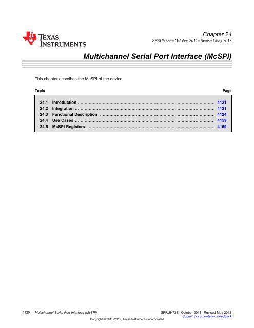
This device includes two instantiations of <strong>McSPI</strong>: SPI0 and SPI1. The <strong>McSPI</strong> module is a general-purpose<br />
receive/transmit master/slave controller that can interface with either up to four slave external devices or<br />
one single external master. Figure <strong>24</strong>-1 shows the example of a system with multiple external slave SPI<br />
compatible devices and Figure <strong>24</strong>-2 shows the example of a system with an external master.<br />
L4Peripheral<br />
Interconnect<br />
MPU Subsystem,<br />
PRU-ICSS<br />
EDMA<br />
PER_CLKOUTM2<br />
(192 MHz)<br />
PRCM<br />
/4<br />
L4Peripheral<br />
Interconnect<br />
MPU Subsystem,<br />
PRU-ICSS<br />
EDMA<br />
PER_CLKOUTM2<br />
(192 MHZ)<br />
PRCM<br />
/4<br />
SINTERRUPTN<br />
<strong>McSPI</strong>0<br />
TINT 34<br />
CH[1:0]SDMARREQN<br />
CH[1:0]SDMAWREQN<br />
PIRFFRET<br />
SPI_GCLK<br />
CH[3:2]SDMARREQN<br />
CH[3:2]SDMAWREQN<br />
CLKSPIREF<br />
<strong>McSPI</strong><br />
Pads<br />
SPICLK SPI_SCLK<br />
SPIDAT0 SPI_D0<br />
SPIDAT1<br />
SPI_D1<br />
SPIEN0 SPI_CS0n<br />
SPIEN1 SPI_CS1n<br />
SPIEN2<br />
SPIEN3<br />
Figure <strong>24</strong>-1. SPI Master Application<br />
SPI_GCLK<br />
SINTERRUPTN<br />
<strong>McSPI</strong>0<br />
CH[1:0]SDMARREQN<br />
CH[1:0]SDMAWREQN<br />
CH[3:2]SDMARREQN<br />
CH[3:2]SDMAWREQN<br />
PIRFFRET<br />
CLKSPIREF<br />
SPICLK<br />
SPIDAT0<br />
SPIDAT1<br />
SPIEN0<br />
SPIEN1<br />
SPIEN2<br />
SPIEN3<br />
Figure <strong>24</strong>-2. SPI Slave Application<br />
<strong>McSPI</strong><br />
Pads<br />
SPI_SCLK<br />
SPI_D0<br />
SPI_D1<br />
SPI_CS0n<br />
SPI_CS1n<br />
Slave SPI Devices<br />
SCLK<br />
MOSI<br />
MISO<br />
CSn<br />
SCLK<br />
MOSI<br />
MISO<br />
CSn<br />
Master SPI<br />
Device<br />
4122 <strong>Multichannel</strong> <strong>Serial</strong> <strong>Port</strong> <strong>Interface</strong> (<strong>McSPI</strong>) SPRUH73E–October 2011–Revised May 2012<br />
Submit Documentation Feedback<br />
Copyright © 2011–2012, Texas Instruments Incorporated<br />
CSn
www.ti.com Integration<br />
<strong>24</strong>.2.1 <strong>McSPI</strong> Connectivity Attributes<br />
The general connectivity attributes for the <strong>McSPI</strong> module are shown in Table <strong>24</strong>-2.<br />
Table <strong>24</strong>-2. <strong>McSPI</strong> Connectivity Attributes<br />
Attributes Type<br />
Power Domain Peripheral Domain<br />
Clock Domain PD_PER_L4LS_GCLK (<strong>Interface</strong>/OCP)<br />
PD_PER_SPI_GCLK (Func)<br />
Reset Signals PER_DOM_RST_N<br />
Idle/Wakeup Signals Smart Idle<br />
Interrupt Requests 1 interrupt to MPU subsystem and PRU-ICSS (<strong>McSPI</strong>0INT)<br />
1 interrupt to MPU subsystem only (<strong>McSPI</strong>1INT)<br />
DMA Requests 4 DMA requests per instance to EDMA<br />
• 1 RX request for CS0 (SPIREVT0)<br />
• 1 TX request for CS0 (SPIXEVT0)<br />
• 1 RX request for CS1 (SPIREVT1)<br />
• 1 TX request for CS1 (SPIXEVT1)<br />
Physical Address L4 Peripheral slave port<br />
<strong>24</strong>.2.2 <strong>McSPI</strong> Clock and Reset Management<br />
The SPI module clocks can be woken up in two manners: by the SPI module itself using the SWAKEUP<br />
signal (refer to the module functional spec for detailed conditions), or directly from an external SPI master<br />
device by detecting an active low level on its chip select input pin (CS0n) using a GPIO attached to that<br />
device pin. Neither of these methods is supported on the device.<br />
Table <strong>24</strong>-3. <strong>McSPI</strong> Clock Signals<br />
Clock Signal Max Freq Reference / Source Comments<br />
CLK 100 MHz CORE_CLKOUTM4 / 2 pd_per_l4ls_gclk<br />
<strong>Interface</strong> clock From PRCM<br />
CLKSPIREF 48 MHz PER_CLKOUTM2 / 4 pd_per_spi_gclk<br />
Functional clock From PRCM<br />
<strong>24</strong>.2.3 <strong>McSPI</strong> Pin List<br />
The <strong>McSPI</strong> interface pins are summarized in Table <strong>24</strong>-4.<br />
Table <strong>24</strong>-4. <strong>McSPI</strong> Pin List<br />
Pin Type Description<br />
SPIx_SCLK I/O SPI serial clock (output when master,<br />
input when slave)<br />
SPIx_D0 I/O Can be configured as either input or<br />
output (MOSI or MISO)<br />
SPIx_D1 I/O Can be configured as either input or<br />
output (MOSI or MISO)<br />
SPIx_CS0 I/O SPI chip select 0 output when master,<br />
input when slave (active low)<br />
SPIx_CS1 O SPI chip select 1 output when master,<br />
input when slave (active low)<br />
SPRUH73E–October 2011–Revised May 2012 <strong>Multichannel</strong> <strong>Serial</strong> <strong>Port</strong> <strong>Interface</strong> (<strong>McSPI</strong>)<br />
Submit Documentation Feedback<br />
Copyright © 2011–2012, Texas Instruments Incorporated<br />
4123
Functional Description www.ti.com<br />
<strong>24</strong>.3 Functional Description<br />
<strong>24</strong>.3.1 SPI Transmission<br />
This section describes the transmissions supported by <strong>McSPI</strong>. The SPI protocol is a synchronous protocol<br />
that allows a master device to initiate serial communication with a slave device. Data is exchanged<br />
between these devices. A slave select line (SPIEN) can be used to allow selection of an individual slave<br />
SPI device. Slave devices that are not selected do not interfere with SPI bus activities. Connected to<br />
multiple external devices, <strong>McSPI</strong> exchanges data with a single SPI device at a time through two main<br />
modes:<br />
• Two data pins interface mode. (See Section <strong>24</strong>.3.1.1)<br />
• Single data pin interface mode (recommended for half-duplex transmission). (See Section <strong>24</strong>.3.1.2)<br />
The flexibility of <strong>McSPI</strong> allows exchanging data with several formats through programmable parameters<br />
described in Section <strong>24</strong>.3.1.3.<br />
41<strong>24</strong> <strong>Multichannel</strong> <strong>Serial</strong> <strong>Port</strong> <strong>Interface</strong> (<strong>McSPI</strong>) SPRUH73E–October 2011–Revised May 2012<br />
Submit Documentation Feedback<br />
Copyright © 2011–2012, Texas Instruments Incorporated
www.ti.com Functional Description<br />
<strong>24</strong>.3.1.1 Two Data Pins <strong>Interface</strong> Mode<br />
The two data pins interface mode, allows a full duplex SPI transmission where data is transmitted (shifted<br />
out serially) and received (shifted in serially) simultaneously on separate data lines SPIDAT [0] and<br />
SPIDAT [1]. Data leaving the master exits on transmit serial data line also known as MOSI:<br />
MasterOutSlaveIn. Data leaving the slave exits on the receive data line also known as MISO:<br />
MasterInSlaveOut.<br />
<strong>McSPI</strong> has a unified SPI port control: SPIDAT [1:0] can be independently configured as receive or transmit<br />
lines. The user has the responsibility to program which data line to use and in which direction (receive or<br />
transmit), according to the external slave/master connection.<br />
The serial clock (SPICLK) synchronizes shifting and sampling of the information on the two serial data<br />
lines (SPIDAT [1:0]). Each time a bit is transferred out from the Master, one bit is transferred in from<br />
Slave.<br />
Figure <strong>24</strong>-3 shows an example of a full duplex system with a Master device on the left and a Slave device<br />
on the right. After 8 cycles of the serial clock SPICLK, the WordA has been transferred from the master to<br />
the slave. At the same time, the 8-bit WordB has been transferred from the slave to the master.<br />
When referring to the master device, the control block transmits the clock SPICLK and the enable signal<br />
SPIEN (optional, see Section <strong>24</strong>.5.1.7, <strong>McSPI</strong>_MODULECTRL).<br />
After 8<br />
Initial<br />
Transmitter Buffer<br />
Master<br />
Shift Register<br />
Control<br />
Receiver Register<br />
Master SPI Shift<br />
WordA<br />
<strong>24</strong>.3.1.2 Single Data Pin <strong>Interface</strong> Mode<br />
Figure <strong>24</strong>-3. SPI Full-Duplex Transmission<br />
SPIDAT[0]<br />
SPIDAT[1]<br />
SPICLK<br />
MOSI<br />
MISO<br />
SPIEN (Optional) Control<br />
WordB After 8<br />
Initial<br />
Transmitter Buffer<br />
Shift Register<br />
Slave SPI Shift Register<br />
WordB<br />
Slave<br />
Receiver Register<br />
RX Full?<br />
In single data pin interface mode, under software control, a single data line is used to alternatively transmit<br />
and receive data (Half duplex transmission).<br />
<strong>McSPI</strong> has a unified SPI port control: SPIDAT [1:0] can be independently configured as receive or transmit<br />
lines. The user has the responsibility to program which data line to use and in which direction (receive or<br />
transmit), according to the external slave/master connection.<br />
As for a full duplex transmission, the serial clock (SPICLK) synchronizes shifting and sampling of the<br />
information on the single serial data line.<br />
SPRUH73E–October 2011–Revised May 2012 <strong>Multichannel</strong> <strong>Serial</strong> <strong>Port</strong> <strong>Interface</strong> (<strong>McSPI</strong>)<br />
Submit Documentation Feedback<br />
Copyright © 2011–2012, Texas Instruments Incorporated<br />
4125
Functional Description www.ti.com<br />
<strong>24</strong>.3.1.2.1 Example With a Receive-Only Slave<br />
Figure <strong>24</strong>-4 shows a half duplex system with a Master device on the left and a receive-only Slave device<br />
on the right. Each time a bit is transferred out from the Master, one bit is transferred in the Slave. After 8<br />
cycles of the serial clock SPICLK, the 8-bit WordA has been transferred from the master to the slave.<br />
After 8<br />
After 8<br />
Figure <strong>24</strong>-4. SPI Half-Duplex Transmission (Receive-only Slave)<br />
Initial<br />
Transmitter Buffer<br />
Master<br />
Shift Register<br />
Control<br />
Receiver Register<br />
Master SPI Shift<br />
WordA<br />
WordB After 8<br />
<strong>24</strong>.3.1.2.2 Example With a Transmit-Only Slave<br />
Initial<br />
Transmitter Buffer<br />
Master<br />
Shift Register<br />
Control<br />
Receiver Register<br />
Master SPI Shift<br />
WordA<br />
SPIDAT<br />
(Single Line)<br />
SPICLK<br />
SPIEN (Optional) Control<br />
WordB After 8<br />
Initial<br />
Initial<br />
Shift Register<br />
Slave<br />
(Receive Only)<br />
Receiver Register<br />
Slave SPI Shift Register<br />
WordB<br />
WordA<br />
Figure <strong>24</strong>-5 shows a half duplex system with a Master device on the left and a transmit-only Slave device<br />
on the right. Each time a bit is transferred out from the Slave, one bit is transferred in the Master. After 8<br />
cycles of the serial clock SPICLK, the 8-bit WordA has been transferred from the slave to the master.<br />
Figure <strong>24</strong>-5. SPI Half-Duplex Transmission (Transmit-Only Slave)<br />
SPIDAT<br />
(Single Line)<br />
SPICLK<br />
SPIEN (Optional) Control<br />
Transmitter Buffer<br />
Shift Register<br />
Slave<br />
(Transmit Only)<br />
Slave SPI Shift Register<br />
WordB<br />
WordC<br />
4126 <strong>Multichannel</strong> <strong>Serial</strong> <strong>Port</strong> <strong>Interface</strong> (<strong>McSPI</strong>) SPRUH73E–October 2011–Revised May 2012<br />
Submit Documentation Feedback<br />
Copyright © 2011–2012, Texas Instruments Incorporated
www.ti.com Functional Description<br />
<strong>24</strong>.3.1.3 Transfer Formats<br />
This section describes the transfer formats supported by <strong>McSPI</strong>.<br />
The flexibility of <strong>McSPI</strong> allows setting the parameters of the SPI transfer:<br />
• SPI word length<br />
• SPI enable generation programmable<br />
• SPI enable assertion<br />
• SPI enable polarity<br />
• SPI clock frequency<br />
• SPI clock phase<br />
• SPI clock polarity<br />
The consistency between SPI word length, clock phase and clock polarity of the master SPI device and<br />
the communicating slave device remains under software responsibility.<br />
<strong>24</strong>.3.1.3.1 Programmable Word Length<br />
<strong>McSPI</strong> supports any SPI word from 4 to 32 bits long.<br />
The SPI word length can be changed between transmissions to allow a master device to communicate<br />
with peripheral slaves having different requirements.<br />
<strong>24</strong>.3.1.3.2 Programmable SPI Enable Generation<br />
<strong>McSPI</strong> is able to generate or not the SPI enable, if management of chip select is de-asserted a point to<br />
point connection is mandatory. Only a single master of slave device can be connected to the SPI bus.<br />
<strong>24</strong>.3.1.3.3 Programmable SPI Enable (SPIEN)<br />
The polarity of the SPIEN signals is programmable. SPIEN signals can be active high or low.<br />
The assertion of the SPIEN signals is programmable: SPIEN signals can be manually asserted or can be<br />
automatically asserted.<br />
Two consecutive words for two different slave devices may go along with active SPIEN signals with<br />
different polarity.<br />
<strong>24</strong>.3.1.3.4 Programmable SPI Clock (SPICLK)<br />
The phase and the polarity of the SPI serial clock are programmable when <strong>McSPI</strong> is a SPI master device<br />
or a SPI slave device. The baud rate of the SPI serial clock is programmable when <strong>McSPI</strong> is a SPI<br />
master.<br />
When <strong>McSPI</strong> is operating as a slave, the serial clock SPICLK is an input from the master.<br />
<strong>24</strong>.3.1.3.5 Bit Rate<br />
In Master Mode, an internal reference clock CLKSPIREF is used as an input of a programmable divider to<br />
generate bit rate of the serial clock SPICLK. Granularity of this clock divider can be changed.<br />
SPRUH73E–October 2011–Revised May 2012 <strong>Multichannel</strong> <strong>Serial</strong> <strong>Port</strong> <strong>Interface</strong> (<strong>McSPI</strong>)<br />
Submit Documentation Feedback<br />
Copyright © 2011–2012, Texas Instruments Incorporated<br />
4127
Functional Description www.ti.com<br />
<strong>24</strong>.3.1.3.6 Polarity and Phase<br />
<strong>McSPI</strong> supports four sub-modes of the SPI format transfer that depend on the polarity (POL) and the<br />
phase (PHA) of the SPI serial clock (SPICLK). Table <strong>24</strong>-5 and Figure <strong>24</strong>-6 show a summary of the four<br />
sub-modes. Software selects one of four combinations of serial clock phase and polarity.<br />
Two consecutive SPI words for two different slave devices may go along with active SPICLK signal with<br />
different phase and polarity.<br />
Table <strong>24</strong>-5. Phase and Polarity Combinations<br />
Polarity (POL) Phase (PHA) SPI Mode Comments<br />
0 0 mode0 SPICLK active high and sampling occurs on the rising edge.<br />
0 1 mode1 SPICLK active high and sampling occurs on the falling edge.<br />
1 0 mode2 SPICLK active low and sampling occurs on the falling edge.<br />
1 1 mode3 SPICLK active low and sampling occurs on the rising edge.<br />
Figure <strong>24</strong>-6. Phase and Polarity Combinations<br />
SPICLK (mode0)<br />
SPICLK (mode1)<br />
SPICLK (mode2)<br />
SPICLK (mode3)<br />
4128 <strong>Multichannel</strong> <strong>Serial</strong> <strong>Port</strong> <strong>Interface</strong> (<strong>McSPI</strong>) SPRUH73E–October 2011–Revised May 2012<br />
Submit Documentation Feedback<br />
Copyright © 2011–2012, Texas Instruments Incorporated<br />
Sampling<br />
tLead
www.ti.com Functional Description<br />
<strong>24</strong>.3.1.3.7 Transfer Format With PHA = 0<br />
This section describes the concept of a SPI transmission with the SPI mode0 and the SPI mode2.<br />
In the transfer format with PHA = 0, SPIEN is activated a half cycle of SPICLK ahead of the first SPICLK<br />
edge.<br />
In both master and slave modes, <strong>McSPI</strong> drives the data lines at the time of SPIEN is asserted.<br />
Each data frame is transmitted starting with the MSB. At the extremity of both SPI data lines, the first bit of<br />
SPI word is valid a half-cycle of SPICLK after the SPIEN assertion.<br />
Therefore, the first edge of the SPICLK line is used by the master to sample the first data bit sent by the<br />
slave. On the same edge, the first data bit sent by the master is sampled by the slave.<br />
On the next SPICLK edge, the received data bit is shifted into the shift register, and a new data bit is<br />
transmitted on the serial data line.<br />
This process continues for a total of pulses on the SPICLK line defined by the SPI word length<br />
programmed in the master device, with data being latched on odd numbered edges and shifted on even<br />
numbered edges.<br />
Figure <strong>24</strong>-7 is a timing diagram of a SPI transfer for the SPI mode0 and the SPI mode2, when <strong>McSPI</strong> is<br />
master or slave, with the frequency of SPICLK equals to the frequency of CLKSPIREF. It should not be<br />
used as a replacement for SPI timing information and requirements detailed in the data manual.<br />
When <strong>McSPI</strong> is in slave mode, if the SPIEN line is not de-asserted between successive transmissions<br />
then the content of the Transmitter register is not transmitted, instead the last received SPI word is<br />
transmitted.<br />
In master mode, the SPIEN line must be negated and reasserted between each successive SPI word.<br />
This is because the slave select pin freezes the data in its shift register and does not allow it to be altered<br />
if PHA bit equals 0.<br />
In 3-pin mode without using the SPIEN signal, the controller provides the same waveform but with SPIEN<br />
forced to low state. In slave mode SPIEN is useless<br />
SPICLK Edge Nr.<br />
SPICLK (POL=0)<br />
SPICLK (POL=1)<br />
Sample<br />
Data From the Master<br />
Data From the Slave<br />
Slave Select<br />
(SPIEN) (optional)<br />
Figure <strong>24</strong>-7. Full Duplex Single Transfer Format with PHA = 0<br />
Begin<br />
End<br />
1 2 3 4 5 6 7 8 9 10 11 12 13 14 15 16<br />
MSB Bit6 Bit5 Bit4 Bit3 Bit2 Bit1 LSB<br />
MSB Bit6 Bit5 Bit4 Bit3 Bit2 Bit1 LSB<br />
t LEAD<br />
Transfer<br />
SPRUH73E–October 2011–Revised May 2012 <strong>Multichannel</strong> <strong>Serial</strong> <strong>Port</strong> <strong>Interface</strong> (<strong>McSPI</strong>)<br />
Submit Documentation Feedback<br />
Copyright © 2011–2012, Texas Instruments Incorporated<br />
t LAG<br />
4129
Functional Description www.ti.com<br />
<strong>24</strong>.3.1.3.8 Transfer Format With PHA = 1<br />
This section describes SPI full duplex transmission with the SPI mode1 and the SPI mode3.<br />
In the transfer format with PHA = 1, SPIEN is activated a delay (t Lead) ahead of the first SPICLK edge.<br />
In both master and slave modes, <strong>McSPI</strong> drives the data lines on the first SPICLK edge.<br />
Each data frame is transmitted starting with the MSB. At the extremity of both SPI data lines, the first bit of<br />
SPI word is valid on the next SPICLK edge, a half-cycle later of SPICLK. It is the sampling edge for both<br />
the master and slave.<br />
When the third edge occurs, the received data bit is shifted into the shift register. The next data bit of the<br />
master is provided to the serial input pin of the slave.<br />
This process continues for a total of pulses on the SPICLK line defined by the word length programmed in<br />
the master device, with data being latched on even numbered edges and shifted on odd numbered edges.<br />
Figure <strong>24</strong>-8 is a timing diagram of a SPI transfer for the SPI mode1 and the SPI mode3, when <strong>McSPI</strong> is<br />
master or slave, with the frequency of SPICLK equals to the frequency of CLKSPIREF. It should not be<br />
used as a replacement for SPI timing information and requirements detailed in the data manual.<br />
The SPIEN line may remain active between successive transfers. In 3-pin mode without using the SPIEN<br />
signal, the controller provides the same waveform but with SPIEN forced to low state. In slave mode<br />
SPIEN is useless.<br />
SPICLK Edge Nr.<br />
SPICLK (POL=0)<br />
SPICLK (POL=1)<br />
Sample<br />
Data From the Master<br />
Data From the Slave<br />
Slave Select<br />
(SPIEN) (optional)<br />
Figure <strong>24</strong>-8. Full Duplex Single Transfer Format With PHA = 1<br />
Begin<br />
End<br />
1 2 3 4 5 6 7 8 9 10 11 12 13 14 15 16<br />
MSB Bit6 Bit5 Bit4 Bit3 Bit2 Bit1 LSB<br />
MSB Bit6 Bit5 Bit4 Bit3 Bit2 Bit1 LSB<br />
t LEAD<br />
Transfer<br />
4130 <strong>Multichannel</strong> <strong>Serial</strong> <strong>Port</strong> <strong>Interface</strong> (<strong>McSPI</strong>) SPRUH73E–October 2011–Revised May 2012<br />
Submit Documentation Feedback<br />
Copyright © 2011–2012, Texas Instruments Incorporated<br />
t LAG
www.ti.com Functional Description<br />
<strong>24</strong>.3.2 Master Mode<br />
<strong>McSPI</strong> is in master mode when the bit MS of the register MCSPI_MODULCTRL is cleared.<br />
In master mode <strong>McSPI</strong> supports multi-channel communication with up to 4 independent SPI<br />
communication channel contexts. <strong>McSPI</strong> initiates a data transfer on the data lines (SPIDAT [1;0]) and<br />
generates clock (SPICLK) and control signals (SPIEN) to a single SPI slave device at a time.<br />
<strong>24</strong>.3.2.1 Dedicated Resources Per Channel<br />
In the following sections, the letter “I” indicates the channel number that can be 0, 1, 2 or 3. Each channel<br />
has the following dedicated resources:<br />
• Its own channel enable, programmable with the bit EN of the register MCSPI_CH(I)CTRL. Disabling<br />
the channel, outside data word transmission, remains under user responsibility.<br />
• Its own transmitter register MCSPI_TX on top of the common shift register. If the transmitter register is<br />
empty, the status bit TXS of the register MCSPI_CH(I)STAT is set.<br />
• Its own receiver register MCSPI_RX on top of the common shift register. If the receiver register is full,<br />
the status bit RXS of the register MCSPI_CH(I)STAT is set.<br />
• A fixed SPI ENABLE line allocation (SPIEN[i] port for channel “I”), SPI enable management is optional.<br />
• Its own communication configuration with the following parameters via the register (I)CONF<br />
– Transmit/Receive modes, programmable with the bit TRM.<br />
– <strong>Interface</strong> mode (Two data pins or Single data pin) and data pins assignment, both programmable<br />
with the bits IS and DPE.<br />
– SPI word length, programmable with the bits WL.<br />
– SPIEN polarity, programmable with the bit EPOL.<br />
– SPIEN kept active between words, programmable with the bit FORCE.<br />
– Turbo mode, programmable with the bit TURBO.<br />
– SPICLK frequency, programmable with the bit CLKD, the granularity of clock division can be<br />
changed using CLKG bit, the clock ratio is then concatenated with MCSPI_CHCTRL[EXTCLK]<br />
value.<br />
– SPICLK polarity, programmable with the bit POL<br />
– SPICLK phase, programmable with the bit PHA.<br />
– Start bit polarity, programmable with the bit SBPOL<br />
– Use a FIFO Buffer or not (see the following note), programmable with FFER and FFEW, depending<br />
on transfer mode, (MCSPI_CH(I)CONF[TRM]).<br />
• Two DMA requests events, read and write, to synchronize read/write accesses of the DMA controller<br />
with the activity of <strong>McSPI</strong>. The DMA requests are enabled with the bits DMAR and DMAW.<br />
• Three interrupts events<br />
Note: When more than one channel has an FIFO enable bit field (FFER or FFEW) set, the FIFO will not<br />
be used on any channel. Software must ensure that only one enabled channel is configured to use the<br />
FIFO buffer.<br />
The transfers will use the latest loaded parameters of the register MCSPI_CH(I)CONF.<br />
The configuration parameters SPIEN polarity, Turbo mode, SPICLK phase and SPICLK polarity can be<br />
loaded in the MCSPI_CH(I)CONF register only when the channel is disabled. The user has the<br />
responsibility to change the other parameters of the MCSPI_CH(I)CONF register when no transfer occurs<br />
on the SPI interface.<br />
SPRUH73E–October 2011–Revised May 2012 <strong>Multichannel</strong> <strong>Serial</strong> <strong>Port</strong> <strong>Interface</strong> (<strong>McSPI</strong>)<br />
Submit Documentation Feedback<br />
Copyright © 2011–2012, Texas Instruments Incorporated<br />
4131
Functional Description www.ti.com<br />
<strong>24</strong>.3.2.2 Interrupt Events in Master Mode<br />
In master mode, the interrupt events related to the transmitter register state are TX_empty and<br />
TX_underflow. The interrupt event related to the receiver register state is RX_full.<br />
<strong>24</strong>.3.2.2.1 TX_empty<br />
The event TX_empty is activated when a channel is enabled and its transmitter register becomes empty<br />
(transient event). Enabling channel automatically raises this event, except for the Master receive only<br />
mode. (See Section <strong>24</strong>.3.2.5). When the FIFO buffer is enabled (MCSPI_CH(I)CONF[FFEW] set to 1), the<br />
TX_empty is asserted as soon as there is enough space in the buffer to write a number of bytes defined<br />
by MCSPI_XFERLEVEL[AEL].<br />
Transmitter register must be loaded to remove the source of the interrupt and the TX_empty interrupt<br />
status bit must be cleared for interrupt line de-assertion (if event enabled as interrupt source) . (See<br />
Section <strong>24</strong>.3.4).<br />
When FIFO is enabled, no new TX_empty event will be asserted as soon as CPU has not performed the<br />
number of write into transmitter register defined by MCSPI_XFERLEVEL[AEL]. It is the responsibility of<br />
CPU to perform the right number of writes.<br />
<strong>24</strong>.3.2.2.2 TX_underflow<br />
The event TX_underflow is activated when the channel is enabled and if the transmitter register or FIFO is<br />
empty (not updated with new data) at the time of shift register assignment.<br />
The TX_underflow is a harmless warning in master mode.<br />
To avoid having TX_underflow event at the beginning of a transmission, the event TX_underflow is not<br />
activated when no data has been loaded into the transmitter register since channel has been enabled.<br />
To avoid having a TX_underflow event, the Transmit Register (MCSPI_TX(i)) should be loaded as<br />
infrequently as possible.<br />
TX_underflow interrupt status bit must be cleared for interrupt line de-assertion (if event enable as<br />
interrupt source).<br />
Note: When more than one channel has an FIFO enable bit field (FFER or FFEW) set, the FIFO will not<br />
be used on any channel. Software must ensure that only one enabled channel is configured to use the<br />
FIFO buffer.<br />
<strong>24</strong>.3.2.2.3 RX_ full<br />
The event RX_full is activated when channel is enabled and receiver register becomes filled (transient<br />
event). When FIFO buffer is enabled (MCSPI_CH(I)CONF[FFER] set to 1), the RX_full is asserted when<br />
the number of bytes in the buffer equals the level defined by MCSPI_XFERLEVEL[AFL].<br />
Receiver register must be read to remove source of interrupt and RX_full interrupt status bit must be<br />
cleared for interrupt line de-assertion (if event enabled as interrupt source).<br />
When the FIFO is enabled, no new RX_FULL event will be asserted once the CPU has read the number<br />
of bytes defined by MCSPI_XFERLEVEL[AFL]. It is the responsibility of the CPU to perform the correct<br />
number of read operations.<br />
<strong>24</strong>.3.2.2.4 End of Word Count<br />
The event end of word (EOW) count is activated when channel is enabled and configured to use the builtin<br />
FIFO. This interrupt is raised when the controller had performed the number of transfer defined in<br />
MCSPI_XFERLEVEL[WCNT] register. If the value was programmed to 0000h, the counter is not enabled<br />
and this interrupt is not generated.<br />
The EOW count interrupt also indicates that the SPI transfer has halted on the channel using the FIFO<br />
buffer.<br />
The EOW interrupt status bit must be cleared for interrupt line de-assertion (if event enable as interrupt<br />
source).<br />
4132 <strong>Multichannel</strong> <strong>Serial</strong> <strong>Port</strong> <strong>Interface</strong> (<strong>McSPI</strong>) SPRUH73E–October 2011–Revised May 2012<br />
Submit Documentation Feedback<br />
Copyright © 2011–2012, Texas Instruments Incorporated
www.ti.com Functional Description<br />
<strong>24</strong>.3.2.3 Master Transmit and Receive Mode<br />
This mode is programmable per channel (bit TRM of register MCSPI_CH(I)CONF).<br />
The channel access to the shift registers, for transmission/reception, is based on its transmitter and<br />
receiver register state and round robin arbitration.<br />
The channel that meets the rules below is included in the round robin list of already active channels<br />
scheduled for transmission and/or reception. The arbiter skips the channel that does not meet the rules<br />
and search for the next following enabled channel, in rotation.<br />
Rule 1: Only enabled channels (bit EN of the register MCSPI_CH(I)CTRL), can be scheduled for<br />
transmission and/or reception.<br />
Rule 2: An enabled channel can be scheduled if its transmitter register is not empty (bit TXS of the<br />
register MCSPI_CH(I)STAT) or its FIFO is not empty when the buffer is used for the corresponding<br />
channel (bit FFE of the register MCSPI_CH(I)STAT) at the time of shift register assignment. If the<br />
transmitter register or FIFO is empty, at the time of shift register assignment, the event TX_underflow is<br />
activated and the next enabled channel with new data to transmit is scheduled. (See also transmit only<br />
mode).<br />
Rule 3: An enabled channel can be scheduled if its receive register is not full (bit RXS of the register<br />
MCSPI_CH(I)STAT)) or its FIFO is not full when the buffer is used for the corresponding channel (bit FFF<br />
of the register MCSPI_CH(I)STAT) at the time of shift register assignment. (See also receive only mode).<br />
Therefore the receiver register of FIFO cannot be overwritten. The RX_overflow bit, in the<br />
MCSPI_IRQSTATUS register is never set in this mode.<br />
On completion of SPI word transfer (bit EOT of the register MCSPI_CH(I)STAT is set) the updated<br />
transmitter register for the next scheduled channel is loaded into the shift register. This bit is meaningless<br />
when using the Buffer for this channel. The serialization (transmit and receive) starts according to the<br />
channel communication configuration. On serialization completion the received data is transferred to the<br />
channel receive register.<br />
The built-in FIFO is available in this mode and if configured in one data direction, transmit or receive, then<br />
the FIFO is seen as a unique FFNBYTE bytes buffer. If configured in both data directions, transmit and<br />
receive, then the FIFO is split into two separate FFNBYTE/2 bytes buffer with their own address space<br />
management. In this last case, the definition of AEL and AFL levels is based on FFNBYTE/2 bytes and is<br />
under CPU responsibility.<br />
<strong>24</strong>.3.2.4 Master Transmit-Only Mode<br />
This mode eliminates the need for the CPU to read the receiver register (minimizing data movement)<br />
when only transmission is meaningful.<br />
The master transmit only mode is programmable per channel (bits TRM of the register<br />
MCSPI_CH(I)CONF).<br />
In master transmit only mode, transmission starts after data is loaded into the transmitter register.<br />
Rule 1 and Rule 2, defined above, are applicable in this mode.<br />
Rule 3, defined above, is not applicable: In master transmit only mode, the receiver register or FIFO state<br />
“full” does not prevent transmission, and the receiver register is always overwritten with the new SPI word.<br />
This event in the receiver register is not significant when only transmission is meaningful. So, the<br />
RX_overflow bit, in the MCSPI_IRQSTATUS register is never set in this mode.<br />
The <strong>McSPI</strong> module automatically disables the RX_full interrupt status. The corresponding interrupt request<br />
and DMA Read request are not generated in master transmit only mode.<br />
The status of the serialization completion is given by the bit EOT of the register MCSPI_CH(I)STAT. This<br />
bit is meaningless when using the Buffer for this channel.<br />
The built-in FIFO is available in this mode and can be configured with FFEW bit field in the<br />
MCSPI_CH(I)CONF register, then the FIFO is seen as a unique FFNBYTE bytes buffer.<br />
SPRUH73E–October 2011–Revised May 2012 <strong>Multichannel</strong> <strong>Serial</strong> <strong>Port</strong> <strong>Interface</strong> (<strong>McSPI</strong>)<br />
Submit Documentation Feedback<br />
Copyright © 2011–2012, Texas Instruments Incorporated<br />
4133
Functional Description www.ti.com<br />
<strong>24</strong>.3.2.5 Master Receive-Only Mode<br />
This mode eliminates the need for the CPU to refill the transmitter register (minimizing data movement)<br />
when only reception is meaningful.<br />
The master receive mode is programmable per channel (bits TRM of the register MCSPI_CH(I)CONF).<br />
The master receive only mode enables channel scheduling only on empty state of the receiver register.<br />
Rule 1 and Rule 3, defined above, are applicable in this mode.<br />
Rule 2, defined above, is not applicable: In master receive only mode, after the first loading of the<br />
transmitter register of the enabled channel, the transmitter register state is maintained as full. The content<br />
of the transmitter register is always loaded into the shift register, at the time of shift register assignment.<br />
So, after the first loading of the transmitter register, the bits TX_empty and TX_underflow, in the<br />
MCSPI_IRQSTATUS register are never set in this mode.<br />
The status of the serialization completion is given by the bit EOT of the register MCSPI_CH(I)STAT. The<br />
bit RX_full in the MCSPI_IRQSTATUS register is set when a received data is loaded from the shift register<br />
to the receiver register. This bit is meaningless when using the Buffer for this channel.<br />
The built-in FIFO is available in this mode and can be configured with FFER bit field in the<br />
MCSPI_CH(I)CONF register, then the FIFO is seen as a unique FFNBYTE byte buffer.<br />
<strong>24</strong>.3.2.6 Single-Channel Master Mode<br />
When the SPI is configured as a master device with a single enabled channel, the assertion of the<br />
SPIM_CSX signal can be controlled in two different ways:<br />
• In 3 pin mode : MCSPI_MODULCTRL[1] PIN34 and MCSPI_MODULCTRL[0] SINGLE bit are set to 1,<br />
the controller transmit SPI word as soon as transmit register or FIFO is not empty.<br />
• In 4 pin mode : MCSPI_MODULCTRL[1] PIN34 bit is cleared to 0 and MCSPI_MODULCTRL[0]<br />
SINGLE bit is set to 1, SPIEN assertion/deassertion controlled by Software. (See Section <strong>24</strong>.3.2.6.1)<br />
using the MCSPI_CHxCONF[20] FORCE bit.<br />
<strong>24</strong>.3.2.6.1 Programming Tips When Switching to Another Channel<br />
When a single channel is enabled and data transfer is ongoing:<br />
• Wait for completion of the SPI word transfer (bit EOT of the register MCSPI_CH(I)STAT is set) before<br />
disabling the current channel and enabling a different channel.<br />
• Disable the current channel first, and then enable the other channel.<br />
<strong>24</strong>.3.2.6.2 Keep SPIEN Active Mode (Force SPIEN)<br />
Continuous transfers are manually allowed by keeping the SPIEN signal active for successive SPI words<br />
transfer. Several sequences (configuration/enable/disable of the channel) can be run without deactivating<br />
the SPIEN line. This mode is supported by all channels and any master sequence can be used (transmitreceive,<br />
transmit-only, receive-only).<br />
Keeping the SPIEN active mode is supported when:<br />
• A single channel is used (bit MCSPI_MODULCTRL[Single] is set to 1).<br />
• Transfer parameters of the transfer are loaded in the configuration register (MCSPI_CH(I)CONF) in the<br />
appropriate channel.<br />
The state of the SPIEN signal is programmable.<br />
– Writing 1 into the bit FORCE of the register MCSPI_CH(I)CONF drives high the SPIEN line when<br />
MCSPI_CHCONF(I)[EPOL] is set to zero, and drives it low when MCSPI_CHCONF(I)[EPOL] is set.<br />
– Writing 0 into the bit FORCE of the register MCSPI_CH(I)CONF drives low the SPIEN line when<br />
MCSPI_CHCONF(I)[EPOL] is set to zero, and drives it high when MCSPI_CHCONF(I)[EPOL] is<br />
set.<br />
• A single channel is enabled (MCSPI_CH(I)CTRL[En] set to 1) . The first enabled channel activates the<br />
SPIEN line.<br />
4134 <strong>Multichannel</strong> <strong>Serial</strong> <strong>Port</strong> <strong>Interface</strong> (<strong>McSPI</strong>) SPRUH73E–October 2011–Revised May 2012<br />
Submit Documentation Feedback<br />
Copyright © 2011–2012, Texas Instruments Incorporated
www.ti.com Functional Description<br />
Once the channel is enabled, the SPIEN signal is activated with the programmed polarity.<br />
As in multi-channel master mode, the start of the transfer depends on the status of the transmitter register,<br />
the status of the receiver register and the mode defined by the bits TRM in the configuration register<br />
(transmit only, receive only or transmit and receive) of the enabled channel.<br />
The status of the serialization completion of each SPI word is given by the bit EOT of the register<br />
MCSPI_CH(I)STAT. The bit RX_full in the MCSPI_IRQSTATUS register is set when a received data is<br />
loaded from the shift register to the receiver register.<br />
A change in the configuration parameters is propagated directly on the SPI interface. If the SPIEN signal<br />
is activated the user must insure that the configuration is changed only between SPI words, in order to<br />
avoid corrupting the current transfer.<br />
NOTE: The SPIEN polarity, the SPICLK phase and SPICLK polarity must not be modified when the<br />
SPIEN signal is activated. The Transmit/Receive mode, programmable with the bit TRM can<br />
be modified only when the channel is disabled. The channel can be disabled and enabled<br />
while the SPIEN signal is activated.<br />
The delay between SPI words that requires the connected SPI slave device to switch from one<br />
configuration (Transmit only for instance) to another (receive only for instance) must be handled under<br />
software responsibility.<br />
At the end of the last SPI word, the channel must be deactivated (MCSPI_CH(I)CTRL[En] is cleared to 0)<br />
and the SPIEN can be forced to its inactive state (MCSPI_CH(I)CONF[Force]).<br />
Figure <strong>24</strong>-9 and Figure <strong>24</strong>-10 show successive transfers with SPIEN kept active low with a different<br />
configuration for each SPI word in respectively single data pin interface mode and two data pins interface<br />
mode. The arrows indicate when the channel is disabled before a change in the configuration parameters<br />
and enabled again.<br />
Figure <strong>24</strong>-9. Continuous Transfers With SPIEN Maintained Active (Single-Data-Pin <strong>Interface</strong> Mode)<br />
SPIEN<br />
SPIDAT[0] Word Word Word<br />
SPICLK<br />
Figure <strong>24</strong>-10. Continuous Transfers With SPIEN Maintained Active (Dual-Data-Pin <strong>Interface</strong> Mode)<br />
SPIEN<br />
SPIDAT[0] Word Word<br />
SPIDAT[1]<br />
SPICLK<br />
Word<br />
SPRUH73E–October 2011–Revised May 2012 <strong>Multichannel</strong> <strong>Serial</strong> <strong>Port</strong> <strong>Interface</strong> (<strong>McSPI</strong>)<br />
Submit Documentation Feedback<br />
Copyright © 2011–2012, Texas Instruments Incorporated<br />
4135
Functional Description www.ti.com<br />
NOTE: The turbo mode is also supported for the Keep SPIEN active mode when the following<br />
conditions are met:<br />
• A single channel will be explicitly used (bit MCSPI_MODULCTRL[Single] is set to 1).<br />
• The turbo mode is enabled in the configuration of the channel (bit Turbo of the register<br />
(i)CONF).<br />
<strong>24</strong>.3.2.6.3 Turbo Mode<br />
The purpose of the Turbo mode is to improve the throughput of the SPI interface when a single channel is<br />
enabled, by allowing transfers until the shift register and the receiver register are full.<br />
This mode is programmable per channel (bit Turbo of the register (I)CONF). When several channels are<br />
enabled, the bit Turbo of the registers MCSPI_CH(I)CONF has no effect, and the channel access to the<br />
shift registers remains as described in Section <strong>24</strong>.3.2.3.<br />
In Turbo mode, Rule 1 and Rule 2 defined in Section <strong>24</strong>.3.2.3 are applicable but Rule 3 is not applicable.<br />
An enabled channel can be scheduled if its receive register is full (bit RXS of the register<br />
MCSPI_CH(I)STAT) at the time of shift register assignment until the shift register is full.<br />
The receiver register cannot be overwritten in turbo mode. In consequence the RX_overflow bit, in<br />
MCSPI_IRQSTATUS register is never set in this mode.<br />
<strong>24</strong>.3.2.7 Start Bit Mode<br />
The purpose of the start bit mode is to add an extended bit before the SPI word transmission specified by<br />
word length WL. This feature is only available in master mode.<br />
This mode is programmable per channel (bit Start bit enable SBE of the register MCSPI_CH(I)CONF).<br />
The polarity of the extended bit is programmable per channel and it indicates whether the next SPI word<br />
must be handled as a command when SBPOL is cleared to 0 or as a data or a parameter when SBPOL is<br />
set to 1. Moreover start bit polarity SBPOL can be changed dynamically during start bit mode transfer<br />
without disabling the channel for reconfiguration, in this case you have the responsibility to configure the<br />
SBPOL bit before writing the SPI word to be transmitted in TX register.<br />
The start bit mode could be used at the same time as turbo mode and/or manual chip select mode. In this<br />
case only one channel could be used, no round-robin arbitration is possible.<br />
4136 <strong>Multichannel</strong> <strong>Serial</strong> <strong>Port</strong> <strong>Interface</strong> (<strong>McSPI</strong>) SPRUH73E–October 2011–Revised May 2012<br />
Submit Documentation Feedback<br />
Copyright © 2011–2012, Texas Instruments Incorporated
www.ti.com Functional Description<br />
SPICLK Edge Nr.<br />
SPICLK (POL=0)<br />
SPICLK (POL=1)<br />
Sample<br />
Data From the Master<br />
Data From the Slave<br />
Slave Select<br />
(SPIEN) (optional)<br />
Figure <strong>24</strong>-11. Extended SPI Transfer With Start Bit PHA = 1<br />
t Lead<br />
Begin Transfer<br />
End<br />
1 2 3 4 5 6 7 8 9 10 11 12 13 14 15 16 17 18<br />
D/CX MSB Bit6 Bit5 Bit4 Bit3 Bit2 Bit1 LSB<br />
D/CX MSB Bit6 Bit5 Bit4 Bit3 Bit2 Bit1 LSB<br />
SPRUH73E–October 2011–Revised May 2012 <strong>Multichannel</strong> <strong>Serial</strong> <strong>Port</strong> <strong>Interface</strong> (<strong>McSPI</strong>)<br />
Submit Documentation Feedback<br />
Copyright © 2011–2012, Texas Instruments Incorporated<br />
4137
Functional Description www.ti.com<br />
<strong>24</strong>.3.2.8 Chip-Select Timing Control<br />
The chip select timing control is only available in master mode with automatic chip select generation<br />
(FORCE bit field is cleared to 0), to add a programmable delay between chip select assertion and first<br />
clock edge or chip select removal and last clock edge. The option is available only in 4 pin mode<br />
MCSPI_MODULCTRL[1] PIN34 is cleared to 0.<br />
This mode is programmable per channel (bit TCS of the register MCSPI_CH(I)CONF). Figure <strong>24</strong>-12<br />
shows the chip-select SPIEN timing control.<br />
SPI Shift Clock<br />
(Module Generated<br />
Internal Clock)<br />
SPICLKO<br />
(POL=1)<br />
SPICLKO<br />
(POL=0)<br />
SPIENO<br />
Figure <strong>24</strong>-12. Chip-Select SPIEN Timing Controls<br />
TCS = 0.5<br />
TCS = 1.5<br />
TCS = 2.5<br />
TCS = 3.5<br />
TCS = 0.5<br />
TCS = 1.5<br />
TCS = 2.5<br />
TCS = 3.5<br />
NOTE: Because of the design implementation for transfers using a clock divider ratio set to 1 (clock<br />
bypassed), a half cycle must be added to the value between chip-select assertion and the<br />
first clock edge with PHA = 1 or between chip-select removal and the last clock edge with<br />
PHA = 0.<br />
With an odd clock divider ratio which occurs when granularity is one clock cycle, that means that<br />
MCSPI_CH(I)CONF[CLKG] is set to 1 and MCSPI_CH(I)CONF[CLKD] has an even value, the clock duty<br />
cycle is not 50%, then one of the high level or low level duration is selected to be added to TCS delay.<br />
Table <strong>24</strong>-6 summarizes all delays between chip select and first (setup) or last (hold) clock edge.<br />
In 3-pin mode this option is useless, the chip select SPIEN is forced to low state.<br />
Table <strong>24</strong>-6. Chip Select ↔ Clock Edge Delay Depending on Configuration<br />
Clock Ratio Fratio Clock Chip Select ↔ Clock Edge Delay<br />
Phase<br />
PHA<br />
Setup Hold<br />
1 0 T_ref × (TCS + ½) T_ref × (TCS + 1)<br />
1 T_ref × (TCS + 1) T_ref × (TCS + ½)<br />
Even ≥ 2 x T_ref × F ratio × (TCS + ½) T_ref × F ratio × (TCS + ½)<br />
Odd ≥ 3 (only with 0 T_ref × [{Fratio × TCS) + (Fratio + ½)] T_ref × [{Fratio × TCS) + (Fratio + ½)]<br />
MCSPI_CH(I)CONF[CLK<br />
1 T_ref × [{Fratio × TCS) + (Fratio - ½)] T_ref × [{Fratio × TCS) + (Fratio - ½)]<br />
G] set to 1<br />
T_ref = CLKSPIREF period in ns. F ratio = SPI clock division ratio<br />
The clock divider ratio depends on divider granularity MCSPI_CH(I)CONF[CLKG]:<br />
• MCSPI_CH(I)CONF[CLKG] = 0 : granularity is power of two.<br />
F ratio = 2 MCSPI_CH(I)CONF[CLKD]<br />
• MCSPI_CH(I)CONF[CLKG] = 0 : granularity is power of two.<br />
4138 <strong>Multichannel</strong> <strong>Serial</strong> <strong>Port</strong> <strong>Interface</strong> (<strong>McSPI</strong>) SPRUH73E–October 2011–Revised May 2012<br />
Submit Documentation Feedback<br />
Copyright © 2011–2012, Texas Instruments Incorporated
www.ti.com Functional Description<br />
F ratio = MCSPI_CH(I)CNTRL[EXTCLK].MCSPI_CH(I)CONF[CLKD] + 1<br />
SPRUH73E–October 2011–Revised May 2012 <strong>Multichannel</strong> <strong>Serial</strong> <strong>Port</strong> <strong>Interface</strong> (<strong>McSPI</strong>)<br />
Submit Documentation Feedback<br />
Copyright © 2011–2012, Texas Instruments Incorporated<br />
4139
Functional Description www.ti.com<br />
<strong>24</strong>.3.2.9 Clock Ratio Granularity<br />
By default the clock division ratio is defined by the register MCSPI_CH(I)CONF[CLKD] with power of two<br />
granularity leading to a clock division in range 1 to 32768, in this case the duty cycle is always 50%. With<br />
bit MCSPI_CH(I)CONF[CLKG] the clock division granularity can be changed to one clock cycle, in that<br />
case the register MCSPI_CH(I)CTRL[EXTCLK] is concatenated with MCSPI_CH(I)CONF[CLKD] to give a<br />
12-bit width division ratio in range 1 to 4096.<br />
When granularity is one clock cycle (MCSPI_CH(I)CONF[CLKG] set to 1), for odd value of clock ratio the<br />
clock duty cycle is kept to 50-50 using falling edge of clock reference CLKSPIREF.<br />
Table <strong>24</strong>-7. CLKSPIO High/Low Time Computation<br />
Clock Ratio F ratio CLKSPIO High Time CLKSPIO Low Time<br />
1 T high_ref T low_ref<br />
Even ≥ 2 t_ref × (F ratio/2) t_ref × (F ratio/2)<br />
Odd ≥ 3 t_ref × (F ratio/2) t_ref × (F ratio/2)<br />
T_ref = CLKSPIREF period in ns. T high_ref = CLKSPIREF high Time period in ns. T low_ref = CLKSPIREF<br />
low Time period in ns. F ratio = SPI clock division ratio<br />
F ratio = MCSPI_CH(I)CTRL[EXTCLK].MCSPI_CH(I)CONF[CLKD] + 1<br />
For odd ratio value the duty cycle is calculated as below:<br />
Duty_cycle = ½<br />
Granularity examples: With a clock source frequency of 48 MHz:<br />
Table <strong>24</strong>-8. Clock Granularity Examples<br />
MCSPI_CH MCSPI_CH MCSPI_CH MCSPI_CH MCSPI_CH<br />
(I)CTRL (I)CONF (I)CONF (I)CONF (I)CONF<br />
Thigh Tlow Tperiod Duty Fout<br />
EXTCLK CLKD CLKG Fratio PHA POL (ns) (ns) (ns) Cycle (MHz)<br />
X 0 0 1 X X 10.4 10.4 20.8 50-50 48<br />
X 1 0 2 X X 20.8 20.8 41.6 50-50 <strong>24</strong><br />
X 2 0 4 X X 41.6 41.6 83.2 50-50 12<br />
X 3 0 8 X X 83.2 83.2 166.4 50-50 6<br />
0 0 1 1 X X 10.4 10.4 20.8 50-50 48<br />
0 1 1 2 X X 20.8 20.8 41.6 50-50 <strong>24</strong><br />
0 2 1 3 1 0 31,2 31,2 62.4 50-50 16<br />
0 2 1 3 1 1 31,2 31,2 62.4 50-50 16<br />
0 3 1 4 X X 41.6 41.6 83.2 50-50 12<br />
5 0 1 81 1 0 842,4 842,4 1684.8 50-50 0.592<br />
5 7 1 88 X X 915.2 915.2 1830.4 50-50 0.545<br />
4140 <strong>Multichannel</strong> <strong>Serial</strong> <strong>Port</strong> <strong>Interface</strong> (<strong>McSPI</strong>) SPRUH73E–October 2011–Revised May 2012<br />
Submit Documentation Feedback<br />
Copyright © 2011–2012, Texas Instruments Incorporated
www.ti.com Functional Description<br />
<strong>24</strong>.3.2.10 FIFO Buffer Management (Optional USEFIFO = 1)<br />
The <strong>McSPI</strong> controller has a built-in FFNBYTE bytes buffer in order to unload DMA or interrupt handler and<br />
improve data throughput. The use of this buffer is optional and depends on a generic parameter<br />
USEFIFO. The FIFO is enabled when it is set to 1. Allowed FIFO depth up to 64 bytes is supported and is<br />
defined by generic parameter FFNBYTE. When the FIFO is not enabled, writes to registers<br />
MCSPI_XFERLEVEL, MCSPI_CH(I)CONF[FFER] and MCSPI_CH(I)CONF[FFEW] have no functional<br />
effect, nevertheless read back is allowed to check written value.<br />
This buffer can be used by only one channel and is selected by setting MCSPI_CH(I)CONF[FFER] and/or<br />
MCSPI_CH(I)CONF[FFEW] to 1.<br />
If several channels are selected and several FIFO enable bit fields set to 1, the controller forces the buffer<br />
to be disabled for all channels. It is the responsibility of the driver to enable the buffer for only one<br />
channel.<br />
The buffer can be used in the modes defined below:<br />
• Master or Slave mode.<br />
• Transmit only, Receive only or Transmit/Receive mode.<br />
• Single channel or turbo mode, or in normal round robin mode. In round robin mode the buffer is used<br />
by only one channel.<br />
• All word length MCSPI_CH(I)CONF[WL] are supported.<br />
Two levels AEL and AFL located in MCSPI_XFERLEVEL register rule the buffer management. The<br />
granularity of these levels is one byte, then it is not aligned with SPI word length. It is the responsibility of<br />
the driver to set these values as a multiple of SPI word length defined in MCSPI_CH(I)CONF[WL]. The<br />
number of byte written in the FIFO depends on word length (see Table <strong>24</strong>-9).<br />
Table <strong>24</strong>-9. FIFO Writes, Word Length Relationship<br />
SPI Word Length WL<br />
3 ≤ WL ≤ 7 8 ≤ WL ≤ 15 16 ≤ WL ≤ 31<br />
Number of byte written in the FIFO 1 byte 2 bytes 4 byte<br />
<strong>24</strong>.3.2.10.1 Split FIFO<br />
The FIFO can be split into two part when module is configured in transmit/receive mode<br />
MCSPI_CH(I)CONF[TRM] is cleared to 0 and MCSPI_CH(I)CONF[FFER] and MCSPI_CH(I)CONF[FFEW]<br />
asserted. Then system can access a FFNBYTE/2 byte depth FIFO per direction.<br />
The FIFO buffer pointers are reset when the corresponding channel is enabled or FIFO configuration<br />
changes.<br />
SPRUH73E–October 2011–Revised May 2012 <strong>Multichannel</strong> <strong>Serial</strong> <strong>Port</strong> <strong>Interface</strong> (<strong>McSPI</strong>)<br />
Submit Documentation Feedback<br />
Copyright © 2011–2012, Texas Instruments Incorporated<br />
4141
Functional Description www.ti.com<br />
OCP Bus<br />
OCP Bus<br />
TX Register<br />
RX Register<br />
FIFO<br />
FFNBYTE<br />
Depth<br />
OCP Domain<br />
Configuration:<br />
MCSPI_CH(i)CONF[TRM]=0x0 Transmit/receive mode<br />
MCSPI_CH(i)CONF[FFRE]=0x0 FIFO disabled on receive path<br />
MCSPI_CH(i)CONF[FFWE]=0x0 FIFO disabled on transmit path<br />
TX Register<br />
RX Register<br />
Figure <strong>24</strong>-13. Transmit/Receive Mode With No FIFO Used<br />
FIFO<br />
FFNBYTE<br />
Depth<br />
TX Shift Clock<br />
TX Shift Register<br />
RX Shift Register<br />
RX Shift Clock<br />
Figure <strong>24</strong>-14. Transmit/Receive Mode With Only Receive FIFO Enabled<br />
OCP Domain<br />
Configuration:<br />
MCSPI_CH(i)CONF[TRM]=0x0 Transmit/receive mode<br />
MCSPI_CH(i)CONF[FFRE]=0x1 FIFO enabled on receive path<br />
MCSPI_CH(i)CONF[FFWE]=0x0 FIFO disabled on transmit path<br />
TX Shift Clock<br />
TX Shift Register<br />
RX Shift Register<br />
RX Shift Clock<br />
SPI Domain<br />
SPI Domain<br />
SPIDATAO<br />
SPIDATAI<br />
SPIDATAO<br />
SPIDATAI<br />
4142 <strong>Multichannel</strong> <strong>Serial</strong> <strong>Port</strong> <strong>Interface</strong> (<strong>McSPI</strong>) SPRUH73E–October 2011–Revised May 2012<br />
Submit Documentation Feedback<br />
Copyright © 2011–2012, Texas Instruments Incorporated
www.ti.com Functional Description<br />
OCP Bus<br />
OCP Bus<br />
TX Register<br />
RX Register<br />
FIFO<br />
FFNBYTE<br />
Depth<br />
OCP Domain<br />
Configuration:<br />
MCSPI_CH(i)CONF[TRM]=0x0 Transmit/receive mode<br />
MCSPI_CH(i)CONF[FFRE]=0x0 FIFO disabled on receive path<br />
MCSPI_CH(i)CONF[FFWE]=0x1 FIFO enabled on transmit path<br />
TX Register<br />
RX Register<br />
Figure <strong>24</strong>-15. Transmit/Receive Mode With Only Transmit FIFO Used<br />
FIFO<br />
FFNBYTE/2<br />
Depth<br />
TX Shift Clock<br />
TX Shift Register<br />
RX Shift Register<br />
RX Shift Clock<br />
Figure <strong>24</strong>-16. Transmit/Receive Mode With Both FIFO Direction Used<br />
FIFO<br />
FFNBYTE/2<br />
Depth<br />
OCP Domain<br />
Configuration:<br />
MCSPI_CH(i)CONF[TRM]=0x0 Transmit/receive mode<br />
MCSPI_CH(i)CONF[FFRE]=0x1 FIFO enabled on receive path<br />
MCSPI_CH(i)CONF[FFWE]=0x0 FIFO disabled on transmit path<br />
TX Shift Clock<br />
TX Shift Register<br />
RX Shift Register<br />
RX Shift Clock<br />
SPI Domain<br />
SPI Domain<br />
SPRUH73E–October 2011–Revised May 2012 <strong>Multichannel</strong> <strong>Serial</strong> <strong>Port</strong> <strong>Interface</strong> (<strong>McSPI</strong>)<br />
Submit Documentation Feedback<br />
Copyright © 2011–2012, Texas Instruments Incorporated<br />
SPIDATAO<br />
SPIDATAI<br />
SPIDATAO<br />
SPIDATAI<br />
4143
Functional Description www.ti.com<br />
OCP Bus<br />
OCP Bus<br />
TX Register<br />
RX Register<br />
FIFO<br />
FFNBYTE<br />
Depth<br />
OCP Domain<br />
Configuration:<br />
MCSPI_CH(i)CONF[TRM]=0x2 Transmit only mode<br />
MCSPI_CH(i)CONF[FFRE]=0x1 FIFO enabled on transmit path<br />
MCSPI_CH(i)CONF[FFWE] not applicable<br />
TX Register<br />
RX Register<br />
Figure <strong>24</strong>-17. Transmit-Only Mode With FIFO Used<br />
TX Shift Clock<br />
Figure <strong>24</strong>-18. Receive-Only Mode With FIFO Used<br />
FIFO<br />
FFNBYTE<br />
Depth<br />
OCP Domain<br />
Configuration:<br />
MCSPI_CH(i)CONF[TRM]=012 Receive only mode<br />
MCSPI_CH(i)CONF[FFRE]=0x1 FIFO enabled on receive path<br />
MCSPI_CH(i)CONF[FFWE] not applicable<br />
TX Shift Clock<br />
TX Shift Register<br />
RX Shift Register<br />
RX Shift Clock<br />
TX Shift Register<br />
RX Shift Register<br />
RX Shift Clock<br />
SPI Domain<br />
SPI Domain<br />
SPIDATAO<br />
SPIDATAI<br />
SPIDATAO<br />
SPIDATAI<br />
4144 <strong>Multichannel</strong> <strong>Serial</strong> <strong>Port</strong> <strong>Interface</strong> (<strong>McSPI</strong>) SPRUH73E–October 2011–Revised May 2012<br />
Submit Documentation Feedback<br />
Copyright © 2011–2012, Texas Instruments Incorporated
www.ti.com Functional Description<br />
<strong>24</strong>.3.2.10.2 Buffer Almost Full<br />
The bit field MCSPI_XFERLEVEL[AFL] is needed when the buffer is used to receive SPI word from a<br />
slave (MCSPI_CH(I)CONF[FFER] must be set to 1) and register width depends on the generic parameter<br />
FFNBYTE value. It defines the almost full buffer status.<br />
When FIFO pointer reaches this level an interrupt or a DMA request is sent to the CPU to enable system<br />
to read AFL+1 bytes from receive register. Be careful AFL+1 must correspond to a multiple value of<br />
MCSPI_CH(I)CONF[WL].<br />
When DMA is used, the request is de-asserted after the first receive register read.<br />
No new request will be asserted until the system has performed the correct number of read operations<br />
from the buffer.<br />
LH or DMA Read<br />
.<br />
Core Write<br />
Full<br />
Empty<br />
*<br />
Figure <strong>24</strong>-19. Buffer Almost Full Level (AFL)<br />
* non-DMA mode only. In DMA mode, the DMA RX request is asserted<br />
to its active level under identical conditions.<br />
<br />
(in bytes)<br />
NOTE: SPI_IRQSTATUS register bits are not available in DMA mode. In DMA mode, the<br />
SPIm_DMA_RXn request is asserted on the same conditions as the SPI_IRQSTATUS<br />
RXn_FULL flag.<br />
SPRUH73E–October 2011–Revised May 2012 <strong>Multichannel</strong> <strong>Serial</strong> <strong>Port</strong> <strong>Interface</strong> (<strong>McSPI</strong>)<br />
Submit Documentation Feedback<br />
Copyright © 2011–2012, Texas Instruments Incorporated<br />
4145
Functional Description www.ti.com<br />
<strong>24</strong>.3.2.10.3 Buffer Almost Empty<br />
The bitfield MCSPI_XFERLEVEL[AEL] is needed when the buffer is used to transmit SPI word to a slave<br />
(MCSPI_CH(I)CONF[FFEW]must be set to 1) and register width depends on the generic parameter<br />
FFNBYTE value. It defines the almost empty buffer status.<br />
When FIFO pointer has not reached this level an interrupt or a DMA request is sent to the CPU to enable<br />
system to write AEL+1 bytes to transmit register. Be careful AEL+1 must correspond to a multiple value of<br />
MCSPI_CH(I)CONF[WL].<br />
When DMA is used, the request is de-asserted after the first transmit register write.<br />
No new request will be asserted until the system has performed the correct number of write operations.<br />
LH or DMA Read<br />
.<br />
Core Write<br />
Full<br />
Empty<br />
*<br />
* non-DMA mode only. In DMA mode, the DMA TX request is asserted<br />
to its active level under identical conditions.<br />
<strong>24</strong>.3.2.10.4 End of Transfer Management<br />
Figure <strong>24</strong>-20. Buffer Almost Empty Level (AEL)<br />
<br />
(in bytes)<br />
When the FIFO buffer is enabled for a channel, the user should configure the MCSPI_XFERLEVEL<br />
register, the AEL and AFL levels, and, especially, the WCNT bit field to define the number of SPI word to<br />
be transferred using the FIFO. This should be done before enabling the channel.<br />
This counter allows the controller to stop the transfer correctly after a defined number of SPI words have<br />
been transferred. If WNCT is cleared to 0, the counter is not used and the user must stop the transfer<br />
manually by disabling the channel, in this case the user doesn’t know how many SPI transfers have been<br />
done. For receive transfer, software shall poll the corresponding FFE bit field and read the Receive<br />
register to empty the FIFO buffer.<br />
When End Of Word count interrupt is generated, the user can disable the channel and poll on<br />
MCSPI_CH(I)STAT[FFE] register to know if SPI word is still there in FIFO buffer and read last words.<br />
4146 <strong>Multichannel</strong> <strong>Serial</strong> <strong>Port</strong> <strong>Interface</strong> (<strong>McSPI</strong>) SPRUH73E–October 2011–Revised May 2012<br />
Submit Documentation Feedback<br />
Copyright © 2011–2012, Texas Instruments Incorporated
www.ti.com Functional Description<br />
<strong>24</strong>.3.2.10.5 Multiple SPI Word Access<br />
The CPU has the ability to perform multiple SPI word access to the receive or transmit registers within a<br />
single 32-bit OCP access by setting the bit field MCSPI_MODULCTRL[MOA] to ‘1’ under specific<br />
conditions:<br />
• The channel selected has the FIFO enable.<br />
• Only FIFO sense enabled support the kind of access.<br />
• The bit field MCSPI_MODULCTRL[MOA] is set to 1<br />
• Only 32-bit OCP access and data width can be performed to receive or transmit registers, for other<br />
kind of access the CPU must de-assert MCSPI_MODULCTRL[MOA] bit fields.<br />
• The Level MCSPI_XFERLEVEL[AEL] and MCSPI_XFERLEVEL[AFL] must be 32-bit aligned , it means<br />
that AEL[0] = AEL[1] = 1 or AFL[0] = AFL[1] = 1.<br />
• If MCSPI_XFERLEVEL[WCNT] is used it must be configured according to SPI word length.<br />
• The word length of SPI words allows to perform multiple SPI access, that means that<br />
MCSPI_CH(I)CONF[WL] < 16<br />
Number of SPI word access depending on SPI word length:<br />
• 3 ≤ WL ≤ 7, SPI word length smaller or equal to byte length, four SPI words accessed per 32-bit OCP<br />
read/write. If word count is used (MCSPI_XFERLEVEL[WCNT]), set the bit field to<br />
WCNT[0]=WCNT[1]=0<br />
• 8 ≤ WL ≤ 15, SPI word length greater than byte or equal to 16-bit length, two SPI words accessed per<br />
32-bit OCP read/write. If word count is used (MCSPI_XFERLEVEL[WCNT]), set the bit field to<br />
WCNT[0]= 0.<br />
• 16 ≤ WL multiple SPI word access not applicable.<br />
<strong>24</strong>.3.2.11 First SPI Word Delayed<br />
The McSpi controller has the ability to delay the first SPI word transfer to give time for system to complete<br />
some parallel processes or fill the FIFO in order to improve transfer bandwidth. This delay is applied only<br />
on first SPI word after SPI channel enabled and first write in Transmit register. It is based on output clock<br />
frequency.<br />
This option is meaningful in master mode and single channel mode MCSPI_MODULECTRL[SINGLE]<br />
asserted.<br />
SPI Shift Clock<br />
(Module Generated<br />
Internal Clock)<br />
Channel Enabled<br />
(OCP Domain)<br />
Internal Start Request<br />
(SPI Domain)<br />
SPICLKO<br />
(POL=0)<br />
SPIENO<br />
Figure <strong>24</strong>-21. Master Single Channel Initial Delay<br />
Initial Delay on First SPI<br />
Word (INITDLY Value)<br />
Few delay values are available: No delay, 4/8/16/32 Spi cycles.<br />
Its accuracy is half cycle in clock bypass mode and depends on clock polarity and phase.<br />
SPRUH73E–October 2011–Revised May 2012 <strong>Multichannel</strong> <strong>Serial</strong> <strong>Port</strong> <strong>Interface</strong> (<strong>McSPI</strong>)<br />
Submit Documentation Feedback<br />
Copyright © 2011–2012, Texas Instruments Incorporated<br />
4147
Functional Description www.ti.com<br />
<strong>24</strong>.3.2.12 3- or 4-Pin Mode<br />
External SPI bus interface can be configured to use a restricted set of pin using the bit field<br />
MCSPI_MODULCTRL[PIN34] and depending on targeted application:<br />
• If MCSPI_MODULCTRL[PIN34] is cleared to 0 (default value) the controller is in 4-pin mode using the<br />
SPI pins CLKSPI, SOMI, SIMO and chip enable CS.<br />
• If MCSPI_MODULCTRL[PIN34] is set to 1 the controller is in 3-pin mode using the SPI pins CLKSPI,<br />
SOMI and SIMO.<br />
In 3-pin mode it is mandatory to put the controller in single channel master mode<br />
(MCSPI_MODULECTRL[SINGLE] asserted) and to connect only one SPI device on the bus.<br />
Local<br />
Host<br />
System<br />
Clock<br />
Unit<br />
System<br />
Interrupt<br />
System<br />
DMA<br />
CLK*<br />
WAKE_REQ<br />
DMA_TX_REQ<br />
<strong>McSPI</strong><br />
(Master/Slave)<br />
*CLK: Functional Reference Clock<br />
Figure <strong>24</strong>-22. 3-Pin Mode System Overview<br />
SPICLK<br />
SPIDAT[0]<br />
SPIDAT[1]<br />
SPIEN[3:0]<br />
SPI <strong>Interface</strong><br />
Reference Clock<br />
ASIC<br />
In 3-pin mode all options related to chip select management are useless:<br />
• MCSPI_CHxCONF[EPOL]<br />
• MCSPI_CHxCONF[TCS0]<br />
• MCSPI_CHxCONF[FORCE]<br />
The chip select pin SPIEN is forced to ‘0’ in this mode.<br />
External SPI Compliant Devices<br />
(Single Master or Slave)<br />
(Touch Screen,<br />
LCD, Audio<br />
Codec, etc.)<br />
4148 <strong>Multichannel</strong> <strong>Serial</strong> <strong>Port</strong> <strong>Interface</strong> (<strong>McSPI</strong>) SPRUH73E–October 2011–Revised May 2012<br />
Submit Documentation Feedback<br />
Copyright © 2011–2012, Texas Instruments Incorporated
www.ti.com Functional Description<br />
<strong>24</strong>.3.3 Slave Mode<br />
<strong>McSPI</strong> is in slave mode when the bit MS of the register MCSPI_MODULCTRL is set.<br />
In slave mode, <strong>McSPI</strong> can be connected to up to 4 external SPI master devices. <strong>McSPI</strong> handles<br />
transactions with a single SPI master device at a time.<br />
In slave mode, <strong>McSPI</strong> initiates data transfer on the data lines (SPIDAT[1;0]) when it receives an SPI clock<br />
(SPICLK) from the external SPI master device.<br />
The controller is able to work with or without a chip select SPIEN depending on<br />
MCSPI_MODULCTRL[PIN34] bit setting. It also supports transfers without a dead cycle between two<br />
successive words.<br />
<strong>24</strong>.3.3.1 Dedicated Resources<br />
In slave mode, enabling a channel that is not channel 0 has no effect. Only channel 0 can be enabled.<br />
The channel 0, in slave mode has the following resources:<br />
• Its own channel enable, programmable with the bit EN of the register MCSPI_CH0CTRL. This channel<br />
should be enabled before transmission and reception. Disabling the channel, outside data word<br />
transmission, remains under user responsibility.<br />
• Any of the 4 ports SPIEN[3:0] can be used as a slave SPI device enable. This is programmable with<br />
the bits SPIENSLV of the register MCSPI_CH0CONF.<br />
• Its own transmitter register MCSPI_TX on top of the common shift register. If the transmitter register is<br />
empty, the status bit TXS of the register MCSPI_CH0STAT is set. When <strong>McSPI</strong> is selected by an<br />
external master (active signal on the SPIEN port assigned to channel 0), the transmitter register<br />
content of channel0 is always loaded in shift register whether it has been updated or not. The<br />
transmitter register should be loaded before <strong>McSPI</strong> is selected by a master.<br />
• Its own receiver register MCSPI_RX on top of the common shift register. If the receiver register is full,<br />
the status bit RXS of the register MCSPI_CH0STAT is set.<br />
NOTE: The transmitter register and receiver registers of the other channels are not used. Read from<br />
or Write in the registers of a channel other than 0 has no effect.<br />
• Its own communication configuration with the following parameters via the register MCSPI_CH0CONF:<br />
– Transmit/Receive modes, programmable with the bit TRM.<br />
– <strong>Interface</strong> mode (Two data pins or Single data pin) and data pins assignment, both programmable<br />
with the bits IS and DPE.<br />
– SPI word length, programmable with the bits WL.<br />
– SPIEN polarity, programmable with the bit EPOL.<br />
– SPICLK polarity, programmable with the bit POL.<br />
– SPICLK phase, programmable with the bit PHA.<br />
– Use a FIFO buffer or not, programmable with FFER and FFEW, depending on transfer mode TRM.<br />
The SPICLK frequency of a transfer is controlled by the external SPI master connected to <strong>McSPI</strong>. The bits<br />
CLKD0 of the register 0CONF are not used in slave mode.<br />
NOTE: The configuration of the channel can be loaded in the MCSPI_CH0CONF register only when<br />
the channel is disabled.<br />
• Two DMA requests events, read and write, to synchronize read/write accesses of the DMA controller<br />
with the activity of <strong>McSPI</strong>. The DMA requests are enabled with the bits DMAR and DMAW of the<br />
register 0CONF.<br />
• Four interrupts events.<br />
Figure <strong>24</strong>-23 shows an example of four slaves wired on a single master device.<br />
SPRUH73E–October 2011–Revised May 2012 <strong>Multichannel</strong> <strong>Serial</strong> <strong>Port</strong> <strong>Interface</strong> (<strong>McSPI</strong>)<br />
Submit Documentation Feedback<br />
Copyright © 2011–2012, Texas Instruments Incorporated<br />
4149
Functional Description www.ti.com<br />
Figure <strong>24</strong>-23. Example of SPI Slave with One Master and Multiple Slave Devices on Channel 0<br />
Device<br />
<strong>McSPI</strong><br />
module m<br />
<strong>24</strong>.3.3.2 Interrupt Events in Slave Mode<br />
Generic<br />
SPI slave<br />
device<br />
spim_clk<br />
spim_simo<br />
spim_somi<br />
spim_cs0<br />
SCLK<br />
SIMO<br />
SOMI<br />
CS<br />
SCLK<br />
SIMO<br />
SOMI<br />
CS<br />
SCLK<br />
SIMO<br />
SOMI<br />
CS<br />
SCLK<br />
SIMO<br />
SOMI<br />
CS<br />
Generic<br />
SPI master<br />
device<br />
Generic<br />
SPI slave<br />
device<br />
Generic<br />
SPI slave<br />
device<br />
The interrupt events related to the transmitter register state are TX_empty and TX_underflow. The<br />
interrupt events related to the receiver register state are RX_full and RX_overflow.<br />
<strong>24</strong>.3.3.2.1 TX_EMPTY<br />
The event TX_empty is activated when the channel is enabled and its transmitter register becomes empty.<br />
Enabling channel automatically raises this event. When FIFO buffer is enabled<br />
(MCSPI_CH(I)CONF[FFEW] set to 1), the TX_empty is asserted as soon as there is enough space in<br />
buffer to write a number of byte defined by MCSPI_XFERLEVEL[AEL].<br />
Transmitter register must be load to remove source of interrupt and TX_empty interrupt status bit must be<br />
cleared for interrupt line de-assertion (if event enable as interrupt source).<br />
When FIFO is enabled, no new TX_empty event will be asserted unless the host performs the number of<br />
writes to the transmitter register defined by MCSPI_XFERLEVEL[AEL]. It is the responsibility of the Local<br />
Host to perform the right number of writes.<br />
4150 <strong>Multichannel</strong> <strong>Serial</strong> <strong>Port</strong> <strong>Interface</strong> (<strong>McSPI</strong>) SPRUH73E–October 2011–Revised May 2012<br />
Submit Documentation Feedback<br />
Copyright © 2011–2012, Texas Instruments Incorporated<br />
108-017
www.ti.com Functional Description<br />
<strong>24</strong>.3.3.2.2 TX_UNDERFLOW<br />
The event TX_underflow is activated when channel is enabled and if the transmitter register or FIFO (if<br />
use of buffer is enabled) is empty (not updated with new data) when an external master device starts a<br />
data transfer with <strong>McSPI</strong> (transmit and receive).<br />
When the FIFO is enabled, the data read while the underflow flag is set will not be the last word written to<br />
the FIFO.<br />
The TX_underflow indicates an error (data loss) in slave mode.<br />
To avoid having TX_underflow event at the beginning of a transmission, the event TX_underflow is not<br />
activated when no data has been loaded into the transmitter register since channel has been enabled.<br />
TX_underflow interrupt status bit must be cleared for interrupt line de-assertion (if event enable as<br />
interrupt source).<br />
<strong>24</strong>.3.3.2.3 RX_FULL<br />
The event RX_FULL is activated when channel is enabled and receiver becomes filled (transient event).<br />
When FIFO buffer is enabled (MCSPI_CH(I)CONF[FFER] set to 1), the RX_FULL is asserted as soon as<br />
there is a number of bytes holds in buffer to read defined by MCSPI_XFERLEVEL[AFL].<br />
Receiver register must be read to remove source of interrupt and RX_full interrupt status bit must be<br />
cleared for interrupt line de-assertion (if event enable as interrupt source).<br />
When FIFO is enabled, no new RX_FULL event will be asserted unless the host has performed the<br />
number of reads from the receive register defined by MCSPI_XFERLEVEL[AFL]. It is the responsibility of<br />
Local Host to perform the right number of reads.<br />
<strong>24</strong>.3.3.2.4 RX_OVERFLOW<br />
The RX0_OVERFLOW event is activated in slave mode in either transmit-and-receive or receive-only<br />
mode, when a channel is enabled and the SPI_RXn register or FIFO is full when a new SPI word is<br />
received. The SPI_RXn register is always overwritten with the new SPI word. If the FIFO is enabled, data<br />
within the FIFO is overwritten, it must be considered as corrupted. The RX0_OVERFLOW event should<br />
not appear in slave mode using the FIFO.<br />
The RX0_OVERFLOW indicates an error (data loss) in slave mode.<br />
The SPI_IRQSTATUS[3] RX0_OVERFLOW interrupt status bit must be cleared for interrupt line<br />
deassertion (if the event is enabled as the interrupt source).<br />
<strong>24</strong>.3.3.2.5 End of Word Count<br />
The event end of word (EOW) count is activated when channel is enabled and configured to use the builtin<br />
FIFO. This interrupt is raised when the controller had performed the number of transfer defined in<br />
MCSPI_XFERLEVEL[WCNT] register. If the value was programmed to 0000h, the counter is not enabled<br />
and this interrupt is not generated.<br />
The EOW count interrupt also indicates that the SPI transfer has halted on the channel using the FIFO<br />
buffer.<br />
The EOW interrupt status bit must be cleared for interrupt line de-assertion (if event enable as interrupt<br />
source).<br />
<strong>24</strong>.3.3.3 Slave Transmit-and-Receive Mode<br />
The slave transmit and receive mode is programmable (TRM bit cleared to 0 in the register<br />
MCSPI_CH(I)CONF).<br />
After the channel is enabled, transmission and reception proceeds with interrupt and DMA request events.<br />
In slave transmit and receive mode, transmitter register should be loaded before <strong>McSPI</strong> is selected by an<br />
external SPI master device.<br />
SPRUH73E–October 2011–Revised May 2012 <strong>Multichannel</strong> <strong>Serial</strong> <strong>Port</strong> <strong>Interface</strong> (<strong>McSPI</strong>)<br />
Submit Documentation Feedback<br />
Copyright © 2011–2012, Texas Instruments Incorporated<br />
4151
Functional Description www.ti.com<br />
Transmitter register or FIFO (if enabled) content is always loaded into the shift register whether it has<br />
been updated or not. The event TX_underflow is activated accordingly, and does not prevent<br />
transmission.<br />
On completion of SPI word transfer (bit EOT of the register MCSPI_CH(I)STAT is set) the received data is<br />
transferred to the channel receive register. This bit is meaningless when using the Buffer for this channel.<br />
The built-in FIFO is available in this mode and can be configured in one data direction, transmit or receive,<br />
then the FIFO is seen as a unique FFNBYTE byte buffers. It can also be configured in both data<br />
directions, transmit and receive, then the FIFO is split into two separate FFNBYTE/2 bytes buffer with their<br />
own address space management. In this last case, the definition of AEL and AFL levels is based on<br />
FFNBYTE bytes and is under Local Host responsibility.<br />
<strong>24</strong>.3.3.4 Slave Receive-Only Mode<br />
The slave receive mode is programmable (MCSPI_CH(i)CONF[TRM set to 01).<br />
In receive-only mode, the transmitter register should be loaded before <strong>McSPI</strong> is selected by an external<br />
SPI master device. Transmitter register or FIFO (if enabled) content is always loaded into the shift register<br />
whether it has been updated or not. The event TX_underflow is activated accordingly, and does not<br />
prevent transmission.<br />
When an SPI word transfer completes (the MCSPI_CH(I)STAT[EOT] bit (with I = 0) is set to 1), the<br />
received data is transferred to the channel receive register.<br />
To use <strong>McSPI</strong> as a slave receive-only device with MCSPI_CH(I)CONF[TRM]=00, the user has the<br />
responsibility to disable the TX_empty and TX_underflow interrupts and DMA write requests due to the<br />
transmitter register state.<br />
On completion of SPI word transfer (bit EOT of the register MCSPI_CH(I)STAT is set) the received data is<br />
transferred to the channel receive register. This bit is meaningless when using the Buffer for this channel.<br />
The built-in FIFO is available in this mode and can be configured with FFER bit field in the<br />
MCSPI_CH(I)CONF register, then the FIFO is seen as a unique FFNBYTE byte buffer.<br />
Figure <strong>24</strong>-<strong>24</strong> shows an example of a half-duplex system with a master device on the left and a receiveonly<br />
slave device on the right. Each time one bit transfers out from the master, one bit transfers in to the<br />
slave. If WordA is 8 bits, then after eight cycles of the serial clock spim_clk, WordA transfers from the<br />
master to the slave.<br />
Initial<br />
After 8 spim_clk<br />
clock cycles<br />
Figure <strong>24</strong>-<strong>24</strong>. SPI Half-Duplex Transmission (Receive-Only Slave)<br />
Transmitter buffer<br />
Shift register<br />
Master Control<br />
Receiver register<br />
Master SPI shift register<br />
WordA<br />
WordC<br />
spim_simo<br />
(single)<br />
spim_clk<br />
spim_csx<br />
After 8 spim_clk<br />
clock cycles<br />
Control<br />
Shift register<br />
Slave SPI shift register<br />
Initial WordB<br />
Receiver register<br />
WordA<br />
Slave<br />
(receive only)<br />
4152 <strong>Multichannel</strong> <strong>Serial</strong> <strong>Port</strong> <strong>Interface</strong> (<strong>McSPI</strong>) SPRUH73E–October 2011–Revised May 2012<br />
Submit Documentation Feedback<br />
Copyright © 2011–2012, Texas Instruments Incorporated<br />
108-032
www.ti.com Functional Description<br />
<strong>24</strong>.3.3.5 Slave Transmit-Only Mode<br />
The slave transmit-only mode is programmable (MCSPI_CH(i)CONF[TRM set to 10). This mode<br />
eliminates the need for the CPU to read the receiver register (minimizing data movement) when only<br />
transmission is meaningful.<br />
To use <strong>McSPI</strong> as a slave transmit-only device with MCSPI_CH(I)CONF[TRM]=10, the user should disable<br />
the RX_full and RX_overflow interrupts and DMA read requests due to the receiver register state.<br />
On completion of SPI word transfer the bit EOT of the register MCSPI_CH(I)STAT is set. This bit is<br />
meaningless when using the Buffer for this channel.<br />
The built-in FIFO is available in this mode and can be configured with FFER bit field in the<br />
MCSPI_CH(I)CONF register, then the FIFO is seen as a unique FFNBYTE bytes buffer.<br />
Figure <strong>24</strong>-25 shows a half-duplex system with a master device on the left and a transmit-only slave device<br />
on the right. Each time a bit transfers out from the slave device, one bit transfers in the master. If WordB<br />
is 8-bits, then after eight cycles of the serial clock spim_clk, WordB transfers from the slave to the master.<br />
Initial<br />
After 8<br />
clock cycles<br />
<strong>24</strong>.3.4 Interrupts<br />
Figure <strong>24</strong>-25. SPI Half-Duplex Transmission (Transmit-Only Slave)<br />
Transmitter buffer<br />
Shift register<br />
Master Control<br />
Receiver register<br />
Master SPI shift register<br />
WordA<br />
WordB<br />
spim_somi<br />
(single line)<br />
spim_clk<br />
spim_csx<br />
Initial<br />
After 8<br />
clock cycles<br />
Transmitter buffer<br />
Control<br />
Shift register<br />
Slave SPI shift register<br />
WordB<br />
WordC<br />
Slave<br />
(transmit only)<br />
According to its transmitter register state and its receiver register state each channel can issue interrupt<br />
events if they are enabled.<br />
The interrupt events are listed in the Section <strong>24</strong>.3.2.2 and in Section <strong>24</strong>.3.3.2.<br />
Each interrupt event has a status bit, in the MCSPI_IRQSTATUS register, which indicates service is<br />
required, and an interrupt enable bit, in the MCSPI_IRQENABLE register, which enables the status to<br />
generate hardware interrupt requests.<br />
When an interrupt occurs and it is later masked (IRQENABLE), the interrupt line is not asserted again<br />
even if the interrupt source has not been serviced.<br />
<strong>McSPI</strong> supports interrupt driven operation and polling.<br />
SPRUH73E–October 2011–Revised May 2012 <strong>Multichannel</strong> <strong>Serial</strong> <strong>Port</strong> <strong>Interface</strong> (<strong>McSPI</strong>)<br />
Submit Documentation Feedback<br />
Copyright © 2011–2012, Texas Instruments Incorporated<br />
108-031<br />
4153
Functional Description www.ti.com<br />
<strong>24</strong>.3.4.1 Interrupt-Driven Operation<br />
Alternatively, an interrupt enable bit, in the MCSPI_IRQENABLE register, can be set to enable each of the<br />
events to generate interrupt requests when the corresponding event occurs. Status bits are automatically<br />
set by hardware logic conditions.<br />
When an event occurs (the single interrupt line is asserted), the CPU must:<br />
• Read the MCSPI_IRQSTATUS register to identify which event occurred,<br />
• Read the receiver register that corresponds to the event in order to remove the source of an RX_full<br />
event, or write into the transmitter register that corresponds to the event in order to remove the source<br />
of a TX_empty event. No action is needed to remove the source of the events TX_underflow and<br />
RX_overflow.<br />
• Write a 1 into the corresponding bit of MCSPI_IRQSTATUS register to clear the interrupt status, and<br />
release the interrupt line.<br />
The interrupt status bit should always be reset after the channel is enabled and before the event is<br />
enabled as an interrupt source.<br />
<strong>24</strong>.3.4.2 Polling<br />
When the interrupt capability of an event is disabled in the MCSPI_IRQENABLE register, the interrupt line<br />
is not asserted and:<br />
• The status bits in the MCSPI_IRQSTATUS register can be polled by software to detect when the<br />
corresponding event occurs.<br />
• Once the expected event occurs, CPU must read the receiver register that corresponds to the event in<br />
order to remove the source of an RX_full event, or write into the transmitter register that corresponds<br />
to the event in order to remove the source of a TX_empty event. No action is needed to remove the<br />
source of the events TX_underflow and RX_overflow.<br />
• Writing a 1 into the corresponding bit of MCSPI_IRQSTATUS register clears the interrupt status and<br />
does not affect the interrupt line state.<br />
<strong>24</strong>.3.5 DMA Requests<br />
<strong>McSPI</strong> can be interfaced with a DMA controller. At system level, the advantage is to free the local host of<br />
the data transfers.<br />
According to its transmitter register state, its receiver register state or FIFO level (if use of buffer for the<br />
channel) each channel can issue DMA requests if they are enabled.<br />
The DMA requests need to be disabled in order to get TX and RX interrupts, in order to define either the<br />
end of the transfer or the transfer of the last words for the modes listed below:<br />
• Master Transmit On<br />
• Master normal receive only mode<br />
• Master turbo receive only m<br />
• Slave Transmit Only<br />
There are two DMA request lines per channel. The management of DMA requests differ according to use<br />
of FIFO buffer or not:<br />
<strong>24</strong>.3.5.1 FIFO Buffer Disabled<br />
The DMA Read request line is asserted when the channel is enabled and a new data is available in the<br />
receive register of the channel. DMA Read request can be individually masked with the bit DMAR of the<br />
register MCSPI_CH(I)CONF. The DMA Read request line is de-asserted on read completion of the receive<br />
register of the channel.<br />
The DMA Write request line is asserted when the channel is enabled and the transmitter register of the<br />
channel is empty. DMA Write request can be individually masked with the bit DMAW of the register<br />
MCSPI_CH(I)CONF. The DMA Write request line is de-asserted on load completion of the transmitter<br />
register of the channel.<br />
4154 <strong>Multichannel</strong> <strong>Serial</strong> <strong>Port</strong> <strong>Interface</strong> (<strong>McSPI</strong>) SPRUH73E–October 2011–Revised May 2012<br />
Submit Documentation Feedback<br />
Copyright © 2011–2012, Texas Instruments Incorporated
www.ti.com Functional Description<br />
Only one SPI word can be transmitted/received per OCP bus access to write/read the transmit or receive<br />
register.<br />
<strong>24</strong>.3.5.2 FIFO Buffer Enabled<br />
The DMA Read request line is asserted when the channel is enabled and a number of bytes defined in<br />
MCSPI_XFERLEVEL[AFL] bit field is hold in FIFO buffer for the receive register of the channel. DMA<br />
Read request can be individually masked with the bit DMAR of the register MCSPI_CH(I)CONF. The DMA<br />
Read request line is de-asserted on the first SPI word read completion of the receive register of the<br />
channel. No new DMA request will be asserted again as soon as user has not performed the right number<br />
of read accesses defined by MCSPI_XFERLEVEL[AFL] it is under user responsibility.<br />
The DMA Write request line is asserted when the channel is enabled and the number of bytes hold in<br />
FIFO buffer is below the level defined by the MCSPI_XFERLEVEL[AEL] bit field. DMA Write request can<br />
be individually masked with the bit DMAW of the register MCSPI_CH(I)CONF. The DMA Write request line<br />
is de-asserted on load completion of the first SPI word in the transmitter register of the channel. No new<br />
DMA request will be asserted again as soon as user has not performed the right number of write accesses<br />
defined by MCSPI_XFERLEVEL[AEL] it is under user responsibility.<br />
Only one SPI word can be transmitted/received per OCP bus access to write/read the transmit or receive<br />
FIFO.<br />
<strong>24</strong>.3.5.3 DMA 256-Bit Aligned Addresses<br />
The controller has two registers, MCSPI_DAFTX and MCSPI_DAFRX, used only with an enabled channel<br />
which manages the FIFO to be compliant the a DMA handler providing only 256-bit aligned addresses.<br />
This features is activated when the bit field MCSPI_MODULCTRL[FDDA] is set to ‘1’ and only one<br />
enabled channel have its bit field MCSPI_CH(I)CONF[FFEW] or MCSPI_CH(I)CONF[FFER] enabled.<br />
In this case the registers MCSPI_TX(I) and MCSPI_RX(I) are not used and data is managed through<br />
registers MCSPI_DAFTX and MCSPI_DAFRX.<br />
<strong>24</strong>.3.6 Emulation Mode<br />
The MReqDebug input differentiates a regular access of a processor (application access), from an<br />
emulator access.<br />
Application access: MReqDebug = 0<br />
In functional mode, the consequences of a read of a receiver register MCSPI_RX(i) are the following:<br />
• The source of an RXi_Full event in the MCSPI_IRQSTATUS register is removed, if it was enabled in<br />
the MCSPI_IRQENABLE register.<br />
• The RXiS status bit in the MCSPI_IRQSTATUS register is cleared.<br />
• In master mode, depending on the round robin arbitration, and the transmitter register state, the<br />
channel may access to the shift register for transmission/reception.<br />
Emulator access: MReqDebug = 1<br />
In emulation mode, <strong>McSPI</strong> behavior is the same as in functional mode but a read of a receiver register<br />
MCSPI_RX(i) is not intrusive:<br />
• MCSPI_RX(i) is still considered as not read. When the FIFO buffer is enabled, pointers are not<br />
updated.<br />
• The source of an RXi_Full event in the MCSPI_IRQSTATUS register is not removed. The RXiS status<br />
bit in the MCSPI_CH(i)STAT register is held steady.<br />
In emulation mode, as in functional mode, based on the ongoing data transfers, the status bits of the<br />
MCSPI_CH(i)STAT register may be optionally updated, the interrupt and DMA request lines may be<br />
optionally asserted.<br />
SPRUH73E–October 2011–Revised May 2012 <strong>Multichannel</strong> <strong>Serial</strong> <strong>Port</strong> <strong>Interface</strong> (<strong>McSPI</strong>)<br />
Submit Documentation Feedback<br />
Copyright © 2011–2012, Texas Instruments Incorporated<br />
4155
Functional Description www.ti.com<br />
<strong>24</strong>.3.7 Power Saving Management<br />
Independently of the module operational modes (Transmit and/or Receive), two modes of operations are<br />
defined from a power management perspective: normal and idle modes.<br />
The two modes are temporally fully exclusive.<br />
<strong>24</strong>.3.7.1 Normal Mode<br />
Both the OCP clock and SPI clock (CLKSPIREF) provided to <strong>McSPI</strong> must be active for both master and<br />
slave modes. The auto-gating of the module OCP clock and SPI clock occurs when the following<br />
conditions are met:<br />
• The bit AutoIdle of the register MCSPI_SYSCONFIG is set.<br />
• In master mode, there is no data to transmit or receive in all channels.<br />
• In slave mode, the SPI is not selected by the external SPI master device and no OCP accesses.<br />
Autogating of the module OCP clock and SPI clock stops when the following conditions are met:<br />
• In master mode, an OCP access occurs.<br />
• In slave mode, an OCP access occurs or <strong>McSPI</strong> is selected by an external SPI master device.<br />
<strong>24</strong>.3.7.2 Idle Mode<br />
The OCP clock and SPI clock provided to <strong>McSPI</strong> may be switched off on system power manager request<br />
and switched back on module request.<br />
<strong>McSPI</strong> is compliant with the power management handshaking protocol: idle request from the system<br />
power manager, idle acknowledgement from <strong>McSPI</strong>.<br />
The idle acknowledgement in response to an idle request from the system power manager varies<br />
according to a programmable mode in the MCSPI_SYSCONFIG register: No idle mode, force idle mode,<br />
and smart idle mode.<br />
• When programmed for no idle mode (the bit SIdleMode of the register MCSPI_SYSCONFIG is set to<br />
“01”), the module ignores the system power manager request, and behaves normally, as if the request<br />
was not asserted.<br />
• When programmed for smart idle mode (the bit SIdleMode of the register MCSPI_SYSCONFIG is set<br />
to “10”), the module acknowledges the system power manager request according to its internal state.<br />
• When programmed for force idle mode (the bit SIdleMode of the register MCSPI_SYSCONFIG is set to<br />
“00”), the module acknowledges the system power manager request unconditionally.<br />
The OCP clock will be optionally switched off, during the smart idle mode period, if the bit ClockActivity of<br />
the register MCSPI_SYSCONFIG is set.<br />
The SPI clock will be optionally switched off, during the smart idle mode period, if the second bit<br />
ClockActivity of the register MCSPI_SYSCONFIG is set.<br />
<strong>McSPI</strong> assumes that both clocks may be switched off whatever the value set in the field ClockActivity of<br />
the register MCSPI_SYSCONFIG.<br />
<strong>24</strong>.3.7.2.1 Transitions from Normal Mode to Smart-Idle Mode<br />
The module detects an idle request when the synchronous signal IdleReq is asserted.<br />
When IdleReq is asserted, any access to the module will generate an error as long as the OCP clock is<br />
alive.<br />
When configured as a slave device, <strong>McSPI</strong> responds to the idle request by asserting the SIdleAck signal<br />
(idle acknowledgement) only after completion of the current transfer (SPIEN slave selection signal<br />
deasserted by the external master) and if interrupt or DMA request lines are not asserted.<br />
As a master device, <strong>McSPI</strong> responds to the idle request by asserting the SIdleAck signal (idle<br />
acknowledgement) only after completion of all the channel data transfers and if interrupt or DMA request<br />
lines are not asserted.<br />
4156 <strong>Multichannel</strong> <strong>Serial</strong> <strong>Port</strong> <strong>Interface</strong> (<strong>McSPI</strong>) SPRUH73E–October 2011–Revised May 2012<br />
Submit Documentation Feedback<br />
Copyright © 2011–2012, Texas Instruments Incorporated
www.ti.com Functional Description<br />
As long as SIdleAck is not asserted, if an event occurs, the module can still generate an interrupt or a<br />
DMA request after IdleReq assertion. In this case, the module ignores the idle request and SIdleAck will<br />
not get asserted: The system power manager will abort the power mode transition procedure. It is then the<br />
responsibility of the system to de-assert IdleReq before attempting to access the module.<br />
When SIdleAck is asserted, the module does not assert any new interrupt or DMA request.<br />
<strong>24</strong>.3.7.2.2 Transition From Smart-Idle Mode to Normal mode<br />
<strong>McSPI</strong> detects the end of the idle period when the idle request signal (IdleReq) is deasserted.<br />
Upon IdleReq de-assertion, the module switches back to normal mode and de-asserts SIdleAck signal.<br />
The module is fully operational.<br />
<strong>24</strong>.3.7.2.3 Force-Idle Mode<br />
Force-idle mode is enabled as follows:<br />
• The bit SIdleMode of the register MCSPI_SYSCONFIG is cleared to “00” (Force Idle).<br />
The force idle mode is an idle mode where <strong>McSPI</strong> responds unconditionally to the idle request by<br />
asserting the SIdleAck signal and by deasserting unconditionally the interrupt and DMA request lines if<br />
asserted.<br />
The transition from normal mode to idle mode does not affect the interrupt event bits of the<br />
MCSPI_IRQSTATUS register.<br />
In force-idle mode, the module is supposed to be disabled at that time, so the interrupt and DMA<br />
request lines are likely deasserted. OCP clock and SPI clock provided to <strong>McSPI</strong> can be switched off.<br />
An idle request during an SPI data transfer can lead to an unexpected and unpredictable result, and is<br />
under software responsibility.<br />
Any access to the module in force idle mode will generate an error as long as the OCP clock is alive<br />
and IdleReq is asserted.<br />
The module exits the force idle mode when:<br />
• The idle request signal (IdleReq) is de-asserted.<br />
Upon IdleReq de-assertion, the module switches back to normal mode and de-asserts SIdleAck signal.<br />
The module is fully operational. The interrupt and DMA request lines are optionally asserted a clock<br />
cycle later.<br />
<strong>24</strong>.3.8 System Test Mode<br />
<strong>McSPI</strong> is in system test mode (SYSTEST) when the bit System_Test of the register MCSPI_MODULCTRL<br />
is set.<br />
The SYSTEST mode is used to check in a very simple manner the correctness of the system interconnect<br />
either internally to interrupt handler, or power manager, or externally to SPI I/Os.<br />
I/O verification can be performed in SYSTEST mode by toggling the outputs and capturing the logic state<br />
of the inputs. (See MCSPI_SYST register definition in Section <strong>24</strong>.5.1.6)<br />
<strong>24</strong>.3.9 Reset<br />
<strong>24</strong>.3.9.1 Internal Reset Monitoring<br />
The module is reset by the hardware when an active-low reset signal, synchronous to the OCP interface<br />
clock is asserted on the input pin RESETN.<br />
This hardware reset signal has a global reset action on the module. All configuration registers and all state<br />
machines are reset, in all clock domains.<br />
Additionally, the module can be reset by software through the bit SoftReset of the register<br />
MCSPI_SYSCONFIG. This bit has exactly the same action on the module logic as the hardware RESETN<br />
signal. The register MCSPI_SYSCONFIG is not sensitive to software reset. The SoftReset control bit is<br />
active high. The bit is automatically reset to 0 by the hardware.<br />
SPRUH73E–October 2011–Revised May 2012 <strong>Multichannel</strong> <strong>Serial</strong> <strong>Port</strong> <strong>Interface</strong> (<strong>McSPI</strong>)<br />
Submit Documentation Feedback<br />
Copyright © 2011–2012, Texas Instruments Incorporated<br />
4157
Functional Description www.ti.com<br />
A global ResetDone status bit is provided in the status register MCSPI_SYSSTATUS. This bit is set to 1<br />
when all the different clock domains resets (OCP domain and SPI domains) have been released (logical<br />
AND).<br />
The global ResetDone status bit can be monitored by the software to check if the module is ready-to-use<br />
following a reset (either hardware or software).<br />
The clock CLKSPIREF must be provided to the module, in order to allow the ResetDone status bit to be<br />
set.<br />
When used in slave mode, the clock CLKSPIREF is needed only during the reset phase. The clock<br />
CLKSPIREF can be switched off after the ResetDone status is set.<br />
<strong>24</strong>.3.9.2 Reset Values of Registers<br />
The reset values of registers and signals are described in Section <strong>24</strong>.5.1.<br />
<strong>24</strong>.3.10 Access to Data Registers<br />
This section details the supported data accesses (read or write) from/to the data receiver registers<br />
MCSPI_RX(i) and data transmitter registers MCSPI_TX(i).<br />
Supported access:<br />
<strong>McSPI</strong> supports only one SPI word per register (receiver or transmitter) and does not support successive<br />
8-bit or 16-bit accesses for a single SPI word.<br />
The SPI word received is always right justified on LSbit of the 32bit register MCSPI_RX(i), and the SPI<br />
word to transmit is always right justified on LSbit of the 32bit register MCSPI_TX(i).<br />
The upper bits, above SPI word length, are ignored and the content of the data registers is not reset<br />
between the SPI data transfers.<br />
The coherence between the number of bits of the SPI Word, the number of bits of the access and the<br />
enabled byte remains under the user’s responsibility. Only aligned accesses are supported.<br />
In Master mode, data should not be written in the transmit register when the channel is disbaled.<br />
<strong>24</strong>.3.11 Programming Aid<br />
<strong>24</strong>.3.11.1 Module Initialization<br />
• Hard or soft reset.<br />
• Read MCSPI_SYSSTATUS.<br />
• Check if reset is done.<br />
• Module configuration: (a) Write into MCSPI_MODULCTRL (b) Write into MCSPI_SYSCONFIG.<br />
• Before the ResetDone bit is set, the clocks CLK and CLKSPIREF must be provided to the module.<br />
• To avoid hazardous behavior, it is advised to reset the module before changing from MASTER mode<br />
to SLAVE mode or from SLAVE mode to MASTER mode.<br />
<strong>24</strong>.3.11.2 Common Transfer Sequence<br />
<strong>McSPI</strong> module allows the transfer of one or several words, according to different modes:<br />
• MASTER, MASTER Turbo, SLAVE<br />
• TRANSMIT - RECEIVE, TRANSMIT ONLY, RECEIVE ONLY<br />
• Write and Read requests: Interrupts, DMA<br />
• SPIEN lines assertion/deassertion: automatic, manual<br />
For all these flows, the host process contains the main process and the interrupt routines. The interrupt<br />
routines are called on the interrupt signals or by an internal call if the module is used in polling mode.<br />
In multi-channel master mode, the flows of different channels can be run simultaneously.<br />
4158 <strong>Multichannel</strong> <strong>Serial</strong> <strong>Port</strong> <strong>Interface</strong> (<strong>McSPI</strong>) SPRUH73E–October 2011–Revised May 2012<br />
Submit Documentation Feedback<br />
Copyright © 2011–2012, Texas Instruments Incorporated
www.ti.com Use Cases<br />
<strong>24</strong>.3.11.3 Main Program<br />
• Interrupt Initialization: (a) Reset status bits in MCSPI_IRQSTATUS (b) Enable interrupts in<br />
MCSPI_IRQENA.<br />
• Channel Configuration: Write MCSPI_CH(i)CONF.<br />
• Start the channel: Write 0000 0001h in MCSPI_CH(i)CTRL.<br />
• First write request: TX empty - Generate DMA write event/ polling TX empty flag by CPU to write First<br />
transmit word into MCSPI_TX(i).<br />
• End of transfer: Stop the channel by writing 0000 0000h in MCSPI_CH(i)CTRL<br />
The end of transfer depends on the transfer mode.<br />
In multi-channel master mode, be careful not to overwrite the bits of other channels when initializing<br />
MCSPI_IRQSTATUS and MCSPI_IRQENABLE.<br />
<strong>24</strong>.3.12 Interrupt and DMA Events<br />
<strong>McSPI</strong> has two DMA requests (Rx and Tx) per channel. It also has one interrupt line for all the interrupt<br />
requests.<br />
<strong>24</strong>.4 Use Cases<br />
<strong>24</strong>.5 <strong>McSPI</strong> Registers<br />
SPRUH73E–October 2011–Revised May 2012 <strong>Multichannel</strong> <strong>Serial</strong> <strong>Port</strong> <strong>Interface</strong> (<strong>McSPI</strong>)<br />
Submit Documentation Feedback<br />
Copyright © 2011–2012, Texas Instruments Incorporated<br />
4159
<strong>McSPI</strong> Registers www.ti.com<br />
<strong>24</strong>.5.1 SPI Registers<br />
Table <strong>24</strong>-10 lists the <strong>McSPI</strong> registers.<br />
Table <strong>24</strong>-10. SPI Registers<br />
Offset<br />
Address Acronym Register Name Section<br />
000h MCSPI_REVISION <strong>McSPI</strong> revision register Section <strong>24</strong>.5.1.1<br />
110h MCSPI_SYSCONFIG <strong>McSPI</strong> system configuration register Section <strong>24</strong>.5.1.2<br />
114h MCSPI_SYSSTATUS <strong>McSPI</strong> system status register Section <strong>24</strong>.5.1.3<br />
118h MCSPI_IRQSTATUS <strong>McSPI</strong> interrupt status register Section <strong>24</strong>.5.1.4<br />
11Ch MCSPI_IRQENABLE <strong>McSPI</strong> interrupt enable register Section <strong>24</strong>.5.1.5<br />
1<strong>24</strong>h MCSPI_SYST <strong>McSPI</strong> system register Section <strong>24</strong>.5.1.6<br />
128h MCSPI_MODULCTRL <strong>McSPI</strong> module control register Section <strong>24</strong>.5.1.7<br />
12Ch MCSPI_CH0CONF <strong>McSPI</strong> channel i configuration register Section <strong>24</strong>.5.1.8<br />
130h MCSPI_CH0STAT <strong>McSPI</strong> channel i status register Section <strong>24</strong>.5.1.9<br />
134h MCSPI_CH0CTRL <strong>McSPI</strong> channel i control register Section<br />
<strong>24</strong>.5.1.10<br />
138h MCSPI_TX0 <strong>McSPI</strong> channel i FIFO transmit buffer register Section<br />
<strong>24</strong>.5.1.11<br />
13Ch MCSPI_RX0 <strong>McSPI</strong> channel i FIFO receive buffer register Section<br />
<strong>24</strong>.5.1.12<br />
140h MCSPI_CH1CONF <strong>McSPI</strong> channel i configuration register Section <strong>24</strong>.5.1.8<br />
144h MCSPI_CH1STAT <strong>McSPI</strong> channel i status register Section <strong>24</strong>.5.1.9<br />
148h MCSPI_CH1CTRL <strong>McSPI</strong> channel i control register Section<br />
<strong>24</strong>.5.1.10<br />
14Ch MCSPI_TX1 <strong>McSPI</strong> channel i FIFO transmit buffer register Section<br />
<strong>24</strong>.5.1.11<br />
150h MCSPI_RX1 <strong>McSPI</strong> channel i FIFO receive buffer register Section<br />
<strong>24</strong>.5.1.12<br />
154h MCSPI_CH2CONF <strong>McSPI</strong> channel i configuration register Section <strong>24</strong>.5.1.8<br />
158h MCSPI_CH2STAT <strong>McSPI</strong> channel i status register Section <strong>24</strong>.5.1.9<br />
15Ch MCSPI_CH2CTRL <strong>McSPI</strong> channel i control register Section<br />
<strong>24</strong>.5.1.10<br />
160h MCSPI_TX2 <strong>McSPI</strong> channel i FIFO transmit buffer register Section<br />
<strong>24</strong>.5.1.11<br />
164h MCSPI_RX2 <strong>McSPI</strong> channel i FIFO receive buffer register Section<br />
<strong>24</strong>.5.1.12<br />
168h MCSPI_CH3CONF <strong>McSPI</strong> channel i configuration register Section <strong>24</strong>.5.1.8<br />
16Ch MCSPI_CH3STAT <strong>McSPI</strong> channel i status register register Section <strong>24</strong>.5.1.9<br />
170h MCSPI_CH3CTRL <strong>McSPI</strong> channel i control register Section<br />
<strong>24</strong>.5.1.10<br />
174h MCSPI_TX3 <strong>McSPI</strong> channel i FIFO transmit buffer register Section<br />
<strong>24</strong>.5.1.11<br />
178h MCSPI_RX3 <strong>McSPI</strong> channel i FIFO receive buffer register Section<br />
<strong>24</strong>.5.1.12<br />
17Ch MCSPI_XFERLEVEL <strong>McSPI</strong> transfer levels register Section<br />
<strong>24</strong>.5.1.13<br />
180h MCSPI_DAFTX <strong>McSPI</strong> DMA address aligned FIFO transmitter register<br />
1A0h MCSPI_DAFRX <strong>McSPI</strong> DMA address aligned FIFO receiver register Section<br />
<strong>24</strong>.5.1.15<br />
4160 <strong>Multichannel</strong> <strong>Serial</strong> <strong>Port</strong> <strong>Interface</strong> (<strong>McSPI</strong>) SPRUH73E–October 2011–Revised May 2012<br />
Submit Documentation Feedback<br />
Copyright © 2011–2012, Texas Instruments Incorporated
www.ti.com <strong>McSPI</strong> Registers<br />
<strong>24</strong>.5.1.1 <strong>McSPI</strong> Revision Register (MCSPI_REVISION)<br />
The <strong>McSPI</strong> system configuration register (MCSPI_REVISION) allows control of various parameters of the<br />
module interface. It is not sensitive to software reset. The MCSPI_REVISION register is shown in<br />
Figure <strong>24</strong>-26 and described in Table <strong>24</strong>-11.<br />
Figure <strong>24</strong>-26. <strong>McSPI</strong> Revision Register (MCSPI_REVISION)<br />
31 30 29 28 27 16<br />
SCHEME Reserved FUNC<br />
R-1 R-0 R-030h<br />
15 11 10 8<br />
R_RTL X_MAJOR<br />
R-0 R-0<br />
7 6 5 4 3 2 1 0<br />
CUSTOM Y_MINOR<br />
R/W-0 R/W-2h<br />
LEGEND: R/W = Read/Write; -n = value after reset<br />
Table <strong>24</strong>-11. <strong>McSPI</strong> Revision Register (MCSPI_REVISION) Field Descriptions<br />
Bit Field Value Description<br />
31-30 SCHEME Used to distinguish between old scheme and current.<br />
0 Legacy ASP or WTBU scheme<br />
1 Revision 0.8 scheme<br />
29-28 Reserved 0 Read returns 0.<br />
27-16 FUNC 030h Function indicates a software compatible module family.<br />
If there is no level of software compatibility a new Func number (and hence REVISION)<br />
should be assigned.<br />
15-11 R_RTL<br />
10-8 X_MAJOR<br />
7-6 CUSTOM<br />
5-0 Y_MINOR<br />
SPRUH73E–October 2011–Revised May 2012 <strong>Multichannel</strong> <strong>Serial</strong> <strong>Port</strong> <strong>Interface</strong> (<strong>McSPI</strong>)<br />
Submit Documentation Feedback<br />
Copyright © 2011–2012, Texas Instruments Incorporated<br />
4161
<strong>McSPI</strong> Registers www.ti.com<br />
<strong>24</strong>.5.1.2 <strong>McSPI</strong> System Configuration Register (MCSPI_SYSCONFIG)<br />
The <strong>McSPI</strong> system configuration register (MCSPI_SYSCONFIG) allows control of various parameters of<br />
the module interface. It is not sensitive to software reset. The MCSPI_SYSCONFIG is shown in Figure <strong>24</strong>-<br />
27 and described in Table <strong>24</strong>-12.<br />
Figure <strong>24</strong>-27. <strong>McSPI</strong> System Configuration Register (MCSPI_SYSCONFIG)<br />
31 16<br />
Reserved<br />
R/W-0<br />
15 10 9 8<br />
Reserved CLOCKACTIVITY<br />
R/W-0 R/W-0<br />
7 5 4 3 2 1 0<br />
Reserved SIDLEMODE Reserved SOFTRESET AUTOIDLE<br />
R/W-0 R/W-2h R R/W-0 R/W-1<br />
LEGEND: R/W = Read/Write; -n = value after reset<br />
Table <strong>24</strong>-12. <strong>McSPI</strong> System Configuration Register (MCSPI_SYSCONFIG) Field Descriptions<br />
Bit Field Value Description<br />
31-10 Reserved 0 Reads returns 0<br />
9-8 CLOCKACTIVITY Clocks activity during wake-up mode period.<br />
7-5 Reserved 0 Reads returns 0<br />
0 OCP and Functional clocks may be switched off.<br />
1h OCP clock is maintained. Functional clock may be switched-off.<br />
2h Functional clock is maintained. OCP clock may be switched-off.<br />
3h OCP and Functional clocks are maintained.<br />
4-3 SIDLEMODE Power management<br />
0 If an idle request is detected, the <strong>McSPI</strong> acknowledges it unconditionally and goes in<br />
Inactive mode. Interrupt, DMA requests are unconditionally de-asserted.<br />
1h If an idle request is detected, the request is ignored and keeps on behaving normally.<br />
2h Smart-idle mode: local target's idle state eventually follows (acknowledges) the system's idle<br />
requests, depending on the IP module's internal requirements.<br />
3h Reserved<br />
2 Reserved 0 Reserved<br />
1 SOFTRESET Software reset. During reads it always returns 0.<br />
0 (write) Normal mode<br />
1 (write) Set this bit to 1 to trigger a module reset. The bit is automatically reset by the<br />
hardware.<br />
0 AUTOIDLE Internal OCP Clock gating strategy<br />
0 OCP clock is free-running<br />
1 Automatic OCP clock gating strategy is applied, based on the OCP interface activity<br />
4162 <strong>Multichannel</strong> <strong>Serial</strong> <strong>Port</strong> <strong>Interface</strong> (<strong>McSPI</strong>) SPRUH73E–October 2011–Revised May 2012<br />
Submit Documentation Feedback<br />
Copyright © 2011–2012, Texas Instruments Incorporated
www.ti.com <strong>McSPI</strong> Registers<br />
<strong>24</strong>.5.1.3 <strong>McSPI</strong> System Status Register (MCSPI_SYSSTATUS)<br />
The <strong>McSPI</strong> system status register (MCSPI_SYSSTATUS) provides status information about the module<br />
excluding the interrupt status information. The MCSPI_SYSSTATUS is shown in Figure <strong>24</strong>-28 and<br />
described in Table <strong>24</strong>-13.<br />
Figure <strong>24</strong>-28. <strong>McSPI</strong> System Status Register (MCSPI_SYSSTATUS)<br />
31 16<br />
Reserved<br />
15 1 0<br />
LEGEND: R = Read only; -n = value after reset<br />
R-0<br />
Reserved RESETDONE<br />
R-0 R-0<br />
Table <strong>24</strong>-13. <strong>McSPI</strong> System Status Register (MCSPI_SYSSTATUS) Field Descriptions<br />
Bit Field Value Description<br />
31-1 Reserved 0 Reserved for module specific status information. Read returns 0.<br />
0 RESETDONE Internal Reset Monitoring<br />
0 Internal module reset is on-going<br />
1 Reset completed<br />
SPRUH73E–October 2011–Revised May 2012 <strong>Multichannel</strong> <strong>Serial</strong> <strong>Port</strong> <strong>Interface</strong> (<strong>McSPI</strong>)<br />
Submit Documentation Feedback<br />
Copyright © 2011–2012, Texas Instruments Incorporated<br />
4163
<strong>McSPI</strong> Registers www.ti.com<br />
<strong>24</strong>.5.1.4 <strong>McSPI</strong> Interrupt Status Register (MCSPI_IRQSTATUS)<br />
The <strong>McSPI</strong> interrupt status register (MCSPI_IRQSTATUS) regroups all the status of the module internal<br />
events that can generate an interrupt. The MCSPI_IRQSTATUS is shown in Figure <strong>24</strong>-29 and described<br />
in Table <strong>24</strong>-14.<br />
NOTE: In SYSTEST mode, the bits of this register have no meaning and always read 0.<br />
Figure <strong>24</strong>-29. <strong>McSPI</strong> Interrupt Status Register (MCSPI_IRQSTATUS)<br />
31 18 17 16<br />
Reserved EOW Rsvd<br />
R/W-0 R/W-0 R-0<br />
15 14 13 12 11 10 9 8<br />
Rsvd RX3_FULL TX3_UNDERFLOW TX3_EMPTY Reserved RX2_FULL TX2_UNDERFLOW TX2_EMPTY<br />
R/W-0 R/W-0 R/W-0 R/W-0 R/W-0 R/W-0 R/W-0 R/W-0<br />
7 6 5 4 3 2 1 0<br />
Rsvd RX1_FULL TX1_UNDERFLOW TX1_EMPTY RX0_OVERFLOW RX0_FULL TX0_UNDERFLOW TX0_EMPTY<br />
R/W-0 R/W-0 R/W-0 R/W-0 R/W-0 R/W-0 R/W-0 R/W-0<br />
LEGEND: R/W = Read/Write; -n = value after reset<br />
Table <strong>24</strong>-14. <strong>McSPI</strong> Interrupt Status Register (MCSPI_IRQSTATUS) Field Descriptions<br />
Bit Field Value Description<br />
31-18 Reserved 0 Reads returns 0<br />
17 EOW End of word (EOW) count event when a channel is enabled using the FIFO buffer and the<br />
channel has sent the number of <strong>McSPI</strong> words defined by the MCSPI_XFERLEVEL[WCNT].<br />
Write 0 Event status bit is unchanged.<br />
Read 0 Event false.<br />
Write 1 Event status bit is reset.<br />
Read 1 Event is pending.<br />
16 Reserved 0 Reserved<br />
15 Reserved 0 Reads returns 0<br />
14 RX3_FULL Receiver register is full or almost full. Only when Channel 3 is enabled. This bit indicate<br />
FIFO almost full status when built-in FIFO is used for receive register<br />
(MCSPI_CH3CONF[FFE3R] is set).<br />
Write 0 Event status bit is unchanged.<br />
Read 0 Event false.<br />
Write 1 Event status bit is reset.<br />
Read 1 Event is pending.<br />
13 TX3_UNDERFLOW Transmitter register underflow. Only when Channel 3 is enabled. The transmitter register is<br />
empty (not updated by Host or DMA with new data) before its time slot assignment.<br />
Exception: No TX_underflow event when no data has been loaded into the transmitter<br />
register since channel has been enabled.<br />
Write 0 Event status bit is unchanged.<br />
Read 0 Event false.<br />
Write 1 Event status bit is reset.<br />
Read 1 Event is pending.<br />
4164 <strong>Multichannel</strong> <strong>Serial</strong> <strong>Port</strong> <strong>Interface</strong> (<strong>McSPI</strong>) SPRUH73E–October 2011–Revised May 2012<br />
Submit Documentation Feedback<br />
Copyright © 2011–2012, Texas Instruments Incorporated
www.ti.com <strong>McSPI</strong> Registers<br />
Table <strong>24</strong>-14. <strong>McSPI</strong> Interrupt Status Register (MCSPI_IRQSTATUS) Field Descriptions (continued)<br />
Bit Field Value Description<br />
12 TX3_EMPTY Transmitter register is empty or almost empty. This bit indicate FIFO almost full status when<br />
built-in FIFO is used for transmit register (MCSPI_CH3CONF[FFE3W] is set).<br />
Note: Enabling the channel automatically raises this event.<br />
Write 0 Event status bit is unchanged.<br />
Read 0 Event false.<br />
Write 1 Event status bit is reset.<br />
Read 1 Event is pending.<br />
11 Reserved 0 Reads returns 0<br />
10 RX2_FULL Receiver register full or almost full. Channel 2 This bit indicate FIFO almost full status when<br />
built-in FIFO is used for receive register (MCSPI_CH3CONF[FFE2R] is set).<br />
Write 0 Event status bit is unchanged.<br />
Read 0 Event false.<br />
Write 1 Event status bit is reset.<br />
Read 1 Event is pending.<br />
9 TX2_UNDERFLOW Transmitter register underflow. Channel 2<br />
Write 0 Event status bit is unchanged.<br />
Read 0 Event false.<br />
Write 1 Event status bit is reset.<br />
Read 1 Event is pending.<br />
8 TX2_EMPTY Transmitter register empty or almost empty. Channel 2. This bit indicate FIFO almost full<br />
status when built-in FIFO is used for transmit register (MCSPI_CH3CONF[FFE2W] is set).<br />
Write 0 Event status bit is unchanged.<br />
Read 0 Event false.<br />
Write 1 Event status bit is reset.<br />
Read 1 Event is pending.<br />
7 Reserved 0 Reads returns 0<br />
6 RX1_FULL Receiver register full or almost full. Channel 1. This bit indicate FIFO almost full status when<br />
built-in FIFO is use for receive register (MCSPI_CH3CONF[FFE1R] is set).<br />
Write 0 Event status bit is unchanged.<br />
Read 0 Event false.<br />
Write 1 Event status bit is reset.<br />
Read 1 Event is pending.<br />
5 TX1_UNDERFLOW Transmitter register underflow. Channel 1.<br />
Write 0 Event status bit is unchanged.<br />
Read 0 Event false.<br />
Write 1 Event status bit is reset.<br />
Read 1 Event is pending.<br />
4 TX1_EMPTY Transmitter register empty or almost empty. Channel 1. This bit indicate FIFO almost full<br />
status when built-in FIFO is use for transmit register (MCSPI_CH3CONF[FFE1W] is set).<br />
Write 0 Event status bit is unchanged.<br />
Read 0 Event false.<br />
Write 1 Event status bit is reset.<br />
Read 1 Event is pending.<br />
3 RX0_OVERFLOW Receiver register overflow (slave mode only). Channel 0.<br />
Write 0 Event status bit is unchanged.<br />
Read 0 Event false.<br />
Write 1 Event status bit is reset.<br />
Read 1 Event is pending.<br />
SPRUH73E–October 2011–Revised May 2012 <strong>Multichannel</strong> <strong>Serial</strong> <strong>Port</strong> <strong>Interface</strong> (<strong>McSPI</strong>)<br />
Submit Documentation Feedback<br />
Copyright © 2011–2012, Texas Instruments Incorporated<br />
4165
<strong>McSPI</strong> Registers www.ti.com<br />
Table <strong>24</strong>-14. <strong>McSPI</strong> Interrupt Status Register (MCSPI_IRQSTATUS) Field Descriptions (continued)<br />
Bit Field Value Description<br />
2 RX0_FULL Receiver register full or almost full. Channel 0. Receiver register full or almost full. Channel<br />
0<br />
Write 0 Event status bit is unchanged.<br />
Read 0 Event false.<br />
Write 1 Event status bit is reset.<br />
Read 1 Event is pending.<br />
1 TX0_UNDERFLOW Transmitter register underflow. Channel 0.<br />
Write 0 Event status bit is unchanged.<br />
Read 0 Event false.<br />
Write 1 Event status bit is reset.<br />
Read 1 Event is pending.<br />
0 TX0_EMPTY Transmitter register empty or almost empty. Channel 0. This bit indicate FIFO almost full<br />
status when built-in FIFO is use for transmit register (MCSPI_CH3CONF[FFE0W] is set).<br />
Write 0 Event status bit is unchanged.<br />
Read 0 Event false.<br />
Write 1 Event status bit is reset.<br />
Read 1 Event is pending.<br />
4166 <strong>Multichannel</strong> <strong>Serial</strong> <strong>Port</strong> <strong>Interface</strong> (<strong>McSPI</strong>) SPRUH73E–October 2011–Revised May 2012<br />
Submit Documentation Feedback<br />
Copyright © 2011–2012, Texas Instruments Incorporated
www.ti.com <strong>McSPI</strong> Registers<br />
<strong>24</strong>.5.1.5 <strong>McSPI</strong> Interrupt Enable Register (MCSPI_IRQENABLE)<br />
This <strong>McSPI</strong> interrupt enable register (MCSPI_IRQENABLE) enables/disables the module internal sources<br />
of interrupt, on an event-by-event basis. The MCSPI_IRQENABLE is shown in Figure <strong>24</strong>-30 and described<br />
in Table <strong>24</strong>-15.<br />
Figure <strong>24</strong>-30. <strong>McSPI</strong> Interrupt Enable Register (MCSPI_IRQENABLE)<br />
31 18 17 16<br />
Reserved EOWKE Rsvd<br />
R/W-0 R/W-0 R-0<br />
15 14 13 12 11 10 9 8<br />
Rsvd RX3_FULL_ TX3_UNDERFLOW_ TX3_EMPTY_ Reserved RX2_FULL_ TX2_UNDERFLOW_ TX2_EMPTY_<br />
ENABLE ENABLE ENABLE ENABLE ENABLE ENABLE<br />
R/W-0 R/W-0 R/W-0 R/W-0 R/W-0 R/W-0 R/W-0 R/W-0<br />
7 6 5 4 3 2 1 0<br />
Rsvd RX1_FULL_ TX1_UNDERFLOW_ TX1_EMPTY_ RX0_OVERFLOW_ RX0_FULL_ TX0_UNDERFLOW_ TX0_EMPTY_<br />
ENABLE ENABLE ENABLE ENABLE ENABLE ENABLE ENABLE<br />
R/W-0 R/W-0 R/W-0 R/W-0 R/W-0 R/W-0 R/W-0 R/W-0<br />
LEGEND: R/W = Read/Write; -n = value after reset<br />
Table <strong>24</strong>-15. <strong>McSPI</strong> Interrupt Enable Register (MCSPI_IRQENABLE) Field Descriptions<br />
Bit Field Value Description<br />
31-18 Reserved 0 Reads return 0<br />
17 EOWKE End of word count interrupt enable.<br />
0 Interrupt is disabled.<br />
1 Interrupt is enabled.<br />
16 Reserved Reserved<br />
15 Reserved 0 Reads return 0<br />
14 RX3_FULL_ ENABLE MCSPI_RX3 receiver register full or almost full interrupt enable (channel 3).<br />
0 Interrupt is disabled.<br />
1 Interrupt is enabled.<br />
13 TX3_UNDERFLOW_ ENABLE MCSPI_TX3 transmitter register underflow interrupt enable (channel 3).<br />
0 Interrupt is disabled.<br />
1 Interrupt is enabled.<br />
12 TX3_EMPTY_ ENABLE MCSPI_TX3 transmitter register empty or almost empty interrupt enable<br />
(channel 3).<br />
0 Interrupt is disabled.<br />
1 Interrupt is enabled.<br />
11 Reserved 0 Reads return 0<br />
10 RX2_FULL_ ENABLE MCSPI_RX2 receiver register full or almost full interrupt enable (channel 2).<br />
0 Interrupt is disabled.<br />
1 Interrupt is enabled.<br />
9 TX2_UNDERFLOW_ ENABLE MCSPI_TX2 transmitter register underflow interrupt enable (channel 2).<br />
0 Interrupt is disabled.<br />
1 Interrupt is enabled.<br />
8 TX2_EMPTY_ ENABLE MCSPI_TX2 transmitter register empty or almost empty interrupt enable<br />
(channel 2).<br />
0 Interrupt is disabled.<br />
1 Interrupt is enabled.<br />
7 Reserved 0 Reads return 0<br />
SPRUH73E–October 2011–Revised May 2012 <strong>Multichannel</strong> <strong>Serial</strong> <strong>Port</strong> <strong>Interface</strong> (<strong>McSPI</strong>)<br />
Submit Documentation Feedback<br />
Copyright © 2011–2012, Texas Instruments Incorporated<br />
4167
<strong>McSPI</strong> Registers www.ti.com<br />
Table <strong>24</strong>-15. <strong>McSPI</strong> Interrupt Enable Register (MCSPI_IRQENABLE) Field Descriptions (continued)<br />
Bit Field Value Description<br />
6 RX1_FULL_ ENABLE MCSPI_RX1 receiver register full or almost full interrupt enable (channel 1)<br />
0 Interrupt is disabled.<br />
1 Interrupt is enabled.<br />
5 TX1_UNDERFLOW_ ENABLE MCSPI_TX1 transmitter register underflow interrupt enable (channel 1).<br />
0 Interrupt is disabled.<br />
1 Interrupt is enabled.<br />
4 TX1_EMPTY_ ENABLE MCSPI_TX1 transmitter register empty or almost empty interrupt enable<br />
(channel 1).<br />
0 Interrupt is disabled.<br />
1 Interrupt is enabled.<br />
3 RX0_OVERFLOW_ ENABLE MCSPI_RX0 receivier register overflow interrupt enable (channel 0).<br />
0 Interrupt is disabled.<br />
1 Interrupt is enabled.<br />
2 RX0_FULL_ ENABLE MCSPI_RX0 receiver register full or almost full interrupt enable (channel 0).<br />
0 Interrupt is disabled.<br />
1 Interrupt is enabled.<br />
1 TX0_UNDERFLOW_ ENABLE MCSPI_TX0 transmitter register underflow interrupt enable (channel 0).<br />
0 Interrupt is disabled.<br />
1 Interrupt is enabled.<br />
0 TX0_EMPTY_ ENABLE MCSPI_TX0 transmitter register empty or almost empty interrupt enable<br />
(channel 0).<br />
0 Interrupt is disabled.<br />
1 Interrupt is enabled.<br />
4168 <strong>Multichannel</strong> <strong>Serial</strong> <strong>Port</strong> <strong>Interface</strong> (<strong>McSPI</strong>) SPRUH73E–October 2011–Revised May 2012<br />
Submit Documentation Feedback<br />
Copyright © 2011–2012, Texas Instruments Incorporated
www.ti.com <strong>McSPI</strong> Registers<br />
<strong>24</strong>.5.1.6 <strong>McSPI</strong> System Register (MCSPI_SYST)<br />
This <strong>McSPI</strong> system register (MCSPI_SYST) is used to configure the system interconnect either internally<br />
to the peripheral bus or externally to the device I/O pads, when the module is configured in the system<br />
test (SYSTEST) mode. The MCSPI_SYST is shown in Figure <strong>24</strong>-31 and described in Table <strong>24</strong>-16.<br />
Figure <strong>24</strong>-31. <strong>McSPI</strong> System Register (MCSPI_SYST)<br />
31 16<br />
Reserved<br />
R/W-0<br />
15 12 11 10 9 8<br />
Reserved SSB SPIENDIR SPIDATDIR1 SPIDATDIR0<br />
R/W-0 R/W-0 R/W-0 R/W-0 R/W-0<br />
7 6 5 4 3 2 1 0<br />
Reserved SPICLK SPIDAT_1 SPIDAT_0 SPIEN_3 SPIEN_2 SPIEN_1 SPIEN_0<br />
R-0 R/W-0 R/W-0 R/W-0 R/W-0 R/W-0 R/W-0 R/W-0<br />
LEGEND: R/W = Read/Write; -n = value after reset<br />
Table <strong>24</strong>-16. <strong>McSPI</strong> System Register (MCSPI_SYST) Field Descriptions<br />
Bit Field Value Description<br />
31-12 Reserved 0 Reads returns 0<br />
11 SSB Set status bit. This bit must be cleared prior attempting to clear a status bit of the MCSPI_<br />
IRQSTATUS register.<br />
0 No action. Writing 0 does not clear already set status bits.<br />
This bit must be cleared prior attempting to clear a status bit of the register.<br />
1 Writing 1 sets to 1 all status bits contained in the MCSPI_IRQSTATUS register.<br />
Writing 1 into this bit sets to 1 all status bits contained in the register.<br />
10 SPIENDIR Sets the direction of the SPIEN[3:0] lines and SPICLK line.<br />
0 Output (as in master mode).<br />
1 Input (as in slave mode).<br />
9 SPIDATDIR1 Sets the direction of the SPIDAT[1].<br />
0 Output<br />
1 Input<br />
8 SPIDATDIR0 Sets the direction of the SPIDAT[0].<br />
0 Output<br />
1 Input<br />
7 Reserved 0 Reserved<br />
6 SPICLK SPICLK line (signal data value)<br />
5 SPIDAT_1 SPIDAT[1] line (signal data value)<br />
4 SPIDAT_0 SPIDAT[0] line (signal data value)<br />
If MCSPI_SYST[SPIENDIR] = 1 (input mode direction), this bit returns the value on the CLKSPI line<br />
(high or low), and a write into this bit has no effect.<br />
If MCSPI_SYST[SPIENDIR] = 0 (output mode direction), the CLKSPI line is driven high or low<br />
according to the value written into this register.<br />
If MCSPI_SYST[SPIDATDIR1] = 0 (output mode direction), the SPIDAT[1] line is driven high or low<br />
according to the value written into this register.<br />
If MCSPI_SYST[SPIDATDIR1] = 1 (input mode direction), this bit returns the value on the<br />
SPIDAT[1] line (high or low), and a write into this bit has no effect.<br />
If MCSPI_SYST[SPIDATDIR0] = 0 (output mode direction), the SPIDAT[0] line is driven high or low<br />
according to the value written into this register.<br />
If MCSPI_SYST[SPIDATDIR0] = 1 (input mode direction), this bit returns the value on the<br />
SPIDAT[0] line (high or low), and a write into this bit has no effect.<br />
SPRUH73E–October 2011–Revised May 2012 <strong>Multichannel</strong> <strong>Serial</strong> <strong>Port</strong> <strong>Interface</strong> (<strong>McSPI</strong>)<br />
Submit Documentation Feedback<br />
Copyright © 2011–2012, Texas Instruments Incorporated<br />
4169
<strong>McSPI</strong> Registers www.ti.com<br />
Table <strong>24</strong>-16. <strong>McSPI</strong> System Register (MCSPI_SYST) Field Descriptions (continued)<br />
Bit Field Value Description<br />
3 SPIEN_3 SPIEN[3] line (signal data value)<br />
2 SPIEN_2 SPIEN[2] line (signal data value)<br />
1 SPIEN_1 SPIEN[1] line (signal data value)<br />
0 SPIEN_0 SPIEN[0] line (signal data value)<br />
If MCSPI_SYST[SPIENDIR] = 0 (output mode direction), the SPIENT[3] line is driven high or low<br />
according to the value written into this register.<br />
If MCSPI_SYST[SPIENDIR] = 1 (input mode direction), this bit returns the value on the SPIEN[3]<br />
line (high or low), and a write into this bit has no effect.<br />
If MCSPI_SYST[SPIENDIR] = 0 (output mode direction), the SPIENT[2] line is driven high or low<br />
according to the value written into this register.<br />
If MCSPI_SYST[SPIENDIR] = 1 (input mode direction), this bit returns the value on the SPIEN[2]<br />
line (high or low), and a write into this bit has no effect.<br />
If MCSPI_SYST[SPIENDIR] = 0 (output mode direction), the SPIENT[1] line is driven high or low<br />
according to the value written into this register.<br />
If MCSPI_SYST[SPIENDIR] = 1 (input mode direction), this bit returns the value on the SPIEN[1]<br />
line (high or low), and a write into this bit has no effect.<br />
If MCSPI_SYST[SPIENDIR] = 0 (output mode direction), the SPIENT[0] line is driven high or low<br />
according to the value written into this register.<br />
If MCSPI_SYST[SPIENDIR] = 1 (input mode direction), this bit returns the value on the SPIEN[0]<br />
line (high or low), and a write into this bit has no effect.<br />
4170 <strong>Multichannel</strong> <strong>Serial</strong> <strong>Port</strong> <strong>Interface</strong> (<strong>McSPI</strong>) SPRUH73E–October 2011–Revised May 2012<br />
Submit Documentation Feedback<br />
Copyright © 2011–2012, Texas Instruments Incorporated
www.ti.com <strong>McSPI</strong> Registers<br />
<strong>24</strong>.5.1.7 <strong>McSPI</strong> Module Control Register (MCSPI_MODULCTRL)<br />
This <strong>McSPI</strong> module control register (MCSPI_MODULCTRL) is used to configure the serial port interface.<br />
The MCSPI_MODULCTRL is shown in Figure <strong>24</strong>-32 and described in Table <strong>24</strong>-17.<br />
Figure <strong>24</strong>-32. <strong>McSPI</strong> Module Control Register (MCSPI_MODULCTRL)<br />
31 16<br />
Reserved<br />
R/W-0<br />
15 9 8<br />
Reserved FDAA<br />
R/W-0 R/W-0<br />
7 6 4 3 2 1 0<br />
MOA INITDLY SYSTEM_TEST MS PIN34 SINGLE<br />
R/W-0 R/W-0 R/W-0 R/W-0 R/W-0 R/W-0<br />
LEGEND: R/W = Read/Write; R = Read only; -n = value after reset<br />
Table <strong>24</strong>-17. <strong>McSPI</strong> Module Control Register(MCSPI_MODULCTRL) Field Descriptions<br />
Bit Field Value Description<br />
31-9 Reserved 0<br />
8 FDAA FIFO DMA Address 256-bit aligned. This register is used when a FIFO is managed by the module<br />
and DMA connected to the controller provides only 256 bit aligned address. If this bit is set the<br />
enabled channel which uses the FIFO has its datas managed through MCSPI_DAFTX and<br />
MCSPI_DAFRX registers instead of MCSPI_TX(i) and MCSPI_RX(i) registers.<br />
0 FIFO data managed by MCSPI_TX(i) and MCSPI_RX(i) registers.<br />
1 FIFO data managed by MCSPI_DAFTX and MCSPI_DAFRX registers.<br />
7 MOA Multiple word ocp access. This register can only be used when a channel is enabled using a FIFO.<br />
It allows the system to perform multiple SPI word access for a single 32-bit OCP word access. This<br />
is possible for WL < 16.<br />
0 Multiple word access disabled<br />
1 Multiple word access enabled with FIFO<br />
6-4 INITDLY Initial SPI delay for first transfer. This register is an option only available in SINGLE master mode,<br />
The controller waits for a delay to transmit the first SPI word after channel enabled and<br />
corresponding TX register filled. This Delay is based on SPI output frequency clock, No clock<br />
output provided to the boundary and chip select is not active in 4 pin mode within this period.<br />
0 No delay for first SPI transfer<br />
1h The controller wait 4 SPI bus clock<br />
2h The controller wait 8 SPI bus clock<br />
3h The controller wait 16 SPI bus clock<br />
4h The controller wait 32 SPI bus clock<br />
5h-Fh Reserved<br />
3 SYSTEM_TEST Enables the system test mode<br />
0 Functional mode<br />
1 System test mode (SYSTEST)<br />
2 MS Master/ Slave<br />
0 Master - The module generates the SPICLK and SPIEN[3:0]<br />
1 Slave - The module receives the SPICLK and SPIEN[3:0]<br />
1 PIN34 Pin mode selection. This register is used to configure the SPI pin mode, in master or slave mode. If<br />
asserted the controller only use SIMO,SOMI and SPICLK clock pin for SPI transfers.<br />
0 SPIEN is used as a chip select.<br />
1 SPIEN is not used.<br />
In this mode all related option to chip select have no meaning.<br />
SPRUH73E–October 2011–Revised May 2012 <strong>Multichannel</strong> <strong>Serial</strong> <strong>Port</strong> <strong>Interface</strong> (<strong>McSPI</strong>)<br />
Submit Documentation Feedback<br />
Copyright © 2011–2012, Texas Instruments Incorporated<br />
4171
<strong>McSPI</strong> Registers www.ti.com<br />
Table <strong>24</strong>-17. <strong>McSPI</strong> Module Control Register(MCSPI_MODULCTRL) Field Descriptions (continued)<br />
Bit Field Value Description<br />
0 SINGLE Single channel / Multi Channel (master mode only)<br />
0 More than one channel will be used in master mode.<br />
1 Only one channel will be used in master mode. This bit must be set in Force SPIEN mode.<br />
4172 <strong>Multichannel</strong> <strong>Serial</strong> <strong>Port</strong> <strong>Interface</strong> (<strong>McSPI</strong>) SPRUH73E–October 2011–Revised May 2012<br />
Submit Documentation Feedback<br />
Copyright © 2011–2012, Texas Instruments Incorporated
www.ti.com <strong>McSPI</strong> Registers<br />
<strong>24</strong>.5.1.8 <strong>McSPI</strong> Channel (i) Configuration Register (MCSPI_CH(i)CONF)<br />
The <strong>McSPI</strong> channel i configuration register (MCSPI_CH(i)CONF) is used to configure channel i. The<br />
(MCSPI_CH(i)CONF) is shown in Figure <strong>24</strong>-33 and described in Table <strong>24</strong>-18.<br />
Figure <strong>24</strong>-33. <strong>McSPI</strong> Channel (i ) Configuration Register (MCSPI_CH(i)CONF)<br />
31 30 29 28 27 26 25 <strong>24</strong><br />
Reserved CLKG FFER FFEW TCS SBPOL<br />
R/W-0 R/W-0 R/W-0 R/W-0 R/W-0 R/W-0<br />
23 22 21 20 19 18 17 16<br />
SBE SPIENSLV FORCE TURBO IS DPE1 DPE0<br />
R/W-0 R/W-0 R/W-0 R/W-0 R/W-1 R/W-1 R/W-0<br />
15 14 13 12 11 8<br />
DMAR DMAW TRM WL<br />
R/W-0 R/W-0 R/W-0 R/W-0<br />
7 6 5 2 1 0<br />
WL EPOL CLKD POL PHA<br />
R/W-0 R/W-0 R/W-0 R/W-0 R/W-0<br />
LEGEND: R/W = Read/Write; R = Read only; -n = value after reset<br />
Table <strong>24</strong>-18. <strong>McSPI</strong> Channel (i) Configuration Register (MCSPI_CH(i)CONF) Field Descriptions<br />
Bit Field Value Description<br />
31-30 Reserved 0 Read returns 0<br />
29 CLKG Clock divider granularity. This register defines the granularity of channel clock divider: power of two or<br />
one clock cycle granularity.<br />
When this bit is set the register MCSPI_CHCTRL[EXTCLK] must be configured to reach a maximum of<br />
4096 clock divider ratio. Then The clock divider ratio is a concatenation of MCSPI_CHCONF[CLKD] and<br />
MCSPI_CHCTRL[EXTCLK] values.<br />
0 Clock granularity of power of 2<br />
1 1 clock cycle granularity<br />
28 FFER FIFO enabled for receive. Only one channel can have this bit set.<br />
0 The buffer is not used to receive data.<br />
1 The buffer is used to receive data.<br />
27 FFEW FIFO enabled for transmit. Only one channel can have this bit set.<br />
0 The buffer is not used to transmit data.<br />
1 The buffer is used to transmit data.<br />
26-25 TCS Chip select time control. This 2-bits field defines the number of interface clock cycles between CS<br />
toggling and first or last edge of SPI clock.<br />
0 0.5 clock cycles<br />
1h 1.5 clock cycles<br />
2h 2.5 clock cycles<br />
3h 3.5 clock cycles<br />
<strong>24</strong> SBPOL Start bit polarity.<br />
0 Start bit polarity is held to 0 during SPI transfer.<br />
1 Start bit polarity is held to 1 during SPI transfer.<br />
23 SBE Start bit enable for SPI transfer.<br />
0 Default SPI transfer length as specified by WL bit field.<br />
1 Start bit D/CX added before SPI transfer. Polarity is defined by MCSPI_CH(i)CONF[SBPOL].<br />
SPRUH73E–October 2011–Revised May 2012 <strong>Multichannel</strong> <strong>Serial</strong> <strong>Port</strong> <strong>Interface</strong> (<strong>McSPI</strong>)<br />
Submit Documentation Feedback<br />
Copyright © 2011–2012, Texas Instruments Incorporated<br />
4173
<strong>McSPI</strong> Registers www.ti.com<br />
Table <strong>24</strong>-18. <strong>McSPI</strong> Channel (i) Configuration Register (MCSPI_CH(i)CONF) Field Descriptions (continued)<br />
Bit Field Value Description<br />
22-21 SPIENSLV Channel 0 only and slave mode only: SPI slave select signal detection. Reserved bits (read returns 0)<br />
for other cases.<br />
0 Detection enabled only on SPIEN[0]<br />
1h Detection enabled only on SPIEN[1]<br />
2h Detection enabled only on SPIEN[2]<br />
3h Detection enabled only on SPIEN[3]<br />
20 FORCE Manual SPIEN assertion to keep SPIEN active between SPI words. (single channel master mode only)<br />
19 TURBO Turbo mode.<br />
18 IS Input select<br />
0 Writing 0 into this bit drives the SPIEN line when MCSPI_CHCONF(i)[EPOL]=0, and drives it high when<br />
MCSPI_CHCONF(i)[EPOL]=1.<br />
1 Writing 1 into this bit drives the SPIEN line when MCSPI_CHCONF(i)[EPOL]=0, and drives it low when<br />
MCSPI_CHCONF(i)[EPOL]=1<br />
0 Turbo is deactivated (recommended for single SPI word transfer).<br />
1 Turbo is activated to maximize the throughput for multi-SPI word transfers.<br />
0 Data line 0 (SPIDAT[0]) selected for reception.<br />
1 Data line 1 (SPIDAT[1]) selected for reception.<br />
17 DPE1 Transmission enable for data line 1 (SPIDATAGZEN[1])<br />
0 Data line 1 (SPIDAT[1]) selected for transmission<br />
1 No transmission on data line 1 (SPIDAT[1])<br />
16 DPE0 Transmission enable for data line 0 (SPIDATAGZEN[0])<br />
0 Data line 0 (SPIDAT[0]) selected for transmission<br />
1 No transmission on data line 0 (SPIDAT[0])<br />
15 DMAR DMA read request. The DMA read request line is asserted when the channel is enabled and new data<br />
is available in the receive register of the channel. The DMA read request line is deasserted on read<br />
completion of the receive register of the channel.<br />
0 DMA read request is disabled.<br />
1 DMA read request is enabled.<br />
14 DMAW DMA write request. The DMA write request line is asserted when the channel is enabled and the<br />
MCSPI_TXn register of the channel is empty. The DMA write request line is deasserted on load<br />
completion of the MCSPI_TXn register of the channel.<br />
0 DMA write request is disabled.<br />
1 DMA write request is enabled.<br />
13-12 TRM Transmit/receive modes.<br />
0 Transmit and receive mode<br />
1h Receive-only mode<br />
2h Transmit-only mode<br />
3h Reserved<br />
4174 <strong>Multichannel</strong> <strong>Serial</strong> <strong>Port</strong> <strong>Interface</strong> (<strong>McSPI</strong>) SPRUH73E–October 2011–Revised May 2012<br />
Submit Documentation Feedback<br />
Copyright © 2011–2012, Texas Instruments Incorporated
www.ti.com <strong>McSPI</strong> Registers<br />
Table <strong>24</strong>-18. <strong>McSPI</strong> Channel (i) Configuration Register (MCSPI_CH(i)CONF) Field Descriptions (continued)<br />
Bit Field Value Description<br />
11-7 WL SPI word length.<br />
0 Reserved<br />
1h Reserved<br />
2h Reserved<br />
3h The SPI word is 4-bits long.<br />
4h The SPI word is 5-bits long<br />
5h The SPI word is 6-bits long<br />
6h The SPI word is 7-bits long<br />
7h The SPI word is 8-bits long<br />
8h The SPI word is 9-bits long<br />
9h The SPI word is 10-bits long<br />
Ah The SPI word is 11-bits long<br />
Bh The SPI word is 12-bits long<br />
Ch The SPI word is 13-bits long<br />
Dh The SPI word is 14-bits long<br />
Eh The SPI word is 15-bits long<br />
Fh The SPI word is 16-bits long<br />
10h The SPI word is 17-bits long<br />
11h The SPI word is 18-bits long<br />
12h The SPI word is 19-bits long<br />
13h The SPI word is 20-bits long<br />
14h The SPI word is 21-bits long<br />
15h The SPI word is 22-bits long<br />
16h The SPI word is 23-bits long<br />
17h The SPI word is <strong>24</strong>-bits long<br />
18h The SPI word is 25-bits long<br />
19h The SPI word is 26-bits long<br />
1Ah The SPI word is 27-bits long<br />
1Bh The SPI word is 28-bits long<br />
1Ch The SPI word is 29-bits long<br />
1Dh The SPI word is 30-bits long<br />
1Eh The SPI word is 31-bits long<br />
1Fh The SPI word is 32-bits long<br />
6 EPOL SPIEN polarity<br />
0 SPIEN is held high during the active state.<br />
1 SPIEN is held low during the active state.<br />
SPRUH73E–October 2011–Revised May 2012 <strong>Multichannel</strong> <strong>Serial</strong> <strong>Port</strong> <strong>Interface</strong> (<strong>McSPI</strong>)<br />
Submit Documentation Feedback<br />
Copyright © 2011–2012, Texas Instruments Incorporated<br />
4175
<strong>McSPI</strong> Registers www.ti.com<br />
Table <strong>24</strong>-18. <strong>McSPI</strong> Channel (i) Configuration Register (MCSPI_CH(i)CONF) Field Descriptions (continued)<br />
Bit Field Value Description<br />
5-2 CLKD Frequency divider for SPICLK. (only when the module is a Master SPI device). A programmable clock<br />
divider divides the SPI reference clock (CLKSPIREF) with a 4-bit value, and results in a new clock<br />
SPICLK available to shift-in and shift-out data. By default the clock divider ratio has a power of two<br />
granularity when MCSPI_CHCONF[CLKG] is cleared, Otherwise this register is the 4 LSB bit of a 12-bit<br />
register concatenated with clock divider extension MCSPI_CHCTRL[EXTCLK] register.<br />
The value description below defines the clock ratio when MCSPI_CHCONF[CLKG] is cleared to 0.<br />
0 Divide by 1.<br />
1h 2<br />
2h 4<br />
3h 8<br />
4h 16<br />
5h 32<br />
6h 64<br />
7h 128<br />
8h 256<br />
9h 512<br />
Ah 10<strong>24</strong><br />
Bh 2048<br />
Ch 4096<br />
Dh 8192<br />
Eh 16384<br />
Fh 32768<br />
1 POL SPICLK polarity<br />
0 PHA SPICLK phase<br />
0 SPICLK is held high during the active state<br />
1 SPICLK is held low during the active state<br />
0 Data are latched on odd numbered edges of SPICLK<br />
1 Data are latched on even numbered edges of SPICLK<br />
Table <strong>24</strong>-19. Data Lines Configurations<br />
ISi DPEi1 DPEi0 Transmit and Receive Receive Only Transmit Only<br />
0 0 0 Supported Supported Supported<br />
0 0 1 Supported Supported Supported<br />
0 1 0 Supported Supported Supported<br />
0 1 1 Not supported Supported Not supported<br />
TRMi<br />
(unpredictable result) (unpredictable result)<br />
1 0 0 Supported Supported Supported<br />
1 0 1 Supported Supported Supported<br />
1 1 0 Supported Supported Supported<br />
1 1 1 Not supported Supported Not supported<br />
(unpredictable result) (unpredictable result)<br />
4176 <strong>Multichannel</strong> <strong>Serial</strong> <strong>Port</strong> <strong>Interface</strong> (<strong>McSPI</strong>) SPRUH73E–October 2011–Revised May 2012<br />
Submit Documentation Feedback<br />
Copyright © 2011–2012, Texas Instruments Incorporated
www.ti.com <strong>McSPI</strong> Registers<br />
<strong>24</strong>.5.1.9 <strong>McSPI</strong> Channel (i) Status Register (MCSPI_CH(i)STAT)<br />
The <strong>McSPI</strong> channel i status register register (MCSPI_CH(i)STAT) provides status information about the<br />
<strong>McSPI</strong> channel i FIFO transmit buffer register (MCSPI_TXn) and the <strong>McSPI</strong> channel i FIFO receive buffer<br />
register (MCSPI_RXn) of channel i. The (MCSPI_CH(i)STAT) is shown in Figure <strong>24</strong>-34 and described in<br />
Table <strong>24</strong>-20.<br />
Figure <strong>24</strong>-34. <strong>McSPI</strong> Channel (i) Status Register (MCSPI_CH(i)STAT)<br />
31 8<br />
Reserved<br />
R-0<br />
7 6 5 4 3 2 1 0<br />
Reserved RXFFF RXFFE TXFFF TXFFE EOT TXS RXS<br />
R-0 R-0 R-0 R-0 R-0 R-0 R-0 R-0<br />
LEGEND: R = Read only; -n = value after reset<br />
Table <strong>24</strong>-20. <strong>McSPI</strong> Channel (i) Status Register (MCSPI_CH(i)STAT) Field Descriptions<br />
Bit Field Value Description<br />
31-7 Reserved 0 Read returns 0<br />
6 RXFFF Channel i FIFO receive buffer full status.<br />
0 FIFO receive buffer is not full.<br />
1 FIFO receive buffer is full.<br />
5 RXFFE Channel i FIFO receive buffer empty status.<br />
0 FIFO receive buffer is not empty.<br />
1 FIFO receive buffer is empty.<br />
4 TXFFF Channel i FIFO transmit buffer full status.<br />
0 FIFO transmit buffer is not full.<br />
1 FIFO transmit buffer is full.<br />
3 TXFFE Channel i FIFO transmit buffer empty status.<br />
0 FIFO transmit buffer is not empty.<br />
1 FIFO transmit buffer is empty.<br />
2 EOT Channel i end-of-transfer status. The definitions of beginning and end of transfer vary with master<br />
versus slave and the transfer format (transmit/receive mode, turbo mode).<br />
0 This flag is automatically cleared when the shift register is loaded with the data from the transmitter<br />
register (beginning of transfer).<br />
1 This flag is automatically set to one at the end of an SPI transfer.<br />
1 TXS Channel i transmitter register status. The bit is cleared when the host writes the most significant byte of<br />
the SPI word in the MCSPI_TX(i) register. The bit is set when enabling the channel i , and also when<br />
the SPI word is transferred from the MCSPI_TX(i) register to the shift register.<br />
0 Register is full.<br />
1 Register is empty.<br />
0 RXS Channel i receiver register status. The bit is cleared when enabling the channel i, and also when the<br />
host reads the most significant byte of the received SPI word from the MCSPI_RX(i) register. The bit is<br />
set when the received SPI word is transferred from the shift register to the MCSPI_RX(i) register.<br />
0 Register is empty.<br />
1 Register is full.<br />
SPRUH73E–October 2011–Revised May 2012 <strong>Multichannel</strong> <strong>Serial</strong> <strong>Port</strong> <strong>Interface</strong> (<strong>McSPI</strong>)<br />
Submit Documentation Feedback<br />
Copyright © 2011–2012, Texas Instruments Incorporated<br />
4177
<strong>McSPI</strong> Registers www.ti.com<br />
<strong>24</strong>.5.1.10 <strong>McSPI</strong> Channel (i) Control Register (MCSPI_CH(I)CTRL)<br />
The <strong>McSPI</strong> channel i control register (MCSPI_CHiCTRL) is used to enable channel i. The<br />
MCSPI_CHiCTRL is shown in Figure <strong>24</strong>-35 and described in Table <strong>24</strong>-21.<br />
Figure <strong>24</strong>-35. <strong>McSPI</strong> Channel (i) Control Register (MCSPI_CH(I)CTRL)<br />
31 16<br />
Reserved<br />
R/W-0<br />
15 8 7 1 0<br />
LEGEND: R/W = Read/Write; -n = value after reset<br />
EXTCLK Reserved EN<br />
R/W-0 R/W-0 R/W-0<br />
Table <strong>24</strong>-21. <strong>McSPI</strong> Channel (i) Control Register (MCSPI_CH(I)CTRL) Field Descriptions<br />
Bit Field Value Description<br />
31-16 Reserved 0 Reserved<br />
15-8 EXTCLK Clock ratio extension. Used to concatenate with the CLKD bit field in MCSPI_CHnCONF for clock ratio<br />
only when granularity is 1 clock cycle (CLKG bit in MCSPI_CHnCONF set to 1). Then the maximum<br />
value reached is a 4096 clock divider ratio.<br />
0 Clock ratio is CLKD + 1<br />
1h Clock ratio is CLKD + 1 + 16<br />
... ...<br />
7-1 Reserved 0 Reserved<br />
FFh Clock ratio is CLKD + 1 + 4080<br />
0 EN Channel n enable.<br />
0 Channel n is not active.<br />
1 Channel n is active.<br />
4178 <strong>Multichannel</strong> <strong>Serial</strong> <strong>Port</strong> <strong>Interface</strong> (<strong>McSPI</strong>) SPRUH73E–October 2011–Revised May 2012<br />
Submit Documentation Feedback<br />
Copyright © 2011–2012, Texas Instruments Incorporated
www.ti.com <strong>McSPI</strong> Registers<br />
<strong>24</strong>.5.1.11 <strong>McSPI</strong> Channel (i) Transmit Register (MCSPI_TX(i))<br />
The <strong>McSPI</strong> channel i transmit register (MCSPI_TX(i)) contains a single <strong>McSPI</strong> word to transmit on the<br />
serial link. The (MCSPI_TX(i)) is shown in Figure <strong>24</strong>-36 and described in Table <strong>24</strong>-22.<br />
• Little endian host access SPI 8 bit word on 0; big endian host accesses on 3h.<br />
• The SPI words are transferred with MSB first.<br />
Figure <strong>24</strong>-36. <strong>McSPI</strong> Channel (i) Transmit Register (MCSPI_TX(i))<br />
31 0<br />
LEGEND: R/W = Read/Write; -n = value after reset<br />
TDATA<br />
R/W-0<br />
Table <strong>24</strong>-22. <strong>McSPI</strong> Channel (i) Transmit Register (MCSPI_TX(i)) Field Descriptions<br />
Bit Field Value Description<br />
31-0 TDATA 0-FFFF FFFFh Channel i data to transmit.<br />
<strong>24</strong>.5.1.12 <strong>McSPI</strong> Channel (i) Receive Register (MCSPI_RX(i))<br />
The <strong>McSPI</strong> channel i FIFO receive buffer register (MCSPI_RX(i)) contains a single <strong>McSPI</strong> word received<br />
through the serial link. The (MCSPI_RX(i)) is shown in Figure <strong>24</strong>-37 and described in Table <strong>24</strong>-23.<br />
• Little endian host access SPI 8 bit word on 0; big endian host accesses on 3h.<br />
Figure <strong>24</strong>-37. <strong>McSPI</strong> Channel (i) Receive Register (MCSPI_RX(i))<br />
31 0<br />
LEGEND: R = Read only; -n = value after reset<br />
RDATA<br />
R-0<br />
Table <strong>24</strong>-23. <strong>McSPI</strong> Channel (i) Receive Register (MCSPI_RX(i)) Field Descriptions<br />
Bit Field Value Description<br />
31-0 RDATA 0-FFFF FFFFh Channel i received data.<br />
SPRUH73E–October 2011–Revised May 2012 <strong>Multichannel</strong> <strong>Serial</strong> <strong>Port</strong> <strong>Interface</strong> (<strong>McSPI</strong>)<br />
Submit Documentation Feedback<br />
Copyright © 2011–2012, Texas Instruments Incorporated<br />
4179
<strong>McSPI</strong> Registers www.ti.com<br />
<strong>24</strong>.5.1.13 <strong>McSPI</strong> Transfer Levels Register (MCSPI_XFERLEVEL)<br />
The <strong>McSPI</strong> transfer levels register (MCSPI_XFERLEVEL) provides the transfer levels needed while using<br />
the FIFO buffer during transfer. The MCSPI_XFERLEVEL is shown in Figure <strong>24</strong>-38 and described in<br />
Table <strong>24</strong>-<strong>24</strong>.<br />
Figure <strong>24</strong>-38. <strong>McSPI</strong> Transfer Levels Register (MCSPI_XFERLEVEL)<br />
31 16<br />
WCNT<br />
R/W-0<br />
15 8 7 0<br />
LEGEND: R/W = Read/Write; -n = value after reset<br />
AFL AEL<br />
R/W-0 R/W-0<br />
Table <strong>24</strong>-<strong>24</strong>. <strong>McSPI</strong> Transfer Levels Register (MCSPI_XFERLEVEL) Field Descriptions<br />
Bit Field Value Description<br />
31-16 WCNT SPI word counter. Holds the programmable value of the number of SPI words to be transferred on the<br />
channel that is using the FIFO buffer. When the transfer has started, a read back of this register returns<br />
the current SPI word transfer index.<br />
0 Counter not used<br />
1 1 SPI word<br />
... ...<br />
FFFEh 65534 SPI word<br />
FFFFh 65535 SPI word<br />
15-8 AFL Buffer almost full. Holds the programmable almost full level value used to determine almost full buffer<br />
condition. If you want an interrupt or a DMA read request to be issued during a receive operation when<br />
the data buffer holds at least n bytes, then the buffer MCSPI_MODULCTRL[AFL] must be set with n - 1.<br />
0 1 byte<br />
1 2 bytes<br />
... ...<br />
FFh 256 bytes<br />
7-0 AEL Buffer almost empty. Holds the programmable almost empty level value used to determine almost<br />
empty buffer condition. If you want an interrupt or a DMA write request to be issued during a transmit<br />
operation when the data buffer is able to receive n bytes, then the buffer MCSPI_MODULCTRL[AEL]<br />
must be set with n - 1.<br />
0 1 byte<br />
1 2 bytes<br />
... ...<br />
FFh 256 bytes<br />
4180 <strong>Multichannel</strong> <strong>Serial</strong> <strong>Port</strong> <strong>Interface</strong> (<strong>McSPI</strong>) SPRUH73E–October 2011–Revised May 2012<br />
Submit Documentation Feedback<br />
Copyright © 2011–2012, Texas Instruments Incorporated
www.ti.com <strong>McSPI</strong> Registers<br />
<strong>24</strong>.5.1.14 <strong>McSPI</strong> DMA Address Aligned FIFO Transmitter Register (MCSPI_DAFTX)<br />
The <strong>McSPI</strong> DMA address aligned FIFO transmitter register (MCSPI_DAFTX) contains the SPI words to<br />
transmit on the serial link when FIFO is used and the DMA address is aligned on 256 bit. This register is<br />
an image of one of the MCSPI_TX(i) registers corresponding to the channel which have its FIFO enabled.<br />
The MCSPI_DAFTX register is shown in Figure <strong>24</strong>-39 and described in Table <strong>24</strong>-25.<br />
NOTE: See <strong>Chapter</strong> Access to data registers for the list of supported accesses.<br />
The SPI words are transferred with MSB first.<br />
Figure <strong>24</strong>-39. <strong>McSPI</strong> DMA Address Aligned FIFO Transmitter Register (MCSPI_DAFTX)<br />
31 16<br />
DAFTDATA<br />
R/W-0<br />
15 0<br />
LEGEND: R/W = Read/Write; -n = value after reset<br />
DAFTDATA<br />
R/W-0<br />
Table <strong>24</strong>-25. <strong>McSPI</strong> DMA Address Aligned FIFO Transmitter Register (MCSPI_DAFTX) Field<br />
Descriptions<br />
Bit Field Value Description<br />
31-0 DAFTDATA FIFO Data to transmit with DMA 256 bit aligned address.<br />
This register is used only when MCSPI_MODULCTRL[FDAA] is set to ‘1’, and only one of the<br />
MCSPI_CH(i)CONF[FFEW] of enabled channels is set. Without these conditions, any access to this<br />
register will return a null value.<br />
SPRUH73E–October 2011–Revised May 2012 <strong>Multichannel</strong> <strong>Serial</strong> <strong>Port</strong> <strong>Interface</strong> (<strong>McSPI</strong>)<br />
Submit Documentation Feedback<br />
Copyright © 2011–2012, Texas Instruments Incorporated<br />
4181
<strong>McSPI</strong> Registers www.ti.com<br />
<strong>24</strong>.5.1.15 <strong>McSPI</strong> DMA Address Aligned FIFO Receiver Register (MCSPI_DAFRX)<br />
The <strong>McSPI</strong> DMA address aligned FIFO receiver register (MCSPI_DAFRX) contains the SPI words to<br />
received on the serial link when FIFO used and DMA address is aligned on 256 bit. This register is an<br />
image of one of MCSPI_RX(i) register corresponding to the channel which have its FIFO enabled. The<br />
MCSPI_DAFRX register is shown in Figure <strong>24</strong>-40 and described in Table <strong>24</strong>-26.<br />
Figure <strong>24</strong>-40. <strong>McSPI</strong> DMA Address Aligned FIFO Receiver Register (MCSPI_DAFRX)<br />
31 16<br />
DAFRDATA<br />
R-0<br />
15 0<br />
LEGEND: R/W = Read/Write; -n = value after reset<br />
DAFRDATA<br />
R-0<br />
Table <strong>24</strong>-26. <strong>McSPI</strong> DMA Address Aligned FIFO Receiver Register (MCSPI_DAFRX) Field<br />
Descriptions<br />
Bit Field Value Description<br />
31-0 DAFRDATA FIFO Received Data with DMA 256 bit aligned address.<br />
This register is used only when MCSPI_MODULCTRL[FDAA] is set to ‘1’, and only one of the<br />
MCSPI_CH(i)CONF[FFER] of enabled channels is set. Without these conditions, any access to this<br />
register will return a null value.<br />
4182 <strong>Multichannel</strong> <strong>Serial</strong> <strong>Port</strong> <strong>Interface</strong> (<strong>McSPI</strong>) SPRUH73E–October 2011–Revised May 2012<br />
Submit Documentation Feedback<br />
Copyright © 2011–2012, Texas Instruments Incorporated


