

Chapter 07 Display Subsystem.pdf
Chapter 07 Display Subsystem.pdf
Chapter 07 Display Subsystem.pdf

Create successful ePaper yourself
Turn your PDF publications into a flip-book with our unique Google optimized e-Paper software.
Public Version<br />
This chapter describes the <strong>Display</strong> <strong>Subsystem</strong> for the device.<br />
<strong>Chapter</strong> 7<br />
SPRUGN4L–May 2010–Revised June 2011<br />
<strong>Display</strong> <strong>Subsystem</strong><br />
NOTE: This chapter contains information that is ©2005-2008 MIPI Alliance, Inc. All rights reserved.<br />
MIPI Alliance Member Confidential.<br />
All rights reserved. This material is reprinted with the permission of the MIPI Alliance, Inc. No<br />
part(s) of this document may be disclosed, reproduced or used for any purpose other than as<br />
needed to support the use of the products of TI.<br />
See Device 37xx MIPI Disclaimer for details.<br />
NOTE: This chapter gives information about all modules and features in the high-tier device. To<br />
check availability of modules and features, see Section 1.5, AM/DM37x Family and your<br />
device-specific data manual. In unavailable modules and features, the memory area is<br />
reserved, read is undefined, and write can lead to unpredictable behavior.<br />
NOTE: This document is strictly for wireless/cellular software developers using AM/DM37x<br />
application processors, which are not available for the broad market through authorized<br />
distributors.<br />
Topic ........................................................................................................................... Page<br />
7.1 <strong>Display</strong> <strong>Subsystem</strong> Overview .......................................................................... 1542<br />
7.2 <strong>Display</strong> <strong>Subsystem</strong> Environment ..................................................................... 1547<br />
7.3 <strong>Display</strong> <strong>Subsystem</strong> Integration ........................................................................ 1599<br />
7.4 <strong>Display</strong> <strong>Subsystem</strong> Functional Description ....................................................... 1616<br />
7.5 <strong>Display</strong> <strong>Subsystem</strong> Basic Programming Model .................................................. 1690<br />
7.6 <strong>Display</strong> <strong>Subsystem</strong> Use Cases and Tips ........................................................... 1761<br />
7.7 <strong>Display</strong> <strong>Subsystem</strong> Register Manual ................................................................ 1795<br />
SPRUGN4L–May 2010–Revised June 2011 <strong>Display</strong> <strong>Subsystem</strong><br />
Copyright © 2010–2011, Texas Instruments Incorporated<br />
1541
Public Version<br />
<strong>Display</strong> <strong>Subsystem</strong> Overview www.ti.com<br />
7.1 <strong>Display</strong> <strong>Subsystem</strong> Overview<br />
The display subsystem provides the logic to display a video frame from the memory frame buffer (either<br />
SDRAM or SRAM) on a liquid-crystal display (LCD) panel or a TV set. The display subsystem integrates<br />
the following elements:<br />
• <strong>Display</strong> controller (DISPC) module<br />
• Remote frame buffer interface (RFBI) module<br />
• <strong>Display</strong> serial interface (DSI) complex I/O module and a DSI protocol engine<br />
• DSI PLL controller that drives a DSI PLL and high-speed (HS) divider.<br />
• NTSC/PAL video encoder<br />
The display controller and the DSI protocol engine are connected to the L3 and L4 interconnect; the RFBI<br />
and the TV out encoder modules are connected to the L4 interconnect.<br />
NOTE: The DSI complex I/O module, and the DSI PLL controller are not connected to an L3 or L4<br />
interconnect. Specific display subsystem registers manage their programmable features.<br />
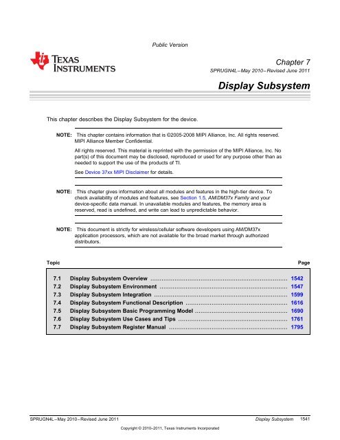
Figure 7-1 shows a block diagram of the display subsystem.<br />
1542 <strong>Display</strong> <strong>Subsystem</strong> SPRUGN4L–May 2010–Revised June 2011<br />
Copyright © 2010–2011, Texas Instruments Incorporated
Device<br />
PRCM<br />
L4 interconnect<br />
L3 interconnect<br />
System DMA<br />
controller<br />
(sDMA)<br />
MPU<br />
subsystem<br />
interrupt<br />
controller<br />
IVA2.2<br />
subsystem<br />
interrupt<br />
controller<br />
System<br />
control<br />
module<br />
L3 clock<br />
L4 clock<br />
Functional clock1<br />
Functional clock2<br />
54-MHz clock<br />
4<br />
DSS_L3_ICLK<br />
DSS_L4_ICLK<br />
DSS1_ALWON_FCLK<br />
DSS2_ALWON_FCLK<br />
DSS_TV_FCLK<br />
DSI1_PLL_FCLK<br />
DSI2_PLL_FCLK<br />
DSS_LINE_TRIGGER<br />
DSS_DMA_REQ[3:0]<br />
DSS_IRQ<br />
<strong>Display</strong><br />
controller<br />
Syncs<br />
DSI<br />
protocol<br />
engine<br />
<strong>Display</strong> subsystem<br />
Digital data<br />
24<br />
TV syncs<br />
Data<br />
Controls<br />
Public Version<br />
www.ti.com <strong>Display</strong> <strong>Subsystem</strong> Overview<br />
Figure 7-1. <strong>Display</strong> <strong>Subsystem</strong> Highlight<br />
Remote<br />
frame buffer<br />
interface<br />
TV out<br />
encoder<br />
Video DAC<br />
stage<br />
TVACEN<br />
TVOUTBYPASS<br />
COMP_EN<br />
DSI<br />
complex I/O<br />
DSI<br />
PLL<br />
controller<br />
DSS_PCLK<br />
DSS_VSYNC<br />
DSS_HSYNC<br />
DSS_ACBIAS<br />
DSS_DATA[17:6]<br />
DSS_DATA[23:18]<br />
TVINT<br />
Composite/Luma<br />
DSS_DATA[5:0]<br />
DSI_DX0<br />
DSI_DY0<br />
DSI_DX1<br />
DSI_DY1<br />
DSI_DX2<br />
DSI_DY2<br />
Status<br />
Chroma<br />
PLL control<br />
Pin multiplexing<br />
Pin multiplexing<br />
DSI PLL<br />
HS divider<br />
GPIO2<br />
dss_pclk<br />
dss_vsync<br />
dss_hsync<br />
dss_acbias<br />
dss_data[17:6]<br />
dss_data[23:18]<br />
cvideo1_out<br />
cvideo2_out<br />
cvideo1_vfb<br />
cvideo2_vfb<br />
cvideo1_rset<br />
vdda_dac<br />
vssa_dac<br />
dss_data[0]/dsi_dx0<br />
dss_data[1]/ dsi_dy0<br />
dss_data[2]/ dsi_dx1<br />
dss_data[3]/ dsi_dy1<br />
dss_data[4]/ dsi_dx2<br />
dss_data[5]/ dsi_dy2<br />
NOTE: For more information about connecting the LOCK, RECAL, and TVINT signals through the<br />
GPIO2 and GPIO3 modules, see <strong>Chapter</strong> 25, GPIO.<br />
The display subsystem includes the following main features:<br />
• <strong>Display</strong> controller<br />
– <strong>Display</strong> modes<br />
vdds_dsi<br />
vdd_dsi<br />
vss_dsi<br />
camdss-001<br />
• Programmable pixel display modes (1, 2, 4, 8, 12, 16, and 24 bits-per-pixel [BPP] modes)<br />
• Programmable display size supported:<br />
SPRUGN4L–May 2010–Revised June 2011 <strong>Display</strong> <strong>Subsystem</strong><br />
Copyright © 2010–2011, Texas Instruments Incorporated<br />
1543
Public Version<br />
<strong>Display</strong> <strong>Subsystem</strong> Overview www.ti.com<br />
• XGA - 1024 x 768 VESA timings at 60 fps (pixel clock = 63.5 MHz)<br />
• WXGA - 1280 x 800 VESA timings at 59.91 fps (pixel clock = 71 MHz)<br />
• SXGA+ - 1400 x 1050 direct drive of LCD with minimal blanking at 50 fps (pixel clock = 75<br />
MHz)<br />
• HD 720p - 1280 x 720 at 60 fps (pixel clock = 74.25 MHz)<br />
• 256 x 24-bit entries palette in red, green, and blue (RGB)<br />
• Programmable pixel rate up to 75 MHz<br />
NOTE: The panel size is programmable and can be any width that is a multiple of 8 pixels (line<br />
length) in the range [1:2048] pixels (in the case of the RFBI mode, the minimum transfer<br />
size is a byte). The maximum resolution is 2048 (lines) x 2048 (pixels).<br />
– <strong>Display</strong> support<br />
• Four types of displays are supported: Passive (super-twist nematic [STN]) and active (thin-film<br />
transistor [TFT]) colors, passive (STN), and active (TFT) monochromes.<br />
• 4-/8-bit monochrome passive matrix panel interface support (15 grayscale levels supported<br />
using dithering block)<br />
• 8-bit color passive matrix panel interface support (3375 colors supported for a color panel using<br />
dithering block)<br />
• 12-/16-/18-/24-bit active matrix panel interface support (replicated or dithered encoded pixel<br />
values)<br />
• Remote frame buffer support through the RFBI module<br />
• Partial display through the RFBI module<br />
• Second 24-bit digital output<br />
• Multiple-cycle output format on 8-/9-/12-/16-bit interface time division multiplexing (TDM)<br />
• HDMI through external bridge<br />
– Signal processing<br />
• Overlay support for graphics (ARGB, RGBA, RGB, or Color Look-Up Table (CLUT)) and video1<br />
(YCbCr 4:2:2, RGB), video2 (YCbCr 4:2:2, or ARGB, RGBA, RGB)<br />
• Programmable video resizer independent horizontal and vertical resampling: Upsampling (up to<br />
x8) and downsampling (down to 1/4), maximum input width of 1024 pixels in 5-tap mode, and<br />
2048 pixels in 3-tap configurations; no limitation on input height<br />
• Rotation 90-, 180-, and 270-degrees with DISPC DMA engine<br />
• Transparency color key (source and destination)<br />
• Synchronized buffer update<br />
• Programmable video color space conversion YCbCr 4:2:2 into RGB<br />
• Hardware cursor<br />
• Gamma curve support on LCD output<br />
• Multiple-buffer support<br />
• Mirroring support<br />
• Programmable color phase rotation (CPR)<br />
• Alpha blending support (no rescaling in ARGB or RGBA formats), with pre-multiplied alpha<br />
control<br />
– Advanced<br />
• Self-refresh using the DMA FIFO<br />
• Arbitration between high/low priority (graphics video1 and video2)<br />
• FIFO handcheck in STALL mode<br />
– Power modes: Low-power saving modes<br />
• RFBI (MIPI® DBI protocol)<br />
– Access to remote frame buffer (RFB) direct microprocessor unit (MPU) interface<br />
• Sends commands to the RFB panel through the L4 interconnect<br />
• Sends data, received from the display controller or from the MPU through the DISPC pixel data<br />
bus, to the RFB panel<br />
1544 <strong>Display</strong> <strong>Subsystem</strong> SPRUGN4L–May 2010–Revised June 2011<br />
Copyright © 2010–2011, Texas Instruments Incorporated
Public Version<br />
www.ti.com <strong>Display</strong> <strong>Subsystem</strong> Overview<br />
• Reads data/status from the RFB to the L4 interconnect<br />
– RFB interface<br />
• 8-/9-/12-/16-bit 8086-series parallel interface<br />
• Two programmable configurations for two devices connected to the RFBI module<br />
– Data formats<br />
• Programmable pixel modes (12-/16-/18-/24-BPP modes in RGB format)<br />
• Programmable output formats on one/multiple cycles per pixel (data from the display controller<br />
and from the L4 interconnect)<br />
– Interconnect/FIFO<br />
• One slave port with DMA request and interconnect FIFO of 24x32-bit depth (for write access to<br />
DSS.RFBI_DATA register only)<br />
• One video port FIFO of 8 × 24-bit depth receiving data from the display controller<br />
• MIPI DSI<br />
– Transfer pixels and data received on the video port or L4 interconnect to the display through the<br />
DSI DSI_PHY<br />
– The maximum resolution supported on the video port is XGA at 60 fps with 24-bit pixels (maximum<br />
pixel clock of 67 MHz) for low voltage.<br />
– Supports video mode and command mode<br />
– Bidirectional data link support (only one data lane is used in reverse direction in command mode)<br />
– Supports up to two data-configurable lanes, in addition to the clock signaling (minimum of one data<br />
link and maximum of two, depending on speed, signal integrity requirements, and number of<br />
displays)<br />
– Maximum data rate of up to 900 Mbps per data pair<br />
– Data splitter for 2-data lane configuration<br />
– Error-correction code (ECC) and check-sum generation<br />
– Burst support for the video mode<br />
– RGB16, RGB18 packed and nonpacked, and RGB24 formats supported for video mode<br />
– Serial configuration port (SCP) for the DSI_PHY complex I/O and DSI PLL<br />
– Connection to the DSI_PHY complex I/O through PPI<br />
– Data interleaving support for one synchronous stream (video mode) from the display controller and<br />
up to three interleaved asynchronous streams (command mode) from the interconnect concurrently<br />
– Data interleaving supports up to four interleaved asynchronous streams (command mode) from the<br />
interconnect or video port when there is no video mode<br />
– MIPI DCS support (transparent to the protocol engine, no decoding and interpretation of the<br />
information from and to the peripheral)<br />
– Supports selection between low-power state and HS mode between HS packet transfers<br />
– Generic data type (DT) support<br />
NOTE: The DSI pins are multiplexed with LCD parallel outputs.<br />
• Video encoder<br />
– NTSC/PAL encoder outputs with the following standards:<br />
• NTSC-J, M<br />
• PAL-B, D, G, H, I<br />
• PAL-M<br />
– CGMS-A as described in the CEA-608-x Standard.<br />
– Input data interface compatible with the following protocols:<br />
• 24-bit input bus compatible with external sync<br />
• RGB 4:4:4<br />
– Dual output data 10-bit interface for two internal digital-to-analog converters (DACs) that support:<br />
• Composite video (CVBS)<br />
• Separate video (S-video)<br />
SPRUGN4L–May 2010–Revised June 2011 <strong>Display</strong> <strong>Subsystem</strong><br />
Copyright © 2010–2011, Texas Instruments Incorporated<br />
1545
Public Version<br />
<strong>Display</strong> <strong>Subsystem</strong> Overview www.ti.com<br />
– TV output data supports ITU-R BT 470-7 recommendation standard for consumer market<br />
– Master clock input 13.5 MHz, 27 MHz (supports ITU-R 601 sampling for NTSC/PAL), and 54 MHz<br />
– Programmable horizontal sync, vertical timing, and waveforms<br />
– Programmable subcarrier frequency and SCH<br />
– Internal test pattern generation (color bar, flat field, color burst)<br />
– 2x/4x oversampling<br />
– Supports square pixel sampling (NTSC: 12.27 MHz, 24.54 MHz, 49.09 MHz PAL: 14.75 MHz,<br />
29.5 MHz, 59 MHz)<br />
CAUTION<br />
In square pixel mode, an external clock generator is required to provide<br />
sampling frequencies.<br />
– TV detection gating pulse generation<br />
1546 <strong>Display</strong> <strong>Subsystem</strong> SPRUGN4L–May 2010–Revised June 2011<br />
Copyright © 2010–2011, Texas Instruments Incorporated
Public Version<br />
www.ti.com <strong>Display</strong> <strong>Subsystem</strong> Environment<br />
7.2 <strong>Display</strong> <strong>Subsystem</strong> Environment<br />
This section describes the two main functions handled by the display subsystem:<br />
• LCD support<br />
• TV display support<br />
7.2.1 LCD Support<br />
LCD panels can be connected to the display subsystem of the device using parallel and/or serial<br />
interfaces.<br />
Table 7-1 provides more details on the supported interfaces to LCD panels, and the respective pad and<br />
signal configurations.<br />
SPRUGN4L–May 2010–Revised June 2011 <strong>Display</strong> <strong>Subsystem</strong><br />
Copyright © 2010–2011, Texas Instruments Incorporated<br />
1547
Public Version<br />
<strong>Display</strong> <strong>Subsystem</strong> Environment www.ti.com<br />
Table 7-1. LCD Interface Signals and Configurations<br />
Pads and Signals Configuration Possible Operational Interfaces<br />
Pad names at Pads Property Basic signal multiplexing on pads Additional signal multiplexing on Simultaneous Sequential<br />
device level pads<br />
boundary.<br />
Parallel Parallel Serial Interface, Parallel Parallel "1. Parallel "1. Parallel "1. Parallel<br />
Interface, Interface, RFBI DSI. Interface, Interface, RFBI Interface, Interface, Interface,<br />
Bypass Mode. mode. Bypass Mode. mode. Bypass mode RFBI-0 mode RFBI-0 mode<br />
24-bit 16-bit 16-bit<br />
2. Serial 2. Serial 2. Parallel<br />
Interface, DSI (2 Interface, DSI (2 Interface,<br />
data lanes)" data lanes)" RFBI-1 mode<br />
16-bit"<br />
dss_hsync <strong>Display</strong> DISPC_HSYNC RFBI_CS0 DISPC RFBI (CS0) RFBI (CS0)<br />
subsystem<br />
dss_vsync DISPC_VSYNC RFBI_WR RFBI RFBI<br />
dss_pclk DISPC_PCLK RFBI_RD<br />
dss_acbias DISPC_ACBIAS RFBI_A0<br />
dss_data0 DISPC_DATA_L RFBI_DA0 DSI_DX0 DSI DSI RFBI_DA [0-5]<br />
CD0<br />
dss_data1 DISPC_DATA_L RFBI_DA1 DSI_DY0<br />
CD1<br />
dss_data2 DISPC_DATA_L RFBI_DA2 DSI_DX1<br />
CD2<br />
dss_data3 DISPC_DATA_L RFBI_DA3 DSI_DY1<br />
CD3<br />
dss_data4 DISPC_DATA_L RFBI_DA4 DSI_DX2<br />
CD4<br />
dss_data5 DISPC_DATA_L RFBI_DA5 DSI_DY2<br />
CD5<br />
dss_data6 DISPC_DATA_L RFBI_DA6 DISPC_DATA_L RFBI_DA [6-15] RFBI_DA [6-15]<br />
CD6 CD [6-17]<br />
dss_data7 DISPC_DATA_L RFBI_DA7<br />
CD7<br />
dss_data8 DISPC_DATA_L RFBI_DA8<br />
CD8<br />
dss_data9 DISPC_DATA_L RFBI_DA9<br />
CD9<br />
dss_data10 DISPC_DATA_L RFBI_DA10<br />
CD10<br />
dss_data11 DISPC_DATA_L RFBI_DA11<br />
CD11<br />
dss_data12 DISPC_DATA_L RFBI_DA12<br />
CD12<br />
1548<strong>Display</strong> <strong>Subsystem</strong> SPRUGN4L–May 2010–Revised June 2011<br />
Copyright © 2010–2011, Texas Instruments Incorporated
Public Version<br />
www.ti.com <strong>Display</strong> <strong>Subsystem</strong> Environment<br />
Table 7-1. LCD Interface Signals and Configurations (continued)<br />
Pads and Signals Configuration Possible Operational Interfaces<br />
Pad names at Pads Property Basic signal multiplexing on pads Additional signal multiplexing on Simultaneous Sequential<br />
device level pads<br />
boundary.<br />
Parallel Parallel Serial Interface, Parallel Parallel "1. Parallel "1. Parallel "1. Parallel<br />
Interface, Interface, RFBI DSI. Interface, Interface, RFBI Interface, Interface, Interface,<br />
Bypass Mode. mode. Bypass Mode. mode. Bypass mode RFBI-0 mode RFBI-0 mode<br />
24-bit 16-bit 16-bit<br />
2. Serial 2. Serial 2. Parallel<br />
Interface, DSI (2 Interface, DSI (2 Interface,<br />
data lanes)" data lanes)" RFBI-1 mode<br />
16-bit"<br />
dss_data13 DISPC_DATA_L RFBI_DA13<br />
CD13<br />
dss_data14 DISPC_DATA_L RFBI_DA14 RFBI_DA [6-15] RFBI_DA [6-15]<br />
CD14<br />
dss_data15 <strong>Display</strong> DISPC_DATA_L RFBI_DA15 DISPC_DATA_L<br />
subsystem CD15 CD [6-17]<br />
dss_data16 DISPC_DATA_L RFBI_TE_VSYN "RFBI(sync0)" "RFBI(sync0)"<br />
CD16 C0<br />
dss_data17 DISPC_DATA_L RFBI_HSYNC0<br />
CD17<br />
dss_data18 DISPC_DATA_L RFBI_TE_VSYN DISPC_DATA_L RFBI_DA0 DISPC_DATA_L RFBI_DA [0-5] "RFBI(sync1)"<br />
CD18 C1 CD0 CD [0-5]<br />
dss_data19 DISPC_DATA_L RFBI_HSYNC1 DISPC_DATA_L RFBI_DA1<br />
CD19 CD1<br />
dss_data20 DISPC_DATA_L RFBI_CS1 DISPC_DATA_L RFBI_DA2 RFBI (CS1)<br />
CD20 CD2<br />
dss_data21 DISPC_DATA_L DISPC_DATA_L RFBI_DA3<br />
CD21 CD3<br />
dss_data22 DISPC_DATA_L DISPC_DATA_L RFBI_DA4<br />
CD22 CD4<br />
dss_data23 DISPC_DATA_L DISPC_DATA_L RFBI_DA5<br />
CD23 CD5<br />
SPRUGN4L–May 2010–Revised June 2011 <strong>Display</strong> <strong>Subsystem</strong>1549<br />
Copyright © 2010–2011, Texas Instruments Incorporated
Public Version<br />
<strong>Display</strong> <strong>Subsystem</strong> Environment www.ti.com<br />
Table 7-1. LCD Interface Signals and Configurations (continued)<br />
Pads and Signals Configuration Possible Operational Interfaces<br />
Pad names at Pads Property Basic signal multiplexing on pads Additional signal multiplexing on Simultaneous Sequential<br />
device level pads<br />
boundary.<br />
Parallel Parallel Serial Interface, Parallel Parallel "1. Parallel "1. Parallel "1. Parallel<br />
Interface, Interface, RFBI DSI. Interface, Interface, RFBI Interface, Interface, Interface,<br />
Bypass Mode. mode. Bypass Mode. mode. Bypass mode RFBI-0 mode RFBI-0 mode<br />
24-bit 16-bit 16-bit<br />
2. Serial 2. Serial 2. Parallel<br />
Interface, DSI (2 Interface, DSI (2 Interface,<br />
data lanes)" data lanes)" RFBI-1 mode<br />
16-bit"<br />
sys_boot0 System control DISPC_DATA_L DISPC_DATA_L<br />
module CD18 CD [18-23]<br />
sys_boot1 DISPC_DATA_L<br />
CD19<br />
sys_boot3 DISPC_DATA_L<br />
CD20<br />
sys_boot4 DISPC_DATA_L<br />
CD21<br />
sys_boot5 DISPC_DATA_L<br />
CD22<br />
sys_boot6 DISPC_DATA_L<br />
CD23<br />
The DISPC_DATA_LCD[23:18] data is additionally multiplexed on the sys_boot device pads to allow simultaneous availability of the DSI interface<br />
and the complete parallel 24-bit DSS interface.<br />
NOTE: The DISPC_DATA_LCD[5:0] data multiplexed with the DSI signals on dss_data[5:0] pads is limited to up to 60 MHz pixel clock<br />
frequency. If the parallel 18/24-bit interface in bypass mode with a pixel clock above 60 MHz is required, the DISPC_DATA_LCD[5:0]<br />
multiplexed on dss_data[23:18] pads, and DISPC_DATA_LCD[23:18] multiplexed on sys_boot pads must be used.<br />
NOTE: Table 7-1 shows only the DSS capabilities of supporting simultaneous and sequential LCD interfaces due to the additional signal<br />
multiplexing, without describing explicitly all possible configurations.<br />
For more information on signals multiplexing, see <strong>Chapter</strong> 13, System Control Module. The parallel interface connectivity is detailed in<br />
Section 7.2.1.1, Parallel Interface. For more details on the serial interface, see Section 7.2.1.2, DSI Serial Interface.<br />
1550<strong>Display</strong> <strong>Subsystem</strong> SPRUGN4L–May 2010–Revised June 2011<br />
Copyright © 2010–2011, Texas Instruments Incorporated
Public Version<br />
www.ti.com <strong>Display</strong> <strong>Subsystem</strong> Environment<br />
7.2.1.1 Parallel Interface<br />
In parallel interface, the paths of the display subsystem modules are the display controller and the RFBI.<br />
The display controller provides the required control signals to interface the memory frame buffer (SDRAM<br />
or SRAM) directly to the external displays. The display controller is connected to the memory through the<br />
L3 interconnect and has its own DMA (with embedded FIFOs) to read data from the system memory. The<br />
L3 interconnect is the master port, while the L4 interconnect is the slave port of the display subsystem.<br />
The display controller has two I/O pad modes at the module level:<br />
• RFBI mode (RFBI enabled), which implements the MIPI DBI 2.0 protocol<br />
• Bypass mode (RFBI disabled), which implements the MIPI DPI 1.0 protocol<br />
The DSS.DISPC_CONTROL[16:15] GPOUT[1:0] bits control selection of the display subsystem modules<br />
(see Table 7-2).<br />
Table 7-2. I/O Pad Mode Selection<br />
DSS.DISPC_CONTROL[16] GPOUT1 DSS.DISPC_CONTROL[15] GPOUT0 Mode<br />
0 0 Reset<br />
0 1 RFBI mode<br />
1 0 Invalid<br />
1 1 Bypass mode<br />
The RFB of the LCD panel is connected directly to the RFBI module of the device. The RFBI controls the<br />
reads/writes from/to the RFB. The RFBI receives the output from the DISPC (which takes data from the<br />
memory) and generates the signals to control the LCD panel. Through the RFBI, the MPU can send<br />
commands or parameter/display data to the LCD panel and directly set the DISPC registers to read/write<br />
the data from/to the memory in the LCD panel. The RFBI can manage up to two LCD panels when the<br />
serial interface is not used.<br />
7.2.1.1.1 Parallel Interface in RFBI Mode (MIPI DBI Protocol)<br />
Figure 7-2 shows the LCD support parallel interface in RFBI mode (example for 16-bit data interface).<br />
SPRUGN4L–May 2010–Revised June 2011 <strong>Display</strong> <strong>Subsystem</strong><br />
Copyright © 2010–2011, Texas Instruments Incorporated<br />
1551
<strong>Display</strong> subsystem<br />
<strong>Display</strong><br />
controller<br />
RFBI<br />
RFBI_DA[15:0]<br />
RFBI_RD<br />
RFBI_WR<br />
RFBI_A0<br />
RFBI_CS0<br />
RFBI_TE_VSYNC0<br />
RFBI_HSYNC0<br />
RFBI_TE_VSYNC1<br />
RFBI_HSYNC1<br />
Public Version<br />
<strong>Display</strong> <strong>Subsystem</strong> Environment www.ti.com<br />
Figure 7-2. LCD Support Parallel Interface (RFBI Mode)<br />
RFBI_CS1<br />
dss_data[15:0]<br />
dss_pclk<br />
dss_vsync<br />
dss_acbias<br />
dss_hsync<br />
dss_data16<br />
dss_data17<br />
dss_data18<br />
dss_data19<br />
dss_data20<br />
LCD<br />
panel 1<br />
with RFB<br />
LCD<br />
panel 2<br />
with RFB<br />
NOTE: Configure the DSS.RFBI_CONTROL[3:2] CONFIGSELECT bit field to drive signals for LCD<br />
1 only, LCD 2 only, or both LCD 1 and LCD 2.<br />
Table 7-3 describes the interface signals to/from the LCD panel in RFBI mode.<br />
Signal Name Type (1) Description<br />
RFBI_DA[15:0] I/O RFBI I/O data<br />
Table 7-3. LCD Interface Signals (RFBI Mode)<br />
RFBI_RD O Read access signal<br />
RFBI_WR O Write access signal<br />
RFBI_A0 O Command/data selection signal<br />
RFBI_CS0 O Chip-select (CS) signal for LCD 1<br />
RFBI_CS1 O CS signal for LCD 2<br />
RFBI_TE_VSYNC0 I Tearing effect (TE) synchronization signal (TE or VSYNC for LCD panel 1)<br />
RFBI_HSYNC0 I HSYNC from LCD panel 1<br />
RFBI_TE_VSYNC1 I TE synchronization signal (TE or VSYNC for LCD panel 2)<br />
RFBI_HSYNC1 I HSYNC from LCD panel 2<br />
(1) I = Input, O = Output<br />
• RFBI_DA[15:0]: The pixel data comprises the RFBI pixel data (bits 15:0). A write/read command must<br />
be sent to the LCD panel to send/read the data.<br />
Before any data access, the application must send commands and parameters when it is necessary to<br />
configure an LCD panel. The data is used as input in read operations during production test and also<br />
to read the status of the registers in the LCD panel and pixels from the embedded frame buffer in the<br />
LCD panel module. RFBI_DA is multiplexed at the chip-level boundary with dss_data [15:0].<br />
• RFBI_RD: This is the read-enable signal used to indicate when a read from the embedded memory in<br />
the LCD panel is ongoing. The RFBI registers describe the behavior of the read signal (off/on/cycle<br />
time). The polarity of the read-enable signal is programmable. This signal is multiplexed at the<br />
1552 <strong>Display</strong> <strong>Subsystem</strong> SPRUGN4L–May 2010–Revised June 2011<br />
Copyright © 2010–2011, Texas Instruments Incorporated<br />
dss-002
DSS_L4_ICLK<br />
TE<br />
VSYNC<br />
HSYNC<br />
Public Version<br />
www.ti.com <strong>Display</strong> <strong>Subsystem</strong> Environment<br />
chip-level boundary with dss_pclk. The read is used to get status/data information from the LCD panel.<br />
• RFBI_WR: The write-enable signal is used to indicate when a write is ongoing. The RFBI registers<br />
describe the behavior of the write signal (off/on/cycle time). The polarity of the write-enable signal is<br />
programmable. This signal is multiplexed at the chip-level boundary with dss_vsync.<br />
• RFBI_A0: The signal is asserted to indicate its status: Command or data. The polarity is programmable<br />
and the status of the signal depends on the RFBI registers written by the application<br />
(CMD/READ/STATUS/PARAM/PIXEL). The register in use by the hardware defines the status of<br />
RFBI_A0. The order of the writes/reads to the RFBI registers CMD/READ/STATUS/PARAM/PIXEL<br />
defines the transitions of A0. This signal is multiplexed at the chip-level boundary with dss_acbias.<br />
• RFBI_CSx: The signal is the chip-select (CSx) asserted to indicate which LCD panel is selected and<br />
must be ready to receive/transmit commands and data. When RE or WE is on, CSx must not be<br />
changed (x = 0 for LCD panel 1; x = 1 for LCD panel 2). CS0 is multiplexed at the chip-level boundary<br />
with dss_hsync, and CS1 is multiplexed at the chip-level boundary with dss_data[20].<br />
• RFBI_TE_VSYNCx: Based on the trigger mode selected, the signal is the TE pulse signal or the LCD<br />
panel VSYNC (vertical synchronization) pulse signal. RFBI_TE_VSYNCx is used by the TE logic as the<br />
synchronization signal to send the pixel to the LCD panel.<br />
To select the trigger mode, configure the DSS.RFBI_CONFIGi[3:2] TRIGGERMODE bit field (0x0:<br />
Internal trigger mode with the DSS.RFBI_CONTROL[4] ITE bit, 0x1: External trigger mode with the TE<br />
signal RFBI_TE_VSYNCx, 0x2: External trigger mode with the RFBI_TE_VSYNCx, and<br />
RFBI_HSYNCx signals with the programmable line counter).<br />
These signals are multiplexed at the chip-level boundary with dss_data[16] (RFBI_TE_VSYNC0) and<br />
dss_data[18] (RFBI_TE_VSYNC1) (LCD panel 1: x = 0; LCD panel 2: x = 1).<br />
• RFBI_HSYNCx: The HSYNC pulse signals indicate to the RFBI module when horizontal<br />
synchronization occurs. The polarity of the HSYNC signals is programmable. The minimum pulse width<br />
of the signal is two L4 cycles. RFBI_HSYNC is used by the TE logic as a synchronization signal to<br />
send the pixel to the LCD panel. These signals are multiplexed at the chip-level boundary with<br />
dss_data[17] (RFBI_HSYNC0) and dss_data[19] (RFBI_HSYNC1) (LCD panel 1: x = 0; LCD panel 2: x<br />
= 1).<br />
7.2.1.1.1.1 Description of the TE Pulse Signal<br />
The externally-generated TE synchronization signal is a logical OR or AND operation between the HSYNC<br />
and VSYNC signals (see Figure 7-3). The logical operation (OR or AND) depends on the HSYNC and<br />
VSYNC signals polarity. The VSYNC signal indicates to the RFBI module when vertical synchronization<br />
occurs; the HSYNC signal indicates to the RFBI module when horizontal synchronization occurs.<br />
Figure 7-3. External Generation of TE Signal Based on Logical OR Operation Between HSYNC and<br />
VSYNC (Active-High)<br />
The RFBI module detects the VSYNC and HSYNC pulses embedded in the received signal. VSYNC is<br />
detected based on the minimum pulse width defined by the DSS.RFBI_VSYNC_WIDTH register.<br />
HSYNC is detected based on the minimum pulse width defined by the DSS.RFBI_HSYNC_WIDTH<br />
register.<br />
The signal is generated from external logic based on the VSYNC/HSYNC of the LCD panel. The<br />
automatic trigger can be programmed based on the RFBI_TE signal or use a bit field in the RFBI registers<br />
to start data capture.<br />
SPRUGN4L–May 2010–Revised June 2011 <strong>Display</strong> <strong>Subsystem</strong><br />
Copyright © 2010–2011, Texas Instruments Incorporated<br />
dss-003<br />
1553
<strong>Display</strong> subsystem<br />
<strong>Display</strong><br />
controller<br />
DISPC_DATA_LCD[23:0]<br />
DISPC_PCLK<br />
DISPC_VSYNC<br />
DISPC_HSYNC<br />
DISPC_ACBIAS<br />
Public Version<br />
<strong>Display</strong> <strong>Subsystem</strong> Environment www.ti.com<br />
The polarity of the TE signal is programmable. The HSYNC and VSYNC pulses embedded in the TE<br />
signal have the same polarity, which is active high for an ORed signal and active low for an ANDed signal.<br />
The minimum pulse width of the signal is two L4 cycles. Hardware resets the line counter when the<br />
VSYNC occurs and increments it at every HSYNC. Transfer to the LCD panel begins when the line<br />
counter reaches the programmable line number.<br />
7.2.1.1.2 Parallel Interface in Bypass Mode (MIPI DPI Protocol)<br />
When bypass mode is enabled, the display controller must be set to use it.<br />
Figure 7-4 shows the LCD support parallel interface in bypass mode.<br />
Figure 7-4. LCD Support Parallel Interface (Bypass Mode)<br />
RFBI<br />
dss_data[23:0]<br />
dss_pclk<br />
dss_vsync<br />
dss_hsync<br />
dss_acbias<br />
Table 7-4 describes the interface signals to/from the LCD panel in bypass mode.<br />
Table 7-4. LCD Interface Signals (Bypass Mode)<br />
Signal Name Type (1) Description<br />
DISPC_DATA_LCD[23:0] O LCD data from the display controller module<br />
DISPC_PCLK O Pixel CLK from the display controller module<br />
DISPC_VSYNC O VSYNC from the display controller module<br />
DISPC_HSYNC O HSYNC from the display controller module<br />
DISPC_ACBIAS O ACBIAS from the display controller module<br />
(1) I = Input, O = Output, I/O = Input/Output<br />
LCD<br />
panel<br />
• DISPC_DATA_LCD[23:0]: The panel pixel data comes directly from the display controller module.<br />
DISPC_DATA_LCD is connected at the chip-level boundary with dss_data[23:0].<br />
• DISPC_PCLK: This signal is the pixel clock that comes directly from the display controller. This signal<br />
is multiplexed at the chip-level boundary with dss_pclk.<br />
• DISPC_VSYNC: Uses the vertical synchronization signal from the display controller. The LCD frame<br />
clock (VSYNC) toggles after all the lines in a frame are transmitted to the LCD panel and a<br />
programmable number of line clock cycles has elapsed both at the beginning and at the end of each<br />
frame. This signal is multiplexed with dss_vsync at the chip-level boundary.<br />
• DISPC_HSYNC: Uses the horizontal synchronization signal from the display controller. The LCD line<br />
clock (HSYNC) toggles after all pixels in a line are transmitted to the LCD panel and a programmable<br />
number of pixel clock wait-states elapse, both at the beginning and at the end of each line. This signal<br />
is multiplexed on the chip-level boundary with dss_hsync.<br />
• DISPC_ACBIAS: Uses the ac-bias signal from the display controller.<br />
– In passive matrix technology, the ac-bias signal is configured to transition each time a<br />
programmable number of line clocks occurs. To prevent a dc charge within the screen pixels, the<br />
power and ground supplies of the panel are periodically switched. The DISPC signals the panel to<br />
switch the polarity by toggling the ac-bias pin.<br />
1554 <strong>Display</strong> <strong>Subsystem</strong> SPRUGN4L–May 2010–Revised June 2011<br />
Copyright © 2010–2011, Texas Instruments Incorporated<br />
dss-004
LCD<br />
controller<br />
output<br />
pins<br />
Pixel clock<br />
Public Version<br />
www.ti.com <strong>Display</strong> <strong>Subsystem</strong> Environment<br />
– In active matrix technology, the ac-bias signal acts as an output-enable signal to indicate when data<br />
must be latched using the pixel clock. This signal is multiplexed on the chip-level boundary with<br />
dss_acbias.<br />
7.2.1.1.3 LCD Output and Data Format for the Parallel Interface<br />
This section describes the pixel data bus and shows timing diagrams of transactions and synchronizations<br />
in both RFBI and bypass modes.<br />
Figure 7-5 through Figure 7-11 show the pixel data bus for bypass mode, depending on the use of 4-, 8-,<br />
12-, 16-, 18-, or 24-pixel data output pins. In RFBI mode, the pixel data bus is reformatted in accordance<br />
with the input and output data bus width.<br />
Table 7-5 lists the number of displayed pixels per pixel clock cycle based on the type of display panel.<br />
Table 7-5. Number of <strong>Display</strong>ed Pixels per Pixel Clock Cycle Based on <strong>Display</strong><br />
Type<br />
<strong>Display</strong> Panel Number of <strong>Display</strong>ed<br />
Pixels per Pixel Clock Cycle<br />
Monochrome 4-bit 4<br />
Monochrome 8-bit 8<br />
Passive matrix color 8/3<br />
Active matrix 1<br />
• Passive matrix technology, Monochrome mode<br />
Monochrome displays use either a 4-bit or 8-bit interface. Each bit represents one pixel (on or off),<br />
which means that either 4 or 8 pixels are sent to the LCD at each pixel clock.<br />
Figure 7-5 and Figure 7-6 show 4- and 8-bit monochrome displays, respectively.<br />
Figure 7-5. LCD Pixel Data Monochrome4 Passive Matrix<br />
Pix1<br />
Pix2<br />
Pix3<br />
Pix4<br />
Pixel data<br />
dss_data[0]<br />
dss_data[1]<br />
dss_data[2]<br />
dss_data[3]<br />
Pixel data [3:0]<br />
SPRUGN4L–May 2010–Revised June 2011 <strong>Display</strong> <strong>Subsystem</strong><br />
Copyright © 2010–2011, Texas Instruments Incorporated<br />
dss-005<br />
1555
<strong>Display</strong><br />
controller<br />
output pins<br />
Pixel clock<br />
LCD<br />
controller<br />
output pins<br />
Pixel clock<br />
(Pix3) G<br />
(Pix3) R<br />
(Pix2) B<br />
(Pix2) G<br />
(Pix2) R<br />
(Pix1) B<br />
(Pix1) G<br />
(Pix1) R<br />
Public Version<br />
<strong>Display</strong> <strong>Subsystem</strong> Environment www.ti.com<br />
Figure 7-6. LCD Pixel Data Monochrome8 Passive Matrix<br />
Pix1<br />
Pix2<br />
Pix3<br />
Pix4<br />
Pix5<br />
Pix6<br />
Pix7<br />
Pix8<br />
(Pix6) R<br />
(Pix5) B<br />
(Pix5) G<br />
(Pix5) R<br />
(Pix4) B<br />
(Pix4) G<br />
(Pix4) R<br />
(Pix3) B<br />
(Pix8) B<br />
(Pix8) G<br />
(Pix8) R<br />
(Pix7) B<br />
(Pix7) G<br />
(Pix7) R<br />
(Pix6) B<br />
(Pix6) G<br />
Pixel data<br />
dss_data[0]<br />
dss_data[1]<br />
dss_data[2]<br />
dss_data[3]<br />
dss_data[4]<br />
dss_data[5]<br />
dss_data[6]<br />
dss_data[7]<br />
Pixel data [7:0]<br />
• Passive matrix technology, color mode<br />
Color passive displays use 8-bit data input lines. In a given pixel clock cycle, each line represents one<br />
color component (red, green, or blue).<br />
Figure 7-7 shows an 8-bit color passive matrix display.<br />
Figure 7-7. LCD Pixel Data Color Passive Matrix<br />
dss-006<br />
Pixel data<br />
dss_data[0]<br />
dss_data[1]<br />
dss_data[2]<br />
dss_data[3]<br />
dss_data[4]<br />
dss_data[5]<br />
dss_data[6]<br />
dss_data[7]<br />
• Active matrix technology<br />
Active matrix displays bypass the STN dithering logic block and the output FIFO. Each line represents<br />
one pixel.<br />
Figure 7-8 through Figure 7-11 show 12-, 16-, 18-, and 24-active matrix displays, respectively.<br />
1556 <strong>Display</strong> <strong>Subsystem</strong> SPRUGN4L–May 2010–Revised June 2011<br />
Copyright © 2010–2011, Texas Instruments Incorporated<br />
Pixel<br />
data<br />
[7:0]<br />
dss-0<strong>07</strong>
LCD<br />
controller<br />
output pins<br />
Pixel clock<br />
(Pix1) B0<br />
(Pix1) B1<br />
(Pix1) B2<br />
(Pix1) B3<br />
(Pix1) G0<br />
(Pix1) G1<br />
(Pix1) G2<br />
(Pix1) G3<br />
(Pix1) R0<br />
(Pix1) R1<br />
(Pix1) R2<br />
(Pix1) R3<br />
(Pix2) B0<br />
(Pix2) B1<br />
(Pix2) B2<br />
(Pix2) B3<br />
(Pix2) G0<br />
(Pix2) G1<br />
(Pix2) G2<br />
(Pix2) G3<br />
(Pix2) R0<br />
(Pix2) R1<br />
(Pix2) R2<br />
(Pix2) R3<br />
Public Version<br />
www.ti.com <strong>Display</strong> <strong>Subsystem</strong> Environment<br />
Figure 7-8. LCD Pixel Data Color12 Active Matrix<br />
(Pix3) B0<br />
(Pix3) B1<br />
(Pix3) B2<br />
(Pix3) B3<br />
(Pix3) G0<br />
(Pix3) G1<br />
(Pix3) G2<br />
(Pix3) G3<br />
(Pix3) R0<br />
(Pix3) R1<br />
(Pix3) R2<br />
(Pix3) R3<br />
Pixel data<br />
dss_data[0]<br />
dss_data[1]<br />
dss_data[2]<br />
dss_data[3]<br />
dss_data[4]<br />
dss_data[5]<br />
dss_data[6]<br />
dss_data[7]<br />
dss_data[8]<br />
dss_data[9]<br />
dss_data[10]<br />
dss_data[11]<br />
SPRUGN4L–May 2010–Revised June 2011 <strong>Display</strong> <strong>Subsystem</strong><br />
Copyright © 2010–2011, Texas Instruments Incorporated<br />
Pixel<br />
data<br />
[11:0]<br />
dss-008<br />
1557
LCD<br />
controller<br />
output pins<br />
Pixel clock<br />
LCD<br />
controller<br />
output pins<br />
Pixel clock<br />
(Pix1) B0<br />
(Pix1) B1<br />
(Pix1) B2<br />
(Pix1) B3<br />
(Pix1) B4<br />
(Pix1) R0<br />
(Pix1) R1<br />
(Pix1) R2<br />
(Pix1) R3<br />
(Pix1) R4<br />
(Pix1) B0<br />
(Pix1) B1<br />
(Pix1) B5<br />
(Pix1) R0<br />
(Pix1) R3<br />
(Pix1) R4<br />
(Pix1) R5<br />
(Pix2) B0<br />
(Pix2) B1<br />
(Pix2) B2<br />
(Pix2) B3<br />
(Pix2) B4<br />
(Pix2) R0<br />
(Pix2) R1<br />
(Pix2) R2<br />
(Pix2) R3<br />
(Pix2) R4<br />
(Pix2) B0<br />
(Pix2) B1<br />
(Pix2) B5<br />
(Pix2) R0<br />
(Pix2) R3<br />
(Pix2) R4<br />
(Pix2) R5<br />
Public Version<br />
<strong>Display</strong> <strong>Subsystem</strong> Environment www.ti.com<br />
Figure 7-9. LCD Pixel Data Color16 Active Matrix<br />
(Pix3) B0<br />
(Pix3) B1<br />
(Pix3) B2<br />
(Pix3) B3<br />
(Pix3) B4<br />
(Pix3) R0<br />
(Pix3) R1<br />
(Pix3) R2<br />
(Pix3) R3<br />
(Pix3) R4<br />
Figure 7-10. LCD Pixel Data Color18 Active Matrix<br />
(Pix3) B0<br />
(Pix3) B1<br />
(Pix3) B5<br />
(Pix3) R0<br />
(Pix3) R3<br />
(Pix3) R4<br />
(Pix3) R5<br />
Pixel data<br />
dss_data[0]<br />
dss_data[1]<br />
dss_data[2]<br />
dss_data[3]<br />
dss_data[4]<br />
dss_data[11]<br />
dss_data[12]<br />
dss_data[13]<br />
dss_data[14]<br />
dss_data[15]<br />
Pixel data<br />
dss_data[0]<br />
dss_data[1]<br />
dss_data[5]<br />
dss_data[12]<br />
dss_data[15]<br />
dss_data[16]<br />
dss_data[17]<br />
Pixel<br />
data<br />
[15:0]<br />
dss-009<br />
Pixel<br />
data<br />
[17:0]<br />
1558 <strong>Display</strong> <strong>Subsystem</strong> SPRUGN4L–May 2010–Revised June 2011<br />
Copyright © 2010–2011, Texas Instruments Incorporated<br />
dss-010
LCD<br />
controller<br />
output pins<br />
DISPC_FCLK<br />
DISPC_PCLK<br />
DISPC_DATA_STALL<br />
DISPC_LCD_DATA[23:0]<br />
Pixel clock<br />
(Pix1) B0<br />
(Pix1) B1<br />
(Pix1) B7<br />
(Pix1) G0<br />
(Pix1) G7<br />
(Pix1) R0<br />
(Pix1) R5<br />
(Pix1) R6<br />
(Pix1) R7<br />
(Pix2) B0<br />
(Pix2) B1<br />
(Pix2) B7<br />
(Pix2) G0<br />
(Pix2) G7<br />
(Pix2) R0<br />
(Pix2) R5<br />
(Pix2) R6<br />
(Pix2) R7<br />
4_DISPC_CLK_cycle_for_assertion<br />
Public Version<br />
www.ti.com <strong>Display</strong> <strong>Subsystem</strong> Environment<br />
7.2.1.1.4 Transaction Timing Diagrams<br />
• Timing diagrams in flow control mode<br />
Figure 7-11. LCD Pixel Data Color24 Active Matrix<br />
(Pix3) B0<br />
(Pix3) B1<br />
(Pix3) B7<br />
(Pix3) G0<br />
(Pix3) G7<br />
(Pix3) R0<br />
(Pix3) R5<br />
(Pix3) R6<br />
(Pix3) R7<br />
Pixel data<br />
dss_data[0]<br />
dss_data[1]<br />
dss_data[7]<br />
dss_data[8]<br />
dss_data[15]<br />
dss_data[16]<br />
dss_data[21]<br />
dss_data[22]<br />
dss_data[23]<br />
PIXELS 1 PIXELS 2 PIXELS 3 PIXELS 4 PIXELS 5<br />
Pixel<br />
data<br />
[23:0]<br />
– Stall signal<br />
The stall signal is used in RFBI and DSI modes. In the case of RFBI mode, it is used to indicate<br />
when the display controller must stop sending data over the LCD output interface. The RFBI<br />
module asserts the stall signal to stop data output by the display controller. It is deasserted to<br />
indicate when new data must be outputted by the display controller.<br />
Figure 7-12. RFBI Data Stall Signal Diagram<br />
dss-011<br />
1_DISPC_CLK.cycle_after_for_de_assertion<br />
To avoid underflow of the DMA FIFO, the FIFO handcheck feature can be enabled by setting the<br />
DSS.DISPC_CONFIG[16] FIFOHANDCHECK bit to 1. The fullness of the FIFOs associated with<br />
the pipelines used for the LCD output is checked when the STALL signal is inactive before<br />
providing data to the pipeline. This prevents emptying the FIFO when the RFBI module requests<br />
data and there is not enough data in the display controller DMA FIFO. This feature must be enabled<br />
only when the STALL mode is used (DSS.DISPC_CONTROL[11] STALLMODE bit set to 1).<br />
When the FIFO handcheck feature is activated, the pixel transfer to the RFBI module during STALL<br />
inactivity period can be stopped (no DISPC_PCLK pulse) and restarted when there is enough data<br />
in the FIFO. The FIFO handcheck ensures that underflow cannot occur for the pipelines associated<br />
with the LCD output in RFBI mode. Figure 7-13 details the RFBI data stall with FIFO handcheck<br />
mode activated.<br />
SPRUGN4L–May 2010–Revised June 2011 <strong>Display</strong> <strong>Subsystem</strong><br />
Copyright © 2010–2011, Texas Instruments Incorporated<br />
dss-134<br />
1559
DISPC_FCLK<br />
DISPC_PCLK<br />
DISPC_DATA_STALL<br />
DISPC_LCD_DATA[23:0]<br />
L4_CLK<br />
RFBI_A0(D/C)<br />
RFBI_CSi<br />
(with i = 0, 1)<br />
RFBI_WR<br />
DISPC_CLK_cycles_for_assertion<br />
1_DISPC_CLK_cycle_for_de_assertion<br />
PIXELS 1 PIXELS 2 PIXELS 3<br />
WECycleTime<br />
CSOnTime<br />
CSOffTime<br />
WEOffTime<br />
WEOnTime<br />
Public Version<br />
<strong>Display</strong> <strong>Subsystem</strong> Environment www.ti.com<br />
Figure 7-13. RFBI Data Stall Signal Diagram With Handcheck<br />
– RFBI timing diagrams<br />
Table 7-6 lists the programmable timing fields. Figure 7-14 through Figure 7-16 show timing diagrams<br />
of read/write transactions to the LCD panel for the RFBI mode.<br />
Table 7-6. Programmable Timing Fields in RFBI Mode<br />
Timing Name Register Field Description<br />
CSOnTime DSS.RFBI_ONOFF_TIMEi[3:0] CS assertion time from start access time<br />
CSONTIME (with I = 0 or 1)<br />
CSOffTime DSS.RFBI_ONOFF_TIMEi[9:4] CS deassertion time from start access time<br />
CSOFFTIME (with I = 0 or 1)<br />
WeCycleTime DSS.RFBI_CYCLE_TIMEi[5:0] The time when A0 becomes valid until write cycle<br />
WECYCLETIME (with I = 0 or 1) completion<br />
WEOnTime DSS_RFBI_ONOFF_TIMEi[13:10] WE assertion delay time from start access time<br />
WEONTIME (with I = 0 or 1)<br />
WEOffTime DSS_RFBI_ONOFF_TIMEi[19:14] WE deassertion delay time from start access time<br />
WEOFFTIME (with I = 0 or 1)<br />
RECycleTime DSS.RFBI_CYCLE_TIMEi[11:6] The time when A0 becomes valid until read cycle<br />
RECYCLETIME (with I = 0 or 1) completion<br />
REOnTime DSS_RFBI_ONOFF_TIMEi[23:20] RE assertion delay time from start access time<br />
REONTIME (with I = 0 or 1)<br />
REOffTime DSS.RFBI_ONOFF_TIMEi[29:24] RE assertion delay time from start access time<br />
REOFFTIME (with I = 0 or 1)<br />
CSPulseWidth DSS.RFBI_CYCLE_TIMEi[17:12] The time when write cycle time or read cycle time<br />
CSPULSEWIDTH (with I = 0 or 1) completes<br />
Figure 7-14. Command Data Write<br />
WECycleTime<br />
CSOnTime<br />
RFBI_DA[15:0] DATA0 DATA1<br />
1560 <strong>Display</strong> <strong>Subsystem</strong> SPRUGN4L–May 2010–Revised June 2011<br />
Copyright © 2010–2011, Texas Instruments Incorporated<br />
dss-135<br />
dss-012
L4_CLK<br />
RFBI_A0(D/C)<br />
RFBI_CSi<br />
(with i = 0, 1)<br />
RFBI_RD<br />
RFBI_DA[15:0]<br />
L4_CLK<br />
RFBI_A0(D/C)<br />
RFBI_CSi<br />
(with i = 0, 1)<br />
RFBI_RD<br />
RFBI_WR<br />
RFBI_DA[15:0]<br />
RECycleTime<br />
CSOffTime<br />
CSOnTime<br />
REOnTime<br />
AccessTime<br />
CSOnTime<br />
REOffTime REOffTime<br />
CSOffTime<br />
CSOnTime<br />
Public Version<br />
www.ti.com <strong>Display</strong> <strong>Subsystem</strong> Environment<br />
Figure 7-15. <strong>Display</strong> Data Read<br />
DATA0 DATA1<br />
Figure 7-16. Read to Write and Write to Read<br />
RECycleTime WECycleTime<br />
CSPulseWidth CSPulseWidth<br />
CSOffTime CSOffTime<br />
CSOnTime<br />
CSOnTime<br />
READ0 WRITE0 READ1<br />
• Timing diagrams in bypass mode<br />
Figure 7-17 through Figure 7-32 show timing diagrams of synchronization signals and pixel clock in<br />
bypass mode for both passive matrix and active matrix panels. The display controller directly drives<br />
these signals, which are related to the programmable fields described in Table 7-7.<br />
Table 7-7. Programmable Fields in Bypass Mode<br />
Name Register Description<br />
PPL DSS.DISPC_SIZE_LCD[10:0] PPL bit field value + 1 Pixels per line (PPL)<br />
LPP DSS.DISPC_SIZE_LCD[26:16] LPP bit field value + 1 Lines per panel<br />
HBP DSS.DISPC_TIMING_H[31:20] HBP bit field value + 1 Horizontal back porch<br />
HFP DSS.DISPC_TIMING_H[19:8] HFP bit field value + 1 Horizontal front porch<br />
HSW DSS.DISPC_TIMING_H[7:0] HSW bit field value + 1 Horizontal synchronization pulse width<br />
VBP DSS.DISPC_TIMING_V[31:20] VBP bit field value Vertical back porch<br />
SPRUGN4L–May 2010–Revised June 2011 <strong>Display</strong> <strong>Subsystem</strong>1561<br />
Copyright © 2010–2011, Texas Instruments Incorporated<br />
dss-013<br />
dss-014
DISPC_PCLK<br />
DISPC_VSYNC<br />
DISPC_HSYNC<br />
DISPC_ACBIAS<br />
HSW VSW VBP HBP<br />
DISPC_DATA_LCD[23:0] PIXELS<br />
DISPC_PCLK<br />
DISPC_VSYNC<br />
DISPC_HSYNC<br />
DISPC_ACBIAS<br />
DISPC_DATA_LCD[23:0]<br />
Public Version<br />
<strong>Display</strong> <strong>Subsystem</strong> Environment www.ti.com<br />
Table 7-7. Programmable Fields in Bypass Mode (continued)<br />
Name Register Description<br />
VFP DSS.DISPC_TIMING_V[19:8] VFP bit field value Vertical front porch<br />
VSW DSS.DISPC_TIMING_V[7:0] VSW bit field value + 1 Vertical synchronization pulse width<br />
ONOFF DSS.DISPC_POL_FREQ[17] ONOFF bit DISPC_HSYNC and DISPC_VSYNC pixel clock<br />
control<br />
RF DSS.DISPC_POL_FREQ[16] RF bit DISPC_HSYNC and DISPC_VSYNC pixel clock<br />
edge control<br />
IEO DSS.DISPC_POL_FREQ[15] IEO bit Invert DISPC_ACBIAS<br />
IPC DSS.DISPC_POL_FREQ[14] IPC bit Invert DISPC_PCLK<br />
IHS DSS.DISPC_POL_FREQ[13] IHS bit Invert DISPC_HSYNC<br />
IVS DSS.DISPC_POL_FREQ[12] IVS bit Invert DISPC_VSYNC<br />
• Active matrix timing configuration 1<br />
– DSS.DISPC_POL_FREQ[17] ONOFF bit = 0<br />
– DSS.DISPC_POL_FREQ[16] RF bit = 0<br />
The DISPC_HSYNC and DISPC_VSYNC signals are driven on the opposite edge of DISPC_PCLK<br />
from the pixel data.<br />
– DSS.DISPC_POL_FREQ[15] IEO = 0<br />
The DISPC_ACBIAS signal is active high.<br />
– DSS.DISPC_POL_FREQ[14] IPC = 0<br />
The pixel data are driven on the rising edge of DISPC_PCLK.<br />
– DSS.DISPC_POL_FREQ[13] IHS = 0<br />
The DISPC_HSYNC signal is active high.<br />
– DSS.DISPC_POL_FREQ[12] IVS = 0<br />
The DISPC_VSYNC signal is active high.<br />
Figure 7-17. Active Matrix Timing Diagram of Configuration 1 (Start of Frame)<br />
Figure 7-18. Active Matrix Timing Diagram of Configuration 1 (Between Lines)<br />
HSW HBP HFP HSW HBP<br />
PIXELS<br />
PIXELS<br />
1562 <strong>Display</strong> <strong>Subsystem</strong> SPRUGN4L–May 2010–Revised June 2011<br />
Copyright © 2010–2011, Texas Instruments Incorporated<br />
dss-015<br />
dss-016
DISPC_PCLK<br />
DISPC_VSYNC<br />
DISPC_HSYNC<br />
DISPC_ACBIAS<br />
DISPC_DATA_LCD[23:0]<br />
DISPC_PCLK<br />
DISPC_VSYNC<br />
DISPC_HSYNC<br />
DISPC_ACBIAS<br />
DISPC_DATA_LCD[23:0]<br />
DISPC_PCLK<br />
DISPC_VSYNC*<br />
DISPC_HSYNC*<br />
DISPC_ACBIAS*<br />
DISPC_DATA_LCD[23:0]<br />
* Active Low signals<br />
HFP<br />
HSW<br />
VFP VSW<br />
HBP<br />
PIXELS PIXELS<br />
HSW<br />
Public Version<br />
www.ti.com <strong>Display</strong> <strong>Subsystem</strong> Environment<br />
Figure 7-19. Active Matrix Timing Diagram of Configuration 1 (Between Frames)<br />
Figure 7-20. Active Matrix Timing Diagram of Configuration 1 (End of Frame)<br />
• Active matrix timing configuration 2<br />
PIXELS<br />
VBP<br />
HSW<br />
VFP<br />
HSW HBP<br />
HSW HSW<br />
– DSS.DISPC_POL_FREQ[17] ONOFF bit = 1<br />
– DSS.DISPC_POL_FREQ[16] RF bit = 1<br />
The DISPC_HSYNC and DISPC_VSYNC signals are driven on the rising edge of DISPC_PCLK.<br />
– DSS.DISPC_POL_FREQ[15] IEO = 1<br />
The DISPC_ACBIAS signal is active low.<br />
– DSS.DISPC_POL_FREQ[14] IPC = 1<br />
The pixel data is driven on the falling edge of DISPC_PCLK.<br />
– DSS.DISPC_POL_FREQ[13] IHS = 1<br />
The DISPC_HSYNC signal is active low.<br />
– DSS.DISPC_POL_FREQ[12] IVS = 1<br />
The DISPC_VSYNC signal is active low.<br />
Figure 7-21. Active Matrix Timing Diagram of Configuration 2 (Start of Frame)<br />
VSW VBP<br />
HBP<br />
dss-017<br />
dss-018<br />
PIXELS<br />
SPRUGN4L–May 2010–Revised June 2011 <strong>Display</strong> <strong>Subsystem</strong><br />
Copyright © 2010–2011, Texas Instruments Incorporated<br />
dss-019<br />
1563
DISPC_PCLK<br />
DISPC_VSYNC*<br />
DISPC_HSYNC*<br />
DISPC_ACBIAS*<br />
DISPC_DATA_LCD[23:0]<br />
*Active-low signals<br />
DISPC_PCLK<br />
DISPC_VSYNC*<br />
DISPC_HSYNC*<br />
DISPC_ACBIAS*<br />
DISPC_DATA_LCD[23:0]<br />
*Active Low signals<br />
DISPC_PCLK<br />
DISPC_VSYNC*<br />
DISPC_HSYNC*<br />
DISPC_ACBIAS*<br />
DISPC_DATA_LCD[23:0]<br />
* Active Low signals<br />
HSW HBP HFP HSW HBP<br />
HFP<br />
Public Version<br />
<strong>Display</strong> <strong>Subsystem</strong> Environment www.ti.com<br />
Figure 7-22. Active Matrix Timing Diagram of Configuration 2 (Between Lines)<br />
HSW<br />
Pixels Pixels<br />
Figure 7-23. Active Matrix Timing Diagram of Configuration 2 (Between Frames)<br />
VFP VSW<br />
VBP<br />
HSW<br />
HBP<br />
PIXELS PIXELS<br />
Figure 7-24. Active Matrix Timing Diagram of Configuration 2 (End of Frame)<br />
• Active matrix timing configuration 3<br />
HSW HBP<br />
HSW HSW<br />
PIXELS<br />
– DSS.DISPC_POL_FREQ[17] ONOFF bit = 1<br />
– DSS.DISPC_POL_FREQ[16] RF bit = 1<br />
The DISPC_HSYNC and DISPC_VSYNC signals are driven on the rising edge of DISPC_PCLK.<br />
– DSS.DISPC_POL_FREQ[15] IEO = 0<br />
The DISPC_ACBIAS signal is active high.<br />
– DSS.DISPC_POL_FREQ[14] IPC = 0<br />
The pixel data are driven on the rising edge of DISPC_PCLK.<br />
– DSS.DISPC_POL_FREQ[13] IHS = 0<br />
The DISPC_HSYNC signal is active high.<br />
– DSS.DISPC_POL_FREQ[12] IVS = 0<br />
The DISPC_VSYNC signal is active high.<br />
1564 <strong>Display</strong> <strong>Subsystem</strong> SPRUGN4L–May 2010–Revised June 2011<br />
Copyright © 2010–2011, Texas Instruments Incorporated<br />
VFP<br />
dss-020<br />
dss-021<br />
dss-022
DISPC_PCLK<br />
DISPC_VSYNC<br />
DISPC_HSYNC<br />
DISPC_ACBIAS<br />
DISPC_DATA_LCD[23:0]<br />
DISPC_PCLK<br />
DISPC_VSYNC<br />
DISPC_HSYNC<br />
DISPC_ACBIAS<br />
DISPC_DATA_LCD[23:0]<br />
DISPC_PCLK<br />
DISPC_VSYNC<br />
DISPC_HSYNC<br />
DISPC_ACBIAS<br />
DISPC_DATA_LCD[23:0]<br />
DISPC_PCLK<br />
DISPC_VSYNC<br />
DISPC_HSYNC<br />
DISPC_ACBIAS<br />
DISPC_DATA_LCD[23:0]<br />
HSW VSW VBP HBP<br />
HSW HBP HFP HSW HBP<br />
HFP<br />
Public Version<br />
www.ti.com <strong>Display</strong> <strong>Subsystem</strong> Environment<br />
Figure 7-25. Active Matrix Timing Diagram of Configuration 3 (Start of Frame)<br />
HSW<br />
VFP<br />
PIXELS<br />
Figure 7-26. Active Matrix Timing Diagram of Configuration 3 (Between Lines)<br />
PIXELS PIXELS<br />
Figure 7-27. Active Matrix Timing Diagram of Configuration 3 (Between Frames)<br />
VSW<br />
HSW<br />
VBP<br />
HBP<br />
PIXELS PIXELS<br />
Figure 7-28. Active Matrix Timing Diagram of Configuration 3 (End of Frame)<br />
• Passive matrix timing configuration<br />
HSW HBP<br />
HSW<br />
PIXELS<br />
– DSS.DISPC_POL_FREQ[17] ONOFF bit = 0<br />
– DSS.DISPC_POL_FREQ[16] RF bit = 0<br />
The DISPC_HSYNC and DISPC_VSYNC signals are driven on the opposite edge of DISPC_PCLK<br />
from the pixel data.<br />
– DSS.DISPC_POL_FREQ[15] IEO = 0<br />
SPRUGN4L–May 2010–Revised June 2011 <strong>Display</strong> <strong>Subsystem</strong><br />
Copyright © 2010–2011, Texas Instruments Incorporated<br />
VFP<br />
HSW<br />
dss-023<br />
dss-024<br />
dss-025<br />
dss-026<br />
1565
DISPC_PCLK<br />
DISPC_VSYNC<br />
DISPC_HSYNC<br />
DISPC_ACBIAS<br />
DISPC_DATA_LCD[7:0]<br />
DISPC_PCLK<br />
DISPC_VSYNC<br />
DISPC_HSYNC<br />
DISPC_ACBIAS<br />
DISPC_DATA_LCD[7:0]<br />
DISPC_PCLK<br />
DISPC_VSYNC<br />
DISPC_HSYNC<br />
DISPC_ACBIAS<br />
DISPC_DATA_LCD[7:0]<br />
DISPC_PCLK<br />
DISPC_VSYNC<br />
DISPC_HSYNC<br />
DISPC_ACBIAS<br />
DISPC_DATA_LCD[23:0]<br />
PIXELS<br />
HSW<br />
VSW<br />
PIXELS<br />
HFP HSW HBP<br />
HFP HSW<br />
PIXELS<br />
PIXELS<br />
HSW HBP HFP HSW HBP<br />
HFP VFP VSW VBP<br />
HSW<br />
Public Version<br />
<strong>Display</strong> <strong>Subsystem</strong> Environment www.ti.com<br />
The DISPC_ACBIAS signal is active high.<br />
– DSS.DISPC_POL_FREQ[14] IPC = 0<br />
The pixel data are driven on the rising edge of DISPC_PCLK.<br />
– DSS.DISPC_POL_FREQ[13] IHS = 0<br />
The DISPC_HSYNC signal is active high.<br />
– DSS.DISPC_POL_FREQ[12] IVS = 0<br />
The DISPC_VSYNC signal is active high.<br />
7.2.1.2 DSI Serial Interface<br />
Figure 7-29. Passive Matrix Timing Diagram (Start of Frame)<br />
Figure 7-30. Passive Matrix Timing Diagram (Between Lines)<br />
Figure 7-31. Passive Matrix Timing Diagram (Between Frames)<br />
PIXELS<br />
HBP<br />
Figure 7-32. Passive Matrix Timing Diagram (End of Frame)<br />
VFP<br />
HSW HBP<br />
HSW HSW<br />
PIXELS<br />
PIXELS<br />
Figure 7-33 shows a typical connection between the DSI modules and a compliant panel display.<br />
1566 <strong>Display</strong> <strong>Subsystem</strong> SPRUGN4L–May 2010–Revised June 2011<br />
Copyright © 2010–2011, Texas Instruments Incorporated<br />
dss-027<br />
dss-028<br />
dss-029<br />
dss-030
<strong>Display</strong> subsystem<br />
<strong>Display</strong><br />
controller<br />
DSI protocol<br />
engine and<br />
DSI complex<br />
I/O<br />
DSI_DX0 dss_data0<br />
DSI_DY0<br />
DSI_DX1<br />
DSI_DY1<br />
DSI_DX2<br />
DSI_DY2<br />
VDDA_DSI<br />
(supply)<br />
VSSA_DSI<br />
(ground)<br />
Public Version<br />
www.ti.com <strong>Display</strong> <strong>Subsystem</strong> Environment<br />
Figure 7-33. Typical DSI Connection<br />
vss<br />
dss_data1<br />
dss_data2<br />
dss_data3<br />
dss_data4<br />
dss_data5<br />
vdda_dsi<br />
vssa_dsi<br />
Digital ground<br />
NOTE: The DSI pins are multiplexed in mode 1 with some LCD parallel pins. See <strong>Chapter</strong> 13,<br />
System Control Module, for more details on pad multiplexing.<br />
7.2.2 LCD Support With MIPI DSI 1.0 Protocol and Data Format<br />
This section summarizes the MIPI® DSI1.0 protocol and data format.<br />
NOTE: Copyright ©2005-2008 MIPI Alliance, Inc. All rights reserved. MIPI Alliance Member<br />
Confidential.<br />
7.2.2.1 Physical Layer<br />
Table 7-8 lists the DSI interface I/O.<br />
(1)<br />
Table 7-8. I/O Description for DSI Serial Interface<br />
Signal Name I/O (1) Description Value at Reset<br />
LCD panel DSI<br />
Power IC<br />
dsi_dx0 line 1 I/O Serial data/clock input/output N/A<br />
dsi_dy0<br />
dsi_dx1 line 2 I/O Serial data/clock input/output N/A<br />
dsi_dy1<br />
dsi_dx2 line 3 I/O Serial data/clock input/output N/A<br />
dsi_dy2<br />
I/O = Input/Output<br />
SPRUGN4L–May 2010–Revised June 2011 <strong>Display</strong> <strong>Subsystem</strong>1567<br />
Copyright © 2010–2011, Texas Instruments Incorporated<br />
dss-194
Public Version<br />
<strong>Display</strong> <strong>Subsystem</strong> Environment www.ti.com<br />
NOTE: Each serial line (line 1, line 2, and line 3) can be used as clock lane or data lane. All<br />
polarities are supported. The MIPI DSI 1.0 protocol requires at least one clock line and one<br />
data lane.<br />
Lanes support four operating modes:<br />
• HS mode: High-speed transmit mode<br />
• LP mode: Low-power transmit mode (also called low-power state [LPS])<br />
• ULPS: Ultra-low power state used between two transmissions<br />
• Off mode: Lane is off.<br />
7.2.2.1.1 Data/Clock Configuration<br />
From the device point of view, the DSI interface consists of six input/output signals representing three<br />
differential signals: The serial clock and one or two serial data. The minimum configuration is one data pair<br />
and one clock pair.<br />
• The data signal carries the bit-serial data. The DSI transmitter in the host sends the data in-quadrature<br />
with the DDR clock in high speed mode; otherwise, the clock is extracted from the received data in<br />
low-speed mode. The data is transmitted byte-wise least significant bit (LSB) first.<br />
• The clock signal carries the DDR clock signal in high speed transmission.<br />
• Software users must configure the order of the data lanes to indicate the byte order while splitting the<br />
byte stream for each DSI_PHY into bytes.<br />
Table 7-9 details all the DSI lanes configuration.<br />
Table 7-9. DSI Lane Configuration<br />
DSI DSI_PHY Lane<br />
Data/Clock Lane Position<br />
Configuration 1 2 3<br />
Description<br />
Mode CLK + DATA1 CLK DATA1 Not used Single data lane<br />
Mode CLK + DATA1 +<br />
DATA2<br />
CLK Not used DATA1<br />
DATA1 CLK Not used<br />
Not used CLK DATA1<br />
DATA1 Not used CLK<br />
Not used DATA1 CLK<br />
CLK DATA1 DATA2 Two data lanes<br />
CLK DATA2 DATA1<br />
DATA1 CLK DATA2<br />
DATA2 CLK DATA1<br />
DATA1 DATA2 CLK<br />
DATA2 DATA1 CLK<br />
1568 <strong>Display</strong> <strong>Subsystem</strong> SPRUGN4L–May 2010–Revised June 2011<br />
Copyright © 2010–2011, Texas Instruments Incorporated
Public Version<br />
www.ti.com <strong>Display</strong> <strong>Subsystem</strong> Environment<br />
NOTE:<br />
7.2.2.1.2 ULPS<br />
• The byte on Dn is sent before the byte on Dn+1, all the combinations of data and clock<br />
are supported through programming of the DSS.DSI_COMPLEXIO_CFG1 register. The<br />
CLOCK_POSITION and CLOCK_POL bit fields configure which lane transmits the clock<br />
and define its polarity. Four bit fields (DATA1_POSITION, DATA1_POL,<br />
DATA2_POSITION, and DATA2_POL) configure the data lanes and their polarity. The<br />
DATA2_POSITION bit field can be set to 0; in this case, only the data lane defined in<br />
the DATA1_POSITION bit field is used, and data is transmitted on only one clock lane<br />
and one data lane.<br />
• The configuration of the DSI complex I/O (number of data lanes, position, differential<br />
order) must not be changed while DSS.DSI_CLK_CTRL[20] LP_CLK_ENABLE bit is set<br />
to 1. For the hardware to recognize a new configuration of the complex I/O (done in<br />
DSS.DSI_COMPLEXIO_CFG1 register), it is recommended to follow this sequence:<br />
First set the DSS.DSI_CTRL[0] IF_EN bit to 1, next reset the DSS.DSI_CTRL[0] IF_EN<br />
to 0, then set DSS.DSI_CLK_CTRL[20] LP_CLK_ENABLE to 1, and finally, set again the<br />
DSS.DSI_CTRL[0] IF_EN bit to 1. If the sequence is not followed, the DSI complex I/O<br />
configuration is undetermined.<br />
• Only DATA1 is bidirectional in command mode. The low-power received information is<br />
always sent by the display panel using DATA1. Since any lane of the DSI complex I/O<br />
can be configured as data lane DATA1, all lanes of the complex I/O are bidirectional<br />
Each lane can be put in ultra-low power state (ULPS) by software configuration. The ULPS mode requires<br />
all the following conditions:<br />
• The lane must be in stop state.<br />
• For data lanes, no data must be pending in the DSI module.<br />
• For data lane 1, no BTA should have been sent. The DSI module should have control of the bus.<br />
The control of each lane is independently controlled by the DSS.DSI_COMPLEXIO_CFG2 register.<br />
7.2.2.2 Video Port (VP) Interface<br />
NOTE: The signals described in this section are internal and not bounded outside the device. This<br />
section aims at helping software users understand the internal connections between the<br />
display controller (DISPC) and the DSI protocol engine.<br />
Table 7-10 summarizes the video interface signals. This interface is used to connect the display controller<br />
to the DSI protocol engine to send real time data streams. Note that only the active matrix timings are<br />
supported by DSI protocol engine. The HSYNC/VSYNC/DE/DATA signals are driven on the rising or<br />
falling edge of the pixel clock (VP_PCLK).<br />
Signal Name Type (1) Description<br />
Table 7-10. Video Interface for DSI Protocol Engine<br />
VP_HSYNC I Horizontal sync signal<br />
VP_VSYNC I Vertical sync signal<br />
VP_DATA[23:0] I Parallel output data: Bits 0 to 23<br />
VP_PCLK I Pixel clock. In case of STALL configuration, it is used to indicate when new data<br />
is on the data bus during the clock period of VP_CLK. The VP_PCLK is<br />
generated from VP_CLK through division. The clock ratio is defined in the<br />
DSS.DSI_CTRL[4] VP_CLK_RATIO bit and must be aligned with the<br />
configuration of the clock divisor in the display controller<br />
(DSS.DISPC_DIVISOR[7:0] PCD bit field).<br />
VP_DE I Data enable<br />
(1)<br />
I = Input, O = Output<br />
SPRUGN4L–May 2010–Revised June 2011 <strong>Display</strong> <strong>Subsystem</strong>1569<br />
Copyright © 2010–2011, Texas Instruments Incorporated
Public Version<br />
<strong>Display</strong> <strong>Subsystem</strong> Environment www.ti.com<br />
Signal Name Type (1)<br />
Table 7-10. Video Interface for DSI Protocol Engine (continued)<br />
Description<br />
VP_STALL O The stall signal must be deasserted to receive pixel and asserted to stop<br />
receiving pixel. (It can be used only while the display controller is configured in<br />
STALL mode; in that mode, HSYNC and VSYNC are not generated).<br />
VP_CLK I <strong>Display</strong> controller internal clock. It is a free-running clock.<br />
NOTE:<br />
• The polarities of VP_HSYNC and VP_VSYNC are programmable by setting the<br />
DSS.DSI_CTRL register.<br />
• The maximum frequency for VP_CLK is 173 MHz at nominal voltage, and 96 MHz at low<br />
voltage.<br />
• Clocks VP_CLK and VP_PCLK can have the same frequency.<br />
• The number of bits to be captured on the video port is defined in the<br />
DSS.DSI_CTRL[7:6] VP_DATA_BUS_WIDTH bit field.<br />
• VP_DE is connected to the dss_acbias signal in the display controller, and its polarity<br />
can be controlled by setting the DISPC_POL_FREQ[15] IEO bit.<br />
The data received on the video port can be stored into the line buffer memories or sent directly on the DSI<br />
interface in two cases:<br />
• The line buffer size is too small compared to the line from the display controller.<br />
• There is no line buffer instantiated. If there is no line buffer, the burst mode, defined as frequency burst<br />
mode, cannot be used. Only the transparency burst mode is supported.<br />
NOTE: The DSS.DSI_CTRL[13:12] LINE_BUFFER bit field defines the number of lines to be used<br />
for transferring data from the video port to the DSI link.<br />
7.2.2.2.1 Video Port Used for Video Mode<br />
If the video port is used for video mode, the VP_STALL is not used. Table 7-11 lists the active signals on<br />
the video port.<br />
Table 7-11. Video Interface in the Context of Video Mode<br />
Signal Name Type (1) Description<br />
VP_HSYNC I Horizontal sync signal<br />
VP_VSYNC I Vertical sync signal<br />
VP_DATA[23:0] I Parallel output data: bits 0 to 23<br />
VP_PCLK I Pixel clock.<br />
VP_DE I Data enable<br />
VP_CLK I It is a free running clock used as the display controller functional clock. The<br />
maximum frequency is 173 MHz at nominal voltage, and 96 MHz at low voltage.<br />
(1) I = Input, O = Output<br />
Three video modes are available:<br />
• No line buffer: The data received on the video port are directly output of the DSI port without buffering.<br />
The ration of VP_CLK and the DSI high-speed (HS) clock period must ensure identical throughput on<br />
the two ports (the two clocks must be generated using the same PLL; the subsystem must provide<br />
such configuration).<br />
• One line buffer:<br />
– The data are first stored in the line buffer; once all the data for one line are received, the DSI<br />
protocol engine sends the whole line. The software must adjust timings to allow for the storage of<br />
all line data into the line buffer before sending to DSI outputs. The synchronization packets are<br />
never stored into the line buffer.<br />
• Two line buffers:<br />
1570 <strong>Display</strong> <strong>Subsystem</strong> SPRUGN4L–May 2010–Revised June 2011<br />
Copyright © 2010–2011, Texas Instruments Incorporated
Public Version<br />
www.ti.com <strong>Display</strong> <strong>Subsystem</strong> Environment<br />
– One line is stored when the second line is output on the DSI port. It allows burst capability. While<br />
receiving the first line of the frame, there is no RGB packets sent because the line buffers are<br />
empty. To send the last line of the frame, a dummy line must be provided by the display controller<br />
to flush the line buffers. The synchronization packets are never stored into the line buffer.<br />
NOTE: If more active lines are received on the video port than the number defined in the<br />
DSS.DSI_VM_TIMING3[15:0] VACT bit field, the extra lines are discarded by the DSI<br />
protocol engine. These lines are treated as blanking lines.<br />
Figure 7-34, Figure 7-35, and Figure 7-36 show these three video modes.<br />
SPRUGN4L–May 2010–Revised June 2011 <strong>Display</strong> <strong>Subsystem</strong><br />
Copyright © 2010–2011, Texas Instruments Incorporated<br />
1571
VP waveforms:<br />
DSI waveform:<br />
t L<br />
V<br />
S BL<br />
LP H S BL<br />
LP<br />
H<br />
S<br />
H SA<br />
...<br />
PCLK<br />
VSYNC<br />
HSYNC<br />
DE<br />
DATA[23:0] PIXELS<br />
V<br />
E BL<br />
LP H S BL<br />
LP<br />
H<br />
H<br />
E<br />
B<br />
P<br />
PCLK<br />
VSYNC<br />
HSYNC<br />
DE<br />
DATA[23:0]<br />
PCLK<br />
VSYNC<br />
HSYNC<br />
DE<br />
HSW VSW VBP HBP<br />
Active matrix timing – Start of frame ( (first one) )<br />
...<br />
H<br />
S BL<br />
LP<br />
RGB HFP<br />
HSW HBP HFP HSW HBP<br />
Active matrix timing – Between lines<br />
DATA[23:0] PIXELS PIXELS<br />
PCLK<br />
VSYNC<br />
HSYNC<br />
DE<br />
HFP<br />
HSW<br />
VFP VSW<br />
DATA[23:0] PIXELS<br />
t L t L t L<br />
Not used for the first frame<br />
...<br />
Active video area<br />
H<br />
S<br />
H<br />
S<br />
A<br />
H<br />
H<br />
E<br />
BP<br />
H<br />
S BL<br />
LP<br />
...<br />
RGB HFP<br />
H<br />
S BL<br />
LP<br />
VSA lines VBP lines VFP lines<br />
t L<br />
Public Version<br />
<strong>Display</strong> <strong>Subsystem</strong> Environment www.ti.com<br />
Figure 7-34. DSI Video Mode Without Burst (No-Line Buffer)<br />
PIXELS PIXELS<br />
VACT lines<br />
VBP<br />
HSWHBP<br />
Active matrix timing – Between frames<br />
VFP<br />
HSW HBP<br />
HSW HSW<br />
Active matrix timing – End of the frame (last one)<br />
*(VSA + VBP + VACT + VFP)<br />
t L t L t L<br />
1572 <strong>Display</strong> <strong>Subsystem</strong> SPRUGN4L–May 2010–Revised June 2011<br />
Copyright © 2010–2011, Texas Instruments Incorporated<br />
B<br />
H LL<br />
S<br />
P<br />
L<br />
V<br />
P<br />
M<br />
S<br />
dss-136
VP waveforms:<br />
DSI waveform:<br />
V<br />
S<br />
tL<br />
BL<br />
LP<br />
H<br />
S<br />
tL<br />
BL<br />
LP<br />
H<br />
S<br />
H<br />
S<br />
A<br />
...<br />
V<br />
E<br />
H<br />
E<br />
PCLK<br />
VSYNC<br />
HSYNC<br />
DE<br />
DATA[23:0] PIXELS<br />
PCLK<br />
VSYNC<br />
HSYNC<br />
tL<br />
DE<br />
DATA[23:0]<br />
PCLK<br />
VSYNC<br />
HSYNC<br />
Not used for the first frame<br />
DE<br />
BL<br />
LP<br />
H<br />
S<br />
tL<br />
tL<br />
BL<br />
LP<br />
HSW VSW VBP HBP<br />
...<br />
H<br />
S<br />
tL<br />
BL<br />
LP<br />
RGB HFP<br />
Active matrix timing – Start of the frame (firts one)<br />
HSW HBP HFP HSW HBP<br />
Active matrix timing – between lines<br />
DATA[23:0] PIXELS PIXELS<br />
PCLK<br />
VSYNC<br />
HSYNC<br />
DE<br />
HFP<br />
HSW<br />
VFP VSW<br />
DATA[23:0] PIXELS<br />
Active matrix timing – between frames<br />
Active matrix timing – End of the frame (last one)<br />
tL * (VSA + VBP + VACT + VFP)<br />
...<br />
Active video area<br />
VSA lines VBP lines VFP lines<br />
HBP<br />
Extended HBP due to<br />
buffering<br />
Public Version<br />
www.ti.com <strong>Display</strong> <strong>Subsystem</strong> Environment<br />
Figure 7-35. DSI Video Mode Without Burst (One-Line Buffer)<br />
VACT lines<br />
PIXELS PIXELS<br />
H<br />
S<br />
H<br />
S<br />
A<br />
H<br />
E<br />
VBP<br />
HSWHBP<br />
HSW HBP<br />
HSW HSW<br />
Reduced HFP due to buffering<br />
VFP<br />
H<br />
S<br />
tL<br />
BL<br />
LP<br />
...<br />
RGB HFP<br />
SPRUGN4L–May 2010–Revised June 2011 <strong>Display</strong> <strong>Subsystem</strong><br />
HBP<br />
Copyright © 2010–2011, Texas Instruments Incorporated<br />
H<br />
S<br />
tL<br />
BL<br />
LP<br />
Buffer<br />
H<br />
S<br />
tL<br />
B<br />
L<br />
L<br />
P<br />
L<br />
V<br />
P<br />
S<br />
M<br />
dss-137<br />
1573
VP waveforms:<br />
Dummy line<br />
(not stored in the buffer )<br />
DSI waveform:<br />
V<br />
S<br />
t L<br />
BL<br />
LP<br />
H<br />
S<br />
BL<br />
LP<br />
H<br />
S<br />
H<br />
S<br />
A<br />
...<br />
V<br />
E<br />
H<br />
E<br />
PCLK<br />
VSYNC<br />
HSYNC<br />
DE<br />
DATA[23:0] PIXELS<br />
PCLK<br />
VSYNC<br />
HSYNC<br />
H<br />
B<br />
P<br />
DE<br />
DATA[23:0]<br />
PCLK<br />
VSYNC<br />
HSYNC<br />
DE<br />
BL<br />
LP<br />
H<br />
S<br />
BL<br />
LP<br />
HSW VSW VBP HBP<br />
...<br />
H<br />
S<br />
RGB HFP<br />
Active matrix timing – Start of the frame (first one)<br />
HSW HBP HFP HSW HBP<br />
BL<br />
LP<br />
Active matrix timing – Between lines<br />
DATA[23:0] PIXELS PIXELS<br />
PCLK<br />
VSYNC<br />
HSYNC<br />
Not used for the first frame<br />
DE<br />
HFP<br />
HSW<br />
VFP VSW<br />
DATA[23:0] PIXELS<br />
t L t L t L t L<br />
Active matrix timing – Between frames<br />
Active Matrix Timing – End of the frame (last one)<br />
t L* (VSA + VBP + VACT + VFP)<br />
...<br />
Active video area<br />
VSA lines VBP lines VFP lines<br />
t L<br />
Public Version<br />
<strong>Display</strong> <strong>Subsystem</strong> Environment www.ti.com<br />
Figure 7-36. DSI Video Mode With Burst (Two-Line Buffers)<br />
VACT lines<br />
PIXELS PIXELS<br />
H<br />
S<br />
H<br />
S<br />
A<br />
VBP<br />
H<br />
H<br />
B<br />
E<br />
P<br />
HSWHBP<br />
VFP<br />
HSW HBP<br />
HSW HSW<br />
H<br />
S<br />
t L<br />
BL<br />
LP<br />
RGB HFP<br />
1574 <strong>Display</strong> <strong>Subsystem</strong> SPRUGN4L–May 2010–Revised June 2011<br />
Copyright © 2010–2011, Texas Instruments Incorporated<br />
...<br />
H<br />
S<br />
tL<br />
BL<br />
LP<br />
H<br />
S<br />
Buffer 1<br />
Buffer 2<br />
tL<br />
B<br />
L<br />
L<br />
P<br />
L<br />
V<br />
P<br />
S<br />
M<br />
dss-138
Public Version<br />
www.ti.com <strong>Display</strong> <strong>Subsystem</strong> Environment<br />
NOTE: In Figure 7-34, Figure 7-35, and Figure 7-36:<br />
• When HSync start and Hsync end short packets are not generated (HSA does not exist),<br />
HBP signal must be different from 0.<br />
• The software must ensure that VBP is always defined so that there is at least one<br />
HSYNC during VBP.<br />
• In blanking low-power mode (BL-LP), two options are possible<br />
– The lane remains in ULPS, and the DSI_CTRL[20] BLANKING_MODE bit is set to<br />
0x0.<br />
– Dummy bytes are sent during LP with the DSI_CTRL[20] BLANKING_MODE bit set<br />
to 0x1; the number of sent bytes is determined by the DSI_VM_TIMING6[15:0]<br />
BL_LP_INTERLEAVING bit field.<br />
If the signal VP_DE is not asserted during enough VP_PCLK cycles to be able to capture the number of<br />
bytes defined in the word count of the header, the module must send the valid data received on the video<br />
port followed by bytes of 0s to match the required number of bytes to transmit. The VP_PCLK must be<br />
present during all extra cycles where the DSI protocol engine is expecting pixels.<br />
If the VP_DE signal is asserted for too many VP_PCLK cycles, the module should stop capturing the data<br />
on the video port while the number of bytes to capture, as defined in the word count field of the header, is<br />
reached.<br />
The HS must check that the received synchronization events on the video port (VSYNC and HSYNC) are<br />
within the synchronization window based on expected timings. If the timings (internal and received) are<br />
out of sync, the interrupt for out-of-sync must be generated and the interface must be disabled<br />
(DSS.DSI_CTRL[0] IF_EN bit is automatically reset by hardware). The unsynchronization window is<br />
defined by the DSS.DSI_VM_TIMING2[27:24] WINDOW_SYNC bit field.<br />
7.2.2.2.2 Video Port Used on Command Mode<br />
If the video port is used for command mode, the VP_HSYNC, VP_VSYNC, and VP_DE signals are not<br />
used. Table 7-12 describes the active signals on the video port.<br />
Table 7-12. Video Interface in the Context of Command Mode<br />
Signal Name Type (1) Description<br />
VP_DATA[23:0] I Parallel output data: bits 0 to 23<br />
VP_PCLK I One pulse is generated every time new data is output on the data bus<br />
VP_STALL O The stall signal must be deasserted to receive pixel and asserted to stop<br />
receiving pixel. (It can be used only while the display controller is configured in<br />
STALL mode; in that mode, HSYNC and VSYNC are not generated).<br />
VP_CLK I <strong>Display</strong> controller internal clock: It is a free running clock used as the display<br />
controller functional clock. The maximum frequency is 173 MHz at nominal<br />
voltage and 96 MHz at low voltage.<br />
(1) I = Input, O = Output<br />
NOTE: The stall signal must be deasserted to receive pixels and asserted to stop receiving pixels.<br />
Figure 7-37 and Figure 7-38 show the VP_STALL signal assertion and deassertion on rising and falling<br />
edges, respectively.<br />
NOTE: In DSI command mode, the display controller must be configured in stall mode by setting<br />
the DSS.DISPC_CONTROL[11] STALLMODE bit to 1.<br />
SPRUGN4L–May 2010–Revised June 2011 <strong>Display</strong> <strong>Subsystem</strong><br />
Copyright © 2010–2011, Texas Instruments Incorporated<br />
1575
VP_CLK<br />
VP_PCLK<br />
VP_STALL<br />
VP_DATA[23:0]<br />
VP_CLK<br />
VP_PCLK<br />
VP_STALL<br />
VP_DATA[23:0]<br />
Public Version<br />
<strong>Display</strong> <strong>Subsystem</strong> Environment www.ti.com<br />
Figure 7-37. Stall Timing With Pixel on Rising Edge<br />
ALWAYS_1_period_of_VP.CLK<br />
4_VP.CLK_cycles_for_assertion<br />
PIXELS #1 PIXELS #2 PIXELS #3 PIXELS #4 PIXELS #5<br />
ALWAYS_1_period_of_VP.CLK<br />
4_VP.CLK_cycles_for_assertion<br />
PIXELS #1 PIXELS #2 PIXELS #3 PIXELS #4 PIXELS #5<br />
1_VP.CLK_cycles_after_rising_edge_pclk<br />
Figure 7-38. Stall Timing With Pixel on Falling Edge<br />
dss-187<br />
1_VP.CLK_cycles_after_for_de-assertion<br />
To stop the transfer, the VP_STALL signal must be asserted when the last data is output. The data can be<br />
output on the rising or falling edge of the VP_PCLK through registers in the display controller module. The<br />
case with data output on falling edge of VP_PCLK is supported by the DSI protocol engine.<br />
The VP_PCLK clock is generated from VP_CLK; these two clocks are balanced. Assertion and<br />
deassertion of VP_PCLK is done on the rising edge of VP_CLK. The width of the VP_PCLK pulse<br />
depends on the configuration of the clock divisor in the display controller (DSS.DISPC_DIVISOR[7:0] PCD<br />
bit field). In the DSI protocol engine, the information is defined in the DSS.DSI_CTRL[4] VP_CLK_RATIO<br />
bit and must be aligned with the display controller configuration.<br />
Deassertion of the VP_STALL signal must occur at least 4 VP_CLK cycles before assertion of VP_PCLK.<br />
Assertion of VP_STALL must occur one cycle VP_CLK after deassertion of VP_PCLK for the last pixel to<br />
be transferred. The VP_CLK clock is generated by the display controller under software control. It can be<br />
kept running between assertion and deassertion of VP_STALL.<br />
The word count (WC) defined in the DSS.DSI_VCn_LONG_PACKET_HEADER register for the virtual<br />
channel (VC)associated with the video port, indicates the number of bytes to receive (one line or two lines<br />
can be used, depending on the WC and size of the line buffer). The total size defined in the WC of the<br />
header register cannot exceed the size of the line buffer multiplied by the number of buffer lines.<br />
The stall assertion/deassertion depends on the number of bytes to be received considering the size of the<br />
video port bus defined in the DSS.DSI_CTRL[7:6] VP_DATA_BUS_WIDTH bit field.<br />
Figure 7-39 shows the data flow in command mode using the video port.<br />
1576 <strong>Display</strong> <strong>Subsystem</strong> SPRUGN4L–May 2010–Revised June 2011<br />
Copyright © 2010–2011, Texas Instruments Incorporated<br />
dss-188
VP_CLK<br />
VP_PCLK<br />
VP_STALL<br />
VP_DATA[23:0]<br />
DSI link<br />
ALWAYS_1_period_of_VP.CLK ALWAYS_1_period_of_VP.CLK<br />
4_VP.CLK_cycles_for_assertion<br />
1_VP.CLK_cycles_after_risir<br />
4_VP.CLK_cycles_for_assertion<br />
PIXELS #1 PIXELS #2 PIXELS #3 PIXELS #4 PIXELS #5 PIXELS #1 PIXELS #2 PIXELS #3 PIXELS #4 PIXELS #5<br />
RGB HS<br />
or<br />
LP<br />
Buffer Buffer<br />
Start as soon<br />
as last data is<br />
received in the<br />
buffer<br />
Public Version<br />
www.ti.com <strong>Display</strong> <strong>Subsystem</strong> Environment<br />
Figure 7-39. Data Flow in Command Mode Using the Video Port<br />
Two command modes are available:<br />
RGB HS<br />
... or<br />
LP<br />
...<br />
Start as soon<br />
as last data is<br />
received in the<br />
buffer<br />
HS<br />
or<br />
LP<br />
HS packet, LP<br />
packet, or LP<br />
with no data<br />
• One line buffer: The data are stored in the line buffer before being sent.<br />
• Two line buffers: The two lines are used if the word count defined in the<br />
DSS.DSI_VCn_LONG_PACKET_HEADER register is bigger than the line size; otherwise, one line<br />
buffer is used.<br />
NOTE: In command mode, the video port can only be used in one or two line buffer configuration.<br />
The no-line buffer configuration is not allowed.<br />
The packets can be sent using high-speed or low-speed.<br />
NOTE: The DCS command in the payload can be inserted automatically using the DSI_CTRL[24]<br />
DCS_CMD_ENABLE bit. If TE is used, hardware automatically inserts the DCS Write Start<br />
command for the first packet of the frame transfer and the DCS Write Continue command for<br />
all subsequent packets.<br />
7.2.2.2.3 Burst Mode<br />
When the burst mode is enabled, the video port receives data from the display controller at the pixel clock.<br />
The DSI protocol engine buffers the data in its own line FIFO (double-line buffer of 1024 x 24-bit pixels<br />
maximum). The read speed of the line can be twice the pixel clock to increase the blanking time of the<br />
video mode and to allow command mode traffic to be interleaved during the blanking period. The burst<br />
mode uses a dual-line buffer.<br />
The DSI port can output data from one line buffer while the second one is accessed by the video port. The<br />
two processes are concurrent but they do not access the same line at the same time. The DSI transfer<br />
can start only when the whole video port line is transferred into a line buffer. The switch is controlled by<br />
the VP_HS signal on the video port side and by internal signal on the DSI port indicating that the last data<br />
for the current line has been written into the line buffer.<br />
NOTE: The line buffers are used to store the pixels only. The synchronization codes are not stored<br />
in the line buffers. They must be sent according to the video port timings.<br />
SPRUGN4L–May 2010–Revised June 2011 <strong>Display</strong> <strong>Subsystem</strong><br />
Copyright © 2010–2011, Texas Instruments Incorporated<br />
dss-139<br />
1577
Data<br />
lane 1<br />
All data lanes finish at the same time.<br />
LPS SoT Byte 0 Byte 2 Byte 5 Byte N-6 Byte N-4 Byte N-2 EoT LPS<br />
Data<br />
lane 2<br />
LPS SoT Byte 1 Byte 3 Byte 4 Byte N-5 Byte N-3 Byte N-1 EoT LPS<br />
The number of bytes, N, is not an integer multiple of the number of lanes (2).<br />
Data<br />
lane 1<br />
Data lane 2 finishes 1 byte earlier than lane 1.<br />
LPS SoT Byte 0 Byte 2 Byte 5 Byte N-5 Byte N-3 Byte N-1 EoT LPS<br />
Data<br />
lane 2<br />
LPS SoT Byte 1 Byte 3 Byte 4 Byte N-4 Byte N-2 EoT LPS<br />
Key:<br />
LPS: Low-power state<br />
SoT: Start of transmission<br />
EoT: End of transmission<br />
Data<br />
lane 1<br />
LPS SoT Byte 0 Byte 1 Byte 2 Byte N-3 Byte N-2 Byte N-1 EoT LPS<br />
Key:<br />
LPS: Low-power state<br />
SoT: Start of transmission<br />
EoT: End of transmission<br />
Public Version<br />
<strong>Display</strong> <strong>Subsystem</strong> Environment www.ti.com<br />
7.2.2.3 Multilane Layer<br />
Peripherals do not typically have high bandwidth requirements for returning data to the host processor. To<br />
keep designs simple and improve interoperability, all DSI-compliant systems must use only Lane 1 in LP<br />
mode for returning data from a peripheral to the host processor.<br />
7.2.2.3.1 SoT and EoT in Multilane Configurations<br />
Since a HS transmission is composed of an arbitrary number of bytes that may not be an integer multiple<br />
of the number of lanes, some lanes may run out of data before others. Therefore, the lane management<br />
layer, as it buffers up the final set of less-than-N bytes, deasserts its valid data signal into all lanes for<br />
which there is no further data. Although all lanes start simultaneously with parallel SoTs, each lane<br />
operates independently and may complete the HS transmission before the other lanes, sending an EoT<br />
one cycle (byte) earlier.<br />
7.2.2.3.2 Lane Splitter<br />
The lane splitter can split the byte stream into 2 lanes (for 1 lane, the splitter is bypassed). Figure 7-40<br />
and Figure 7-41 show the byte position into each serial link for 1 and 2 data lane configurations. The byte<br />
stream always starts from lane 1. It finishes on one of the lanes, depending on the number of bytes to<br />
send and the number of lanes. The splitter module is only used when packets are sent using high-speed<br />
mode (HS). In low-power mode (LP), only one data lane is used (Lane 1).<br />
Figure 7-40. Two Data Lane Configuration<br />
Figure 7-41. One Data Lane Configuration<br />
1578 <strong>Display</strong> <strong>Subsystem</strong> SPRUGN4L–May 2010–Revised June 2011<br />
Copyright © 2010–2011, Texas Instruments Incorporated<br />
dss-140<br />
dss-329
Data LPS<br />
lane 1:<br />
Data LPS<br />
lane 2:<br />
Key:<br />
LPS: Low-power state<br />
SoT: Start of transmission<br />
EoT: End of transmission<br />
Data lane 2 finishes 1 byte earlier than data lane 1.<br />
SoT Byte 0 Byte 2<br />
Byte N-1 Byte M-3 Byte M-1 EoT<br />
SoT Byte 1 Byte 3<br />
Byte 0 Byte M-2 EoT LPS<br />
Short<br />
packet<br />
Long<br />
packet<br />
Long<br />
packet<br />
LPS LPS LPS LPS<br />
LPS<br />
ST SP ET ST PH Data PF ET ST PH Data PF ET ST SP ET<br />
Key:<br />
Public Version<br />
www.ti.com <strong>Display</strong> <strong>Subsystem</strong> Environment<br />
In case of back-to-back packets, the byte stream is considered as a single packet by the splitter module.<br />
Figure 7-42 shows the example of two packets sent back to back. N bytes for the first packet and M bytes<br />
for the second one.<br />
7.2.2.4 Protocol Layer<br />
Figure 7-42. Two Packets Using Two-Data Lane Configuration (Example)<br />
The low level protocol (LLP) is a byte-oriented protocol. It supports short and long packet formats. The<br />
DSI protocol layer defines how the display data is transported onto the physical layer. Packets can be sent<br />
using high-speed or low-speed mode. LLP is selected through DSI registers. The features of the DSI<br />
protocol layer are:<br />
• Transport of arbitrary data (payload independent)<br />
• 8-bit word size<br />
• Support for up to four interleaved VCs on the same link<br />
• Special packets for frame start, frame end, line start, and line end information<br />
• Descriptor for the type, pixel depth, and format of application-specific payload data<br />
• ECC for 1-bit or 2-bit error detection in the header<br />
• 16-bit checksum code for error detection<br />
Figure 7-43 shows the protocol layer with short and long packets.<br />
7.2.2.4.1 Short Packet<br />
Figure 7-43. Protocol Layer With Short and Long Packets<br />
ST: Start of transmission ET: End of transmission<br />
PH: Packet header PF: Packet footer<br />
LPS: Low-power state SP: Short packet<br />
Short<br />
packet<br />
Figure 7-44 shows the structure of the short packet. A short packet must contain an 8-bit data ID followed<br />
by two command or data bytes and an 8-bit ECC; a packet footer must not be present. Short packets must<br />
be 4 bytes in length. The ECC byte allows correction of single-bit errors and detection of 2-bit errors in the<br />
short packet.<br />
SPRUGN4L–May 2010–Revised June 2011 <strong>Display</strong> <strong>Subsystem</strong><br />
Copyright © 2010–2011, Texas Instruments Incorporated<br />
dss-143<br />
LPS<br />
dss-142<br />
1579
Data ID<br />
Word count<br />
(WC)<br />
32-bit<br />
packet<br />
header<br />
(PH)<br />
ECC<br />
Data ID<br />
Short packet<br />
data field<br />
ECC<br />
32-bit short packet (SP)<br />
Data type (DT) = 0x01 – 0x37<br />
Data 0<br />
Public Version<br />
<strong>Display</strong> <strong>Subsystem</strong> Environment www.ti.com<br />
Figure 7-44. Short Packet Structure<br />
dss-144<br />
NOTE: The short packets can be sent in low-power mode or in high-speed mode.<br />
7.2.2.4.2 Long Packet<br />
Figure 7-45 shows the structure of the low-level protocol long packet. A long packet must consist of three<br />
elements: A 32-bit packet header (PH), an application-specific data payload with a variable number of<br />
bytes, and a 16-bit packet footer (PF). The packet header is further composed of three elements: An 8-bit<br />
data identifier, a 16-bit word count, and 8-bit ECC. The packet footer has one element, a 16-bit checksum.<br />
Long packets can be from 6 to 65,541 bytes in length.<br />
Figure 7-45. Long Packet Structure<br />
Data 1<br />
Data 2<br />
Data WC-3<br />
Data WC-2<br />
Packet data:<br />
Length = word count (WC) * data word<br />
width (8 bits). There are no restrictions<br />
on the values of the data words.<br />
Data WC-1<br />
16-bit<br />
checksum<br />
16-bit<br />
packet<br />
footer<br />
(PF)<br />
• The data identifier defines the VC for the data and the DT for the application-specific payload data.<br />
• The word count defines the number of bytes in the data payload between the end of the packet header<br />
and the start of the packet footer. Neither the packet header nor the packet footer must be included in<br />
the word count.<br />
• The ECC byte allows single-bit errors to be corrected and 2-bit errors to be detected in the packet<br />
header. This includes the data identifier and the word count fields.<br />
After the end of the packet header, the receiver reads the next word count * bytes of the data payload.<br />
There are no limitations on the value of a data word within the data payload block, that is, no embedded<br />
codes are used. Once the receiver has read the data payload, it reads the checksum in the packet footer.<br />
The host processor must always calculate and transmit a checksum in the packet footer. Peripherals are<br />
not required to calculate a checksum. Also note the special case of zero-byte data payload: If the payload<br />
has length 0, then the checksum calculation results in (0xFFFF). If the checksum is not calculated, the<br />
packet footer must consist of 2 bytes of all zeros (0x0000). In the generic case, the length of the data<br />
payload must be a multiple of bytes. In addition, each data format may impose additional restrictions on<br />
the length of the payload data, that is, multiple of 4 bytes. Each byte is transmitted LSB first. Payload data<br />
may be transmitted in any byte order, restricted only by data format requirements. Multibyte elements<br />
such as word count and checksum must be transmitted least-significant byte first.<br />
NOTE: The long packets can be sent in low-power mode or high-speed mode.<br />
1580 <strong>Display</strong> <strong>Subsystem</strong> SPRUGN4L–May 2010–Revised June 2011<br />
Copyright © 2010–2011, Texas Instruments Incorporated<br />
dss-145
Data in<br />
B7<br />
B6<br />
B5<br />
B4<br />
B3<br />
VC DT<br />
Virtual channel<br />
(VC)<br />
Channel<br />
detect<br />
Public Version<br />
www.ti.com <strong>Display</strong> <strong>Subsystem</strong> Environment<br />
7.2.2.4.3 Data Identifier<br />
The data identifier byte contains the virtual VC ID value and the DT value, as shown in Figure 7-46. The<br />
VC ID is contained in the 2 MSBs of the data identifier byte. The DT value is contained in the 6 LSBs of<br />
the data identifier byte. DI[7:6]: These 2 bits identify the data as directed to one of four VCs. DI[5:0]:<br />
These six bits specify the DT.<br />
7.2.2.4.4 Virtual Channel ID - VC Field, DI[7:6]<br />
Figure 7-46. Data Identifier Structure<br />
Data identifier (DI) byte<br />
B2<br />
Data type<br />
(DT)<br />
The host can service up to four peripherals with tagged commands or blocks of data using the VC ID field<br />
of the header for packets targeted at different peripherals. The VC ID enables one serial stream to service<br />
two or more virtual peripherals by multiplexing packets onto a common transmission channel. Note that<br />
each packet sent in a single transmission have its own VC assignment and can be directed to different<br />
peripherals. The VC ID is defined in the DSS.DSI_VCn_SHORT_PACKET_HEADER and<br />
DSS.DSI_VCn_LONG_PACKET_HEADER registers for short and long packets, respectively. It should not<br />
be modified by hardware. There is one set of registers for each VC. Each set of registers defines the<br />
characteristics of the traffic between the host and the display associated with the VC.<br />
Figure 7-47 shows the VC controller.<br />
7.2.2.4.5 Data Type Field DT[5:0]<br />
Virtual channel control<br />
B1<br />
B0<br />
dss-146<br />
Figure 7-47. Virtual Channel Controller<br />
Channel identifier Channel configuration<br />
Channel 0<br />
Channel 1<br />
Channel 2<br />
Channel 3<br />
The DT field specifies whether the packet is a long or short packet type and the packet format. The DT<br />
field, along with the word count field for long packets, informs the receiver on how many bytes to expect in<br />
the remainder of the packet. This is necessary because there are no special packet start/end sync codes<br />
to indicate the beginning and end of a packet. This permits packets to convey arbitrary data, but it also<br />
requires the packet header to explicitly specify the size of the packet.<br />
7.2.2.4.6 Pixel Data Formats in Video Mode<br />
The host can send different pixel formats in video mode. Table 7-13 summarizes the pixel formats<br />
supported by the DSI interface in video mode.<br />
SPRUGN4L–May 2010–Revised June 2011 <strong>Display</strong> <strong>Subsystem</strong><br />
Copyright © 2010–2011, Texas Instruments Incorporated<br />
dss-147<br />
1581
Public Version<br />
<strong>Display</strong> <strong>Subsystem</strong> Environment www.ti.com<br />
Table 7-13. Pixel Data Format in Video Mode<br />
Mode Description<br />
RGB888 (using 24-bit container) RGB888<br />
RGB666 (using 24-bit container) RGB666<br />
RGB666 (18-bit packet using 18-bit container) RGB666_PACKET<br />
7.2.2.4.7 Synchronization Codes<br />
RGB565 (using 16-bit container) RGB565<br />
Each frame can be identified by two synchronization codes: One for the start of vertical synchronization<br />
pulse (VSSC) and one for the end of the vertical synchronization pulse (VSEC). Each line can be identified<br />
by two synchronization codes: One for the start of horizontal synchronization pulse (HSSC) and one for<br />
the end of the horizontal synchronization pulse (HSEC). The synchronization events may not be required<br />
by the display (peripheral): They are optional. Users can program which sync events are generated to the<br />
display from the timings received from the display controller in video mode. When data are received on the<br />
L4 interconnect slave port, the synchronization codes are not automatically generated by the protocol<br />
engine. They can be provided on the L4 interconnect port by writing to the registers with limited timing<br />
control. It is highly recommended to use the video port from the display controller to receive the<br />
synchronization events to automatically generate the short synchronization packets to the peripheral.<br />
When the DSI protocol engine detects that the VSYNC signal from the display controller transitions from<br />
inactive to active state, the VSSC short packet replaces the following HSSC corresponding to the following<br />
HSYNC synchronization short packet (if the generation is enabled). When the transition from active to<br />
inactive state is detected, the VSEC short packet is generated (if the generation is enabled) replacing the<br />
HSSC synchronization packet corresponding to the following HSYNC. When the DSI protocol engine<br />
detects that the HSYNC signal from the display controller transition from inactive to active state, the HSSC<br />
short packet is generated (if the generation is enabled). When the transition from active to inactive state is<br />
detected, the HSEC short packet is generated (if the generation is enabled). For the first frame, any<br />
HSYNC and data received on the video port before the first VSYNC should be ignored. Because the first<br />
VSYNC sent to the display is also recognized as a HSYNC for the first line, there should be no HSYNC<br />
sent for the first line. To send the synchronization codes, the DSI protocol engine uses the short packets.<br />
Table 7-14 summarizes the 6-bit DT synchronization code values.<br />
Table 7-14. Synchronization Codes<br />
Synchronization Code Value Comments<br />
V sync start code (VSSC) 0x1 Optional<br />
V sync end code (VSEC) 0x11 Optional<br />
H sync start code (HSSC) 0x21 Optional<br />
H sync end code (HSEC) 0x31 Optional<br />
7.2.2.4.8 Blanking<br />
To keep the DSI link in HS state while using the video mode, during blanking periods, the long blanking<br />
packets are sent to the display. The DSS.DSI_VM_TIMINGi (I between 1 and 7) registers define the size<br />
of the long blanking packets after:<br />
• Horizontal sync start code (short packet)<br />
• Horizontal sync end code (short packet)<br />
• Vertical sync start code (short packet)<br />
• Vertical sync end code (short packet)<br />
• Pixels (long packet)<br />
Table 7-15 defines the short packet values for the synchronization packets:<br />
1582 <strong>Display</strong> <strong>Subsystem</strong> SPRUGN4L–May 2010–Revised June 2011<br />
Copyright © 2010–2011, Texas Instruments Incorporated
Public Version<br />
www.ti.com <strong>Display</strong> <strong>Subsystem</strong> Environment<br />
Table 7-15. Sync Short Packet Values<br />
Virtual Sync Code Header Header (2nd Byte): Header (3rd Byte): Header (ECC)<br />
Channel ID (1st Byte) Data Field LSB Data Field MSB<br />
0x1 0x1 See note following this<br />
table<br />
0x0 0x11 0x11<br />
0x21 0x21<br />
0x31 0x31<br />
0x1 0x41<br />
0x1 0x11 0x51<br />
0x21 0x61<br />
0x31 0x91 0x0 0x0<br />
0x1 0x81<br />
0x2 0x11 0x81<br />
0x21 0xA1<br />
0x31 0xB1<br />
0x1 0xC1<br />
0x3 0x11 0xD1<br />
NOTE:<br />
0x21 0xC1<br />
0x31 0xF1<br />
• If the ECC is enabled by setting the DSS.DSI_VCn_CTRL[8] ECC_TX_EN bit to 1 for<br />
the VC in video mode, the ECC value is calculated; otherwise, 0x00 is used for the<br />
blanking long packets and sync short packets. If the CRC is enabled by setting the<br />
DSS.DSI_VCn_CTRL[7] CS_TX_EN bit to 1 for the VC in video mode, the check-sum<br />
value is calculated; otherwise, 0x00 is used for the blanking long packets.<br />
• In other cases, when the DSS.DSI_VCn_CTRL[7] CS_TX_EN bit is set to 0, the value<br />
0x00 is always used for the CRC (long packets). When the DSS.DSI_VCn_CTRL[8]<br />
ECC_TX_EN bit is set to 0, the value 0x00 is used for the ECC for short and long<br />
packets, except when the header is provided by the register, since the ECC field is<br />
available in the register. It can be used to generate invalid ECC values when the header<br />
is provided by the register.<br />
The link [lane(s) and clock separately] can be put in ULPS mode. While using the blanking values formerly<br />
defined, the packets (short and long) are considered in HS mode.<br />
Timing parameters VSA, VBP, VFP, HSA, HBP, HFP, VACT, and t L are defined in the<br />
DSS.DSI_VM_TIMINGx (x between 1 and 7) register. HSA, HBP, HFP, and t L are defined using the byte<br />
clock unit (TxByteClkHS) and also in low-power clock cycles (TxClkEsc). VSA, VBP, VFP, and VACT are<br />
defined in term of number of lines. When the HS blanking packets are sent during the blanking periods,<br />
the parameters are used to determine the blanking packet payload size (taking into account the 4-byte<br />
header and the 2-byte check sum).<br />
The configuration of the display controller timing generator must be used when the display controller<br />
timings are used to generate the DSI HS video mode transfer.<br />
Special care must be taken in the case of the last line of the frame. The LPS transition is required when<br />
the link is in HS mode for the whole frame.<br />
When BTA is sent for the data packets, the following blanking period cannot be used for sending any data<br />
from the TX FIFO. When the blanking period starts with one HS packet from one VC, it can only be<br />
followed by another HS packet from the same VC, or by trigger (BTA for example). When there is no more<br />
HS data to send for this VC, the lane is in LPS. When the blanking period starts with one LP packet from<br />
one VC, it can only be followed by another LP packet from the same VC, by another VC, by trigger (BTA<br />
SPRUGN4L–May 2010–Revised June 2011 <strong>Display</strong> <strong>Subsystem</strong><br />
Copyright © 2010–2011, Texas Instruments Incorporated<br />
1583
V<br />
S<br />
BL<br />
LP<br />
H<br />
S<br />
BL<br />
LP<br />
H<br />
S<br />
H<br />
S<br />
A<br />
...<br />
V<br />
E<br />
H<br />
E<br />
H<br />
B<br />
P<br />
BL<br />
LP<br />
H<br />
S<br />
BL<br />
LP<br />
...<br />
H<br />
S<br />
BL<br />
LP<br />
RGB HFP<br />
t L* (VSA + VBP + VACT + VFP)<br />
t L t L t L t L t L t L t L t L<br />
Active video area<br />
VSA lines VBP lines VFP lines<br />
t L<br />
Public Version<br />
<strong>Display</strong> <strong>Subsystem</strong> Environment www.ti.com<br />
for example), or by extra LP NULL packets. If the trigger has been sent, it is not possible to send any<br />
more data. When there is no more data from the TX FIFO to send in LP mode or the trigger has been<br />
sent, the lane is put into LPS. If the lanes must be kept in HS mode during blanking periods (except for<br />
the last blanking period of the frame), the HS blanking packets must be used. In case one trigger is sent<br />
at the beginning of the blanking period, the rest of the blanking period is in ULPS.<br />
Figure 7-48 and Figure 7-49 show a nonburst transfer in DSI video mode with, and without VE and HE,<br />
respectively.<br />
Figure 7-48. DSI Video Mode: Nonburst Transfer With VE and HE<br />
...<br />
VACT lines<br />
H<br />
S<br />
H<br />
S<br />
A<br />
H<br />
E<br />
H<br />
B<br />
P<br />
H<br />
S<br />
BL<br />
LP<br />
...<br />
RGB HFP<br />
1584 <strong>Display</strong> <strong>Subsystem</strong> SPRUGN4L–May 2010–Revised June 2011<br />
Copyright © 2010–2011, Texas Instruments Incorporated<br />
H<br />
S<br />
BL<br />
LP<br />
H<br />
S<br />
B<br />
L<br />
L<br />
P<br />
L<br />
P<br />
M<br />
V<br />
S<br />
dss-148
V<br />
S<br />
BL<br />
LP<br />
H<br />
S<br />
BL<br />
LP<br />
H<br />
S<br />
H<br />
B<br />
P<br />
...<br />
H<br />
S<br />
BL<br />
LP<br />
H<br />
S<br />
BL<br />
LP<br />
...<br />
H<br />
S<br />
BL<br />
LP<br />
RGB HFP<br />
t L*<br />
(VSA + VBP + VACT + VFP)<br />
t L t L t L t L t L t L t L t L<br />
VSA lines VBP lines<br />
t L<br />
Public Version<br />
www.ti.com <strong>Display</strong> <strong>Subsystem</strong> Environment<br />
Figure 7-49. DSI Video Mode: Nonburst Transfer Without VE and HE<br />
...<br />
VACT lines<br />
Active video area<br />
H<br />
S<br />
H<br />
B<br />
P<br />
H<br />
S<br />
BL<br />
LP<br />
...<br />
RGB HFP<br />
H<br />
S<br />
BL<br />
LP<br />
VFP lines<br />
NOTE: HSA timing is not used and does not have to be programmed when HE short packet is not<br />
generated.<br />
SPRUGN4L–May 2010–Revised June 2011 <strong>Display</strong> <strong>Subsystem</strong><br />
Copyright © 2010–2011, Texas Instruments Incorporated<br />
H<br />
S<br />
B LL<br />
P<br />
L<br />
P<br />
M<br />
V<br />
S<br />
dss-149<br />
1585
V<br />
S<br />
BL<br />
LP<br />
H<br />
S<br />
BL<br />
LP<br />
H<br />
S<br />
H<br />
B<br />
P<br />
...<br />
H<br />
S<br />
BL<br />
LP<br />
H<br />
S<br />
BL<br />
LP<br />
...<br />
H<br />
S<br />
BL<br />
LP<br />
BL<br />
RGB HFP<br />
LP<br />
t (VSA + VBP + VACT + VFP)<br />
L*<br />
t L t L t L t L t L t L t L t L<br />
VSA lines VBP lines<br />
t L<br />
Public Version<br />
<strong>Display</strong> <strong>Subsystem</strong> Environment www.ti.com<br />
Figure 7-50. DSI Video Mode: Burst Transfer Without VE and HE<br />
...<br />
VACT lines<br />
Active video area<br />
H<br />
S<br />
H<br />
B<br />
P<br />
H<br />
S<br />
BL<br />
LP<br />
BL<br />
RGB HFP<br />
LP<br />
...<br />
H<br />
S<br />
VFP lines<br />
NOTE: HSA timing is not used and does not have to be programmed when HE short packet is not<br />
generated.<br />
In Figure 7-49 and Figure 7-50, if HSync end short packet is not generated (HSA does not exist), HBP<br />
must be other than 0.<br />
7.2.2.4.9 Frame Structures<br />
Figure 7-51 shows the general DSI frame structure.<br />
1586 <strong>Display</strong> <strong>Subsystem</strong> SPRUGN4L–May 2010–Revised June 2011<br />
Copyright © 2010–2011, Texas Instruments Incorporated<br />
BL<br />
LP<br />
H<br />
S<br />
B<br />
L<br />
L<br />
P<br />
L<br />
P<br />
M<br />
V<br />
S<br />
dss-150
Packet footer, PF<br />
Packet footer, PF<br />
Line blanking<br />
FE<br />
Line blanking<br />
FE<br />
FS<br />
FS<br />
Public Version<br />
www.ti.com <strong>Display</strong> <strong>Subsystem</strong> Environment<br />
Figure 7-51. DSI General Frame Structure<br />
Frame blanking<br />
Frame of pixels<br />
Frame blanking<br />
Frame of pixels<br />
Frame blanking<br />
Data per line is a multiple of 8 bits.<br />
Key:<br />
PH – Packet header PF – Packet footer<br />
FS – Frame start FE – Frame end<br />
LS – Line start LE – Line end<br />
Figure 7-52 shows the general frame structure using burst mode.<br />
Packet header, PH<br />
Packet header, PH<br />
Video mode<br />
SPRUGN4L–May 2010–Revised June 2011 <strong>Display</strong> <strong>Subsystem</strong><br />
Copyright © 2010–2011, Texas Instruments Incorporated<br />
dss-151<br />
1587
Packet footer, PF<br />
Packet footer, PF<br />
Line blanking<br />
FE<br />
Line blanking<br />
FE<br />
Public Version<br />
<strong>Display</strong> <strong>Subsystem</strong> Environment www.ti.com<br />
Figure 7-52. DSI General Frame Structure Using Burst Mode<br />
Frame blanking<br />
FS<br />
Frame blanking<br />
Frame blanking<br />
Frame of pixels<br />
Data per line is a multiple of 8 bits.<br />
Key:<br />
PH – Packet header PF – Packet footer<br />
FS – Frame start FE – Frame end<br />
LS – Line start LE – Line end<br />
FS<br />
Packet header, PH<br />
Packet header, PH<br />
Frame of pixels<br />
Video mode<br />
Figure 7-53 shows the general frame structure using burst mode and interleaving.<br />
1588 <strong>Display</strong> <strong>Subsystem</strong> SPRUGN4L–May 2010–Revised June 2011<br />
Copyright © 2010–2011, Texas Instruments Incorporated<br />
dss-152
Packet footer, PF<br />
Packet footer, PF<br />
Packet header, PH<br />
Packet header, PH<br />
FE<br />
FE<br />
Frame of pixels<br />
Panel 2<br />
Frame of pixels<br />
Panel 2<br />
Packet footer, PF<br />
Packet footer, PF<br />
Public Version<br />
www.ti.com <strong>Display</strong> <strong>Subsystem</strong> Environment<br />
Figure 7-53. DSi General Frame Structure Using Burst Mode and Interleaving<br />
Line blanking<br />
Line blanking<br />
Frame blanking<br />
Frame blanking<br />
Frame blanking<br />
Frame of pixels<br />
Panel 1<br />
Data per line is a multiple of 8 bits.<br />
Key:<br />
PH – Packet header PF – Packet footer<br />
FS – Frame start FE – Frame end<br />
LS – Line start LE – Line end<br />
FS<br />
FS<br />
Packet header, PH<br />
Packet header, PH<br />
Frame of pixels<br />
Panel 1<br />
Video mode<br />
Command mode<br />
SPRUGN4L–May 2010–Revised June 2011 <strong>Display</strong> <strong>Subsystem</strong><br />
Copyright © 2010–2011, Texas Instruments Incorporated<br />
dss-153<br />
1589
Public Version<br />
<strong>Display</strong> <strong>Subsystem</strong> Environment www.ti.com<br />
7.2.2.4.10 Virtual Channels<br />
The DSI protocol layer transports VCs. The purpose of VCs is to separate different data flows, which are<br />
interleaved in a same data stream. Each VC is identified by a unique channel identification number in the<br />
packet header. The channel identification number is encoded in 2-bits. The DSI protocol engine<br />
determines the channel identifier number to be used for generating the packet header and multiplexes the<br />
interleaved data streams. The DSI protocol engine supports multiple concurrent VCs: Up to 4. Table 7-16<br />
summarizes the VC values used for each channel.<br />
Table 7-16. Virtual Channel Values<br />
Virtual Channel Number Value<br />
Virtual channel 0 0x0<br />
Virtual channel 1 0x1<br />
Virtual channel 2 0x2<br />
Virtual channel 3 0x3<br />
In the case of multiple displays connected to the single DSI port on the host, a hub may be used to root<br />
the data stream to the appropriate display based on the VC ID. Typically, VC ID 0x0 is used for the<br />
primary display and 0x1 for the secondary. The hub may have its own VC ID to provide communication<br />
capability between the host and the hub.<br />
7.2.2.5 Pixel Data Formats<br />
This section summarizes how the DSI supported pixel data formats in video mode are transmitted over the<br />
serial interface. For pixel formats in command mode. The DSI protocol engine can cope with all data<br />
formats given that the data line length sent through the DSI physical protocol is a multiple of a pixel. This<br />
condition is required for the DSI protocol engine to work properly.<br />
7.2.2.5.1 24 Bits per Pixel - RGB Color Format, Long Packet<br />
Figure 7-54 shows the RGB888 format.<br />
1590 <strong>Display</strong> <strong>Subsystem</strong> SPRUGN4L–May 2010–Revised June 2011<br />
Copyright © 2010–2011, Texas Instruments Incorporated
Virtual channel ID<br />
Data ID<br />
. . .<br />
Word count<br />
ECC<br />
0<br />
R<br />
0<br />
1 byte 1 byte 1 byte<br />
7 0 7 0<br />
R G G B<br />
8b<br />
7 0<br />
8b<br />
7 0<br />
8b<br />
Pixel 1<br />
1 byte 2 byte 1 byte 1 byte 1 byte 1 byte 1 byte 1 byte 1 byte 1 byte 1 byte 1 byte<br />
Data type<br />
Public Version<br />
www.ti.com <strong>Display</strong> <strong>Subsystem</strong> Environment<br />
Figure 7-54. 24 Bits per Pixel RGB Color Format, Long Packet<br />
8b 8b 8b 8b 8b 8b 8b 8b 8b<br />
Pixel 1 Pixel 2 Pixel 3<br />
Packet header Variable size payload (first three pixels in 9 bytes)<br />
1 byte 1 byte 1 byte 1 byte 1 byte 1 byte 1 byte 1 byte 1 byte<br />
8b 8b 8b 8b 8b 8b 8b 8b 8b<br />
Pixel n –2 Pixel n–1 Pixel n<br />
. . .<br />
Variable size payload (last three pixels packed in 9 bytes)<br />
7<br />
B<br />
7<br />
2 bytes<br />
Checksum<br />
Packet footer<br />
Packed pixel stream 24-bit format is a long packet used to transmit image data formatted as 24-bit pixels<br />
to a video mode display module. The packet consists of the DI byte, a two-byte WC, an ECC byte, a<br />
payload of length WC bytes, and a two-byte checksum. The pixel format is red (8 bits), green (8 bits), and<br />
blue (8 bits), in that order. Each color component occupies one byte in the pixel stream; no components<br />
are split across byte boundaries. Within a color component, the LSB is sent first, the MSB last.<br />
7.2.2.5.2 18 Bits per Pixel (Loosely Packed) - RGB Color Format, Long Packet<br />
Figure 7-55 details the RGB666 format.<br />
SPRUGN4L–May 2010–Revised June 2011 <strong>Display</strong> <strong>Subsystem</strong><br />
Copyright © 2010–2011, Texas Instruments Incorporated<br />
dss-154<br />
1591
Virtual channel ID<br />
1 byte<br />
Data type<br />
Data ID<br />
. . .<br />
2 bytes<br />
Word count<br />
1 byte 1 byte 1 byte<br />
ECC<br />
1 byte 1 byte 1 byte 1 byte 1 byte 1 byte 1 byte<br />
6b 6b 6b 6b 6b 6b 6b 6b 6b<br />
Packet header Variable size payload (first three pixels in 9 bytes)<br />
1 byte 1 byte<br />
1 byte 1 byte 1 byte<br />
0 12<br />
7 0 12 7 0 12<br />
R R G G B<br />
0<br />
6b<br />
5 0<br />
6b<br />
5 0<br />
6b<br />
Pixel 1<br />
Pixel 1 Pixel 2 Pixel 3<br />
1 byte 1 byte 1 byte 1 byte 1 byte 1 byte 1 byte<br />
6b 6b 6b 6b 6b 6b 6b 6b 6b<br />
Pixel n– 2<br />
Pixel n– 1<br />
Public Version<br />
<strong>Display</strong> <strong>Subsystem</strong> Environment www.ti.com<br />
Figure 7-55. 18 Bits per Pixel (Loosely Packed) RGB Color Format, Long Packet<br />
. . .<br />
Variable size payload (last three pixels packed in 9 bytes)<br />
7<br />
B<br />
5<br />
Pixel n<br />
2 bytes<br />
Checksum<br />
Packet footer<br />
In the 18-bit pixel loosely-packed format, each R, G, or B color component is six bits but is shifted to the<br />
upper bits of the byte, such that the valid pixel bits occupy bits [7:2] of each byte. Bits [1:0] of each<br />
payload byte representing active pixels are ignored. As a result, each pixel requires three bytes as it is<br />
transmitted across the link. This requires more bandwidth than the packed format, but requires less<br />
shifting and multiplexing logic in the packing and unpacking functions on each end of the link. This format<br />
is used to transmit RGB image data formatted as pixels to a video mode display module that displays<br />
18-bit pixels. The packet consists of the DI byte, a two-byte WC, an ECC byte, a payload of length WC<br />
bytes, and a two-byte checksum. The pixel format is red (6 bits), green (6 bits), and blue (6 bits) in that<br />
order. Within a color component, the LSB is sent first, the MSB last.<br />
7.2.2.5.3 18 Bits per Pixel (Packed) - RGB Color Format, Long Packet<br />
Figure 7-56 details the RGB666_PACKED format.<br />
1592 <strong>Display</strong> <strong>Subsystem</strong> SPRUGN4L–May 2010–Revised June 2011<br />
Copyright © 2010–2011, Texas Instruments Incorporated<br />
dss-155
Virtual channel ID<br />
1 byte<br />
Data type<br />
Data ID<br />
. . .<br />
2 bytes<br />
Word count<br />
1 byte 1 byte 1 byte<br />
ECC<br />
1 byte 1 byte 1 byte 1 byte 1 byte 1 byte<br />
6b 6b 6b 6b 6b 6b 6b 6b 6b 6b 6b 6b<br />
Packet header Variable size payload (first four pixels packed in 9 bytes)<br />
1 byte 1 byte<br />
0<br />
R<br />
0<br />
1 byte 1 byte<br />
5<br />
R<br />
5<br />
6 7 0<br />
GG<br />
G<br />
0 1 2<br />
Pixel 1 Pixel 2 Pixel 3<br />
Pixel 4<br />
1 byte 1 byte 1 byte 1 byte 1 byte 1 byte 1 byte<br />
6b 6b 6b 6b 6b 6b 6b 6b 6b 6b 6b 6b<br />
Pixel n– 3<br />
Pixel n– 2<br />
3 4<br />
G B<br />
5 0<br />
6b 6b 6b<br />
Pixel 1<br />
Public Version<br />
www.ti.com <strong>Display</strong> <strong>Subsystem</strong> Environment<br />
Figure 7-56. 18 Bits per Pixel (Packed) RGB Color Format, Long Packet<br />
7 0 1<br />
B B B<br />
3 4 5<br />
1 byte<br />
. . .<br />
Pixel n– 1<br />
Pixel n<br />
Variable size payload (last four pixels packed in 9 bytes)<br />
2 bytes<br />
Checksum<br />
Packet footer<br />
Packed pixel stream 18-bit format (packed) is a long packet. It is used to transmit RGB image data<br />
formatted as pixels to a video mode display module that displays 18-bit pixels The packet consists of the<br />
DI byte, a two-byte WC, an ECC byte, a payload of length WC bytes, and a two-byte checksum. Pixel<br />
format is red (6 bits), green (6 bits), and blue (6 bits), in that order. Within a color component, the LSB is<br />
sent first, the MSB last. With this format, it is strongly recommended that the total line width be a multiple<br />
of four pixels (nine bytes).<br />
7.2.2.5.4 16 Bits per Pixel - RGB Color Format, Long Packet<br />
Figure 7-57 details the RGB565 format.<br />
SPRUGN4L–May 2010–Revised June 2011 <strong>Display</strong> <strong>Subsystem</strong><br />
Copyright © 2010–2011, Texas Instruments Incorporated<br />
dss-156<br />
1593
Virtual channel ID<br />
1 byte 2 bytes 1 byte 1 byte 1 byte 1 byte 1 byte 2 bytes<br />
. . .<br />
Data type<br />
Data ID<br />
0<br />
R<br />
0<br />
Public Version<br />
<strong>Display</strong> <strong>Subsystem</strong> Environment www.ti.com<br />
Figure 7-57. 16 Bits per Pixel RGB Color Format, Long Packet<br />
1 byte 1 byte<br />
4 5 7 0 2 3<br />
R G G G G B<br />
5b<br />
4 0 2 3<br />
6b<br />
5 0<br />
5b<br />
Pixel 1<br />
5b 6b 5b 5b 6b 5b<br />
Word count ECC<br />
. . . Checksum<br />
Pixel 1<br />
Packet header Variable size payload<br />
7<br />
B<br />
4<br />
. . .<br />
Pixel n<br />
Checksum<br />
Packed pixel stream 16-bit format is a long packet used to transmit image data formatted as 16-bit pixels<br />
to a video mode display module. The packet consists of the DI byte, a two-byte WC, an ECC byte, a<br />
payload of length WC bytes, and a two-byte checksum. Pixel format is five bits red, six bits green, five bits<br />
blue, in that order. Note that the green component is split across two bytes. Within a color component, the<br />
LSB is sent first, the MSB last.<br />
7.2.3 TV <strong>Display</strong> Support<br />
The TV display path includes the following modules:<br />
• <strong>Display</strong> controller<br />
• Video encoder<br />
• Video DAC stage comprising two single 10-bit DACs (AVDAC1 and AVDAC2) with video amplifiers<br />
The display controller module receives synchronization signals from the video encoder and synchronously<br />
sends pixel data to the video encoder with these signals. The digital output of the display controller is<br />
always a 24-bit RGB value based on a pixel request from the video encoder.<br />
The video encoder converts RGB video signals to conform to the NTSC/PAL standard analog video. The<br />
video encoder includes an integrated synchronization signal generator and two single channel video<br />
digital-to-analog converters (DACs) with video amplifiers, data manager, luma stage, chroma stage,<br />
modulator, and a control interface.<br />
The video encoder also provides the synchronization signals to the display controller: VSYNC, active<br />
VIDeo (AVID), and field ID (FID).<br />
Figure 7-58 is a block diagram of the TV display interface (S-video mode, DC coupled, High Full Scale<br />
Swing).<br />
1594 <strong>Display</strong> <strong>Subsystem</strong> SPRUGN4L–May 2010–Revised June 2011<br />
Copyright © 2010–2011, Texas Instruments Incorporated<br />
dss-157
<strong>Display</strong> subsystem<br />
<strong>Display</strong><br />
controller<br />
<strong>Display</strong> subsystem<br />
<strong>Display</strong><br />
controller<br />
Video<br />
encoder<br />
Video<br />
encoder<br />
Public Version<br />
www.ti.com <strong>Display</strong> <strong>Subsystem</strong> Environment<br />
Figure 7-58. TV <strong>Display</strong> Interface (S-video mode, DC coupled, High FS Swing)<br />
DAC Stage<br />
DAC1<br />
amplifier<br />
(luma)<br />
DAC2<br />
amplifier<br />
(chroma)<br />
DAC Stage<br />
DAC1<br />
amplifier<br />
+<br />
+<br />
+<br />
+<br />
DAC2<br />
amplifier<br />
(unused)<br />
cvideo1_vfb<br />
cvideo1_out<br />
cvideo2_out<br />
cvideo2_vfb<br />
cvideo1_rset<br />
vssa_dac<br />
Rout1<br />
Rout2<br />
Rset<br />
Analog TV set<br />
Luminance input<br />
Chrominance input<br />
vdda_dac Power IC<br />
cvideo1_vfb<br />
cvideo1_out<br />
cvideo2_out<br />
cvideo2_vfb<br />
cvideo1_rset<br />
vssa_dac<br />
Rout 1<br />
NC<br />
NC<br />
Rset<br />
Composite<br />
connector<br />
camdss_GN3-001<br />
Figure 7-59 is a block diagram of the TV display interface (Composite mode, DC coupled, High Full Scale<br />
Swing).<br />
Figure 7-59. TV <strong>Display</strong> Interface (Composite Mode, DC coupled, High FS Swing)<br />
Composite input<br />
vdda_dac Power IC<br />
Figure 7-60 is a block diagram of the TV display interface (Composite mode, AC coupled, Low Full Scale<br />
Swing).<br />
SPRUGN4L–May 2010–Revised June 2011 <strong>Display</strong> <strong>Subsystem</strong><br />
Copyright © 2010–2011, Texas Instruments Incorporated<br />
dss-191<br />
1595
<strong>Display</strong> subsystem<br />
<strong>Display</strong><br />
controller<br />
<strong>Display</strong> subsystem<br />
<strong>Display</strong><br />
controller<br />
Video<br />
encoder<br />
Video<br />
encoder<br />
* (Rout1 and Rout2 loads can be integrated in the amplifier,<br />
and thus not needed as external components)<br />
Public Version<br />
<strong>Display</strong> <strong>Subsystem</strong> Environment www.ti.com<br />
Figure 7-60. TV <strong>Display</strong> Interface (Composite Mode, AC coupled, Low FS Swing)<br />
DAC Stage<br />
DAC1<br />
amplifier<br />
+<br />
+<br />
DAC2<br />
amplifier<br />
(unused)<br />
+<br />
DAC2<br />
amplifier<br />
(unused)<br />
Cout<br />
cvideo1_out<br />
cvideo1_vfb<br />
cvideo2_out<br />
cvideo2_vfb<br />
cvideo1_rset<br />
vssa_dac<br />
Rout 1<br />
NC<br />
NC<br />
Rset<br />
Composite input<br />
Composite<br />
connector<br />
vdda_dac Power IC<br />
NOTE: In composite video mode, the video DAC2 chroma output must be disabled by setting the<br />
DSS.VENC_OUTPUT_CONTROL[2] CHROMA_ENABLE bit to 0.<br />
Figure 7-61 is a block diagram of the TV display interface (Bypass mode, Dual Channel).<br />
Figure 7-61. TV <strong>Display</strong> Interface (Bypass Mode, Dual Channel)<br />
DAC Stage<br />
DAC1<br />
amplifier<br />
+<br />
cvideo1_vfb<br />
cvideo1_out<br />
cvideo2_vfb<br />
cvideo2_out<br />
cvideo1_rset<br />
vdda_dac<br />
vssa_dac<br />
(Rout1)*<br />
NC<br />
(Rout2)*<br />
Table 7-17 describes the interface signals to/from the TV set for TV display support.<br />
NC<br />
Rset<br />
Video amplifier<br />
Power IC<br />
1596 <strong>Display</strong> <strong>Subsystem</strong> SPRUGN4L–May 2010–Revised June 2011<br />
Copyright © 2010–2011, Texas Instruments Incorporated<br />
dss-401<br />
dss-402
Public Version<br />
www.ti.com <strong>Display</strong> <strong>Subsystem</strong> Environment<br />
Pin Name Type (1)<br />
Table 7-17. TV <strong>Display</strong> Interface Pins<br />
Description<br />
cvideo1_out O Analog luma or composite video output. An external resistor Rout1 is<br />
connected between this node and the cvideo1_vfb pin. Note that this is the<br />
output node that drives the load (75 Ω).<br />
cvideo2_out O Analog chroma video output. An external resistor Rout2 is connected<br />
between this node and the cvideo2_vfb pin. This is the output node that<br />
drives the load (75 Ω).<br />
cvideo1_vfb O Amplifier feedback node. An external resistor Rout1 is connected between<br />
this node and cvideo1_out.<br />
cvideo2_vfb O Amplifier feedback node. An external resistor Rout2 is connected between<br />
this node and cvideo2_out.<br />
cvideo1_rset I/O External resistor pin to set the reference current of the AVDAC1. The value<br />
of the resistor (Rset) depends on the mode of operation. Refer to<br />
Table 7-18, Typical values for Rout, Rset and Cout.<br />
vdda_dac Power Analog supply voltage for the video DAC stage<br />
vssa_dac Power Analog ground for the video DAC stage<br />
(1) O = Output, Power = Power pin<br />
Table 7-18 lists the typical values for the Rout1/2 and Rset resistors and the Cout capacitor, for different<br />
modes of the TV display interface.<br />
Table 7-18. Typical values for Rout, Rset and Cout<br />
S-video, DC Composite, DC Composite, AC Bypass, Dual Unit<br />
coupled, High FS coupled, High FS coupled, Low FS channel<br />
Swing Swing Swing<br />
Rout 1 2700 2700 2700 1500 Ohm<br />
Rout 2 2700 N/A N/A 1500 Ohm<br />
Rset 4700 4700 6800 10000 Ohm<br />
Cout N/A N/A 220 N/A µF<br />
SPRUGN4L–May 2010–Revised June 2011 <strong>Display</strong> <strong>Subsystem</strong><br />
Copyright © 2010–2011, Texas Instruments Incorporated<br />
1597
Public Version<br />
<strong>Display</strong> <strong>Subsystem</strong> Environment www.ti.com<br />
CAUTION<br />
• High full-scale swing is the default mode. Low-swing mode does not comply<br />
with the NTSC and PAL video standards. It must be used only for backward<br />
compatibility to the OMAP35x.<br />
• All resistor values in Table 7-18 must be within ± 1% tolerance range.<br />
• cvideo1_out and cvideo2_out are very high-frequency analog signals and<br />
must be routed with extreme care. As a result, the path of these signals<br />
must be as short as possible, and as isolated as possible from other<br />
interfering signals.<br />
• During board design, the onboard traces and parasites must be matched for<br />
the two channels. cvideo1_vfb and cvideo2_vfb pins are the most sensitive<br />
pins in the TV out system. The onboard parasitic capacitance associated<br />
with these two pins must be less than 0.5 pF. Low onboard resistance is<br />
required for the traces that connect the Rout1/Rout2 to the<br />
cvideo1_vfb/cvideo2_vfb and TV OUT pins (cvideo1_out and cvideo2_out).<br />
The resistance on those trace affects output impedance matching.<br />
Therefore, Rout1 and Rout2 resistors are suggested to be placed as close<br />
as possible to the device pins. The onboard traces lead to the TV OUT pins<br />
must have a characteristic impedance of 75 Ω starting from the closest<br />
possible place to the device pin output.<br />
• If the TV output is not used, the following configurations for the AVDACs<br />
pins must be applied:<br />
– Configuration 1<br />
7.2.3.1 TV Output and Data Format<br />
• cvideo1_out must be grounded.<br />
• cvideo1_vfb must be grounded.<br />
• cvideo2_out must be grounded.<br />
• cvideo2_vfb must be grounded.<br />
• cvideo1_rset must be grounded.<br />
• vdda_dac must be grounded.<br />
• vssa_dac must be grounded.<br />
– Configuration 2<br />
• cvideo1_out must be floating, left unconnected.<br />
• cvideo1_vfb must be floating, left unconnected.<br />
• cvideo2_out must be floating, left unconnected.<br />
• cvideo2_vfb must be floating, left unconnected.<br />
• cvideo1_rset must be floating, left unconnected.<br />
• vdda_dac must be grounded.<br />
• vssa_dac must be grounded.<br />
• To avoid current leakage, the following bits must be set to 0:<br />
– DSS.DSS_CONTROL[5]<br />
DAC_POWERDN_BGZ<br />
– DSS.VENC_OUTPUT_CONTROL[2:0]<br />
– PRCM.CM_FCLKEN_DSS[2] EN_TV<br />
– CONTROL.CONTROL_DEVCONF[18] TVOUTBYPASS<br />
The output data to the TV set are the analog composite data from the video DAC stage. The following<br />
video standards are supported:<br />
• NTSC-J, M<br />
• PAL-B, D, G, H, I<br />
• PAL-M<br />
1598 <strong>Display</strong> <strong>Subsystem</strong> SPRUGN4L–May 2010–Revised June 2011<br />
Copyright © 2010–2011, Texas Instruments Incorporated
Public Version<br />
www.ti.com <strong>Display</strong> <strong>Subsystem</strong> Integration<br />
7.2.3.2 Digital-to-Analog Converters<br />
The video DAC stage includes the following main features:<br />
• 1.1-V digital power supply, 1.8-V analog power supply<br />
• 10-bit resolution<br />
• DNL within 1 LSB and INL within 1 LSB (in bypass mode)<br />
• Sample rate of up to 60 mega samples per second (MSPS)<br />
• Support composite/S-video DC or AC coupled output<br />
• Support TVOUT buffer bypass mode (DAC-only mode)<br />
• Full-scale voltage output: minimum 1.2 Vpp with a 75-Ω load<br />
• Internal TV detect feature<br />
• Signal-to-noise ratio (SNR) is 54 dB (taking into account the ac coupling)<br />
• Suitable for low-power consumer video applications<br />
• Power-down mode with less than 12-µA standby current<br />
• Differential gain error and differential phase error: within 3 percent and 1 degree, respectively<br />
NOTE: To enhance the TV color display, it is highly recommended to set the<br />
DSS.DSS_CONTROL[4] DAC_DEMEN bit.<br />
For more information about the video DAC stage architecture and configuration, see<br />
Section 7.4.7.7, Video DAC Stage – Architecture and Control.<br />
7.3 <strong>Display</strong> <strong>Subsystem</strong> Integration<br />
This section describes the integration of the display subsystem and details clocks, resets, hardware<br />
requests, and power modes.<br />
Figure 7-62 shows the integration of the display subsystem in the device.<br />
SPRUGN4L–May 2010–Revised June 2011 <strong>Display</strong> <strong>Subsystem</strong><br />
Copyright © 2010–2011, Texas Instruments Incorporated<br />
1599
PRCM<br />
DSS_L3_ICLK<br />
DSS_L4_ICLK<br />
DSS1_ALWON_FCLK<br />
DSS2_ALWON_FCLK<br />
DSS_TV_FCLK<br />
L4 interconnect<br />
L3 interconnect<br />
System DMA<br />
controller<br />
(sDMA)<br />
MPU subsystem<br />
interrupt controller<br />
IVA2.2 subsystem<br />
interrupt controller<br />
STANDBY/WAIT<br />
handshake<br />
S_DMA_5<br />
S_DMA_[71:74]<br />
M_IRQ_25<br />
IVA2_IRQ[13]<br />
System<br />
control module<br />
CONTROL_DEVCONF1[11]<br />
CONTROL_DEVCONF1[18]<br />
CONTROL_AVDACx [ 20 : 16]<br />
DSS_L3_ICLK<br />
DSS_L4_ICLK<br />
DSS1_ALWON_FCLK<br />
DSS2_ALWON_FCLK<br />
DSS_TV_FCLK<br />
Device<br />
DSI1_PLL_FCLK<br />
DSI2_PLL_FCLK<br />
DSS_LINE_TRIGGER<br />
DSS_DMA_REQ[3:0]<br />
4<br />
DSS_IRQ<br />
<strong>Display</strong><br />
controller<br />
Syncs<br />
DSI<br />
protocol<br />
engine<br />
Public Version<br />
<strong>Display</strong> <strong>Subsystem</strong> Integration www.ti.com<br />
Figure 7-62. <strong>Display</strong> <strong>Subsystem</strong> Integration<br />
<strong>Display</strong> subsystem<br />
Digital<br />
data<br />
24<br />
Data<br />
Controls<br />
Remote<br />
frame buffer<br />
interface<br />
TV out<br />
back-end<br />
Video DAC<br />
Stage<br />
TVACEN<br />
TVOUTBYPASS<br />
COMP_EN<br />
DSI<br />
complex I/O<br />
DSI<br />
PLL<br />
controller<br />
TVINT<br />
Status<br />
PLL<br />
control<br />
GPIO2<br />
DSI PLL<br />
HS divider<br />
camdss-036<br />
1600 <strong>Display</strong> <strong>Subsystem</strong> SPRUGN4L–May 2010–Revised June 2011<br />
Copyright © 2010–2011, Texas Instruments Incorporated
DSI1_PLL_FCLK<br />
DSI2_PLL_FCLK<br />
DSI PLL<br />
control<br />
<strong>Display</strong><br />
subsystem<br />
dsi_dxi<br />
DSI_PLL_REFCLK<br />
DSS 2_ALWON _FCLK (BYPASS)<br />
PCLKFREE<br />
DSS 1_ALWON _FCLK (BYPASS)<br />
Device<br />
DSI PLL<br />
HS<br />
divider<br />
CLKIN4DDR<br />
PRCM<br />
DSI complex I/O<br />
DSS_L3_ICLK<br />
DSS2_ALW ON_<br />
FCLK<br />
SYS_CLK<br />
DSI_FCLK<br />
dsi_dyi<br />
DSI protocol<br />
engine<br />
DSS_L4_ICLK<br />
DSS_L3_ICLK<br />
TxByteClkHS<br />
DSS1_ALW ON_<br />
FCLK<br />
Sync<br />
DISPC_<br />
FCLK<br />
DPLL 4_ALWON_<br />
FCLKOUTM4X2<br />
Public Version<br />
www.ti.com <strong>Display</strong> <strong>Subsystem</strong> Integration<br />
7.3.1 Clocking, Reset, and Power-Management Scheme<br />
7.3.1.1 Clocks<br />
The power, reset, and clock management (PRCM) module provides six clock signals to the display<br />
subsystem: The L3 interface clock (DSS_L3_ICLK) and the L4 interface clock (DSS_L4_ICLK), with<br />
frequencies equal to the L3 interconnect clock and the L4 interconnect clock, respectively; two<br />
configurable functional clocks (DSS1_ALWON_FCLK and DSS2_ALWON_FCLK); and one other<br />
functional clock (DSS_TV_FCLK).<br />
The DSI PLL provides two functional clock signals to the display subsystem: DSI1_PLL_FCLK and<br />
DSI2_PLL_FCLK.<br />
Figure 7-63 details the clock tree for the display subsystem.<br />
Figure 7-63. <strong>Display</strong> <strong>Subsystem</strong> Clock Tree<br />
Divider<br />
LCD<br />
CMOS pads<br />
RFBI<br />
PCLK FCLK<br />
Divider<br />
PCD <strong>Display</strong><br />
DSS_L3_ICLK<br />
L3_ICLK<br />
controller<br />
DSS _L4_ICLK<br />
DSS_L4_ICLK<br />
x1<br />
L4_ICLK<br />
sys_altclk<br />
DSS_TV_FCLK<br />
Video encoder<br />
x1 x2 x4<br />
Clock generator<br />
DPLL4_ALWON_<br />
FCLKOUTM3X2<br />
SPRUGN4L–May 2010–Revised June 2011 <strong>Display</strong> <strong>Subsystem</strong><br />
Copyright © 2010–2011, Texas Instruments Incorporated<br />
Video<br />
DACs<br />
camdss-158<br />
1601
Public Version<br />
<strong>Display</strong> <strong>Subsystem</strong> Integration www.ti.com<br />
NOTE: A synchronization signal is sent by the display controller (DISPC) to the DSI protocol<br />
engine. This signal, named DISPC_UPDATE_SYNC, is used to inform the DSI protocol<br />
engine that it must be unsynchronized with the display controller.<br />
Table 7-19 describes the different clocks with their possible frequency values.<br />
Table 7-19. <strong>Display</strong> <strong>Subsystem</strong> Clocks<br />
Clock Signal Attribute Module Frequency Comment<br />
DSS_L3_ICLK L3 interface clock DSS (See <strong>Chapter</strong> 3, Power, L3 interface clock from PRCM<br />
Reset, and Clock<br />
Management)<br />
DSS_L4_ICLK L4 interface clock DSS (See <strong>Chapter</strong> 3, Power, L4 interface clock from PRCM<br />
Reset, and Clock<br />
Management)<br />
DSS1_ALWON_FCLK Functional clock DISPC, DSI protocol Up to 173 MHz at nominal From PRCM: DPLL4 (source:<br />
engine voltage (OPP100), and up DPLL4_ALWON_FCLK)<br />
to 100 MHz at low voltage<br />
(OPP50)<br />
DSS2_ALWON_FCLK Functional clock DSI PLL 12/13/16.8/19.2/26/38.4 From PRCM: SYS_CLK<br />
MHz<br />
DSI1_PLL_FCLK Functional clock DISPC Up to 173 MHz at nominal From DSI PLL and HS divider<br />
voltage (OPP100), and up<br />
to 100 MHz at low voltage<br />
(OPP50)<br />
DSI2_PLL_FCLK Functional clock DSI protocol engine Up to 173 MHz at nominal From DSI PLL and HS divider<br />
voltage (OPP100), and up<br />
to 100 MHz at low voltage<br />
(OPP50)<br />
DSS_TV_FCLK Functional clock DSS, video mode 54 MHz or From PRCM: DPLL4 (source:<br />
DAC DPLL4_ALWON_FCLK) or<br />
sys_alt_clk (up to 59 External input clock (See <strong>Chapter</strong> 3,<br />
MHz) Power, Reset, and Clock<br />
Management)<br />
To enable or disable each functional clock, set the following bit (1: Enable, 0: Disable):<br />
• PRCM.CM_FCLKEN_DSS[0] EN_DSS1 bit to enable DSS1_ALWON_FCLK<br />
• PRCM.CM_FCLKEN_DSS[1] EN_DSS2 bit to enable DSS2_ALWON_FCLK<br />
• PRCM.CM_FCLKEN_DSS[2] EN_TV bit to enable DSS_TV_FCLK<br />
To enable or disable the DSS_L3_ICLK and DSS_L4_ICLK interface clocks, write (1: Enable, 0: Disable)<br />
to the PRCM.CM_ICLKEN_DSS[0] EN_DSS bit.<br />
NOTE: Note that it is not possible to gate/stop L3 clock and keep L4 clock running.<br />
• L3 and L4 interface clock<br />
The DSS_L3_ICLK clock is only used by the display controller interface to fetch the pixel data. The<br />
DSS_L4_ICLK is used to access the L4 interconnect for configuring all the display subsystem<br />
registers.<br />
NOTE: A clock generated internally from the L3 interface clock allows the submodules to be<br />
configured and is the functional clock for the RFBI. All the display subsystem registers are<br />
configured through the display subsystem register.<br />
• <strong>Display</strong> controller functional clocks<br />
The display controller can use either the DSS1_ALWON_FCLK or the DSI1_PLL_FCLK functional<br />
clock.<br />
1602 <strong>Display</strong> <strong>Subsystem</strong> SPRUGN4L–May 2010–Revised June 2011<br />
Copyright © 2010–2011, Texas Instruments Incorporated
Public Version<br />
www.ti.com <strong>Display</strong> <strong>Subsystem</strong> Integration<br />
To select the DSS1_ALWON_FCLK functional clock (the default clock selected after reset), write 0 in<br />
the DSS.DSS_CONTROL[0] DISPC_CLK_SWITCH bit; to select the DSI1_PLL_FCLK functional clock,<br />
write 1 in the DSS.DSS_CONTROL[0] DISPC_CLK_SWITCH bit.<br />
NOTE: The DSS1_ALWON_FCLK and DSI1_PLL_FCLK functional clocks must be active (the<br />
PRCM.CM_FCLKEN_DSS[0] EN_DSS1 and DSI PLL programmed correctly) to switch from<br />
one functional clock to another. The new functional clock is effective when the next vertical<br />
blanking interval occurs. This is true only if the DSS.DISPC_CONTROL[5] GOLCD bit is set<br />
to 1.<br />
Depending on the DPLL4 input clock frequency, the DSS1_ALWON_FCLK can be adjusted by setting the<br />
PRCM.CM_CLKSEL_DSS[4:0] CLKSEL_DSS1 bit field.<br />
• DSI PLL functional clock (DSI_PLL_REFCLK)<br />
The DSI PLL controller module can use either the DSS2_ALWON_FCLK (from PRCM) or the<br />
PCLKFREE (from DISPC) functional clock. To select the DSS2_ALWON_FCLK functional clock<br />
(default clock selected after reset), write 0 in the DSS.DSI_PLL_CONFIGURATION2[11]<br />
DSI_PLL_CLKSEL bit; to select the PCLKFREE functional clock, write 1 in the<br />
DSS.DSI_PLL_CONFIGURATION2[11] DSI_PLL_CLKSEL bit.<br />
• DSI protocol engine functional clocks (DSI_FCLK)<br />
The DSI protocol engine can use either the DSS1_ALWON_FCLK (from PRCM) or the<br />
DSI2_PLL_FCLK (from DSI PLL) functional clock. To select the DSS1_ALWON_FCLK functional clock<br />
(default clock selected after reset), write 0 in the DSS.DSS_CONTROL[1] DSI_CLK_SWITCH bit; to<br />
select the DSI2_PLL_FCLK functional clock, write 1 in the DSS.DSS_CONTROL[1]<br />
DSI_CLK_SWITCH bit.<br />
NOTE: It is possible to switch between these two clocks, even when both of them are not active.<br />
• There are five clock domains in the DSI module:<br />
– Byte clock domain:<br />
TxByteClkHS is generated from the bit clock and converted into a byte clock. The maximum<br />
frequency is 112.5 MHz at nominal voltage (OPP100), and 100 MHz at low voltage (OPP50). It is<br />
generated by the DSI complex I/O.<br />
– Functional clock domain<br />
The DSI_FCLK is the functional clock for the DSI protocol engine module. The maximum frequency<br />
is 173 MHz (nominal voltage) and 100 MHz (low voltage). It must always be equal to or higher than<br />
the byte (TxByteClkHS), L4 interconnect (DSS_L4_ICLK), and video port (VP_CLK) clocks. The<br />
software must configure the clocks correctly.<br />
– L4 interface clock domain<br />
The DSS_L4_ICLK is used in the L4 interconnect port domain. The maximum frequency is 100<br />
MHz at nominal voltage.<br />
– The video port domain<br />
The pixel clock (PCLK) on the video port is used by the video port domain to capture the pixels<br />
from the display controller. The maximum frequency of VP_CLK used as the functional clock for the<br />
video port domain is 173 MHz at nominal voltage and 96 MHz at low voltage.<br />
– Serial Configuration Port (SCP) and Power Control (PWR) interfaces<br />
The DSS_L4_ICLK is the functional clock.<br />
NOTE:<br />
• There is no clock domain for RxClkEsc because it is used as an enable and not as a<br />
clock by the DSI protocol engine module<br />
• The clock domains are asynchronous (except for L4 interconnect port and SCP/PWR<br />
because both of them use DSS_L4_ICLK). The clocks used for the L4 interconnect port<br />
and SCP/PWR interface must be balanced.<br />
• If video mode is used, the display controller functional clock must be generated using a<br />
clock from the DSI PLL.<br />
SPRUGN4L–May 2010–Revised June 2011 <strong>Display</strong> <strong>Subsystem</strong><br />
Copyright © 2010–2011, Texas Instruments Incorporated<br />
1603
Public Version<br />
<strong>Display</strong> <strong>Subsystem</strong> Integration www.ti.com<br />
• Video encoder functional clock<br />
The DSS_TV_FCLK is divided into three balanced clocks, depending on the clock mode selected (see<br />
Table 7-20).<br />
Table 7-20. Possible Digital Clock Division for the Video Encoder<br />
Clock Output Clock Mode<br />
Clock Mode 0 Clock Mode 1<br />
Video encoder clock 4x DSS_TV_FCLK DSS_TV_FCLK or 0 (gated)<br />
Video encoder clock 2x DSS_TV_FCLK/2 DSS_TV_FCLK<br />
Video encoder clock 1x DSS_TV_FCLK/4 DSS_TV_FCLK/2<br />
The clock mode is defined by the DSS_CONTROL[2] VENC_CLOCK_MODE register bit:<br />
• In the case of clock mode 1, the DSS_CONTROL[3] VENC_CLOCK_4X_ENABLE bit is used to control<br />
clock gating.<br />
• In the case of clock mode 0, the VENC_CLOCK_4X_ENABLE bit must be set to 0x1 by software.<br />
NOTE: After reset, clock mode 0 is selected by default, and the DSS_TV_CLK clock is disabled.<br />
The DSS_TV_CLK / 4 in mode 0, or the DSS_TV_CLK / 2 in mode 1, is used in the DISPC<br />
module to send data to the video encoder.<br />
NOTE: Clock mode 1 can be used for power-saving purposes, or if a 27-MHz external clock is<br />
provided to the video encoder.<br />
DSS_TV_FCLK can be adjusted depending on the DPLL4 input clock frequency by setting the<br />
PRCM.CM_CLKSEL_DSS[12:8] CLKSEL_TV bit field. If the DPLL4 is selected, the DSS_TV_FCLK is<br />
provided by the DPLL4_ALWON_FCLKOUTM3X2 clock.<br />
NOTE: If the DSS_TV_FCLK is not provided by DPLL4 but rather by the sys_alt_clk pin, an<br />
external clock generator must be connected to this pin. In this case, a 54-MHz clock is<br />
needed for PAL or NTSC 601, a 49.09-MHz clock is needed for NTSC square pixel, and a<br />
59-MHz clock is needed for PAL square pixel.<br />
• Video DAC stage clocks<br />
The video DAC stage uses one distinct clock: The DSS_TV_FCLK. The video data are latched on the<br />
positive edge of the DSS_TV_FCLK clock.<br />
7.3.1.2 Resets<br />
7.3.1.2.1 Hardware Reset<br />
The display subsystem receives its reset signal DSS_RST (the reset signal of the display subsystem<br />
[DSS] power domain) from the PRCM module.<br />
7.3.1.2.2 Software Reset<br />
The display subsystem can receive a software reset propagated through all of the submodules and used<br />
to initialize the display subsystem. To apply the reset, write to the DSS.DSS_SYSCONFIG[1]<br />
SOFTRESET bit (1: Reset; 0: Normal). The DSS.DSS_SYSSTATUS[0] RESETDONE bit indicates that the<br />
software reset is complete when its value is 1.<br />
1604 <strong>Display</strong> <strong>Subsystem</strong> SPRUGN4L–May 2010–Revised June 2011<br />
Copyright © 2010–2011, Texas Instruments Incorporated
Public Version<br />
www.ti.com <strong>Display</strong> <strong>Subsystem</strong> Integration<br />
NOTE: The display controller, the DSI protocol engine, and the RFBI modules also have their own<br />
software reset functionality. To access this reset, access the DSS.DISPC_SYSCONFIG[1]<br />
SOFTRESET bit for the display controller, the DSS.DSI_SYSCONFIG[1] SOFTRESET bit for<br />
the DSI protocol engine, and the DSS.RFBI_SYSCONFIG[1] SOFTRESET bit for the RFBI<br />
module.<br />
7.3.1.3 Power Domain<br />
To properly reset these modules, 0x2 is the only valid value to write to these registers.<br />
CAUTION<br />
All the interface and functional clocks, even for the TV output, must be provided<br />
to the display subsystem to update the RESETDONE status bit correctly.<br />
The display subsystem modules are on the display subsystem (DSS) power domain and on the VDD2<br />
voltage domain, except for the video DAC stage, which are on the analog vdda_dac voltage domain.<br />
7.3.1.4 Power Management<br />
7.3.1.4.1 Clock Activity Mode<br />
The display controller clocks can be configured in one of the following clock activity modes:<br />
• DSS.DISPC_SYSCONFIG[9:8] CLOCKACTIVITY bit field set to 0x0 (reset value): The interface and<br />
functional clocks can be switched off.<br />
• DSS.DISPC_SYSCONFIG[9:8] CLOCKACTIVITY bit field set to 0x1: The functional clocks can be can<br />
be switched off and the interface clocks are maintained during the wake-up period.<br />
• DSS.DISPC_SYSCONFIG[9:8] CLOCKACTIVITY bit field set to 0x2: The interface clocks can be can<br />
be switched off and the functional clocks are maintained during the wake-up period.<br />
• DSS.DISPC_SYSCONFIG[9:8] CLOCKACTIVITY bit field set to 0x3: The interface and functional<br />
clocks are maintained during the wake-up period.<br />
The DSI protocol engine clocks can be configured in one of the following clock activity modes:<br />
• DSS.DSI_SYSCONFIG[9:8] CLOCKACTIVITY bit field set to 0x0 (reset value): The interface and<br />
functional clocks can be switched off.<br />
• DSS.DSI_SYSCONFIG[9:8] CLOCKACTIVITY bit field set to 0x1: The functional clocks can be<br />
switched off and the interface clocks are maintained during the wake-up period.<br />
• DSS.DSI_SYSCONFIG[9:8] CLOCKACTIVITY bit field set to 0x2: The interface clocks can be switched<br />
off and the functional clocks are maintained during the wake-up period.<br />
• DSS.DISPC_SYSCONFIG[9:8] CLOCKACTIVITY bit field set to 0x3: The interface and functional<br />
clocks are maintained during the wake-up period.<br />
The DSS power domain clock activity status is logged in the PRCM.CM_CLKSTST_DSS[0]<br />
CLKACTIVITY_DSS status bit. When set to 0, there is no domain clock activity. When set to 1, the DSS<br />
power domain clock is active.<br />
NOTE: The display subsystem interface clock can be dependent on the DSS power domain state.<br />
This is configured with PRCM.CM_AUTOIDLE_DSS[0] AUTO_DSS bit:<br />
• When the AUTO_DSS bit is set to 0 (reset value): The display subsystem interface clock<br />
is not related to the DSS power domain state transition.<br />
• When the AUTO_DSS bit is set to 1: The display subsystem interface clock is<br />
automatically enabled or disabled along with the DSS power domain state transition.<br />
SPRUGN4L–May 2010–Revised June 2011 <strong>Display</strong> <strong>Subsystem</strong><br />
Copyright © 2010–2011, Texas Instruments Incorporated<br />
1605
Public Version<br />
<strong>Display</strong> <strong>Subsystem</strong> Integration www.ti.com<br />
7.3.1.4.2 Autoidle Mode<br />
The RFBI, display controller, DSI protocol engine, and L4 interfaces can internally gate their clocks to<br />
decrease power consumption if no transaction is present on the related bus. The following bits must be set<br />
to enable this functionality:<br />
• DSS.DSS_SYSCONFIG[0] AUTOIDLE bit (1: Autoidle; 0: Clock free-running) for the display subsystem<br />
• DSS.RFBI_SYSCONFIG[0] AUTOIDLE bit (1: Autoidle; 0: Clock free-running) for the RFBI<br />
• DSS.DISPC_SYSCONFIG[0] AUTOIDLE bit (1: Autoidle; 0: Clock free-running) for the display<br />
controller<br />
• DSS.DSI_SYSCONFIG[0] AUTOIDLE bit (1: Autoidle; 0: Clock free-running) for the DSI protocol<br />
engine<br />
• DSS.DISPC_CONFIG[9] FUNCGATED bit (1: Functional clocks gated enabled; 0: Functional clocks<br />
gated disabled) for the display controller<br />
7.3.1.4.3 Idle Mode<br />
NOTE: All the bits listed above (except for the FUNCGATED bit) are set to 1 by default. It is highly<br />
recommended to set all the bits to 1 to save power.<br />
The display controller, DSI protocol engine, and RFBI can be configured into one of the following<br />
acknowledgment modes:<br />
• Force-idle mode: The module immediately enters the idle state on receiving a low-power mode request<br />
from the PRCM module. In this mode, the software must ensure that there are no asserted output<br />
interrupts before requesting this mode to go into the idle state. Set the DSS.DISPC_SYSCONFIG[4:3]<br />
SIDLEMODE bit field to 0x0 (reset value) for display controller, set the DSS.DSI_SYSCONFIG[4:3]<br />
SIDLEMODE bit field to 0x0 (reset value) for DSI protocol engine, and, finally, the<br />
DSS.RFBI_SYSCONFIG[4:3] SIDLEMODE bit field to 0x0 (reset value) for RFBI.<br />
• No-idle mode: The module never enters the idle state. Set the DSS.DISPC_SYSCONFIG[4:3]<br />
SIDLEMODE bit field to 0x1 for display controller, set the DSS.DSI_SYSCONFIG[4:3] SIDLEMODE bit<br />
field to 0x1 for DSI protocol engine, and, finally, the DSS.RFBI_SYSCONFIG[4:3] SIDLEMODE bit field<br />
to 0x1 for RFBI.<br />
• Smart-idle mode:<br />
– <strong>Display</strong> controller: After receiving a low-power-mode request from the PRCM module, the display<br />
controller module enters the idle state when all the following conditions are satisfied:<br />
• All asserted output interrupts are acknowledged (no interrupt pending).<br />
• The display controller does not use anymore the L4 interface clock (DSS_L4_ICLK).<br />
– DSI protocol engine: After receiving a low-power-mode request from the PRCM module, the DSI<br />
protocol engine enters the idle state when all the following conditions are satisfied:<br />
• All asserted output interrupts are acknowledged (no interrupt pending).<br />
• The DSI protocol engine does not use the L4 interface clock (DSS_L4_ICLK) anymore.<br />
• The SCP and PWR transactions are complete.<br />
• No data remains in the TX FIFO (data waiting in the FIFO to be sent to the peripheral).<br />
To configure the display subsystem in smart-idle mode, set the DSS.DISPC_SYSCONFIG[4:3]<br />
SIDLEMODE bit field to 0x2 for display controller, set the DSS.DSI_SYSCONFIG[4:3] SIDLEMODE bit<br />
field to 0x2 for DSI protocol engine, and, finally, the DSS.RFBI_SYSCONFIG[4:3] SIDLEMODE bit field<br />
to 0x2 for RFBI.<br />
Once the idle handshake protocol is over:<br />
• The DSS L4 interface clock (DSS_L4_ICLK) can be shutdown at any time.<br />
• Any transaction on the L4 configuration port is ignored.<br />
7.3.1.4.4 Wake-Up Mode<br />
The <strong>Display</strong> Controller (DISPC) supports the wake-up protocol. The mode is selected by programming the<br />
appropriate value in the DSS.DISPC_SYSCONFIG[2] ENWAKEUP bit. The wake-up signal is asserted<br />
when the DISPC is in idle mode and when anyone of the following events occur:<br />
1606 <strong>Display</strong> <strong>Subsystem</strong> SPRUGN4L–May 2010–Revised June 2011<br />
Copyright © 2010–2011, Texas Instruments Incorporated
Public Version<br />
www.ti.com <strong>Display</strong> <strong>Subsystem</strong> Integration<br />
• Graphics pipe is enabled and data fetch is not completed for graphics window, and the number of data<br />
bytes in FIFO is less than the low threshold programmed value.<br />
• Video1 pipe is enabled and data fetch is not completed for video1 window, and the number of data<br />
bytes in FIFO is less than the low threshold programmed value.<br />
• Video2 pipe is enabled and data fetch is not completed for video2 window, and the number of data<br />
bytes in FIFO is less than the low threshold programmed value.<br />
• The current pixel is the last pixel displayed on the LCD panel if it is not the last frame.<br />
• The current pixel is the last pixel displayed on the digital panel if it is not the last frame.<br />
If software users set the DSS.DISPC_CONFIG[17] FIFOFILLING bit, when one of the active pipe<br />
reaches the low threshold and should refill the FIFO for the current frame, the other pipes also refill<br />
their own FIFOs, even if the low threshold has not been reached. This is used to improve the<br />
probability of increasing the time when there is no access to the L3 interconnect (MStandby asserted,<br />
affects power savings).<br />
Once the wake-up signal is asserted, the WAKEUP interrupt request is generated. The wake-up signal<br />
is deasserted when the idle request is no longer activated.<br />
7.3.1.4.5 Standby Mode<br />
As part of the system-wide power-management scheme, the display controller can enter standby mode.<br />
To configure the display controller, write the DSS.DISPC_SYSCONFIG[13:12] MIDLEMODE bit field (00:<br />
Forced standby; 01: No standby; 10: Smart standby) in one of the following standby modes:<br />
• Forced standby mode (default mode): The module enters standby mode when the module is disabled.<br />
• No standby mode: The module never enters standby mode.<br />
• Smart standby mode: The module enters standby state when the DISPC module is disabled or when<br />
all the three following events occur:<br />
– Graphics pipe is disabled or graphics pipe is enabled but data fetch completed for graphics window,<br />
or graphics pipe is enabled and data fetch is not completed and number of data bytes in FIFO is<br />
greater than the high threshold programmed value.<br />
– Video1 pipe is disabled or video1 pipe is enabled but data fetch completed for video1 window, or<br />
video1 pipe is enabled and data fetch is not completed and number of data bytes in FIFO is greater<br />
than the high threshold programmed value.<br />
– Video2 pipe is disabled or video2 pipe is enabled but data fetch completed for video2 window, or<br />
video2 pipe is enabled and data fetch is not completed and number of data bytes in FIFO is greater<br />
than the high threshold programmed value.<br />
When in standby mode, the display controller does not generate transactions on the L3 master port.<br />
Standby is active when the PRCM module confirms this mode.<br />
The display subsystem standby mode activity can be monitored with the PRCM.CM_IDLEST_DSS[0]<br />
ST_DSS status register. When this register is read to 0, the display subsystem is accessible and the<br />
interface clock running; when it is read to 1, the display subsystem is in standby mode.<br />
7.3.1.4.5.1 Conditions to Exit Standby Mode<br />
The following conditions allow the subsystem to exit standby mode:<br />
• Forced standby mode: Standby mode is exited when the display controller is enabled.<br />
• Smart standby mode: Standby mode is exited when any one of the following events occurs:<br />
– Graphics pipe is enabled and data fetch is not completed for graphics window, and number of data<br />
bytes in FIFO is less than the low threshold programmed value.<br />
– Video1 pipe is enabled and data fetch is not completed for video1 window, and number of data<br />
bytes in FIFO is less than the low threshold programmed value.<br />
– Video2 pipe is enabled and data fetch is not completed for video2 window, and number of data<br />
bytes in FIFO is less than the low threshold programmed value.<br />
SPRUGN4L–May 2010–Revised June 2011 <strong>Display</strong> <strong>Subsystem</strong><br />
Copyright © 2010–2011, Texas Instruments Incorporated<br />
16<strong>07</strong>
Public Version<br />
<strong>Display</strong> <strong>Subsystem</strong> Integration www.ti.com<br />
7.3.1.4.5.2 Standby Transition Dependency<br />
The sleep transition of the DSS power domain can be dependent or not with respect to MPU domain. This<br />
is configured by PRCM.CM_SLEEPDEP_DSS[1] EN_MPU bit:<br />
• When the EN_MPU bit is set to 0 (reset value): The DSS power domain sleep dependency with the<br />
MPU power domain is disabled. The DSS power domain will not enter idle unless the MPU power has<br />
previously entered idle.<br />
• When the EN_MPU bit is set to 1: The DSS power domain sleep dependency with the MPU power<br />
domain is enabled. The DSS power domain will enter idle regardless of the power domain state of the<br />
MPU.<br />
The sleep transition of the DSS power domain may, or may not depend on the IVA2.2 domain, depending<br />
on the configuration of the PRCM.CM_SLEEPDEP_DSS[2] EN_IVA2 bit:<br />
• When the EN_IVA2 bit is set to 0 (reset value): The DSS power domain sleep dependency on the<br />
IVA2.2 power domain is disabled.<br />
• When the EN_IVA2 bit is set to 1: The DSS power domain sleep dependency on the IVA2.2 power<br />
domain is enabled.<br />
7.3.1.4.5.3 Standby Procedure Description<br />
When the display subsystem initiates a standby procedure, it also initiates an standby/wait handshake<br />
protocol with the PRCM module that lets the PRCM cut the display subsystem clocks. Depending on the<br />
PRCM setting, two modes are available:<br />
• Manual mode<br />
– DSS1_ALWON_FCLK is shut down when the PRCM.CM_FCLKEN_DSS[0] EN_DSS1 bit is set to 0<br />
and the display subsystem is in standby mode.<br />
– DSS2_ALWON_FCLK is shut down when the PRCM.CM_FCLKEN_DSS[1] EN_DSS2 bit is set to 0<br />
and the display subsystem is in standby mode.<br />
– DSS_L3_ICLK and DSS_L4_ICLK are controlled together. They are shut down when the<br />
PRCM.CM_ICLKEN_DSS[0] EN_DSS bit is set to 0 and the display subsystem is in standby mode.<br />
CAUTION<br />
Do not stop DSS1_ALWON_FCLK, or DSS2_ALWON_FCLK clock (if used) if<br />
the display subsystem is not disabled.<br />
CAUTION<br />
DSS_TV_FCLK does not depend on the display subsystem standby state.<br />
Ensure correct clock management for DSS_TV_FCLK.<br />
The clocks are reactivated when the related bits are set to 1 and the display subsystem exits from<br />
standby. For more information, see <strong>Chapter</strong> 3, Power, Reset, and Clock Management.<br />
• Hardware- or software-supervised mode<br />
The DSS-power state-transition between active and inactive states can be either hardware or software<br />
supervised. This is programmed with the PRCM.CM_CLKSTCTRL_DSS[1:0] CLKTRCTRL_DSS bit<br />
field:<br />
– When the CLKTRCTRL_DSS bit field is set to 0x0 (reset value), the automatic transition is disabled<br />
– When the CLKTRCTRL_DSS bit field is set to 0x1, the software-supervised sleep transition is<br />
started on the DSS power domain.<br />
– When the CLKTRCTRL_DSS bit field is set to 0x2, the software-supervised wake-up transition is<br />
started on the DSS power domain.<br />
– When the CLKTRCTRL_DSS bit field is set to 0x3, the automatic transition is enabled. Any<br />
transition on the DSS power domain is supervised by the hardware.<br />
1608 <strong>Display</strong> <strong>Subsystem</strong> SPRUGN4L–May 2010–Revised June 2011<br />
Copyright © 2010–2011, Texas Instruments Incorporated
Public Version<br />
www.ti.com <strong>Display</strong> <strong>Subsystem</strong> Integration<br />
7.3.1.4.5.4 <strong>Display</strong> <strong>Subsystem</strong> Standby Mode, Power-Saving Use Cases<br />
• Setup<br />
– Set the display subsystem in smart standby mode.<br />
– Manually enable DSS_L3_ICLK and DSS_L4_ICLK.<br />
– Manually enable DSS1_ALWON_FCLK or DSS2_ALWON_FCLK.<br />
– Manually enable DSS_TV_FCLK if the video encoder is used.<br />
– Set the PRCM.CM_CLKSTCTRL_DSS[1:0] CLKTRCTRL_DSS bit field to 0x3 (autocontrol mode<br />
supervised by hardware).<br />
• Shut down the display subsystem.<br />
– Disable the display subsystem.<br />
– Manually disable DSS1_ALWON_FCLK, DSS2_ALWON_FCLK, DSS_TV_FCLK, DSS_L3_ICLK,<br />
and DSS_L4_ICLK.<br />
For more details on low-power programming settings, see Section 7.6.2.<br />
SPRUGN4L–May 2010–Revised June 2011 <strong>Display</strong> <strong>Subsystem</strong><br />
Copyright © 2010–2011, Texas Instruments Incorporated<br />
1609
DSI protocol engine<br />
RFBI<br />
<strong>Display</strong> controller<br />
<strong>Display</strong> subsystem<br />
DSI_DMA_REQ0<br />
DSI_DMA_REQ1<br />
DSI_DMA_REQ2<br />
DSI_DMA_REQ3<br />
RFBI_DMA_REQ<br />
DSS_LINE_TRIGGER<br />
Public Version<br />
<strong>Display</strong> <strong>Subsystem</strong> Integration www.ti.com<br />
7.3.2 Hardware Requests<br />
7.3.2.1 DMA Requests<br />
The display controller, the DSI protocol engine, and the RFBI generate some DMA requests to the sDMA.<br />
Figure 7-64 details the DMA tree.<br />
Figure 7-64. <strong>Display</strong> <strong>Subsystem</strong> DMA Tree<br />
Table 7-21. DSS DMA Requests Description<br />
DSS_DMA0<br />
DSS_DMA1<br />
DSS_DMA2<br />
DSS_DMA3<br />
DSS_LINE_TRIGGER<br />
DMA Request Name DSS Module Mapping Description<br />
DSS_LINE_TRIGGER DISPC S_DMA_5 See Section 7.3.2.1.1<br />
DSI_DMA_REQ0 DSI protocol engine S_DMA_71 See Section 7.3.2.1.2<br />
DSI_DMA_REQ1 DSI protocol engine S_DMA_72 See Section 7.3.2.1.2<br />
DSI_DMA_REQ2 DSI protocol engine S_DMA_73 See Section 7.3.2.1.2<br />
DSI_DMA_REQ3 DSI protocol engine S_DMA_74 See Section 7.3.2.1.2<br />
RFBI_DMA_REQ RFBI S_DMA_74 See Section 7.3.2.1.3<br />
NOTE: The DMA requests from the RFBI module (RFBI_DMA_REQ) and the DSI protocol engine<br />
(DSI_DMA_REQ3) are merged on line DSS_DMA3. The software must only use DSS_DMA3<br />
on one module at a time (RFBI or DSI protocol engine).<br />
7.3.2.1.1 <strong>Display</strong> Controller DMA Request (Line Trigger)<br />
One DMA synchronization line (DSS_LINE_TRIGGER) is connected to the sDMA by the sDMA controller<br />
(S_DMA_5) input line. This DMA request is not a classical one but a synchronization signal from the<br />
display subsystem to the sDMA informing the sDMA that a programmable number of lines are output to<br />
the LCD, and that the system memory can be updated. This request is related to an interrupt event<br />
described in Section 7.3.2.2, Interrupt Requests. This allows the sDMA channel to be synchronized with<br />
the display subsystem internal DMA controller. In other words, it allows to synchronize a memory to<br />
memory frame buffer update based on the scan line of the frame buffer in system memory (SDRAM or<br />
SRAM) by the display controller. The DSS_LINE_TRIGGER DMA request is generated at a programmable<br />
line number defined in DSS.DISPC_LINE_NUMBER[10:0] LINENUMBER bit field.<br />
1610 <strong>Display</strong> <strong>Subsystem</strong> SPRUGN4L–May 2010–Revised June 2011<br />
Copyright © 2010–2011, Texas Instruments Incorporated<br />
dss-159
DSI complex I/O<br />
ULPSACTIVENOT_ALL1_IRQ_EN<br />
ULPSACTIVENOT_ALL1_IRQ<br />
ERRSYNCESC1_IRQ_EN<br />
ERRSYNCESC1_IRQ<br />
DSI virtual channel 3<br />
ECC_NO_CORRECTION_IRQ_EN<br />
ECC_NO_CORRECTION_IRQ<br />
CS_IRQ_EN<br />
CS_IRQ<br />
DSI virtual channel 0<br />
ECC_NO_CORRECTION_IRQ_EN<br />
ECC_NO_CORRECTION_IRQ<br />
DSI protocol engine<br />
CS_IRQ_EN<br />
CS_IRQ<br />
.......<br />
.......<br />
.......<br />
31<br />
0<br />
6<br />
0<br />
6<br />
0<br />
Public Version<br />
www.ti.com <strong>Display</strong> <strong>Subsystem</strong> Integration<br />
7.3.2.1.2 DSI Protocol Engine DMA Request<br />
The DSI DMA requests are used to allow automatic transfer by the sDMA or MPU (with less efficiency and<br />
through-put capability) from the DSI RX FIFO to the system memory and from the system memory to the<br />
DSI TX FIFO. Two independent DMA requests for RX FIFO and TX FIFO for the same VC are supported.<br />
7.3.2.1.3 RFBI DMA Request<br />
The RFBI_DMA_REQ is used to receive data into the RFBI FIFO. The DMA request is always generated<br />
when there is enough room in the FIFO to accept the full burst.<br />
7.3.2.2 Interrupt Requests<br />
The DSI protocol engine, the DSI complex I/O (DSI_IRQ), and the display controller (DISPC_IRQ)<br />
generate one interrupt request each. The DSI_IRQ and DISPC_IRQ lines are merged together in a single<br />
interrupt line.<br />
One interrupt line (DSS_IRQ) is connected to two interrupt controllers:<br />
• MPU interrupt controller (M_IRQ_25 input line)<br />
• IVA interrupt handler (IVA2_IRQ[13] input line)<br />
Figure 7-65 shows the interrupt tree for the DSI protocol engine and DSI complex I/O in detail.<br />
Figure 7-65. DSI Interrupt Tree<br />
DSI_COMPLEXIO_IRQSTATUS<br />
DSI_VC3_IRQSTATUS<br />
DSI_VC0_IRQSTATUS<br />
TA_TO_IRQ_EN<br />
TA_TO_IRQ<br />
.......<br />
HS_TX_TO_IRQ_EN<br />
HS_TX_TO_IRQ<br />
COMPLEXIO_ERR_IRQ<br />
PLL_RECAL_IRQ_EN<br />
PLL_RECAL_IRQ<br />
.......<br />
WAKEUP_IRQ_EN<br />
WAKEUP_IRQ<br />
VIRTUAL_CHANNEL3_IRQ<br />
VIRTUAL_CHANNEL0_IRQ<br />
SPRUGN4L–May 2010–Revised June 2011 <strong>Display</strong> <strong>Subsystem</strong><br />
Copyright © 2010–2011, Texas Instruments Incorporated<br />
DSI_IRQSTATUS<br />
DSI_IRQ<br />
dss-160<br />
1611
<strong>Display</strong> controller<br />
<strong>Display</strong> subsystem<br />
WAKEUP_EN<br />
WAKEUP<br />
FRAMEDONE_EN<br />
FRAMEDONE<br />
DSI protocol engine<br />
.......<br />
.......<br />
DISPC_IRQSTATUS<br />
Public Version<br />
<strong>Display</strong> <strong>Subsystem</strong> Integration www.ti.com<br />
Figure 7-66 details the interrupt tree for the DISPC and the display subsystem.<br />
7.3.2.2.1 DISPC Interrupt Request<br />
Figure 7-66. DISPC and DSS Interrupts Tree<br />
DSI_IRQSTATUS<br />
DISPC_IRQ<br />
DSI_IRQ<br />
DSS_IRQSTATUS<br />
DSS_IRQ<br />
The interrupt line indicates when one or more events are detected by the hardware. Each event is<br />
independently maskable by setting the DSS.DISPC_IRQENABLE register.<br />
To check when a particular interrupt event occurs and to reset a particular event, the<br />
DSS.DISPC_IRQSTATUS register must be accessed. This register regroups all the status of the module<br />
internal events that generate an interrupt (read 0: No interrupt occurred; read 1: Interrupt occurred; write 1:<br />
Status bit reset). See Section 7.7, <strong>Display</strong> <strong>Subsystem</strong> Register Manual, for more information on checking<br />
and clearing interrupt events.<br />
Table 7-22 lists the display subsystem interrupt events.<br />
Interrupt Name Description<br />
Table 7-22. <strong>Display</strong> <strong>Subsystem</strong> Interrupts<br />
FRAMEDONE Active frame is complete and LCD output is disabled.<br />
VSYNC VSYNC interrupt occurred at the end of the frame.<br />
EVSYNC_EVEN (1) EVSYNC_EVEN interrupt occurred at the end of the frame. (EVSYNC is received<br />
and the field polarity is even.)<br />
EVSYNC_ODD (1) EVSYNC_ODD interrupt occurred at the end of the frame. (EVSYNC is received<br />
and the field polarity is odd.)<br />
ACBIASCOUNTSTATUS The ac-bias transition counter decremented to 0.<br />
PROGRAMMEDLINENUMBER The LCD reached the user-programmed line number.<br />
GFXFIFOUNDERFLOW The input graphics FIFO goes underflow.<br />
GFXENDWINDOW The screen reached the end of the graphics window. All data for the graphics<br />
window are fetched from memory and displayed on the screen.<br />
PALETTEGAMMALOADING The palette/gamma table is loaded.<br />
OCPERROR L3 interconnect sent SResp = ERR.<br />
VID1FIFOUNDERFLOW The input video1 FIFO goes underflow.<br />
(1) EVYNC interrupts (EVSYNC_EVEN and EVSYNC_ODD) are external interrupts received by the display controller and generated<br />
by the video encoder (VENC) module.<br />
1612<strong>Display</strong> <strong>Subsystem</strong> SPRUGN4L–May 2010–Revised June 2011<br />
Copyright © 2010–2011, Texas Instruments Incorporated<br />
dss-161
Public Version<br />
www.ti.com <strong>Display</strong> <strong>Subsystem</strong> Integration<br />
Table 7-22. <strong>Display</strong> <strong>Subsystem</strong> Interrupts (continued)<br />
Interrupt Name Description<br />
VID1ENDWINDOW The screen reached the end of video1 window. All data for the video window are<br />
fetched from the memory and displayed on the screen.<br />
VID2FIFOUNDERFLOW The input video2 FIFO goes underflow.<br />
VID2ENDWINDOW The screen reached the end of video2 window. All data for the video window are<br />
fetched from the memory and displayed on the screen.<br />
SYNCLOST Interrupt occurs when VSYNC width/front or back porches are not wide enough to<br />
load the pipelines with data (LCD output).<br />
SYNCLOSTDIGITAL Interrupt occurs when the display controller is not ready to output data when a<br />
digital request occurs. This interrupt informs that the timings of the NTSC/PAL<br />
video encoder are not set correctly.<br />
WAKEUP Occurs when the wakeup signal is asserted<br />
NOTE: To clear a synchronization lost interrupt, follow this sequence:<br />
1. Clear the DSS.DISPC_CONTROL[0] LCDENABLE (LCD: SYNCLOST interrupt) or<br />
DSS.DISPC_CONTROL[1] DIGITALENABLE (TV: SYNCLOSTDIGITAL interrupt) bits.<br />
Check the interrupts.<br />
LCD: Verify that a FRAMEDONE interrupt occurs.<br />
TV : Verify that EVSYNC_EVEN or EVSYNC_ODD interrupts occur.<br />
2. Set the DSS.DSS_SYSCONFIG[1] SOFTRESET bit to reset the display subsystem.<br />
3. Set the display subsystem registers again.<br />
NOTE: The SYNCLOSTDIGITAL interrupts, which occur before the first VSYNC pulse signal (from<br />
the video encoder), must not be considered.<br />
7.3.2.2.2 DSI Interrupt Request<br />
After the first VSYNC pulse signal, the SYNCLOSTDIGITAL interrupt status bit must be<br />
cleared by writing 1 in the DSS.DISPC_IRQSTATUS[15] SYNCLOSTDIGITAL bit; then the<br />
SYNCLOSTDIGITAL interrupt can be enabled by setting the DSS.DISPC_IRQENABLE[15]<br />
SYNCLOSTDIGITAL bit.<br />
The DSI protocol engine requires a single interrupt line, DSI_IRQ. The DSS.DSI_IRQSTATUS register<br />
indicates the general interrupt events. See Table 7-23. Each VC and complex I/O has a dedicated<br />
interrupt register: DSS.DSI_VCn_IRQSTATUS and DSS.DSI_COMPLEXIO_IRQSTATUS respectively.<br />
See Table 7-24 and Table 7-25.<br />
Table 7-23 indicates the DSI global interrupt events.<br />
Interrupt Name Description<br />
Table 7-23. DSI Global Interrupts<br />
RESYNCHRONIZATION_IRQ Resynchronization in video mode<br />
TA_TO_IRQ Turn-around timer expired<br />
LDO_POWER_GOOD_IRQ Signal LDOPWRGOOD from the DSI_PHY changes its state for the supply<br />
VDDALDODSIPLL from up to down or down to up.<br />
SYNC_LOST_IRQ Synchronization with video mode port is lost (video mode only)<br />
ACK_TRIGGER_IRQ Acknowledge trigger is received<br />
TE_TRIGGER_IRQ Tearing effect trigger is received<br />
WAKEUP_IRQ Occurs when the SWakeUp signal is asserted<br />
HS_TX_TO_IRQ High speed TX Time-out Interrupt<br />
LP_RX_TO_IRQ Low speed RX Time-out Interrupt<br />
SPRUGN4L–May 2010–Revised June 2011 <strong>Display</strong> <strong>Subsystem</strong>1613<br />
Copyright © 2010–2011, Texas Instruments Incorporated
Public Version<br />
<strong>Display</strong> <strong>Subsystem</strong> Integration www.ti.com<br />
Interrupt Name Description<br />
Table 7-23. DSI Global Interrupts (continued)<br />
COMPLEXIO_ERR_IRQ Error signaling from complex I/O: The interrupt is triggered when any error is<br />
received from the complex I/O (events are defined in<br />
DSI_COMPLEXIO_IRQSTATUS).<br />
PLL_RECAL_IRQ PLL recal event (assertion of DSIRecal signal from the DSI PLL Control module)<br />
PLL_UNLOCK_IRQ PLL unlock event (deassertion of DSILock signal from the DSI PLL Control<br />
module)<br />
PLL_LOCK_IRQ PLL lock event (assertion of DSILock signal from the DSI PLL Control module)<br />
VIRTUAL_CHANNEL3_IRQ Virtual channel #3<br />
Error signaling from DSI Virtual Channel3: The interrupt is triggered when an error<br />
is received from DSI Virtual Channel3 (events are defined in<br />
DSI_VC3_IRQENABLE).<br />
VIRTUAL_CHANNEL2_IRQ Virtual channel #2<br />
Error signaling from DSI Virtual Channel2: The interrupt is triggered when an error<br />
is received from DSI Virtual Channel2 (events are defined in<br />
DSI_VC2_IRQENABLE).<br />
VIRTUAL_CHANNEL1_IRQ Virtual channel #1<br />
Error signaling from DSI Virtual Channel1: The interrupt is triggered when an error<br />
is received from DSI Virtual Channel1 (events are defined in<br />
DSI_VC1_IRQENABLE).<br />
VIRTUAL_CHANNEL0_IRQ Virtual channel #0<br />
Error signaling from DSI Virtual Channel0: The interrupt is triggered when an error<br />
is received from DSI Virtual Channel0 (events are defined in<br />
DSI_VC0_IRQENABLE).<br />
Table 7-24 indicates the DSI complex I/O interrupt events.<br />
Interrupt Name Description<br />
Table 7-24. DSI Complex I/O Interrupts<br />
ULPSActiveNot_ALL0_IRQ All signals ULPSActiveNOT are 0<br />
ULPSActiveNot_ALL1_IRQ All the ULPSActiveNOT signals corresponding to the lanes with TXULPSExit<br />
being high are high<br />
STATEULPS3_IRQ Lane #3 in ultralow-power state<br />
STATEULPS2_IRQ Lane #2 in ultralow-power state<br />
STATEULPS1_IRQ Lane #1 in ultralow-power state<br />
ERRCONTROL3_IRQ Control error for lane #3<br />
ERRCONTROL2_IRQ Control error for lane #2<br />
ERRCONTROL1_IRQ Control error for lane #1<br />
ERRESC3_IRQ Escape entry error for lane #3(edge trigger interrupt)<br />
ERRESC2_IRQ Escape entry error for lane #2 (edge trigger interrupt)<br />
ERRESC1_IRQ Escape entry error for lane #1 (edge trigger interrupt)<br />
ERRCONTENTIONLP1_1_IRQ Contention LP1 error for lane #1<br />
ERRCONTENTIONLP0_1_IRQ Contention LP0 error for lane #1<br />
ERRCONTENTIONLP1_2_IRQ Contention LP1 error for lane #2<br />
ERRCONTENTIONLP0_2_IRQ Contention LP0 error for lane #2<br />
ERRCONTENTIONLP1_3_IRQ Contention LP1 error for lane #3<br />
ERRCONTENTIONLP0_3_IRQ Contention LP0 error for lane #3<br />
ERRSYNCESC3_IRQ Low power Data transmission synchronization error for lane #3<br />
ERRSYNCESC2_IRQ Low power Data transmission synchronization error for lane #2<br />
ERRSYNCESC1_IRQ Low power Data transmission synchronization error for lane #1<br />
NOTE: The error contention signals for DX and DY signals of each lane are ORed together.<br />
Table 7-25 indicates the DSI VCs interrupt events<br />
1614 <strong>Display</strong> <strong>Subsystem</strong> SPRUGN4L–May 2010–Revised June 2011<br />
Copyright © 2010–2011, Texas Instruments Incorporated
Public Version<br />
www.ti.com <strong>Display</strong> <strong>Subsystem</strong> Integration<br />
Interrupt Name Description<br />
Table 7-25. DSI Virtual Channel Interrupts<br />
ECC_CORRECTION_IRQ Indicates if a 1-bit error correction occurred using the ECC<br />
PACKET_SENT_IRQ Indicates that a packet has been sent. It is used when BTA manual mode is used<br />
CS_IRQ Virtual channel - Check-Sum of the payload mismatch detection<br />
FIFO_RX_OVF_IRQ RX FIFO overflow. The FIFO used on the L4 interconnect slave port for buffering<br />
the data received on the DSI link has overflowed<br />
FIFO_TX_OVF_IRQ TX FIFO overflow. The FIFO used on the L4 interconnect slave port for buffering<br />
the data received on the L4 interconnect slave port has overflowed<br />
BTA_IRQ Bus turnaround is received from the peripheral (the VC ID used for the last BTA<br />
request transfer to the peripheral is used to determine which VC is used to flag<br />
the interrupt)<br />
ECC_NO_CORRECTION_IRQ ECC error (short and long packets). No correction of the header because of more<br />
than 1-bit error<br />
FIFO_TX_UDF_IRQ TX FIFO underflow. The FIFO used on the slave port for buffering the data<br />
received on the L4 interconnect port has under-flowed in the middle of a packet<br />
transfer<br />
SPRUGN4L–May 2010–Revised June 2011 <strong>Display</strong> <strong>Subsystem</strong><br />
Copyright © 2010–2011, Texas Instruments Incorporated<br />
1615
L3<br />
interconnect<br />
L4<br />
interconnect<br />
<strong>Display</strong><br />
controller<br />
Registers<br />
Configuration<br />
LCD data<br />
L4 interface<br />
Registers<br />
DSI protocol<br />
engine<br />
Configuration,<br />
data<br />
Public Version<br />
<strong>Display</strong> <strong>Subsystem</strong> Functional Description www.ti.com<br />
7.4 <strong>Display</strong> <strong>Subsystem</strong> Functional Description<br />
This section describes the functions of the LCD and TV display supports by describing the following<br />
modules: display controller, DSI protocol engine, DSI PLL controller, DSI complex I/O, RFBI and video<br />
encoder.<br />
The functions of the display controller are common to both LCD and TV data paths; the RFBI are<br />
LCD-specific; and the video encoder functions are specific to the TV set.<br />
7.4.1 Block Diagram<br />
Figure 7-67 is a schematic of the display subsystem.<br />
7.4.2 <strong>Display</strong> Controller Functionalities<br />
Figure 7-67. <strong>Display</strong> <strong>Subsystem</strong> Full Schematic<br />
<strong>Display</strong> subsystem<br />
LCD data<br />
Configuration, data<br />
Field_ld<br />
Digital data<br />
24<br />
Configuration<br />
Data<br />
Control<br />
24<br />
TV encoder<br />
Video<br />
encoder<br />
Registers<br />
Remote<br />
frame buffer<br />
interface<br />
Registers<br />
10<br />
10<br />
DAC1<br />
DAC2<br />
DSI complex I/O<br />
DSI PLL<br />
controller<br />
LCD output<br />
Composite or<br />
Luma video<br />
output<br />
Chroma video<br />
output<br />
Status<br />
PLL control<br />
LCD output<br />
DSI PLL<br />
The display controller can read and display the encoded pixel data stored in memory (see Figure 7-68).<br />
1616 <strong>Display</strong> <strong>Subsystem</strong> SPRUGN4L–May 2010–Revised June 2011<br />
Copyright © 2010–2011, Texas Instruments Incorporated<br />
dss-037
L3<br />
interconnect<br />
L4<br />
interconnect<br />
OCP master port arbitrator<br />
OCP<br />
slave port<br />
L3 clock<br />
domain<br />
DMA engine<br />
GFX<br />
FIFO<br />
@G<br />
Video1<br />
FIFO<br />
@G<br />
Video2<br />
FIFO<br />
@G<br />
DMA<br />
registers<br />
<strong>Display</strong><br />
registers<br />
L4 clock<br />
domain<br />
/24<br />
½/4/8-Bpp<br />
24<br />
24<br />
16<br />
<strong>Display</strong> controller<br />
clock domain<br />
Video2 pixel(V2)<br />
Video1 pixel(V1)<br />
Graphics pixel(G)<br />
0<br />
1<br />
Color space<br />
conversion<br />
/<br />
Extend<br />
/<br />
24<br />
Color space<br />
conversion<br />
16<br />
/<br />
Extend<br />
/<br />
24<br />
12/16-Bpp<br />
Control<br />
24<br />
Palette/gamma<br />
256 x 24 bits<br />
Extend<br />
Graphics path<br />
Video1 path<br />
1<br />
0<br />
1<br />
0<br />
/<br />
Video2 path<br />
/<br />
24<br />
Up/downsampling<br />
Up/downsampling<br />
<strong>Display</strong> controller<br />
1<br />
0<br />
1<br />
0<br />
24<br />
YUV2RGB Re-sampling<br />
@G: Address generator<br />
Public Version<br />
www.ti.com <strong>Display</strong> <strong>Subsystem</strong> Functional Description<br />
Figure 7-68. <strong>Display</strong> Controller Architecture Overview<br />
1<br />
0<br />
/<br />
(V2)<br />
(V1)<br />
(G)<br />
/<br />
24<br />
(V2)<br />
(V1)<br />
(G)<br />
Overlay<br />
manager<br />
Color key<br />
Background color<br />
0<br />
1<br />
2<br />
3<br />
Background color<br />
0<br />
1<br />
2<br />
3<br />
Color key<br />
Overlay<br />
manager<br />
0<br />
1<br />
Palette<br />
or<br />
gamma<br />
Color<br />
phase<br />
rotation<br />
matrix<br />
TFT color<br />
depth<br />
<strong>Display</strong> controller boundary<br />
12<br />
Spatial/<br />
temp<br />
dither<br />
STN<br />
dither<br />
STN-TFT path<br />
12/16/18-Bpp<br />
Digital path<br />
FIFO<br />
24<br />
Functional clock<br />
1<br />
0<br />
TDM<br />
STN/TFT<br />
output<br />
Timings<br />
generator<br />
LCD pixel data[23:0]<br />
1<br />
0<br />
Line trigger<br />
Digital pixel data[23:0]<br />
Input<br />
control signals<br />
Output<br />
control signals<br />
Several processes can be configured to manage the graphics pipeline (palette, gamma table correction)<br />
and video pipeline (color space conversion, upsampling, downsampling, overlay, and transparency<br />
features).<br />
The internal timing generator logic generates the LCD input signals. The external timing generator<br />
generates the appropriated signals to drive the digital output. The data from the two overlay managers are<br />
sent on the two concurrent 24-bit buses outside the display controller module. The memory accessed by<br />
the display controller is either the SDRAM memory or the SRAM memory.<br />
SPRUGN4L–May 2010–Revised June 2011 <strong>Display</strong> <strong>Subsystem</strong><br />
Copyright © 2010–2011, Texas Instruments Incorporated<br />
dss-038<br />
1617
31 30 29 28 27 26 25 24 23 22 21 20 19 18 17 16 15 14 13 12 11 10 9 8 7 6 5 4 3 2 1 0<br />
P31<br />
P30<br />
P29<br />
P28<br />
P27<br />
P26<br />
P25<br />
P24<br />
P23<br />
P22<br />
P21<br />
P20<br />
P19<br />
P18<br />
P17<br />
P16<br />
P15<br />
P14<br />
P13<br />
P12<br />
P11<br />
P10<br />
P9<br />
P8<br />
P7<br />
P6<br />
P5<br />
P4<br />
P3<br />
P2<br />
P1<br />
P0<br />
31 30 29 28 27 26 25 24 23 22 21 20 19 18 17 16 15 14 13 12 11 10 9 8 7 6 5 4 3 2 1 0<br />
P24<br />
P25<br />
P26<br />
P27<br />
P28<br />
P29<br />
P30<br />
P31<br />
P16<br />
P17<br />
P18<br />
P19<br />
P20<br />
P21<br />
P22<br />
P23<br />
P8<br />
P9<br />
P10<br />
P11<br />
P12<br />
P13<br />
P14<br />
P15<br />
P0<br />
dss-T039<br />
P1<br />
P2<br />
P3<br />
P4<br />
P5<br />
P6<br />
P7<br />
31 30 29 28 27 26 25 24 23 22 21 20 19 18 17 16 15 14 13 12 11 10 9 8 7 6 5 4 3 2 1 0<br />
P7<br />
P6<br />
P5<br />
P4<br />
P3<br />
P2<br />
P1<br />
P0<br />
P15<br />
P14<br />
P13<br />
P12<br />
P11<br />
P10<br />
P9<br />
P8<br />
P23<br />
P22<br />
P21<br />
P20<br />
P19<br />
P18<br />
P17<br />
P16<br />
dss-T040<br />
P31<br />
P30<br />
P29<br />
P28<br />
P27<br />
P26<br />
P25<br />
P24<br />
31 30 29 28 27 26 25 24 23 22 21 20 19 18 17 16 15 14 13 12 11 10 9 8 7 6 5 4 3 2 1 0<br />
P0<br />
P1<br />
P2<br />
P3<br />
P4<br />
P5<br />
P6<br />
P7<br />
P8<br />
P9<br />
P10<br />
P11<br />
P12<br />
Public Version<br />
<strong>Display</strong> <strong>Subsystem</strong> Functional Description www.ti.com<br />
7.4.2.1 <strong>Display</strong> Modes<br />
7.4.2.1.1 LCD Output<br />
The display subsystem supports two types of display technologies (both monochrome and color modes):<br />
• Passive matrix displays<br />
• Active matrix displays<br />
The passive matrix display mode supports 3375 possible colors, allowing 16, 256, or 3375 colors to be<br />
displayed in each frame, depending on the color depth. The monochrome LCD has 15 grayscale levels<br />
available.<br />
In active matrix display mode, the configuration of colors depends on the color depth:<br />
• 24 BPP supports 16,777,216 colors.<br />
• 18 BPP supports 262,144 colors.<br />
• 16 BPP supports 65,536 colors.<br />
• 12 BPP supports 4096 colors.<br />
7.4.2.1.2 Digital Output<br />
The digital output is always a 24-bit RGB value based on an external pixel request.<br />
7.4.2.2 Graphics Pipeline<br />
The graphics pipeline is connected to the graphics FIFO controller for the input port and to the two overlay<br />
managers (LCD and digital). It consists of one 256-entry palette and some programmable replication logic.<br />
The replication logic is used to convert the RGB pixels, excluding the RGB24 format, into RGB24 format<br />
based on user programming (replication of the most-significant bits [MSBs] for the RGB24 LSBs or use of<br />
0s). The first unit connected to the input port of the graphics pipeline is the replication logic used for RGB<br />
pixels, then the second unit is the palette for concerned pixels.<br />
7.4.2.2.1 Graphics Memory Format<br />
The supported formats for the graphics layer are CLUT bitmaps (1-, 2-, 4-, and 8-BPP) and true color<br />
bitmaps in RGB formats (12-, 16-, and 24-BPP [packet and nonpacket RGB24]) and in ARGB or RGBA<br />
formats (ARGB 16-, and 32-BPP, and RGBA 32-BPP) as follows:<br />
• BITMAP 1-BPP data memory organization (CLUT) (little endian)<br />
• BITMAP 1-BPP data memory organization (CLUT) (little endian + nibble mode)<br />
• BITMAP 1-BPP data memory organization (CLUT) (big endian)<br />
• BITMAP 1-BPP data memory organization (CLUT) (big endian + nibble mode)<br />
P13<br />
P14<br />
P15<br />
P16<br />
P17<br />
P18<br />
• BITMAP 2-BPP data memory organization (CLUT) (little endian)<br />
1618 <strong>Display</strong> <strong>Subsystem</strong> SPRUGN4L–May 2010–Revised June 2011<br />
P19<br />
P20<br />
Copyright © 2010–2011, Texas Instruments Incorporated<br />
P21<br />
P22<br />
P23<br />
P24<br />
P25<br />
P26<br />
P27<br />
P28<br />
P29<br />
P30<br />
dss-T060<br />
P31<br />
dss-T061
31 30 29 28 27 26 25 24 23 22 21 20 19 18 17 16 15 14 13 12 11 10 9 8 7 6 5 4 3 2 1 0<br />
P15 P14 P13 P12 P11 P10 P9 P8 P7 P6 P5 P4 P3 P2 P1<br />
31 30 29 28 27 26 25 24 23 22 21 20 19 18 17 16 15 14 13 12 11 10 9 8 7 6 5 4 3 2 1 0<br />
P12 P13 P14 P15 P8 P9 P10<br />
P11<br />
P4 P5 P6 P7 P0<br />
P0<br />
P1 P2 P3<br />
31 30 29 28 27 26 25 24 23 22 21 20 19 18 17 16 15 14 13 12 11 10 9 8 7 6 5 4 3 2 1 0<br />
P3 P2 P1 P0<br />
P7 P6 P5 P4<br />
P11 P10 P9 P8<br />
dss-T041<br />
dss-T042<br />
P15 P14 P13 P12<br />
31 30 29 28 27 26 25 24 23 22 21 20 19 18 17 16 15 14 13 12 11 10 9 8 7 6 5 4 3 2 1 0<br />
P0 P1 P2 P3 P4 P5 P6 P7 P8 P9 P10 P11 P12 P13 P14 P15<br />
31 30 29 28 27 26 25 24 23 22 21 20 19 18 17 16 15 14 13 12 11 10 9 8 7 6 5 4 3 2 1 0<br />
Pixel 7 Pixel 6 Pixel 5 Pixel 4 Pixel 3 Pixel 2<br />
Pixel 1<br />
Pixel 0<br />
31 30 29 28 27 26 25 24 23 22 21 20 19 18 17 16 15 14 13 12 11 10 9 8 7 6 5 4 3 2 1 0<br />
Pixel 6 Pixel 7<br />
Pixel 4 Pixel 5<br />
Pixel 2 Pixel 3<br />
Pixel 0 Pixel 1<br />
31 30 29 28 27 26 25 24 23 22 21 20 19 18 17 16 15 14 13 12 11 10 9 8 7 6 5 4 3 2 1 0<br />
Pixel 1 Pixel 0<br />
Pixel 3 Pixel 2<br />
Pixel 5 Pixel 4<br />
dss-T043<br />
dss-T044<br />
Pixel 7 Pixel 6<br />
31 30 29 28 27 26 25 24 23 22 21 20 19 18 17 16 15 14 13 12 11 10 9 8 7 6 5 4 3 2 1 0<br />
Pixel 0<br />
Pixel 1 Pixel 2 Pixel 3<br />
Pixel 4 Pixel 5 Pixel 6<br />
31 30 29 28 27 26 25 24 23 22 21 20 19 18 17 16 15 14 13 12 11 10 9 8 7 6 5 4 3 2 1 0<br />
Pixel 3 Pixel 2 Pixel 1<br />
Pixel 0<br />
Pixel 7<br />
31 30 29 28 27 26 25 24 23 22 21 20 19 18 17 16 15 14 13 12 11 10 9 8 7 6 5 4 3 2 1 0<br />
dss-T045<br />
Pixel 0 Pixel 1 Pixel 2 Pixel 3<br />
31 30 29 28 27 26 25 24 23 22 21 20 19 18 17 16 15 14 13 12 11 10 9 8 7 6 5 4 3 2 1 0<br />
Unused R1 G1 B1 Unused R0 G0 B0<br />
31 30 29 28 27 26 25 24 23 22 21 20 19 18 17 16 15 14 13 12 11 10 9 8 7 6 5 4 3 2 1 0<br />
Unused R0 G0 B0 Unused R1 G1 B1<br />
dss-T046<br />
31 30 29 28 27 26 25 24 23 22 21 20 19 18 17 16 15 14 13 12 11 10 9 8 7 6 5 4 3 2 1 0<br />
R1 G1 B1<br />
Public Version<br />
www.ti.com <strong>Display</strong> <strong>Subsystem</strong> Functional Description<br />
• BITMAP 2-BPP data memory organization (CLUT) (little endian + nibble mode)<br />
• BITMAP 2-BPP data memory organization (CLUT) (big endian)<br />
• BITMAP 2-BPP data memory organization (CLUT) (big endian + nibble mode)<br />
• BITMAP 4-BPP data memory organization (CLUT) (little endian)<br />
• BITMAP 4-BPP data memory organization (CLUT) (little endian + nibble mode)<br />
• BITMAP 4-BPP data memory organization (CLUT) (big endian)<br />
• BITMAP 4-BPP data memory organization (CLUT) (big endian + nibble mode)<br />
• BITMAP 8-BPP data memory organization (CLUT) (little endian)<br />
• BITMAP 8-BPP data memory organization (CLUT) (big endian)<br />
• RGB 12-BPP data memory organization (little endian)<br />
• RGB 12-BPP data memory organization (big endian)<br />
• RGB 16-BPP data memory organization (little endian)<br />
• RGB 16-BPP data memory organization (big endian)<br />
SPRUGN4L–May 2010–Revised June 2011 <strong>Display</strong> <strong>Subsystem</strong><br />
R0<br />
G0<br />
Copyright © 2010–2011, Texas Instruments Incorporated<br />
B0<br />
dss-T048<br />
dss-T062<br />
dss-T063<br />
dss-T064<br />
dss-T065<br />
dss-T066<br />
dss-T067<br />
1619
Public Version<br />
<strong>Display</strong> <strong>Subsystem</strong> Functional Description www.ti.com<br />
31 30 29 28 27 26 25 24 23 22 21 20 19 18 17 16 15 14 13 12 11 10 9 8 7 6 5 4 3 2 1 0<br />
R0 G0 B0 R1 G1<br />
• ARGB 16-BPP data memory organization (little endian)<br />
31 30 29 28 27 26 25 24 23 22 21 20 19 18 17 16 15 14 13 12 11 10 9 8 7 6 5 4 3 2 1 0<br />
A1 R1 G1 B1 A0 R0 G0 B0<br />
• ARGB 16-BPP data memory organization (big endian)<br />
31 30 29 28 27 26 25 24 23 22 21 20 19 18 17 16 15 14 13 12 11 10 9 8 7 6 5 4 3 2 1 0<br />
dss-T049<br />
A0 R0 G0 B0 A1<br />
R1 G1<br />
B1<br />
• RGB 24-BPP data memory organization (little or big endian)<br />
31 30 29 28 27 26 25 24 23 22 21 20 19 18 17 16 15 14 13 12 11 10 9 8 7 6 5 4 3 2 1 0<br />
Unused R G<br />
B<br />
• ARGB 32-BPP data memory organization (little or big endian)<br />
31 30 29 28 27 26 25 24 23 22 21 20 19 18 17 16 15 14 13 12 11 10 9 8 7 6 5 4 3 2 1 0<br />
A R G<br />
• RGBA 32-BPP data memory organization (little or big endian)<br />
31 30 29 28 27 26 25 24 23 22 21 20 19 18 17 16 15 14 13 12 11 10 9 8 7 6 5 4 3 2 1 0<br />
R G B<br />
• RGB 24-BPP packet data memory organization (little or big endian)<br />
B<br />
A<br />
dss-T050<br />
dss-T051<br />
dss-T052<br />
31 30 29 28 27 26 25 24 23 22 21 20 19 18 17 16 15 14 13 12 11 10 9 8 7 6 5 4 3 2 1 0<br />
B1 R0 G0 B0<br />
G2 B2 R1 G1<br />
R3 G3 B3 R2<br />
7.4.2.2.2 Color Look-Up Table/Gamma Table<br />
The graphics path supports the palette/gamma table. Figure 7-69 shows the internal architecture of the<br />
color look-up/gamma table.<br />
The palette is split into three memories of 256-bit x 8-bit entries. For bitmap (CLUT) indexes, the same<br />
value (1-, 2-, 4-, or 8-BPP) indexes the three memories. For gamma curve correction, each R, G, and B<br />
component indexes the corresponding memory to combine the three gamma curve values into a 24-bit<br />
value. The table can be reloaded every frame, once or never (at the beginning of the frame before<br />
fetching the pixels for the graphics and/or video windows).<br />
1620 <strong>Display</strong> <strong>Subsystem</strong> SPRUGN4L–May 2010–Revised June 2011<br />
Copyright © 2010–2011, Texas Instruments Incorporated<br />
+0x0<br />
+0x4<br />
+0x8<br />
dss-T053<br />
B1<br />
dss-T<strong>07</strong>0<br />
dss-T069
24<br />
/<br />
1, 2, 4, and 8 BPP<br />
Palette<br />
or<br />
gamma<br />
<strong>Display</strong> controller palette/gamma boundary<br />
RGB<br />
Index<br />
/ 8<br />
/ 8<br />
/ 8<br />
0<br />
1<br />
Public Version<br />
www.ti.com <strong>Display</strong> <strong>Subsystem</strong> Functional Description<br />
7.4.2.2.2.1 Color Look-Up Table<br />
Figure 7-69. Palette/Gamma Correction Architecture<br />
0<br />
1<br />
Palette/gamma logic<br />
0<br />
1<br />
R CLUT<br />
(256 x 8 bits)<br />
G CLUT<br />
(256 x 8 bits)<br />
B CLUT<br />
(256 x 8 bits)<br />
The palette mode uses the encoded pixel values from the input graphics FIFO as pointers to index the<br />
24-bit-wide palette: 1-BPP pixels address 2 palette entries, 2-BPP pixels address 4 palette entries, 4-BPP<br />
pixels address 16 palette entries, and 8-BPP pixels address 256 palette entries.<br />
When a palette entry is selected by the encoded pixel value, the content of the entry is sent to the<br />
color/grayscale space/time base passive matrix dithering circuit, or to the color time base active matrix<br />
dithering circuit.<br />
In color mode, the value within the palette is made up of three 8-bit fields, one for each color component<br />
(red, green, and blue). For color operation, an individual frame is limited to a selection of 256 colors (the<br />
number of palette entries). The format of one of the palette values in the memory is as follows:<br />
• 24-BPP Data Memory Organization (Little Endian or Nibble)<br />
31 30 29 28 27 26 25 24 23 22 21 20 19 18 17 16 15 14 13 12 11 10 9 8 7 6 5 4 3 2 1 0<br />
Unused R G B<br />
In monochrome mode, only one 8-bit value is present.<br />
• 24-BPP Data Memory Organization (Little Endian or Nibble)<br />
31 30 29 28 27 26 25 24 23 22 21 20 19 18 17 16 15 14 13 12 11 10 9 8 7 6 5 4 3 2 1 0<br />
Unused Unused Unused Gray<br />
After passing through the palette, 256 gray scales and 16,777,216 colors are numbers obtained. A<br />
redundancy introduced in the dithering logic step reduces these numbers when displaying. For passive<br />
matrix panels, the colors are limited to 15 gray scales and 3375 colors.<br />
• Passive matrix technology<br />
The palette is bypassed in 12, 16, and 24 BPP. The palette is not used.<br />
• Active matrix technology<br />
SPRUGN4L–May 2010–Revised June 2011 <strong>Display</strong> <strong>Subsystem</strong><br />
Copyright © 2010–2011, Texas Instruments Incorporated<br />
/ 8<br />
/ 8<br />
/ 8<br />
/ 24<br />
dss-054<br />
1621
Public Version<br />
<strong>Display</strong> <strong>Subsystem</strong> Functional Description www.ti.com<br />
The palette is bypassed in 12, 16, and 24 BPP, allowing up to 2 24 = 16,777,216 colors to be displayed.<br />
7.4.2.2.2.2 Gamma Table<br />
In the gamma curve mode, the selected encoded pixel values based on the color keys from the video or<br />
graphics paths are sent to the gamma curve table. The mode is available only if the color look-up palette<br />
is not used for graphics. The output of the gamma curve processing is always sent to the LCD output. It is<br />
not available on digital output.<br />
Each component of encoded pixel value is used as a pointer to index 1 out of 256 24-bit gamma curve<br />
entries in the table. Each 8-bit component is replaced with the 8-bit table value corresponding to an R, G,<br />
or B component. The format of one of the gamma curve values in the memory is as follows:<br />
• 24-BPP Data Memory Organization (Little or Big Endian)<br />
31 30 29 28 27 26 25 24 23 22 21 20 19 18 17 16 15 14 13 12 11 10 9 8 7 6 5 4 3 2 1 0<br />
Unused Gamma-R Gamma-G Gamma-B<br />
7.4.2.2.2.2.1 Replication Logic<br />
The replication logic increases the color depth of the graphics and video encoded pixels (from true color<br />
RGB 12-, and 16-BPP to 24-BPP). The encoded value is shifted to the 24-bit alignment. The MSB bits are<br />
copied to the LSB missing ones. Then the graphics are merged with the video data based on the<br />
transparency color keys. When the replication logic is not selected, the encoded pixel values are shifted to<br />
the MSB boundary of the 24-bit format. The missing bit values are filled up with 0s.<br />
This is an example for RGB16 extension:<br />
• Original 16-BPP data:<br />
• If replication logic is ON:<br />
15 14 13 12 11 10 9 8 7 6 5 4 3 2 1 0<br />
R4 R3 R2 R1 R0 G5 G4 G3 G2 G1 G0 B4 B3 B2 B1 B0<br />
dss-T055<br />
23 22 21 20 19 18 17 16 15 14 13 12 11 10 9 8 7 6 5 4 3 2 1 0<br />
R4 R3 R2 R1 R0 R4 R3 R2 G5 G4 G3 G2 G1 G0 G5 G4 B4 B3 B2 B1 B0 B4 B3 B2<br />
• If replication logic is OFF:<br />
7.4.2.3 Video Pipeline<br />
dss-T056<br />
23 22 21 20 19 18 17 16 15 14 13 12 11 10 9 8 7 6 5 4 3 2 1 0<br />
R4 R3 R2 R1 R0 0 0 0 G5 G4 G3 G2 G1 G0 0 0 B4 B3 B2 B1 B0 0 0 0<br />
The video pipeline is connected to the video FIFO controller for the input port and to the two overlay<br />
managers (LCD and digital). It consists of the Re-Sampling unit, the Color Space Conversion Unit, and<br />
some programmable replication logic. The replication logic is used to convert the RGB pixels, excluding<br />
the RGB24 format, into RGB24 format based on user programming (replication of the MSBs for the<br />
RGB24 LSBs or use of 0s). The first unit connected to the input port of the video pipeline is the<br />
Re-Sampling Unit, then the replication logic used for RGB pixels, then the Color Space Conversion Unit<br />
for YUV4:2:2 pixels.<br />
7.4.2.3.1 Video Memory Formats<br />
The display subsystem supports the following formats for the video layer: YUV2, UYVY, RGB12, RGB16,<br />
RGB24 (non-packed and packed formats), ARGB16 (video channel 2 only), ARGB32 (video channel 2<br />
only), and RGBA32 (video channel 2 only).<br />
1622 <strong>Display</strong> <strong>Subsystem</strong> SPRUGN4L–May 2010–Revised June 2011<br />
Copyright © 2010–2011, Texas Instruments Incorporated<br />
dss-T057
31 30 29 28 27 26 25 24 23 22 21 20 19 18 17 16 15 14 13 12 11 10 9 8 7 6 5 4 3 2 1 0<br />
Unused R1 G1 B1 Unused R0 G0 B0<br />
31 30 29 28 27 26 25 24 23 22 21 20 19 18 17 16 15 14 13 12 11 10 9 8 7 6 5 4 3 2 1 0<br />
Unused R0 G0 B0 Unused R1 G1 B1<br />
dss-T046<br />
31 30 29 28 27 26 25 24 23 22 21 20 19 18 17 16 15 14 13 12 11 10 9 8 7 6 5 4 3 2 1 0<br />
R1 G1 B1<br />
Public Version<br />
www.ti.com <strong>Display</strong> <strong>Subsystem</strong> Functional Description<br />
• RGB 12-BPP data memory organization (little endian)<br />
• RGB 12-BPP data memory organization (big endian)<br />
• RGB 16-BPP data memory organization (little endian)<br />
• RGB 16-BPP data memory organization (big endian)<br />
R0<br />
31 30 29 28 27 26 25 24 23 22 21 20 19 18 17 16 15 14 13 12 11 10 9 8 7 6 5 4 3 2 1 0<br />
R0 G0 B0 R1 G1<br />
• ARGB 16-BPP data memory organization (little endian + video 2 channel only)<br />
31 30 29 28 27 26 25 24 23 22 21 20 19 18 17 16 15 14 13 12 11 10 9 8 7 6 5 4 3 2 1 0<br />
A1 R1 G1 B1 A0 R0 G0 B0<br />
• ARGB 16-BPP data memory organization (big endian + video 2 channel only)<br />
31 30 29 28 27 26 25 24 23 22 21 20 19 18 17 16 15 14 13 12 11 10 9 8 7 6 5 4 3 2 1 0<br />
G0<br />
B0<br />
dss-T048<br />
dss-T049<br />
A0 R0 G0 B0 A1<br />
R1 G1<br />
B1<br />
• RGB 24-BPP data memory organization (little or big endian)<br />
31 30 29 28 27 26 25 24 23 22 21 20 19 18 17 16 15 14 13 12 11 10 9 8 7 6 5 4 3 2 1 0<br />
Unused R G<br />
B<br />
• RGB 24-BPP packet data memory organization (little or big endian)<br />
dss-T050<br />
31 30 29 28 27 26 25 24 23 22 21 20 19 18 17 16 15 14 13 12 11 10 9 8 7 6 5 4 3 2 1 0<br />
B1 R0 G0 B0<br />
G2 B2 R1 G1<br />
R3 G3 B3 R2<br />
• ARGB 32-BPP data memory organization (little or big endian + video 2 channel only)<br />
31 30 29 28 27 26 25 24 23 22 21 20 19 18 17 16 15 14 13 12 11 10 9 8 7 6 5 4 3 2 1 0<br />
A R G<br />
31 30 29 28 27 26 25 24 23 22 21 20 19 18 17 16 15 14 13 12 11 10 9 8 7 6 5 4 3 2 1 0<br />
R G B<br />
B<br />
A<br />
dss-T051<br />
• RGBA 32-BPP data memory organization (little or big endian + video 2 channel only)<br />
• UYVY 4:2:2 data memory organization (little endian)<br />
dss-T052<br />
31 30 29 28 27 26 25 24 23 22 21 20 19 18 17 16 15 14 13 12 11 10 9 8 7 6 5 4 3 2 1 0<br />
Y1 Cr0 Y0 Cb0<br />
• UYVY 4:2:2 data memory organization (big endian)<br />
31 30 29 28 27 26 25 24 23 22 21 20 19 18 17 16 15 14 13 12 11 10 9 8 7 6 5 4 3 2 1 0<br />
dss-T058<br />
+0x0<br />
+0x4<br />
+0x8<br />
dss-T053<br />
Cb0 Y0 Cr0 Y1<br />
• YUV2 4:2:2 data memory organization (little endian)<br />
31 30 29 28 27 26 25 24 23 22 21 20 19 18 17 16 15 14 13 12 11 10 9 8 7 6 5 4 3 2 1 0<br />
Cr0 Y1 Cb0 Y0<br />
• YUV2 4:2:2 data memory organization (big endian)<br />
SPRUGN4L–May 2010–Revised June 2011 <strong>Display</strong> <strong>Subsystem</strong><br />
Copyright © 2010–2011, Texas Instruments Incorporated<br />
dss-T059<br />
B1<br />
dss-T067<br />
dss-T<strong>07</strong>0<br />
dss-T069<br />
dss-T<strong>07</strong>1<br />
1623
31 30 29 28 27 26 25 24 23 22 21 20 19 18 17 16 15 14 13 12 11 10 9 8 7 6 5 4 3 2 1 0<br />
Line n<br />
Line n<br />
Y0 Cb0 Y1 Cr0<br />
Image data line (0- and 180- degree rotation)<br />
Last Pixel<br />
Image data line<br />
(90- and 270degree<br />
rotation)<br />
Line n<br />
½ ½ 1<br />
Line n+1<br />
Public Version<br />
<strong>Display</strong> <strong>Subsystem</strong> Functional Description www.ti.com<br />
7.4.2.3.2 Color Space Conversion<br />
The color space conversion module converts the video-encoded pixel values from YCbCr 4:2:2 format into<br />
RGB24. Figure 7-70 and Figure 7-71 detail the YCbCr 4:2:2 conversion to YCbCr 4:4:4 depending on the<br />
rotation parameters.<br />
Figure 7-70. YCbCr 4:2:2 to YCbCr 4:4:4 (0- or 180-Degree Rotation)<br />
Line n+2<br />
Line n+3<br />
YUV4:2:2<br />
YUV4:4:4<br />
Luminance sample (Y)<br />
Chrominance sample (Cb)<br />
Chrominance sample (Cr)<br />
Figure 7-71. YCbCr 4:2:2 to YCbCr 4:4:4 (90- or 270-Degree Rotation)<br />
Luminance sample (Y)<br />
Chrominance sample (Cb)<br />
Chrominance sample (Cr)<br />
The interpolation of the missing chrominance component is given by the equation in Figure 7-72.<br />
Figure 7-72. Interpolation of the Missing Chrominance Component<br />
Cb n ( YCbCr 444)<br />
<br />
Cbn<br />
1(<br />
YCbCr 422)<br />
Cb n 1<br />
( YCbCr 422)<br />
(n odd)<br />
2<br />
Crn<br />
( YCbCr 444)<br />
<br />
Cr n 1<br />
( YCbCr 422)<br />
Cr n 1<br />
( YCbCr 422)<br />
(n odd)<br />
2<br />
First, to convert the YCbCr 4:2:2 encoded pixel values into YCbCr 4:4:4 format, the missing chrominance<br />
samples (Cb and Cr) are interpolated using the average values of the two closest values on the same line<br />
(1/2, 1/2) or are repeated from the second pixel in the same 32-bit container.<br />
• In case of rotation 0-degree, for the last pixel, the chrominance samples are duplicated using the<br />
values from the previous pixel; otherwise, the chrominance samples are averaged using the two<br />
adjacent values.<br />
• In case of 180-degree rotation, for the first pixel the chrominance samples missing are duplicated from<br />
the adjacent pixel; otherwise, the chrominance samples are averaged using the two adjacent values.<br />
• In case of rotation 90- and 270-degree, the missing chrominance components are duplicated from the<br />
adjacent pixel in the same 32-bit container.<br />
1624 <strong>Display</strong> <strong>Subsystem</strong> SPRUGN4L–May 2010–Revised June 2011<br />
Copyright © 2010–2011, Texas Instruments Incorporated<br />
dss-E062<br />
dss-061<br />
dss-060<br />
dss-T<strong>07</strong>2
R<br />
G<br />
B<br />
=<br />
1<br />
256<br />
*<br />
RY<br />
GY<br />
BY<br />
Public Version<br />
www.ti.com <strong>Display</strong> <strong>Subsystem</strong> Functional Description<br />
In case of 5-tap configuration for the vertical filtering, the missing chrominance samples are always<br />
duplicated using the second chrominance samples in the same 32-bit value.<br />
Then the pixels are converted from YCbCr color space into the RGB color space, because the output<br />
format of the color space conversion is RGB24 (8-bit value per component: Red, green, and blue). The<br />
following matrices show the 11-bit coefficients registers used to convert from YCbCr 4:4:4 into RGB24.<br />
Users set the coefficients according to the standard used to encode the pixel data in YCbCr color space.<br />
In case of resampling, the YUV4:2:2 format is converted into YUV4:4:4. The YUV4:2:2-to-YUV4:4:4<br />
processing is bypassed in the color space conversion unit.<br />
If the active range for the luminance samples (Y) is [16:235] and [16:240] for the chrominance samples<br />
(Cb and Cr), the values of R, G, and B output components are clipped to the range [0:255]. The equation<br />
shown in Figure 7-73 gives the 11-bit coefficients of the YCbCr to RGB color space conversion.<br />
Figure 7-73. YCbCr to RGB Registers (VIDFULLRANGE = 0)<br />
RCr<br />
GCr<br />
BCr<br />
RCb<br />
GCb<br />
BCb<br />
*<br />
Y<br />
dss-E063<br />
If the active range for the luminance samples (Y) and chrominance samples (Cb and Cr) is [0:255], the<br />
values of R, G, and B output components are clipped to the range [0:255]. The equation shown in<br />
Figure 7-74 gives the 11-bit coefficients of the YCbCr-to-RGB color space conversion.<br />
Figure 7-74. YCbCr to RGB Registers (VIDFULLRANGE = 1)<br />
Cr – 128<br />
Cb – 128<br />
Figure 7-75 describes the computation for the calculation of the R component. The same computation<br />
applies for the G and B components:<br />
SPRUGN4L–May 2010–Revised June 2011 <strong>Display</strong> <strong>Subsystem</strong><br />
Copyright © 2010–2011, Texas Instruments Incorporated<br />
dss-E064<br />
1625
RY<br />
11-bit (signed)<br />
Y<br />
8-bit (unsigned)<br />
i −2<br />
–16 or 0<br />
RCb<br />
11-bit (signed)<br />
Adder<br />
20-bit (signed)<br />
Cb<br />
8-bit (unsigned)<br />
Shifted value (right by 8)<br />
12-bit (signed)<br />
Clipping to [0:255]<br />
8-bit (unsigned)<br />
R component<br />
8-bit (unsigned)<br />
RCr<br />
11-bit (signed)<br />
2<br />
( ) = ∑ ( Φ)<br />
( + ) 7<br />
i<br />
For the horizontal up/downsampling, the equation is R component with five taps):<br />
Rout n ( Ci x Rin n i )<br />
dss-E066<br />
Public Version<br />
<strong>Display</strong> <strong>Subsystem</strong> Functional Description www.ti.com<br />
7.4.2.3.3 Hardware Cursor<br />
Figure 7-75. Color Space Conversion Macro-Architecture<br />
Cr<br />
8-bit (unsigned)<br />
–128 –128<br />
The video layer can be used to display the hardware cursor. The encoded pixel data for the cursor image<br />
are in RGB12, RGB16 or RGB24 formats and the color space conversion block is bypassed. The<br />
transparency color key can be used when a non rectangle shape is used.<br />
The alpha blending can be used to show a partial transparent cursor. When the alpha blender is enabled,<br />
the graphics layer is on top of the video layers. The cursor uses the graphics layer. The pixel alpha<br />
blending or the transparency color key can be used.<br />
7.4.2.3.4 Up-/Down-Sampling<br />
The video layer has a dedicated resizing block to upsample and downsample the video-encoded pixels.<br />
The supported input formats from memory are RGB24, RGB16, and YUV4:2:2<br />
(RGB12 and all the alpha formats like ARGB and RGBA are not supported)<br />
Users must set the right size and position of the original video before resizing for the<br />
upsampled/downsampled video to be inside the display screen boundaries.<br />
The filtering applies on each component independently R, G, and B).<br />
For the vertical up/downsampling, the equation is R component with three taps):<br />
1626 <strong>Display</strong> <strong>Subsystem</strong> SPRUGN4L–May 2010–Revised June 2011<br />
Copyright © 2010–2011, Texas Instruments Incorporated<br />
dss-065<br />
(7)
1<br />
( ) = ∑ ( Φ)<br />
( ) >> 7<br />
i<br />
n ( Ci Rin n i )<br />
Rout x<br />
i = −1<br />
dss-E067<br />
2<br />
( ) = ∑ ( Φ)<br />
( ) 7<br />
<br />
For the vertical up/downsampling, the equation is R component with five taps):<br />
i<br />
Rout n ( Ci x Rin n i )<br />
i=<br />
−2<br />
Ci( Φ)<br />
dss-E069 : FIR filter coefficients<br />
Video picture<br />
Memory<br />
dss-E068<br />
Public Version<br />
www.ti.com <strong>Display</strong> <strong>Subsystem</strong> Functional Description<br />
Rout: R component output<br />
Rin: R component input (9)<br />
The pixel (n + 1) is older than pixel (n). The line (n + 1) is older than line (n).<br />
NOTE: The coefficients Ci() depend on the phase between input and output pixels.<br />
NOTE: If the 5-tap resizer is used for RGB16 and YUV4:2:2 picture formats, the width of the input<br />
picture must be a multiple of 2 pixels and more than 5 pixels:<br />
DISPC_VIDn_ATTRIBUTES[21] VIDVERTICALTAPS == 1<br />
DISPC_VIDn_PICTURE_SIZE[10:0] VIDORGSIZEX 4 and even<br />
Figure 7-76 shows an example of video upsampling.<br />
Filter Description<br />
Figure 7-76. Video Upsampling<br />
LCD panel<br />
Programmable<br />
background default<br />
color value<br />
Video window<br />
The up/downsampling filter is a poly-phase filter with five taps and eight phases for the horizontal filter and<br />
a programmable number of taps (three or five) and eight phases for vertical filter. The upsampling ratio is<br />
up to x8. The downsampling ratio using 3-tap configuration is/2. The downsampling ratio using 5-tap<br />
configuration is/4. The vertical filter is first applied to the encoded input pixel data; and then the horizontal<br />
filter is applied on the resulting pixel values to generate the output pixel values. Figure 7-77 shows the<br />
computation for the R component in the case of three coefficients (vertical filtering). The same<br />
computation applies to the G and B components.<br />
SPRUGN4L–May 2010–Revised June 2011 <strong>Display</strong> <strong>Subsystem</strong><br />
Copyright © 2010–2011, Texas Instruments Incorporated<br />
dss-<strong>07</strong>0<br />
(8)<br />
1627
Coef(n – 1)<br />
8-bit (signed)<br />
R (n – 1)<br />
8-bit (unsigned)<br />
Coef(n)<br />
8-bit (unsigned)<br />
R (n)<br />
8-bit (unsigned)<br />
Adder<br />
18-bit (signed)<br />
Shifted value (right by 7)<br />
11-bit (signed)<br />
Clipping to [0:255]<br />
8-bit (unsigned)<br />
R component for pixel n<br />
8-bit (unsigned)<br />
DISPC DISPC_SIZE_LCD<br />
_ LCD _ SIZE. PPL<br />
h _ ratio <br />
DISPC _VID _ SIZE. VidSizeX<br />
DISPC _VID _ PICTURE _ SIZE. VidOrgSizeY<br />
v _ ratio <br />
DISPC _VID _ SIZE. VidSizeY<br />
v _ ration<br />
Ratio <br />
2 h _ ratio<br />
Public Version<br />
<strong>Display</strong> <strong>Subsystem</strong> Functional Description www.ti.com<br />
Figure 7-77. Resampling Macro-Architecture (3-Coefficient Processing)<br />
v _ ration v _ ration 2<br />
Ratio max( , )<br />
2 h _ ratio 2 ( h _ ratio 1)<br />
If<br />
If<br />
Coef(n + 1)<br />
8-bit (signed)<br />
1 v _ ratio 2<br />
12 v _ ratio 4<br />
DISPC _VID _ PICTURE _ SIZE. VidOrgSizeX<br />
Ratio <br />
DISPC _VID _ SIZE. VidSizeX<br />
dss_swpu108-E136<br />
dss_swpu108-E135<br />
R (n + 1)<br />
8-bit (unsigned)<br />
To determine if the minimum functional clock matches the down sampling ratio and the desired Pixel<br />
clock, the following formula must be used in conjunction with Table 7-26 and Table 7-27.<br />
Ratio V when performing a vertical down-sampling only<br />
NOTE: For frequency ratio calculation on the TV output, it is correct to replace DISPC_SIZE_LCD<br />
with DISPC_SIZE_DIG.<br />
When the down-sampling ratio is below 0.5, it is not possible to use a video in full screen.<br />
Ratio H when performing a horizontal down-sampling only<br />
Ratio H+V when performing a horizontal and vertical down-sampling<br />
Ratio = max (horizontal Ratio, vertical Ratio) as previously defined.<br />
1628 <strong>Display</strong> <strong>Subsystem</strong> SPRUGN4L–May 2010–Revised June 2011<br />
Copyright © 2010–2011, Texas Instruments Incorporated<br />
dss-<strong>07</strong>1
Public Version<br />
www.ti.com <strong>Display</strong> <strong>Subsystem</strong> Functional Description<br />
Table 7-26. Functional Clock Frequency Requirement in RGB16 YUV4:2:2—Active Matrix <strong>Display</strong><br />
Minimum Functional Clock<br />
Horizontal Resampling<br />
(MHz) Off Up 1:1 – 1:2 1:2 – 1:3 1:3 – 1:4<br />
Vertical Off AxPCLK AxPCLK 2xPCLK 3xPCLK 4xPCLK<br />
Resamplin<br />
g<br />
Up AxPCLK AxPCLK 2xPCLK 3xPCLK 4xPCLK<br />
3-tap 1:1 to 1:2 2xPCLK 2xPCLK 4xPCLK 6xPCLK 8xPCLK<br />
5-tap 1:1 to 1:4 RatioxPCLK RatioxPCLK RatioxPCLK RatioxPCLK RatioxPCLK<br />
With A = 1 in case all the data and synchronization signals are asserted and deasserted on the rising<br />
edge of the PCLK; otherwise, A = 2.<br />
Table 7-27. Functional Clock Frequency Requirement in RGB24—Active Matrix <strong>Display</strong><br />
Minimum Functional Clock<br />
Horizontal Resampling<br />
(MHz) Off Up 1:1 – 1:2 1:2 – 1:3 1:3 – 1:4<br />
Vertical Off AxPCLK AxPCLK 2xPCLK 3xPCLK 4xPCLK<br />
Resamplin<br />
g<br />
Up AxPCLK AxPCLK 2xPCLK 3xPCLK 4xPCLK<br />
3-tap 1:1 to 1:2 2xPCLK 2xPCLK 4xPCLK 6xPCLK 8xPCLK<br />
5-tap 1:1 to 1:4 RatioxPCLK RatioxPCLK 2xRatioxPCLK 2xRatioxPCLK 2xRatioxPCLK<br />
With A = 1 in case all the data and synchronization signals are asserted and deasserted on the rising<br />
edge of the PCLK; otherwise, A = 2.<br />
Use case example:<br />
An input picture of 1024*768 is scaled to an output picture of size of 800*600 and displayed onto a LCD of<br />
resolution1280*768 at a PCLK of 74.25 MHz with a DSS functional clock of 133 MHz.<br />
In this example, a H+V down-sampling is done on the input picture. Firstly the Ratio V and H are<br />
determined and the resulting maximum value is taken to calculate the functional clock frequency required.<br />
Ratio V: h_ratio = 1.6 and v_ratio = 1.28 then Ratio = 0.4<br />
Ratio H: Ratio = 1.28<br />
Ratio H+V: Ratio = max (1.28, 0.4) = 1.28<br />
In this use case, the horizontal and vertical down sampling range are 1:1–1:2. The 3-tap or 5-tap<br />
configuration can be taken into consideration. Therefore, from Table 7-26 and Table 7-27, If in<br />
RGB16-YUV4:2:2:<br />
• 3-taps → DSS functional clock = 4 * PCLK = 297 MHz<br />
• 5-taps → DSS functional clock = Ratio * PCLK = 95.36 MHz<br />
If in RGB24,<br />
• 3-taps → DSS functional clock = 4 * PCLK = 297 MHz<br />
• 5-taps → DSS functional clock = 2 * Ratio * PCLK = 190.72 MHz<br />
In this use case, the pixel format supported is RGB16-YUV4:2:2 in a 5-tap configuration.<br />
7.4.2.4 Overlay Support<br />
CAUTION<br />
Enabling overlay optimization (setting the DSS.DISPC_CONTROL [12]<br />
OVERLAYOPTIMIZATION bit) if no overlay region effectively exists (the<br />
DSS.DISPC_VIDn_ATTRIBUTES [0] VIDENABLE bit is cleared, with n = 1, 2)<br />
leads to unpredictable behavior. The overlay optimization feature must be<br />
enabled only when an overlay area exists. Before enabling the overlay<br />
optimization, the DSS.DISPC_GFX_WINDOW_SKIP[31:0] GFXWINDOWSKIP<br />
bit field must be first set according to the video1 and graphics windows overlap.<br />
SPRUGN4L–May 2010–Revised June 2011 <strong>Display</strong> <strong>Subsystem</strong><br />
Copyright © 2010–2011, Texas Instruments Incorporated<br />
1629
Video1<br />
Video2<br />
Public Version<br />
<strong>Display</strong> <strong>Subsystem</strong> Functional Description www.ti.com<br />
The overlay mechanism consists of displaying more than one layer (graphics and video layers) using rules<br />
based on priority and transparency color keys.<br />
When the pixel format is ARGB or RGBA, the color key match logic uses only the RGB value defined by<br />
ARGB or RGBA. The alpha blending factor is ignored.<br />
The overlay managers are based on the same rules for priority and transparency color keys (see<br />
Figure 7-80).<br />
Each data pipeline is assigned a single overlay related to a single display controller output.<br />
The overlay manager is connected to all three outputs of the pipelines (graphics, video1 and video2). The<br />
output of the LCD overlay manger is connected to the Spatial/Temporal Dithering, and Passive Matrix<br />
units and back to the palette unit in the case of Gamma correction.<br />
7.4.2.4.1 Priority Rule<br />
The overlay manager can be configured in two distinct modes:<br />
• Alpha mode (only source color key with the graphics layer)<br />
• Normal mode (no alpha support)<br />
The following rules apply in normal mode:<br />
The video1 layer is always on top of the graphics layer. The video2 layer is always on top of the video1<br />
and graphics. The display controller reads the data for each buffer from the system memory and,<br />
depending on the transparency color key values, displays either the pixels in the video layer, the pixels in<br />
the graphics layer, or the solid background color.<br />
Each layer can have any size up to full-display screen. If there are no graphics or video-encoded pixels at<br />
a specific position, the programmable, solid background color appears (see Figure 7-82).<br />
Figure 7-78. Overlay Manager in Normal Mode<br />
Layer composition by hardware<br />
1630 <strong>Display</strong> <strong>Subsystem</strong> SPRUGN4L–May 2010–Revised June 2011<br />
Copyright © 2010–2011, Texas Instruments Incorporated<br />
Video1<br />
Video2<br />
dss-<strong>07</strong>2
(0,0)<br />
Gfx window height<br />
y<br />
(x,y)<br />
<strong>Display</strong> width<br />
Gfx window width<br />
<strong>Display</strong><br />
Graphics<br />
Video1<br />
Video2<br />
Video1 window width<br />
Video2<br />
window<br />
width<br />
x<br />
Public Version<br />
www.ti.com <strong>Display</strong> <strong>Subsystem</strong> Functional Description<br />
The following rules apply in alpha mode:<br />
Figure 7-79. <strong>Display</strong> Attributes in Normal Mode<br />
Video1 window<br />
Additional display attributes:<br />
height<br />
•type (STN/TFT, mono/color)<br />
•depth<br />
•background color<br />
•timings<br />
<strong>Display</strong> height<br />
Additional video/graphics attributes:<br />
•format<br />
•base address<br />
•row skip<br />
•pixel skip<br />
•transparency color key<br />
•rotation<br />
Video2<br />
window<br />
height<br />
view<br />
graphics<br />
video2<br />
video1 background layers<br />
The video2 layer is always on top of the video1 layer. The graphics layer is always on top of the video1<br />
and video2. The display controller reads the data for each buffer from the system memory and, depending<br />
on the transparency color key values, displays either the pixels in the video layer, the pixels in the<br />
graphics layer, or the solid background color.<br />
Each layer can have any size up to full-display screen. If there are no graphics or video-encoded pixels at<br />
a specific position, the programmable, solid background color appears (see Figure 7-82).<br />
SPRUGN4L–May 2010–Revised June 2011 <strong>Display</strong> <strong>Subsystem</strong><br />
Copyright © 2010–2011, Texas Instruments Incorporated<br />
dss-<strong>07</strong>3<br />
1631
Gfx window height<br />
(0 ,0 )<br />
y<br />
GFX<br />
Memory<br />
Palette<br />
Video1<br />
Video2<br />
(x ,y )<br />
<strong>Display</strong> width<br />
Gfx window width<br />
Video1<br />
<strong>Display</strong><br />
Graphics<br />
<strong>Display</strong> controller boundary<br />
Layer composition by hardware<br />
Rules: graphics always on top of video2,<br />
video2 always on top of the video1,<br />
video1 always on top of the background<br />
color (when no transparency color key<br />
enabled and match)<br />
Video2<br />
Video1 window width<br />
Video2<br />
window<br />
width<br />
Register<br />
programmable background color<br />
x<br />
Public Version<br />
<strong>Display</strong> <strong>Subsystem</strong> Functional Description www.ti.com<br />
Figure 7-80. Overlay Manager in Alpha Mode<br />
Video1 layer<br />
Screen<br />
Video1<br />
Video2<br />
Graphics layer<br />
(always on top of<br />
the video)<br />
Figure 7-81. <strong>Display</strong> Attributes in Alpha Mode<br />
Additional display attributes:<br />
• type (STN/TFT, mono/color)<br />
• depth<br />
• background color<br />
• timings<br />
Additional video/graphics attributes<br />
• format<br />
• base address<br />
• row increment<br />
• pixel increment<br />
• transparency color key<br />
• rotation<br />
Figure 7-82 shows the alpha blending processing in detail.<br />
Video1 window height<br />
<strong>Display</strong> height<br />
Video2<br />
window<br />
height<br />
GFX<br />
graphics<br />
video2<br />
video1<br />
view<br />
Programmable<br />
background color<br />
key (default)<br />
Video2 layer<br />
dss-163<br />
background layers<br />
1632 <strong>Display</strong> <strong>Subsystem</strong> SPRUGN4L–May 2010–Revised June 2011<br />
Copyright © 2010–2011, Texas Instruments Incorporated<br />
dss-164
GFX RGB<br />
GFX<br />
absent<br />
or match<br />
Color<br />
key<br />
GFXGlobalα<br />
register<br />
x<br />
x<br />
GFXα<br />
0<br />
V2 RGB<br />
1-α<br />
DISPC_GFX_ATTRIBUTES[28]<br />
PREMULTIPLYALPHA<br />
+<br />
Public Version<br />
www.ti.com <strong>Display</strong> <strong>Subsystem</strong> Functional Description<br />
Figure 7-82. Alpha Blending Macro Architecture with Pre-multiplied Alpha Support<br />
V2Globalα<br />
register<br />
x<br />
V2α<br />
x<br />
x<br />
0<br />
1-α<br />
+<br />
V2<br />
absent<br />
DISPC_VID2_ATTRIBUTES[28]<br />
PREMULTIPLYALPHA<br />
NOTE: "1-alpha" operator corresponds to the basic 1's complement operation.<br />
V1 RGB<br />
x<br />
Background<br />
color register<br />
V1<br />
absent<br />
Alpha blender<br />
The pre-multiplied alpha option is accessible through DSS.DISPC_GFX_ATTRIBUTES[28]<br />
PREMULTIPLYALPHA and DSS.DISPC_VIDn_ATTRIBUTES[28] PREMULTIPLYALPHA registers bits.<br />
The following settings are available:<br />
SPRUGN4L–May 2010–Revised June 2011 <strong>Display</strong> <strong>Subsystem</strong><br />
Copyright © 2010–2011, Texas Instruments Incorporated<br />
dss-165<br />
1633
Public Version<br />
<strong>Display</strong> <strong>Subsystem</strong> Functional Description www.ti.com<br />
• PREMULTIPLYALPHA bit = '0' : Source is not pre-multiplied with alpha. Full blending is done in the<br />
DISPC.<br />
• PREMULTIPLYALPHA bit = '1' : Source is pre-multiplied with alpha. Partial blending is done.<br />
NOTE: The pre-multiplied alpha option is only valid when bit fields<br />
DSS.DISPC_GFX_ATTRIBUTES[4:1] GFXFORMAT and<br />
DSS.DISPC_VIDn_ATTRIBUTES[4:1] VIDFORMAT, respectively, are set to ARGB or RGBA<br />
formats. Otherwise, the PREMULTIPLYALPHA bit fields are ignored by the hardware.<br />
The alpha blending value is defined by the pixel value (ARGB or RGBA formats). A global alpha blending<br />
value can be defined and used in combination with the pixel alpha blending value. If the pixel format<br />
contains no alpha blending value, the pixel alpha value is considered to be 0xFF.<br />
In case of ARGB-444, the alpha blending is defined using a 4-bit value. It is converted into an 8-bit value<br />
by duplicating the 4-bit value. Table 7-28 details the alpha blending 4-bit values and the corresponding<br />
blending percentage.<br />
Table 7-28. Alpha Blending 4-Bit Values<br />
Alpha Blending 4-Bit Value (ARGB-444) Alpha Blending 8-Bit Value % Blending<br />
(Converted Value)<br />
0x0 0x00 100% (transparent)<br />
0x1 0x11 93.33%<br />
0x2 0x22 86.6%<br />
... ... ...<br />
0xE 0xEE 6.6%<br />
0xF 0xFF 0% (opaque)<br />
7.4.2.4.2 Transparency Color Keys<br />
7.4.2.4.2.1 Normal Mode<br />
This section describes the features available in normal mode.<br />
The two transparency color keys are the video source transparency color key and the graphics destination<br />
transparency color key. The encoded pixel color value is compared to the transparency color key. For<br />
CLUT bitmaps, the palette index is compared to the transparency color key and not to the palette value<br />
pointed out by the palette index.<br />
NOTE: The video source transparency color key and graphics destination transparency color key<br />
cannot be active at the same time.<br />
• Video source transparency color key value:<br />
The video source transparency color key value defines the encoded pixel data considered as the<br />
transparent pixel. The encoded pixel values with the source color key value are pixels not visible on<br />
the screen, and the underlayer encoded pixel values or solid background color are visible.<br />
The video source transparency color key can be used only if the color space conversion and the<br />
up/down-scaling modules are disabled. The format of the data is RGB 16. (This feature handles the<br />
hardware cursor displayed by one of the video layers.)<br />
To enable the video source transparency color key, set to 0x1 the DSS.DISPC_CONFIG[11]<br />
TCKLCDSELECTION bit for LCD output or the DSS.DISPC_CONFIG[13] TCKDIGSELECTION bit for<br />
digital output. Program the DSS.DISPC_CONFIG[10] TCKLCDENABLE bit (LCD output) or the<br />
DSS.DISPC_CONFIG[12] TCKDIGENABLE bit (digital output) to enable or disable the transparency<br />
color key.<br />
An example is shown in Figure 7-83: The video source transparency is applied on video1 (VID1) and<br />
video2 (VID2) layers. The pixels with the transparency color key are not displayed; instead, underlying<br />
layers are shown.<br />
1634 <strong>Display</strong> <strong>Subsystem</strong> SPRUGN4L–May 2010–Revised June 2011<br />
Copyright © 2010–2011, Texas Instruments Incorporated
Public Version<br />
www.ti.com <strong>Display</strong> <strong>Subsystem</strong> Functional Description<br />
Figure 7-83. Video Source Transparency Example<br />
GFX VID1 VID2<br />
Transparency color key<br />
• Graphics destination transparency color key value:<br />
The graphics destination transparency color key value defines the encoded pixels in the video layers to<br />
be displayed. The encoded pixel values with the destination color key value are pixels not visible on<br />
the screen and the pixels different from the transparency color key are displayed over the video layers.<br />
The destination transparency color key is applicable only in the graphics region when graphics and<br />
video overlap; otherwise, the destination transparency color key is ignored.<br />
To enable the graphics destination transparency color key, set to 0x0 the DSS.DISPC_CONFIG[11]<br />
TCKLCDSELECTION bit for LCD output or the DSS.DISPC_CONFIG[13] TCKDIGSELECTION bit for<br />
digital output. Program the DSS.DISPC_CONFIG[10] TCKLCDENABLE bit (LCD output) or the<br />
DSS.DISPC_CONFIG[12] TCKDIGENABLE bit (digital output) to enable or disable the transparency<br />
color key.<br />
An example is shown in Figure 7-84: The destination transparency is applied on graphics (GFX) layer<br />
and the pixels without the transparency color key are displayed over the overlying layers.<br />
SPRUGN4L–May 2010–Revised June 2011 <strong>Display</strong> <strong>Subsystem</strong><br />
Copyright © 2010–2011, Texas Instruments Incorporated<br />
dss-<strong>07</strong>4<br />
1635
Public Version<br />
<strong>Display</strong> <strong>Subsystem</strong> Functional Description www.ti.com<br />
7.4.2.4.2.2 Alpha Mode<br />
Figure 7-84. Graphics Destination Transparency Example<br />
GFX VID1 VID2<br />
This section describes the features available in alpha mode.<br />
Transparency color key<br />
Only the graphics source transparency color key is available The encoded graphics pixel color value is<br />
compared to the transparency color key. The encoded pixel values with the source transparency key are<br />
not visible and the under-layer encoded pixel values or solid background color are visible. To enable the<br />
graphics source transparency color key, set to 0x0 the DSS.DISPC_CONFIG[11] TCKLCDSELECTION bit<br />
for LCD output or the DSS.DISPC_CONFIG[13] TCKDIGSELECTION bit for digital output. Program the<br />
DSS.DISPC_CONFIG[10] TCKLCDENABLE bit (LCD output) or the DSS.DISPC_CONFIG[12]<br />
TCKDIGENABLE bit (digital output) to enable or disable the transparency color key. In the case of CLUT<br />
bit maps, the palette index is compared to the transparency color key and not the palette value pointed out<br />
by the palette index.<br />
7.4.2.4.3 Overlay Optimization (Only Available in Normal Mode)<br />
The display controller can be configured to take advantage of the fact that the graphics pixels under video<br />
window 1 are not visible when the transparency color key is not used. The optimization can be selected to<br />
reduce the bandwidth used to fetch the pixels for graphics. The color key must be disabled. The graphics<br />
pixels under the video window 1 are not fetched from system memory. At least the video window 1 and<br />
the graphics window must be enabled. The following graphic formats are supported: RGB (RGB16 and<br />
RGB24 packed and unpacked), YUV4:2:2, and BITMAP 8. The formats BITMAP 1, 2, and 4 are not<br />
supported. The video format can be RGB (RGB16, RGB24 packed and unpacked, and YUV4:2:2 formats).<br />
The DMA engine does not fetch the unnecessary graphics pixels to avoid extra bandwidth use. Only<br />
visible pixels from graphics and video buffers in system memory are fetched and displayed by the display<br />
controller.<br />
7.4.2.5 Active/Passive Matrix <strong>Display</strong> Data Path<br />
For active matrix display data path, the following blocks are serial and each of them can be bypassed:<br />
• Color phase rotation<br />
• Spatial/temporal dithering<br />
• Multiple cycle data format<br />
For passive matrix display data path, the following blocks are serial and each of them can be bypassed:<br />
• Color phase rotation<br />
1636 <strong>Display</strong> <strong>Subsystem</strong> SPRUGN4L–May 2010–Revised June 2011<br />
Copyright © 2010–2011, Texas Instruments Incorporated<br />
dss-<strong>07</strong>5
RR<br />
10-bit signed<br />
coefficient<br />
Rout<br />
<br />
<br />
Gout<br />
<br />
<br />
<br />
Bout<br />
R<br />
8-bit<br />
unsigned<br />
1<br />
256<br />
RR<br />
<br />
*<br />
<br />
<br />
<br />
GR<br />
<br />
<br />
<br />
BR<br />
RG<br />
10-bit signed<br />
coefficient<br />
Public Version<br />
www.ti.com <strong>Display</strong> <strong>Subsystem</strong> Functional Description<br />
• Spatial/temporal dithering<br />
• Passive matrix technology<br />
7.4.2.5.1 Color Phase Rotation<br />
The Color Phase Rotation (CPR) can be used to correct the LCD output colorimetry in case of non pure<br />
white backlight.<br />
The color phase rotation can be selected for passive matrix and active matrix panel. The logic is<br />
integrated after the LCD overlay manager or the palette while using the gamma correction and before the<br />
spatial/temporal dithering. The color phase rotation can be selected to correct the nonpure white backlight<br />
of the LCD module by using a programmable matrix to convert the 24-bit RGB pixel value into a new<br />
24-bit RGB pixel value. The matrix is programmed through a set of nine 10-bit signed coefficients. The<br />
output of the calculation is clipped to [0:255]. The color phase rotation is processed by the equation shown<br />
in Figure 7-85.<br />
Figure 7-85. Color Phase Rotation Matrix<br />
RG<br />
GG<br />
BG<br />
Figure 7-86 shows the color phase rotation macro-architecture.<br />
7.4.2.5.1.1 Spatial/Temporal Dithering<br />
Adder<br />
20-bit (signed)<br />
G<br />
8-bit<br />
unsigned<br />
Shifted value (right by 8)<br />
12-bit (signed)<br />
Clipping to [0:255]<br />
8-bit (unsigned)<br />
R component<br />
8-bit (unsigned)<br />
RB<br />
Rin<br />
<br />
<br />
<br />
GB<br />
<br />
<br />
*<br />
<br />
Gin<br />
<br />
<br />
BB<br />
<br />
<br />
Bin<br />
<br />
dss-E<strong>07</strong>6<br />
Figure 7-86. Color Phase Rotation Macro Architecture<br />
RB<br />
10-bit signed<br />
coefficient<br />
B<br />
8-bit<br />
unsigned<br />
The spatial/temporal dithering logic can be selected for passive matrix and active matrix panel. The<br />
dithering logic is integrated after the color phase rotation and before the TDM and passive matrix units.<br />
The spatial/temporal dithering logic can be selected to enhance the quality of the passive matrix and<br />
active matrix outputs. The dithering logic can process the pixels over a single frame, two frames, or four<br />
frames. In the case of a single frame, only spatial processing is applied. In the case of multiple frames,<br />
spatial and temporal processing is applied to the pixels.<br />
• Passive Matrix Technology: The passive matrix display dithering logic path is used. The<br />
spatial/temporal dithering logic can be selected. When selected, the pixels are preprocessed by the<br />
spatial/temporal dithering logic before the passive matrix display dithering logic. The output format of<br />
the spatial/temporal dithering logic is RGB 12-bit (not configurable).<br />
SPRUGN4L–May 2010–Revised June 2011 <strong>Display</strong> <strong>Subsystem</strong><br />
Copyright © 2010–2011, Texas Instruments Incorporated<br />
dss-<strong>07</strong>7<br />
1637
Public Version<br />
<strong>Display</strong> <strong>Subsystem</strong> Functional Description www.ti.com<br />
• Active Matrix Technology: The encoded pixel values are used by spatial/temporal dithering logic to<br />
display the data in a lower color depth on the LCD panel. The spatial/temporal dithering algorithm is<br />
based on the (x,y) pixel position, the value of removed bits and the frame number. The picture quality<br />
is improved when enabling the spatial/temporal dithering logic. When spatial/temporal dithering is not<br />
enabled, the three MSBs of the pixel color components are output on the interface data bus if the<br />
interface data bus is smaller than the pixel format size. If the interface data bus is wider than the pixel<br />
format size, by programming the pixel components replication active/inactive, the MSB is replicated to<br />
the LSB of the interface data bus or the LSB is filled with 0s.<br />
7.4.2.5.2 Passive Matrix <strong>Display</strong> Dithering Logic<br />
• Passive matrix technology<br />
After the graphics data are merged with the video data from the video layers depending on the<br />
transparency status, the result is sent to the color/grayscale space-/time-based dither generator. The<br />
monochrome data and each RGB color component are encoded on 4 bits, which are the 4 MSBs of<br />
the pixel-encoded component 8-bit value defined by the merge of the graphics data and the video data.<br />
These 4-bit values are used to select on the 16 intensity levels. The gray/color intensity is controlled by<br />
turning individual pixels on and off at varying period rates, making the average time the pixel is off<br />
longer than the average time the pixel is on, thus producing more intense grays/colors. The dithering<br />
generator also uses the intensity of adjacent pixels in the calculation to give the screen image a<br />
smooth appearance. The proprietary dither algorithm is optimized to provide a range of intensity values<br />
that matches the visual perception of color/gray graduations.<br />
• Active matrix technology<br />
The passive matrix dithering logic is always bypassed in active displays.<br />
NOTE: If the interface data bus is smaller than the pixel format size, dithering logic can be enabled.<br />
If the interface data bus is wider than the pixel format size, the dithering logic cannot be<br />
enabled and replication feature can be used.<br />
7.4.2.5.3 Passive Matrix <strong>Display</strong> Output FIFO<br />
• Passive matrix technology<br />
The display controller contains a 2-entry by 8-bit-wide output FIFO used to store pixel data before it is<br />
driven out to the LCD pins. Each time a modulated pixel value is output from the dither generator, it is<br />
placed into a serial shifter. The shifter can be configured to be 4 or 8 bits wide. Single-panel<br />
monochrome screens use either four or eight data lines; single-panel color screens use eight data<br />
pins.<br />
• Active matrix technology<br />
The output FIFO is bypassed in active matrix mode.<br />
7.4.2.5.4 Multiple Cycle Output Format<br />
The pixels after the active matrix display processing are formatted on one or multiple cycles (from one to<br />
three cycles). The interface width can be 8-, 9-, 12-, or 16-bit. On three cycles, two pixels can concatenate<br />
and send to the panel. When the TDM is disabled, the display controller outputs the pixels using the<br />
conventional formats: Passive matrix display/active matrix display monochrome/color.<br />
The following example shows an output configuration based on the interface width (8-bit) and the pixel<br />
format output (24-bit) (also see Table 7-29):<br />
• The DSS.DISPC_CONTROL[24:23] TDMCYCLEFORMAT bit field is set to 0x2 (three cycles for one<br />
pixel).<br />
• The DSS.DISPC_DATA_CYCLEk (k=0) register is set to 0x00000008 (8 bits from pixel 1 for the first<br />
cycle).<br />
• The DSS.DISPC_DATA_CYCLEk (k=1) register is set to 0x00000008 (8 bits from pixel 1 for the<br />
second cycle).<br />
• The DSS.DISPC_DATA_CYCLEk (k=2) register is set to 0x00000008 (8 bits from pixel 1 for the third<br />
cycle).<br />
1638 <strong>Display</strong> <strong>Subsystem</strong> SPRUGN4L–May 2010–Revised June 2011<br />
Copyright © 2010–2011, Texas Instruments Incorporated
Public Version<br />
www.ti.com <strong>Display</strong> <strong>Subsystem</strong> Functional Description<br />
Table 7-29. 8-Bit Interface Configuration/24-Bit Mode<br />
24-Bit Mode<br />
1st Cycle 2nd Cycle 3rd Cycle<br />
Data[7] R0[7] G0[7] B0[7]<br />
Data[6] R0[6] G0[6] B0[6]<br />
Data[5] R0[5] G0[5] B0[5]<br />
Data[4] R0[4] G0[4] B0[4]<br />
Data[3] R0[3] G0[3] B0[3]<br />
Data[2] R0[2] G0[2] B0[2]<br />
Data[1] R0[1] G0[1] B0[1]<br />
Data[0] R0[0] G0[0] B0[0]<br />
7.4.2.6 Video Line Buffer<br />
The line buffer size is 1024 x 24-bit. There are six line buffers (1024 x 24-bit) that can be merged into<br />
three lines (2048 x 24-bit). Table 7-30 lists the maximum width depending on the TAP configuration and<br />
the pixel format.<br />
Table 7-30. Maximum Width Allowed<br />
Vertical Tap Pixel Format Maximum Width (Pixels)<br />
3 RGB16 2048<br />
RGB24<br />
YUV4:2:2<br />
5 RGB16 1024<br />
7.4.2.7 Synchronized Buffer Update<br />
RGB24<br />
YUV4:2:2<br />
A synchronization mismatch between the frame buffer and the display refreshes, named tearing effect,<br />
can lead to images that appear to be stretched on the screen. To avoid this, a synchronization mechanism<br />
is needed between the display controller and the process that updates the buffer. An interrupt is generated<br />
when the display reaches a predefined line number. This PROGRAMMEDLINENUMBER interrupt is a<br />
level signal and stays active during the programmed line of the display.<br />
7.4.2.8 Rotation<br />
In case of SDRAM buffer, the display controller accesses the encoded pixels in burst, always considering<br />
the consecutive data in memory. The rotation engine (VRFB) in the SDRAM scheduler (SDRC) is in<br />
charge of translating the addresses from virtual to physical SDRAM addresses (see <strong>Chapter</strong> 10, Memory<br />
<strong>Subsystem</strong>).<br />
Rotation using the SMS-VRFB rotation engine is supported for BITMAP8, RGB12 (16-bit container),<br />
ARGB16, RGB16, RGB24 (using 32-bit container), ARGB32, RGBA32, and YUV4:2:2 (YUV2 and YUYV).<br />
The BITMAP1, BITMAP2, BITMAP4, and RGB24 (using 24-bit container) formats are not supported.<br />
NOTE: For good performance in the L3 interconnect and for SDRAM efficiency, it is highly<br />
recommended to use the VRFB rotation engine when possible and not the display<br />
subsystem DMA engine to rotate the frame buffer.<br />
A VID DMA optimization is available to optimize the memory traffic (DDR memory) when 90- and<br />
270-degree rotation is required. This optimization consists of reconstructing the RGB16 and YUV line<br />
pixels using the cache capability of the DISPC scaler line buffers.<br />
The pixel formats that can take advantage of the reduction in memory traffic are:<br />
• YUV4:2:2<br />
SPRUGN4L–May 2010–Revised June 2011 <strong>Display</strong> <strong>Subsystem</strong><br />
Copyright © 2010–2011, Texas Instruments Incorporated<br />
1639
Public Version<br />
<strong>Display</strong> <strong>Subsystem</strong> Functional Description www.ti.com<br />
• RGB16 (no reduction is possible for RGB24 packed and unpacked formats)<br />
The benefits of the video DMA optimization, when the feature is enabled, are:<br />
• The L3 interconnect traffic is reduced by a factor of 2x (only for YUV4:2:2 pixel format)<br />
• The DDR memory traffic is reduced by a factor of 2x (for YUV4:2:2 and RGB16 pixel formats)<br />
For more information about the configuration settings for video DMA optimization, see Section 7.5.3.4.5,<br />
Video DMA Optimization.<br />
NOTE: The DMA optimization feature must be used only for YUV and RGB16 formats when 90- or<br />
270-degree rotation is required. In all other configurations, the<br />
DISPC_VIDn_ATTRIBUTES[20] VIDDMAOPTIMIZATION bit must be kept at reset value<br />
(0x0).<br />
7.4.2.9 Multiple Buffer Support<br />
Users update the base address of the buffer when the update of the working buffer has finished and is<br />
ready to be displayed. The register that contains the base address of the buffer is a shadow register that<br />
is read by the hardware at the next Vertical Front Porch (VFP).<br />
7.4.3 DSI Protocol Engine Functionalities<br />
NOTE: Copyright ©2005-2008 MIPI Alliance, Inc. All rights reserved. MIPI Alliance Member<br />
Confidential.<br />
The DSI protocol engine integrates DSI interface to the display through the DSI DSI_PHY module, L4<br />
interconnect interface and video interface from the display controller. The DSI DSI_PHY or complex I/O<br />
module is detailed in Section 7.4.5. The DSI transmitter (protocol engine + PHY) port can be connected to<br />
multiple displays using a single DSI host port. The DSI protocol engine controls the DSI PLL control<br />
module detailed in Section 7.4.4. The DSI transmitter port can be used in video mode or/and command<br />
mode.<br />
7.4.3.1 DSI Protocol Architecture<br />
The DSI protocol engine receives data from the video port and/or the L4 interconnect slave port,<br />
encapsulates them with the VC ID, generates the ECC and check-sum, and splits the data into byte<br />
stream to the DSI_PHY to be sent using the low-speed (LS) or high-speed (HS) protocol. The DSI protocol<br />
engine receives data and acknowledge from the display using the same DSI link in case of bidirectional<br />
display. Multiple data streams can be interleaved to support multiple panels connected to the same host<br />
DSI port. Figure 7-87 details the DSI protocol engine architecture.<br />
1640 <strong>Display</strong> <strong>Subsystem</strong> SPRUGN4L–May 2010–Revised June 2011<br />
Copyright © 2010–2011, Texas Instruments Incorporated
Video interface<br />
(data [23:0], HS, VS, CLK,<br />
PCLK, DE)<br />
Interface<br />
protocol<br />
STALL<br />
FIFO<br />
Data<br />
handler<br />
Data<br />
handler<br />
DSI protocol engine<br />
Low– level protocol<br />
Registers - control logic<br />
OCP<br />
slave<br />
Public Version<br />
www.ti.com <strong>Display</strong> <strong>Subsystem</strong> Functional Description<br />
Figure 7-87. DSI Protocol Engine<br />
SINTERRUPT<br />
Lane splitter<br />
DMA_Req[3:0]<br />
CTRL<br />
PPI<br />
Serializer<br />
Serializer<br />
Clock<br />
DSI_PHY<br />
DSI complex I/O<br />
Lane 1<br />
Lane 2<br />
DDR clock<br />
NOTE: The order of the PHY pairs (clock and data lanes) is informative. Each PHY pair can be<br />
Clock or Data. The DSI complex I/O receives the configuration for pin order and the<br />
differential +/- in a pair from the settings in DSS.DSI_COMPLEXIO_CFG1 register.<br />
DSI_PHY<br />
The DSI serial interface is a bidirectional differential serial interface with data/clock for the physical layer<br />
(configured in unidirectional link in case the display module is only unidirectional). The maximum DSI data<br />
transfer capacity is 900 Mbps per channel. The speed of the link can be software configured only when<br />
the DSI_PHY is in stop state or in ULPS.<br />
Figure 7-88 shows the DSI transmitter/receiver high-level data flow.<br />
SPRUGN4L–May 2010–Revised June 2011 <strong>Display</strong> <strong>Subsystem</strong><br />
Copyright © 2010–2011, Texas Instruments Incorporated<br />
dss-166<br />
1641
DSI<br />
protocol<br />
engine<br />
DSI_PHY<br />
Transmitter Receiver<br />
Application<br />
Video mode data stream of 16,18,<br />
Application<br />
Pixel Control or 24 bits<br />
Command mode stream<br />
Pixel Control<br />
Pixel Control<br />
Pixel to byte<br />
Data formats<br />
Pixel<br />
Control<br />
Byte to pixel<br />
packing formats<br />
unpacking formats<br />
Data Control Data Control<br />
8 bits 8 bits<br />
Data Control Data<br />
Low– level protocol<br />
Data Control<br />
8 bits<br />
Lane management<br />
layer<br />
N * 8 bits<br />
Public Version<br />
<strong>Display</strong> <strong>Subsystem</strong> Functional Description www.ti.com<br />
7.4.3.2 Clock Requirements<br />
Figure 7-88. DSI Transmitter/Receiver Data Flow<br />
Packet-based protocol<br />
Arbitrary data support<br />
Lane distribution/lane merging<br />
Low– level protocol<br />
Lane management<br />
layer<br />
Data Control<br />
Generation/detection of packet start<br />
and stop signaling<br />
Data Control<br />
PHY layer<br />
Serializer/deserializer<br />
Clock generation/recovery (DDR)<br />
Electrical layer<br />
PHY layer<br />
High-speed unidirectional clock<br />
Lane 0 – High-speed data (optionally bidirectional in LP mode)<br />
Lane 1 – High-speed unidirectional data<br />
Lane N – High-speed unidirectional data<br />
Data Control<br />
8 bits<br />
N * 8 bits<br />
Control<br />
The serial clock generated by the DSI host and sent to the display can be a continuous clock. The clock<br />
lane supports clock transmission even there is no data to send for displays that require continuous clock.<br />
It is software programmed through the DSS.DSI_CLK_CTRL[13] DDR_CLK_ALWAYS_ON bit: This bit<br />
can be programmed only when the interface is disabled (that is, DSS.DSI_CTRL[0] IF_EN bit set to 0).<br />
The peripheral can use two different kinds of clocks. The first one is the DDR clock provided on the clock<br />
lane. The second clock is some transitions on the data lane 1 even if there is no valid data to send using<br />
low power mode.<br />
The LP clock (TxClkEsc) frequency provided to the DSI complex I/O is in the range of 67% to 150% of the<br />
peripheral Low-Power (LP) clock frequency. It is generated internally by the DSI protocol engine module<br />
using the DSI functional clock. The DSI functional clock is divided by 1, 2, 3, up to 8191 using the value<br />
programmed in the DSS.DSI_CLK_CTRL[12:0] LP_CLK_DIVISOR bit field. The LP clock generated from<br />
DSI functional clock must be in the range of 20 MHz down to 32 KHz. The duty cycle must be 50/50<br />
(tolerance of 45/55 for maximum value). LP clock frequency visible on the pads (DP xor DN) is half the<br />
frequency of TxClkEsc.<br />
The DSS.DSI_CLK_CTRL[20 ] LP_CLK_ENABLE bit is used to enable or disable the clock. When<br />
disabled, the value of DSS.DSI_CLK_CTRL[12:0] LP_CLK_DIVISOR bit field is ignored and does not<br />
have to be programmed by software users.<br />
1642 <strong>Display</strong> <strong>Subsystem</strong> SPRUGN4L–May 2010–Revised June 2011<br />
Copyright © 2010–2011, Texas Instruments Incorporated<br />
dss-167
CLK REQUEST<br />
CLK READY<br />
DATA REQUEST<br />
DATA READY<br />
CLK LANE<br />
CLK STATE<br />
LP<br />
DATA LANE<br />
DATA STATE<br />
ENTER<br />
HS<br />
ZERO<br />
LP<br />
T LPX TCLK-PREPARE T CLK-ZERO<br />
DDR_CLK_PRE<br />
Public Version<br />
www.ti.com <strong>Display</strong> <strong>Subsystem</strong> Functional Description<br />
7.4.3.2.1 Timing Parameters for an LP to HS Transaction<br />
Figure 7-89 shows the timing requirement when switching the data and clock lane state from LP to HS.<br />
Table 7-31 lists the LP to HS timing parameters.<br />
Figure 7-89. LP to HS Timing<br />
CLK<br />
ON<br />
T CLK-PRE T LPX THS-PREPARE<br />
Table 7-31. LP to HS Timing Parameters<br />
ENTER<br />
HS<br />
ENTER_HS_MODE_LATENCY<br />
ZERO<br />
T HS-ZERO<br />
HS<br />
PACKET<br />
Registers/Associated Bit<br />
Timing Description Register Settings Timing Seen on the Line<br />
Fields<br />
Length of any CEIL (2 *<br />
DSI_PHY_REGISTER1[20:16] CEIL (25 ns /<br />
TLPX low-power state REG_TLPXBY2/4) * 4 *<br />
REG_TLPXBY2 DDR_Clock_Period)<br />
period DDR_Clock_Period<br />
T CLK-PREPARE<br />
T CLK-ZERO<br />
The value set in this bit field is<br />
half of the T LPX<br />
Time to drive the CLK<br />
lane to LP-00 state, to DSI_PHY_REGISTER2[7:0] CEIL (65 ns /<br />
prepare for HS clock<br />
transmission<br />
REG_TCLKPREPARE DDR_Clock_Period)<br />
Time to drive the CLK<br />
lane to HS-0 state, DSI_PHY_REGISTER1[7:0] CEIL (265 ns /<br />
before starting the<br />
clock<br />
REG_TCLKZERO DDR_Clock_Period)<br />
dss-325<br />
REG_TCLKPREPARE *<br />
DDR_Clock_Period + (~–<br />
25 ns – +5 ns)<br />
{CEIL [(REG_TCLKZERO<br />
+ 3)/4] * 4 + CEIL<br />
(REG_TCLKPREPARE/4)<br />
* 4 –<br />
REG_TCLKPREPARE +<br />
2} * DDR_Clock_Period +<br />
(~ 0 ns – +5 ns)<br />
SPRUGN4L–May 2010–Revised June 2011 <strong>Display</strong> <strong>Subsystem</strong><br />
Copyright © 2010–2011, Texas Instruments Incorporated<br />
1643
Public Version<br />
<strong>Display</strong> <strong>Subsystem</strong> Functional Description www.ti.com<br />
Table 7-31. LP to HS Timing Parameters (continued)<br />
Registers/Associated Bit<br />
Timing Description Register Settings Timing Seen on the Line<br />
Fields<br />
TCLK-PRE Time that the HS<br />
clock must be driven<br />
before any associated<br />
data lane begins the<br />
transition from LP to<br />
HS mode<br />
N/A N/A<br />
DDR_CLK_PRE - TLPX -<br />
TCLK-PREPARE - TCLK-ZERO T HS-PREPARE<br />
T HS-ZERO + T HS-PREPARE<br />
Time to drive the data<br />
lane to LP-00 state, to DSI_PHY_REGISTER0[31:24] CEIL (70 ns /<br />
prepare for HS packet<br />
transmission<br />
REG_THSPREPARE DDR_Clock_Period) + 2<br />
REG_THSPREPARE *<br />
DDR_Clock_Period +<br />
(–26.5 ns – +4 ns)<br />
THS-ZERO: Time to drive<br />
{CEIL [(N + 3)/4] * 4 +<br />
the data lane to HS-0<br />
DSI_PHY_REGISTER0[23:16] CEIL (175 ns / CEIL (M/4) * 4 + 3} *<br />
state before the<br />
REG_THSPRPR_THSZERO DDR_Clock_Period) + 2 DDR_Clock_Period + (~ –<br />
synchronous<br />
29 ns – 0 ns).<br />
sequence<br />
DDR_CLK_PRE<br />
Time between the<br />
CLK lane request<br />
assertion and the<br />
data request assertion<br />
DSI_CLK_TIMING[15:8]<br />
DDR_CLK_PRE<br />
CEIL [(TLPX + TCLK-PREPARE + TCLK-ZERO + TCLK-PRE) /<br />
TxByteClkHS] (1)(2)<br />
to switch the data<br />
lanes to HS<br />
ENTER_HS_MODE_ Time to enter data<br />
LATENCY (3) lane into HS mode<br />
DSI_VM_TIMING7[31:16] CEIL [(TLPX + THS-PREPARE +<br />
ENTER_HS_MODE_LATENC THS-ZERO) / TxByteClkHS]<br />
(1)<br />
Y<br />
Where<br />
N =<br />
REG_THSPREPARE_TH<br />
SZERO –<br />
REG_THSPREPARE<br />
M = REG_THSPREPARE<br />
(1) The timings seen on the line should be used to determine the register value.<br />
(2) See the MIPI D-PHY specification for the TCLK-PRE value.<br />
(3) ENTER_HS_MODE_LATENCY timing applies only to video mode. It does not need to be programmed in command mode.<br />
In the example in Table 7-32, the DDR clock = 400 MHz; TxByteClkHS = 100 MHz.<br />
Table 7-32. LP to HS Timing Parameters Example for 400-MHz DDR Clock<br />
Default Register Settings<br />
Timing Registers/Associated Bit Fields Timing Seen on the Line<br />
(Programmed at Reset)<br />
DSI_PHY_REGISTER1[20:16]<br />
T LPX 10 50 ns<br />
REG_TLPXBY2<br />
DSI_PHY_REGISTER2[7:0]<br />
T CLK-PREPARE 26 40–70 ns<br />
REG_TCLKPREPARE<br />
DSI_PHY_REGISTER1[7:0]<br />
T CLK-ZERO 106 280–285 ns<br />
REG_TCLKZERO<br />
T CLK-PRE (1)<br />
N/A N/A 80 ns<br />
DSI_PHY_REGISTER0[31:24]<br />
T HS-PREPARE 30 48.5–79 ns<br />
REG_THSPREPARE<br />
DSI_PHY_REGISTER0[23:16]<br />
T HS-ZERO 72 178.5–2<strong>07</strong>.5 ns<br />
REG_THSPRPR_THSZERO<br />
DSI_CLK_TIMING[15:8]<br />
DDR_CLK_PRE 45–49 (2) 450–490 ns<br />
DDR_CLK_PRE<br />
ENTER_HS_MODE_ DSI_VM_TIMING7[31:16]<br />
24 * TxByteClkHS or 112 *<br />
DDR_CLOCK<br />
LATENCY ENTER_HS_MODE_LATENCY 34 * TxByteClkHS or 136 *<br />
DDR_CLOCK (2)<br />
(1) See the MIPI D-PHY specification for the TCLK-PRE value.<br />
(2) The register setting is calculated based on the values in the Timing Seen on the Line column.<br />
277–336.5 ns<br />
1644 <strong>Display</strong> <strong>Subsystem</strong> SPRUGN4L–May 2010–Revised June 2011<br />
Copyright © 2010–2011, Texas Instruments Incorporated
CLK REQUEST<br />
CLK READY<br />
DATA REQUEST<br />
DATA READY<br />
CLK SIGNAL<br />
CLK LANE<br />
DATA LANE<br />
DATA STATE<br />
HS<br />
PACKET<br />
EoT<br />
T HS-EOT<br />
if enable<br />
TRAIL<br />
EXIT<br />
HS<br />
T HS-TRAIL<br />
CLK<br />
ON<br />
T HS-EXIT<br />
EXIT_HS_MODE_LATENCY<br />
DDR_CLK_POST<br />
T CLK-POST<br />
Public Version<br />
www.ti.com <strong>Display</strong> <strong>Subsystem</strong> Functional Description<br />
7.4.3.2.2 Timing Parameters for an HS to LP Transaction<br />
Figure 7-90 shows the timing requirement when switching the state of the data and clock lanes from HS to<br />
LP. Table 7-33 lists the HS to LP timing parameters.<br />
Figure 7-90. HS to LP Timing<br />
TRAIL<br />
EXIT<br />
HS<br />
LP<br />
T CLK-TRAIL<br />
SPRUGN4L–May 2010–Revised June 2011 <strong>Display</strong> <strong>Subsystem</strong><br />
Copyright © 2010–2011, Texas Instruments Incorporated<br />
LP<br />
T HS-EXIT<br />
ENTER<br />
HS<br />
dss-326<br />
1645
Public Version<br />
<strong>Display</strong> <strong>Subsystem</strong> Functional Description www.ti.com<br />
Table 7-33. HS to LP Timing Parameters<br />
Registers/Associated Bit<br />
Timing Description Register Settings Timing Seen on the Line<br />
Fields<br />
If EoT is enabled, a<br />
delay is added to<br />
EXIT_HS_MODE_LAT<br />
T HS-EOT ENCY to send the EoT N/A N/A<br />
T HS-TRAIL<br />
T HS-EXIT<br />
packet. The EoT period<br />
depends on the<br />
number of data lanes.<br />
Thus:<br />
DIVROUNDUP (4,<br />
NB_DATA_LANES)<br />
One data lane = Four<br />
DDR clocks<br />
Two data lanes = Two<br />
DDR clocks<br />
Time to drive flipped<br />
{CEIL [(REG_THSTRAIL<br />
differential state after<br />
DSI_PHY_REGISTER0[15:8] CEIL (60 ns / + 3)/4] * 4 – 2.75} *<br />
last payload data bit of<br />
REG_THSTRAIL DDR_Clock_Period) + 5 DDR_Clock_Period + (~ 0<br />
an HS transmission<br />
ns– 5 ns)<br />
burst<br />
[CEIL (REG_THSEXIT/4)<br />
Time to drive data lane<br />
DSI_PHY_REGISTER0[7:0] CEIL (145 ns / * 4] *<br />
to LP-11 state, after HS<br />
REG_THSEXIT DDR_Clock_Period) DDR_Clock_Period – (~ 3<br />
burst<br />
ns– 45 ns)<br />
Time that the<br />
transmitter must<br />
continue sending HS<br />
T CLK-POST clock after the last N/A N/A<br />
T CLK-TRAIL<br />
associated data lane<br />
has transitioned to LP<br />
mode<br />
DDR_CLK_POST –<br />
(1) THS-EOT – THS-TRAIL<br />
Time to drive HS<br />
{CEIL [(REG_TCLKTRAIL<br />
differential state after<br />
DSI_PHY_REGISTER1[15:8] CEIL (60 ns / + 3)/4] * 4 – 1.5} *<br />
last payload clock bit of<br />
REG_TCLKTRAIL DDR_Clock_Period) + 2 DDR_Clock_Period + (~ 0<br />
a HS transmission<br />
ns–5 ns)<br />
burst<br />
DDR_CLK_POST<br />
Time between the data<br />
lane request<br />
deassertion and the<br />
CLK request<br />
deassertion to switch<br />
the data lanes into LP DSI_CLK_TIMING[7:0]<br />
(1)<br />
CEIL [(THS-TRAIL + THS-EOT + TCLK-POST) /<br />
mode. The DDR_CLK_POST<br />
DDR_CLK_POST<br />
value must follow the<br />
rule: DDR_CLK_POST<br />
≥ T HS-TRAIL + T HS-EOT +<br />
T CLK-POST<br />
TxByteClkHS] (2)(3)<br />
CEIL [(THS-TRAIL + THS-EXIT +<br />
EXIT_HS_MODE_ DSI_VM_TIMING7[15:0]<br />
(1)<br />
Time to exit HS mode THS-EOT ) / TxByteClkHS]<br />
LATENCY (4) EXIT_HS_MODE_LATENCY (2)<br />
(1) If T HS-EOT is enabled<br />
(2) The timings seen on the line should be used to determine the register value.<br />
(3) See the MIPI D-PHY specification for the TCLK-POST value.<br />
(4) EXIT_HS_MODE_LATENCY timing applies only to video mode. It does not need to be programmed in command mode.<br />
In the example in Table 7-34, the DDR clock = 400 MHz; TxByteClkHS = 100 MHz; two data lanes.<br />
Table 7-34. HS to LP Timing Parameters Example for 400-MHz DDR Clock and Two Data Lanes<br />
Timing Seen on the<br />
Registers/Associated Bit Default Register Settings Timing Seen on the Line<br />
Timing Line<br />
Fields (Programmed at Reset) (THS-EOT Enabled)<br />
(THS-EOT Disabled)<br />
T HS-EOT N/A N/A 5 ns N/A<br />
1646 <strong>Display</strong> <strong>Subsystem</strong> SPRUGN4L–May 2010–Revised June 2011<br />
Copyright © 2010–2011, Texas Instruments Incorporated
Public Version<br />
www.ti.com <strong>Display</strong> <strong>Subsystem</strong> Functional Description<br />
Table 7-34. HS to LP Timing Parameters Example for 400-MHz DDR Clock and Two Data Lanes<br />
(continued)<br />
Timing Seen on the<br />
Registers/Associated Bit Default Register Settings Timing Seen on the Line<br />
Timing Line<br />
Fields (Programmed at Reset) (THS-EOT Enabled)<br />
(THS-EOT Disabled)<br />
DSI_PHY_REGISTER0[15:8]<br />
T HS-TRAIL 29 73.125–78.125 ns 73.125–78.125 ns<br />
REG_THSTRAIL<br />
DSI_PHY_REGISTER0[7:0]<br />
T HS-EXIT 58 105–147 ns 105–147 ns<br />
REG_THSEXIT<br />
T CLK-POST (1) N/A N/A 585 ns 580 ns<br />
DSI_PHY_REGISTER1[15:8]<br />
T CLK-TRAIL 26 76.25–81.25 ns 76.25–81.25 ns<br />
REG_TCLKTRAIL<br />
DDR_CLK_POST<br />
DSI_CLK_TIMING[7:0]<br />
DDR_CLK_POST<br />
66 * TxByteClkHS or 264 *<br />
DDR_CLOCK –<br />
67 * TxByteClkHS or 268 *<br />
DDR_CLOCK<br />
658.125–663.125 ns 653.125–658.125 ns<br />
(2)<br />
EXIT_HS_MODE_ DSI_VM_TIMING7[15:0]<br />
19 * TxByteClkHS or 76 *<br />
DDR_CLOCK –<br />
LATENCY EXIT_HS_MODE_LATENCY 24 * TxByteClkHS or 96 *<br />
DDR_CLOCK (2)<br />
183.125–230.125 ns 178.125–225.125 ns<br />
(1) See the MIPI D-PHY specification.<br />
(2) The register setting is calculated based on the values in the Timing Seen on the Line (THS-EOT Enabled) column.<br />
7.4.3.2.3 Extra LP Transitions<br />
Some DSI receivers require extra clock cycles in LP mode to process the data. The DSI protocol engine<br />
can be programmed to send automatically one NULL long packet. It applies only when no more data are<br />
ready to be sent from the internal FIFO to the peripheral on the last low speed transfer. The same value is<br />
used for all the VCs sending packets in low speed mode.<br />
The size of the payload is defined by the DSS.DSI_CLK_CTRL[17:16] LP_CLK_NULL_PACKET_SIZE bit<br />
field. The header value depends on the VC ID and the size of the payload as detailed in Table 7-35 and<br />
Table 7-36.<br />
Table 7-35. Extra NULL Packet Header<br />
Virtual Payload size Header Header (2nd Byte): WC Header (3rd Byte): WC Header (ECC)<br />
Channel ID (DSI_CLK_CTRL[17:16] (1st Byte) LSB MSB<br />
LP_CLK_NULL_PACKE<br />
T_SIZE)<br />
0 0x0 0x9<br />
0x0 1 0x9 0x1 0x13<br />
2 0x2 0x2F<br />
3 0x3 0x35<br />
0 0x0 0x1F<br />
0x1 1 0x49 0x1 0x05<br />
2 0x2 0x39<br />
3 0x3 0x0 0x23<br />
0 0x0 0x10<br />
0x2 1 0x89 0x1 0x0A<br />
2 0x2 0x36<br />
3 0x3 0x2C<br />
0 0x0 0x06<br />
0x3 1 0xC9 0x1 0x1C<br />
2 0x2 0x20<br />
3 0x3 0x3A<br />
SPRUGN4L–May 2010–Revised June 2011 <strong>Display</strong> <strong>Subsystem</strong>1647<br />
Copyright © 2010–2011, Texas Instruments Incorporated
Public Version<br />
<strong>Display</strong> <strong>Subsystem</strong> Functional Description www.ti.com<br />
Table 7-36. Extra NULL Packet Payload<br />
Payload size Payload (1st Payload (2nd Payload (3rd byte) Payload (CRC) Payload (CRC)<br />
(DSI_CLK_CTRL[17:16] byte) byte) LSB MSB<br />
LP_CLK_NULL_PACKET_<br />
SIZE)<br />
NOTE:<br />
7.4.3.3 DSI Transfer Modes<br />
0 NA NA NA 0xFF 0xFF<br />
1 0 NA NA 0x87 0x0F<br />
2 0 0 NA 0xB8 0xF0<br />
3 0 0 0 0x33 0x39<br />
• In Table 7-35 and Table 7-36, both ECC and checksum are enabled.<br />
• NA means not available.<br />
There are two transfer modes supported by the DSI module:<br />
• Video mode (VM): Pixels are received from the video port, there are some real time constraints (pixels<br />
must be sent at the pixel frequency required by the display module) for sending the data to the display;<br />
• Command mode (CM): Pixels can be received from the video port or from the L4 interconnect, there<br />
are no real time constraints except that TE must be avoided by starting the transfer at the right time<br />
during scan of the display and should be fast enough.<br />
7.4.3.3.1 Video Mode<br />
The video mode refers to the MIPI DPI 1.0 standard. The sync events and pixels must be sent according<br />
to the display mode timings. Data are received from the video port. The display controller is in charge of<br />
fetching the data from the system memory and providing the data to the DSI protocol engine using the<br />
video port. The short packets used for the sync event are using precalculated 32-bit values. The long<br />
packets are constructed using the header defined in DSS.DSI_VCn_LONG_PACKET_HEADER registers.<br />
7.4.3.3.2 Command Mode<br />
The command mode refers to the MIPI DCS standard. The commands, parameters and pixels are sent to<br />
the display module with limited real time constraints (as defined in Section 7.4.3.3.1). The pixels can be<br />
provided on the video port by the display controller or on the L4 interconnect port.<br />
NOTE: In DSI command mode, the display controller must be configured in stall mode by setting<br />
the DSS.DISPC_CONTROL[11] STALLMODE bit to 1.<br />
The DSS.DSI_VCn_LONG_PACKET_HEADER registers are used for the header of long packets, the<br />
DSS.DSI_VCn_SHORT_PACKET_HEADER registers are used for the short packets.<br />
The error correction code (ECC) can be provided while writing the ECC value directly into the<br />
DSS.DSI_VCn_LONG_PACKET_HEADER and DSS.DSI_VCn_SHORT_PACKET_HEADER registers.<br />
The DSS.DSI_VCn_CTRL[8] ECC_TX_EN bit indicates if the ECC value should be calculated or if the<br />
value written in the register should be used instead for command and video modes. In case of<br />
synchronization short packets for video mode, since the hardware generates the short packets without<br />
using DSS.DSI_VCn_SHORT_PACKET_HEADER registers. If the DSS.DSI_VCn_CTRL[8] ECC_TX_EN<br />
bit is set to 1, the ECC is calculated; otherwise, the value zero is used. The feature is used to generate<br />
incorrect ECC for debug purpose and to ease the check for the link and peripheral error detection and<br />
correction.<br />
For the payload, the DSS.DSI_VCn_LONG_PACKET_PAYLOAD registers are used. Each 32-bit<br />
PAYLOAD data is written into the DSS.DSI_VCn_LONG_PACKET_PAYLOAD register from the MPU<br />
subsystem or system DMA. It is buffered to be able to send packets with higher rate than the L4<br />
interconnect frequency can provide. The word count defined in the<br />
DSS.DSI_VCn_LONG_PACKET_HEADER registers is used to determine the number of bytes to be sent<br />
1648 <strong>Display</strong> <strong>Subsystem</strong> SPRUGN4L–May 2010–Revised June 2011<br />
Copyright © 2010–2011, Texas Instruments Incorporated
Public Version<br />
www.ti.com <strong>Display</strong> <strong>Subsystem</strong> Functional Description<br />
using the DSS.DSI_VCn_LONG_PACKET_PAYLOAD registers. The write into the<br />
DSS.DSI_VCn_LONG_PACKET_HEADER registers is required before accessing the<br />
DSS.DSI_VCn_LONG_PACKET_PAYLOAD register. The hardware must be able to extract the length of<br />
the payload and be able to discard extra data sent using the DSS.DSI_VCn_LONG_PACKET_PAYLOAD<br />
register. The hardware takes into account the write into the DSS.DSI_VCn_LONG_PACKET_HEADER<br />
register only if the VC is enabled otherwise the write is ignored by hardware.<br />
In the case of pixels received on the video port, only the DSS.DSI_VCn_LONG_PACKET_HEADER<br />
register is used. The video port pixels are used for the payload. When the pixel data is coming from the<br />
display controller video port, the DSI protocol can add a DCS command byte between the packet header<br />
and pixel data by setting the DSS.DSI_CTRL[24] DCS_CMD_ENABLE bit to 0x1. The value will be either<br />
0x2c (write_memory_start) by setting the DSS.DSI_CTRL[25] DCS_CMD_CODE bit to 0x1, or 0x3c<br />
(write_memory_continue) by setting the DSS.DSI_CTRL[25] DCS_CMD_CODE bit to 0x0.<br />
When transmitting RGB 16-BPP data, the DSS.DSI_CTRL[26] RGB565_ORDER bit must be set to 0x1 to<br />
maintain the pixel byte order as in video mode .<br />
A 2-line ping-pong buffer is implemented to allow the DSI protocol engine to store incoming pixels from the<br />
display controller through the video port while sending the DSI formatted frame to the DSI_PHY. The<br />
ping-pong buffer is supported in command mode, provided the size of the packet defined in the header<br />
register is less than the size of each line buffer (768 *32 bits). If the size of the packet is greater than the<br />
size of the line buffer, the ping-pong mechanism cannot be used (both lines are used as a single line).<br />
The ping-pong buffer status can be checked by the DSI_VCn_CTRL[14] PP_BUSY bit.<br />
• When PP_BUSY equals 1, the ping-pong buffer is active and the line buffers are not ready to receive<br />
data; therefore, the user cannot update a new header.<br />
• When PP_BUSY equals 0, at least one line buffer is empty; therefore, the user can update a new<br />
header. PP-BUSY is then set to 0x1. If both line buffers are empty, the user can write two headers,<br />
one following the other. PP_BUSY remains at 0x0 after the first header is written, and is set to 0x1<br />
after second header is written.<br />
An IRQ is available to allow software to update header on events. The IRQ is enabled by setting the<br />
DSI_VCn_IRQENABLE[8] PP_BUSY_CHANGE_IRQ bit to 0x1, and its status is accessible on the<br />
DSI_VCn_IRQSTATUS[8] PP_BUSY_CHANGE_IRQ bit.<br />
7.4.3.3.3 Video + Command Modes<br />
The two modes can be interlaced to send two DSI streams to two types of panels: Video or command<br />
types. The number of concurrent video stream is limited to a single one. The number of concurrent<br />
command mode streams is limited to 4 when there is no video stream and 3 otherwise. In case there is<br />
one DSI stream using video mode, the command mode pixels must be provided only on the L4<br />
interconnect.<br />
7.4.3.3.4 Burst Modes<br />
• Frequency-burst mode The frequency-burst mode is used to reduce the high-speed (HS) period by<br />
increasing the clock frequency on the DSI link. It allows in some case, the power consumption<br />
reduction of the link. The non-HS period used typically to drive the main panel can be used to send<br />
data to the secondary panel or to allow feedback (acknowledge) from the primary and secondary<br />
panels. The DSI protocol engine needs to buffer a full line before sending the HS packets for the line.<br />
A double buffering mechanism is required to be able to send a line while the following one is being<br />
received on the video port.<br />
• Transparent-burst mode The transparent-burst mode is used by increasing the pixel clock frequency<br />
generated by the display controller with in addition an increase of the horizontal blanking period.<br />
7.4.3.3.5 Interleaving Mode<br />
Video mode can output command mode packets, which are provided to DSI through the L4 interconnect,<br />
during the blanking periods of the video stream sequence on the PPI link. These command mode packets<br />
can be programmed as high-speed packets or low-power packets.<br />
During a video stream sequence on the PPI link, four types of gap exist:<br />
SPRUGN4L–May 2010–Revised June 2011 <strong>Display</strong> <strong>Subsystem</strong><br />
Copyright © 2010–2011, Texas Instruments Incorporated<br />
1649
Public Version<br />
<strong>Display</strong> <strong>Subsystem</strong> Functional Description www.ti.com<br />
• BLLP gap: Blanking period during VSA, VBP, and VFP lines<br />
• HSA gap: Blanking period during VACT lines; always between HS and HE short packet<br />
• HBP gap: Blanking period during VACT lines; always between HS/HE short packet and data pixel long<br />
packet<br />
• HFP gap: Blanking period during VACT lines; always between data pixel long packet and the end of<br />
the current VACT line<br />
To perform interleaving in a particular gap, video mode must be set to go into low-power state during the<br />
blanking gap. Each type of gap has separate configurable register bits that determine whether a blanking<br />
long packet will be sent or the link will go into low-power state during the gap on the PPI link. If low-power<br />
state is set during a gap, the DSI module performs interleaving during that period.<br />
Two set of registers are available for:<br />
• High-speed interleaving (when high-speed command mode packets must be sent during a video<br />
stream on the PPI link)<br />
• Low-power interleaving (when low-power command mode packets must be sent during a video stream<br />
on the PPI link)<br />
7.4.3.3.5.1 HS Command Mode Interleaving Programming Model<br />
Figure 7-91 shows the various HS mode scenarios in interleaving mode during a blanking gap. For each<br />
type of blanking gap, a dedicated bit field determines the number of TxByteClkHS clock cycles used for<br />
interleaving in HS command mode packets.<br />
• The BL_HS_INTERLEAVING[31:16] DSI_VM_TIMING6 bit field defines the number of TxByteClkHS<br />
clock cycles used to interleave HS command mode packets during a BLLP gap.<br />
• The HBP_HS_INTERLEAVING[7:0] DSI_VM_TIMING4 bit field defines the number of TxByteClkHS<br />
clock cycles used to interleave HS command mode packets during an HBP gap.<br />
• The HFP_HS_INTERLEAVING[15:8] DSI_VM_TIMING4 bit field defines the number of TxByteClkHS<br />
clock cycles used to interleave HS command mode packets during an HFP gap.<br />
• The HSA_HS_INTERLEAVING[23:16] DSI_VM_TIMING4 bit field defines the number of TxByteClkHS<br />
clock cycles used to interleave HS command mode packets during an HSA gap.<br />
These programmable values must be programmed to satisfy the timings for the clock and data lane to<br />
enter and exit HS mode latency. According to the scenario, different equations must be considered when<br />
calculating the register values.<br />
1650 <strong>Display</strong> <strong>Subsystem</strong> SPRUGN4L–May 2010–Revised June 2011<br />
Copyright © 2010–2011, Texas Instruments Incorporated
Video<br />
HS<br />
packet<br />
Video<br />
HS<br />
packet<br />
LP state<br />
LP state<br />
Command mode<br />
HS packet<br />
HS_INTERLEAVING<br />
enter<br />
HS<br />
enter<br />
HS<br />
Command mode<br />
HS packet<br />
HS_INTERLEAVING<br />
Command mode<br />
HS packet<br />
HS_INTERLEAVING<br />
Public Version<br />
www.ti.com <strong>Display</strong> <strong>Subsystem</strong> Functional Description<br />
Figure 7-91. HS Command Mode Interleaving<br />
BLANKING_PERIOD<br />
exit HS<br />
mode<br />
exit HS<br />
mode<br />
Command mode<br />
HS packet<br />
HS_INTERLEAVING<br />
LP state<br />
exit HS<br />
mode<br />
LP state<br />
enter<br />
HS<br />
LP state<br />
enter<br />
HS<br />
exit HS<br />
mode<br />
Video<br />
HS …(1)<br />
packet<br />
…(2)<br />
Video<br />
HS …(3)<br />
packet<br />
LP state…(4)<br />
dss-327<br />
NOTE: For calculations and equations, the following abbreviations are used: EXIT_CLK_HS_MODE<br />
represents the exit HS mode latency for the clock lane. There is no dedicated register for this<br />
value but the programmer must know this value for further calculations.<br />
EXIT_CLK_HS_MODE = T CLK-TRAIL + TH S-EXIT<br />
For the following equations, BLANKING_PERIOD represents the BLLP, HSA, HBP, or HFP blanking<br />
periods. The HS_INTERLEAVING period represents the maximal period HS command mode packets. Its<br />
value is set in the BL_HS_INTERLEAVING, HSA_HS_INTERLEAVING, HBP_HS_INTERLEAVING, or<br />
HFP_HS_INTERLEAVING registers, depending on the blanking type.<br />
In each scenario, two calculations are present, depending on the value of ddr_clk_always_on.<br />
• ddr_clk_always_on = 1: Clock lane is always active.<br />
• ddr_clk_always_on = 0: Clock lane is activated only when there are HS packets to be sent on the PPI<br />
link.<br />
• Scenario 1: The gap for interleaving starts and ends with a regular video stream HS packet.<br />
– ddr_clk_always_on = 1<br />
HS_INTERLEAVING = BLANKING_PERIOD – (EXIT_HS_MODE_LATENCY + max{<br />
ENTER_HS_MODE_LATENCY, 2} + 1)<br />
– ddr_clk_always_on = 0<br />
HS_INTER1 = BLANKING_PERIOD – (EXIT_HS_MODE_LATENCY + max{<br />
ENTER_HS_MODE_LATENCY, 2} + 1)<br />
SPRUGN4L–May 2010–Revised June 2011 <strong>Display</strong> <strong>Subsystem</strong><br />
Copyright © 2010–2011, Texas Instruments Incorporated<br />
1651
Public Version<br />
<strong>Display</strong> <strong>Subsystem</strong> Functional Description www.ti.com<br />
HS_INTER2 = BLANKING_PERIOD – (DDR_CLK_POST + EXIT_CLK_HS_MODE +<br />
DDR_CLK_PRE+ ENTER_HS_MODE_LATENCY + 1)<br />
HS_INTERLEAVING = min{ HS_INTER1, HS_INTER2}<br />
• Scenario 2: The gap for interleaving starts with a regular video stream HS packet and ends in LP state.<br />
– ddr_clk_always_on = 1<br />
HS_INTERLEAVING = BLANKING_PERIOD – (EXIT_HS_MODE_LATENCY + 3)<br />
– ddr_clk_always_on = 0<br />
HS_INTER1 = BLANKING_PERIOD – (EXIT_HS_MODE_LATENCY + 3)<br />
HS_INTER1 = BLANKING_PERIOD – (DDR_CLK_POST + EXIT_CLK_HS_MODE + 3)<br />
HS_INTERLEAVING = min{ HS_INTER1, HS_INTER2}<br />
• Scenario 3: The gap for interleaving starts with the LP state and ends with a regular video stream HS<br />
packet.<br />
– ddr_clk_always_on = 1<br />
HS_INTERLEAVING = BLANKING_PERIOD – (ENTER_HS_MODE_LATENCY +<br />
EXIT_HS_MODE_LATENCY + max{ ENTER_HS_MODE_LATENCY, 2} + 1)<br />
– ddr_clk_always_on = 0<br />
HS_INTER1 = BLANKING_PERIOD – (DDR_CLK_PRE + ENTER_HS_MODE_LATENCY +<br />
EXIT_HS_MODE_LATENCY + max{ ENTER_HS_MODE_LATENCY, 2} + 1)<br />
HS_INTER2 = BLANKING_PERIOD – (DDR_CLK_PRE + ENTER_HS_MODE_LATENCY +<br />
DDR_CLK_POST + EXIT_CLK_HS_MODE + DDR_CLK_PRE+ ENTER_HS_MODE_LATENCY +<br />
1)<br />
HS_INTERLEAVING = min{ HS_INTER1, HS_INTER2})<br />
• Scenario 4: The gap for interleaving starts with the LP state and ends with a regular video stream HS<br />
packet.<br />
– ddr_clk_always_on = 1<br />
HS_INTERLEAVING = BLANKING_PERIOD – (ENTER_HS_MODE_LATENCY +<br />
EXIT_HS_MODE_LATENCY + 3)<br />
– ddr_clk_always_on = 0<br />
HS_INTER1 = BLANKING_PERIOD – (DDR_CLK_PRE+ ENTER_HS_MODE_LATENCY +<br />
EXIT_HS_MODE_LATENCY + 3)<br />
HS_INTER2 = BLANKING_PERIOD – (DDR_CLK_PRE+ ENTER_HS_MODE_LATENCY +<br />
DDR_CLK_POST + EXIT_CLK_HS_MODE + 1)<br />
HS_INTERLEAVING = min{ HS_INTER1, HS_INTER2}<br />
7.4.3.3.5.2 LP Command Mode Interleaving Programming Model<br />
Figure 7-92 shows the various LP mode scenarios in interleaving mode during a blanking gap. For each<br />
type of blanking gap, a dedicated bit field determines the number of TxByteClkHS clock cycles used for<br />
interleaving in LP command mode packets.<br />
• BL_LP_INTERLEAVING bit field DSI_VM_TIMING6[15:0] defines the number of TxByteClkHS clock<br />
cycles used to interleave the HS command mode packets during a BLLP gap.<br />
• HBP_LP_INTERLEAVING bit field DSI_VM_TIMING5[7:0] defines the number of TxByteClkHS clock<br />
cycles used to interleave the HS command mode packets during an HBP gap.<br />
• HFP_LP_INTERLEAVING bit field DSI_VM_TIMING5[15:8] defines the number of TxByteClkHS clock<br />
cycles used to interleave HS command mode packets during an HFP gap.<br />
• HSA_LP_INTERLEAVING bit field DSI_VM_TIMING5[23:16] defines the number of TxByteClkHS clock<br />
cycles used to interleave HS command mode packets during an HSA gap.<br />
These programmable values must be programmed to satisfy the timings for clock and data lane enter and<br />
exit LP mode latency. Clock lane timings do not affect LP command mode interleaving, because the clock<br />
lane can be controlled separately, compared with the data lane high-speed and low-power mutually<br />
exclusive control. Clock lanes can be in high-speed mode while the data lanes are in high-speed data<br />
transfer mode, low-power data transfer mode, or in low-power state.<br />
According to this scenario, different equations must be considered for calculating register values.<br />
1652 <strong>Display</strong> <strong>Subsystem</strong> SPRUGN4L–May 2010–Revised June 2011<br />
Copyright © 2010–2011, Texas Instruments Incorporated
Video<br />
HS<br />
packet<br />
Video<br />
HS<br />
packet<br />
LP state<br />
LP state<br />
exit HS<br />
mode<br />
exit HS<br />
mode<br />
BLANKING_PERIOD<br />
Period for interleaving<br />
LP command mode<br />
packets<br />
LP_INTERLEAVING<br />
Period for interleaving LP<br />
command mode packets<br />
LP_INTERLEAVING<br />
Period for interleaving LP<br />
command mode packets<br />
LP_INTERLEAVING<br />
Public Version<br />
www.ti.com <strong>Display</strong> <strong>Subsystem</strong> Functional Description<br />
Figure 7-92. LP Command Mode Interleaving<br />
LP state<br />
LP state<br />
Period for interleaving LP command mode packets<br />
LP_INTERLEAVING<br />
enter<br />
HS<br />
LP state<br />
enter<br />
HS<br />
Video<br />
HS<br />
packet<br />
Video<br />
HS<br />
packet<br />
LP state<br />
For the following equations, BLANKING_PERIOD represents the BLLP, HSA, HBP, or HFP blanking<br />
periods. The LP_INTERLEAVING period represents the maximal period in LP command mode packets. Its<br />
value is set in the BL_LP_INTERLEAVING, HSA_LP_INTERLEAVING, HBP_LP_INTERLEAVING, or<br />
HFP_LP_INTERLEAVING registers, depending on the blanking type.<br />
ALLOWED_HSBYTE_CLOCKS_FOR_LP represents the number of TxByteClkHS clock cycles during<br />
which LP interleaving can appear.<br />
To calculate the LP_INTERLEAVING value:<br />
(1)<br />
(2)<br />
(3)<br />
(4)<br />
dss-328<br />
1. Calculate how many TxByteClkHS clock cycles can be reserved for LP interleaving during the<br />
appropriate blanking video mode gap.<br />
2. Calculate the LP_INTERLEAVING value according to the results of Step 1.<br />
Step 1:<br />
• Scenario 1: The gap for interleaving starts and ends with a regular video stream HS packet.<br />
ALLOWED_HSBYTE_CLOCKS_FOR_LP = BLANKING_PERIOD – (EXIT_HS_MODE_LATENCY +<br />
max{ ENTER_HS_MODE_LATENCY, 2} + 1)<br />
• Scenario 2: The gap for interleaving starts with a regular video stream HS packet and ends in LP state.<br />
ALLOWED_HSBYTE_CLOCKS_FOR_LP = BLANKING_PERIOD – (EXIT_HS_MODE_LATENCY + 1)<br />
• Scenario 3: The gap for interleaving starts with the LP state and ends with a regular video stream HS<br />
packet.<br />
SPRUGN4L–May 2010–Revised June 2011 <strong>Display</strong> <strong>Subsystem</strong><br />
Copyright © 2010–2011, Texas Instruments Incorporated<br />
1653
The resulting value must be programmed in the appropriate video mode register for LP interleaving.<br />
LP_INTERLEAVING <<br />
Tlp_available 8* Thsbyte_clk Ttxclkesc<br />
16<br />
5* Tdsif_clk 26<br />
<br />
<br />
<br />
<br />
<br />
Public Version<br />
<strong>Display</strong> <strong>Subsystem</strong> Functional Description www.ti.com<br />
ALLOWED_HSBYTE_CLOCKS_FOR_LP = BLANKING_PERIOD – (max{<br />
ENTER_HS_MODE_LATENCY, 2} + 1)<br />
• Scenario 4: The gap for interleaving starts with the LP state and ends with a regular video stream HS<br />
packet.<br />
ALLOWED_HSBYTE_CLOCKS_FOR_LP = BLANKING_PERIOD – 1<br />
After finishing Step 1, the time period available for LP interleaving is known:<br />
T lp_available = ALLOWED_HSBYTE_CLOCKS_FOR_LP *T TxByteClkHS<br />
Step 2:<br />
TxByteClkHS: Period of HS byte clock of DSI_PHY module<br />
Tdsif_clk: Period of DSI functional clock<br />
Ttxclkesc: Period of LP transmit escape clock<br />
7.4.3.4 Power Management<br />
<br />
<br />
<br />
<br />
<br />
dss-E124<br />
The DSI protocol engine implements an handshake protocol on its L4 interconnect port with the PRCM.<br />
The DSI protocol engine provides a clock gating signal CIO_CLK_ICG to gate the L3 interface clock<br />
(L3_ICLK) provided by the PRCM to the DSI complex I/O. It allows reduction of the power consumption of<br />
the DSI complex I/O while the DSI link is not in used. To gate the L3_ICLK clock at DSI complex I/O level,<br />
set the DSS.DSI_CLK_CTRL[14] CIO_CLK_ICG bit to 1.<br />
7.4.3.5 Serial Configuration Port (SCP) Interface<br />
The SCP interface is used to transfer register values from the DSI protocol engine to the DSI PLL Control<br />
module and to the DSI complex I/O. It spends several cycles to serialize the data to be sent. Software<br />
users must consider the delay in processing the transfer of the data from/to the slave port to/from the<br />
module.<br />
7.4.3.5.1 Shadowing Register<br />
The two first SCP registers for the DSI complex I/O address map must be implemented as shadow<br />
registers. The shadowing mechanism is enabled/disabled using the DSS.DSI_COMPLEXIO_CFG1[31]<br />
SHADOWING bit:<br />
• When setting the DSS.DSI_COMPLEXIO_CFG1[31] SHADOWING bit to 1, the transfer of the values<br />
from the two first L4 interconnect port registers into the two first registers of the DSI complex I/O<br />
(DSS.DSI_PHY_REGISTER0 and DSS.DSI_PHY_REGISTER1) is done only when the<br />
DISPC_UPDATE_SYNC signal from the display controller is active and the<br />
DSS.DSI_COMPLEXIO_CFG1[30] GOBIT is set to 1. If there is no pending update for the two<br />
registers, when the DISPC_UPDATE_SYNC signal is asserted, the DSS.DSI_COMPLEXIO_CFG1[30]<br />
GObit is reset by hardware and there is no SCP transfer.<br />
– If there is only one register to update, only the corresponding new value is transferred. The second<br />
register in the DSI complex I/O is not updated. When the transfer is completed, the<br />
DSS.DSI_COMPLEXIO_CFG1[30] GOBIT is reset by hardware.<br />
– If the two registers need to be updated, the order of the transfer is first the register with lower<br />
address and then the second one. When the transfers are completed, the<br />
DSS.DSI_COMPLEXIO_CFG1[30] GOBIT is reset by hardware.<br />
When there is an on-going transfer (read or write) to any SCP register, the transfer must complete<br />
before starting the update of shadowing registers.<br />
• When unsetting the DSS.DSI_COMPLEXIO_CFG1[31] SHADOWING bit to 0, if the transfer into the<br />
1654 <strong>Display</strong> <strong>Subsystem</strong> SPRUGN4L–May 2010–Revised June 2011<br />
Copyright © 2010–2011, Texas Instruments Incorporated
Public Version<br />
www.ti.com <strong>Display</strong> <strong>Subsystem</strong> Functional Description<br />
two first DSI complex I/O registers has already started, it should be finished.<br />
NOTE: When reading the shadow registers, the local value stored in the DSI protocol engine is<br />
returned if the update is pending; otherwise, the values stored in the DSI complex I/O are<br />
returned.<br />
7.4.3.5.2 Busy Signal<br />
The signal SCPBusy indicates that there is still some activity using the SCPClk provided by the PRCM.<br />
The SCPClk clock is the DSS_L3_ICLK clock.<br />
7.4.3.6 Power Control<br />
The DSI protocol engine can control and send power commands for both DSI complex I/O and DSI PLL<br />
controller modules.<br />
7.4.3.6.1 Complex I/O Power Control Commands<br />
7.4.3.6.1.1 Complex I/O Power Control Commands<br />
The DSI complex I/O can be set into three modes:<br />
• OFF: In this power state, the complete DSI_PHY circuit is powered down. The internal LDO is OFF.<br />
• ON: In this power state, the complete DSI_PHY circuit is powered on and functional.<br />
• ULPS: In this power state, the ULPS exit detection circuit power switch is ON for the lanes which are in<br />
receive ULPS mode. For the lanes which are in transmit ULPS mode, the circuitry for weak pull-down<br />
is ON. The ultralow-power state should only be used when all the three lanes are in ULPS (transmit or<br />
receive).<br />
SPRUGN4L–May 2010–Revised June 2011 <strong>Display</strong> <strong>Subsystem</strong><br />
Copyright © 2010–2011, Texas Instruments Incorporated<br />
1655
OFF<br />
RESET<br />
DSI_COMPLEXIO_CFG1[28:27] PWR_CMD = 0x1<br />
DSI_COMPLEXIO_CFG1[28:27] PWR_CMD = 0x0<br />
Public Version<br />
<strong>Display</strong> <strong>Subsystem</strong> Functional Description www.ti.com<br />
7.4.3.6.1.2 Complex I/O Power FSM<br />
Figure 7-93 describes the power control FSM to control the power state of the complex I/O.<br />
Figure 7-93. Complex I/O Power FSM<br />
ON<br />
DSI_COMPLEXIO_CFG1[28:27] PWR_CMD = 0X0<br />
DSI_COMPLEXIO_CFG1[28:27] PWR_CMD = 0x2<br />
DSI_COMPLEXIO_CFG1[28:27] PWR_CMD = 0x1<br />
ULPS<br />
The PwrCmdOff, PwrCmdUlp and PwrCmdOn commands control the state transition of the DSI complex<br />
I/O. Software users must set the DSS.DSI_COMPLEXIO_CFG1[28:27] PWR_CMD bit field to ask for a<br />
state change. The allowed transitions are: OFF - ON and ON - ULP and ULP - OFF. The<br />
DSS.DSI_COMPLEXIO_CFG1[26:25] PWR_STATUS bit field gives a status on the current state of the<br />
DSI complex I/O.<br />
CAUTION<br />
• In automatic mode, software must ensure that the DSI complex I/O in the<br />
ON mode (that is, ON command already sent) before sending requests to<br />
the complex I/O.<br />
• In a command request to change to a state which is the current one<br />
(acknowledge has been received), the command is ignored (nothing is sent<br />
to the DSI complex I/O).<br />
• To change state to ULP state, users must ensure that all the three<br />
ULPSActiveNot signals are low. The ULPSActiveNot_ALL0_IRQ interrupt<br />
can be used by software users to determine the state of the ULPSActiveNot<br />
signals. The change from ULP to ON state is required before starting the<br />
ULP status exit sequence (see Section 7.4.3.7.1 for details).<br />
7.4.3.6.2 DSI PLL Power Control Commands<br />
The DSI PLL controller module can be set into four modes:<br />
• OFF: The DSI PLL and HSDIVIDER are OFF.<br />
• ON ALL: Both DSI PLL and HSDIVIDER are ON. The HS_CLK clock is provided to the DSI complex<br />
I/O and the second clock output is provided to the HSDIVIDER.<br />
• ON HSCLK: The DSI PLL is ON. The HSDIVIDER is OFF. The HS_CLK clock is provided to the DSI<br />
complex I/O but the second clock output is not provided to the HSDIVIDER.<br />
• ON DIV: Both DSI PLL and HSDIVIDER are ON. The HS_CLK clock is not provided to the DSI<br />
complex I/O but the second clock output is provided to the HSDIVIDER.<br />
1656 <strong>Display</strong> <strong>Subsystem</strong> SPRUGN4L–May 2010–Revised June 2011<br />
Copyright © 2010–2011, Texas Instruments Incorporated<br />
dss-169
1 = DSI_CLK_CTRL[31:30] PLL_PWR_CMD = 0x0 (STATE_OFF)<br />
2 = DSI_CLK_CTRL[31:30] PLL_PWR_CMD = 0x1 (STATE_ON_HSCLK)<br />
3 = DSI_CLK_CTRL[31:30] PLL_PWR_CMD = 0x2 (STATE_ON_ALL)<br />
4 = DSI_CLK_CTRL[31:30] PLL_PWR_CMD = 0x3 (STATE_ON_DIV)<br />
RESET<br />
OFF<br />
4<br />
1<br />
1<br />
3<br />
Public Version<br />
www.ti.com <strong>Display</strong> <strong>Subsystem</strong> Functional Description<br />
7.4.3.6.2.1 DSI-PLL Power FSM<br />
Figure 7-94 shows the DSI PLL power FSM.<br />
Figure 7-94. DSI PLL Power FSM<br />
ON DIV<br />
4<br />
ON ALL<br />
3<br />
2<br />
2<br />
1<br />
4<br />
3<br />
2<br />
ON HSCLK<br />
The commands PLLPwrCmdOff, PLLPwrCmdOnAll, PLLPwrCmdOnDIV and PLLPwrCmdOnHSClk<br />
controls the state transition of the DSI PLL control module. Software users must set the<br />
DSS.DSI_CLK_CTRL[31:30] PLL_PWR_CMD bit field to ask for a state change. The<br />
DSS.DSI_CLK_CTRL[29:28] PLL_PWR_STATUS bit field gives a status on the current state of the DSI<br />
PLL controller.<br />
NOTE: In a command requests to change to a state which is the current one (acknowledge has<br />
been received), the command is ignored (nothing is sent to the DSI PLL Control module).<br />
All the DSI PLL power is controlled by the DSI protocol engine except the LDO power of the PLL and<br />
HSDIVIDER that can be controlled by the DSI PLL controller module. Indeed, the HSDIVIDER and PLL<br />
SYSRESET signals can be forced by the DSI PLL controller module by setting<br />
DSS.DSI_PLL_CONTROL[4] DSI_HSDIV_SYSRESET and DSS.DSI_PLL_CONTROL[3]<br />
DSI_PLL_SYSRESET bits, respectively. By setting these bits to 1, the SYSRESET signal is forced active<br />
(module is forced to reset state). When these bits are set to 0 (reset value), the SYSRESET signals are<br />
controlled by the DSI PLL power FSM.<br />
7.4.3.6.2.1.1 DSI-PLL HS Clock Signals<br />
The DSIStopClk signal is provided to the DSI PLL control module. It indicates when the DSI Protocol<br />
engine does not need to use the high-speed transfer mode (HS mode) and PLL HS output (HS_CLK<br />
clock) can be stopped. The following conditions must also be met when DISPC_UPDATE_SYNC may be<br />
generated by the display controller, as that may also result in the PLL HS output being stopped.<br />
SPRUGN4L–May 2010–Revised June 2011 <strong>Display</strong> <strong>Subsystem</strong><br />
Copyright © 2010–2011, Texas Instruments Incorporated<br />
dss-170<br />
1657
RESET<br />
DSIStopClk<br />
De-Assertion<br />
Public Version<br />
<strong>Display</strong> <strong>Subsystem</strong> Functional Description www.ti.com<br />
When the interface is disabled (that is, DSS.DSI_CTRL[0] IF_EN bit set to 0), the signal DSIStopClk is<br />
asserted.<br />
The assertion of the DSIStopClk depends on the following conditions:<br />
• Clock lane TxRequestHS is deasserted (the DDR clock on the clock lane is not required anymore).<br />
The get TxRequestHS deassertion, all of the following conditions are required:<br />
– The DSS.DSI_CLK_CTRL[13] DDR_CLK_ALWAYS_ON bit must be reset to 0 and no HS data<br />
transfer should be ongoing or already scheduled.<br />
– No VC active in video mode. No VC using the video mode is enabled; if the VC is enabled, the<br />
mode is command mode only (that is, DSS.DSI_VCn_CTRL[0] VC_EN bit set to 1 and<br />
DSS.DSI_VCn_CTRL[4] MODE bit set to 0).<br />
– No command mode requiring high-speed transfer (one or more VCs using command mode can be<br />
active)<br />
– Or DSS.DSI_CTRL[0] IF_EN bit reset to 0 (if all previous conditions are not required)<br />
The deassertion of the DSIStopClk depends on one of the following conditions (the DSI interface is<br />
enabled by setting the DSS.DSI_CTRL[0] IF_EN bit to 1):<br />
• Clock lane TxRequestHS must be asserted (the DDR clock on the clock lane is required anymore).<br />
• One video mode VC active<br />
• At least one VC in command mode requiring high-speed transfer<br />
• The DSS.DSI_CLK_CTRL[13] DDR_CLK_ALWAYS_ON bit is set to 1 by software users (the<br />
DSS.DSI_CTRL[0] IF_EN bit must be reset to 0 to update the DDR_CLK_ALWAYS_ON bit value)<br />
Automatic assertion/deassertion is enabled by using the DSS.DSI_CLK_CTRL[18]<br />
HS_AUTO_STOP_ENABLE bit.<br />
Manual mode can be used by setting/resetting the DSS.DSI_CLK_CTRL[19] HS_MANUAL_STOP_CTRL<br />
bit to assert/deassert the DSIStopClk signal.<br />
7.4.3.6.2.1.2 DSI-PLL HS Clock FSM<br />
Figure 7-95 shows the DSI PLL HS clock FSM.<br />
Figure 7-95. DSI PLL HS Clock FSM<br />
(All the conditions for assertion are valid and<br />
DSI_CLK_CTRL[18] HS_AUTO_STOP_ENABLE = 0x1)<br />
Or<br />
(DSI_CLK_CTRL[19] HS_MANUAL_STOP_CTRL = 0x1 and<br />
DSI_CLK_CTRL[18] HS_AUTO_STOP_ENABLE = 0x0)<br />
One of the conditions for de-assertion is valid and<br />
DSI_CLK_CTRL[18] HS_AUTO_STOP_ENABLE = 0x1)<br />
Or<br />
(DSI_CLK_CTRL[19] HS_MANUAL_STOP_CTRL = 0x0 and<br />
DSI_CLK_CTRL[18] HS_AUTO_STOP_ENABLE = 0x0)<br />
DSIStopClk<br />
Assertion<br />
When DSIStopClk is used there is a latency through other modules (DSI PLL controller and DSI_PHY)<br />
1658 <strong>Display</strong> <strong>Subsystem</strong> SPRUGN4L–May 2010–Revised June 2011<br />
Copyright © 2010–2011, Texas Instruments Incorporated<br />
dss-171
Public Version<br />
www.ti.com <strong>Display</strong> <strong>Subsystem</strong> Functional Description<br />
before TxByteClkHS is stopped. This latency must be accounted for to prevent any issue when<br />
DSIStopClk is deasserted soon after being asserted. This is done using a hardware timer programmed<br />
using the DSS.DSI_STOPCLK_TIMING[7:0] DSI_STOPCLK_LATENCY bit field. This timer is<br />
programmed in number of periods of the DSI Protocol functional clock (DSI_FCLK). At reset value, the<br />
timer is programmed with 0x80 (128) value.<br />
7.4.3.7 Timers<br />
CAUTION<br />
The programmed value in the DSS.DSI_STOPCLK_TIMING[7:0]<br />
DSI_STOPCLK_LATENCY bit field must be greater than ((3 x L3_ICLK period)<br />
+ (5 x CLKIN4DDR period))/(DSI_FCLK period).<br />
NOTE: Among the timers described in this section, only the HS TX, LP RX and turnRequests timers<br />
generates interrupts immediately when the timer value is null. For ForceTxStopMode timer, it<br />
ends counting instantly and ForceTxStopMode is not asserted.<br />
7.4.3.7.1 Twakeup Timer<br />
The T WakeUp timer is not implemented in the DSI protocol engine. The software must use a general-purpose<br />
(GP) timer to handle this. This timer is used for existing ULP status mode for the active lanes (clock and/or<br />
data lanes). The sequence to exit ULP state is:<br />
1. Change the state of TxULPSExit for each lane to ACTIVE.<br />
2. Wait for the interrupt indicating that all lanes with TxULPSExit active have acknowledged by asserting<br />
ULPSActiveNot. This is done by reading the DSS.DSI_COMPLEXIO_IRQSTATUS<br />
ULPSACTIVENOT_ALLi_IRQ bit fields (i = 0, 1).<br />
3. Start the application wake-up timer (GP timer).<br />
4. Wait for the time-out.<br />
5. Change the TxUlpsClk signals to INACTIVE state for the clock lane and/or TxRequestEsc INACTIVE<br />
state for the data lane(s).<br />
NOTE: The minimum time for the wake-up period is 1 ms.<br />
To enter ULPS mode for clock lane, TxUlpsClk state must be changed to active state. To enter ULPS<br />
mode for data lane, TxRequestEsc state must be changed to active state (TxUlpsEsc as well if it is not<br />
already in active state).<br />
7.4.3.7.2 ForceTxStopMode FSM<br />
The signal ForceTxStopMode is used at initialization time (DSI complex I/O). Figure 7-96 describes the<br />
ForceTxStopMode FSM to assert/deassert ForceTxStopMode signal.<br />
SPRUGN4L–May 2010–Revised June 2011 <strong>Display</strong> <strong>Subsystem</strong><br />
Copyright © 2010–2011, Texas Instruments Incorporated<br />
1659
RESET<br />
De-assertion<br />
Public Version<br />
<strong>Display</strong> <strong>Subsystem</strong> Functional Description www.ti.com<br />
Figure 7-96. ForceTxStopMode FSM<br />
DSI_TIMING1[15] FORCE_TX_STOP_MODE_IO = 0x1<br />
DSI_TIMING1[15] FORCE_TX_STOP_MODE_IO = 0x0<br />
Or<br />
Time out<br />
Timer started<br />
The DSI protocol engine asserts ForceTxStopMode by setting the DSS.DSI_TIMING1[15]<br />
FORCE_TX_STOP_MODE_IO bit to 1. Asserting the FORCE_TX_STOP_MODE_IO bit allows to initialize<br />
the lanes. The lanes are in the Stop State when ForceTxStopMode signal is high.<br />
No data can be sent before the ForceTxStopMode signal is deasserted. The deassertion time is defined<br />
by the STOP_STATE_COUNTER_IO, Stop_State_x4_IO, Stop_State_x16_IO field DSI_TIMING1[15:0].<br />
The FORCE_TX_STOP_MODE_IO bit is reset by hardware when the time is reached.<br />
This bit can be reset by software.<br />
The calculation of the number of DSI_FCLK cycles assertion period is defined by:<br />
Total period in DSI_FCLK cycles = DSI_TIMING1[12:0] STOP_STATE_COUNTER_IO x<br />
((DSI_TIMING1[14] STOP_STATE_X16_IO x 15) + 1) x ((DSI_TIMING1[13] STOP_STATE_X4_IO x 3)<br />
+ 1)<br />
7.4.3.7.3 TurnRequest FSM<br />
The signal TurnRequest is used to request turnaround. It is only valid for the data lane #1 since the other<br />
data lanes cannot be used in the reverse direction to receive data from the DSI receiver. Figure 7-97<br />
describes the TurnRequest FSM to assert/deassert TurnRequest signal.<br />
1660 <strong>Display</strong> <strong>Subsystem</strong> SPRUGN4L–May 2010–Revised June 2011<br />
Copyright © 2010–2011, Texas Instruments Incorporated<br />
dss-172
RESET<br />
IDLE<br />
DSI_TIMING1[31] TA_TO = 0x1<br />
DSI_TIMING1[31] TA_TO = 0x0<br />
by software<br />
Public Version<br />
www.ti.com <strong>Display</strong> <strong>Subsystem</strong> Functional Description<br />
Figure 7-97. TurnRequest FSM<br />
Timer loaded<br />
PPI TurnRequest signal<br />
asserted by DSI protocol<br />
engine<br />
BTA accepted by peripheral<br />
DSI_TIMING1[31] TA_TO = 0x0 by software<br />
DSI_TIMING1[31] TA_TO = 0x0 by hardware<br />
Timer started<br />
Time-out<br />
TA_TO<br />
interrupt<br />
generation and<br />
ForceTxStopMode<br />
sequence<br />
The DSI protocol engine asserts TurnRequest signal during one TxClkEsc cycle when the turn-around is<br />
enabled through the DSS.DSI_VCn_CTRL[6] BTA_EN bit (for more information, see Section 7.4.3.8, Bus<br />
Turnaround). The DSS.DSI_TIMING1[31] TA_TO bit is set/reset by software to respectively enable/disable<br />
the timer for turnaround procedure failure. It can be reset by software or automatically by hardware when<br />
the time out occurs.<br />
The timer is loaded with the value in number of DSI_FCLK cycles:<br />
DSI_TIMING1[28:16] TA_TO_COUNTER x ((DSI_TIMING1[30] TA_TO_X16 x 15) + 1) x<br />
((DSI_TIMING1[29] TA_TO_X8 x 7) + 1).<br />
When the TA_TO_IRQ interrupt is generated (turn-around timer expired, and procedure failed), the<br />
hardware automatically asserts ForceTXStopMode in order for the DSI_PHY to drive LP-11 stop state.<br />
The ForceTXStopMode timer is used to define the minimum duration of LP-11 state. The Stop State can<br />
be longer if there is no activity.<br />
The hardware resets the ForceTXStopMode bit, followed by an internal logic reset except all register<br />
values and TX FIFO content, then resets the DSS.DSI_CTRL[0] IF_EN bit. The software should take<br />
action to recover by resetting the peripheral, for example, if it is not responding. It should wait for<br />
DSS.DSI_TIMING1[15] FORCE_TX_STOP_MODE_IO and DSS.DSI_CTRL[0] IF_EN bits to be reset to 0<br />
before starting the recovery sequence.<br />
7.4.3.7.4 Peripheral Reset Timer<br />
The peripheral reset timer is not implemented in the DSI protocol engine module. Such as the Twakeup<br />
timer, a general-purpose timer (GPTimer)should be used in case of reset of the peripheral to determine<br />
when the peripheral is ready again for operation.<br />
7.4.3.7.5 HS TX Timer<br />
The HS TX timer is used to detect when the host has been in TX mode for too long. When time-out<br />
occurs, the EOT is forced. The timer is reloaded when a start of high speed transmission occurs. It is<br />
enabled/disabled by software through the DSS.DSI_TIMING2[31] HS_TX_TO bit. The interrupt<br />
HS_TX_TO_IRQ is generated when the timer expires. The DSS.DSI_IRQSTATUS[14] HS_TX_TO_IRQ<br />
bit is set to 1 when the HS TX time-out occurs.<br />
SPRUGN4L–May 2010–Revised June 2011 <strong>Display</strong> <strong>Subsystem</strong><br />
Copyright © 2010–2011, Texas Instruments Incorporated<br />
dss-173<br />
1661
RESET<br />
IDLE<br />
DSI_TIMING2[31] HS_TX_TO = 0x1<br />
DSI_TIMING2[31] HS_TX_TO = 0x0<br />
by software<br />
Public Version<br />
<strong>Display</strong> <strong>Subsystem</strong> Functional Description www.ti.com<br />
The maximum time to be supported is 20 ms. It can be used to determine that at least once a frame in<br />
video mode, the HS mode is stopped to enter ULPS. Since the refresh rate can be up to 50 frames per<br />
second in video mode, the maximum time in HS is 20 ms.<br />
The timer is loaded with the value in number of TxByteClkHS:<br />
DSI TIMING2[28:16] HS_TX_TO_COUNTER x ((DSI TIMING2[30] HS_TX_TO_X16 x 15) +1) x ((DSI<br />
TIMING2[29] HS_TX_TO_X8 x 7) +1)<br />
Figure 7-98. High-Speed TX Timer FSM<br />
Timer loaded<br />
DSI link is High Speed mode<br />
SOT generated<br />
DSI ends in high speed mode<br />
EOT generated<br />
DSI_TIMING2[31] HS_TX_TO = 0x0 by software<br />
DSI_TIMING2[31] HS_TX_TO = 0x0 by hardware<br />
Timer started<br />
Time-out<br />
HS_TX_TO<br />
interrupt<br />
generation and<br />
EOTsent<br />
When the time-out occurs, the hardware should sent EOT request in order for the DSI complex I/O to<br />
drive LP-11 stop state. This is followed by the generation of the interrupt. The hardware will perform an<br />
internal logic reset including the TX FIFO content, but excluding the register values and then resets the<br />
DSS.DSI_CTRL[0] IF_EN bit.<br />
The software should wait for the DSS.DSI_CTRL[0] IF_EN bit to be reset to 0 before taking any recovery<br />
action by resetting for example the peripheral if it is not responding.<br />
7.4.3.7.6 LP RX Timer<br />
When the host is in Low power Receive mode after a bus turn-around, the LP RX timer is loaded. When<br />
the timer expires, the host requests the DSI complex I/O to drive LP-11. The interrupt LP_RX_TO_IRQ is<br />
generated when the timer expires. The DSS.DSI_IRQSTATUS[15] LP_RX_TO_IRQ bit is set to 1 when<br />
the LP RX time-out occurs.<br />
The DSS.DSI_TIMING2[15] LP_RX_TO bit is set/reset by the software to respectively enable/disable the<br />
timer.<br />
The timer is loaded with the value in number of DSI_FCLK cycles:<br />
DSI_TIMING2[12:0] LP_RX_TO_COUNTER x ((DSI_TIMING2[14] LP_RX_TO_X16 x 15) + 1) x<br />
((DSI_TIMING2[13] LP_RX_TO_X4 x 3) + 1)<br />
1662 <strong>Display</strong> <strong>Subsystem</strong> SPRUGN4L–May 2010–Revised June 2011<br />
Copyright © 2010–2011, Texas Instruments Incorporated<br />
dss-174
RESET<br />
IDLE<br />
DSI_TIMING2[15] LP_RX_TO = 0x1<br />
DSI_TIMING[15] LP_RX_TO = 0x0<br />
by software<br />
Public Version<br />
www.ti.com <strong>Display</strong> <strong>Subsystem</strong> Functional Description<br />
Figure 7-99. Low-Power RX Timer FSM<br />
Timer loaded<br />
LP RX timer has completed.<br />
Direction has changed (RX >TX).<br />
DSI_TIMING2[15] LP_RX_TO = 0x0 by software<br />
DSI_TIMING2[15] LP_RX_TO = 0x0 by hardware<br />
Timer started<br />
Time-out<br />
LP_RX_TO<br />
interrupt<br />
generation and<br />
ForceTxStopMode<br />
sequence<br />
When the interrupt is generated, the hardware should automatically reset the DSS.DSI_TIMING2[15]<br />
LP_RX_TO bit and then assert ForceTXStopMode in order for the DSI complex I/O to drive LP-11 stop<br />
state. The ForceTXStopMode timer is used to define the minimum duration of LP-11 state. The Stop State<br />
can be longer if there is no activity.<br />
The hardware resets the ForceTXStopMode bit, followed by an internal logic reset except all register<br />
values and TX FIFO content, then resets the DSS.DSI_CTRL[0] IF_EN bit. The software should take<br />
action to recover by resetting the peripheral, for example, if it is not responding. It should wait for the<br />
DSS.DSI_TIMING1[15] FORCE_TX_STOP_MODE_IO and DSS.DSI_CTRL[0] IF_EN bits to be reset<br />
before starting the recovery sequence. The TX FIFO is not flushed (the FIFO is flushed only when<br />
DSS.DSI_VCn_CTRL[0] VC_EN is set to 1).<br />
7.4.3.8 Bus Turnaround<br />
The bus turn-around (BTA) is not automatically sent by default after each packet sent to the display(s). It<br />
is programmable independently for each VC ID. The VC can be enabled when DSS.DSI_VCn_CTRL[6]<br />
BTA_EN bit is set to 1 by software. The software should ensure that, when the BTA is sent to the<br />
peripheral, there is enough time allocated for the response and the BTA from the peripheral to host. For<br />
more information about possible DSI PHY timing adjustments during the turn-around procedure, see<br />
Section 7.5.6.4.3, Turn-Around Request in Transmit Mode, and Section 7.5.6.4.4,Turn-Around Request in<br />
Receive Mode. When setting the DSS.DSI_VCn_CTRL[6] BTA_EN bit to 1, one BTA is sent manually to<br />
the peripheral. This manual mode can be used for packets in command or video mode.<br />
Acknowledgment from the peripheral for successful BTA is indicated by asserting the BTA_IRQ interrupt, if<br />
it is enabled in the DSS.DSI_VCn_IRQENABLE[5] BTA_IRQ_EN bit. To monitor the BTA interrupt, the<br />
user should read the DSS.DSI_VCn_IRQSTATUS[5] BTA_IRQ status bit.<br />
CAUTION<br />
The BTA should not be sent when the RX FIFO is not empty. Users should take<br />
care of emptying the RX FIFO before sending BTA to the peripheral. It is to<br />
ensure that when receiving new data from peripheral, all the allocated spaces<br />
for all the VCs are empty.<br />
SPRUGN4L–May 2010–Revised June 2011 <strong>Display</strong> <strong>Subsystem</strong><br />
Copyright © 2010–2011, Texas Instruments Incorporated<br />
dss-175<br />
1663
Public Version<br />
<strong>Display</strong> <strong>Subsystem</strong> Functional Description www.ti.com<br />
In automatic mode, the BTA is sent automatically at the end of short or long packets when respectively the<br />
DSS.DSI_VCn_CTRL[2] BTA_SHORT_EN or the DSS.DSI_VCn_CTRL[3] BTA_LONG_EN bits are set to<br />
1.<br />
NOTE: If the DSS.DSI_VCn_CTRL[2] BTA_SHORT_EN bit is enabled, users can still set the<br />
DSS.DSI_VCn_CTRL[6] BTA_EN bit. Only one BTA is sent to the peripheral and the<br />
DSS.DSI_VCn_CTRL[6] BTA_EN bit is reset by hardware.<br />
If the DSS.DSI_VCn_CTRL[3] BTA_LONG_EN bit is enabled, users can still set the<br />
DSS.DSI_VCn_CTRL[6] BTA_EN bit. Only one BTA is sent to the peripheral and the<br />
DSS.DSI_VCn_CTRL[6] BTA_EN bit is reset by hardware.<br />
If the DSS.DSI_VCn_CTRL[2] BTA_SHORT_EN and DSS.DSI_VCn_CTRL[3]<br />
BTA_LONG_EN bits are both enabled, users can still set the DSS.DSI_VCn_CTRL[6]<br />
BTA_EN bit to send a BTA. Only one BTA is sent and the DSS.DSI_VCn_CTRL[6] BTA_EN<br />
bit is reset by hardware.<br />
As explained previously, two modes can be used for each VC ID:<br />
• Automatic: After each packet, a bus turn-around is sent. To determine the size of the long packet, the<br />
protocol engine on the host side should read the word count defined in the header (in<br />
DSS.DSI_VCn_LONG_PACKET_HEADER register) and use it to determine the last data to be sent on<br />
the DSI link. For short packets, the size is always 4 bytes. Then the bus turn-around is sent to the<br />
peripheral. The word count is also used to determine how many bytes should be transferred from the<br />
32-bit writes access to the payload register (DSS.DSI_VCn_LONG_PACKET_PAYLOAD register).<br />
• Manual: In case of data transfer using the L4 interconnect port, while all data have been provided to<br />
the DSI protocol engine, users can select bus turn-around for the last packet provided to the L4<br />
interconnect port only by setting the bus turn-around enable bit (DSS.DSI_VCn_CTRL[6] BTA_EN) or<br />
for last packets and following ones by setting the automatic mode; in case of data transfer using the<br />
video port, the bus turnaround enable bit (DSS.DSI_VCn_CTRL[6] BTA_EN) can be selected at any<br />
time during the transfer of the packet. In case of video mode packets (data and synchronization<br />
events) users cannot determine when the BTA is sent relatively the video mode packets, so it is highly<br />
recommended to use manual BTA mode only for packets generated in command mode but it is<br />
possible to use BTA when for a VC in video mode. In case of data provided on the video port, an<br />
interrupt for end of packet transfer (PACKET_SENT_IRQ) is provided to indicate users when the<br />
packet has been completely sent by the DSI complex I/O. The PACKET_SENT_IRQ can be monitored<br />
in DSI_VCn_IRQSTATUS[2] PACKET_SENT_IRQ status bit. Users can request BTA even if the space<br />
allocated in the TX FIFO for the corresponding VC is empty. It can be sent later on even if there was<br />
no packet sent before BTA request. The DSS.DSI_VCn_CTRL[6] BTA_EN bit should be reset by<br />
hardware if the BTA request has been sent even if the automatic mode for this specific type of packets<br />
is enabled.<br />
The bus turnaround is supported for video mode packets and for command mode packets. It is not<br />
possible to send BTA during the blanking periods of the video mode when HS blanking packets should be<br />
sent, that is, when one of the following bits is set to 1:<br />
• DSS.DSI_CTRL[20] BLANKING_MODE<br />
• DSS.DSI_CTRL[21] HFP_BLANKING_MODE<br />
• DSS.DSI_CTRL[22] HBP_BLANKING_MODE<br />
• DSS.DSI_CTRL[23] HSA_BLANKING_MODE<br />
Therefore, in video mode, the BTA request is delayed until there is a blanking period without HS blanking<br />
packets.<br />
TA Timer<br />
When TurnRequest signal is asserted (always only for data lane #1), the TA_TO timer is started. If the<br />
direction signal is no changed according to the turn-around request, the TA_TO interrupt is generated.<br />
When the Direction signal is in output mode, any data on the input data bus should be ignored since the<br />
DSI is in transmission mode (data and triggers should be ignored). See Section 7.4.3.7.3 for more details<br />
on the TA_TO timer.<br />
1664 <strong>Display</strong> <strong>Subsystem</strong> SPRUGN4L–May 2010–Revised June 2011<br />
Copyright © 2010–2011, Texas Instruments Incorporated
Public Version<br />
www.ti.com <strong>Display</strong> <strong>Subsystem</strong> Functional Description<br />
7.4.3.9 PHY Triggers<br />
The DSI protocol engine uses three triggers, which are supported only for data lane 1:<br />
• Reset from host to display<br />
• Tearing effect (TE) from display to host<br />
• Acknowledge from display to host<br />
7.4.3.9.1 Reset<br />
CAUTION<br />
Each trigger is associated with a dedicated user-configurable receive or<br />
transmit pattern, loaded in DSI_PHY_REGISTER3 or DSI_PHY_REGISTER4<br />
bit fields. The default (reset) values of the bit fields are aligned with the MIPI<br />
D-PHY specification v0.92. If the user needs to change any of these values, the<br />
following must be considered:<br />
• If any of the bit fields are written with a nondefault value, the other bit fields<br />
in the same register must also be configured with different values. This is to<br />
ensure that two different trigger bit fields are not programmed with the same<br />
pattern.<br />
• If two or more bit fields are written with equal values, this may lead to<br />
unpredictable behavior of the DSI PHY module.<br />
The DSI protocol engine can use one of the triggers of the DSI_PHY to send a reset to the display. The<br />
reset trigger pattern is configurable through the DSI_PHY_REGISTER3[31:24] REG_TXTRIGGERESC3<br />
bit field. To send the reset pattern to the peripheral, the DSS.DSI_CTRL[5] TRIGGER_RESET bit must be<br />
set to 1. When the software requires the trigger reset pattern to be sent, the DSI protocol engine resets its<br />
own logic but not the registers. The software can select between two reset modes:<br />
• Immediate reset: All pending requests in TX FIFO not already taken into account for transfer<br />
scheduling, the RX FIFO requests, and the data from video port are ignored. Only the current transfer<br />
on DSI link and already scheduled ones are transmitted. All the other transfers are discarded.<br />
• Synchronized reset: The mode is only valid if there is VC using the video mode and if it is active. The<br />
principle is to wait for the current video frame to be transferred on the link. Any data on VP after the<br />
current frame are ignored.<br />
To select the reset mode, software users must program the DSS.DSI_CTRL[14]<br />
TRIGGER_RESET_MODE.<br />
7.4.3.9.2 Tearing Effect<br />
CAUTION<br />
For both reset modes, the hardware should flush the FIFOs, synchronization<br />
buffers, and line buffers before resetting the DSS.DSI_CTRL[0] IF_EN bit.<br />
The TE on the display is avoided by having synchronization information from the display. It is used only in<br />
command mode. In case of video mode, it is not functional. Users are responsible for selecting the<br />
command mode for the VC using the TE feature.<br />
The software must set and send the appropriate sequence to receive the TE trigger pattern from the<br />
peripheral. The value of the expected TE trigger pattern can be configured through the<br />
DSI_PHY_REGISTER4[23:16] REG_RXTRIGGERESC2 bit field. When the TE trigger pattern is received,<br />
the DSI protocol engine generates the TE_TRIGGER_IRQ interrupt with TE event if the interrupt is<br />
enabled. To enable the interrupt, set to 1 the DSS.DSI_IRQENABLE[16] TE_TRIGGER_IRQ_EN bit. The<br />
DSS.DSI_IRQSTATUS[16] TE_TRIGGER_IRQ status bit indicates if the interrupt event has been<br />
generated.<br />
SPRUGN4L–May 2010–Revised June 2011 <strong>Display</strong> <strong>Subsystem</strong><br />
Copyright © 2010–2011, Texas Instruments Incorporated<br />
1665
Public Version<br />
<strong>Display</strong> <strong>Subsystem</strong> Functional Description www.ti.com<br />
One or multiple VCs can be synchronized using the same TE trigger. The DSS.DSI_VCn_TE[30] TE_EN<br />
bit should be set to indicate that the hardware should use the following TE trigger to start the transfer of<br />
the data from the related VC. This bit is reset when all the data have been sent to the peripheral. The<br />
DSS.DSI_VCn_TE[31] TE_START bit should be used when the automatic mode enabled by setting the<br />
DSS.DSI_VCn_TE[30] TE_EN bit is not used. It allows users to start the transfer manually based on<br />
application events or based on the TE trigger interrupt (TE_TRIGGER_IRQ).<br />
The number of bytes to be transferred is defined by using the DSS.DSI_VCn_TE[15:0] TE_SIZE bit field.<br />
The TE_SIZE bit field is decremented for each payload byte (it does not include Check-sum) sent on the<br />
DSI link. The register content should not be modified by software during a transfer. The<br />
DSS.DSI_VCn_TE[15:0] TE_SIZE bit field should be set first to indicate that the following accesses to<br />
DSS.DSI_VCn_LONG_PACKET_HEADER register should be used for TE transfer.<br />
The data can be provided from two sources (selection by setting the DSS.DSI_VCn_CTRL[1] SOURCE<br />
bit):<br />
• L4 interconnect port using DMA request: The DMA request DSI_DMA_REQi (i=0 to 3) to should be<br />
asserted only when TE trigger is received or when the DSS.DSI_VCn_TE[31] TE_START bit is set by<br />
user and should not be asserted anymore when all the bytes defined in DSS.DSI_VCn_TE[15:0]<br />
TE_SIZE bit field have been sent on the DSI link. The VC is associated with a DMA request (from<br />
DSI_DMA_REQ0 to DSI_DMA_REQ3) by programming the number in the<br />
DSS.DSI_VCn_CTRL[23:21] DMA_TX_REQ_NB bit field. The<br />
DSS.DSI_VCn_LONG_PACKET_PAYLOAD register is used to provide the number of bytes defined by<br />
the DSS.DSI_VCn_TE[15:0] TE_SIZE bit field (the check-sum value is not provided in the<br />
DSS.DSI_VCn_LONG_PACKET_PAYLOAD register). The size of the header is not taken into account<br />
in the number of bytes to transfer. The DSS.DSI_VCn_SHORT_PACKET_HEADER register is not<br />
used.<br />
• Video port: The DMA request is not asserted. The data are captured in the line buffer using the STALL<br />
mechanism. In case there is no line buffer instantiated (that is, DSS.DSI_CTRL[13:12] LINE_BUFFER<br />
bit field set to 0), it is not possible to use the video port to provide data. The line buffer should be filled<br />
up according to the word count defined in the DSS.DSI_VCn_LONG_PACKET_HEADER register<br />
header. The value should be written before the TE trigger event is received or before the<br />
DSS.DSI_VCn_TE[31] TE_START bit is set to 1 by software. In case the total number of bytes defined<br />
by the DSS.DSI_VCn_TE[15:0] TE_SIZE bit field is not a multiple of the word count defined in the<br />
DSS.DSI_VCn_LONG_PACKET_HEADER register, all the packets have the same size defined by the<br />
WC of the header except the last transfer. The size of the last transfer is defined by the remaining<br />
bytes to send. Since the DSS.DSI_VCn_TE[15:0] TE_SIZE bit field is modified after each packet<br />
transfer, the size of the last packet is equal to the value of DSS.DSI_VCn_TE[15:0] TE_SIZE bit field<br />
just before the last transfer (the header and the payload check-sum sizes are not included in<br />
DSS.DSI_VCn_TE[15:0] TE_SIZE bit field).<br />
When the transfer is completed, the value of the DSS.DSI_VCn_TE[15:0] TE_SIZE bit field is equal to 0.<br />
The software must ensure that the pending data in the TX FIFO for the corresponding VC using TE are<br />
related to TE transfer. Any data in the TX FIFO that should be sent before reception of TE trigger should<br />
be sent before TE. This is done by not enabling TE trigger until all data for the corresponding VC have<br />
been sent to the peripheral. The software can check that the space allocated for the VC in the TX FIFO is<br />
empty by reading the DSS.DSI_VCn_CTRL[5] TX_FIFO_NOT_EMPTY status bit.<br />
7.4.3.9.3 Acknowledge<br />
The corresponding Acknowledge interrupt (ACK_TRIGGER_IRQ ) is generated upon reception of the<br />
acknowledge trigger. The value of the expected acknowledge trigger pattern can be configured through<br />
the DSI_PHY_REGISTER4[15:8] REG_RXTRIGGERESC1 bit field. To enable the acknowledge interrupt,<br />
set the DSS.DSI_IRQENABLE[17] ACK_TRIGGER_IRQ_EN bit to 1. When the interrupt is generated, the<br />
DSS.DSI_IRQSTATUS[17] ACK_TRIGGER_IRQ status bit is set to 1.<br />
1666 <strong>Display</strong> <strong>Subsystem</strong> SPRUGN4L–May 2010–Revised June 2011<br />
Copyright © 2010–2011, Texas Instruments Incorporated
0 0<br />
8<br />
0 0 P [5:0 ]<br />
Parity Generator<br />
ECC<br />
WC [15 :8 ] or DB 1<br />
Public Version<br />
www.ti.com <strong>Display</strong> <strong>Subsystem</strong> Functional Description<br />
7.4.3.10 ECC Generation<br />
The DSI protocol uses a four-byte packet header. Since ECC generation requires a fixed word length of<br />
64-bits, the packet headers should be padded with additional bits to form a full eight-byte value for ECC<br />
generation and checking. The packet header less the ECC byte should occupy bits D[23:0] and the pad<br />
bits should occupy bits D[63:24]. All padding bits should be zero for the purpose of generating the ECC<br />
byte. ECC can be generated using a parallel approach as illustrated in Figure 7-100.<br />
Figure 7-100. 64-Bit ECC Generation on TX Side<br />
WC [7 : 0 ] or DB 0<br />
8 8 8<br />
D63 D24D23 D0<br />
16-bit checksum<br />
CRC LS byte CRC MS byte<br />
16-bit packet footer (PF)<br />
VC<br />
dss-177<br />
DT [5 :0 ]<br />
The ECC generation/check can be enabled and disabled by software. It is defined by a common bit for all<br />
the VCs:<br />
• The DSS.DSI_CTRL[2] ECC_RX_EN bit enables/disables the ECC generation in the receive direction.<br />
• The DSS.DSI_VCn_CTRL[8] ECC_TX_EN bit enables/disables the ECC generation in the transmit<br />
direction<br />
7.4.3.11 Checksum Generation for Long Packet Payloads<br />
Long packets are comprised of a packet header protected by an ECC byte and a payload of 0 to 2 16 - 1<br />
bytes. To detect the errors during the transmission of long packets, a checksum is calculated over the<br />
payload portion of the data packet. Note that, for the special case of a zero-length payload, the 2-byte<br />
checksum is set to 0xFFFF. The checksum can only indicate the presence of one or more errors in the<br />
payload. Unlike ECC, the checksum does not enable error correction. For this reason, checksum<br />
calculation is not useful for some unidirectional DSI implementations since the peripheral has no way for<br />
reporting errors to the host processor. Checksum generation and transmission is mandatory for host<br />
processors sending long packets to peripherals. It is optional for peripherals transmitting long packets to<br />
the host processor. However, the format of long packets is fixed; the peripherals that do not support<br />
checksum generation should transmit two bytes having value 0x0000 in place of the checksum bytes<br />
when sending long packets to the host processor. The host processor should disable checksum checking<br />
for received long packets from peripherals that do not support checksum generation.<br />
The checksum should be realized as a 16-bit CRC with a generator polynomial of x^16+x^12+x^5+x^0.<br />
The LS byte is sent first, followed by the MS byte. Note that within the byte, the LS bit is sent first.<br />
Figure 7-101. Checksum Transmission<br />
The CRC implementation is presented in Figure 7-102. The CRC shift register is initialized to 0xFFFF<br />
SPRUGN4L–May 2010–Revised June 2011 <strong>Display</strong> <strong>Subsystem</strong><br />
Copyright © 2010–2011, Texas Instruments Incorporated<br />
dss-176<br />
1667
MSB<br />
C15 C14 C13 C12 C11<br />
x^0 x^5<br />
Public Version<br />
<strong>Display</strong> <strong>Subsystem</strong> Functional Description www.ti.com<br />
before packet data enters. Packet data not including the packet header then enters as a bitwise data<br />
stream from the left, LS bit first. Each bit is fed through the CRC shift register before it is passed to the<br />
output for transmission to the peripheral. After all bytes in the packet payload have passed through the<br />
CRC shift register, the shift register contains the checksum. C15 contains the checksums MSB and C0 the<br />
LSB of the 16-bit checksum. The checksum is then appended to the data stream and sent to the receiver.<br />
Figure 7-102. 16 Bit CRC Generation Using a Shift Register<br />
Polynomial: x^16+x^12+x^5+x^0<br />
LSB<br />
C10 C9 C8 C7 C6 C5 C4 C3 C2 C1 C0<br />
x^12 x^15<br />
The check-sum generation/check can be enabled and disabled by software. It is defined by a common bit<br />
for all the VCs:<br />
• The DSS.DSI_CTRL[1] CS_RX_EN bit enables/disables the check-sum generation in the receive<br />
direction.<br />
• The DSS.DSI_VCn_CTRL[7] CS_TX_EN bit enables/disables the check-sum generation in the transmit<br />
direction<br />
7.4.3.12 End of Transfer Packet<br />
To allow the DSI protocol (rather than the DSI_PHY) at the display to detect the HS End Of Transfer<br />
(EOT), an EOT packet type is added. It is a fixed short packet (4 bytes) that is added at every HS-to-LP<br />
transition. This function is enabled by the DSI_CTRL[19] EOT_ENABLE bit.<br />
The EOT packet has a fixed format:<br />
• Data Type = DI [5:0] = 0b001000<br />
• Virtual Channel = DI [7:6] = 0b00<br />
• Payload Data [15:0] = 0x0F0F<br />
• ECC [7:0] = 0x01<br />
When more than one data lane is used, the bytes in the EOT packet are distributed across multiple lanes.<br />
EOT packet generation is supported only for the end of HS transmissions. No EOT packet is added at the<br />
end of LP transmissions. For LP reception, any EOT packet received is simply passed through the same<br />
as any other packet, but no internal decode or use is made of the EOT information.<br />
7.4.4 DSI PLL Controller Functionalities<br />
7.4.4.1 DSI PLL Controller Overview<br />
The DSI PLL controller module forms part of the display sub-system. Nevertheless, it uses the SCP (Serial<br />
Configuration Port) and PMP (Power Management Port) ports as the primary interfaces to the DSI<br />
protocol engine. The SCP interface is used to set the configuration of the DPLL and HSDIVIDER modules,<br />
primarily the various counter values. The PMP port is used to control the power state of the DPLL and<br />
HSDIVIDER modules. Figure 7-103 provides an overview of the DSI PLL controller module inside the<br />
display subsystem.<br />
The DSI PLL is also used to generate the 74.25-MHz frequency used for HDTV applications.<br />
1668 <strong>Display</strong> <strong>Subsystem</strong> SPRUGN4L–May 2010–Revised June 2011<br />
Copyright © 2010–2011, Texas Instruments Incorporated<br />
dss-178
DSS<br />
DISPC<br />
L4/L3<br />
VP<br />
DSI<br />
protocol<br />
PMP<br />
Functional<br />
Public Version<br />
www.ti.com <strong>Display</strong> <strong>Subsystem</strong> Functional Description<br />
Figure 7-103. DSI PLL Controller Overview<br />
DSI PLL<br />
control<br />
Clocks<br />
Status<br />
Control<br />
DSI data/control<br />
PMP<br />
SCP<br />
ADPLLv2 ADPLLM<br />
HSDIVIDER<br />
2ch<br />
Clock<br />
NOTE: The DSI PLL controller module does not have an interface to L4 interconnect. The<br />
programmable features are managed by registers mapped into the DSI protocol engine.<br />
7.4.4.2 DSI PLL Controller Architecture<br />
DFT<br />
DSI_PHY<br />
The DSI PLL is an ADPLLM module. The pixel clock (PCLK) frequency range is 2 to 68.25 MHz. This may<br />
be divided by 2. This is performed by setting the DSS.DSI_PLL_CONFIGURATION2[12]<br />
DSI_PLL_HIGHFREQ bit to 1.<br />
Figure 7-104 shows the internal DSI PLL reference diagram.<br />
SPRUGN4L–May 2010–Revised June 2011 <strong>Display</strong> <strong>Subsystem</strong><br />
Copyright © 2010–2011, Texas Instruments Incorporated<br />
I/O<br />
dss-179<br />
1669
<strong>Display</strong> subsystem<br />
DSI PLL controller<br />
PCLKFREE PCLK<br />
÷ 2<br />
HIGHFREQ<br />
TIGHTPHASELOCK<br />
LOCK<br />
LOCKSEL[1:0]<br />
CLKSEL<br />
SYS_CLK<br />
0<br />
0<br />
1<br />
1<br />
0<br />
1<br />
2<br />
3<br />
REFEN<br />
Gating<br />
Public Version<br />
<strong>Display</strong> <strong>Subsystem</strong> Functional Description www.ti.com<br />
Figure 7-104. DSI PLL Reference Diagram<br />
SPARE<br />
CLKINP<br />
TIGHTPHASELOCK<br />
PHASELOCK<br />
FREQLOCK<br />
(TVALID)<br />
CLKIN4DDR<br />
(To DSI_PHY)<br />
DCOCLKLDO<br />
ADPLLM<br />
NOTE: PCLK is inverted as the falling edge is the reference edge and ADPLLM uses positive edge as reference<br />
(F/F should be positive edge clock also).<br />
The DSI PLL clock output corresponds to the CLKIN4DDR clock of the DSI complex I/O module.<br />
The DSI PLL reference clock is the DSI_PLL_REFCLK clock. Depending on the setting in<br />
DSS.DSI_PLL_CONFIGURATION2[11] DSI_PLL_CLKSEL bit, the reference clock can be either the<br />
DSS2_ALWON_FCLK provided by the PRCM or the PCLKFREE provided by the DISPC module.<br />
7.4.4.3 DSI PLL Operations<br />
camdss-180<br />
The signals of the DSI PLL configuration operate according to Table 7-37. The values in the table indicate<br />
the operation when the PLL is not locked.<br />
Table 7-37. DSI PLL Operation Modes When Not Locked<br />
DSI PLL Stop mode Stop mode Idle bypass<br />
Operation Mode Low power (1) Fast Relock (1)<br />
Mode Description Output clocks Output clocks Selects when PLL<br />
stopped stopped and HSDIVIDER<br />
Lowest Fastest bypass clocks<br />
power standby start-up time are used<br />
DSS.DSI_PLL_CONFIGURATION2[0] DSI_PLL_IDLE 0 0 1<br />
DSS.DSI_PLL_CONFIGURATION2[6] 1 0 1<br />
DSI_PLL_LOWCURRSTBY<br />
DSS.DSI_PLL_CONFIGURATION1[0] DSI_PLL_STOPMODE 1 1 X<br />
(1) Recommended<br />
When locked, the PLL output frequency is: [(2xREGM)/(REGN + 1)]x[CLKin(MHz)/(HIGHFREQ + 1)]<br />
where:<br />
• M multiplier is programmed in DSS.DSI_PLL_CONFIGURATION1[18:8] DSI_PLL_REGM bit field.<br />
• N divider is programmed in DSS.DSI_PLL_CONFIGURATION1[7:1] DSI_PLL_REGN bit field.<br />
• HIGHFREQ divider by 2 is enabled by setting the DSS.DSI_PLL_CONFIGURATION2[12]<br />
DSI_PLL_HIGHFREQ bit to 1.<br />
1670 <strong>Display</strong> <strong>Subsystem</strong> SPRUGN4L–May 2010–Revised June 2011<br />
Copyright © 2010–2011, Texas Instruments Incorporated
Public Version<br />
www.ti.com <strong>Display</strong> <strong>Subsystem</strong> Functional Description<br />
7.4.4.4 DSI PLL Controller Shadowing Mechanism<br />
The configuration registers are accessed through the DSI protocol engine register space using SCP port.<br />
This includes all the configuration signals and the returning status signals.<br />
CAUTION<br />
All writes must be 32-bit operations as the SCP always transfers 32 bits. Any<br />
16-bit or 8-bit operations may lead to unpredictable errors.<br />
A shadow mechanism is implemented for appropriate register values so that configurations may optionally<br />
be updated in synchronism with the display controller (DISPC) and DSI protocol engine. The front porch<br />
time from the DISPC indicates the time when making the update of the value. All the required updated<br />
values must have been written before this signal is asserted. See Section 7.4.3.5.1 for more details.<br />
7.4.4.5 Error Handling<br />
The PLL lock and recalibration signals may be monitored to detect loss of lock or requirement to<br />
recalibrate (due to large temperature change since the last lock request):<br />
• The DSS.DSI_PLL_STATUS[1] DSI_PLL_LOCK status bit gives the DSI PLL lock state.<br />
• The DSS.DSI_PLL_STATUS[2] DSI_PLL_RECAL status bit informs if the PLL must be uncalibrated<br />
These signals can also generate interrupts at DSI protocol engine level:<br />
• The PLL_LOCK_IRQ interrupt indicates that the DSI PLL control module has sent a lock request to the<br />
DSI PLL. To monitor this event, read the DSS.DSI_IRQSTATUS[7] PLL_LOCK_IRQ bit. Set this bit to<br />
1 to clear the status bit.<br />
• The PLL_UNLOCK_IRQ interrupt indicates that the DSI PLL control module has sent an unlock<br />
request to the DSI PLL. To monitor this event, read the DSS.DSI_IRQSTATUS[8] PLL_UNLOCK_IRQ<br />
bit. Set this bit to 1 to clear the status bit.<br />
• The PLL_RECAL_IRQ interrupt indicates that the DSI PLL control module has sent a recalibration<br />
request to the DSI PLL. To monitor this event, read the DSS.DSI_IRQSTATUS[9] PLL_RECAL_IRQ<br />
bit. Set this bit to 1 to clear the status bit.<br />
7.4.5 DSI Complex I/O Functionalities<br />
7.4.5.1 DSI Complex I/O Overview<br />
DSI_PHY is a complex I/O with 3 unidirectional (HS) Lane Modules. This includes 2 data lane modules<br />
and 1 clock lane module. Each lane module has 2 data pads (DX, DY). These data pads are connected<br />
with a complementary lane module on the DSI receiver device using point to point interconnect.<br />
Lane modules support high-speed burst mode. Forward direction and reverse direction escape modes are<br />
also supported. Escape modes maybe used for Low Power Data Transmission, among other things.<br />
The maximum data rate supported is 900 Mbps per data lane. The lane module function and position is<br />
configurable, that is, any lane module can be chosen as clock lane module, and DX/DY data pad for each<br />
lane module can be configured as either DP or DN pins defined by DSI_PHY spec.<br />
DSI_PHY interacts with the higher layers of the DSI link through the PHY-Protocol Interface (PPI).<br />
DSI_PHY does not include a PLL; a high frequency clock input is expected in HS mode (CLKIN4DDR).<br />
DSI_PHY supports also Serial Configuration Protocol (SCP) to set various configuration and control<br />
registers. The DSI_PHY supports GPIO operation on each of the six data pins.<br />
7.4.6 RFBI Functionalities<br />
The RFBI module can capture the output pixel from the display controller and send the data to the RFB in<br />
the LCD panel. The application configures the RFBI module, sends commands, reads data, and<br />
configures the display controller to send data fetched from the system memory by the display controller<br />
DMA engine. The commands/data are sent using an 8-, 9-, 12-, or 16-bit parallel interface.<br />
SPRUGN4L–May 2010–Revised June 2011 <strong>Display</strong> <strong>Subsystem</strong><br />
Copyright © 2010–2011, Texas Instruments Incorporated<br />
1671
<strong>Display</strong> controller<br />
clock domain<br />
Video port<br />
FIFO<br />
RFBI_DATA<br />
Interconnect<br />
FIFO<br />
Public Version<br />
<strong>Display</strong> <strong>Subsystem</strong> Functional Description www.ti.com<br />
The display controller is configured to send the data in 12-, 16-, 18-, or 24-BPP format. In the video port<br />
FIFO, the encoded pixel values are in an LSB alignment independently of the endianness in system<br />
memory.<br />
Figure 7-105 shows an overview of the RFBI architecture.<br />
7.4.6.1 RFBI FIFO<br />
Figure 7-105. RFBI Architecture Overview<br />
The input video port FIFO receives data from the display controller at the pixel clock. The data in the video<br />
port FIFO are read by the RFBI and are sent to the LCD panel. The video port FIFO is 24 bits wide and<br />
each pixel in 12-, 16-, 18-, and 24-BPP format is stored in the video port FIFO using one 24-bit value<br />
aligned on the 24-bit LSB. Section 7.4.6.4, Output Parallel Modes, shows an example of an output<br />
configuration based on the interface width (16 bits) and the pixel format output (24 bits).<br />
7.4.6.2 RFBI Interconnect FIFO<br />
The interconnect FIFO receives the data from RFBI_DATA write requests to the L4 interconnect slave<br />
port. The data in the interconnect FIFO are read by the RFBI and sent to the LCD panel. The width of the<br />
interconnect FIFO is 32 bits. The size of the interconnect FIFO is 24 words of 32 bits (that is, 24 words of<br />
RFBI_DATA).<br />
7.4.6.3 Input Pixel Formats<br />
The supported pixel formats in the RFBI module are: RGB24-888, RGB18-666, RGB16-565, and<br />
RGB12-444 as output from the display controller and from the L4 (for writing parameters). In both cases,<br />
the pixels are formatted in accordance with the configuration of the output interfaces (multiple cycles).<br />
7.4.6.4 Output Parallel Modes<br />
The RFBI output modes are 8-, 9-, 12-, and 16-bit interfaces. Any mode can be selected regardless of the<br />
pixel format. Set the right configuration in the cycle registers to define a valid configuration for each output<br />
cycle.<br />
1672 <strong>Display</strong> <strong>Subsystem</strong> SPRUGN4L–May 2010–Revised June 2011<br />
Copyright © 2010–2011, Texas Instruments Incorporated<br />
dss-053
Public Version<br />
www.ti.com <strong>Display</strong> <strong>Subsystem</strong> Functional Description<br />
The following example is an output configuration based on the 16-bit interface width and the 24-bit pixel<br />
format (i = 0 or 1) (see also Table 7-38):<br />
• The DSS.RFBI_CONFIGi[10:9] CYCLEFORMAT bit field is set to 0x3 (three cycles for two pixels).<br />
• The DSS.RFBI_DATA_CYCLE1_i register is set to 0x00000010 (16 bits from pixel 1 for the first cycle).<br />
• The DSS.RFBI_DATA_CYCLE2_i register is set to 0x00080808 (8 bits from pixel 1 and pixel 2 and<br />
alignment of 8 bits from pixel 2 for the second cycle).<br />
• The DSS.RFBI_DATA_CYCLE3_i register is set to 0x00100000 (16 bits from pixel 2 for the third<br />
cycle).<br />
Table 7-38. 16-Bit Interface Configuration/24-Bit Mode<br />
24-Bit Mode<br />
1st Cycle 2nd Cycle 3rd Cycle<br />
Data[15] R0[7] B0[7] G1[7]<br />
Data[14] R0[6] B0[6] G1[6]<br />
Data[13] R0[5] B0[5] G1[5]<br />
Data[12] R0[4] B0[4] G1[4]<br />
Data[11] R0[3] B0[3] G1[3]<br />
Data[10] R0[2] B0[2] G1[2]<br />
Data[9] R0[1] B0[1] G1[1]<br />
Data[8] R0[0] B0[0] G1[0]<br />
Data[7] G0[7] R1[7] B1[7]<br />
Data[6] G0[6] R1[6] B1[6]<br />
Data[5] G0[5] R1[5] B1[5]<br />
Data[4] G0[4] R1[4] B1[4]<br />
Data[3] G0[3] R1[3] B1[3]<br />
Data[2] G0[2] R1[2] B1[2]<br />
Data[1] G0[1] R1[1] B1[1]<br />
Data[0] G0[0] R1[0] B1[0]<br />
7.4.6.5 Unmodified Bits<br />
In a cycle, if every bit in the interface does not have a pixel value, the status of the unused bits can be<br />
programmed to be 0, 1, or the previous value (I/O power consumption optimization).<br />
7.4.6.6 Bypass Mode<br />
In bypass mode, the RFBI path is bypassed and the display controller data and signals are sent directly to<br />
the output interface of the RFBI.<br />
7.4.6.7 Send Commands<br />
The commands are written through the L4 interconnect and into the DSS.RFBI_CMD register. After a<br />
command is sent, another one can be accepted by the module and set. If the processing of a command is<br />
not complete, the MPU access to change the command stalls.<br />
7.4.6.8 Read/Write<br />
Depending on the status of A0, WE, and RE, the commands and display/parameter data are written to the<br />
panel (handled by the state-machine for the commands/parameter data and stored in memory for the<br />
display data), or the display data/status values are read from the LCD panel (status and display data in<br />
the LCD panel memory). The polarity of A0 (RFBI_A0 signal), WE (RFBI_WR signal), RE (RFBI_RD<br />
signal), and CSx (RFBI_CSx signal, with x = 0, 1) is programmable.<br />
Table 7-39 describes the read/write function.<br />
SPRUGN4L–May 2010–Revised June 2011 <strong>Display</strong> <strong>Subsystem</strong><br />
Copyright © 2010–2011, Texas Instruments Incorporated<br />
1673
Public Version<br />
<strong>Display</strong> <strong>Subsystem</strong> Functional Description www.ti.com<br />
Table 7-39. Read/Write Function Description<br />
A0 (RFBI_A0) WE (RFBI_WR) RE (RFBI_RD) Function Description<br />
1 0 1 <strong>Display</strong> data write, parameter data write<br />
1 1 0 <strong>Display</strong> data read<br />
0 1 0 Status read<br />
0 0 1 Command data write<br />
A minimum of RFBI_Cs cycle time, as defined in Table 7-40, is required to keep the RFBI_CSx signal<br />
asserted between write transfers of multiple pixels.<br />
Table 7-40 indicates the minimum cycle time for RFBI_CSx, depending on the source of pixels (display<br />
controller or L4 interconnect slave port) and the cycle format (1pixel/cycle, 1 pixel/2 cycles, 1 pixel/3<br />
cycles, or 2 pixels/3 cycles).<br />
Table 7-40. Minimum Cycle Time for CSx/WE Always Asserted<br />
RFBI Performance RFBI_CONFIGi[10:9] RFBI_CONFIGi[8:7] Minimum Cycle Time (in Number of L4 Cycles)<br />
CYCLEFORMAT L4FORMAT<br />
L4 interconnect 1 pixel/cycle 1 pixel 5<br />
1 pixel/2 cycles 1 pixel 4<br />
1 pixel/3 cycles 1 pixel 4<br />
2 pixels/3 cycles 1 pixel 6<br />
1 pixel/cycle 2 pixels 4<br />
1 pixel/2 cycles 2 pixels 4<br />
1 pixel/3 cycles 2 pixels 4<br />
2 pixels/3 cycles 2 pixels 6<br />
<strong>Display</strong> Controller 1 pixel/cycle N/A 4<br />
7.4.7 Video Encoder Functionalities<br />
1 pixel/2 cycles N/A 3<br />
1 pixel/3 cycles N/A 3<br />
2 pixels/3 cycles N/A 6<br />
The input formats supported by the encoders are 24-bit 4:4:4 RGB. The encoder output is the DAC stage<br />
(for more information, see Section 7.2, <strong>Display</strong> <strong>Subsystem</strong> Environment). In the display subsystem, the<br />
input format from the display controller is always 24-bit RGB. The RGB-to-YCbCr color space converter<br />
converts the 24-bit RGB pixel data to 24-bit YCbCr data.<br />
The remaining Cb and Cr color components enter the 2-to-1 chrominance decimation, which reduces by<br />
half the chrominance bandwidth and the amount of chrominance data. After the data manager, the<br />
encoder processes in 4:2:2 data path up to the 2x interpolation. A luma delay synchronizes luma to<br />
chrominance data.<br />
Figure 7-106 shows an overview of the video encoder architecture.<br />
1674 <strong>Display</strong> <strong>Subsystem</strong> SPRUGN4L–May 2010–Revised June 2011<br />
Copyright © 2010–2011, Texas Instruments Incorporated
YCbCr[7:0]<br />
Cr/R<br />
[7:0]<br />
Y<br />
Luma stage<br />
Y<br />
Y/G[7:0]<br />
Cb/B[7:0]<br />
HSYNC<br />
VSYNC<br />
FID<br />
AVID<br />
RESETB<br />
CLK1X(13.5MHz)<br />
CLK2X(27MHz)<br />
CLK4X(54MHz)<br />
Video encoder<br />
Color<br />
Space<br />
Converter<br />
EAV SAV<br />
Timing<br />
and<br />
synchronization<br />
CbCr<br />
Chroma stage<br />
Public Version<br />
www.ti.com <strong>Display</strong> <strong>Subsystem</strong> Functional Description<br />
Figure 7-106. Video Encoder Architecture Overview<br />
Cb<br />
Cr<br />
Y<br />
Modulator<br />
and<br />
hue control<br />
SIN/COS<br />
block<br />
Crosscolor<br />
filter<br />
C<br />
+<br />
CVBS<br />
Data clock<br />
2x<br />
interpolation<br />
LUMA_ENABLE<br />
2x<br />
interpolation<br />
COMPOSITE_ENABLE<br />
TVDET<br />
2x<br />
interpolation<br />
Data clock<br />
Control<br />
registers<br />
Y[9:0]<br />
CVBS[9:0]<br />
NOTE: Output video mode can be either composite video (CVBS output) or separate video<br />
(S-video: Luma and Chroma outputs):<br />
7.4.7.1 Test Pattern Generation<br />
• Composite video: only AVDAC1 is used<br />
C[9:0]<br />
VENC_OUT_SEL<br />
L4 interconnect<br />
Luma/<br />
composite<br />
video DAC1<br />
Chroma video<br />
DAC2<br />
C[9:0]<br />
CHROMA_ENABLE DAC2 enable<br />
• Separate video (Luma/Chroma): Both AVDAC1 (Luma) and AVDAC2 (Chroma) are used<br />
The selection is programmed with DSS.DSS_CONTROL[6] VENC_OUT_SEL<br />
bit. Composite video is the default selection.<br />
1<br />
0<br />
1<br />
0<br />
CVBS_Y[9:0]<br />
DAC1 enable<br />
TV Detection<br />
pulse<br />
camdss_swpu176-public-<strong>07</strong>9<br />
For diagnostic purposes, the data manager can be forced to output 100/100 color bar RGB/YCbCr data by<br />
setting the SVDS field VENC_F_CONTROL[7:6] register to 0x1.<br />
Table 7-41. 100/100 Color Bar Table<br />
COLOR R G B Y Cb Cr<br />
White 255 255 255 235 128 128<br />
Yellow 255 255 0 210 16 146<br />
Cyan 0 255 255 170 166 16<br />
Green 0 255 0 145 54 34<br />
Magenta 255 0 255 106 202 222<br />
Red 255 0 0 81 90 240<br />
Blue 0 0 255 41 240 110<br />
Black 0 0 0 16 128 128<br />
SPRUGN4L–May 2010–Revised June 2011 <strong>Display</strong> <strong>Subsystem</strong>1675<br />
Copyright © 2010–2011, Texas Instruments Incorporated
Public Version<br />
<strong>Display</strong> <strong>Subsystem</strong> Functional Description www.ti.com<br />
7.4.7.2 Luma Stage<br />
The luma stage includes a luma pipeline delay, luma shaping, 2x interpolation filter, and luma variable<br />
delay. The luma pipeline delay block is used to match luma path length to chroma path length. In the luma<br />
gain shaper, a programmable gain is first applied to the luminance data output. The luminance gain is<br />
defined by the DSS.VENC_GAIN_Y register. Horizontal sync, vertical sync, and setup insertion are then<br />
performed.<br />
Black level and blank level are programmable through the DSS.VENC_BLACK_LEVEL and<br />
DSS.VENC_BLANK_LEVEL registers. All the transition edges of the luminance signal, such as sync<br />
edges and active video edges, are properly shaped and filtered to keep the bandwidth within the<br />
standards.<br />
After all required components of the luminance signal are added, the resulting signal is low-passed and<br />
interpolated to 2x-pixel rate. This 2x interpolation simplifies the external analog reconstruction filter design<br />
and improves the signal-to-noise ratio.<br />
7.4.7.3 Chroma Stage<br />
The chroma stage includes a low-pass filter, first-stage 2x interpolation, chroma gain shaper, and<br />
second-stage 2x interpolation. A pair of programmable gains adjusts the time-multiplexed U/V signal. The<br />
gains for U and V are independently controlled by the DSS.VENC_GAIN_U and DSS.VENC_GAIN_V<br />
register bits.<br />
7.4.7.4 Subcarrier and Burst Generation<br />
The encoder uses a 32-bit subcarrier increment to synthesize the subcarrier. The value of the subcarrier<br />
increments required to generate the desired subcarrier frequency for NTSC and PAL format is found by:<br />
S_CARR = ROUND ([F sc/F clkenc] x 2 32 )<br />
where:<br />
F sc = Frequency of the subcarrier<br />
F clkenc = Frequency of the internal video encoder<br />
The DSS.VENC_S_CARR register controls the subcarrier frequency. The DSS.VENC_C_PHASE register<br />
controls the phase of the subcarrier. The phase of the color subcarrier is reset to DSS.VENC_C_PHASE.<br />
Table 7-42 presents the VENC_S_CARR register values depending the standard and pixel type used.<br />
Table 7-42. VENC_S_CARR Register Recommended Values<br />
Standard Pixel Type<br />
Subcarrier<br />
Frequency (Fsc)<br />
(MHz)<br />
Fclkenc (MHz)<br />
VENC_S_CARR register<br />
value (hexa)<br />
NTSC-M, J ITU-R601 3.579545 27 0x21F<strong>07</strong>C1F<br />
PAL-M ITU-R601 3.5756083125 27 0x21E6EFE3<br />
PAL-B, D, G, H, I ITU-R601 4.43361875 27 0x2A098ACB<br />
NTSC-M, J Square pixel 3.579545 24.5454 0x25555555<br />
PAL-M Square pixel 3.579561149 24.5454 0x1F15C01E<br />
PAL-B, D, G, H, I Square pixel 4.43361875 29.50 0x26798C0C<br />
CAUTION<br />
In square pixel mode, an external clock generator is needed to provide<br />
sampling frequencies (49.09 MHz for NTSC square pixel or 59 MHz for PAL<br />
square pixel).<br />
The color subcarrier reset has four modes:<br />
• No reset<br />
1676 <strong>Display</strong> <strong>Subsystem</strong> SPRUGN4L–May 2010–Revised June 2011<br />
Copyright © 2010–2011, Texas Instruments Incorporated
Public Version<br />
www.ti.com <strong>Display</strong> <strong>Subsystem</strong> Functional Description<br />
• Reset every two lines<br />
• Reset every two fields<br />
• Reset every eight fields<br />
The DSS.VENC_C_PHASE register can be used to adjust the SCH (subcarrier to horizontal sync phase).<br />
The DSS.VENC_BSTAMP_WSS_DATA[6:0] BSTAP bit field sets the amplitude of the color burst. The<br />
DSS.VENC_M_CONTROL[1] PAL bit enables phase alternation line encoding.<br />
A phase switching subcarrier is generated to encode the chrominance signal when the<br />
DSS.VENC_M_CONTROL[1] PAL bit is set to 1. Otherwise, a normal subcarrier is generated. Phase<br />
alternation line refers to the encoding scheme in which the subcarrier alternates between two phases<br />
every scan line. Two possible alternation sequences are possible, and the DSS.VENC_M_CONTROL[5]<br />
PALPHS bit selects one of these sequences.<br />
7.4.7.5 Closed Caption Encoding<br />
The encoder can be programmed to encode closed-caption data and extended data in the selected line.<br />
The closed-caption data are sent to the encoder through the L4 interconnect. The data stream consists of<br />
7-bit US-ASCII code and 1 odd-parity bit (see Table 7-43).<br />
Table 7-43. Closed-Caption Data Format<br />
MSB LSB<br />
Bit6 Bit 5 Bit 4 Bit 3 Bit 2 Bit 1 Bit 0 Odd parity<br />
The standard service encodes closed caption in both fields; the extended service encodes closed caption<br />
in even fields. When set to 1, the DSS.VENC_L21_WC_CTL L21EN[0] bit enables closed-caption<br />
encoding in odd fields. When set to 1, the DSS.VENC_L21_WC_CTL L21EN[1] bit enables closed-caption<br />
encoding in even fields.<br />
To select the scan line where the CC data are encoded, program the VENC_LN_SEL[4:0] SLINE bit field.<br />
CAUTION<br />
The setting of the value of the SLINE[4:0] bit field depends on the video<br />
standard:<br />
• PAL mode: Because there is a one-line offset, program the desired line<br />
number – 1. To activate the closed caption on line 21 (0x15), program the<br />
value 0x15 – 1 = 0x14. The default value is 0x15 + 1 = 0x16 (line 22).<br />
• NTSC mode: Because there is a four-line offset, program the desired line<br />
number – 4. To activate the closed caption on line 21 (0x15), program the<br />
value 0x15 – 4 = 0x11. The default value is 0x15 + 4 = 0x19 (line 25).<br />
The DSS.VENC_LN_SEL[25:16] LN21_RUNIN bit field should be kept at reset value (0x10B). Four<br />
closed-caption data registers contain the data to be encoded. The DSS.VENC_LINE21[15:8] L21O and<br />
DSS.VENC_LINE21[7:0] L21O bit fields contain the first and the second bytes, respectively, of<br />
closed-caption data to be encoded in the odd field. The DSS.VENC_LINE21[31:24] L21E and<br />
DSS.VENC_LINE21[23:16] L21E bit fields contain the first and the second bytes, respectively, of data to<br />
be encoded in the even field.<br />
Immediately after the closed-caption data is written to the registers, in either the odd field or even field, the<br />
corresponding closed-caption status bit (DSS.VENC_STATUS[4] CCE or DSS.VENC_STATUS[3] CCO) is<br />
reset to 0 to indicate that the closed-caption data is available in the closed-caption data registers and yet<br />
to be encoded.<br />
Immediately after the closed-caption data is encoded, the DSS.VENC_STATUS[4] CCE bit or the<br />
DSS.VENC_STATUS[3] CCO bit is set to 1 to indicate that the closed-caption data has been encoded and<br />
is ready to accept new data. As seen in Figure 7-1<strong>07</strong>, a null character is automatically inserted if the<br />
closed-caption data is not written to the closed-caption data registers in time for encoding.<br />
SPRUGN4L–May 2010–Revised June 2011 <strong>Display</strong> <strong>Subsystem</strong><br />
Copyright © 2010–2011, Texas Instruments Incorporated<br />
1677
50 IRE<br />
0<br />
40 IRE<br />
Color Burst<br />
Hsync<br />
B E<br />
0.503/0.5 MHz<br />
Clock Run-in<br />
Public Version<br />
<strong>Display</strong> <strong>Subsystem</strong> Functional Description www.ti.com<br />
The running clock frequency is controlled by the DSS.VENC_CC_CARR_WSS_CARR[15:0] FCC bit field<br />
which should be kept at reset value (0x2631) to get 5034960.5Hz (32xfline) for NTSC-601. The<br />
closed-caption running clock common frequencies are detailed in Table 7-44.<br />
Table 7-44. Closed-Caption Run Clock Frequency Settings<br />
NTSC Square<br />
NTSC-601 PAL-601 PAL Square Pixel<br />
Pixel<br />
VENC_CC_CARR_WSS_C<br />
ARR[15:0] FCC bit field 0x2631 0x25ED 0x2A03 0x22B6<br />
value<br />
The closed-caption data is encoded in nonreturn-to-zero (NRZ) format. Additionally, the data translates to<br />
the IRE scale as follows: 0 = 0 IRE; 1 = 50 IRE.<br />
Figure 7-1<strong>07</strong> shows the parameters of closed-caption line data implemented in different standards.<br />
NOTE:<br />
Figure 7-1<strong>07</strong>. Closed Captioning Timing<br />
S<br />
T<br />
A<br />
R<br />
T<br />
Start Bit<br />
Byte2<br />
D0-D6<br />
Null character 2<br />
P<br />
A<br />
R<br />
I<br />
T<br />
Y<br />
Byte1<br />
D0-D6<br />
Null character 1<br />
• The interval A is controlled by the DSS.VENC_LN_SEL[25:16] LN21_RUNIN bit field.<br />
• The interval B is controlled by DSS.VENC_CC_CARR_WSS_CARR[15:0] FCC bit field.<br />
Table 7-45. Closed-Caption Standard Timing Values<br />
Intervals Description Timing Values for Encoding Timing Values for Decoding<br />
P<br />
A<br />
R<br />
I<br />
T<br />
Y<br />
dss-080<br />
Minimal Nominal Maximal Lower Bound Nominal Upper Bound<br />
A HSYNC to clock running 10.250 µs 10.500 µs 10.750 µs 10.000 µs 10.500 µs 11.000 µs<br />
B Clock running 12.910 µs 12.910 µs<br />
Clock running to third start<br />
C 3.972 µs 3.972 µs<br />
bit<br />
D Start bit 1.986 µs 1.986 µs<br />
E Data characters 31.778 µs 31.778 µs<br />
NOTE: All timing values listed in Table 7-45 are measured from the mid-point (half amplitude) on all<br />
edges.<br />
For a complete description of copy protection including CGMS-A, please refer to CEA-608-x standard<br />
1678 <strong>Display</strong> <strong>Subsystem</strong> SPRUGN4L–May 2010–Revised June 2011<br />
Copyright © 2010–2011, Texas Instruments Incorporated
Public Version<br />
www.ti.com <strong>Display</strong> <strong>Subsystem</strong> Functional Description<br />
7.4.7.6 Wide-Screen Signaling (WSS) Encoding<br />
The encoder can embed data, encoded in accordance with the IEC61880 and ITU-R 1119 data insertion<br />
standard, within the vertical blanking interval.<br />
The encoder supports WSS data insertion on line 20 of every frame in the NTSC format. WSS data<br />
insertion is enabled by activating the DSS.VENC_L21_WC_CTL[14:13] EVEN_ODD_EN bit and by<br />
programming the VENC_BSTAMP_WSS_DATA[27:8] WSS_DATA bit field.<br />
The running clock frequency is controlled by the DSS.VENC_CC_CARR_WSS_CARR[31:16] FWSS bit<br />
field. The wide-screen signaling running clock common frequencies are detailed in Table 7-46<br />
Table 7-46. Wide-Screen Signaling Run Clock Frequency Settings<br />
NTSC Square<br />
NTSC-601 PAL-601 PAL Square Pixel<br />
Pixel<br />
VENC_CC_CARR_WSS_C<br />
ARR[31:16] FWSS bit field 0x043F 0x2F72 0x04AC 0x2B6D<br />
value<br />
To select the line where the WSS data are encoded, program the DSS.VENC_L21_WC_CTL[12:8] LINE<br />
bit field.<br />
CAUTION<br />
The setting of the LINE[12:8] bit field value depends on the video standard:<br />
• PAL mode: There is an one line offset, so program the wanted line number -<br />
1. The recommended value is line 0x16 + 1 = 0x17 (23rd line). Note that the<br />
default value is 0x14 + 1 = 0x15 (21st line).<br />
• NTSC mode: There is a four line offset, so program the wanted line number<br />
- 4. The recommended value is line 0x10 + 4 = 0x14 (20th line). Note that<br />
the default value is 0x14 + 4 = 0x18 (24th line).<br />
The WSS encoding block assumes that a full 10-bit video range is used to determine the 70 percent of<br />
peak-white amplitude of a logic-1 bit. The encoder also supports WSS data insertion on line 23 in the PAL<br />
format. Both waveforms are shown in Figure 7-108.<br />
SPRUGN4L–May 2010–Revised June 2011 <strong>Display</strong> <strong>Subsystem</strong><br />
Copyright © 2010–2011, Texas Instruments Incorporated<br />
1679
70 IRE<br />
40 IRE<br />
500 mV<br />
43 IRE<br />
11.2 S<br />
Color<br />
burst<br />
Start<br />
code<br />
1 0<br />
11 S 27.4 S<br />
Color<br />
burst<br />
Run<br />
IN<br />
Start<br />
code<br />
Data<br />
(D0−D13)<br />
49.1 S<br />
525-line line 20 WSS timing<br />
Start<br />
code<br />
Public Version<br />
<strong>Display</strong> <strong>Subsystem</strong> Functional Description www.ti.com<br />
Figure 7-108. WSS Timing<br />
625-line line 23 WSS timing<br />
7.4.7.7 Video DAC Stage – Architecture and Control<br />
Data<br />
(D0−D19)<br />
23.1 S<br />
Active<br />
video<br />
Figure 7-109 shows the architecture of the video DAC stage, comprising two 10-bit video DACs (AVDAC1<br />
and AVDAC2) instances.<br />
1680 <strong>Display</strong> <strong>Subsystem</strong> SPRUGN4L–May 2010–Revised June 2011<br />
Copyright © 2010–2011, Texas Instruments Incorporated<br />
dss-081
Device<br />
Video<br />
encoder<br />
10<br />
10<br />
DAC stage with amplifier<br />
DAC 1<br />
DAC 2<br />
Public Version<br />
www.ti.com <strong>Display</strong> <strong>Subsystem</strong> Functional Description<br />
Figure 7-109. Video DAC Stage Architecture<br />
TVDET<br />
VREF<br />
TV DETECT<br />
TVOUT<br />
buffer<br />
TVOUT<br />
buffer<br />
TVINT<br />
vdda_dac vssa_dac<br />
GPIO2<br />
cvideo1_vfb<br />
cvideo1_out<br />
cvideo1_rset<br />
cvideo2_vfb<br />
cvideo2_out<br />
The display subsystem provides the necessary control signals to interface the memory frame buffer<br />
directly to external displays (TV sets). Two (one per channel) 10-bit current steering AVDACs are used to<br />
generate the video analog signal:<br />
• AVDAC1: Carries either the CVBS (composite) or S-Video Luma (Y) analog TV outputs; it provides<br />
also the TV detection/disconnection and power-down mode features.<br />
• AVDAC2 : Carries only the S-Video Chroma (C) analog TV output.<br />
The device system control module provides two dedicated AVDAC registers,<br />
CONTROL.CONTROL_AVDAC1 and CONTROL.CONTROL_AVDAC2, to configure the respective<br />
channels through the following bit field:<br />
• CONTROL.CONTROL_AVDACx [20:16] AVDACx_COMP_EN: Allows direct control over the<br />
configuration of the analog TV output. See Table 7-47, Section 7.5.8, Video Encoder Basic<br />
Programming Model, and <strong>Chapter</strong> 13, System Control Module.<br />
Register CONTROL.CONTROL_AVDACx [x=1, 2] Description<br />
Table 7-47. Analog TV Output Control<br />
[19] AVDACx_COMP_EN Single or dual channel operation<br />
0: Single channel (default)<br />
1: Dual channel<br />
[18] AVDACx_COMP_EN Channel role<br />
0: Luma video channel (dual-channel configuration) or Composite video<br />
channel (single-channel configuration) (default)<br />
1:Chroma video channel (dual-channel configuration)<br />
SPRUGN4L–May 2010–Revised June 2011 <strong>Display</strong> <strong>Subsystem</strong>1681<br />
Copyright © 2010–2011, Texas Instruments Incorporated<br />
dss-082
Public Version<br />
<strong>Display</strong> <strong>Subsystem</strong> Functional Description www.ti.com<br />
Table 7-47. Analog TV Output Control (continued)<br />
Register CONTROL.CONTROL_AVDACx [x=1, 2] Description<br />
[17] AVDACx_COMP_EN Full scale swing selection<br />
0: High full-scale output swing: 1.3 V (default)<br />
1: Low full-scale output swing: 0.88 V<br />
[16] AVDACx_COMP_EN Current reference selection<br />
0: External current reference (set by external resistor connected to<br />
cvideo1_rset pin) (default)<br />
1: Internal current reference<br />
CAUTION<br />
Any change to the control register must be done only when the respective<br />
VDAC is off.<br />
High full-scale swing is the default mode. Low-swing mode does not comply<br />
with the NTSC and PAL video standards. It must be used only for backward<br />
compatibility to the OMAP35x.<br />
7.4.7.8 Video DC/AC Coupled TV Load<br />
The 10-bit video DAC stage supports both DC-coupled and AC-coupled TV loads. The<br />
CONTROL.CONTROL_DEVCONF1[11] TVACEN bit is used to define which output coupling is used (0:<br />
DC coupling; 1: AC coupling). This bit is the first one to be programed according to the TV load on the<br />
PCB board.<br />
NOTE: In high-swing mode, when DC coupling is used, there is a 180-mV DC offset at the TVOUT<br />
output (cvideo1_out for AVDAC1 and cvideo2_out for AVDAC2).<br />
In low-swing mode, when DC coupling is used, the DC offset at the maximum DAC code<br />
(@Max DAC current ~500 µA) is 300 mV.<br />
7.4.7.9 TV Detection/Disconnection Pulse Generation and Usage<br />
7.4.7.9.1 TV Detection/Disconnection Pulse Generation<br />
The TV detect block is an integral part of the video DAC stage.<br />
NOTE:<br />
• The TV detection/disconnection feature is supported only for AVDAC1.<br />
• The TV disconnection feature is recommended to save power. The TV<br />
detection/disconnection is operational only when video out is active. Therefore, to detect<br />
cable connection automatically, it is necessary to periodically activate the video out to<br />
test for cable presence.<br />
This block compares the output of AVDAC1 (cvideo1_out) to a reference, to sense the condition of the<br />
load. To operate, the TV detect requires two digital signals, TVACEN and TVDET. The TVACEN signal<br />
indicates to both TVOUT buffer and the TV detect circuit if the load is AC or DC coupled to adjust<br />
accordingly. To enable the detection of the load, the video encoder generates a negative TVDET pulse<br />
aligned with the TV sync pulses. The operation of the circuit is based on the difference in voltage levels in<br />
the output of the buffer depending on the load status. The TV detect block compares the output against a<br />
couple of references and the result is latched at the start of every sync pulse. The status, given by the<br />
TVINT output bit, is read later with the TVDET pulse rising edge. The TVINT signal of AVDAC1 is<br />
internally connected to channel 1 of the GPIO2 module, mapped as the TV detector interruption.<br />
The following registers are used to set the TV detection/disconnection pulse:<br />
1682 <strong>Display</strong> <strong>Subsystem</strong> SPRUGN4L–May 2010–Revised June 2011<br />
Copyright © 2010–2011, Texas Instruments Incorporated
Public Version<br />
www.ti.com <strong>Display</strong> <strong>Subsystem</strong> Functional Description<br />
• The DSS.VENC_TVDETGP_INT_START_STOP_X register defines which pixels are used to start and<br />
stop the pulse inside their respective line.<br />
• The DSS.VENC_TVDETGP_INT_START_STOP_Y register defines which lines are used to start and<br />
stop the pulse.<br />
• The DSS.VENC_GEN_CTRL[0] EN bit enables or disables the TVDET pulse (0: Disable; 1: Enable).<br />
• The DSS.VENC_GEN_CTRL[16] TVDP bit sets the TVDET pulse polarity (0: Active low; 1: Active<br />
high).<br />
7.4.7.9.2 TV Detection Procedure<br />
The TV detection procedure is the following:<br />
1. Initial setup:<br />
• Program the DSS.VENC_TVDETGP_INT_START_STOP_X and<br />
DSS.VENC_TVDETGP_INT_START_STOP_Y registers to define on which pixels and lines,<br />
respectively, the TVDET pulse will start and stop.<br />
• Set the DSS.VENC_GEN_CTRL[16] TVDP bit to 1 (reset value) for a TVDET pulse active high<br />
polarity.<br />
• Set the DSS.VENC_GEN_CTRL[0] EN bit to 1 to enable the TVDET pulse generation.<br />
2. The TVDET signal is set to low by hardware according to the settings in the<br />
DSS.VENC_TVDETGP_INT_START_STOP_X and DSS.VENC_TVDETGP_INT_START_STOP_Y<br />
registers.<br />
3. Set the VENC_OUTPUT_CONTROL[0] LUMA_ENABLE bit (in s-video mode) or the<br />
VENC_OUTPUT_CONTROL[1] COMPOSITE_ENABLE (in composite video mode) to 1 to enable the<br />
video DAC1 output.<br />
4. Power up the vdda_dac voltage for the DAC stage and the TVOUT buffer (repeat every TV field during<br />
the horizontal synchronization). This is software controlled through an I 2 C interface connected to the<br />
power IC.<br />
5. The TVDET pulse is set high by hardware according to the settings in the<br />
DSS.VENC_TVDETGP_INT_START_STOP_X and DSS.VENC_TVDETGP_INT_START_STOP_Y<br />
registers.<br />
6. Check the TVINT output signal: When TVINT is set to 1, the load is connected.<br />
CAUTION<br />
• If AC coupling is selected, two TVDET pulses are required to set high the<br />
TVINT signal. Due to the internal logic of the video DAC1, the TVINT signal<br />
is generated after the next positive edge of the TVDET signal that happens<br />
during the next VSYNC timing.<br />
• If DC coupling is selected, only one TVDET pulse is required to set high the<br />
TVINT signal.<br />
7.4.7.9.3 TV Disconnection Procedure<br />
The TV disconnection procedure is the following:<br />
1. Initial setup:<br />
• Program the DSS.VENC_TVDETGP_INT_START_STOP_X and<br />
DSS.VENC_TVDETGP_INT_START_STOP_Y registers to define on which pixels and lines,<br />
respectively, the TVDET pulse will start and stop.<br />
• Set the DSS.VENC_GEN_CTRL[16] TVDP bit to 1 (reset value) for a TVDET pulse active high<br />
polarity.<br />
• Set the DSS.VENC_GEN_CTRL[0] EN bit to 1 to enable the TVDET pulse generation.<br />
2. The TVDET signal is set to low by hardware according to the settings in the<br />
DSS.VENC_TVDETGP_INT_START_STOP_X and DSS.VENC_TVDETGP_INT_START_STOP_Y<br />
registers.<br />
3. The TVDET pulse is set high by hardware according to the settings in the<br />
SPRUGN4L–May 2010–Revised June 2011 <strong>Display</strong> <strong>Subsystem</strong><br />
Copyright © 2010–2011, Texas Instruments Incorporated<br />
1683
cvideo1_out<br />
(vertical sync pulse)<br />
TVDET<br />
TVINT<br />
TV disconnected TV connected TV disconnected<br />
Start of<br />
sync pulse<br />
Load<br />
detection<br />
End of<br />
sync pulse<br />
Tdm<br />
Status of the load is latched<br />
to the output on the 1st rising<br />
edge of TVDET<br />
Public Version<br />
<strong>Display</strong> <strong>Subsystem</strong> Functional Description www.ti.com<br />
DSS.VENC_TVDETGP_INT_START_STOP_X and DSS.VENC_TVDETGP_INT_START_STOP_Y<br />
registers.<br />
4. Check the TVINT output signal: When TVINT is reset to 0, the load is disconnected.<br />
5. Reset the VENC_OUTPUT_CONTROL[0] LUMA_ENABLE bit (in s-video mode) or the<br />
VENC_OUTPUT_CONTROL[1] COMPOSITE_ENABLE (in composite video mode) to 0 to disable the<br />
video DAC1 output.<br />
6. Power-down the vdda_dac voltage for the DAC stage and the TVOUT buffer (repeat every TV field<br />
during the horizontal synchronization). This is software controlled through an I 2 C interface connected to<br />
the power IC.<br />
CAUTION<br />
• If DC coupling is selected, two TVDET pulses are required to set low the<br />
TVINT signal. Due to the internal logic of the video DAC1, the TVINT signal<br />
is generated after the next positive edge of the TVDET signal that happens<br />
during the next VSYNC timing.<br />
• If AC coupling is selected, only one TVDET pulse is required to set low the<br />
TVINT signal.<br />
7.4.7.9.4 Recommended TV Detection/Disconnection Pulse Waveform<br />
To enable the detection/disconnection of the load, the circuit requires that the TVDET pulse resembles the<br />
following waveform. As explained in Section 7.4.7.9.2, TV Detection Procedure, and in Section 7.4.7.9.3,<br />
TV Disconnection Procedure by using the video encoder registers, the TVDET pulse polarity, start and<br />
stop is programmable. The only critical parameter is Tdm, which should be longer than the delay through<br />
the AVDAC and TVOUT buffer, which is at least 750 ns.<br />
If DC-coupling is selected, the TVINT output signal for TV detection is latched at the rising edge of the first<br />
TVDET signal but the TVINT output signal for TV disconnection is latched after the next rising edge of the<br />
TVDET signal that happens during the next VSYNC timing. Figure 7-110 shows the waveforms for the<br />
DC-coupling TV detect pulse (TVDET) when load is connected and disconnected.<br />
Figure 7-110. DC-Coupling TV Detect Waveforms for TV Connected and Disconnected<br />
Start of<br />
sync pulse<br />
Load<br />
detection<br />
End of<br />
sync pulse<br />
Start of<br />
sync pulse<br />
End of<br />
sync pulse<br />
Status of the load is latched<br />
to the output on the 2nd rising<br />
edge of TVDET<br />
If AC-coupling is selected, the TVINT output signal for TV detection is latched after the next rising edge of<br />
the TVDET signal that happens during the next VSYNC timing but the TVINT output signal for TV<br />
disconnection is latched at the rising edge of the first TVDET signal. Figure 7-111 shows the waveforms<br />
for the AC-coupling TV detect pulse (TVDET) when load is connected and disconnected.<br />
1684 <strong>Display</strong> <strong>Subsystem</strong> SPRUGN4L–May 2010–Revised June 2011<br />
Copyright © 2010–2011, Texas Instruments Incorporated<br />
dss-083
cvideo1_out<br />
(vertical sync pulse)<br />
TV disconnected TV connected TV disconnected<br />
TVDET<br />
TVINT<br />
Start of<br />
sync pulse<br />
Load<br />
detection<br />
End of<br />
sync pulse<br />
Tdm Tdm<br />
Status of the load is latched<br />
to the output on the 2nd rising<br />
edge of TVDET<br />
Public Version<br />
www.ti.com <strong>Display</strong> <strong>Subsystem</strong> Functional Description<br />
Figure 7-111. AC-Coupling TV Detect Waveforms for TV Connected and Disconnected<br />
NOTE:<br />
Start of<br />
sync pulse<br />
Load<br />
detection<br />
End of<br />
sync pulse<br />
Status of the load is latched<br />
to the output on the 1st rising<br />
edge of TVDET<br />
• When setting the DSS.VENC_TVDETGP_INT_START_STOP_X register, software<br />
users must ensure that the TVDET signal is in the active area. To avoid any problem,<br />
the TVDET signal must not be longer than one line.<br />
• The activation of the TVDET signal will not have a visual impact on the cvideo1_out<br />
output signal.<br />
7.4.7.9.5 TV Detection/Disconnection Usage<br />
The TV-detection/TV-disconnection is based on the difference in voltage levels in the output of the TV<br />
buffer depending on the load status. The operation is slightly different for ac and for dc operation. For DC<br />
operation, the cvideo1_out voltage is compared against a voltage reference that makes the comparator<br />
trigger in each sync pulse while the load is connected. For AC operation, the cvideo1_out voltage is<br />
compared against a voltage reference that makes the comparator trigger in each sync pulse while the load<br />
is disconnected. In both cases, the TVINT output signal produces a logic 1 when a load is connected and<br />
a logic 0 when a load is disconnected.<br />
For DC-coupling mode, see Figure 7-112 and for AC-coupling mode, see Figure 7-113.<br />
NOTE: Because the video DAC stage and the video encoder must be awake for connection<br />
detection, consider that the video DAC stage can take up to 10 µs to wake up.<br />
SPRUGN4L–May 2010–Revised June 2011 <strong>Display</strong> <strong>Subsystem</strong><br />
Copyright © 2010–2011, Texas Instruments Incorporated<br />
dss-084<br />
1685
TVDET<br />
cvideo1_out<br />
TV threshold<br />
GPIO_33<br />
GPIO2_MPU_IRQ<br />
or<br />
GPIO2_IVA2_IRQ<br />
TVDET<br />
cvideo1_out<br />
GPIO_33<br />
GPIO2_MPU_IRQ<br />
or<br />
GPIO2_IVA2_IRQ<br />
TV threshold<br />
TV disconnected<br />
TV disconnected<br />
TV connected<br />
TV connected<br />
TV disconnected<br />
TV disconnected<br />
TV connected TV disconnected<br />
TV disconnected TV connected<br />
TV disconnected<br />
TV disconnected<br />
Public Version<br />
<strong>Display</strong> <strong>Subsystem</strong> Functional Description www.ti.com<br />
Figure 7-112. GPIO Signal Waveform Proposal for TV Detection/Disconnection in DC-Coupling Mode<br />
Figure 7-113. GPIO Signal Waveform Proposal for TV Detection/Disconnection in AC-Coupling Mode<br />
7.4.7.10 Video DAC Stage Bypass Mode<br />
TV connected<br />
TV disconnected<br />
TV connected TV disconnected<br />
The 10-bit video DAC stage has a TVOUT buffer bypass mode that turns off the TVOUT buffers and<br />
redirects directly the outputs of the DACs to the VFB pins (cvideo1_vfb for AVDAC1 and cvideo2_vfb for<br />
AVDAC2).<br />
This bypass mode is activated by setting the CONTROL.CONTROL_DEVCONF1[18] TVOUTBYPASS bit<br />
to 1. The reset value of the CONTROL.CONTROL_DEVCONF1[18] TVOUTBYPASS bit is 0 (that is, the<br />
TVOUT buffer is not bypassed).<br />
NOTE: In bypass mode:<br />
• The cvideo1_rset pin requires a Rset resistor connected to the ground. The typical value<br />
of the Rset resistor is 10K.<br />
• Both cvideo1_vfb and cvideo2_vfb pins require a Rout resistors connected to the ground.<br />
The typical values of Rout1 and Rout2 resistors are 1,5K.<br />
1686 <strong>Display</strong> <strong>Subsystem</strong> SPRUGN4L–May 2010–Revised June 2011<br />
Copyright © 2010–2011, Texas Instruments Incorporated<br />
dss-085<br />
dss-086
RGB[23:0]<br />
Video Encoder Module<br />
DAC TEST register:<br />
VENC_OUTPUT_TEST[9:0]<br />
COMPOSITE_TEST (DAC1)<br />
RGB[9:0]<br />
Public Version<br />
www.ti.com <strong>Display</strong> <strong>Subsystem</strong> Functional Description<br />
CAUTION<br />
• The TV detect feature is not available in bypass mode.<br />
• In bypass mode, an external amplifier is needed on the cvideo1_vfb and<br />
cvideo2_vfb pins.<br />
7.4.7.11 Video DAC Stage Test Mode<br />
The DAC stage can be tested for debug using either 10-bit external data or 10-bit internal register values<br />
directly connected to the DACs. See Figure 7-114 for video DAC test in composite video mode, and see<br />
Figure 7-115 for video DAC test in separate video mode.<br />
Figure 7-114. DAC Test Mode in Composite Video Mode<br />
0<br />
1<br />
CVBS[9:0]<br />
(DAC1)<br />
VENC_OUTPUT_CONTROL[4]<br />
TEST_MODE<br />
VENC_OUTPUT_CONTROL[6] COMPOSITE_SOURCE for DAC1<br />
0<br />
1<br />
DAC[9:0]<br />
SPRUGN4L–May 2010–Revised June 2011 <strong>Display</strong> <strong>Subsystem</strong><br />
Copyright © 2010–2011, Texas Instruments Incorporated<br />
dss-087<br />
1687
RGB[23:0]<br />
Video Encoder Module<br />
DAC TEST registers:<br />
VENC_OUTPUT_CONTROL[25:16]<br />
LUMA_TEST (DAC1) or<br />
VENC_OUTPUT_TEST[25:16]<br />
CHROMA_TEST (DAC2)<br />
RGB[9:0]<br />
Public Version<br />
<strong>Display</strong> <strong>Subsystem</strong> Functional Description www.ti.com<br />
Figure 7-115. DAC Test Mode in Separate video Mode<br />
0<br />
1<br />
Y[9:0]<br />
(DAC1)<br />
C[9:0]<br />
(DAC2)<br />
VENC_OUTPUT_CONTROL[4]<br />
TEST_MODE<br />
VENC_OUTPUT_CONTROL[5] LUMA_SOURCE for DAC1<br />
or<br />
VENC_OUTPUT_CONTROL[7] CHROMA_SOURCE for DAC2<br />
0<br />
1<br />
DAC[9:0]<br />
• Use the DSS.VENC_OUTPUT_CONTROL[4] TEST_MODE bit to select between DAC normal mode<br />
(0x0) and DAC test mode (0x1).<br />
• Use the DSS.VENC_OUTPUT_CONTROL[7] CHROMA_SOURCE bit for AVDAC2 and either the<br />
DSS.VENC_OUTPUT_CONTROL[6] COMPOSITE_SOURCE bit (in composite video mode) or the<br />
DSS.VENC_OUTPUT_CONTROL[5] LUMA_SOURCE bit (in s-video mode) for AVDAC1 to select the<br />
test mode:<br />
– 0x0: From the internal register DSS.VENC_OUTPUT_TEST[25:16] CHROMA_TEST bit field for<br />
AVDAC2 and either DSS.VENC_OUTPUT_TEST[9:0] COMPOSITE_TEST bit field (composite<br />
video) or DSS.VENC_OUTPUT_CONTROL[25:16] LUMA_TEST (s-video mode) for AVDAC1<br />
– 0x1: From the video port G[1:0], B[7:0]<br />
NOTE: In the external data test mode (bypass mode), the display controller must provide the data<br />
(G[1:0], B[7:0]) externally. To do this, configure the video encoder to generate correct timing<br />
signals, without which the display controller cannot operate (even if the encoder core is<br />
bypassed from the data path perspective).<br />
7.4.7.12 Video DAC Stage Power Management<br />
After device reset, the DSS_CONTROL[5] DAC_POWERDN_BGZ register bit is set to 0, and the video<br />
DAC stage is powered down.<br />
Table 7-48 shows possible power management configurations and the corresponding register settings.<br />
1688 <strong>Display</strong> <strong>Subsystem</strong> SPRUGN4L–May 2010–Revised June 2011<br />
Copyright © 2010–2011, Texas Instruments Incorporated<br />
dss-088
Public Version<br />
www.ti.com <strong>Display</strong> <strong>Subsystem</strong> Functional Description<br />
Table 7-48. Video DAC Stage Power Management<br />
AVDAC2 AVDAC1<br />
Power Management Controls<br />
DSS_CONTRO VENC_OUTPUT_ VENC_OUTPUT_C VENC_OUTPUT<br />
CONTROL_DEV CONTROL_D<br />
L[5] CONTROL[2] ONTROL[1] _CONTROL[0]<br />
CONF1[18] EVCONF1[11] Description<br />
DAC_POWERD CHROMA_ENAB COMPOSITE_ENA LUMA_ENABL<br />
TVOUTBYPASS TVACEN<br />
N_BGZ LE BLE E<br />
Total power down.<br />
0 x x x x x Bandgaps powered<br />
down.<br />
Standby (analog in<br />
1 0 0 0 x x power down except<br />
bandgaps/LDOs)<br />
1 1 1 1 0 0<br />
1 1 1 1 0 1<br />
Full power up in DC<br />
mode<br />
Full power up in AC<br />
mode<br />
Full power up in<br />
1 1 1 1 1 x TVOUT bypass mode<br />
(DAC-only mode)<br />
SPRUGN4L–May 2010–Revised June 2011 <strong>Display</strong> <strong>Subsystem</strong><br />
Copyright © 2010–2011, Texas Instruments Incorporated<br />
1689
Public Version<br />
<strong>Display</strong> <strong>Subsystem</strong> Basic Programming Model www.ti.com<br />
7.5 <strong>Display</strong> <strong>Subsystem</strong> Basic Programming Model<br />
This section describes how to configure the display subsystem for the desired functionalities and also<br />
describes the programming models of the display controller, the RFBI and the video encoder.<br />
The main configuration scenarios are:<br />
• LCD panel support (bypass or RFBI mode)<br />
Configure the RFBI module (only if in RFBI mode; otherwise, the default values must remain), and then<br />
configure the display controller to the desired functionalities before the activities start.<br />
• TV set support<br />
Configure the video encoder and then the display controller.<br />
• Both LCD panel support (bypass or RFBI mode) and TV set support<br />
Configure the RFBI module (only if in RFBI mode; otherwise, leave the default values), configure the<br />
video encoder, and then configure the display controller.<br />
7.5.1 <strong>Display</strong> <strong>Subsystem</strong> Reset<br />
The display subsystem can receive a software reset that is propagated through all of the submodules to<br />
initialize the subsystem. The following procedure describes a possible sequence:<br />
1. If the LCD is on, stop the LCD by setting the DSS.DISPC_CONTROL[0] LCDENABLE bit to 0.<br />
(a) Reset the frame done status bit by writing 1 in the DSS.DISPC_IRQSTATUS[0] FRAMEDONE bit.<br />
(b) Wait until the DSS.DISPC_IRQSTATUS[0] FRAMEDONE bit is set to 1. This shows that the end of<br />
frame has taken place and the LCD stop is complete.<br />
2. To take the display subsystem out of reset, all clocks related to the display subsystem must be<br />
enabled and the DPLL4 must be enabled. The following clocks must be enabled to take the display<br />
subsystem out of reset:<br />
• PRCM.CM_FCLKEN_DSS[0] EN_DSS1 bit set to 1<br />
• PRCM.CM_FCLKEN_DSS[1] EN_DSS2 bit set to 1<br />
• PRCM.CM_FCLKEN_DSS[2] EN_TV bit set to 1<br />
• PRCM.CM_ICLKEN_DSS[0] EN_DSS bit set to 1<br />
Once the clocks are enabled as shown, the display subsystem can be taken out of reset.<br />
3. Write 1 in the DSS.DSS_SYSCONFIG[1] SOFTRESET bit to apply the soft reset to the subsystem.<br />
4. Read the DSS.DSS_SYSSTATUS[0] RESETDONE bit. If this bit is 1, the reset sequence is complete;<br />
otherwise, read this bit again (the reset sequence is not completed).<br />
7.5.2 <strong>Display</strong> <strong>Subsystem</strong> Configuration Phase<br />
The display subsystem configuration phase is important to configure the data flow for using the LCD panel<br />
or the TV set. Use the following flow:<br />
1. To configure the top level of the functional clock of the display controller clock, set the<br />
DSS.DSS_CONTROL[0] DSS_CLK_SWITCH bit.<br />
2. To configure the top level of the video encoder, set the DSS.DSS_CONTROL[2]<br />
VENC_CLOCK_MODE bit and the DSS.DSS_CONTROL[3] VENC_CLOCK_X4 bit for TV set support.<br />
3. To configure the top level of the DAC stage, set the DSS.DSS_CONTROL[4] DAC_DEMEN bit for TV<br />
set support (if required).<br />
4. Configure the RFBI module and/or the video encoder as needed.<br />
5. Configure the display controller.<br />
7.5.3 <strong>Display</strong> Controller Basic Programming Model<br />
Some display controller registers are termed shadow registers, which are associated with the digital output<br />
and/or the LCD output. A shadow register change has no direct effect on the configuration of the display<br />
controller unless the DSS.DISPC_CONTROL[5] GOLCD bit is set for the LCD output and/or the<br />
DSS.DISPC_CONTROL[6] GODIGITAL bit is set for the digital output.<br />
1690 <strong>Display</strong> <strong>Subsystem</strong> SPRUGN4L–May 2010–Revised June 2011<br />
Copyright © 2010–2011, Texas Instruments Incorporated
Public Version<br />
www.ti.com <strong>Display</strong> <strong>Subsystem</strong> Basic Programming Model<br />
In the case of the digital output, after programming the shadow registers, the DSS.DISPC_CONTROL[6]<br />
GODIGITAL bit must be set to 1. If this bit is not set, the configuration of the display controller will have no<br />
effect. This setting indicates that all display controller shadow registers are programmed and that<br />
hardware can update the internal registers at the external EVSYNC.<br />
In the case of the LCD output, after programming the shadow registers, the DSS.DISPC_CONTROL[5]<br />
GOLCD bit must be set to 1. If this bit is not set, the configuration of the display controller will have no<br />
effect. This setting indicates that all display controller shadow registers are programmed and that<br />
hardware can update the internal registers at the VFP start period.<br />
Before setting either the DSS.DISPC_CONTROL[5] GOLCD or DSS.DISPC_CONTROL[6] GODIGITAL<br />
bit, ensure that the bit is cleared.<br />
Table 7-49 lists the shadow registers.<br />
Table 7-49. Shadow Registers<br />
Shadow Register Name Updated on VFP Start Period Updated on External VSYNC<br />
(LCD output) (Digital output)<br />
DSS.DISPC_CONTROL X (1)<br />
DSS.DISPC_CONFIG X X<br />
DSS.DISPC_DEFAULT_COLOR_m (m = 0) X<br />
DSS.DISPC_DEFAULT_COLOR_m (m = 1) X<br />
DSS.DISPC_TRANS_COLOR_m (m = 0) X<br />
DSS.DISPC_TRANS_COLOR_m (m = 1) X<br />
DSS.DISPC_LINE_NUMBER X<br />
DSS.DISPC_TIMING_H X<br />
DSS.DISPC_TIMING_V X<br />
DSS.DISPC_POL_FREQ X<br />
DSS.DISPC_DIVISOR X<br />
DSS.DISPC_SIZE_DIG X<br />
DSS.DISPC_SIZE_LCD X<br />
DSS.DISPC_GFX_BAj (j = 0,1) X X<br />
DSS.DISPC_GFX_POSITION X X<br />
DSS.DISPC_GFX_SIZE X X<br />
DSS.DISPC_GFX_ATTRIBUTES X X<br />
DSS.DISPC_GFX_FIFO_THRESHOLD X X<br />
DSS.DISPC_GFX_ROW_INC X X<br />
DSS.DISPC_GFX_PIXEL_INC X X<br />
DSS.DISPC_GFX_WINDOW_SKIP X X<br />
DSS.DISPC_GFX_TABLE_BA X X<br />
DSS.DISPC_GFX_PRELOAD X X<br />
DSS.DISPC_CPR_COEF_R X<br />
DSS.DISPC_CPR_COEF_G X<br />
DSS.DISPC_CPR_COEF_B X<br />
DSS.DISPC_VIDn_BAj (j= 0,1) X X<br />
DSS.DISPC_VIDn_POSITION X X<br />
DSS.DISPC_VIDn_SIZE X X<br />
DSS.DISPC_VIDn_ATTRIBUTES X X<br />
DSS.DISPC_VIDn_FIFO_THRESHOLD X X<br />
DSS.DISPC_VIDn_ROW_INC X X<br />
DSS.DISPC_VIDn_PIXEL_INC X X<br />
DSS.DISPC_VIDn_FIR X X<br />
DSS.DISPC_VIDn_PICTURE_SIZE X X<br />
(1) Some of the register bit fields are shadow bits. For more information, see Section 7.7, <strong>Display</strong> <strong>Subsystem</strong> Register Manual.<br />
SPRUGN4L–May 2010–Revised June 2011 <strong>Display</strong> <strong>Subsystem</strong>1691<br />
Copyright © 2010–2011, Texas Instruments Incorporated<br />
X (1)
Public Version<br />
<strong>Display</strong> <strong>Subsystem</strong> Basic Programming Model www.ti.com<br />
Table 7-49. Shadow Registers (continued)<br />
Shadow Register Name Updated on VFP Start Period Updated on External VSYNC<br />
(LCD output) (Digital output)<br />
DSS.DISPC_VIDn_ACCUl (l = 0,1) X X<br />
DSS.DISPC_VIDn_FIR_COEF_Hi (i = 0 to 7) X X<br />
DSS.DISPC_VIDn_FIR_COEF_HVi (i = 0 to 7) X X<br />
DSS.DISPC_VIDn_FIR_COEF_Vi (i = 0 to 7) X X<br />
DSS.DISPC_VIDn_CONV_COEFi (i = 0 to 4) X X<br />
DSS.DISPC_VIDn_PRELOAD X X<br />
DSS.DISPC_DATA_CYCLEk (k = 0 to 3) X<br />
7.5.3.1 <strong>Display</strong> Controller Configuration<br />
The following registers define the display controller configuration:<br />
• DSS.DISPC_SYSCONFIG<br />
• DSS.DISPC_SYSSTATUS<br />
• DSS.DISPC_IRQSTATUS<br />
• DSS.DISPC_IRQENABLE<br />
7.5.3.2 Graphics Layer Configuration<br />
The graphics layer configuration is common to the LCD and the TV set.<br />
7.5.3.2.1 Graphics DMA Registers<br />
The following registers define the graphics DMA engine configuration:<br />
• DSS.DISPC_CONTROL<br />
• DSS.DISPC_GFX_BAj<br />
• DSS.DISPC_GFX_ATTRIBUTES<br />
• DSS.DISPC_GFX_ROW_INC<br />
• DSS.DISPC_GFX_PIXEL_INC<br />
• DSS.DISPC_GFX_FIFO_THRESHOLD<br />
• DSS.DISPC_GFX_TABLE_BA<br />
The following fields define the attributes of the graphics DMA engine:<br />
• Graphics layer enable (DSS.DISPC_GFX_ATTRIBUTES[0] GFXENABLE bit): The default value of this<br />
bit at reset time is 0x0 (Disabled). The graphics DMA engine fetches encoded pixels from the system<br />
memory only when the graphics layer is enabled (a valid configuration is programmed for the graphics<br />
layer). The graphics window is present and the graphics pipeline is active.<br />
• Burst size (DSS.DISPC_GFX_ATTRIBUTES[7:6] GFXBURSTSIZE field): The default burst size at<br />
reset time is 4 x 32 bytes. The possible values are 4 x 32, 8 x 32, and 16 x 32 bytes. The burst size is<br />
initialized at boot time by the software and never changes as long as the display controller is enabled.<br />
This field indicates the maximum burst size for the specific pipeline. In case of misalignment, the DMA<br />
engine may issue single and/or smaller burst requests because the burst size must be aligned to the<br />
burst boundary.<br />
• Preload configuration (DSS.DISPC_GFX_ATTRIBUTES[11] GFXFIFOPRELOAD bit): The default<br />
preload configuration uses the DSS.DISPC_GFX_PRELOAD register value (the reset value is 256<br />
bytes) to define the number of bytes to be fetched from system memory into the display controller<br />
graphics FIFO. By programming the DSS.DISPC_GFX_ATTRIBUTES[11] GFXFIFOPRELOAD bit,<br />
software users select between preload register (with 256 bytes as the reset value) and the high<br />
threshold value for preload of the encoded pixels. For best performance, the configuration of<br />
thresholds is defined using the FIFO size (in bytes) minus 1 for the high threshold, and the FIFO size<br />
(in bytes) minus the burst size (in bytes) for the low threshold, which provides 960, 992, and 1008,<br />
respectively, for burst sizes 16x32, 8x32, and 4x32. Note also that the preload value is defined based<br />
on the following display types:<br />
1692 <strong>Display</strong> <strong>Subsystem</strong> SPRUGN4L–May 2010–Revised June 2011<br />
Copyright © 2010–2011, Texas Instruments Incorporated
Public Version<br />
www.ti.com <strong>Display</strong> <strong>Subsystem</strong> Basic Programming Model<br />
– Active matrix (TFT) display: DSS.DISPC_GFX_PRELOAD[11:0] PRELOAD = 0x60 (value is 96)<br />
– Color passive matrix (STN) display: DSS.DISPC_GFX_PRELOAD[11:0] PRELOAD = 0x72 (value is<br />
114)<br />
– Monochrome passive matrix (STN) display: DSS.DISPC_GFX_PRELOAD[11:0] PRELOAD = 0xE0<br />
(value is 224)<br />
• Base address of the graphics buffer in system memory (DSS.DISPC_GFX_BAj registers): The default<br />
value of these two registers at reset time is 0x0. The horizontal resolution is one pixel because the<br />
base address is aligned on a pixel size boundary. In case of 4 BPP, the resolution is two pixels; for 2<br />
BPP, resolution is four pixels; for 1 BPP, resolution is eight pixels; and for RGB24 packed format, the<br />
resolution is four pixels. The vertical resolution is one line. The register DSS.DISPC_GFX_BA0 defines<br />
the base address of the even field; and DSS.DISPC_GFX_BA1 defines the base of the odd field in the<br />
case of an external synchronization and based on the value of the input signal DISPC_FID and the<br />
polarity. To improve system throughput, the base address should be aligned on the burst size<br />
boundary.<br />
• Graphics FIFO threshold (DSS.DISPC_GFX_FIFO_THRESHOLD register): The low threshold<br />
(DSS.DISPC_GFX_FIFO_THRESHOLD[11:0] GFXFIFOLOWTHRESHOLD) and the high threshold<br />
(DSS.DISPC_GFX_FIFO_THRESHOLD[27:16] GFXFIFOHIGHTHRESHOLD) values define the FIFO<br />
DMA behavior. When the low level is reached, one or more requests are issued to the L3-based<br />
interconnect to fill up the FIFO to reach the high threshold. A request is issued as long as the FIFO<br />
has enough space available to accept a burst. The DMA engine then waits until the low level is<br />
reached to restart the requests. By setting the DSS.DISPC_CONFIG[14] FIFOMERGE bit to 1, users<br />
merge the three FIFOs (GFX, VID1, and VID2). In this case, the low threshold (the<br />
DSS.DISPC_GFX_FIFO_THRESHOLD[11:0] GFXFIFOLOWTHRESHOLD bit field) and the high<br />
threshold (DSS.DISPC_GFX_FIFO_THRESHOLD[27:16] GFXFIFOHIGHTHRESHOLD bit field) values<br />
must be programmed with a multiplier factor of three (3 x value). By default, the FIFOs are not merged<br />
(the DSS.DISPC_CONFIG[14] FIFOMERGE bit reset value is 0).<br />
• Palette/gamma table used (DSS.DISPC_CONFIG[3] PALETTEGAMMATABLE bit): The bit indicates if<br />
the palette must be loaded before the graphics data for the following frame. The bit is set by software<br />
and reset by hardware.<br />
• Base address of the palette/gamma table buffer in system memory (DSS.DISPC_GFX_TABLE_BA<br />
register): The default value of this register at reset time is 0x0. The base address is aligned on a 32-bit<br />
address. Depending on the pixel size of graphics data (1, 2, 4, or 8 BPP), 16 (1, 2, or 4 BPP), or 256<br />
(8 BPP) x 32-bit values are loaded from system memory into the internal table memory. To load the<br />
table when using the memory as a gamma table, the graphics pipeline is enabled and then disabled by<br />
the software when the palette loaded interrupt is generated. The overlay manager ignores the graphics<br />
pipe when the table is used as a gamma table.<br />
NOTE: In case of RGB16 format and optimization enabled, the base address is aligned on a 32-bit<br />
boundary and the number of bytes to skip is a multiple of 4 bytes.<br />
• Graphics Priority (DSS.DISPC_GFX_ATTRIBUTES[14] GFXARBITRATION): The default value at reset<br />
time is 0x0. It is used to change between normal priority (value of 0) to high priority (value of 1) to<br />
change priority for the graphics channel vs. video channels. It can be used to give higher priority to the<br />
pipelines with real time constraint vs. non real time pipelines. For that is, pipelines associated to the<br />
LCD output in RFBI mode should have lower priority than pipelines associated to TV output.<br />
• Graphics Self-Refresh (DSS.DISPC_GFX_ATTRIBUTES[15] GFXSELFREFRESH): The default value<br />
at reset time is 0x0. It is used to use the DMA FIFO without accessing the interconnect for multiple<br />
frames. Once, the data have been loaded to the DMA FIFO for displaying the frame, they are used for<br />
the following frames.<br />
The sequence to activate the self-refresh is the following:<br />
– Frame t: The bit field should be set at anytime during frame<br />
– Frame t+1: Fetch of the data in the DMA FIFO and display of the frame<br />
– Frame t+2: No access to the L3 interconnect, DMA FIFO uses to provide the pixels<br />
The sequence to deactivate the self-refresh is the following:<br />
– Frame t: No access to the L3 interconnect, DMA FIFO uses to provide the pixels, bit field can be<br />
changed at any time during the frame<br />
– Frame t+1: Fetch of the data from system memory using the L3 interconnect<br />
SPRUGN4L–May 2010–Revised June 2011 <strong>Display</strong> <strong>Subsystem</strong><br />
Copyright © 2010–2011, Texas Instruments Incorporated<br />
1693
Public Version<br />
<strong>Display</strong> <strong>Subsystem</strong> Basic Programming Model www.ti.com<br />
7.5.3.2.2 Graphics Layer Configuration Registers<br />
The following registers define the graphics layer configuration:<br />
• DSS.DISPC_CONFIG<br />
• DSS.DISPC_GFX_POSITION<br />
• DSS.DISPC_GFX_SIZE<br />
• DSS.DISPC_GFX_ATTRIBUTES<br />
The graphics layer is enabled/disabled by setting/resetting the DSS.DISPC_GFX_ATTRIBUTES[0]<br />
GFXENABLE bit. When the graphics layer is disabled, the graphics window does not exist on the screen<br />
and the graphics pipeline and DMA are inactive.<br />
Set a valid configuration before enabling the graphics layer. After a register change, either the<br />
DSS.DISPC_CONTROL[6] GODIGITAL or DSS.DISPC_CONTROL[5] GOLCD bit must be set. The<br />
software must wait for the hardware to reset the bit before setting it. The software reset is not<br />
recommended because the application cannot ensure that the bit is reset before the hardware reset.<br />
7.5.3.2.3 Graphics Window Attributes<br />
The following fields define the attributes of the graphics window:<br />
• Graphics format (DSS.DISPC_GFX_ATTRIBUTES[4:1] GFXFORMAT bit field): The default value of<br />
this bit field at reset time is 0x0 (BITMAP 1-BPP). The graphics format can be either: BITMAP1,<br />
BITMAP2, BITMAP4, or BITMAP8 (CLUT) or RGB12, RGB16, or RGB24 (true-color formats).<br />
• Graphics window X-position (DSS.DISPC_GFX_POSITION[10:0] GFXPOSX bit field): The default<br />
value at reset time is 0x0. The window X-position is from 0 to 2047 columns. All integer values in the<br />
range [0:2047] are allowed.<br />
• Graphics window Y-position (DSS.DISPC_GFX_POSITION[26:16] GFXPOSY bit field): The default<br />
value of this bit field at reset time is 0x0.The window Y-position is from 0 to 2047 rows. All integer<br />
values in the range [0:2047] are allowed.<br />
• Graphics window width (DSS.DISPC_GFX_SIZE[10:0] GFXSIZEX bit field): The default value at reset<br />
time is 0x0 (1 pixel). The window width is from 1 to 2048 pixels. All integer values in the range [1:2048]<br />
are allowed for the following formats: 8 BPP, RGB12, RGB16, and RGB24. The width must be a<br />
multiple of eight pixels for 1 BPP, four pixels for 2 BPP, and two pixels for 4 BPP. The maximum<br />
bandwidth efficiency for accessing the pixels in system memory is reached when the width of the<br />
graphics window (in bytes) is a multiple of the graphics burst size defined in the<br />
DSS.DISPC_GFX_ATTRIBUTES[7:6] GFXBURSTSIZE bit field (in bytes).<br />
NOTE: When the RGB24 packed format is selected, the width must be a multiple of 12 bytes when<br />
the DSS.DISPC_GFX_ROW_INC register is not 1. When DSS.DISPC_GFX_ROW_INC<br />
register is 1, the width can be any size from 1 to 2048 pixels.<br />
The entire pixels of the graphics window must be inside the LCD screen. Depending on the<br />
width of the buffer to be displayed in the graphics layer and the position, the width should be<br />
adjusted by software to limit the right edge of the window inside the screen.<br />
• Graphics window height (DSS.DISPC_GFX_SIZE[26:16] GFXSIZEY bit field): The default value at<br />
reset time is 0x0 (1 pixel). The window height is from 1 to 2048 pixels. All integer values in the range<br />
[1:2048] are allowed. The entire pixels of the graphics window must be inside the LCD screen.<br />
Depending on the height of the buffer to be displayed in the graphics layer and the position, the height<br />
should be adjusted by software to limit the bottom edge of the window inside the screen<br />
• Graphics data endianness (DSS.DISPC_GFX_ATTRIBUTES[10] GFXENDIANNESS bit): This bit<br />
indicates the endianness (little or big) of the graphics pixels. The default value at reset time is 0x0 (little<br />
endian).<br />
• Graphics data nible mode (DSS.DISPC_GFX_ATTRIBUTES[9] GFXNIBBLEMODE bit): This bit<br />
indicates the nibble mode of the graphics pixels. The default value at reset time is 0x0 (Disable).<br />
• Graphics replication logic enable (DSS.DISPC_GFX_ATTRIBUTES[5] GFXREPLICATIONENABLE<br />
bit): The default value at reset time is 0x0 (Disable). The encoded pixel data in RGB format (RGB16)<br />
can be extended to 24-bit format with or without replication of the MSB part to fill up the LSB due to the<br />
24-bit left alignment. If the replication logic is turned off, the LSB part is filled up with 0s.<br />
1694 <strong>Display</strong> <strong>Subsystem</strong> SPRUGN4L–May 2010–Revised June 2011<br />
Copyright © 2010–2011, Texas Instruments Incorporated
GFX<br />
GFX<br />
GFX<br />
X = DISPC_GFX_SIZE[10:0] GFXSIZEX + 1<br />
VID1<br />
VID1<br />
VID1<br />
Y<br />
Y<br />
Y = DISPC_VID1_POSITION[26:16] VIDPOSY + DISPC_VID1_SIZE[26:16] VIDSIZEY<br />
– DISPC_GFX_POSITION[26:16] GFXPOSY + 1<br />
X = DISPC_GFX_SIZE[10:0] GFXSIZEX + 1<br />
X = DISPC_GFX_SIZE[10:0] GFXSIZEX + 1<br />
Public Version<br />
www.ti.com <strong>Display</strong> <strong>Subsystem</strong> Basic Programming Model<br />
• Graphics window skip enable (DSS.DISPC_CONTROL[12] OVERLAYOPTIMIZATION bit): By<br />
setting/resetting the bit, the overlay optimization is enabled or disabled. Before enabling the overlay<br />
optimization, the DSS.DISPC_GFX_WINDOW_SKIP[31:0] GFXWINDOWSKIP bit field must be set<br />
according to the video1 and graphics windows overlap. The default value at reset time is 0x0 (Disable).<br />
When video1 is not present, the DSS.DISPC_GFX_WINDOW_SKIP[31:0] GFXWINDOWSKIP bit field<br />
should be reset. When the color key is used, the DSS.DISPC_GFX_WINDOW_SKIP[31:0]<br />
GFXWINDOWSKIP bit field should be reset.<br />
• Graphics window skip (DSS.DISPC_GFX_WINDOW_SKIP[31:0] GFXWINDOWSKIP bit field): The bit<br />
field represents the number of bytes to skip while fetching the graphics-encoded pixels when reaching<br />
the beginning of the video window. The optimization allows fetching only the visible graphics pixels.<br />
The color key cannot be selected because the graphics pixels under the video window are not present.<br />
The default value at reset time is 0x0 (0 byte).<br />
Figure 7-116 through Figure 7-119 give examples of how to program the GFXWINDOWSKIP field for<br />
overlay optimization:<br />
Figure 7-116. Overlay Optimization: Case 1<br />
Y = DISPC_VID1_SIZE[26:16] VIDSIZEY + 1<br />
Y = DISPC_GFX_POSITION[26:16] GFXPOSY + DISPC_GFX_SIZE[26:16] GFXSIZEY<br />
- DISPC_VID1_POSITION[26:16] VIDPOSY + 1<br />
DISPC_GFX_WINDOW_SKIP[31:0]<br />
= Y * [X* (DISPC_GFX_PIXEL_INC[15:0]<br />
GFCPIXELINC + BPP) +<br />
DISPC_GFX_ROW_INC[31:0] GFXROWINC – 1 + BPP]<br />
BPP defines the number of bytes per pixel for graphics buffer.<br />
SPRUGN4L–May 2010–Revised June 2011 <strong>Display</strong> <strong>Subsystem</strong><br />
Copyright © 2010–2011, Texas Instruments Incorporated<br />
dss-090<br />
1695
VID1<br />
OR<br />
OR<br />
OR<br />
GFX GFX<br />
GFX<br />
VID1 GFX<br />
VID1<br />
X<br />
X<br />
X<br />
X<br />
X = DISPC_VID1_POSITION[10:0] VIDPOSX + DISPC_VID1_SIZE[10:0] VIDSIZEX<br />
– DISPC_GFX_POSITION[10:0]GFXPOSX + 1<br />
GFX<br />
VID1<br />
OR<br />
VID1<br />
GFX<br />
VID1<br />
OR<br />
VID1<br />
GFX<br />
X<br />
X<br />
X = DISPC_GFX_POSITION[10:0] GFXPOSX + DISPC_GFX_SIZE[10:0] GFXSIZEX<br />
-DISPC_VID1_POSITION[10:0] VIDPOSX + 1<br />
X<br />
X<br />
VID1<br />
GFX<br />
OR<br />
VID1<br />
GFX<br />
X = DISPC_VID1_SIZE[10:0]VIDSIZEX + 1<br />
GFX<br />
X<br />
VID1<br />
OR<br />
GFX<br />
X<br />
VID1<br />
X<br />
OR<br />
OR<br />
GFX<br />
X = DISPC_VID1_SIZE[10:0] VIDSIZEX + 1<br />
Public Version<br />
<strong>Display</strong> <strong>Subsystem</strong> Basic Programming Model www.ti.com<br />
Figure 7-117. Overlay Optimization: Case 2<br />
X<br />
GFX<br />
VID1<br />
X<br />
VID1<br />
Figure 7-118. Overlay Optimization: Case 3<br />
DISPC_GFX_WINDOW_SKIP[31:0]<br />
=X* (DISPC_GFX_PIXEL_INC[15:0]<br />
GFCPIXELINC – 1 + BPP)<br />
BPP defines the number of bytes per pixel<br />
for graphics buffer.<br />
DISPC_GFX_WINDOW_SKIP[31:0]<br />
= X* (DISPC_GFX_PIXEL_INC[15:0]<br />
GFCPIXELINC – 1 + BPP) + 1<br />
dss-091<br />
BPP defines the number of bytes per pixel for<br />
graphics buffer.<br />
1696 <strong>Display</strong> <strong>Subsystem</strong> SPRUGN4L–May 2010–Revised June 2011<br />
Copyright © 2010–2011, Texas Instruments Incorporated<br />
dss-092
X X<br />
GFX<br />
VID1 VID1<br />
VID1 => GFX<br />
GFX<br />
Public Version<br />
www.ti.com <strong>Display</strong> <strong>Subsystem</strong> Basic Programming Model<br />
7.5.3.3 Video Layer Configuration<br />
Figure 7-119. Overlay Optimization: Case 4<br />
The video layer configuration is common to the LCD and the TV set.<br />
7.5.3.3.1 Video DMA Registers<br />
The following registers define the video DMA engine configuration:<br />
• DSS.DISPC_CONTROL<br />
• DSS.DISPC_VIDn_BAj<br />
• DSS.DISPC_VIDn_ATTRIBUTES<br />
• DSS.DISPC_VIDn_ROW_INC<br />
• DSS.DISPC_VIDn_PIXEL_INC<br />
• DSS.DISPC_VIDn_FIFO_THRESHOLD<br />
• DSS.DISPC_VIDn_PICTURE_SIZE<br />
The following fields define the attributes of the graphics DMA engine:<br />
Y<br />
When the VID1 window overlaps the<br />
GFX window equally or more, the<br />
DISPC_GFX_ATTRIBUTES[0] GFX<br />
ENABLE bit should be clear.<br />
camdss-093<br />
• Video layer enable (DSS.DISPC_VIDn_ATTRIBUTES[0] VIDENABLE bit): The default value of this bit<br />
at reset time is 0x0 (Disabled). The video DMA engine fetches encoded pixels from the system<br />
memory only when the video layer is enabled (a valid configuration is programmed for the video layer).<br />
The video window is present and the video pipeline is active.<br />
• Burst size (DSS.DISPC_VIDn_ATTRIBUTES[15:14] VIDBURSTSIZE bit field): The default burst size at<br />
reset time is 4 x 32 bytes. The possible values are 4 x 32, 8 x 32, and 16 x 32 bytes. The burst size is<br />
initialized at boot time by the software and never changes as long as the display controller is enabled.<br />
This bit field indicates the maximum burst size for the specific pipeline. In case of misalignment, the<br />
DMA engine may issue single and/or smaller burst requests, because the burst size must be aligned to<br />
the burst boundary.<br />
• Preload configuration (DSS.DISPC_VIDn_ATTRIBUTES[19] VIDFIFOPRELOAD bit): The default<br />
preload configuration uses the DSS.DISPC_VIDn_PRELOAD register value (the reset value is 256<br />
bytes) to define the number of bytes to be fetched from system memory into the display controller<br />
graphics FIFO. By programming the DSS.DISPC_VIDn_ATTRIBUTES[19] VIDFIFOPRELOAD bit,<br />
software users select between preload register (with 256 bytes as the reset value) and the high<br />
threshold value for preload of the encoded pixels. For best performance, the configuration of<br />
thresholds is defined using the FIFO size (in bytes) minus 1 for the high threshold, and the FIFO size<br />
(in bytes) minus the burst size (in bytes) for the low threshold, which provides 960, 992, and 1008,<br />
respectively, for burst sizes 16x32, 8x32, and 4x32. Note also that the preload value is defined based<br />
on the following display types:<br />
– Active matrix (TFT) display: DSS.DISPC_VIDn_PRELOAD[11:0] PRELOAD = 0xB0 (value is 176)<br />
– Color passive matrix (STN) display: DSS.DISPC_VIDn_PRELOAD[11:0] PRELOAD = 0x110 (value<br />
is 272)<br />
– Monochrome passive matrix (STN) display: DSS.DISPC_VIDn_PRELOAD[11:0] PRELOAD =<br />
0x1B0 (value is 432)<br />
• Base address of the video buffer in system memory (DSS.DISPC_VIDn_BAj registers): The default<br />
SPRUGN4L–May 2010–Revised June 2011 <strong>Display</strong> <strong>Subsystem</strong><br />
Copyright © 2010–2011, Texas Instruments Incorporated<br />
1697
Public Version<br />
<strong>Display</strong> <strong>Subsystem</strong> Basic Programming Model www.ti.com<br />
value at reset time is 0x0. The horizontal resolution is one pixel because the base address is aligned<br />
on pixel size boundary. In case of YCbCr 4:2:2 formats, the resolution is 2 pixels. In case of RGB24<br />
packed format, the resolution is 4 pixels. The vertical resolution is one line. The register<br />
DSS.DISPC_VIDn_BA0 defines the base address of the even field, and DSS.DISPC_VIDn_BA1<br />
defines the base of the odd field in the case of an external synchronization and based on the value of<br />
the input signal DISPC_FID and the polarity. To improve system throughput, the base address should<br />
be aligned on the burst size boundary.<br />
• Video FIFO threshold (DSS.DISPC_VIDn_FIFO_THRESHOLD register): The low threshold<br />
(DSS.DISPC_VIDn_FIFO_THRESHOLD[11:0] VIDFIFOLOWTHRESHOLD) and the high threshold<br />
(DSS.DISPC_VIDn_FIFO_THRESHOLD[27:16] VIDFIFOHIGHTHRESHOLD) values define the FIFO<br />
DMA behavior. When the low level is reached, one or more requests are issued to the L3-based<br />
interconnect to fill up the FIFO to reach the high threshold. A request is issued as long as the FIFO<br />
has enough space available to accept a burst. The DMA engine then waits until the low level is<br />
reached to restart the requests. By setting the DSS.DISPC_CONFIG[14] FIFOMERGE bit to 1, users<br />
merge the three FIFOs (GFX, VID1, and VID2). In this case, the low threshold (the<br />
DSS.DISPC_VIDn_FIFO_THRESHOLD[11:0] VIDFIFOLOWTHRESHOLD bit field with n<br />
corresponding to the active video channel 1 or 2) and the high threshold<br />
(DSS.DISPC_VIDn_FIFO_THRESHOLD[27:16] VIDFIFOHIGHTHRESHOLD bit field with n<br />
corresponding to the active video channel 1 or 2) values must be programmed with a multiplier factor<br />
of three (3 x value). By default, the FIFOs are not merged (the DSS.DISPC_CONFIG[14] FIFOMERGE<br />
bit reset value is 0).<br />
• Video buffer width (DSS.DISPC_VIDn_PICTURE_SIZE[10:0] VIDORGSIZEX): The default value at<br />
reset time is 0x0 (1 pixel). The buffer width in system memory is from 1 up to 2048 pixels. All the<br />
integer values in the range [1:2048] are allowed. Software users must program this bit field to the value<br />
minus 1.<br />
• Video buffer height (DSS.DISPC_VIDn_PICTURE_SIZE[26:16] VIDORGSIZEY): The default value at<br />
reset time is 0x0 (1 pixel). The buffer height in system memory is from 1 up to 2048 pixels. All the<br />
integer values in the range [1:2048] are allowed. Software users must program this field to the value<br />
minus 1.<br />
• Video data endianness (DSS.DISPC_VIDn_ATTRIBUTES[17] VIDENDIANNESS bit, with n=1 or 2):<br />
This bit indicates the endianness (little or big) of the video pixels. The default value at reset time is 0x0<br />
(little endian).<br />
7.5.3.3.2 Video Configuration Register<br />
The following shadow registers define video layer n (with n = 1 or 2) configuration:<br />
• DSS.DISPC_CONFIG<br />
• DSS.DISPC_VIDn_POSITION<br />
• DSS.DISPC_VIDn_SIZE<br />
• DSS.DISPC_VIDn_ATTRIBUTES<br />
• DSS.DISPC_VIDn_FIR<br />
• DSS.DISPC_VIDn_PICTURE_SIZE<br />
• DSS.DISPC_VIDn_FIR_COEF_Hi (with i = 0 to 7)<br />
• DSS.DISPC_VIDn_FIR_COEF_HVi (with i = 0 to 7)<br />
• DSS.DISPC_VIDn_CONV_COEFi (with i = 0 to 4)<br />
• The video layer n (with n = 1 or 2) is enabled/disabled by setting/resetting the<br />
DSS.DISPC_VIDn_ATTRIBUTES[0] VIDENABLE field. If the video layer is disabled, the video window<br />
does not exist on the screen and the whole video pipeline and DMA are inactive. Before enabling the<br />
video layer, a valid configuration must be set. After a register change, either the<br />
DSS.DISPC_CONTROL[6] GODIGITAL or DSS.DISPC_CONTROL[5] GOLCD bit must be set. The<br />
software must wait for the hardware to reset the bit before setting this bit. The software reset is not<br />
recommended because the application cannot ensure that the bit is reset before the hardware reset.<br />
7.5.3.3.3 Video Window Attributes<br />
The following fields define the attributes of video window n:<br />
1698 <strong>Display</strong> <strong>Subsystem</strong> SPRUGN4L–May 2010–Revised June 2011<br />
Copyright © 2010–2011, Texas Instruments Incorporated
Public Version<br />
www.ti.com <strong>Display</strong> <strong>Subsystem</strong> Basic Programming Model<br />
• Video format (DSS.DISPC_VIDn_ATTRIBUTES[4:1] VIDFORMAT bit field, with n = 1 or 2): The default<br />
value at reset time is 0x0 (BITMAP 1 BPP, nonsupported format by the video pipeline).The video<br />
format can be RGB16, RGB24, YUV2 4:2:2 co-DSS sited, and UYVY 4:2:2 co-sited.<br />
• Video window X-position (DSS.DISPC_VIDn_POSITION[10:0] VIDPOSX bit field, with n = 1 or 2): The<br />
default value at reset time is 0x0 (first column starting on the left edge of the screen). The window<br />
X-position is from 0 to 2047 columns. All integer values in the range [0:2047] are allowed.<br />
• Video window Y-position (DSS.DISPC_VIDn_POSITION[26:16] VIDPOSY bit field, with n = 1 or 2):<br />
The default value at reset time is 0x0 (first row starting at the top of the screen). The window Y-position<br />
is from 0 to 2047 rows. All integer values in the range [0:2047] are allowed.<br />
• Video window width (DSS.DISPC_VIDn_SIZE[10:0] VIDSIZEX bit field, with n = 1 or 2): The default<br />
value at reset time is 0x0 (1 pixel). The window width is from 1 to 2048 pixels. All integer values in the<br />
range [1:2048] are allowed. The maximum bandwidth efficiency for accessing the pixels in system<br />
memory is reached when the width (in bytes) of the video window is a multiple of the video burst size<br />
defined in the DSS.DISPC_VIDn_ATTRIBUTES[15:14] VIDBURSTSIZE bit field (in bytes).<br />
NOTE: When the RGB24 packed format is selected, the width must be a multiple of 12 bytes when<br />
the DSS.DISPC_VIDn_ROW_INC register is not 1. When the DSS.DISPC_VIDn_ROW_INC<br />
register is 1, the width can be any size from 1 to 2048 pixels.<br />
The entire pixels of the video window must be inside the LCD screen. Depending on the<br />
width of the buffer to be displayed in the video layer and the position, the width should be<br />
adjusted by software to limit the right edge of the window inside the screen.<br />
• Video window height (DSS.DISPC_VIDn_SIZE[26:16] VIDSIZEY bit field, with n = 1 or 2): The default<br />
value at reset time is 0x0 (1 pixel). The window height is from 1 to 2048 pixels. All integer values in the<br />
range [1:2048] are allowed. The entire pixels of the video window must be inside the LCD screen.<br />
Depending on the height of the buffer to be displayed in the video layer and the position, the height<br />
should be adjusted by software to limit the bottom edge of the window inside the screen.<br />
• Video picture width in system memory (DSS.DISPC_VIDn_PICTURE_SIZE[10:0] VIDORGSIZEX bit<br />
field, with n = 1 or 2): The default value at reset time is 0x0 (1 pixel). The window width is from 1 to<br />
2048 pixels. All integer values in the range [1:2048] are allowed with RGB16 and RGB24 video data.<br />
For YUV2 4:2:2 and UYVY 4:2:2 formats, the width must be a multiple of two pixels. The maximum<br />
bandwidth efficiency for accessing the pixels in system memory is reached when the width (in bytes) of<br />
the video picture is a multiple of the video burst size defined in the<br />
DSS.DISPC_VIDn_ATTRIBUTES[15:14] VIDBURSTSIZE bit field (in bytes).<br />
• Video picture height in system memory (the DSS.DISPC_VIDn_PICTURE_SIZE[26:16] VIDORGSIZEY<br />
bit field, with n = 1 or 2): The default value at reset time is 0x0 (1 pixel). The window width is from 1 to<br />
2048 pixels. All integer values in the range [1:2048] are allowed.<br />
• Video Priority (DSS.DISPC_VIDn_ATTRIBUTES[23] VIDARBITRATION): The default value at reset<br />
time is 0x0. It is used to change between normal priority (value of 0) to high priority (value of 1) to<br />
change priority for the video channel vs. other channels. It can be used to give higher priority to the<br />
pipelines with real time constraint vs. non real time pipelines. For that is, pipelines associated to the<br />
LCD output in RFBI mode should have lower priority than pipelines associated to TV output.<br />
• Video Self-Refresh (DSS.DISPC_VIDn_ATTRIBUTES[24] VIDSELFREFRESH): The default value at<br />
reset time is 0x0. It is used to use the DMA FIFO without accessing the interconnect for multiple<br />
frames. Once, the data have been loaded to the DMA FIFO for displaying the frame, they are used for<br />
the following frames.<br />
The sequence to activate the self-refresh is the following:<br />
– Frame t: The bit field should be set at anytime during frame<br />
– Frame t+1: Fetch of the data in the DMA FIFO and display of the frame<br />
– Frame t+2: No access to the L3 interconnect, DMA FIFO uses to provide the pixels<br />
The sequence to deactivate the self-refresh is the following:<br />
– Frame t: No access to the L3 interconnect, DMA FIFO uses to provide the pixels, bit field can be<br />
changed at any time during the frame<br />
– Frame t+1: Fetch of the data from system memory using the L3 interconnect<br />
SPRUGN4L–May 2010–Revised June 2011 <strong>Display</strong> <strong>Subsystem</strong><br />
Copyright © 2010–2011, Texas Instruments Incorporated<br />
1699
VIDFIRVINC[12:0] 1024 x<br />
VIDORGSIZEY[10:0]<br />
VIDSIZEY[10:0]<br />
<br />
<br />
<br />
<br />
<br />
dss-E093<br />
VIDORGSIZEX[10:0]<br />
VIDFIRHINC[12:0] 1024 x <br />
VIDSIZEX[10:0]<br />
Public Version<br />
<strong>Display</strong> <strong>Subsystem</strong> Basic Programming Model www.ti.com<br />
7.5.3.3.4 Video Up-/Down-Sampling Configuration<br />
The video horizontal up/downsampling block for video pipeline n (with n = 1 or 2) is enabled/disabled by<br />
setting/resetting the DSS.DISPC_VIDn_ATTRIBUTES[5] VIDRESIZEENABLE bit.<br />
The video vertical up/downsampling block for video pipeline n is enabled/disabled by setting/resetting the<br />
DSS.DISPC_VIDn_ATTRIBUTES[6] VIDRESIZEENABLE bit.<br />
Set a valid configuration before enabling the video up/downsampling block.<br />
NOTE: Vertical and horizontal downsampling are limited to a 1/4 resize factor.<br />
After a register change, either the DSS.DISPC_CONTROL[6] GODIGITAL or DSS.DISPC_CONTROL[5]<br />
GOLCD bit must be set. The software must wait until the hardware resets this bit before setting it. The<br />
software reset is not recommended because the application cannot ensure that the bit is reset before the<br />
hardware reset.<br />
The following fields define the configuration of the video up/downsampling block for video pipeline n:<br />
• Vertical up/downsampling increment value (DSS.DISPC_VIDn_FIR[27:16] VIDFIRVINC bit field, with n<br />
= 1 or 2): The unsigned integer value range is [1:4096]. The software calculates the value using the<br />
following equation:<br />
NOTE:<br />
• If the VIDFIRVINC[11:0] bit field value is greater than 4096, it is clipped to 4096. If<br />
VIDSIZEY[10:0] equals 0x1, VIDSIZEY[10:0] is replaced by 0x2 in the previous<br />
equation.<br />
• The VIDORGSIZEY[10:0] and VIDSIZEY[10:0] bit field values must be programmed with<br />
the value desired minus 1.<br />
• Horizontal up/downsampling increment value (DSS.DISPC_VIDn_FIR[11:0] VIDFIRHINC bit field, with<br />
n = 1 or 2): The unsigned integer value range is [1:4096]. The software calculates the value using the<br />
following equation:<br />
NOTE:<br />
<br />
<br />
<br />
dss-E094<br />
• If the VIDFIRHINC[11:0] bit field value is greater than 4096, it is clipped to 4096. If<br />
VIDSIZEX[10:0] equals 1, VIDSIZEX[10:0] is replaced by 2 in the previous equation.<br />
• The VIDORGSIZEX[10:0] and VIDSIZEX[10:0] bit field values must be programmed with<br />
the value desired minus 1.<br />
• Vertical up/downsampling accumulator value (DSS.DISPC_VIDn_ACCUl[25:16] VIDVERTICALACCU<br />
bit field): The unsigned integer value range is [0:1023]. The accumulator value indicates in which<br />
phase the vertical filtering starts. The value 0 indicates that 0 is the first phase used by the hardware to<br />
generate the first data (see Table 7-50).<br />
• Vertical up/downsampling line buffer configuration (DSS.DISPC_VIDn_ATTRIBUTES[22]<br />
VIDLINEBUFFERSPLIT bit): The default value at reset time is 0x0 (line buffers are not split). The<br />
backward compatibility is maintained versus OMAP2420 and OMAP2430 devices. When the bit field is<br />
set, each line buffer is split into two line buffers to be able to use six line buffers instead of three.<br />
• Vertical up/downsampling line buffer configuration (DSS.DISPC_VIDn_ATTRIBUTES[21]<br />
VIDVERTICALTAPS bit): The default value at reset time is 0x0 (3-tap configuration is used). If the bit<br />
field is reset, the 3-tap configuration is used. The backward compatibility is maintained versus<br />
OMAP2420 and OMAP2430 devices. When the bit field is set, the 5-tap configuration is used and the<br />
DSS.DISPC_VIDn_ATTRIBUTES[22] VIDLINEBUFFERSPLIT bit must be set to 1.<br />
1700 <strong>Display</strong> <strong>Subsystem</strong> SPRUGN4L–May 2010–Revised June 2011<br />
Copyright © 2010–2011, Texas Instruments Incorporated<br />
(10)<br />
(11)
Public Version<br />
www.ti.com <strong>Display</strong> <strong>Subsystem</strong> Basic Programming Model<br />
• Vertical up/downsampling line buffer configuration (DSS.DISPC_VIDn_ATTRIBUTES[20]<br />
VIDDMAOPTIMIZATION bit): The default value at reset time is 0x0 (no optimization). If the bit is set,<br />
the DMA engine fetches two pixels for each 32-bit OCP request (RGB16 and YUV4:2:2) while doing<br />
90- and 270-degree rotation. If the bit is clear, the DMA engine fetches one pixel for each 32-bit OCP<br />
request (RGB16 and YUV4:2:2) while doing 90- and 270-degree rotation. The width and height of<br />
picture should be even to use the optimization. Even width is required for the input picture when the<br />
5-tap configuration is used.<br />
NOTE: If the 5-tap resizer is used for RGB16 and YUV4:2:2 picture formats, the width of the input<br />
picture must be a multiple of 2 pixels and more than 5 pixels. This leads to the following<br />
register configuration:<br />
DISPC_VIDn_ATTRIBUTES[21] VIDVERTICALTAPS == 1<br />
DISPC_VIDn_PICTURE_SIZE[10:0] VIDORGSIZEX 4 and even<br />
For more information about the configuration of video DMA optimization, see Section 7.5.3.4.5, Video<br />
DMA Optimization.<br />
• Horizontal up/downsampling accumulator value (DSS.DISPC_VIDn_ACCUl[9:0]<br />
VIDHORIZONTALACCU bit field): The unsigned integer value range is [0:1023]. The accumulator<br />
value indicates in which phase the horizontal filtering starts. The value 0 indicates that 0 is the first<br />
phase used by the hardware to generate the first data (see Table 7-50).<br />
Table 7-50. Vertical/Horizontal Accumulator Phase<br />
Accumulator Value Phases f<br />
0 0<br />
128 1<br />
256 2<br />
384 3<br />
512 4<br />
640 5<br />
768 6<br />
896 7<br />
• Vertical up/downsampling coefficients (DSS.DISPC_VIDn_FIR_COEF_HVi registers, with n = 1 or 2,<br />
i = 0 to 7): The 3-tap vertical up/downsampling coefficients are defined in these registers. There are<br />
eight registers for the eight phases with three coefficients for each, or a total of 24 programmable<br />
coefficients for the vertical up/downsampling block. Each register contains two 8-bit signed coefficients<br />
and one 8-bit unsigned coefficient (the central one).<br />
In addition, there are 2-tap vertical up/downsampling coefficients defined in<br />
DSS.DISPC_VIDn_FIR_COEF_Vi registers. There are 8 registers for the 8 phases with 2 coefficients<br />
for each of them so a total of 16 programmable coefficients for the vertical up/downsampling block<br />
used in addition of the 3-tap registers defined above. Each register contains two 8-bit signed<br />
coefficients. In case of 5-tap configuration, both sets of registers DSS.DISPC_VIDn_FIR_COEF_HVi<br />
and DSS.DISPC_VIDn_FIR_COEF_Vi are used. In case of 3-tap configuration, only one set of<br />
registers DSS.DISPC_VIDn_FIR_COEF_HVi is used.<br />
• Horizontal up/downsampling coefficients (DSS.DISPC_VIDn_FIR_COEF_Hi and<br />
DISPC_VIDn_FIR_COEF_HVi registers, with n = 1 or 2, i = 0 to 7): The<br />
DSS.DISPC_VIDn_FIR_COEF_Hi register and the DSS.DISPC_VIDn_FIR_COEF_HVi register define<br />
the 5-tap horizontal up/downsampling coefficients. There are eight registers for the eight phases with<br />
five coefficients for each register, or a total of 40 programmable coefficients for the horizontal<br />
up/downsampling block.<br />
Each DSS.DISPC_VIDn_FIR_COEF_Hi register contains three 8-bit signed coefficients and one 8-bit<br />
unsigned coefficient (the central one). Each DSS.DISPC_VIDn_FIR_COEF_HVi register contains one<br />
8-bit signed coefficient.<br />
The programmable coefficient for the FIR up/downsampling method must be adjusted based on<br />
application needs. For more details on scaling programming settings, see Section 7.6.1.<br />
SPRUGN4L–May 2010–Revised June 2011 <strong>Display</strong> <strong>Subsystem</strong><br />
Copyright © 2010–2011, Texas Instruments Incorporated<br />
1701
R<br />
G<br />
B<br />
=<br />
1<br />
256 *<br />
RY<br />
GY<br />
BY<br />
RCr<br />
GCr<br />
BCr<br />
RCb<br />
GCb<br />
BCb<br />
Public Version<br />
<strong>Display</strong> <strong>Subsystem</strong> Basic Programming Model www.ti.com<br />
7.5.3.3.5 Video Color Space Conversion Configuration<br />
The DSS.DISPC_VIDn_CONV_COEFi registers (with i = 0 to 4) has nine 11-bit coefficients defined for the<br />
programmable color space conversion block for video pipeline n (with n = 1 or 2).<br />
The standard register coefficients are:<br />
YCbCr-to-RGB Registers (VidFullRange=0)<br />
YCbCr to RGB Registers (VidFullRange=1)<br />
*<br />
Y<br />
dssE095<br />
Cr - 128<br />
Cb - 128<br />
Table 7-51 lists the color space conversion register values.<br />
dss-E096<br />
Table 7-51. Color Space Conversion Register Values<br />
Coefficients BT.601-5 BT.601-5 BT.709 BT.709 Range<br />
Range [0:255] [0:255]<br />
RY 298 256 298 256<br />
RCr 409 351 459 394<br />
RCb 0 0 0 0<br />
GY 298 256 298 256<br />
GCr –208 –179 –137 –118<br />
GCb –100 –86 –55 –47<br />
BY 298 256 298 256<br />
BCr 0 0 0 0<br />
BCb 517 443 541 465<br />
VidFullRange 0 1 0 1<br />
7.5.3.4 Rotation/Mirroring <strong>Display</strong> <strong>Subsystem</strong> Settings<br />
This section describes rotation/mirroring settings. The device provides flexible mechanisms for an efficient<br />
implementation of rotation using the display-subsystem, its DMA engine, and the rotation engine of the<br />
SMS module. Depending on whether the image data is located in on-chip SRAM or external SDRAM,<br />
either a DMA rotation or a VRFB rotation is used. When configuring the rotation, the image data format<br />
(RGB or YUV) must also be taken into account. The video pipelines also perform the interpolation of YUV<br />
image data and the color conversion from YUV into RGB format for displaying the images on an LCD<br />
screen.<br />
7.5.3.4.1 Image Data Formats<br />
To understand the programming of the rotation mechanisms described underneath, the supported<br />
representations of the image data in memory must also be considered. Differences exist between the<br />
supported formats on the graphics and video pipelines. The graphics pipeline supports RGB and RGB<br />
with a color look-up table (CLUT), whereas the video pipelines support two versions of YUV 4:2:2 and<br />
RGB16. In the case of YUV, the interpolation and color conversion hardware in the video pipelines<br />
converts the image data to the RGB format suitable for the LCD screen.<br />
1702 <strong>Display</strong> <strong>Subsystem</strong> SPRUGN4L–May 2010–Revised June 2011<br />
Copyright © 2010–2011, Texas Instruments Incorporated<br />
(12)<br />
(13)
Row Increment<br />
= (iw * (ih - 1) * ps) + 1<br />
2<br />
Pixel Increment<br />
= -iw * ps - (ps -1)<br />
Buffer Base<br />
Address (ba)<br />
3<br />
Memory<br />
Public Version<br />
www.ti.com <strong>Display</strong> <strong>Subsystem</strong> Basic Programming Model<br />
The graphics pipeline supports:<br />
• 1-, 2- ,4-, and 8-bits-per-pixel color look-up table<br />
• 12-, 16-, and 24-bits-per-pixel RGB<br />
The video pipelines support the following data formats (always 2 bytes/pixel):<br />
• RGB16<br />
• YUV2<br />
• UYVY<br />
For more information on the graphics data formats, please refer to Section 7.4.2.2, Graphics Pipeline.<br />
For more information on the video data formats, please refer to Section 7.4.2.3, Video Pipeline.<br />
In the video pipeline, the YUV 4:2:2 format is converted into a full YUV 4:4:4 format by interpolation of the<br />
chrominance values from neighboring pixels. After this interpolation is completed, the conversion to the<br />
RGB format (suitable for displaying the image on the LCD screen) is performed.<br />
For more information on YUV 4:2:2 to RGB conversion, please refer to Section 7.4.2.3.2, Color Space<br />
Conversion.<br />
7.5.3.4.2 Image Data from On-Chip SRAM<br />
For image data located in the on-chip SRAM, the DSS DMA is used to perform 90-degree, 180-degree,<br />
and 270-degree rotation. This is done by using the double-indexed addressing mode of the DMA. This<br />
addressing mode allows a pixel and a row increment to be specified. These address increments are used<br />
after each pixel or each row (line), respectively. Figure 7-120 illustrates the principle steps for a 90-degree<br />
rotation.<br />
Figure 7-120. 90° DMA Rotation Example<br />
1<br />
iw<br />
Readout Start Address for 90° Rotation<br />
= ba + (iw * (ih -1) * ps)<br />
ih<br />
Pixel output Direction<br />
LCD Screen<br />
Table 7-52. 90-degree DMA Rotation Example Description<br />
Parameter Description Additional parameters for formulas<br />
ba Buffer Base Address in Memory<br />
IW Image Width in pixels iw = IW-1<br />
IH Image Height in pixels ih = IH-1<br />
ps Pixel Size (in bytes)<br />
SPRUGN4L–May 2010–Revised June 2011 <strong>Display</strong> <strong>Subsystem</strong><br />
Copyright © 2010–2011, Texas Instruments Incorporated<br />
ih<br />
iw<br />
dss-097<br />
1703
Public Version<br />
<strong>Display</strong> <strong>Subsystem</strong> Basic Programming Model www.ti.com<br />
Figure 7-120 shows how the image is stored in memory and how it is read out to achieve a 90-degree<br />
rotated orientation. The first pixel for the 0-degree orientation is located at the buffer base address (ba). If<br />
the image is to be shown on an LCD screen with a 90-degree rotation, the readout starts at the 90-degree<br />
base address (1). To proceed from one pixel to the next in the same line in the rotated orientation, the<br />
pixel increment (2) must be applied. At the end of each line of the rotated view, the row increment (3) is<br />
the offset to advance to the beginning of the next line in the memory buffer.<br />
Hence, by setting the three DMA parameters (base address, pixel increment, and row increment), a<br />
90-degree rotation can be achieved, as can 180-degree and 270-degree rotation. Each of the parameters<br />
can also be combined with an optional mirroring on the vertical axis.<br />
Following there is a description the setup required to perform the rotation via the DSS DMA. This rotation<br />
mechanism is used when the image data is stored in internal SRAM.<br />
7.5.3.4.2.1 Rotation/Mirroring Registers<br />
To set up the rotation and/or mirroring, the following registers must be programmed:<br />
• Graphics pipeline (GFX):<br />
– DSS.DISPC_GFX_BAj<br />
– DSS.DISPC_GFX_PIXEL_INC<br />
– DSS.DISPC_GFX_ROW_INC<br />
– DSS.DISPC_GFX_ATTRIBUTES<br />
– DSS.DISPC_GFX_POSITION<br />
– DSS.DISPC_GFX_SIZE<br />
– DSS.DISPC_GFX_FIFO_THRESHOLD<br />
• Video pipelines (VID) 1 and 2:<br />
– DSS.DISPC_VIDn_BAj<br />
– DSS.DISPC_VIDn_PIXEL_INC<br />
– DSS.DISPC_VIDn_ROW_INC<br />
– DSS.DISPC_VIDn_ATTRIBUTES<br />
– DSS.DISPC_VIDn_POSITION<br />
– DSS.DISPC_VIDn_SIZE<br />
– DSS.DISPC_VIDn_CONV_COEF0 to DSS.DISPC_VIDn_CONV_COEF4<br />
– DSS.DISPC_VIDn_FIFO_THRESHOLD<br />
• DSS.DISPC_xxx_BAj: These registers contain the base address of the image data at which the DSS<br />
DMA transfer of the image starts. The register values depend on the rotation chosen (see Table 7-53<br />
for the formulas). When using the LCD interface, the registers DISPC_xxx_BA0 are used. The<br />
registers DISPC_xxx_BA1 are only used for the TV output.<br />
• DSS.DISPC_xxx_PIXEL_INC[15:0]: This bit field contains the DMA addressing increment after each<br />
pixel. This bit field is used to perform the DSS DMA rotation (see Table 7-53 for the formula).<br />
NOTE: When the RGB24 packet format is selected, the only valid value is 1.<br />
• DSS.DISPC_xxx_ROW_INC[31:0]: This bit field contains the DMA addressing increment after each<br />
row (line) of pixels. This bit field is used to perform the DSS DMA rotation (see Table 7-53 for the<br />
formula).<br />
NOTE: When the RGB24 packet format is selected, the valid values are 1 and any value multiples<br />
of 12 bytes (4x32 bit). When the value is a multiple of 12 bytes, the width must be a multiple<br />
of 12 bytes. When the value is 1, the width can be any size from 1 to 2048 pixels.<br />
• DSS.DISPC_xxx_ATTRIBUTES: These registers contain the main settings for the pipeline, such as the<br />
image data format, the rotation value, and the enable bit for the pipeline. The bit fields of these<br />
registers play a role in the rotation and in the image data format setup.<br />
– The following bit fields are used by the graphics pipeline to set up the image format:<br />
• GFXENABLE: Set this field to activate the hardware path in use.<br />
1704 <strong>Display</strong> <strong>Subsystem</strong> SPRUGN4L–May 2010–Revised June 2011<br />
Copyright © 2010–2011, Texas Instruments Incorporated
Public Version<br />
www.ti.com <strong>Display</strong> <strong>Subsystem</strong> Basic Programming Model<br />
• GFXFORMAT: Use this field to specify the format of the graphic frame.<br />
• GFXROTATION: Set this field to the value corresponding to the rotation angle desired only if the<br />
frame contains RGB24 pixel data; otherwise, set it to 0x0 regardless of the degree of rotation.<br />
• GFXREPLICATIONENABLE: Use this bit to determine whether the encoded pixel data in RGB<br />
formats (RGB12 and RGB16) is extended to 24-bit format with or without replication of the MSB<br />
to fill the LSBs of each color component. If the replication logic is turned off, the LSB parts are<br />
filled with 0s. It is recommended to always enable this feature.<br />
• GFXCHANNELOUT: Set this field based on whether the frame is to be rendered on the LCD or<br />
on the TV set.<br />
– The following bit fields for the two video pipelines:<br />
• VIDENABLE: Set this field to activate the hardware path in use.<br />
• VIDFORMAT: Use this field to specify the format of the video frame (RGB16 or YUV4:2:2).<br />
• VIDCOLORCONVENABLE: If the video is in YUV4:2:2 format, set this field to enabled.<br />
• VIDROTATION: Set this field to the value corresponding to the rotation angle desired only if the<br />
frame contains non-RGB pixel data; otherwise, set it to 0x0 regardless of the degree of rotation.<br />
See Section 7.5.3.4.4 for more information.<br />
• VIDROWREPEATENABLE: Set this field to enabled only if the frame contains YUV pixel data<br />
and the rotation is 90-degree or 270-degree so that the row pixel data are fetched twice to<br />
extract both Y components. See Section 7.5.3.4.4 for more information.<br />
• VIDCHANNELOUT: Set this field based on whether the frame is to be rendered on the LCD or<br />
on the TV set.<br />
• DSS.DISPC_xxx_POSITION: Use this register to configure the position of the window.<br />
• DSS.DISPC_xxx_SIZE: Use this register to configure the size of the window.<br />
• DSS.DISPC_VIDn_CONV_COEF0, DSS.DISPC_VIDn_CONV_COEF1,<br />
DSS.DISPC_VIDn_CONV_COEF2, DSS.DISPC_VIDn_CONV_COEF3, and<br />
DSS.DISPC_VIDn_CONV_COEF4: These registers contain the conversion coefficients required for<br />
YUV-to-RGB color conversion.<br />
• DSS.DISPC_xxx_FIFO_THRESHOLD: Set the low threshold<br />
(DSS.DISPC_GFX_FIFO_THRESHOLD[11:0] GFXFIFOLOWTHRESHOLD) and the high threshold<br />
(DSS.DISPC_GFX_FIFO_THRESHOLD[27:16] GFXFIFOHIGHTHRESHOLD) values to define the<br />
FIFO DMA behavior. When the low level is reached, one or more requests are issued to the L3-based<br />
interconnect to fill up the FIFO to reach the high threshold. The DMA engine then waits until the low<br />
level is reached to restart the requests.<br />
7.5.3.4.2.2 DMA Register Settings<br />
To configure the display controller for rotation and/or mirroring, use the following settings:<br />
SPRUGN4L–May 2010–Revised June 2011 <strong>Display</strong> <strong>Subsystem</strong><br />
Copyright © 2010–2011, Texas Instruments Incorporated<br />
1705
Start<br />
Set the window size and position:<br />
DISPC_xxx_SIZE<br />
DISPC_xxx_POSITION<br />
If YUV<br />
Video ?<br />
No<br />
Set the new base address value:<br />
DISPC_xxx_BAi<br />
Set the row increment value:<br />
DISPC_xxx_ROW_INC<br />
Set the pixel increment value:<br />
DISPC_xxx_PIXEL_INC<br />
End<br />
Public Version<br />
<strong>Display</strong> <strong>Subsystem</strong> Basic Programming Model www.ti.com<br />
Figure 7-121. Rotation/Mirroring Settings<br />
Set the FIFO threshold:<br />
DISPC_xxx_FIFO_THRESHOLD<br />
Set DISPC_xxx_ATTRIBUTES bitfields<br />
Yes<br />
Set YUV-to-RGB conversion coefficients:<br />
DISPC_VIDn_COEFi<br />
NOTE: These registers are shadow registers. To take into account the new values, software users<br />
must set the DSS.DISPC_CONTROL[5] GOLCD bit to 1.<br />
Table 7-53 details the base address, the row and pixel increment values to access the buffer in memory<br />
(contiguous pixels) except for the RGB24 packet format. Table 7-54 lists the rotation register settings for<br />
RGB24 packet format (only for the two video pipelines).<br />
Table 7-53. DMA Rotation Register Settings<br />
Rotation Registers GFX/VIDx (1)<br />
0 degree DSS.DISPC_xxx_BAj ba<br />
DSS.DISPC_xxx_PIXEL_INC 1<br />
DSS.DISPC_xxx_ROW_INC 1<br />
90 degrees DSS.DISPC_xxx_BAj ba + (iw x (ih-1) x ps)<br />
dss-098<br />
DSS.DISPC_xxx_PIXEL_INC -(iw x ps) - 1<br />
DSS.DISPC_xxx_ROW_INC (iw x (ih-1)) x ps + 1<br />
180 degrees DSS.DISPC_xxx_BAj ba + (iw x ih-1) x ps<br />
(1)<br />
DSS.DISPC_xxx_PIXEL_INC -2 x ps<br />
DSS.DISPC_xxx_ROW_INC -2 x ps<br />
• ba = start address of image buffer in memory<br />
• iw = image width in pixels per row - 1 (for YUV: pixels per row divided by 2)<br />
• ih = image height - 1 (number of rows)<br />
• ps = pixel size in bytes (RGB: 2 bytes per pixel, YUV: 4 bytes per pixel)<br />
See Table 7-52 for more information of these parameters.<br />
1706<strong>Display</strong> <strong>Subsystem</strong> SPRUGN4L–May 2010–Revised June 2011<br />
Copyright © 2010–2011, Texas Instruments Incorporated
Memory<br />
90° rotation<br />
Public Version<br />
www.ti.com <strong>Display</strong> <strong>Subsystem</strong> Basic Programming Model<br />
Table 7-53. DMA Rotation Register Settings (continued)<br />
Rotation Registers GFX/VIDx (1)<br />
270 degrees DSS.DISPC_xxx_BAj ba + (iw -1) x ps<br />
DSS.DISPC_xxx_PIXEL_INC (iw -1) x ps + 1<br />
DSS.DISPC_xxx_ROW_INC -(iw x (ih-1)) x ps - ps + 1<br />
NOTE: In case of RGB16 format and optimization enabled, the base address is aligned on a 32-bit<br />
boundary and the number of bytes to skip is a multiple of 4 bytes.<br />
Table 7-54. Video Rotation Register Settings (With RGB24 Packet Format)<br />
Rotation Registers SDRAM Direct Access (1)<br />
(with n = 1 or 2)<br />
0 degree DSS.DISPC_VIDn_BAj ba<br />
DSS.DISPC_VIDn_PIXEL_INC 1<br />
DSS.DISPC_VIDn_ROW_INC 1<br />
180 degrees DSS.DISPC_VIDn_BAj ba+(iw*ih*3)-4<br />
(1)<br />
DSS.DISPC_VIDn_PIXEL_INC -7<br />
DSS.DISPC_VIDn_ROW_INC -7<br />
• ba = physical base address of the buffer in the system memory (top-left corner of the picture)<br />
• iw = number of pixels per row - 1 (original picture in system memory) for BITMAP and RGB formats and number of pixels<br />
per row divided by 2 for YUB422 formats<br />
• h = number of lines - 1 (original picture in system memory)<br />
• ps = pixel size in bytes (BITMAP8: 1 byte; RGB16: 2 bytes; YUV4:2:2: 4 bytes)<br />
See Table 7-52 for more information of these parameters.<br />
The DMA rotation described above can be also combined with an optional mirroring on the vertical axis<br />
(see Figure 7-122). The only settings that must be changed to achieve this mirroring are the registers<br />
described above: DISPC_xxx_BAj, DISPC_xxx_PIXEL_INC, and DISPC_xxx_ROW_INC. Table 7-55<br />
provides the DMA setup formulas for rotation with mirroring to access the buffer in memory (contiguous<br />
pixels) except for the RGB24 packet format.<br />
Figure 7-122. 90° Rotation With Mirroring<br />
Mirroring<br />
Screen<br />
SPRUGN4L–May 2010–Revised June 2011 <strong>Display</strong> <strong>Subsystem</strong><br />
Copyright © 2010–2011, Texas Instruments Incorporated<br />
dss-100<br />
17<strong>07</strong>
Public Version<br />
<strong>Display</strong> <strong>Subsystem</strong> Basic Programming Model www.ti.com<br />
Table 7-55. Register Settings for DMA Rotation With Mirroring<br />
Rotation Registers GFX/VIDx (1)<br />
0 degree DSS.DISPC_xxx_BAj ba + (iw-1) x ps<br />
DSS.DISPC_xxx_PIXEL_INC -2 x ps + 1<br />
DSS.DISPC_xxx_ROW_INC 2 x (iw-1) x ps + 1<br />
90 degrees DSS.DISPC_xxx_BAj ba<br />
DSS.DISPC_xxx_PIXEL_INC (iw-1) x ps<br />
DSS.DISPC_xxx_ROW_INC (-iw x (ih-1)) x ps<br />
180 degrees DSS.DISPC_xxx_BAj ba + iw x (ih-1) x ps<br />
DSS.DISPC_xxx_PIXEL_INC 1<br />
DSS.DISPC_xxx_ROW_INC -2 x iw x ps<br />
270 degrees DSS.DISPC_xxx_BAj ba + (iw x ih - 1) x ps<br />
(1)<br />
DSS.DISPC_xxx_PIXEL_INC (iw -1) x ps + 1<br />
DSS.DISPC_xxx_ROW_INC - (iw x (ih-1)) x ps - ps + 1<br />
• ba = start address of image buffer in memory<br />
• iw = image width in pixels per row - 1 (for YUV: pixels per row divided by 2)<br />
• ih = image height - 1 (number of rows)<br />
• ps = pixel size in bytes (RGB: 2 bytes per pixel, YUV: 4 bytes per pixel)<br />
See Table 7-52 for more information of these parameters.<br />
7.5.3.4.3 Image Data From External SRAM<br />
The device offers a rotation engine in the SMS called the VRFB. This rotation method must be used for<br />
maximum efficiency when the image data is located in SDRAM. To use the VRFB rotation, both the SMS<br />
module and the DSS DMA must be configured.<br />
In the DSS, the same registers must be set up as described for DMA rotation (see Section 7.5.3.4.2,<br />
Image Data from On-Chip SRAM). The differences are in the setup of the following registers:<br />
• DISPC_xxx_ROW_INC: This field contains the DMA addressing increment after each row (line) of<br />
pixels. This field is used to add the remaining delta at the end of each line, to reach the 2048-pixel line<br />
size of the VRFB (see Table 7-56 for the formula).<br />
• DISPC_xxx_PIXEL_INC: This field contains the DMA addressing increment after each pixel. For VRFB<br />
rotation, this value is set always to 1 (see Table 7-56).<br />
Table 7-56. VRFB Rotation - DMA Settings<br />
Rotation Registers GFX/VIDx (1)<br />
0 degree DSS.DISPC_xxx_BAj VBA0<br />
DSS.DISPC_xxx_PIXEL_INC 1<br />
DSS.DISPC_xxx_ROW_INC (2048 - iw) x ps + 1<br />
90 degrees DSS.DISPC_xxx_BAj VBA90 + offset<br />
DSS.DISPC_xxx_PIXEL_INC 1<br />
DSS.DISPC_xxx_ROW_INC (2048 - ih) x ps + 1<br />
180 degrees DSS.DISPC_xxx_BAj VBA180 + offset<br />
DSS.DISPC_xxx_PIXEL_INC 1<br />
DSS.DISPC_xxx_ROW_INC (2048 - iw) x ps + 1<br />
270 degrees DSS.DISPC_xxx_BAj VBA270 + offset<br />
(1)<br />
DSS.DISPC_xxx_PIXEL_INC 1<br />
DSS.DISPC_xxx_ROW_INC (2048 - ih) x ps + 1<br />
• VBAx = virtual address of the chosen VRFB context and orientation<br />
• iw = image width (width in pixels for RGB, width in pixels divided by 2 for YUV)<br />
• ih = image height<br />
• ps = pixel size in bytes (2 bytes per pixel for RGB, 4 bytes per pixel for YUV)<br />
• Offset = see below<br />
1708<strong>Display</strong> <strong>Subsystem</strong> SPRUGN4L–May 2010–Revised June 2011<br />
Copyright © 2010–2011, Texas Instruments Incorporated
VBA 0°<br />
VBA 180°<br />
Offset<br />
= 2048*Δih+Δiw Pixels<br />
= (2048*Δih+Δiw)*ps Bytes<br />
Δiw<br />
0° Rotation 90° Rotation<br />
2048 Pixels<br />
2048 Pixels<br />
Δiw<br />
Δih<br />
Public Version<br />
www.ti.com <strong>Display</strong> <strong>Subsystem</strong> Basic Programming Model<br />
Figure 7-123 provides the offset values that must be added to the virtual base addresses for 90-degree,<br />
180-degree, and 270-degree rotation. This offset is applicable only when the defined image size in the<br />
VRFB module is greater than the actual image size, because it must be a multiple of the page width and<br />
height. In the example discussed above, the image height was set to 256 lines, instead of 240, because<br />
the page height was 32 lines. This offset must be added to the virtual base addresses, because the VRFB<br />
module is not aware of the actual image size. Figure 7-123 illustrates why this occurs and how the offset<br />
is calculated.<br />
Figure 7-123. Offset for VRFB Rotation<br />
VBA 90°<br />
Offset<br />
= Δih Pixels<br />
= Δih*ps Bytes<br />
180° Rotation 270° Rotation<br />
2048 Pixels 2048 Pixels<br />
Δih<br />
VBA 270°<br />
Offset<br />
= 2048*Δiw Pixels<br />
= 2048*Δiw*ps Bytes<br />
Δiw = Image width delta between the actual image width and the programmed image width because of the<br />
page width<br />
Δih = Image height delta between the actual image height and the programmed image height because of<br />
the page height:<br />
• Offset 90-degree: Δih pixels = Δih x ps bytes<br />
• Offset 180-degree: 2048 x Δih+ Δiw pixels = 2048 x Δih x ps+ Δiw x ps bytes<br />
• Offset 270-degree: 2048 x Δiw pixels = 2048 x Δiw x ps bytes<br />
In the example given above, the delta in the image height is 256 – 240 = 16 lines (Δih = 16), whereas the<br />
exact value of the width can be programmed (Δiw = 0). In that case, the resulting offset values are:<br />
• YUV:<br />
– Offset 90-degree: 16 x 4 bytes<br />
– Offset 180-degree: 2048 x 16 x 4 bytes<br />
– Offset 270-degree: 0 bytes<br />
• RGB:<br />
– Offset 90-degree: 16 x 2 bytes<br />
SPRUGN4L–May 2010–Revised June 2011 <strong>Display</strong> <strong>Subsystem</strong><br />
Copyright © 2010–2011, Texas Instruments Incorporated<br />
Δih<br />
Δih<br />
Δiw<br />
Δiw<br />
dss-099<br />
1709
Public Version<br />
<strong>Display</strong> <strong>Subsystem</strong> Basic Programming Model www.ti.com<br />
– Offset 180-degree: 2048 x 16 x 2 bytes<br />
– Offset 270-degree: 0 bytes<br />
As with DMA rotation, mirroring along the vertical axis can be added on top of the rotation when using the<br />
VRFB. This mirroring is achieved by combining an appropriate VRFB rotation with a readout of the VRFB<br />
by the DSS DMA, going backwards from the last line to the first line of the rotated image. Table 7-57<br />
provides the DMA settings for VRFB rotation with mirroring.<br />
Table 7-57. VRFB Rotation With Mirroring - DMA Settings<br />
Rotation Registers GFX/VIDx (1)<br />
0 degree DSS.DISPC_xxx_BAj VBA180 + 2048 x (ih - 1) x ps + offset<br />
DSS.DISPC_xxx_PIXEL_INC 1<br />
DSS.DISPC_xxx_ROW_INC -(2048 + iw) x ps + 1<br />
90 degrees DSS.DISPC_xxx_BAj VBA270 + 2048 x (iw - 1) x ps + offset<br />
DSS.DISPC_xxx_PIXEL_INC 1<br />
DSS.DISPC_xxx_ROW_INC -(2048 + ih) x ps + 1<br />
180 degrees DSS.DISPC_xxx_BAj VBA0 + 2048 x (ih - 1) x ps<br />
DSS.DISPC_xxx_PIXEL_INC 1<br />
DSS.DISPC_xxx_ROW_INC -(2048 + iw) x ps + 1<br />
270 degrees DSS.DISPC_xxx_BAj VBA90 + 2048 x (iw - 1) x ps + offset<br />
(1)<br />
DSS.DISPC_xxx_PIXEL_INC 1<br />
DSS.DISPC_xxx_ROW_INC -(2048 + ih) x ps + 1<br />
• VBAx = virtual address of the chosen VRFB context and orientation<br />
• iw = image width (width in pixels for RGB, width in pixels divided by 2 for YUV)<br />
• ih = image height<br />
• ps = pixel size in bytes (2 bytes per pixel for RGB, 4 bytes per pixel for YUV)<br />
• Offset = see below<br />
Some offsets are required if there is a delta between the programmed image size in the VRFB and the<br />
actual image size. As shown in Figure 7-124, this applies to 0-degree rotation with mirroring (using VBA<br />
180-degree), 90-degree rotation with mirroring (VBA 270-degree), and 270-degree rotation with mirroring<br />
(VBA 90-degree). The offsets are calculated in this manner:<br />
• Offset 0-degree (mirroring): 2048 x Δih + Δiw pixels = 2048 x Δih x ps + Δiw x ps bytes<br />
• Offset 90-degree (mirroring): 2048 x Δiw pixels = 2048 x Δiw x ps bytes<br />
• Offset 270-degree (mirroring): Δih pixels = Δih x ps bytes<br />
1710 <strong>Display</strong> <strong>Subsystem</strong> SPRUGN4L–May 2010–Revised June 2011<br />
Copyright © 2010–2011, Texas Instruments Incorporated
VBA 180°<br />
VBA 0°<br />
Δiw<br />
Offset<br />
= 2048*Δih+Δiw Pixels<br />
= (2048*Δih+Δiw)*ps Bytes<br />
0° Rotation 90° Rotation<br />
2048 Pixels<br />
2048 Pixels<br />
180° Rotation 270° Rotation<br />
2048 Pixels 2048 Pixels<br />
Δiw<br />
Δih<br />
Δih<br />
screen<br />
screen<br />
Public Version<br />
www.ti.com <strong>Display</strong> <strong>Subsystem</strong> Basic Programming Model<br />
Figure 7-124. Offset for VRFB Rotation With Mirroring<br />
VBA 270°<br />
Offset<br />
= 2048*Δiw Pixels<br />
= 2048*Δiw*ps Bytes<br />
VBA 90°<br />
7.5.3.4.4 Additional Configuration When Using YUV Format<br />
Δih<br />
Offset<br />
= Δih Pixels<br />
= Δih*ps Bytes<br />
Δih<br />
Δiw<br />
Δiw<br />
screen<br />
screen<br />
The rotation flag (DSS.DISPC_VIDn_ATTRIBUTES[13] VIDROTATION bit , with n = 1 or 2) and the<br />
repeat flag (DSS.DISPC_VIDn_ATTRIBUTES[18] VIDROWREPEATENABLE) indicate the rotation to<br />
apply to the video-encoded pixels from the SDRAM and SRAM. The 2D addressing mode is used, but<br />
even when accessing the SDRAM buffer, some post-processing must be performed on the YUV 4:2:2<br />
data depending on the rotation. These bits are set only when the video format is not RGB; otherwise, the<br />
bit field is reset to 0. Table 7-58 and Table 7-59 describe the configuration of these registers.<br />
Table 7-58. Video Rotation Register Settings (YUV Only)<br />
Rotation Registers (with n = 1 or 2) SDRAM + Rotation<br />
engine<br />
0 degree DSS.DISPC_VIDn_ATTRIBUTES[13] VIDROTATION 0x0<br />
DSS.DISPC_VIDn_ATTRIBUTES[18] VIDROWREPEATENABLE 0x0<br />
90 degrees DSS.DISPC_VIDn_ATTRIBUTES[13] VIDROTATION 0x1<br />
DSS.DISPC_VIDn_ATTRIBUTES[18] VIDROWREPEATENABLE 0x1<br />
180 degrees DSS.DISPC_VIDn_ATTRIBUTES[13] VIDROTATION 0x2<br />
DSS.DISPC_VIDn_ATTRIBUTES[18] VIDROWREPEATENABLE 0x0<br />
SPRUGN4L–May 2010–Revised June 2011 <strong>Display</strong> <strong>Subsystem</strong>1711<br />
Copyright © 2010–2011, Texas Instruments Incorporated<br />
dss-101
Public Version<br />
<strong>Display</strong> <strong>Subsystem</strong> Basic Programming Model www.ti.com<br />
Table 7-58. Video Rotation Register Settings (YUV Only) (continued)<br />
Rotation Registers (with n = 1 or 2) SDRAM + Rotation<br />
engine<br />
270 degree DSS.DISPC_VIDn_ATTRIBUTES[13] VIDROTATION 0x3<br />
DSS.DISPC_VIDn_ATTRIBUTES[18] VIDROWREPEATENABLE 0x1<br />
Table 7-59. Video Rotation With Mirroring Register Settings (YUV only)<br />
Rotation Registers (with n = 1 or 2) SDRAM + Rotation<br />
engine<br />
0 degree DSS.DISPC_VIDn_ATTRIBUTES[13] VIDROTATION 0x2<br />
DSS.DISPC_VIDn_ATTRIBUTES[18] VIDROWREPEATENABLE 0x0<br />
90 degrees DSS.DISPC_VIDn_ATTRIBUTES[13] VIDROTATION 0x1<br />
DSS.DISPC_VIDn_ATTRIBUTES[18] VIDROWREPEATENABLE 0x1<br />
180 degrees DSS.DISPC_VIDn_ATTRIBUTES[13] VIDROTATION 0x0<br />
DSS.DISPC_VIDn_ATTRIBUTES[18] VIDROWREPEATENABLE 0x0<br />
270 degree DSS.DISPC_VIDn_ATTRIBUTES[13] VIDROTATION 0x3<br />
DSS.DISPC_VIDn_ATTRIBUTES[18] VIDROWREPEATENABLE 0x1<br />
NOTE: For YUV4:2:2 video-encoded pixels, the hardware must always fetch a 32-bit value from the<br />
system memory to generate a YUV4:4:4 value before YUV-to-RGB conversion.<br />
• For 90- and 270-degree rotation, the missing chrominance samples for the odd pixels are generated by<br />
duplicating the chrominance samples of the previous even pixels.<br />
• For 0- and 180-degree rotation, the missing chrominance samples for the odd pixels are generated by<br />
averaging the contiguous chrominance samples.<br />
7.5.3.4.5 Video DMA Optimization<br />
When a rotation of 90 or 270 degrees is required, the memory traffic can be reduced as described in<br />
Section 7.4.2.8, Rotation.<br />
1. Enable DMA optimization for the video pipelines VID1 and VID2 by applying the following settings to<br />
the DISPC:<br />
(a) Enable DISPC DMA optimization by setting:<br />
• DISPC_VIDn_ATTRIBUTES[20] VIDDMAOPTIMIZATION = 1<br />
• DISPC_VIDn_ATTRIBUTES[18] VIDROWREPEATENABLE = 0<br />
• DISPC_VIDn_ATTRIBUTES[13:12] VIDROTATION = 0x1 or 0x3<br />
(b) Configure DISPC for the following format:<br />
• DISPC_VIDn_ATTRIBUTES[4:1] VIDFORMAT = 0x6, 0xA, or 0xB<br />
• DISPC_VIDn_ATTRIBUTES[9] VIDCOLORCONVENABLE = 0x1 (only for YUV format)<br />
(c) Configure DISPC scaler in 5-tap mode by setting:<br />
• DISPC_VIDn_ATTRIBUTES[21] VIDVERTICALTAPS = 0x1<br />
• DISPC_VIDn_ATTRIBUTES[6:5] VIDRESIZEENABLE = 0x2 (vertical resize only, minimum<br />
setting) or 0x3 (vertical + horizontal resize)<br />
• DISPC_VIDn_ATTRIBUTES[22] VIDLINEBUFFERSPLIT = 0x1<br />
2. Configure the rotation engine (VRFB) inside the SDRAM memory scheduler (SMS) as follows:<br />
(a) Set the SMS-VRFB context pixel size to 32 bits by setting:<br />
• For RGB16 pixel format:<br />
– Writing context: SMS.SMS_ROT_CONTROLn[1:0] PS = 1<br />
– Reading context: SMS.SMS_ROT_CONTROLn[1:0] PS = 2<br />
• For YUV pixel format:<br />
– Writing and reading context: SMS.SMS_ROT_CONTROLn[1:0] PS = 2<br />
(b) Set the SMS-VRFB context width to one half of the original width:<br />
1712 <strong>Display</strong> <strong>Subsystem</strong> SPRUGN4L–May 2010–Revised June 2011<br />
Copyright © 2010–2011, Texas Instruments Incorporated
Public Version<br />
www.ti.com <strong>Display</strong> <strong>Subsystem</strong> Basic Programming Model<br />
• SMS.SMS_ROT_SIZEn[10:0] IMAGEWIDTH = Picture width in pixels /2 (because 2 pixels are<br />
present in each 32-bit container)<br />
For more information about the VRFB module, see Section 10.2.4.1.5, Rotation Engine, in Section 10.2,<br />
SDRAM Controller (SDRC) <strong>Subsystem</strong>.<br />
NOTE: When 5-tap mode is used, the scaling coefficients must be set even, if 1:1 scaling is<br />
required.<br />
Matrix color space coefficients must be set for YUV format inside<br />
DISPC_VIDn_CONV_COEF0 through the DISPC_VIDn_CONV_COEF4 registers.<br />
The width of the input original picture must be even (for YUV4:2:2 and RGB16 formats).<br />
The DMA optimization feature must be used only for YUV and RGB16 formats when 90- or<br />
270-degree rotation is required. In all other configurations, the<br />
DISPC_VIDn_ATTRIBUTES[20] VIDDMAOPTIMIZATION bit must be kept at reset value<br />
(0x0).<br />
7.5.3.5 LCD-Specific Control Registers<br />
The following registers define the LCD output configuration:<br />
• DSS.DISPC_CONTROL<br />
• DSS.DISPC_CONFIG<br />
• DSS.DISPC_DEFAULT_COLOR_m (m=0)<br />
• DSS.DISPC_TRANS_COLOR_m (m=0)<br />
• DSS.DISPC_TIMING_H<br />
• DSS.DISPC_TIMING_V<br />
• DSS.DISPC_POL_FREQ<br />
• DSS.DISPC_DIVISOR<br />
• DSS.DISPC_SIZE_LCD<br />
• DSS.DISPC_DATA_CYCLEk<br />
• DSS.DISPC_CPR_COEF_R, DSS.DISPC_CPR_COEF_G, DSS.DISPC_CPR_COEF_B<br />
Setting/resetting the DSS.DISPC_CONTROL[0] LCDENABLE bit enables/disables the LCD output. A valid<br />
configuration must be set before enabling the LCD output.<br />
7.5.3.5.1 LCD Attributes<br />
The following fields define the attributes of the panel connected to the display controller:<br />
• Monochrome or color panel (the DSS.DISPC_CONTROL[2]MONOCOLOR bit)<br />
• Passive Matrix or active Matrix panel (the DSS.DISPC_CONTROL[3] STNTFT bit)<br />
• Color depth (the DSS.DISPC_CONTROL[9:8] TFTDATALINES bit field)<br />
• Number of lines per panel (the DSS.DISPC_SIZE_LCD[26:16] LPP bit field)<br />
• Number of pixels per line (the DSS.DISPC_SIZE_LCD[10:0] PPL bit field)<br />
• 4- or 8-bit interface for Passive Matrix monochrome panel (the DSS.DISPC_CONTROL[4] M8B bit)<br />
7.5.3.5.2 LCD Timings<br />
The following bit fields define the timing generation of HSYNC/VSYNC:<br />
• Horizontal front porch (the DSS.DISPC_TIMING_H[19:8] HFP bit field)<br />
• Horizontal back porch (the DSS.DISPC_TIMING_H[31:20] HBP bit field)<br />
• Horizontal synchronization pulse width (the DSS.DISPC_TIMING_H[7:0] HSW bit field)<br />
• Vertical front porch (the DSS.DISPC_TIMING_V[19:8] VFP bit field)<br />
• Vertical back porch (the DSS.DISPC_TIMING_V[31:20] VBP bit field)<br />
• Vertical synchronization pulse width (the DSS.DISPC_TIMING_V[7:0] VSW bit field)<br />
SPRUGN4L–May 2010–Revised June 2011 <strong>Display</strong> <strong>Subsystem</strong><br />
Copyright © 2010–2011, Texas Instruments Incorporated<br />
1713
VSW[7:0] (IVS=0)<br />
(line clock cycle unit)<br />
VS<br />
HS<br />
LCD panel<br />
(0,0) x<br />
y<br />
HBP[11:0]<br />
(line clock cycle unit)<br />
Public Version<br />
<strong>Display</strong> <strong>Subsystem</strong> Basic Programming Model www.ti.com<br />
• On/Off control of HSYNC/VSYNC pixel clock (the DSS.DISPC_POL_FREQ[17] ONOFF bit)<br />
• Program HSYNC/VSYNC rise or fall (the DSS.DISPC_POL_FREQ[16] RF bit)<br />
• Invert HSYNC (the DSS.DISPC_POL_FREQ[13] IHS bit)<br />
• Invert VSYNC (the DSS.DISPC_POL_FREQ[12] IVS bit)<br />
• HSYNC gated (the DSS.DISPC_CONFIG[6] HSYNCGATED bit)<br />
• VSYNC gated (the DSS.DISPC_CONFIG[7] VSYNCGATED bit)<br />
Table 7-60 describes the programming rules for LCD timing.<br />
Table 7-60. Programming Rules<br />
No Downsampling Downsampling<br />
Downsampling H or V H + V<br />
(HBP + HSW + HFP) * PCD 8 10 20<br />
Figure 7-125 shows the timing values description in the case of an active matrix display.<br />
Figure 7-125. Timing Values Description (Active Matrix <strong>Display</strong>)<br />
Active region<br />
PPL[10:0]<br />
(pixel unit)<br />
HFP[11:0]<br />
(pixel clock cycle unit)<br />
HSW[7:0] (IHS=0)<br />
(pixel clock cycle unit)<br />
LPP[10:0]<br />
(line unit)<br />
VBP[11:0]<br />
(line clock cycle unit)<br />
VFP[11:0]<br />
(line clock cycle unit)<br />
The following bit fields define the timing generation of ac-bias (output enable in active matrix mode):<br />
• Invert output enable (DSS.DISPC_POL_FREQ[15] IEO bit)<br />
• ac-bias pin frequency (DSS.DISPC_POL_FREQ[7:0] ACB bit field)<br />
• ac-bias pin transitions per interrupt (DSS.DISPC_POL_FREQ[11:8] ACBI bit field)<br />
• ac-bias gated (DSS.DISPC_CONFIG[8] ACBIASGATED)<br />
The following bit fields define the timing generation of the pixel clock:<br />
• Pixel clock divisor (DSS.DISPC_DIVISOR[7:0] PCD bit field)<br />
• Invert pixel clock (DSS.DISPC_POL_FREQ[14] IPC bit)<br />
• Pixel clock gated (DSS.DISPC_CONFIG[5] PIXELCLOCKGATED bit)<br />
The 8-bit pixel clock divider (the DSS.DISPC_DIVISOR[7:0] PCD bit field) selects the pixel clock<br />
frequency. This bit field generates a range of pixel clock frequencies from LC/1 to LC/255, where LC is the<br />
logic clock from the divided functional clock of the display controller by the DSS.DISPC_DIVISOR[23:16]<br />
LCD bit field.<br />
The pixel clock is defined by the following equation:<br />
1714 <strong>Display</strong> <strong>Subsystem</strong> SPRUGN4L–May 2010–Revised June 2011<br />
Copyright © 2010–2011, Texas Instruments Incorporated<br />
dss-102
Public Version<br />
www.ti.com <strong>Display</strong> <strong>Subsystem</strong> Basic Programming Model<br />
Pixel Clock = (FunctionalClock/LCD[7:0])/PCD[7:0]<br />
Table 7-61 through Table 7-64 show the pixel clock frequency limitations depending the panel type (active<br />
or passive matrix) and the mode (color or monochrome).<br />
Table 7-61. Pixel Clock Frequency Limitations - RGB16 and YUV4:2:2 Active Matrix <strong>Display</strong><br />
Min PCD Values Horizontal Resampling<br />
Vertical Off 2 (1) (1)<br />
Resampling<br />
Up 2 (1)<br />
Off Up 1:1 - 1:2 1:2 - 1:3 1:3 - 1:4<br />
2 (1)<br />
2 (1) (1)<br />
2 3 4<br />
2 3 4<br />
1:1 - 1:2 3-tap 2 2 4 6 8<br />
5-tap PCDmin PCDmin PCDmin PCDmin PCDmin<br />
1:2 - 1:4 PCDmin PCDmin PCDmin PCDmin PCDmin<br />
(1) The PCD value can be 1 in case all the data and synchronization signals are asserted and deasserted on the rising edge of the<br />
pixel clock.<br />
Table 7-62. Pixel Clock Frequency Limitations - RGB16 and YUV4:2:2 Passive Matrix <strong>Display</strong> -<br />
Mono4<br />
Min PCD Values Horizontal Resampling<br />
Off Up 1:1 - 1:2 1:2 - 1:3 1:3 - 1:4<br />
Vertical Off 4 4 8 12 16<br />
Resampling<br />
Up 4 4 8 12 16<br />
1:1 - 1:2 3-tap 8 8 16 24 32<br />
5-tap 4xPCDmin 4xPCDmin 4xPCDmin 4xPCDmin 4xPCDmin<br />
1:2 - 1:4 4xPCDmin 4xPCDmin 4xPCDmin 4xPCDmin 4xPCDmin<br />
Table 7-63. Pixel Clock Frequency Limitations - RGB16 and YUV4:2:2 Passive Matrix <strong>Display</strong> -<br />
Mono8<br />
Min PCD Values Horizontal Resampling<br />
Off Up 1:1 - 1:2 1:2 - 1:3 1:3 - 1:4<br />
Vertical Off 8 8 16 24 32<br />
Resampling<br />
Up 8 8 16 24 32<br />
1:1 - 1:2 3-tap 16 16 32 48 64<br />
5-tap 8xPCDmin 8xPCDmin 4xPCDmin 8xPCDmin 8xPCDmin<br />
1:2 - 1:4 8xPCDmin 8xPCDmin 4xPCDmin 8xPCDmin 8xPCDmin<br />
Table 7-64. Pixel Clock Frequency Limitations - RGB16 and YUV4:2:2 Passive Matrix <strong>Display</strong> -<br />
Color<br />
Min PCD Values Horizontal Resampling<br />
Off Up 1:1 - 1:2 1:2 - 1:3 1:3 - 1:4<br />
Vertical Off 3 3 6 9 12<br />
Resampling<br />
Up 3 3 6 9 12<br />
1:1 - 1:2 3-tap 6 6 12 18 24<br />
5-tap 3xPCDmin 3xPCDmin 3xPCDmin 3xPCDmin 3xPCDmin<br />
1:2 - 1:4 3xPCDmin 3xPCDmin 3xPCDmin 3xPCDmin 3xPCDmin<br />
NOTE: In case of RGB24 format, Figure 7-126 is still valid, except the PCDmin values which must<br />
be multiplied by two.<br />
The PCDmin for vertical downsampling only is defined by the following equations:<br />
SPRUGN4L–May 2010–Revised June 2011 <strong>Display</strong> <strong>Subsystem</strong><br />
Copyright © 2010–2011, Texas Instruments Incorporated<br />
1715
Public Version<br />
<strong>Display</strong> <strong>Subsystem</strong> Basic Programming Model www.ti.com<br />
Figure 7-126. PCDmin Formulas (V Down-Sampling Only)<br />
DISPC_<br />
SIZE _ LCD[<br />
10 : 0]<br />
PLL<br />
h _ ratio <br />
DISPC _VIDn<br />
_ SIZE[<br />
10 : 0]<br />
VIDZSIZEX<br />
DISPC _VIDn<br />
_ PICTURE _ SIZE[<br />
10 : 0]<br />
VIDORGSIZEY<br />
v _ ratio <br />
DISPC _VIDn<br />
_ SIZE[<br />
10 : 0]<br />
VIDSIZEY<br />
v _ ratio<br />
PCD min 1 v _ ratio 2<br />
2<br />
h _ ratio<br />
v _ ratio v _ ratio 2<br />
PCD min max( ,<br />
) 2 v _ ratio 4<br />
2<br />
h _ ratio 2<br />
( h _ ratio 1)<br />
dss-E103<br />
The PCDmin for horizontal downsampling only is defined by the following formula:<br />
While downsampling by n, PCDmin = n<br />
For H+V downsampling, the formula is the following:<br />
PCDmin = max(PCDmin H only, PCDmin V only) as defined above<br />
The refresh rate depends on the following parameters:<br />
• Horizontal front porch (the DSS.DISPC_TIMING_H[19:8] HFP bit field)<br />
• Horizontal back porch (the DSS.DISPC_TIMING_H[31:20] HBP bit field)<br />
• Horizontal synchronization pulse width (the DSS.DISPC_TIMING_H[7:0] HSW bit field)<br />
• Vertical front porch (the DSS.DISPC_TIMING_V[19:8] VFP bit field)<br />
• Vertical back porch (the DSS.DISPC_TIMING_V[31:20] VBP bit field)<br />
• Vertical synchronization pulse width (the DSS.DISPC_TIMING_V[7:0] VSW bit field)<br />
• Number of lines per panel (the DSS.DISPC_SIZE_LCD[26:16] LPP bit field)<br />
• Number of pixels per line (the DSS.DISPC_SIZE_LCD[10:0] PPL bit field)<br />
• 4- or 8-bit interface for the passive matrix monochrome panel (the DSS.DISPC_CONTROL[4] M8B bit)<br />
The following bit fields define the behavior of the internal blocks:<br />
• Spatial/temporal dithering logic enabled (DSS.DISPC_CONTROL[7]<br />
SPATIALTEMPORALDITHERENABLE bit)<br />
• Spatial/temporal dithering logic number of frames (DSS.DISPC_CONTROL[31:30]<br />
SPATIALTEMPORALDITHERFRAMES bit field). The default value of this bit field at reset time is 0x0,<br />
which is 1 frame only (spatial processing without temporal dithering). The possible values are 0x0 (one<br />
frame), 0x1 (two frames), and 0x2 (four frames). The number of frames is initialized before enabling<br />
the spatial/temporal dithering unit. The software must not change this bit field value while the<br />
spatial/temporal unit is enabled.<br />
The following bit field defines the clock gating strategy:<br />
• In active matrix mode, the pixel clock is always gated or only when valid data are present (the<br />
DSS.DISPC_CONFIG[0] PIXELGATED bit).<br />
7.5.3.5.3 LCD Overlay<br />
The following bit fields define the overlay attributes of the LCD output:<br />
• Transparency color key (the DSS.DISPC_TRANS_COLOR0i register (i = 0))<br />
• Transparency color key enable (the DSS.DISPC_CONFIG[10] TCKLCDENABLE bit)<br />
• Transparency color key selection between the destination graphics transparency color key and the<br />
source video transparency color key (the DSS.DISPC_CONFIG[11] TCKLCDSELECTION bit)<br />
• The default solid background color is defined in the DSS.DISPC_DEFAULT_COLOR_m[23:0]<br />
DEFAULTCOLOR bit field (i=0).<br />
• Alpha blender Enable (DSS.DISPC_CONFIG[18] LCDALPHABLENDERENABLE)<br />
• Global alpha blending values (DSS.DISPC_GLOBAL_ALPHA[23:16] VID2GLOBALALPHA and<br />
DSS.DISPC_GLOBAL_ALPHA[7:0] GFXGLOBALALPHA). The value 0xFF corresponds to 100%<br />
opaque and 0 to 100% transparent<br />
1716 <strong>Display</strong> <strong>Subsystem</strong> SPRUGN4L–May 2010–Revised June 2011<br />
Copyright © 2010–2011, Texas Instruments Incorporated
Public Version<br />
www.ti.com <strong>Display</strong> <strong>Subsystem</strong> Basic Programming Model<br />
NOTE: The destination graphics transparency color key is available only to the overlay with which<br />
the graphics pipeline is connected. The software must set the correct configuration of the<br />
LCD and digital overlays.<br />
NOTE: When the alpha blender is enabled, the destination transparency color key is not available<br />
and the source transparency color key applies to the graphics pixels and not the video pixels.<br />
When all of these fields are set to the appropriate values, set the DSS.DISPC_CONTROL[5] GOLCD bit to<br />
indicate that all shadow registers of the pipelines connected to the LCD output are latched by the<br />
hardware (only if the DSS.DISPC_CONTROL[0] LCDENABLE bit is already set to 1). If the LCD output is<br />
disabled, the new values will be updated when the DSS.DISPC_CONTROL[0] LCDENABLE bit will be set<br />
to 1.<br />
7.5.3.5.4 LCD TDM<br />
The following fields define the multiple cycle output configuration:<br />
• First cycle (the DSS.DISPC_DATA_CYCLEk (k=0) register)<br />
• Second cycle (the DSS.DISPC_DATA_CYCLEk (k=1) register)<br />
• Third cycle (the DSS.DISPC_DATA_CYCLEk (k=2) register)<br />
• Enable (the DSS.DISPC_CONTROL[20] TDMENABLE bit)<br />
• Parallel mode (the DSS.DISPC_CONTROL[22:21] TDMPARALLEMODE field)<br />
• Cycle format (the DSS.DISPC_CONTROL[24:23] TDMCYCLEFORMAT field)<br />
• Unused bits (the DSS.DISPC_CONTROL[26:25] TDMUNUSEDBITS field)<br />
When all of these bit fields are set to the appropriate values, set the DSS.DISPC_CONTROL[5] GOLCD<br />
bit to indicate that all shadow registers of the pipelines connected to the LCD output are latched by the<br />
hardware (only if the DSS.DISPC_CONTROL[0] LCDENABLE bit is already set to 1). If the LCD output is<br />
disabled, the new values will be updated when the DSS.DISPC_CONTROL[0] LCDENABLE bit will be set<br />
to 1.<br />
7.5.3.5.5 LCD Spatial/Temporal Dithering<br />
The following bit fields define the LCD spatial/temporal dithering configuration:<br />
• Number of frames (the DSS.DISPC_CONTROL[31:30] SPATIALTEMPORALDITHERINGFRAMES bit<br />
field) with:<br />
– 0x0 Spatial only (default value)<br />
– 0x1 Spatial + Temporal over two frames<br />
– 0x2 Spatial + Temporal over four frames<br />
– 0x3 Reserved<br />
• Enable (the DSS.DISPC_CONTROL[7] SPATIALTEMPORALDITHERENABLE bit)<br />
– 0x0 Disabled (default value)<br />
– 0x1 Enabled<br />
When all of these bit fields are set to the appropriate values, set the DSS.DISPC_CONTROL[5] GOLCD<br />
bit to indicate that all shadow registers of the pipelines connected to the LCD output are latched by the<br />
hardware (only if the DSS.DISPC_CONTROL[0] LCDENABLE bit is already set to 1). If the LCD output is<br />
disabled, the new values will be updated when the DSS.DISPC_CONTROL[0] LCDENABLE bit will be set<br />
to 1.<br />
7.5.3.5.6 LCD Color Phase Rotation<br />
The following bit fields define the color phase rotation configuration:<br />
• Enable (the DSS.DISPC_CONFIG[15] CPR bit)<br />
– 0x0 Disabled (default value)<br />
SPRUGN4L–May 2010–Revised June 2011 <strong>Display</strong> <strong>Subsystem</strong><br />
Copyright © 2010–2011, Texas Instruments Incorporated<br />
1717
Public Version<br />
<strong>Display</strong> <strong>Subsystem</strong> Basic Programming Model www.ti.com<br />
– 0x1 Enabled<br />
• Red 10-bit signed coefficients used by the color phase rotation matrix (the DSS.DISPC_CPR_COEF_R<br />
register)<br />
• Green 10-bit signed coefficients used by the color phase rotation matrix (the<br />
DSS.DISPC_CPR_COEF_G register)<br />
• Blue 10-bit signed coefficients used by the color phase rotation matrix (the<br />
DSS.DISPC_CPR_COEF_B register)<br />
The programmable color phase rotation block for the LCD output has nine 10-bit coefficients defined in the<br />
DSS.DISPC_CPR_COEF_R, DSS.DISPC_CPR_COEF_G, and DSS.DISPC_CPR_COEF_B, as<br />
described in Figure 7-127 through Figure 7-130.<br />
Figure 7-127. Color Phase Rotation Matrix<br />
Rout<br />
RR<br />
1 <br />
<br />
<br />
<br />
Gout<br />
<br />
* <br />
<br />
GR<br />
256<br />
<br />
<br />
Bout<br />
<br />
<br />
BR<br />
RG<br />
GG<br />
BG<br />
RB<br />
Rin<br />
<br />
<br />
<br />
GB<br />
<br />
<br />
*<br />
<br />
Gin<br />
<br />
<br />
BB<br />
<br />
<br />
Bin<br />
<br />
dss-E105<br />
Figure 7-128. Color Phase Rotation Matrix (R Component Only)<br />
1<br />
Riout * ( RR*<br />
Rin RG * Gin RB*<br />
Bin)<br />
256<br />
dss-E106<br />
Figure 7-129. Color Phase Rotation Matrix (G Component Only)<br />
1<br />
Gout * ( GR * Rin GG * Gin GB * Bin)<br />
256<br />
dss-E1<strong>07</strong><br />
Figure 7-130. Color Phase Rotation Matrix (B Component Only)<br />
1<br />
Bout * ( BR*<br />
Rin BG * Gin BB*<br />
Bin)<br />
256<br />
When all of these bit fields are set to the appropriate values, set the DSS.DISPC_CONTROL[5] GOLCD<br />
bit to indicate that all shadow registers of the pipelines connected to the LCD output are latched by the<br />
hardware (only if the DSS.DISPC_CONTROL[0] LCDENABLE bit is already set to 1). If the LCD output is<br />
disabled, the new values will be updated when the DSS.DISPC_CONTROL[0] LCDENABLE bit will be set<br />
to 1.<br />
7.5.3.5.6.1 Color Phase Rotation - Diagonal Matrix<br />
The Color Phase Rotation feature is useful when using an LCD backlight that is not white. By using a<br />
correct configuration of the R, G and B coefficients of CPR, the color bias of the screen can be corrected.<br />
The following paragraphs give an example of configuration of the CPR feature.<br />
The easiest example of CPR configuration is a diagonal matrix. This way, the output colors depends on<br />
one input color only. Figure 7-131 gives the example of a diagonal matrix and the corresponding equation<br />
of the output components.<br />
1718 <strong>Display</strong> <strong>Subsystem</strong> SPRUGN4L–May 2010–Revised June 2011<br />
dss-E104<br />
Copyright © 2010–2011, Texas Instruments Incorporated
Rout<br />
RR<br />
1 <br />
<br />
<br />
<br />
Gout<br />
<br />
* <br />
<br />
0<br />
256<br />
<br />
<br />
Bout<br />
<br />
<br />
0<br />
Rout =<br />
Gout =<br />
Bout =<br />
Rout<br />
256<br />
1 <br />
<br />
<br />
<br />
Gout<br />
<br />
* <br />
<br />
0<br />
256<br />
<br />
<br />
Bout<br />
<br />
<br />
0<br />
Rout =<br />
Gout =<br />
Bout =<br />
Public Version<br />
www.ti.com <strong>Display</strong> <strong>Subsystem</strong> Basic Programming Model<br />
Figure 7-131. Diagonal Matrix Configuration<br />
0<br />
GG<br />
0<br />
1<br />
*<br />
RR * Rin<br />
256<br />
1<br />
*<br />
GG * Gin<br />
256<br />
1<br />
*<br />
BB * Bin<br />
256<br />
0<br />
256<br />
0<br />
1<br />
*<br />
256 * Rin<br />
256<br />
1<br />
*<br />
256 * Gin<br />
256<br />
1<br />
*<br />
128 * Bin<br />
256<br />
0 Rin<br />
<br />
<br />
<br />
0<br />
<br />
<br />
*<br />
<br />
Gin<br />
<br />
<br />
BB<br />
<br />
<br />
Bin<br />
<br />
According to these 3 new equations, each output component only depends on the corresponding input<br />
color. The coefficients can easily be used to reduce the impact of a non-white backlight.<br />
Let's take the example of a "blue" backlight. In this case, users have the feeling that a blue film has been<br />
added on the screen, and then each color seems to be "too much blue". The goal is then to reduce the<br />
"Blue" component and to keep the "Red" and "Green" ones unchanged. The following matrix can be used<br />
for a reduction by a half of the blue component. Figure 7-132 gives the corresponding matrix and<br />
equations for each component.<br />
0 Rin<br />
<br />
<br />
<br />
0<br />
<br />
<br />
*<br />
<br />
Gin<br />
<br />
<br />
128<br />
<br />
<br />
Bin<br />
<br />
<br />
<br />
<br />
<br />
<br />
<br />
dss-200<br />
Figure 7-132. Example - Diagonal Matrix Configuration<br />
=> Rout = Rin<br />
=> Gout = Gin<br />
=> Bout = 0.5 * Bin<br />
Figure 7-133 shows the result of an image on a "blue" backlight screen with and without CPR.<br />
SPRUGN4L–May 2010–Revised June 2011 <strong>Display</strong> <strong>Subsystem</strong><br />
dss-201<br />
Copyright © 2010–2011, Texas Instruments Incorporated<br />
1719
Initial Figure on LCD (No CPR)<br />
Public Version<br />
<strong>Display</strong> <strong>Subsystem</strong> Basic Programming Model www.ti.com<br />
Figure 7-133. Image With and Without CPR (Diagonal Matrix)<br />
Initial Figure<br />
Initial Figure on LCD (With CPR)<br />
dss-202<br />
A drawback of this diagonal matric is that the color reduction is linear. The contrast is then different from<br />
the initial image. It is then necessary to use the 6 other coefficients of the CPR matrix to better correct a<br />
non-white backlight. The goal is to find the correct coefficients that remove the color offset added by the<br />
non-white backlight.<br />
7.5.3.5.6.2 Color Phase Rotation - Standard Matrix<br />
In the following example, the LCD backlight adds an offset of 128 (B_offset) to the Blue component.<br />
Figure 7-134 shows an example of matrix that reduces the offset of the screen, the corresponding<br />
equations and the resulting output colors.<br />
1720 <strong>Display</strong> <strong>Subsystem</strong> SPRUGN4L–May 2010–Revised June 2011<br />
Copyright © 2010–2011, Texas Instruments Incorporated
Rout<br />
256<br />
0 0 Rin<br />
<br />
1 <br />
<br />
<br />
<br />
<br />
Gout<br />
<br />
* <br />
<br />
0 256 0<br />
<br />
*<br />
<br />
Gin<br />
<br />
<br />
256<br />
<br />
<br />
<br />
Bout<br />
<br />
<br />
-129 -129 370 <br />
<br />
Bin<br />
<br />
Rout =<br />
Gout =<br />
Bout =<br />
1<br />
*<br />
<br />
256 * Rin<br />
256 <br />
1<br />
*<br />
256<br />
1<br />
*<br />
256<br />
Resulting pixel on LCD (no CPR correction)<br />
256 * Gin<br />
Rout 255 0 0 255 0 128<br />
Gout 0 255 0 255 0 128<br />
Bout 128 128 255 255 128 255<br />
Public Version<br />
www.ti.com <strong>Display</strong> <strong>Subsystem</strong> Basic Programming Model<br />
Figure 7-134. Example - Image With and Without CPR (Standard Matrix)<br />
<br />
<br />
<br />
-129 * Rin + -129 * Gin + 370 * Bin + B_offset<br />
Initial pixel to send to LCD<br />
Rin 255 0 0 255 0 128<br />
Gin 0 255 0 255 0 128<br />
Bin 0 0 255 255 0 128<br />
<br />
<br />
Resulting pixel on LCD (after CPR correction)<br />
Rout 255 0 0 255 0 128<br />
Gout 0 255 0 255 0 128<br />
Bout 0 0 255 255 128 184<br />
This CPR matrix gives inputs and outputs very close. However, black cannot be corrected because of it's<br />
zero-components. No matter which coefficients are used in the matrix, the result will always be equal to<br />
the offset added by the LCD backlight.<br />
7.5.3.6 TV Set-Specific Control Registers<br />
The following registers define the digital output configuration:<br />
• DSS.DISPC_CONTROL<br />
• DSS.DISPC_CONFIG<br />
• DSS.DISPC_DEFAULT_COLOR_m (m=1)<br />
• DSS.DISPC_TRANS_COLOR_m (m=1)<br />
• DSS.DISPC_SIZE_DIG<br />
The digital output is enabled/disabled by setting/resetting the DSS.DISPC_CONTROL[1] DIGITALENABLE<br />
bit. A valid configuration must be set before the digital output can be enabled.<br />
Perform the initialization sequence as follows:<br />
1. Initialize the video encoder and the display controller configuration registers.<br />
2. Set the DSS.DISPC_CONTROL[6] GODIGITAL bit and the DSS.DISPC_CONTROL[1]<br />
DIGITALENABLE bit to 1.<br />
3. Wait for the first VSYNC pulse signal.<br />
4. Clear the SYNCLOSTDIGITAL interrupt by setting the DSS.DISPC_IRQSTATUS[15]<br />
SYNCLOSTDIGITAL bit to 1.<br />
5. Enable the SYNCLOSTDIGITAL interrupt by setting the DSS.DISPC_IRQENABLE[15]<br />
SYNCLOSTDIGITAL bit to 1.<br />
SPRUGN4L–May 2010–Revised June 2011 <strong>Display</strong> <strong>Subsystem</strong><br />
Copyright © 2010–2011, Texas Instruments Incorporated<br />
dss-203<br />
1721
Public Version<br />
<strong>Display</strong> <strong>Subsystem</strong> Basic Programming Model www.ti.com<br />
7.5.3.6.1 Digital Timings<br />
The following bit fields define the timing information:<br />
• Data hold time (the DSS.DISPC_CONTROL[19:17] HT bit field)<br />
• Logic clock divisor (the DSS.DISPC_DIVISOR[23:16] LCD bit field)<br />
The 8-bit pixel clock divider (DSS.DISPC_DIVISOR[23:16]) bit field is used to select the logic clock<br />
frequency. The LCD generates a range of pixel clock frequencies from FCK/1 to FCK/255, where FCK is<br />
the input functional clock of the display controller.<br />
7.5.3.6.2 Digital Frame/Field Size<br />
The following bit fields define the field size (frame if progressive mode):<br />
• Number of lines per panel (the DSS.DISPC_SIZE_DIG[26:16] LPP bit field)<br />
• Number of pixels per line (the DSS.DISPC_SIZE_DIG[10:0] PPL bit field)<br />
7.5.3.6.3 Digital Overlay<br />
The following bit fields define the overlay attributes of the digital output:<br />
• Transparency color key (the DSS.DISPC_TRANS_COLOR_m register (m=1))<br />
• Transparency color key enable (the DSS.DISPC_CONFIG[12] TCKDIGENABLE bit)<br />
• Transparency color key selection between the destination graphics transparency color key and the<br />
source video transparency color key (the DSS.DISPC_CONFIG[13] TCKDIGSELECTION bit)<br />
• The default solid background color is defined in the DSS.DISPC_DEFAULT_COLOR_m[23:0]<br />
DEFAULTCOLOR bit field (i=1).<br />
• Alpha blender Enable (DSS.DISPC_CONFIG[19] TVALPHABLENDERENABLE)<br />
• Global alpha blending values (DSS.DISPC_GLOBAL_ALPHA[23:16] VID2GLOBALALPHA and<br />
DSS.DISPC_GLOBAL_ALPHA[7:0] GFXGLOBALALPHA). The value 0xFF corresponds to 100%<br />
opaque and 0 to 100% transparent<br />
NOTE: The destination graphics transparency color key is available only to the overlay with which<br />
the graphics pipeline is connected. The software must set the correct configuration of the<br />
LCD and digital overlays.<br />
NOTE: When the alpha blender is enabled, the destination transparency color key is not available<br />
and the source transparency color key applies to the graphics pixels and not the video pixels.<br />
When this bit field is set to the appropriate values, set the DSS.DISPC_CONTROL[6] GODIGITAL bit to<br />
indicate that all shadow registers of the pipelines connected to the digital output are latched by the<br />
hardware (only if the DSS.DISPC_CONTROL[1] DIGITALENABLE bit is already set to 1). If the digital<br />
output is disabled, the new values will be updated when the DSS.DISPC_CONTROL[1] DIGITALENABLE<br />
bit will be set to 1.<br />
7.5.4 DSI Protocol Engine Basic Programming Model<br />
This section describes the programming model of the DSI protocol engine.<br />
7.5.4.1 Software Reset<br />
The DSI protocol engine can be reset by software. This reset can be done for debug purposes or after a<br />
protocol error and has the same effect as the hardware reset. The DSI protocol engine can be reset by<br />
setting the DSS.DSI_SYSCONFIG[1] SOFT_RESET bit to 1. The software can monitor the<br />
DSS.DSI_SYSSTATUS[0] RESET_DONE status bit to wait for the completion of the reset procedure. If<br />
after 5 reads, the DSS.DSI_SYSSTATUS[0] RESET_DONE status bit still returns 0, it can be assumed<br />
that an error occurred during the reset stage.<br />
1722 <strong>Display</strong> <strong>Subsystem</strong> SPRUGN4L–May 2010–Revised June 2011<br />
Copyright © 2010–2011, Texas Instruments Incorporated
Public Version<br />
www.ti.com <strong>Display</strong> <strong>Subsystem</strong> Basic Programming Model<br />
NOTE: This software reset is optional as an hardware reset is always performed on the DSI<br />
protocol engine at device reset.<br />
7.5.4.2 Power Management<br />
The power management behavior of the DSI protocol engine is controlled by the DSS.DSI_SYSCONFIG<br />
register. This register completely controls the way the module interferes with the PRCM module. The<br />
DSS.DSI_SYSCONFIG[0] AUTO_IDLE bit should be set to 1 (default value) to enable automatic clock<br />
gating in the module.<br />
7.5.4.3 Interrupts<br />
There is a single interrupt request: DSI_IRQ. This interrupt line is merged with another interrupt line from<br />
the DISPC_IRQ in a single interrupt request DSS_IRQ. The DSI_IRQ events are generated only for the<br />
enabled VC(s). Two registers are used to enable and monitor the DSI interrupt events:<br />
• DSS.DSI_IRQENABLE register: This register indicates the enabled/disabled event for the VCs. Each<br />
event for the VC is configured in the DSS.DSI_VCn_IRQENABLE register dedicated to the VC number.<br />
In addition, it includes one bit for the enable of error reporting for the complex I/O: Error signaling from<br />
the complex I/O: The interrupt is triggered when any error is received from the complex I/O<br />
(ErrSyncEsc[4:0], ErrEsc[4:0] (edge trigger interrupt), ErrControl[4:0] and ErrContentionLP0[4:0],<br />
ErrContentionLP1[4:0] from the complex I/O).<br />
• DSS.DSI_IRQSTATUS register : The register DSI_IRQSTATUS flags which VC(s) is/have generated<br />
an interrupt. Based on the VC number, the register DSI_VCn_IRQSTATUS indicates the event<br />
generating the interrupt. In addition, it includes one bit for the status of error reporting for the complex<br />
I/O.<br />
7.5.4.4 Global Register Controls<br />
Prior to receive data from the DSI complex I/O, the DSI_PHY_SCP registers in the DSI complex I/O must<br />
be configured. Refer to Section 7.5.6 for more details. Table 7-65 details the register access width<br />
limitations for all the DSI modules.<br />
Table 7-65. Register Access Width Limitations<br />
Register Name Register Access Width<br />
All DSI complex I/O register 32-bit only<br />
(DSI_PHY_SCP)<br />
All DSI PLL control module registers 32-bit only<br />
DSI_VCn_LONG_PACKET_HEADER 32-bit only<br />
DSI_VCn_SHORT_PACKET_HEADER 32-bit only<br />
DSI_VCn_LONG_PACKET_PAYLOAD 16-bit, 32-bit<br />
All others DSI protocol engine registers 8-bit, 16-bit and 32-bit<br />
CAUTION<br />
In case of different access width detailed in Table 7-65, an OCP error is<br />
generated in response to the write using SResp=ERR.<br />
The DSI protocol engine is globally controlled by the DSS.DSI_CTRL register. The interface to the<br />
complex I/O is enabled by setting the DSS.DSI_CTRL[0] IF_EN bit. When the interface is disabled, it is<br />
possible to provide data to the TX FIFO and read pending data in the RX FIFO. When the<br />
DSS.DSI_CTRL[0] IF_EN bit is set to 1, the pending packets should be sent to the DSI complex I/O, the<br />
data transfer from the video port should be ignored only when received the next Vertical Sync Event which<br />
is received but not send to the DSI complex I/O.<br />
SPRUGN4L–May 2010–Revised June 2011 <strong>Display</strong> <strong>Subsystem</strong><br />
Copyright © 2010–2011, Texas Instruments Incorporated<br />
1723
Public Version<br />
<strong>Display</strong> <strong>Subsystem</strong> Basic Programming Model www.ti.com<br />
When the DSS.DSI_CTRL[0] IF_EN bit is reset by software, the hardware should finish the transfer of the<br />
pending data in the TX FIFO and wait for response if BTA has been sent (Protocol engine is receive<br />
mode), then the hardware resets the DSS.DSI_CTRL[0] IF_EN bit. When using the video mode, the VC<br />
associated with the video port should be enabled prior to enable the interface according to the following<br />
sequence:<br />
• DSS.DSI_CTRL[0] IF_EN bit is equal to 0<br />
• Enable the VC associated with video mode by setting the DSS.DSI_VCn_CTRL[0] VC_EN<br />
• Set the DSS.DSI_CTRL[0] IF_EN bit to 1<br />
7.5.4.5 Virtual Channels<br />
There is one set of registers for each VC. The attributes of the VC define the following characteristics:<br />
• Transfer mode (DSS.DSI_VCn_CTRL[4] MODE bit):<br />
– Video mode<br />
– Command mode<br />
• Data type<br />
• Source (DSS.DSI_VCn_CTRL[1] SOURCE bit)<br />
– Video port<br />
– L4 interconnect port<br />
• HS or LP forward transmission<br />
• Automatic bus turn-around generation<br />
– Short packets (DSS.DSI_VCn_CTRL[2] BTA_SHORT_EN bit)<br />
– Long packets (DSS.DSI_VCn_CTRL[3] BTA_LONG_EN bit)<br />
• DMA request configurations for RX and TX<br />
– DMA request number (DSS.DSI_VCn_CTRL[29:27] DMA_RX_REQ_NB bit field for RX FIFO and<br />
DSS.DSI_VCn_CTRL[23:21] DMA_TX_REQ_NB bit field for TX FIFO)<br />
– DMA threshold (DSS.DSI_VCn_CTRL[26:24] DMA_RX_THRESHOLD bit field for RX FIFO and<br />
DSS.DSI_VCn_CTRL[19:17] DMA_TX_THRESHOLD bit field for TX FIFO)<br />
• Mode speed (DSS.DSI_VCn_CTRL[9] MODE_SPEED bit)<br />
• ECC transmission (DSS.DSI_VCn_CTRL[8] ECC_TX_EN bit)<br />
• CS transmission (DSS.DSI_VCn_CTRL[7] CS_TX_EN bit)<br />
The VC ID not calculated by the DSI module but provided while writing into the registers<br />
DSI_VCn_SHORT_PACKET_HEADER and DSI_VCn_LONG_PACKET_HEADER.<br />
7.5.4.6 Packets<br />
The DSS.DSI_VCn_SHORT_PACKET_HEADER register is used to send only short packets (ECC can be<br />
calculated by hardware or by software user for debug purpose). The register is not used for video mode<br />
data since the short packets are generated by the hardware using the following information:<br />
• synchronization events received on the video port (assertion/deassertion of the HSYNC and VSYNC<br />
input signals)<br />
• DSS.DSI_CTRL[18] VP_HSYNC_END<br />
• DSS.DSI_CTRL[17] VP_HSYNC_START<br />
• DSS.DSI_CTRL[16] VP_VSYNC_END<br />
• DSS.DSI_CTRL[15] VP_VSYNC_START<br />
• DSS.DSI_CTRL[10] VP_HSYNC_POL<br />
• DSS.DSI_CTRL[11] VP_VSYNC_POL<br />
• DSS.DSI_VCn_CTRL[1] SOURCE<br />
The DSS.DSI_VCn_LONG_PACKET_HEADER register is used to provide header for long packets (ECC<br />
is always calculated by hardware). The register is used for video mode and command mode. If the video<br />
mode is enabled for the VC, it is not possible to transfer concurrently (interleaved in a frame) data using<br />
1724 <strong>Display</strong> <strong>Subsystem</strong> SPRUGN4L–May 2010–Revised June 2011<br />
Copyright © 2010–2011, Texas Instruments Incorporated
Public Version<br />
www.ti.com <strong>Display</strong> <strong>Subsystem</strong> Basic Programming Model<br />
long packets received on the video port and on the L4 interconnect port since the<br />
DSS.DSI_VCn_LONG_PACKET_HEADER register is used by the video mode. The register can be<br />
unprogrammed by users to send long packets received on the L4 interconnect port only when software<br />
users know that there is no expected data on the video port. The software should correctly program the<br />
register to send sequentially long packets in video and command modes.<br />
The DSS.DSI_VCn_LONG_PACKET_PAYLOAD register is used to provide payload data for long packets<br />
(Check-sum is calculated by hardware when DSS.DSI_VCn_CTRL[7] CS_TX_EN is set to 1 otherwise the<br />
value 0x00 is used). The register is not used in video mode since payload data are provided by the video<br />
port. The software should ensure that the following sequence for write accesses to the header and<br />
payload registers (DSS.DSI_VCn_LONG_PACKET_HEADER and<br />
DSS.DSI_VCn_LONG_PACKET_PAYLOAD, respectively) is followed:<br />
• A long packet header value with WC=0 written in DSS.DSI_VCn_LONG_PACKET_HEADER register<br />
can be followed by any access.<br />
• A long packet header value with WC0 written in DSS.DSI_VCn_LONG_PACKET_HEADER register<br />
should be followed by one or more writes to the DSS.DSI_VCn_LONG_PACKET_PAYLOAD register<br />
defined by the WC value before writing again to the same DSS.DSI_VCn_LONG_PACKET_HEADER<br />
register.<br />
7.5.4.7 DSI Complex I/O<br />
CAUTION<br />
If this sequence is not followed, no error is generated. The access to other DSI<br />
registers during this sequence is allowed.<br />
Prior to send/receive any data from the complex I/O, the DSI complex I/O timings should be set according<br />
to the display module timings. The DSI complex I/O pads must also be configured first. See Section 7.5.6,<br />
DSI Complex I/O Basic Programming Model.<br />
7.5.4.8 Video Mode<br />
The DSS.DSI_VM_TIMING1, DSS.DSI_VM_TIMING2, DSS.DSI_VM_TIMING3, DSS.DSI_VM_TIMING4,<br />
DSS.DSI_VM_TIMING5, DSS.DSI_VM_TIMING6, and DSS.DSI_VM_TIMING7 registers define the<br />
timings of the video mode.<br />
The DSS.DSI_CTRL[20] BLANKING_MODE bit defines if the long blanking packets or LPS state are used<br />
during the blanking periods (except HFP, HBP, HSA defined by other bits) when there is no pending data<br />
in TX FIFO ready to be sent. The software should ensure that there is no data in the TX FIFO, no BTA, no<br />
RESET trigger sent, and the DSS.DSI_VCn_CTRL[9] MODE_SPEED bit is set to 1 (High-Speed mode) to<br />
keep the video mode transfer is HS mode during blanking periods (except for the last blanking period<br />
since it is required to go LPS at least once per frame).<br />
The DSS.DSI_CTRL[21] HFP_BLANKING_MODE, DSS.DSI_CTRL[22] HBP_BLANKING_MODE and<br />
DSS.DSI_CTRL[23] HSA_BLANKING_MODE define if these blanking can send packets from the TX FIFO<br />
or should be kept in HS mode using only long blanking packets.<br />
To ensure that the writes to the register DSS.DSI_VCn_LONG_PACKET_HEADER are correctly handled<br />
as header information for video mode long packets, the following registers should be programmed:<br />
• DSS.DSI_VCn_CTRL[0] VC_EN bit set to 1<br />
• DSS.DSI_VCn_CTRL[4] MODE bit set to 1<br />
• DSS.DSI_VCn_LONG_PACKET_HEADER register access<br />
• DSS.DSI_VCn_CTRL[0] VC_EN bit set to 1<br />
NOTE: The DSS.DSI_VCn_CTRL[1] SOURCE and DSS.DSI_VCn_CTRL[9] MODE_SPEED bits<br />
are ignored by hardware when the video mode is selected (DSS.DSI_VCn_CTRL[4] MODE<br />
bit set to 1)<br />
The interrupt events SYNC_LOST_IRQ and RESYNCHRONIZATION_IRQ indicates if the DSI protocol<br />
SPRUGN4L–May 2010–Revised June 2011 <strong>Display</strong> <strong>Subsystem</strong><br />
Copyright © 2010–2011, Texas Instruments Incorporated<br />
1725
Public Version<br />
<strong>Display</strong> <strong>Subsystem</strong> Basic Programming Model www.ti.com<br />
engine has not been able to resynchronize the video port timing to its own timing base or if it has been<br />
done. The RESYNCHRONIZATION_IRQ indicates software users that the video port works but the<br />
configuration of the timings for the display controller (DISPC) and for DSI Protocol engine may need to<br />
be modified to avoid the resynchronization to occur. The SYNC_LOST_IRQ and<br />
RESYNCHRONIZATION_IRQ events can be respectively monitored in DSS.DSI_IRQSTATUS[18]<br />
SYNC_LOST_IRQ and DSS.DSI_IRQSTATUS[5] RESYNCHRONIZATION_IRQ status bits.<br />
The DSS.DSI_VM_TIMING2[27:24] WINDOW_SYNC bit field defines the synchronization period. The<br />
recommended value is 0x4 based on the implementation of the resynchronization scheme.<br />
7.5.4.9 Video Port Data Bus<br />
The DSS.DSI_CTRL[7:6] VP_DATA_BUS_WIDTH bit field is used to determine the width of the data bus<br />
on the video port. The supported formats are 16-bit, 18-bit and 24-bits.<br />
7.5.4.10 Command Mode<br />
7.5.4.10.1 Command Mode TX FIFO<br />
The single TX FIFO is used on the L4 interconnect port to receive the data to be sent to the peripheral.<br />
The configuration of the FIFO for a specific VC should be done only when the VC is disabled.<br />
Users should not enable the VC if there is still some pending data in the TX FIFO for the corresponding<br />
space allocated for the VC from previous active period. When the VC space in the TX FIFO is empty, the<br />
VC can be enabled.<br />
For each VC, two dedicated DSS.DSI_VCn_LONG_PACKET_HEADER and<br />
DSS.DSI_VCn_LONG_PACKET_PAYLOAD registers are used to provide data for long packets. The<br />
register DSS.DSI_VCn_SHORT_PACKET_HEADER is used to provide data for short packets (32-bit<br />
long).<br />
For each long packet, the DSS.DSI_VCn_LONG_PACKET_HEADER register should be written first and<br />
then the DSS.DSI_VCn_LONG_PACKET_PAYLOAD register. The only exception is when the word count<br />
defined in the header is equal to 0. In that case, it is not required to write into the payload register. For<br />
consecutive long packets, the header should be written into the<br />
DSS.DSI_VCn_LONG_PACKET_HEADER register even if the value remains the same.<br />
The TX FIFO stores all the pending bytes to be sent to the peripheral(s). Multiple receivers can be<br />
addressed using the VC capability.<br />
The 32-bit write requests only for each VC to the TX FIFO should be kept in order while sending the data<br />
to the DSI_PHY inside the VC requests. The only exception is in the case of last 32-bit write for the last<br />
bytes of the payload data since it could be 1, 2, 3, or 4 bytes.<br />
Also in case the last transfer is a 32-bit write but the number of valid bytes is 1, 2, or 3 only (calculated<br />
using the header word count and the number of bytes are received for the payload), the hardware should<br />
store the 32-bit value into the TX FIFO but the invalid bytes are not sent, and are discarded.<br />
When the word count defined in DSS.DSI_VCn_LONG_PACKET_HEADER register is not a multiple of<br />
the request threshold value defined in DSS.DSI_VCn_CTRL[19:17] DMA_TX_THRESHOLD bit field,<br />
32-bit requests and/or bytes should be discarded by the hardware to store in FIFO only the exact number<br />
of valid bytes.<br />
The DSI protocol module should be able to determine if the bytes in the TX FIFO correspond to a short or<br />
long packet without decoder the DT field. When the bytes are written into the<br />
DSS.DSI_VCn_SHORT_PACKET_HEADER, DSS.DSI_VCn_LONG_PACKET_HEADER, and<br />
DSS.DSI_VCn_LONG_PACKET_PAYLOAD registers, the hardware should store the information<br />
concerning long or short packet. A 1-bit flag should be used for each entry of the TX FIFO.<br />
When the VC is disabled, the remaining bytes in the FIFO should be sent to the DSI link. The start event<br />
to send data to the DSI link one of the following events:<br />
• All bytes have been received in the FIFO (header + payload).<br />
• The space of the FIFO allocated for the VC is full.<br />
• The space of the FIFO allocated for the VC is not enough to request more data using DMA request<br />
1726 <strong>Display</strong> <strong>Subsystem</strong> SPRUGN4L–May 2010–Revised June 2011<br />
Copyright © 2010–2011, Texas Instruments Incorporated
Public Version<br />
www.ti.com <strong>Display</strong> <strong>Subsystem</strong> Basic Programming Model<br />
(threshold value bigger than space left in the TX FIFO for the VC).<br />
NOTE: In case the video mode is active, the blanking period should be large enough to allow the<br />
transfer of the packet(s).<br />
Sequential arbitration must be set (TX_FIFO_ARBITRATION[3] DSI_CTRL bit = 0x1) if only<br />
one VC is used to send multiple packets during the same blanking period.<br />
When consecutive packets should be sent in HS mode, to ensure that there is no LP transition between<br />
them at least one of the following condition should be valid:<br />
• Packets from the same VC<br />
• Short packets or long packets with a payload size multiple of 4 bytes<br />
To flush the FIFO (discard of the data) for some pending bytes, the software should change the allocated<br />
size of the chuck FIFO by:<br />
• First disabling the VC resetting DSS.DSI_VCn_CTRL[0] VC_EN bit to 0<br />
• Second change the size of the space of FIFO to 0 by writing the DSS.DSI_TX_FIFO_VC_SIZE<br />
VCn_FIFO_SIZE (n is the VC value between 0 and 3)<br />
If there is an on-going packet transfer from the TX FIFO to DSI_PHY, the flush of the FIFO should stop<br />
immediately the transfer. Because the FIFO is accessible to users, it must ensure that there are no bytes<br />
left in the FIFO before starting the flush operation. But it can be required in dead-lock situation to flush the<br />
FIFO even if there are still bytes in the FIFO, in that case, the software should also take care of having a<br />
known state of the whole DSI protocol engine module (software reset may be required) To start of new<br />
transfer through the TX FIFO.<br />
Users can check that there is no pending request before changing the size of the allocated FIFO for the<br />
VC by reading the relevant DSS.DSI_VCn_CTRL[15] VC_BUSY bit or by using the interrupt<br />
PACKET_SENT_IRQ: All the packets have been sent by counting the transferred requests to the L4<br />
interconnect port and the number of requests sent to the DSI complex I/O. This interrupt can be<br />
monitoring by reading the DSS.DSI_VCn_IRQSTATUS[2] PACKET_SENT_IRQ status bit.<br />
The DSS.DSI_CTRL[3] TX_FIFO_ARBITRATION bit defines if the arbitration scheme is:<br />
• Round-robin between enabled VCs with pending ready requests (pending ready request means that all<br />
bytes for the packets are in the FIFO or the space of the FIFO for the VC is full) starting from the VC<br />
which has the least VC ID number.<br />
• Sequential: All the pending ready requests for one VC are sent before moving to another VC. The<br />
condition of "space of the FIFO is full" should be evaluated after the end of each packet.<br />
If users want to use sequential arbitration for all requests for all channels, a single VC should be used.<br />
(the VC ID defined in the header provided to the hardware using either the<br />
DSS.DSI_VCn_LONG_PACKET_HEADER or DSS.DSI_VCn_SHORT_PACKET_HEADER register is not<br />
used and not modified by the DSI protocol engine).<br />
The register DSS.DSI_TX_FIFO_VC_SIZE defines the allocated number of 33-bit values for each VC in<br />
the TX FIFO and the start address for each VC. The size of the space allocated in the TX FIFO defined by<br />
DSS.DSI_TX_FIFO_VC_SIZE VCn_FIFO_SIZE (n corresponds to the VC number n) bit fields should be a<br />
multiple of the threshold defined in DSS.DSI_VCn_CTRL[19:17] DMA_TX_THRESHOLD bit field. Only the<br />
enabled VCs should be taken into account. To change the size of the space of the memory allocated for a<br />
specific VC, the VC should be disabled by setting the DSS.DSI_VCn_CTRL[0] VC_EN bit to 0. The whole<br />
FIFO may not be used by all the VCs at a given time since a VC can be disabled to change one or<br />
multiple parameters. Software users are responsible for correctly configuring the start address and the<br />
size for each VC.<br />
Table 7-66 indicates the corresponding values for the size of the space allocated in the FIFO.<br />
Table 7-66. Virtual Channel TX FIFO Size Values<br />
DSI_TX_FIFO_VC_SIZE.VCn_FIFO_SIZE[n = 0, 3] Space Size (up to the size of the FIFO)<br />
0 0 x 33 bits<br />
1 32 x 33 bits<br />
SPRUGN4L–May 2010–Revised June 2011 <strong>Display</strong> <strong>Subsystem</strong>1727<br />
Copyright © 2010–2011, Texas Instruments Incorporated
Public Version<br />
<strong>Display</strong> <strong>Subsystem</strong> Basic Programming Model www.ti.com<br />
Table 7-66. Virtual Channel TX FIFO Size Values (continued)<br />
DSI_TX_FIFO_VC_SIZE.VCn_FIFO_SIZE[n = 0, 3] Space Size (up to the size of the FIFO)<br />
2 64 x 33 bits<br />
3 96 x 33 bits<br />
4 128 x 33 bits<br />
The total size of TX FIFO is 128*33 bits. Therefore, the sum of all virtual channel FIFO allocation cannot<br />
exceed 128*33 bits.<br />
Table 7-67 indicates the start address of the space in the FIFO.<br />
Table 7-67. Virtual Channel TX FIFO Start Address<br />
DSI_TX_FIFO_VC_SIZE.VCx_FIFO_ADD[x = 0, 2] Start Address<br />
0 0<br />
1 32<br />
2 64<br />
3 96<br />
4 128<br />
CAUTION<br />
There must be no overlap of different VCs spaces.<br />
When the TX FIFO is full:<br />
• the overflow interrupt (FIFO_TX_OVF_IRQ) is generated. To monitor this interrupt request, users can<br />
read the DSS.DSI_VCn_IRQSTATUS[3] FIFO_TX_OVF_IRQ status bit.<br />
• there is no L4 interconnect error generated<br />
• the commands are accepted but the data are not written into the FIFO<br />
To ensure that all writes are correctly stored in the TX FIFO, the FIFO should not be full. The software<br />
must read the room in the space allocated for the VC in the TX FIFO by reading the<br />
DSS.DSI_TX_FIFO_VC_EMPTINESS register. In case there is no space allocated in the TX FIFO for the<br />
VC, the DSS.DSI_TX_FIFO_VC_EMPTINESS register indicates a value of 0 for the VC space emptiness.<br />
When waiting to receive the first VSYNC event on the video port to start the video mode on DSI link no<br />
command data from TX FIFO should be sent on the interface. It is required to ensure that when receiving<br />
the VSYNC event, there is no on-going command mode transfer that could delay the start of video mode<br />
on the DSI link.<br />
7.5.4.10.2 Command Mode RX FIFO<br />
The RX FIFO is used to store the data received from the DSI complex I/O. The data are always packed in<br />
the RX FIFO (single or multiple packets receiving during a single or multiple BTA periods).<br />
The read requests access to corresponding VC locations to transfer data for a specific VC. The logic<br />
managing the FIFO must be able to extract 32-bit values in-order for a specific VC upon read requests.<br />
The byte enable of the read access is ignored. Each read returns one 32-bit value from the RX FIFO. If<br />
the application accesses the RX FIFO should extract always 32-bit values. Only in the case of 1, 2, or 3<br />
bytes are remaining in the RX FIFO.<br />
The read requests (single or burst) can be less, equal or greater than the packet size. If the packet size is<br />
smaller than the read request, the following packet(s) is also transferred. If the packet size is longer than<br />
the read request, only part of the packet is transfer. In that case, the logic should keep the VC information<br />
to provide the rest of the data during the next read request(s).<br />
1728 <strong>Display</strong> <strong>Subsystem</strong> SPRUGN4L–May 2010–Revised June 2011<br />
Copyright © 2010–2011, Texas Instruments Incorporated
Public Version<br />
www.ti.com <strong>Display</strong> <strong>Subsystem</strong> Basic Programming Model<br />
The register DSS.DSI_RX_FIFO_VC_SIZE defines the allocated number of 33-bit values for each VC in<br />
the RX FIFO and the start address for each VC. Only the enabled VCs should be taken into account. to<br />
change the size of the space of the memory allocated for a specific VC, the VC should be disabled by<br />
resetting the DSS.DSI_VCn_CTRL[0] VC_EN bit to 0. The whole FIFO may not be used by the entire VC<br />
at a given time since a VC can be disabled to change one or multiple parameters. Software users are<br />
responsible for correctly configuring the start address and the size for each VC.<br />
Table 7-68 indicates the corresponding values for the size of the space allocated in the FIFO:<br />
Table 7-68. Virtual Channel RX FIFO Size Values<br />
DSI_RX_FIFO_VC_SIZE.VCx_FIFO_SIZE[x = 0, 3] Space Size (up to the size of the FIFO)<br />
0 0 x 33 bits<br />
1 32 x 33 bits<br />
2 64 x 33 bits<br />
3 96 x 33 bits<br />
4 128 x 33 bits<br />
The total size of RX FIFO is 128*33 bits. Therefore, the sum of all virtual channel FIFO allocation cannot<br />
exceed 128*33 bits.<br />
Table 7-69 indicates the start address of the space in the FIFO.<br />
Table 7-69. Virtual Channel RX FIFO Start Address<br />
DSI_RX_FIFO_VC_SIZE.VCx_FIFO_ADD[x = 0, 2] Start Address<br />
0 0<br />
1 32<br />
2 64<br />
3 96<br />
4 128<br />
CAUTION<br />
There must be no overlap of different VCs spaces.<br />
While reading the received bytes in the RX FIFO, only the DSS.DSI_VCn_SHORT_PACKET_HEADER<br />
register is used since the hardware does not keep track of the header position for long packets and<br />
start/end of each packet. The software must extract the information from the bytes read from the RX FIFO.<br />
There is no specific hardware to track the received bytes in the RX FIFO. The<br />
DSS.DSI_VCn_LONG_PACKET_HEADER and DSS.DSI_VCn_LONG_PACKET_PAYLOAD registers are<br />
not used.<br />
The ECC is only used by the first header when receiving multiple packets during the same LP RX transfer<br />
from the peripheral since the DSI Protocol engine does not parse the header to identify the length of the<br />
packets. In case of multiple packets, the Check-sum does not be enabled since the hardware checks the<br />
check-sum considering a single packet. The ECC in the first header is used to correct and check the<br />
header. For the following headers in the same LP RX transfer, the hardware does not detect any header<br />
and cannot check or/and detect errors in the headers of the packets except for the first packet.<br />
When the RX FIFO is empty:<br />
• there is no OCP error generated<br />
• the commands are accepted and the data for the responses are 0s<br />
7.5.4.10.3 Command Mode DMA Requests<br />
The DMA requests (DSI_DMA_REQ) are used to allow automatic transfer by the system DMA or MPU<br />
(with less efficiency and through-put capability) from the DSI RX FIFO to the system memory and from the<br />
SPRUGN4L–May 2010–Revised June 2011 <strong>Display</strong> <strong>Subsystem</strong><br />
Copyright © 2010–2011, Texas Instruments Incorporated<br />
1729
Public Version<br />
<strong>Display</strong> <strong>Subsystem</strong> Basic Programming Model www.ti.com<br />
system memory to the DSI TX FIFO. Two independent DMA requests for RX FIFO and TX FIFO for the<br />
same VC are supported. The read and write accesses can use burst structure. The DSI protocol engine<br />
should access each write request in a burst without any IDLE between. For read OCP request in a burst to<br />
RX FIFO, the acceptance is sent immediately and the response is delayed by at least four L4 interface<br />
clock (DSS_L4_ICLK) cycles. In case of register reads, the response is returned in the first clock cycle.<br />
The thresholds used for requests for the TX FIFO and RX FIFO are programmable by software. Users<br />
program the DSS.DSI_VCn_CTRL[19:17] DMA_TX_THRESHOLD and DSS.DSI_VCn_CTRL[26:24]<br />
DMA_RX_THRESHOLD bit fields for TX FIFO and RX FIFO, respectively. Hardware asserts the DMA<br />
request based on the threshold value. The size of the space allocated in TX FIFO for each VC must be a<br />
multiple of the DSS.DSI_VCn_CTRL[19:17] DMA_TX_THRESHOLD bit field value.<br />
The only exception is in the case of the RX FIFO when the LP data transfer finishes and the threshold<br />
value is not reached. In that case the DMA request must be asserted. Therefore, the drain of the FIFO is<br />
supported in that configuration to empty the FIFO even if the number of data received is not a multiple of<br />
the threshold value.<br />
In case of TX FIFO, if all the bytes defined by the word count field in the<br />
DSS.DSI_VCn_LONG_PACKET_HEADER header register have been received, the DMA request is no<br />
longer asserted even during the last transfer less than DMA_TX_THRESHOLD number of bytes have<br />
been received because of the word count being not a multiple of the DMA_TX_THRESHOLD value.<br />
In case of RX FIFO, while the DMA request is used to transfer the data from the RX FIFO to the system<br />
memory, the system DMA must be programmed to read the number of received bytes in the FIFO. If users<br />
do not know the size of the received bytes, the direct access of the RX FIFO through the<br />
DSS.DSI_VCn_SHORT_PACKET_HEADER register is performed until the DSS.DSI_VCn_CTRL[20]<br />
RX_FIFO_NOT_EMPTY bit goes to 0.<br />
The use of each DMA request is programmable by software. The DSS.DSI_VCn_CTRL[23:21]<br />
DMA_TX_REQ_NB is dedicated to DMA request numbering for the TX FIFO. The<br />
DSS.DSI_VCn_CTRL[29:27] DMA_RX_REQ_NB is dedicated to DMA request numbering for the RX<br />
FIFO.<br />
When the DMA request is used to indicate the number of 32-bit values ready in the RX FIFO or BTA has<br />
been received from peripheral indicating end of the transfer from peripheral to host for a transfer to the<br />
system memory, the DMA request corresponding to the VC ID is generated.<br />
The system DMA transfers the number of 32-bit values defined in the threshold register or the exact<br />
number of bytes received from the peripheral (user should know the number of expected received bytes to<br />
program correctly the system DMA). When the system DMA transfers a multiple number of threshold<br />
value, the DSI protocol engine should send 0s for the data when there is no more received data in the RX<br />
FIFO for the VC. Software users must parse the data and determine the valid bytes.<br />
Software users can decide to determine the number of data received in the RX FIFO to read the<br />
information in the DSS.DSI_RX_FIFO_VC_FULLNESS register. Then the system DMA can be<br />
programmed to read the number of bytes from the RX FIFO. The BTA interrupt (BTA_IRQ) must be used<br />
to know when to read the number of received bytes. To monitor the BTA interrupt, the user must read the<br />
DSS.DSI_VCn_IRQSTATUS[5] BTA_IRQ status bit. The DMA request must not be selected until the<br />
system DMA is programmed with the correct number of data to read from RX FIFO.<br />
If the RX FIFO space for the VC is expected to be overflow because the number of data to be received is<br />
greater than the space allocated for the VC, the previous programming model must be used. In place, the<br />
DMA request must be asserted as soon as the threshold is reached or when BTA is received.<br />
When the DMA request is used to indicate the number of 33-bit entries empty in the TX FIFO for a<br />
transfer from the system memory, the DMA request corresponding to the VC ID is generated.<br />
NOTE: To obtain best efficiency of the transfer the size of the request (read or write, single or burst)<br />
must be aligned with the threshold value.<br />
Concurrent access using interlaced requests (read/write) to the TX and RX FIFO is supported for the<br />
same VC ID or different VC IDs.<br />
1730 <strong>Display</strong> <strong>Subsystem</strong> SPRUGN4L–May 2010–Revised June 2011<br />
Copyright © 2010–2011, Texas Instruments Incorporated
Public Version<br />
www.ti.com <strong>Display</strong> <strong>Subsystem</strong> Basic Programming Model<br />
7.5.4.11 Ultra-Low Power State<br />
This section describes how to enter/exit to/from ultralow-power state (ULPS).<br />
NOTE: The DSS.DSI_COMPLEXIO_CFG2 LANEx_ULPS_SIGy bits (x range is 1 to 3<br />
corresponding to lane #1 to lane #3, and y range is 1 to 2) must be read back after writing to<br />
verify that the write operations are effective before proceeding to the next step. This is to<br />
take latency at low TxClkEsc frequencies into account.<br />
7.5.4.11.1 Entering ULPS<br />
To enter into ULPS for a clock lane, the following sequence is required:<br />
1. Wait for DSS.DSI_COMPLEXIO_CFG2[16] HS_BUSY and DSS.DSI_COMPLEXIO_CFG2[17]<br />
LP_BUSY bits to be reset to 0 and ensure that the DSS.DSI_CLK_CTRL[13] DDR_CLK_ALWAYS_ON<br />
bit is 0.<br />
2. TxUlpsClk state changes from inactive to active by setting the DSS.DSI_COMPLEXIO_CFG2<br />
LANEx_ULPS_SIG2 (x range is 1 to 3 corresponding to lane #1 to lane #3) bit to 1.<br />
To enter into ULPS for a data lane, the following sequence is required:<br />
1. Wait for all TX_FIFOs for all VCs working in HS are empty, for video mode is not active, and for<br />
DSS.DSI_COMPLEXIO_CFG2[16] HS_BUSY bit is reset to 0 (in addition for data lane #1,<br />
DSS.DSI_COMPLEXIO_CFG2[17] LP_BUSY bit is reset to 0)<br />
2. TxRequestEsc state changes from inactive to active by setting the DSS.DSI_COMPLEXIO_CFG2.<br />
LANEx_ULPS_SIG2 (x range is 1 to 3 corresponding to lane #1 to lane #3) bit to 1.<br />
NOTE: When the DSS.DSI_COMPLEXIO_CFG2 LANEx_ULPS_SIG2 and<br />
DSS.DSI_COMPLEXIO_CFG2 LANEx_ULPS_SIG1 bits are both being written to 0, they can<br />
be combined into one write. Both bits must be read back to confirm they are effective before<br />
proceeding.<br />
7.5.4.11.2 Exiting ULPS<br />
To exit from ULPS for a clock lane, the following sequence is required:<br />
1. Change the state of TxUlpsExit for each lane to ACTIVE by setting the DSS.DSI_COMPLEXIO_CFG2<br />
LANEx_ULPS_SIG1 (x range is 1 to 3 corresponding to lane #1 to lane #3) bit to 1.<br />
2. Wait for the ULPSACTIVENOT_ALL1_IRQ interrupt indicating that all lanes with TxUlpsExit active<br />
have acknowledged by asserting UlpsActiveNot. This is performed by monitoring the<br />
DSS.DSI_COMPLEXIO_IRQSTATUS[31] ULPSACTIVENOT_ALL1_IRQ status bit.<br />
3. Start the wake-up timer (GPTimer).<br />
4. Wait for the time-out.<br />
5. Change TxUlpsClk signals to INACTIVE state for the clock lane by resetting the<br />
DSS.DSI_COMPLEXIO_CFG2 LANEx_ULPS_SIG2 (x range is 1 to 3 corresponding to lane #1 to lane<br />
#3) bit to 0.<br />
6. Reset the DSS.DSI_COMPLEXIO_CFG2 LANEx_ULPS_SIG1 (x range is 1 to 3 corresponding to lane<br />
#1 to lane #3) bit to 0.<br />
NOTE: When the DSS.DSI_COMPLEXIO_CFG2 LANEx_ULPS_SIG2 and<br />
DSS.DSI_COMPLEXIO_CFG2 LANEx_ULPS_SIG1 bits are both being written to 0, they can<br />
be combined into one write. Both bits must be read back to confirm they are effective before<br />
proceeding.<br />
To exit from ULPS for a clock lane, in case ComplexIO is in OFF state (the DSI protocol engine sends<br />
ComplexIO to OFF state by setting DSS.DSI_COMPLEXIO_CFG1[28:27] PWROFF = 0x0), the sequence<br />
is:<br />
SPRUGN4L–May 2010–Revised June 2011 <strong>Display</strong> <strong>Subsystem</strong><br />
Copyright © 2010–2011, Texas Instruments Incorporated<br />
1731
Public Version<br />
<strong>Display</strong> <strong>Subsystem</strong> Basic Programming Model www.ti.com<br />
1. Change TxUlpsClk signals to INACTIVE state for the clock lane by resetting the<br />
DSS.DSI_COMPLEXIO_CFG2 LANEx_ULPS_SIG2 (x range is 1 to 3 corresponding to lane #1 to lane<br />
#3) bit to 0.<br />
2. Change the state of TxUlpsExit for clock lane to INACTIVE state by resetting the<br />
DSS.DSI_COMPLEXIO_CFG2 LANEx_ULPS_SIG1 (x range is 1 to 3 corresponding to lane #1 to lane<br />
#3) bit to 0. This step is necessary only in case a PWROFF command (the command for power control<br />
of the complex I/O) is issued while the sequence for exiting is in progress (TxUlpsExit signal is already<br />
in ACTIVE state).<br />
NOTE: When the DSS.DSI_COMPLEXIO_CFG2 LANEx_ULPS_SIG2 and<br />
DSS.DSI_COMPLEXIO_CFG2 LANEx_ULPS_SIG1 bits are both being written to 0, they can<br />
be combined into one write. Both bits must be read back to confirm they are effective before<br />
proceeding.<br />
To exit from ULPS for a data lane, the following sequence is required:<br />
1. Change the state of TxUlpsExit for each lane to ACTIVE by setting the DSS.DSI_COMPLEXIO_CFG2<br />
LANEx_ULPS_SIG1 (x range is 1 to 3 corresponding to lane #1 to lane #3) bit to 1.<br />
2. Wait for the ULPSACTIVENOT_ALL1_IRQ interrupt indicating that all lanes with TxUlpsExit active<br />
have acknowledged by asserting UlpsActiveNot. This is performed by monitoring the<br />
DSS.DSI_COMPLEXIO_IRQSTATUS[31] ULPSACTIVENOT_ALL1_IRQ status bit.<br />
3. Start the application wake-up timer (GPtimer).<br />
4. Wait for the time-out.<br />
5. Change TxRequestEsc signals to INACTIVE state for the data lane by resetting the<br />
DSS.DSI_COMPLEXIO_CFG2 LANEx_ULPS_SIG2 (x range is 1 to 3 corresponding to lane #1 to lane<br />
#3) bit to 0.<br />
6. Reset the DSS.DSI_COMPLEXIO_CFG2 LANEx_ULPS_SIG1 (x range is 1 to 3 corresponding to lane<br />
#1 to lane #3) bit to 0.<br />
NOTE: When the DSS.DSI_COMPLEXIO_CFG2 LANEx_ULPS_SIG2 and<br />
DSS.DSI_COMPLEXIO_CFG2 LANEx_ULPS_SIG1 bits are both being written to 0, they can<br />
be combined into one write. Both bits must be read back to confirm they are effective before<br />
proceeding.<br />
To exit from ULPS for a data lane, in case ComplexIO is in OFF state (the DSI protocol engine sends<br />
ComplexIO into OFF state by setting DSS.DSI_COMPLEXIO_CFG1[28:27] PWROFF = 0x0), the<br />
sequence is:<br />
1. Change TxRequestEsc signals to INACTIVE state by resetting the DSS.DSI_COMPLEXIO_CFG2<br />
LANEx_ULPS_SIG2 (x range is 1 to 3 corresponding to lane #1 to lane #3) bit to 0.<br />
2. Change the state of TxUlpsExit to INACTIVE state by resetting the DSS.DSI_COMPLEXIO_CFG2<br />
LANEx_ULPS_SIG1 (x range is 1 to 3 corresponding to lane #1 to lane #3) bit to 0. This step is<br />
necessary only in case a PWROFF command is issued while the sequence for exiting is in progress<br />
(TxUlpsExit signal is already in ACTIVE state).<br />
NOTE: When the DSS.DSI_COMPLEXIO_CFG2 LANEx_ULPS_SIG2 and<br />
DSS.DSI_COMPLEXIO_CFG2 LANEx_ULPS_SIG1 bits are both being written to 0, they can<br />
be combined into one write. Both bits must be read back to confirm they are effective before<br />
proceeding.<br />
When the sequence for entering/exiting into/from ULP state is started for specific lanes, users must wait<br />
for the sequence to complete before changing the state of the same or other lanes.<br />
7.5.4.12 DSI Programming Sequence Example<br />
This section describes distinct configurations of the DSI protocol engine to support different type of traffics.<br />
1732 <strong>Display</strong> <strong>Subsystem</strong> SPRUGN4L–May 2010–Revised June 2011<br />
Copyright © 2010–2011, Texas Instruments Incorporated
Public Version<br />
www.ti.com <strong>Display</strong> <strong>Subsystem</strong> Basic Programming Model<br />
NOTE: When the VC is used to send video mode data from the video port, the<br />
DSS.DSI_VCn_CTRL[9] MODE_SPEED and the DSS.DSI_VCn_CTRL[1] SOURCE bits are<br />
ignored.<br />
7.5.4.12.1 Video Mode Transfer<br />
Description: One channel, video mode, no DMA requests, no bus turn-around.<br />
1. Configure the display controller with the timing parameters.<br />
2. Configure the DSS.DSI_VCn_CTRL register as follows:<br />
• SOURCE bit is ignored by hardware<br />
• BTA_LONG_EN bit is set to 0: No BTA on long packet<br />
• BTA_SHORT_EN bit is set to 0: No BTA on short packet<br />
• MODE bit set to 1: The video mode is selected<br />
• MODE_SPEED bit is ignored by hardware<br />
3. Configure the DSS.DSI_VM_TIMING1 to DSS.DSI_VM_TIMING7 registers.<br />
4. Set the ForceTxStopMode bit to 1 in the DSS.DSI_TIMING1 register.<br />
5. Enable the channel by setting the DSS.DSI_VCn_CTRL[0] VC_EN bit to 1<br />
6. Enable the module by setting the DSS.DSI_CTRL[0] IF_EN bit to 1.<br />
7. Poll the ForceTxStopMode bit to 0 in the DSS.DSI_TIMING1 register.<br />
8. Enable the LCD video output by setting the DSS.DISPC_CONTROL[0] LCDENABLE bit to 1<br />
CAUTION<br />
The restriction for stopping the video mode is that no frame must be sent by the<br />
display controller (DISPC) after disabling video mode in DSI.<br />
7.5.4.12.2 Command Mode Transfer Example 1<br />
CAUTION<br />
In DSI command mode, the display controller must be configured in stall mode<br />
by setting the DSS.DISPC_CONTROL[11] STALLMODE bit to 1.<br />
Description: One channel, command mode, no DMA requests, manual bus turn-around<br />
1. Configure the DSS.DSI_VCn_CTRL register as follows:<br />
• SOURCE bit set to 0: The source is the L4 interconnect port<br />
• BTA_LONG_EN bit is set to 0: No automatic BTA on long packet<br />
• BTA_SHORT_EN bit is set to 0: No automatic BTA on short packet<br />
• MODE bit set to 0: The command mode is selected<br />
2. Enable the packet sent interrupt by setting the DSS.DSI_VCn_IRQENABLE[2]<br />
PACKET_SENT_IRQ_EN bit to 1<br />
3. Set the ForceTxStopMode bit to 1 in the DSS.DSI_TIMING1 register.<br />
4. Enable the channel by setting the DSS.DSI_VCn_CTRL[0] VC_EN bit to 1<br />
5. Enable the module by setting the DSS.DSI_CTRL[0] IF_EN bit to 1<br />
6. Poll the ForceTxStopMode bit to 0 in the DSS.DSI_TIMING1 register.<br />
For long packet:<br />
• Write the header value into the DSS.DSI_VCn_LONG_PACKET_HEADER register<br />
• Write the data into the DSS.DSI_VCn_LONG_PACKET_PAYLOAD register for the full payload.<br />
Repeat step until WC is reached (see DSI_VCn_LONG_PACKET_HEADER)<br />
For short packet:<br />
• Send short packets through the L4 interconnect: Write the header value into the<br />
SPRUGN4L–May 2010–Revised June 2011 <strong>Display</strong> <strong>Subsystem</strong><br />
Copyright © 2010–2011, Texas Instruments Incorporated<br />
1733
Public Version<br />
<strong>Display</strong> <strong>Subsystem</strong> Basic Programming Model www.ti.com<br />
DSS.DSI_VCn_SHORT_PACKET_HEADER register. Repeat step for each short packet.<br />
7. Send one or more packets through L4 interconnect:<br />
• Write the header value into DSS.DSI_VCn_LONG_PACKET_HEADER register<br />
• Write the data into DSS.DSI_VCn_LONG_PACKET_PAYLOAD register for the full payload.<br />
• Repeat step 5 for all the long packets<br />
8. Send short packets through L4 interconnect:<br />
• Write the header value into DSS.DSI_VCn_SHORT_PACKET_HEADER register<br />
• Repeat step 6 for all the short packets<br />
9. Interrupt routine: Wait for PACKET_SENT_IRQ interrupt generation by polling the<br />
DSS.DSI_VCn_IRQSTATUS[2] PACKET_SENT_IRQ status bit and notify the application software<br />
when received.<br />
10. The applicative software forces the bus turn-around:<br />
• Wait until the PACKET_SENT_IRQ has happened as many times as the number of sent packets<br />
• Set the DSS.DSI_VCn_CTRL[6] BTA_EN bit to 1 to send manually a BTA<br />
• Wait until the DSS.DSI_VCn_CTRL[6] BTA_EN bit is reset to 0 by hardware<br />
11. Receive the packets from the peripheral<br />
• Start polling the DSS.DSI_VCn_CTRL[20] RX_FIFO_NOT_EMPTY status bit<br />
• Whenever the RX_FIFO_NOT_EMPTY bit equals to 1, read one word in the RX FIFO<br />
7.5.4.12.3 Command Mode Transfer Example 2<br />
CAUTION<br />
In DSI command mode, the display controller must be configured in stall mode<br />
by setting the DSS.DISPC_CONTROL[11] STALLMODE bit to 1.<br />
Description: One channel, command mode, DMA request, automatic bus turn-around<br />
1. Configure the DSS.DSI_VCn_CTRL register as follows:<br />
• SOURCE bit set to 0: The source is the L4 interconnect port<br />
• BTA_LONG_EN bit is set to 1: Automatic BTA on long packet<br />
• BTA_SHORT_EN bit is set to 1: Automatic BTA on short packet<br />
• MODE bit set to 0: The command mode is selected<br />
2. Enable the packet sent interrupt by setting the DSS.DSI_VCn_IRQENABLE[2]<br />
PACKET_SENT_IRQ_EN bit to 1<br />
3. Set the ForceTxStopMode bit to 1 in DSS.DSI_TIMING1 register.<br />
4. Enable the channel by setting the DSS.DSI_VCn_CTRL[0] VC_EN bit to 1<br />
5. Configure the TX FIFO threshold and DMA requests parameters:<br />
• Program the DSS.DSI_VCn_CTRL[19:17] DMA_TX_THRESHOLD bit field<br />
• Program the DSS.DSI_VCn_CTRL[23:21] DMA_TX_REQ_NB bit field<br />
6. Program the system DMA to be ready to send data to the L4 interconnect port<br />
7. Enable the module by setting the DSS.DSI_CTRL[0] IF_EN bit to 1<br />
8. Poll the ForceTxStopMode bit to 0 in DSS.DSI_TIMING1 register.<br />
9. Write the header value into DSS.DSI_VCn_LONG_PACKET_HEADER register<br />
10. Interrupt routine: Wait for PACKET_SENT_IRQ interrupt generation by polling the<br />
DSS.DSI_VCn_IRQSTATUS[2] PACKET_SENT_IRQ status bit and notify the application software<br />
when received.<br />
11. Receive the packets from the peripheral<br />
• Start polling the DSS.DSI_VCn_CTRL[20] RX_FIFO_NOT_EMPTY status bit<br />
• Whenever the RX_FIFO_NOT_EMPTY bit equals to 1, read one 32-bit word in the RX FIFO<br />
12. Repeat the steps 7 for all long packets.<br />
1734 <strong>Display</strong> <strong>Subsystem</strong> SPRUGN4L–May 2010–Revised June 2011<br />
Copyright © 2010–2011, Texas Instruments Incorporated
PCLK<br />
SYSCLK<br />
PMP<br />
SCP<br />
SCPBusy<br />
UPDATE<br />
SYNC<br />
Registers<br />
Go bit<br />
PLL<br />
Reference<br />
Public Version<br />
www.ti.com <strong>Display</strong> <strong>Subsystem</strong> Basic Programming Model<br />
7.5.5 DSI PLL Controller Basic Programming Model<br />
7.5.5.1 Software Reset<br />
The DSI PLL control module does not have its own software reset. It is reset by the DSI protocol engine.<br />
Nevertheless, software users can monitor the reset status of the DSI PLL control module by reading the<br />
DSS.DSI_PLL_STATUS[0] DSI_PLLCTRL_RESET_DONE status bit.<br />
7.5.5.2 DSI PLL Programming Blocks<br />
Figure 7-135 shows the DSI PLL programming blocks.<br />
Figure 7-135. DSI PLL Programming Blocks<br />
Shadow registers<br />
DSI_PLLCTRL<br />
PMP<br />
FSM<br />
GO<br />
FSM<br />
CLKINP<br />
SYSRESETs<br />
Configuration<br />
values<br />
TINITZ<br />
etc.<br />
SPRUGN4L–May 2010–Revised June 2011 <strong>Display</strong> <strong>Subsystem</strong><br />
Copyright © 2010–2011, Texas Instruments Incorporated<br />
dss-181<br />
1735
Manual Mode<br />
Public Version<br />
<strong>Display</strong> <strong>Subsystem</strong> Basic Programming Model www.ti.com<br />
7.5.5.3 DSI PLL Go Sequence<br />
In Manual Mode (DSS.DSI_PLL_CONTROL[0] DSI_PLL_AUTOMODE bit set to 0), the DPLL requires a<br />
sequence on TINITZ, TENABLE and TENABLEDIV to update the configuration values and start the<br />
locking sequence.<br />
Once all the configuration values have been programmed into the registers, the GO bit must be set. The<br />
appropriate sequence should then be sent on the TINITZ, TENABLE, and TENABLEDIV pins, respecting<br />
the timing requirements of the ADPLLM. The DSS.DSI_PLL_GO[0] DSI_PLL_GO bit are cleared to 0 at<br />
the end of the sequence.<br />
Because the TENABLEDIV signal is shared with the HSDIVIDER module, it is programmed at the same<br />
time. In this mode, software must deassert CLKINEN by unsetting the<br />
DSS.DSI_PLL_CONFIGURATION2[14] DSI_PHY_CLKINEN to 0 and assert HSDIVBYPASS correctly by<br />
setting the DSS.DSI_PLL_CONFIGURATION2[20] DSI_HSDIVBYPASS bit to 1 to prevent uncontrolled<br />
frequencies affecting the DSI_PHY and display subsystem during PLL locking. In manual mode the<br />
shadow register must be updated anyway so that valid values are present when later selecting automatic<br />
mode.<br />
Figure 7-136 shows the DSI PLL Go flow chart in manual mode (DSS.DSI_PLL_CONTROL[0]<br />
DSI_PLL_AUTOMODE bit set to 0).<br />
Figure 7-136. DSI PLL Go Sequence (Manual Mode)<br />
DSI_PLL_GO[0].DSI_PLL_GO bit set to 1 by software<br />
Generate TINITZ, etc. Sequence PLL reprogrammed<br />
Clear DSI_PLL_GO[0] DSI_PLL_GO bit to 0<br />
Completed<br />
NOTE: All thick-outlined blocks show operations performed by software. Other blocks show operations performed<br />
by hardware.<br />
In automatic mode (DSS.DSI_PLL_CONTROL[0] DSI_PLL_AUTOMODE bit set to 1),the TINITZ,<br />
TENABLE and TENABLEDIV sequence and the update of the PLL configuration from the<br />
DSI_PLL_CONFIGURATION2 register are deferred until the time of the front porch time signal sent by the<br />
DISPC module. This is intended to simplify the software to implement a configuration change (such as a<br />
frequency change to support a different link bandwidth). In this mode CLKINEN, HSDIVBYPASS and<br />
REFEN are controlled automatically and the register value is overridden.<br />
Figure 7-137 shows the DSI PLL Go flow chart in automatic mode (DSS.DSI_PLL_CONTROL[0]<br />
DSI_PLL_AUTOMODE bit set to 1).<br />
1736 <strong>Display</strong> <strong>Subsystem</strong> SPRUGN4L–May 2010–Revised June 2011<br />
Copyright © 2010–2011, Texas Instruments Incorporated<br />
dss-182
Automatic mode<br />
DSI_PLL_CONFIGURATION[13].DSI_PLL_REFEN bit set to 1<br />
DSI_PLL_GO[0].DSI_PLL_GO bit set to 1 by software<br />
No<br />
No<br />
No<br />
Yes<br />
DISPC_UPDATE_SYNC signal<br />
asserted?<br />
Yes<br />
Update shadow register<br />
Generate TINITZ, etc. sequence<br />
Lock asserted ?<br />
Public Version<br />
www.ti.com <strong>Display</strong> <strong>Subsystem</strong> Basic Programming Model<br />
Figure 7-137. DSI PLL Go Sequence (Automatic Mode)<br />
Clear CLKINEN to 0<br />
Set HSDIVBYPASS to 1<br />
BYPASSACKZ = 0?<br />
Yes<br />
Yes<br />
Set CLKINEN to 1<br />
Clear HSDIVBYPASS to 0<br />
Clear DSI_PLL_GO[0] DSI_PLL_GO bit to 0<br />
Synchronize to<br />
DISPC vertical<br />
blanking<br />
CLKIN4DDR clock stops<br />
HSDIVIDER bypassed<br />
PLL and HDIVIDER<br />
in bypass<br />
Configuration signals<br />
updated<br />
PLL reprogrammed<br />
Wait for PLL to relock<br />
CLKIN4DDR clock runs<br />
HSDIVIDER running<br />
Completed<br />
NOTE: All thick-outlined blocks show operations performed by software. Other blocks show operations performed<br />
by hardware.<br />
7.5.5.4 DSI PLL Clock Gating Sequence<br />
Clock gating can be used to reduce system power consumption when the DSI protocol engine indicates<br />
that it does not need the clock. If the HSDIVIDER is not used, the PLL can also be stopped (at the cost of<br />
additional unstarting latency).<br />
The DSI protocol engine can verify when the PLL has unstarted by inspecting the LOCK signal<br />
(DSS.DSI_PLL_STATUS[1] DSI_PLL_LOCK status bit). Because TxByteClkHS is stopped when the<br />
CLKIN4DDR is stopped, this should obviate the need for any explicit feedback that the clock has been<br />
unstarted in the other case. This flow chart should run even if the DSS.DSI_PLL_GO[0] DSI_PLL_GO bit<br />
has not been set.<br />
Figure 7-138 shows the DSI PLL gated mode sequence.<br />
SPRUGN4L–May 2010–Revised June 2011 <strong>Display</strong> <strong>Subsystem</strong><br />
Copyright © 2010–2011, Texas Instruments Incorporated<br />
dss-183<br />
1737
Yes<br />
DIS_PLL_GO(0)DSI_PLL_GO<br />
bit set to 1 by software?<br />
DSIStopClk signal<br />
asserted?<br />
No<br />
Set CLKINEN bit to 1<br />
No<br />
Yes<br />
No<br />
Yes<br />
No<br />
No<br />
Yes<br />
CLKIN4DDR runs<br />
Public Version<br />
<strong>Display</strong> <strong>Subsystem</strong> Basic Programming Model www.ti.com<br />
Figure 7-138. Gated Mode Sequence<br />
Gated mode<br />
DSIStopClk signal<br />
asserted?<br />
Yes<br />
Clear CLKINEN = 0<br />
HSDIVIDER used?<br />
(*1)<br />
DSI_PLL_CONTROL[2]<br />
DSI_PLL_HALTMODE<br />
bit = 1? (*1)<br />
Yes<br />
DSIStopClk signal<br />
asserted?<br />
No<br />
Yes<br />
No<br />
Clear REFEN bit to 0<br />
Set REFEN to 1<br />
Lock asserted?<br />
NOTE: All thick-outlined blocks show operations performed by software.<br />
7.5.5.5 DSI PLL Lock Sequence<br />
DSI protocol engine<br />
idle<br />
CLKIN4DDR stops<br />
HSDIVIDER is used if<br />
DSS_CONTROL[0] DISPC_CLK_SWITCH = 1<br />
or<br />
DSS_CONTROL[1] DSI_CLK_SWITCH = 1<br />
PLL input stopped<br />
DSI protocol engine<br />
idle<br />
PLL input started<br />
Wait for PLL to relock<br />
The DSI PLL (ADPLLM) generates the CLKIN4DDR clock. The HSDIVIDER generates two clocks:<br />
DSI1_PLL_FCLK connected to the display controller (DISPC) and the DSI2_PLL_FCLK connected to the<br />
DSI protocol engine. If these two clocks are not used, the HSDIVIDER functions are not required.<br />
The CLKIN4DDR is twice the data rate, and is four times the DSI output clock frequency. The DSI PLL<br />
factors need to be calculated based on the required input and output frequencies, keeping the PLL internal<br />
reference frequency in the appropriate range:<br />
1738 <strong>Display</strong> <strong>Subsystem</strong> SPRUGN4L–May 2010–Revised June 2011<br />
Copyright © 2010–2011, Texas Instruments Incorporated<br />
dss-184
Set<br />
DSI_PLL_CONFIGURATION2[12]<br />
DSI_PLL_HIGHFREQ bit to 0<br />
Set REGM3 factor such that<br />
CLKIN4DDR DSI _ PHY ( MHz)<br />
DSI1_ PLL _ FCLK( MHz)<br />
<br />
REGM 3 1<br />
START<br />
Select the pixel clock frequency<br />
according to panel size<br />
Select the DSI PLL clock source (CLKin)<br />
(either SYS_CLK or PCLKFREE) by setting<br />
the DSI_PLL_CONFIGURATION2[11]<br />
DSI_PLL_CLKSEL bit<br />
Yes No<br />
Clock frequency
Public Version<br />
<strong>Display</strong> <strong>Subsystem</strong> Basic Programming Model www.ti.com<br />
NOTE:<br />
• The REGM3 and REGM4 factors must according with the following conditions:<br />
– The DSI1_PLL_FCLK and DSI2_PLL_FCLK frequencies must be a multiple of the<br />
PCLK frequency (for proper settings of PCD and LCD factors in the DISPC).<br />
– The DSI1_PLL_FCLK and DSI2_PLL_FCLK frequencies must be lower than 173<br />
MHz at nominal voltage (OPP100), and lower than 100 MHz at low voltage<br />
(OPP50).<br />
• Most of the other DSI PLL programming values are available for software flexibility but it<br />
is not recommended to update the values in normal use. See Section 7.5.5.7 for details<br />
on DSI PLL recommended values.<br />
DSI PLL programming examples:<br />
• WVGA <strong>Display</strong> on one data pair: Pixel clock (PCLK) = 30 MHz with 18-BPP pixel format<br />
The data rate is 30 × 18 = 540 Mbps on one data lane. Therefore, the frequency on the data lane is twice<br />
the data rate: 1080 MHz.<br />
The frequency on the clock lane is 270 MHz (1080 divided by 4).<br />
The SYS_CLK at 26 MHz is selected as the clock reference by setting the<br />
DSS.DSI_PLL_CONFIGURATION2[11] DSI_PLL_CLKSEL to 0b0.<br />
Set the DSS.DSI_PLL_CONFIGURATION2[12] DSI_PLL_HIGHFREQ to 0b0 as PCLK is lower than 32<br />
MHz.<br />
Set Fint to 2 MHz as PLL internal reference frequency: Set REGN to 12 (divide by 13) by setting the<br />
DSS.DSI_PLL_CONFIGURATION1[7:1] DSI_PLL_REGN bit field to 0xC.<br />
To get the CLKIN4DDR to 1080 MHz, set the REGM factor to 270 by setting the<br />
DSS.DSI_PLL_CONFIGURATION1[18:8] DSI_PLL_REGM to 0x10E.<br />
DSI_PHY = 2 x 270/13 x 26/1 = 1080 MHz<br />
Because DSI1_PLL_FCLK and DSI2_PLL_FCLK (REGM3 and REGM4 factors) must be multiples of<br />
PCLK and also lower than 173 MHz at nominal voltage (OPP100), and lower than 100 MHz at low voltage<br />
(OPP50), program these frequencies to 90 MHz by setting the REGM3 and REGM4 factors to 11 (divide<br />
by 12). This is done by setting the DSS.DSI_PLL_CONFIGURATION1[22:19] DSS_CLOCK_DIV bit field<br />
and DSS.DSI_PLL_CONFIGURATION1[26:23] DSIPROTO_CLOCK_DIV to 0xB:<br />
DSI1_PLL_FCLK = DSI2_PLL_FCLK = 1080/12 = 90 MHz<br />
• XGA <strong>Display</strong> on two data pairs: Pixel clock (PCLK) = 60 MHz with 16-BPP pixel format<br />
The data rate is (60 × 16)/2 = 480 Mbps on each data lane. Therefore, the frequency on the data lane<br />
is twice the data rate: 960 MHz.<br />
The frequency on the clock lane is 240 MHz (960 divided by 4).<br />
The SYS_CLK at 26 MHz is selected as the clock reference by setting the<br />
DSS.DSI_PLL_CONFIGURATION2[11] DSI_PLL_CLKSEL bit to 0b0.<br />
Set the DSS.DSI_PLL_CONFIGURATION2[12] DSI_PLL_HIGHFREQ bit to 0b0 as the source clock<br />
frequency (SYS_CLK in this example) is lower than 32 MHz.<br />
Set Fint to 2 MHz as PLL internal reference frequency: Set REGN to 12 (divide by 13) by setting the<br />
DSS.DSI_PLL_CONFIGURATION1[7:1] DSI_PLL_REGN bit field to 0xC.<br />
To get the CLKIN4DDR to 960 MHz, set the REGM factor to 240 by setting the<br />
DSS.DSI_PLL_CONFIGURATION1[18:8] DSI_PLL_REGM to 0x0F0.<br />
DSI_PHY = 2 × 240/13 × 26/1 = 960 MHz<br />
Because DSI1_PLL_FCLK and DSI2_PLL_FCLK (REGM3 and REGM4 factors) must be multiples of<br />
PCLK and also lower than 173 MHz at nominal voltage (OPP100), program these frequencies to 120<br />
MHz by setting the REGM3 and REGM4 factors to 7 (divide by 8). This is done by setting the<br />
DSS.DSI_PLL_CONFIGURATION1[22:19] DSS_CLOCK_DIV bit field and<br />
DSS.DSI_PLL_CONFIGURATION1[26:23] DSIPROTO_CLOCK_DIV to 0x7:<br />
DSI1_PLL_FCLK = DSI2_PLL_FCLK = 960/8 = 120 MHz<br />
1740 <strong>Display</strong> <strong>Subsystem</strong> SPRUGN4L–May 2010–Revised June 2011<br />
Copyright © 2010–2011, Texas Instruments Incorporated
Public Version<br />
www.ti.com <strong>Display</strong> <strong>Subsystem</strong> Basic Programming Model<br />
7.5.5.6 DSI PLL Error Handling<br />
The PLL lock and recalibration signals may be monitored to detect loss of lock or requirement to<br />
recalibrate (due to large temperature change since the last lock request):<br />
• The DSS.DSI_PLL_STATUS[1] DSI_PLL_LOCK status bit gives the DSI PLL lock state.<br />
• The DSS.DSI_PLL_STATUS[2] DSI_PLL_RECAL status bit informs if the PLL must be uncalibrated<br />
These signals can also generate interrupts at DSI protocol engine level:<br />
• DSS.DSI_IRQSTATUS[9], PLL_RECAL_IRQ bit<br />
• DSS.DSI_IRQSTATUS[8] PLL_UNLOCK_IRQ<br />
• DSS.DSI_IRQSTATUS[7] PLL_LOCK_IRQ<br />
The PLL_LOCK_IRQ interrupt indicates that the DSI PLL is locked. To monitor this event, read the<br />
DSS.DSI_IRQSTATUS[7] PLL_LOCK_IRQ bit. Set this bit to 1 to clear the status bit.<br />
The PLL_UNLOCK_IRQ interrupt indicates that the DSI PLL is unlocked. To monitor this event, read the<br />
DSS.DSI_IRQSTATUS[8] PLL_UNLOCK_IRQ bit. Set this bit to 1 to clear the status bit.<br />
The PLL_RECAL_IRQ interrupt indicates that the DSI PLL must be recalibrated. To monitor this event,<br />
read the DSS.DSI_IRQSTATUS[9] PLL_RECAL_IRQ bit. Set this bit to 1 to clear the status bit.<br />
The PLL reference loss and limp status signals can also be monitored:<br />
• The DSS.DSI_PLL_STATUS[3] DSI_PLL_LOSSREF status bit informs if the DSI PLL has lost the<br />
reference.<br />
• The DSS.DSI_PLL_STATUS[4] DSI_PLL_LIMP status bit informs about the DSI PLL limp status.<br />
7.5.5.7 DSI PLL Recommended Values<br />
Table 7-70 shows the DSI PLL recommended values.<br />
Table 7-70. Recommended Programming Values<br />
Field Name Value Description<br />
DSI_HSDIV_SYSRESET 0 Allow power FSM to control<br />
DSI_PLL_SYSRESET 0 Allow power FSM to control<br />
DSI_PLL_HALTMODE - See Section 7.5.5.4 for details<br />
DSI_PLL_GATEMODE - See Section 7.5.5.4 for details<br />
DSI_PLL_AUTOMODE - See Section 7.5.5.4 for details<br />
DSI_PLL_GO 1-0 Write a 1 when PLL is to be (re-)locked<br />
with new parameters. This bit is cleared<br />
by hardware when the PLL request has<br />
completed<br />
DSIPROTO_CLOCK_DIV See (1) DSI protocol engine clock divider<br />
DSS_CLOCK_DIV See (1) DSS clock divider<br />
DSI_PLL_REGM See (1) Feedback clock divider<br />
DSI_PLL_REGN See (1) Reference clock divider<br />
DSI_PLL_STOPMODE 1 Required to use GATEMODE bit<br />
DSI_HSDIVBYPASS 0 PLL is controlling HSDIVIDER bypass<br />
DSI_PROTO_CLOCK_PWDN 0 If PLL/HSDIVIDER is used as the DSI<br />
protocol clock source<br />
DSI_PROTO_CLOCK_EN 1 If PLL/HSDIVIDER is used as the DSI<br />
protocol clock source<br />
DSS_CLOCK_PWDN 0 If PLL/HSDIVIDER is used as the DSS<br />
clock source<br />
DSS_CLOCK_EN 1 If PLL/HSDIVIDER is used as the DSS<br />
clock source<br />
(1) The bit field value must be set according to the desired clock frequency.<br />
SPRUGN4L–May 2010–Revised June 2011 <strong>Display</strong> <strong>Subsystem</strong>1741<br />
Copyright © 2010–2011, Texas Instruments Incorporated
Public Version<br />
<strong>Display</strong> <strong>Subsystem</strong> Basic Programming Model www.ti.com<br />
Table 7-70. Recommended Programming Values (continued)<br />
Field Name Value Description<br />
DSI_BYPASSEN 0 To use PLL as the clock source. For<br />
small displays it may be possible to use<br />
the DSS functional clock, in which case<br />
this bit must be set to 1<br />
DSI_PHY_CLKINEN 1 Enable CLKIN4DDR<br />
DSI_PLL_REFEN 1 Enable PLL reference<br />
DSI_PLL_HIGHFREQ 0/1 Set to 1 if the clock reference is higher<br />
than 32 MHz (21 MHz if<br />
DSS.DSI_PLL_CONFIGURATION1[7:1]<br />
DSI_PLL_REGN = 0)<br />
DSI_PLL_CLKSEL 0/1 Set to 0 to use DSS2_ALWON_FCLK as<br />
the PLL reference or set to 1 to use<br />
PCLKFREE as the PLL reference, in this<br />
case the DISPC must be using<br />
DSS1_ALWON_FCLK.<br />
DSI_PLL_LOCKSEL 0x0 Phase lock criteria to lock the PLL<br />
DSI_PLL_DRIFTGUARDEN 0x0 The RECAL status/interrupt must be<br />
used to decide when to perform a PLL<br />
uncalibration No automatic uncalibration<br />
is performed<br />
DSI_PLL_TIGHTPHASELOCK 0 Normal criteria<br />
DSI_LOWCURRSTDBY 0/1 Set to 0 for fast PLL unlock, but higher<br />
standby current Set to 1 for leakage<br />
level standby current, but longer unlock<br />
time<br />
DSI_PLL_PLLLPMODE 0 Normal operation For smaller display<br />
sizes may be possible to set to 1<br />
DSI_PLL_IDLE 0 PLL active<br />
7.5.6 DSI Complex I/O Basic Programming Model<br />
7.5.6.1 Software Reset<br />
The clock domain using the TxByteClkHS from the DSI complex I/O has a dedicated reset done<br />
information in the DSS.DSI_COMPLEXIO_CFG1[29] RESET_DONE bit. The DSS.DSI_SYSCONFIG[1]<br />
SOFT_RESET bit is used to reset the TxByteClkHS power domain. A dummy read using the SCP<br />
interface to any DSI_PHY register is required after DSI_PHY reset to complete the reset of the DSI<br />
complex I/O.<br />
7.5.6.2 Reset-Done Bits<br />
The DSI complex I/O has several clock domains. The reset status for each clock domain is provided in<br />
DSS.DSI_PHY_REGISTER5 register:<br />
• DSS.DSI_PHY_REGISTER5 [31] RESETDONETXBYTECLK bit : Reset done for the TXBYTECLK<br />
domain.<br />
• DSS.DSI_PHY_REGISTER5 [26:24] RESETDONETXCLKESCi bits: Reset done for the TXCLKESC<br />
domain for lane i (i between 0 and 2).<br />
• DSS.DSI_PHY_REGISTER5 [30] RESETDONESCPCLK bit: Reset done for the SCP clock domain.<br />
Software users must perform a dummy read on this bit to initiate the reset sequence of the SCP finite<br />
state machine. When the reset sequence is complete, the RESETDONESCPCLK signal goes high and<br />
software users can read again the DSS.DSI_PHY_REGISTER5 [30] RESETDONESCPCLK bit to<br />
ensure that the value is now 1.<br />
NOTE: Software must not write in the DSI_PHY_SCP registers before the<br />
DSS.DSI_PHY_REGISTER5 [30] RESETDONESCPCLK bit is set to 1.<br />
1742 <strong>Display</strong> <strong>Subsystem</strong> SPRUGN4L–May 2010–Revised June 2011<br />
Copyright © 2010–2011, Texas Instruments Incorporated
TXBYTECLKHS<br />
(O)<br />
TXREQUESTHS<br />
(I)<br />
DP/DN<br />
TXREADYHS<br />
(O)<br />
STOPSTATE<br />
(O)<br />
T LPX<br />
T CLK-PREPARE<br />
T CLK-ZERO<br />
Public Version<br />
www.ti.com <strong>Display</strong> <strong>Subsystem</strong> Basic Programming Model<br />
• DSS.DSI_PHY_REGISTER5 [29] RESETDONEPWRCLK bit: Reset done for the PWR clock domain.<br />
The reset sequence of the PWR finite state-machine is complete when the RESETDONEPWRCLK<br />
signal goes high.<br />
7.5.6.3 Pad Configuration<br />
The number of lanes is configurable through the DSS.DSI_COMPLEXIO_CFG1 register.<br />
It is not allowed to change on the fly the position (by modifying the DATAi_POSITION with i = 1 or 2 and<br />
CLOCK_POSITION bit fields), P/N order (Positive/Negative order of the differential pair by modifying the<br />
DATAi_POL with i = 1 or 2 and CLOCK_POL) or number of active data lanes (by modifying the<br />
DSS.DSI_COMPLEXIO_CFG1[10:8] DATA2_POSITION bit). To add or remove the lane #2, it is required<br />
to be in OFF mode for the DSI complex I/O.<br />
The minimum requirement for the number of lanes is one clock lane and one data lane. Note that by<br />
default, the data lane 2 is not connected (the DSS.DSI_COMPLEXIO_CFG1[10:8] DATA2_POSITION bit<br />
reset value is 0).<br />
7.5.6.4 <strong>Display</strong> Timing Configuration<br />
NOTE: Copyright © 2005-2008 MIPI Alliance, Inc. All rights reserved. MIPI Alliance Member<br />
Confidential.<br />
Depending on the CLKIN4DDR frequency settings programmed with the DSI PLL control module, software<br />
users must program accordingly the timing parameters in the DSI complex I/O registers.<br />
7.5.6.4.1 High-Speed Clock Transmission<br />
Figure 7-140 shows an example of high-speed Clock Transmission.<br />
Figure 7-140. High-Speed Clock Transmission<br />
HS CLK transmission<br />
TXByteClkHS is an output clock which is derived by dividing CLKIN4DDR by 16.<br />
T CLK-TRAIL<br />
SPRUGN4L–May 2010–Revised June 2011 <strong>Display</strong> <strong>Subsystem</strong><br />
Copyright © 2010–2011, Texas Instruments Incorporated<br />
T HS-EXIT<br />
dss-185<br />
1743
Public Version<br />
<strong>Display</strong> <strong>Subsystem</strong> Basic Programming Model www.ti.com<br />
To begin transmission, the protocol drives TXREQUESTHS high on a rising edge of TXByteClkHS. The<br />
PHY detects this signal on the next rising edge, following which it initiates the LP Start of Transmission<br />
(SoT) procedure.<br />
During a high-speed Clock Transmission, these parameters are defined in multiples of CLKIN4DDR and<br />
programmed by the following register bit fields:<br />
• TLPX timing is programmed by the DSS.DSI_PHY_REGISTER1[20:16] REG_TLPXBY2 bit field.<br />
• THS-PREPARE timing is programmed by the DSS.DSI_PHY_REGISTER0[31:24]<br />
REG_THSPREPARE bit field.<br />
• TCLK-ZERO timing is programmed by the DSS.DSI_PHY_REGISTER1[7:0] REG_TCLKZERO bit field.<br />
TCLK-ZERO is extended, if required, so that the entire LP SoT procedure lasts an integer number of<br />
TXByteClkHS cycles.<br />
At the end of the SoT procedure, HS clock transmission begins. At the same time, TXREADYHS is made<br />
high.<br />
To stop clock transmission, the protocol drives TXREQUESTHS low on a rising edge of TXByteClkHS.<br />
The DSI_PHY detects this change in TXREQUESTHS on the next edge and stops clock transmission.<br />
TXREADYHS is made low.<br />
The DSI_PHY then goes through the LP End of Transmission (EoT) procedure. TCLK-TRAIL and<br />
THS-EXIT parameters are also multiples of CLKIN4DDR and programmed by the following register fields:<br />
• TCLK-TRAIL timing is programmed by the DSS.DSI_PHY_REGISTER1[15:8] REG_TCLKTRAIL bit<br />
field.<br />
• THS-EXIT timing is programmed by the DSS.DSI_PHY_REGISTER0[7:0] REG_THSEXIT bit field.<br />
The DSI_PHY completes the SoT and EoT procedures, once begun, irrespective of any change in PPI<br />
signals. If TXREQUESTHS goes low during the SoT procedure, the PHY start the EoT procedure<br />
immediately after finishing the SoT procedure and no clock is transmitted.<br />
STOPSTATE is high whenever the line is in LP-11 state, as determined by the outputs of the Low Power<br />
Receivers. This signal is not synchronized with TXByteClkHS.<br />
It is requires that the high speed clock be present for some time before (TCLK-PRE) and some time after<br />
(TCLK-POST) high speed data transmission. The protocol must ensure that these timings are met by<br />
asserting and deasserting TXREQUESTHS appropriately.<br />
The PHY ensures that the clock signal has a quadrature-phase with respect to a toggling bit sequence on<br />
any Data Lane, and a rising edge in the center of the first transmitted bit of every Data byte. These<br />
relations are not described in the timing diagram.<br />
CLKIN4DDR can be shut off 300ns after the clock lane goes to STOPSTATE. Alternatively, CLKIN4DDR<br />
can be shut down after TCLK-Trail + THS-Exit + 2 Txbyteclk periods after TxRequestHS falling edge is<br />
received by DSI_PHY.<br />
The DSI protocol engine must ensure that TXREQUESTESC, TXULPSCLK, and TURNREQUEST are low<br />
whenever TXREQUESTHS is asserted.<br />
7.5.6.4.2 High-Speed Data Transmission<br />
Figure 7-141 shows an example of high-speed Data Transmission.<br />
1744 <strong>Display</strong> <strong>Subsystem</strong> SPRUGN4L–May 2010–Revised June 2011<br />
Copyright © 2010–2011, Texas Instruments Incorporated
TXBYTECLKHS<br />
(O)<br />
TXREQUESTHS<br />
(I)<br />
DP/DN<br />
TXREADYHS<br />
(O)<br />
TXDATAHSB7–B0<br />
(I)<br />
STOPSTATE<br />
(O)<br />
T LPX<br />
T HS-PREPARE<br />
T HS-ZERO<br />
Public Version<br />
www.ti.com <strong>Display</strong> <strong>Subsystem</strong> Basic Programming Model<br />
Figure 7-141. High-Speed Data Transmission<br />
T HS_SYNC<br />
HS DATA transmission<br />
(BYTE1, BYTE2...)<br />
VALID DATA<br />
(BYTE2, BYTE3...)<br />
SAMPLED BY DSI_PHY ON +VE<br />
EDGES OF TXBYTECLKHS<br />
T HS-TRAIL<br />
T HS-EXIT<br />
BYTE1 DATA HERE IS IGNORED<br />
TXByteClkHS is an output clock which is derived by dividing CLKIN4DDR by 16.<br />
To begin transmission, the protocol drives TXDATAHS with the first byte of data on a rising edge of<br />
TXByteClkHS. It also makes TXREQUESTHS high the same rising edge. The PHY detects<br />
TXREQUESTHS going high on the next rising edge of TXByteClkHS, following which it initiates the LP<br />
Start of Transmission (SoT) procedure.<br />
During a high-speed Data Transmission, these timings are multiple of CLKIN4DDR and programmed by<br />
the following register bit fields:<br />
• TLPX timing is programmed by the DSS.DSI_PHY_REGISTER1[20:16] REG_TLPXBY2 bit field.<br />
• THS-PREPARE + THS-ZERO timing is programmed by the DSS.DSI_PHY_REGISTER0[23:16]<br />
REG_THSPRPR_THSZERO bit field.<br />
THS-ZERO will be extended, if required, so that the entire LP SoT procedure lasts an integer number of<br />
TXByteClkHS cycles. THS-SYNC corresponds to the length of the sync pattern which is 8 high-speed bits,<br />
and can be configured through the DSI_PHY_REGISTER2[31:24] HSSYNCPATTERN bit field.<br />
Towards the end of the SoT procedure, the PHY makes TXREADYHS high on a positive edge of<br />
TXByteClkHS and then start accepting data from TXDATAHS from the next positive edge onwards. The<br />
protocol is expected to provide (new) valid data on TXDATAHS on every positive edge of TXByteClkHS if<br />
TXREADYHS is high.<br />
At the end of the SoT procedure, HS data transmission begins. HS Data Transmission happens LSB first.<br />
To stop data transmission, the protocol drives TXREQUESTHS low on a rising edge of TXByteClkHS. The<br />
PHY detects this change in TXREQUESTHS on the next edge and stops data transmission. TXREADYHS<br />
is made low and data on TXDATAHS, from that point, is ignored.<br />
SPRUGN4L–May 2010–Revised June 2011 <strong>Display</strong> <strong>Subsystem</strong><br />
Copyright © 2010–2011, Texas Instruments Incorporated<br />
dss-186<br />
1745
TXCLKESC<br />
TURNREQUEST<br />
DP/DN<br />
DIRECTION<br />
Public Version<br />
<strong>Display</strong> <strong>Subsystem</strong> Basic Programming Model www.ti.com<br />
The PHY then goes through the LP End of Transmission (EoT) procedure. THS-TRAIL and THS-EXIT are<br />
also multiples of CLKIN4DDR and programmed by the following register bit fields:<br />
• THS-TRAIL timing is programmed by the DSS.DSI_PHY_REGISTER0[15:8] REG_THSTRAIL bit field.<br />
• THS-EXIT timing is programmed by the DSS.DSI_PHY_REGISTER0[7:0] REG_THSEXIT bit field.<br />
The PHY completes the SoT and EoT procedures, once begun, irrespective of any change in PPI signals.<br />
If TXREQUESTHS goes low during the SoT procedure, the PHY start the EoT procedure immediately<br />
after finishing the SoT procedure and no data is transmitted.<br />
STOPSTATE is high whenever the line is in LP-11 state, as determined by the outputs of the low power<br />
receivers. This signal is not synchronized with TXByteClkHS.<br />
The protocol must ensure that TXREQUESTESC, TXULPSCLK, and TURNREQUEST are low whenever<br />
TXREQUESTHS is asserted.<br />
7.5.6.4.3 Turn-Around Request in Transmit Mode<br />
When the DSI PHY is in transmit mode, the DSI protocol engine can request a turnaround by making the<br />
TurnRequest signal high for at least one clock cycle of TxClkEsc (see Section 7.4.3.7.3, TurnRequest<br />
FSM).<br />
The DSI PHY transmits the turn-around request pattern (LP 11-10-00-10-00-00-00-00) (see Figure 7-142).<br />
The number of 00 states in the end of the pattern is defined by T TA-GO timing parameter and is<br />
programmable through the DSS.DSI_PHY_REGISTER1[31:29] REG_TTAGO bit field, in number of<br />
TxClkEsc clocks. Following the transmission of the pattern, the DSI PHY disables its LP transmitters and<br />
waits for an acknowledgment from the remote device. The remote device detects the turn-around request<br />
and acknowledges it by driving LP-10, followed by the STOP state. When this acknowledgment is<br />
received, DSI PHY switches to receive mode and indicates the completion of the turn-around procedure<br />
by changing the direction (BTA_IRQ is asserted, as described in Section 7.4.3.8, Bus Turnaround).<br />
Figure 7-142. Turn-Around Request in Transmit Mode<br />
LP-11 LP-10 LP-00 LP-10 LP-00 LP-00 LP-00 LP-00 LP-00<br />
LP state driven by remote LPTX<br />
LP state driven by DSI PHY LPTX<br />
The DSI protocol engine must not stop TxClkEsc after the turn-around process completes (the<br />
DSS.DSI_CLK_CTRL[20] LP_CLK_ENABLE bit must be kept at 1), because TxClkEsc is also used in<br />
handling a turn-around request transmitted by a remote slave device (see Section 7.5.6.4.4, Turn-Around<br />
Request in Receive Mode).<br />
7.5.6.4.4 Turn-Around Request in Receive Mode<br />
When the DSI PHY is in receive mode, an LP pattern of 11-10-00-10-00 on DP/DN lines indicates a<br />
turn-around request from the remote device (see Figure 7-143).<br />
1746 <strong>Display</strong> <strong>Subsystem</strong> SPRUGN4L–May 2010–Revised June 2011<br />
Copyright © 2010–2011, Texas Instruments Incorporated<br />
LP-10<br />
LP-11<br />
dss-401
DP/DN<br />
TXCLKESC<br />
DIRECTION<br />
Public Version<br />
www.ti.com <strong>Display</strong> <strong>Subsystem</strong> Basic Programming Model<br />
Figure 7-143. Turn-Around Request in Receive Mode<br />
DSI PHY LPRX detects turnaround request pattern<br />
(11 - 10 - 00 - 10 - 00)<br />
2*T LPX
Public Version<br />
<strong>Display</strong> <strong>Subsystem</strong> Basic Programming Model www.ti.com<br />
• DSS.DSI_COMPLEXIO_IRQSTATUS ERRCONTENTIONLP0_i_IRQ: ERRCONTENTION0LPDX<br />
and ERRCONTENTION0LPDY are asserted when the Lane module detects a contention situation<br />
on lines DX and DY respectively while trying to drive the lines low. Contention is detected only if it<br />
lasts at least 50ns<br />
• DSS.DSI_COMPLEXIO_IRQSTATUS ERRCONTENTIONLP1_i_IRQ: ERRCONTENTION1LPDX<br />
and ERRCONTENTION1LPDY are asserted when the Lane module detects a contention situation<br />
on lines DX and DY respectively while trying to drive the lines high. Contention is detected only if it<br />
lasts at least 50ns<br />
The ULPSACTIVENOT signal goes low which indicates to the protocol that the PHY has entered ULP<br />
state. When all the ULPSActiveNot signals are low, the DSS.DSI_COMPLEXIO_IRQSTATUS[30]<br />
ULPSACTIVENOT_ALL0_IRQ event is generated. When all the ULPSActiveNot signals are high, the<br />
DSS.DSI_COMPLEXIO_IRQSTATUS[31] ULPSACTIVENOT_ALL1_IRQ event is generated.<br />
When any of the events defined in DSS.DSI_COMPLEXIO_IRQSTATUS register happened, the<br />
DSS.DSI_IRQSTATUS[10] COMPLEXIO_ERR_IRQ bit is set to 1 at DSI protocol engine level.<br />
The software must take appropriate action when receiving the interrupt indicating the error from the<br />
complex I/O. The action can be:<br />
• Reset of the DSI protocol engine module<br />
• Reset of the peripheral though reset trigger or directly driving the hardware reset pin of the display<br />
module<br />
• Ignore the error<br />
7.5.7 RFBI Basic Programming Model<br />
The RFBI programming model must be used for LCD display support only.<br />
7.5.7.1 DISPC Control Registers<br />
The following DISPC registers are used in RFBI mode:<br />
• The STALL mode is selected by setting the DSS.DISPC_CONTROL[11] STALLMODE bit. The<br />
DSS.DISPC_CONTROL[5] GOLCD bit must not be set to 1, but the display controller configuration<br />
(DMA engine, pipelines associated to the LCD output,..) must be set before enabling the LCD output<br />
by setting the DSS.DISPC_CONTROL[0] LCDENABLE bit to 1.<br />
• To enable the hardware handcheck to avoid underflow, the DSS.DISPC_CONTROL[16]<br />
FIFOHANDCHECK must be set to 1. The reset value of this bit is 0. The handcheck applies to the<br />
pipelines connected to the LCD output. It must be disabled before resetting the<br />
DSS.DISPC_CONTROL[11] STALLMODE bit to 0. The new setting for the FIFO handcheck is used for<br />
the following frames.<br />
NOTE: The LCD output is disabled at the end of the transfer of the frame. The software must<br />
reenable the LCD output to generate a new frame by setting the DSS.DISPC_CONTROL[0]<br />
LCDENABLE to 1. See Figure 7-144.<br />
7.5.7.2 RFBI Control Registers<br />
The following registers define the RFBI control registers:<br />
• DSS.RFBI_CONTROL<br />
• DSS.RFBI_PIXEL_CNT<br />
• DSS.RFBI_LINE_NUMBER<br />
7.5.7.2.1 High Threshold<br />
The DSS.RFBI_CONTROL[6:5] HIGHTHRESHOLD bit field is used to define the threshold to be used for<br />
the generation of the DMA request to receive data into the interconnect FIFO (24 x 32 FIFO depth)<br />
through the address of the register RFBI_DATA. It must be the size of the burst. The supported values are<br />
1748 <strong>Display</strong> <strong>Subsystem</strong> SPRUGN4L–May 2010–Revised June 2011<br />
Copyright © 2010–2011, Texas Instruments Incorporated
Public Version<br />
www.ti.com <strong>Display</strong> <strong>Subsystem</strong> Basic Programming Model<br />
4x32, 8x32 and 16x32. The system DMA receives the DMA request and is in charge of providing the<br />
correct number of bytes. If the DSS.RFBI_CONTROL[7] DISABLE_DMA_REQ bit is reset, the DMA<br />
request is generated when there is enough room in the interconnect FIFO to accept the full burst. In case<br />
the RFBI receives writes L4 requests to the RFBI_DATA location when the interconnect FIFO is full, the<br />
request is not accepted. The RFBI waits for a free entry in the interconnect FIFO to accept the L4 request.<br />
If the DSS.RFBI_CONTROL[7] DISABLE_DMA_REQ bit is set, the DMA request is not generated. The<br />
threshold value is ignored.<br />
NOTE: Software users can access the RFBI_DATA location without using the DMA request and<br />
without programming the high threshold value (backward mode).<br />
7.5.7.2.2 Bypass Mode<br />
Setting the DSS.RFBI_CONTROL[1] BYPASSMODE bit directly outputs the LCD controller output to the<br />
LCD panel. Resetting this bit directs the MPU module to send commands/parameters and data from the<br />
input video port FIFO.<br />
7.5.7.2.3 Enable<br />
Setting/resetting the DSS.RFBI_CONTROL[0] ENABLE bit enables/disables the RFBI module. The<br />
hardware resets the enable bit after all of the pixels are sent to the panel. The<br />
DSS.RFBI_PIXEL_CNT[31:0] PIXELCNT bit field value defines the number of pixels to send to the LCD<br />
panel. When the transfer is finished, the configuration used can be modified.<br />
Table 7-71. RFBI Behavior<br />
RFBI_CONTROL[1] BYPASSMODE RFBI_CONTROL[0] ENABLE bit value RFBI Behavior<br />
bit value<br />
0 0 L4 interconnect can write<br />
command/param/data and read<br />
data/status from the Remote Frame<br />
Buffer (RFB). L4 interconnect access can<br />
only be done to the CSx actually active<br />
0 1 The DISPC sends pixels to the RFB.<br />
The stall signal is asserted when the module is disabled. Through the L4 port, pixels can be sent to the<br />
LCD panel only when the pixel count has reach the value 0x0<br />
NOTE: The LCD output is disabled at the end of the transfer of the frame. The software must<br />
reenable the LCD output to generate a new frame by setting the DSS.DISPC_CONTROL[0]<br />
LCDENABLE to 1. See Figure 7-144.<br />
7.5.7.2.4 Configuration Selection<br />
Setting the DSS.RFBI_CONTROL[3:2] CONFIGSELECT bit field selects the configuration number (1 or 0<br />
if bits are set or reset). The registers associated with the configuration output the data to the LCD panel.<br />
If both chip-selects are selected, the configuration for the first chip-select is used (except for the polarity of<br />
the RFBI_CS1 signal defined by the second configuration) and both devices connected to the CS signals<br />
are driven in parallel. In read mode, if both chip-selects are set, only RFBI_CS0 is asserted to read data<br />
from the device connected on RFBI_CS0. In write mode with two chip-selects selected, the RFBI can write<br />
to the two devices simultaneously.<br />
SPRUGN4L–May 2010–Revised June 2011 <strong>Display</strong> <strong>Subsystem</strong><br />
Copyright © 2010–2011, Texas Instruments Incorporated<br />
1749
Public Version<br />
<strong>Display</strong> <strong>Subsystem</strong> Basic Programming Model www.ti.com<br />
7.5.7.2.5 ITE Bit<br />
Set the DSS.RFBI_CONTROL[4] ITE bit to start capturing the data from the display controller. This bit has<br />
no effect if the trigger mode is set to external. The display controller must be configured in the STALL<br />
mode to account for the RFBI_DISPC_STALL signal. Setting the trigger mode to external<br />
(DSS.RFBI_CONFIGi[3:2] TRIGGERMODE bit field set to 0x1 or 0x2) causes the<br />
DSS.RFBI_CONTROL[4] ITE bit to be ignored. The corresponding chip-select must be selected when this<br />
bit is set by users.<br />
The RFBI_DISPC_STALL signal is asserted when at least one of the following cases occur:<br />
• Default status when no data to capture from the display controller<br />
• High FIFO threshold reached<br />
• End of the transfer (number of data to output)<br />
• Reset of the RFBI module<br />
• DSS.RFBI_CONTROL[0] ENABLE bit reset to 0x0<br />
The RFBI_DISPC_STALL signal is deasserted when the DSS.RFBI_CONTROL[0] ENABLE bit is set to<br />
0x1 and at least one of the following cases occur:<br />
• Low FIFO threshold reached<br />
• External TE occurs and the DSS.RFBI_CONFIGi[3:2] TRIGGERMODE bit field is set to 0x1 or 0x2 for<br />
automatic external trigger (start of the transfer, the FIFO pointers are reset, the FIFO is empty).<br />
• DSS.RFBI_CONTROL[4] ITE bit set to 0x1 by users (start of the transfer, the FIFO pointers are reset,<br />
the FIFO is empty).<br />
7.5.7.2.6 Number of Pixels to Transfer<br />
Setting the DSS.RFBI_PIXEL_CNT[31:0] PIXELCNT bit field value directs the application to indicate the<br />
number of pixels to be transferred to the LCD panel. The value can be changed only when the<br />
DSS.RFBI_CONTROL[0] ENABLE is reset.<br />
During the transfer, the hardware decrements the register when a pixel is sent to the remote frame buffer.<br />
When the DSS.RFBI_CONTROL[0] ENABLE bit is set and a new value is written in the<br />
DSS.RFBI_PIXEL_CNT register when the current value in the register is a non-zero (the remaining<br />
number of pixels to transfer), the ongoing transfer is aborted.<br />
From the L4 interconnect side, if the DSS.RFBI_CONFIGi[10:9] CYCLEFORMAT bit field is equal to 0x3<br />
and the DSS.RFBI_CONFIGi[8:7] L4FORMAT bit field is equal to 0x0, an even number of write accesses<br />
to the data register must be performed before accessing any other register<br />
(CMD/PARAM/STATUS/READ).<br />
When the DSS.RFBI_CONFIGi[10:9] CYCLEFORMAT bit field is 0x3 (2 pixels are sent over 3 cycles), the<br />
number of pixels to be programmed in the DSS.RFBI_PIXEL_CNT[31:0] PIXELCNT bit field must be a<br />
multiple of 2. If another CYCLEFORMAT is used, the value for PIXELCNT can be odd or even. This<br />
constraint is valid for data provided on the L4 interconnect port and from the display controller.<br />
If the DSS.RFBI_CONFIGi[10:9] CYCLEFORMAT bit field is equal to 0x3, the DSS.RFBI_CONFIGi[8:7]<br />
L4FORMAT bit field is equal to 0, and back-to-back register write is processed. The following registers<br />
should be written after the first data: RFBI_CMD, RFBI_PARAM, RFBI_READ, and RFBI_STATUS. The<br />
whole data transfer must first be performed before being able to write to any other registers (RFBI_CMD,<br />
RFBI_PARAM, RFBI_READ, and RFBI_STATUS).<br />
7.5.7.2.7 Programmable Line Number<br />
When the trigger mode is set to external trigger mode with HSYNC and VSYNC or the TE, hardware<br />
resets the line counter when the VSYNC occurs and, after a programmable number of lines (the HSYNC<br />
pulse occurs for every line), the transfer to the LCD panel begins. When the programmable line number is<br />
0, only the VSYNC pulse indicates the beginning of the transfer in both modes: HSYNC/VSYNC and TE<br />
(logical OR operation between HSYNC and VSYNC).<br />
7.5.7.3 RFBI Configuration<br />
The following registers define the RFBI configuration:<br />
1750 <strong>Display</strong> <strong>Subsystem</strong> SPRUGN4L–May 2010–Revised June 2011<br />
Copyright © 2010–2011, Texas Instruments Incorporated
Public Version<br />
www.ti.com <strong>Display</strong> <strong>Subsystem</strong> Basic Programming Model<br />
• DSS.RFBI_SYSCONFIG<br />
• DSS.RFBI_SYSSTATUS<br />
• DSS.RFBI_CONFIG0 (configuration 0) and DSS.RFBI_CONFIG1 (configuration 1)<br />
• DSS.RFBI_VSYNC_WIDTH<br />
• DSS.RFBI_HSYNC_WIDTH<br />
The configuration register for one configuration can be accessed only when the configuration is not in use<br />
(based on the value of the RFBI_CONTROL[3:2] CONFIGSELECT bit field).<br />
7.5.7.3.1 Parallel Mode<br />
The DSS.RFBI_CONFIGi[1:0]PARALLELMODE bit field (where i = 0, 1) defines the width of the interface<br />
(8-, 9-, 12-, or 16-bit parallel).<br />
7.5.7.3.2 Trigger Mode<br />
Setting the DSS.RFBI_CONFIG[3:2]TRIGGERMODE bit field configures the trigger on the external TE<br />
signal (RFBI_TE_VSYNC), or external with VSYNC/HSYNC with the programmable number of HSYNCs to<br />
begin the transfer in both cases or the internal programmable DSS.RFBI_CONTROL[4] ITE bit.<br />
7.5.7.3.3 VSYNC Pulse Width (Minimum Value)<br />
The DSS.RFBI_VSYNC_WIDTH[15:0] MINVSYNCPULSEWIDTH bit field defines the minimum number of<br />
L4 clock cycles of the VSYNC pulse for detection on VSYNC. It allows differentiation between VSYNC and<br />
HSYNC, which are ORed on the same signal and is also used in the VSYNC/HSYNC mode on the two<br />
separate input lines.<br />
• The VSYNC pulse width must be at least equal to two L4 cycles when HSYNC is not present.<br />
• The VSYNC pulse width must be at least equal to four L4 cycles when HSYNC is present.<br />
7.5.7.3.4 HSYNC Pulse Width (Minimum Value)<br />
The DSS.RFBI_HSYNC_WIDTH[15:0] MINHSYNCPULSEWIDTH bit field defines the minimum number of<br />
L4 clock cycles of the HSYNC pulse for detection on HSYNC. It allows differentiation between VSYNC<br />
and HSYNC, which are ORed on the same signal, and is also used in the VSYNC/HSYNC mode on the<br />
separate two input lines. The HSYNC pulse width must always be at least equal to two L4 cycles to be<br />
detected.<br />
7.5.7.3.5 Cycle Format<br />
Setting the DSS.RFBI_CONFIGi[10:9] CYCLEFORMAT bit field (with i = 0, 1) defines which registers are<br />
used to format the data in the interconnect FIFO with the appropriate number of bits (starting from the<br />
LSB) and with the alignment on the interface as follows:<br />
• DSS.RFBI_DATA_CYCLE_i (if DSS.RFBI_CONFIG[10:9] CYCLEFORMAT bit field = 00) only<br />
or<br />
• DSS.RFBI_DATA_CYCLE1_i and DSS.RFBI_DATA_CYCLE2_i (if DSS.RFBI_CONFIG[10:9]<br />
CYCLEFORMAT bit field = 01)<br />
or<br />
• DSS.RFBI_DATA_CYCLE1_i, DSS.RFBI_DATA_CYCLE2_i, and DSS.RFBI_DATA_CYCLE3_i (if<br />
DSS.RFBI_CONFIG[10:9] CYCLEFORMAT bit field = 10)<br />
The data from the display controller and from the L4 interconnect are formatted based on the configuration<br />
of the DSS.RFBI_DATA_CYCLE_i registers.<br />
7.5.7.3.6 Unused Bits<br />
Based on the configuration, the undefined bits for each cycle are defined with the previous values of the<br />
bits at the same position in the previous cycle, 0s, or 1s (the unused bits can be at any position). The<br />
DSS.RFBI_CONFIGi[12:11] UNUSEDBITS bit field (with i = 0, 1) is used.<br />
SPRUGN4L–May 2010–Revised June 2011 <strong>Display</strong> <strong>Subsystem</strong><br />
Copyright © 2010–2011, Texas Instruments Incorporated<br />
1751
Public Version<br />
<strong>Display</strong> <strong>Subsystem</strong> Basic Programming Model www.ti.com<br />
7.5.7.3.7 RFBI Timings<br />
The timing registers for one configuration can be accessed only when the configuration is not in use<br />
(based on the value of the DSS.RFBI_CONTROL[3:2] CONFIGSELECT bit field). Granularity is defined<br />
using the DSS.RFBI_CONFIGi[4] TIMEGRANULARITY bit. This feature allows the extension of<br />
programmable ranges of timing parameters for the RFBI interface. Refer to Table 7-72 for the bits<br />
configuration values.<br />
• Chip-select assertion/deassertion time<br />
RFBI_A0 setup time to chip-select assertion is assured by the programmable chip-select assertion time<br />
from the start access time:<br />
DSS.RFBI_ONOFF_TIMEi[3:0] CSONTIME bit field (with i = 0, 1).<br />
The chip-select deassertion time from the start access time is programmable:<br />
DSS.RFBI_ONOFF_TIMEi[9:4] CSOFFTIME bit field (with i = 0, 1)<br />
CAUTION<br />
Configuring DSS.RFBI_ONOFF_TIMEi[3:0] CSONTIME =<br />
DSS.RFBI_ONOFF_TIMEi[9:4] CSOFFTIME = 0 (with i = 0, 1) is not supported<br />
and must be avoided. This configuration creates contention on the bus and<br />
progressively damages the LCD panel.<br />
• Chip-select pulse width<br />
The total chip-select pulse width is the time when write cycle time or read cycle time has completed<br />
and is programmable:<br />
DSS.RFBI_CYCLE_TIMEi[17:12] CSPULSEWIDTH bit field (with i = 0, 1)<br />
It applies on the read-to-write, write-to-read, read-to-read, and write-to-write access based on:<br />
– The DSS.RFBI_CYCLE_TIMEi [19] RRENABLE bit: Read-to-read access<br />
– The DSS.RFBI_CYCLE_TIMEi [20] WWENABLE bit: Write-to-write access<br />
– The DSS.RFBI_CYCLE_TIMEi [18] RWENABLE bit: Read-to-write access<br />
– The DSS.RFBI_CYCLE_TIMEi [21] WRENABLE bit: Write-to-read access<br />
By default, it applies to any access (read-to-read, read-to-write, write-to-read, write-to-write) when<br />
the chip-select changes.<br />
• Access time<br />
The total access time is the time from when A0 becomes valid until data are sampled before<br />
deasserting the RE signal; access time is programmable:<br />
DSS.RFBI_CYCLE_TIMEi[27:22] ACCESSTIME bit field (with i = 0, 1)<br />
When reading the data on the bus, the data are sampled at the end of the access time, which<br />
occurs before the end of the read off time (DSS.RFBI_ONOFF_TIMEi[29:24] REOFFTIME, with i =<br />
0, 1).<br />
• Write enable cycle time<br />
The total write enable cycle time is the time from when A0 becomes valid until write cycle completion;<br />
the write enable cycle time is programmable:<br />
The DSS.RFBI_CYCLE_TIMEi[5:0] WECYCLETIME bit field (with i = 0, 1)<br />
• Write enable assertion/deassertion time<br />
The WE assertion delay time from start access time is programmable:<br />
DSS.RFBI_ONOFF_TIMEi[13:10] WEONTIME bit field (with i = 0, 1)<br />
The WE deassertion delay time from the start access time is programmable:<br />
DSS.RFBI_ONOFF_TIMEi[19:14] WEOFFTIME bit field (with i = 0, 1)<br />
• Read enable cycle<br />
The total read enable cycle time is the time when A0 becomes valid until read cycle completion; the<br />
read enable cycle time is programmable:<br />
The DSS.RFBI_CYCLE_TIMEi[11:6] RECYCLETIME bit field (with i = 0, 1)<br />
• Read enable assertion/deassertion time<br />
The RE assertion delay time from the start access time is programmable:<br />
1752 <strong>Display</strong> <strong>Subsystem</strong> SPRUGN4L–May 2010–Revised June 2011<br />
Copyright © 2010–2011, Texas Instruments Incorporated
Public Version<br />
www.ti.com <strong>Display</strong> <strong>Subsystem</strong> Basic Programming Model<br />
DSS.RFBI_ONOFF_TIMEi[23:20] REONTIME bit field (with i = 0, 1)<br />
The RE deassertion delay time from the start access time is programmable:<br />
DSS.RFBI_ONOFF_TIMEi[29:24] REOFFTIME bit field (with i = 0, 1)<br />
At cycle time completion (read access or write access) all control signals (RFBI_CSi, RFBI_WR, and<br />
RFBI_RD, with i = 0, 1) are deasserted regardless of their deassertion time parameter values, if they are<br />
not deasserted already.<br />
However, an exception to this forced deassertion exists when a pipelined request to the same chip-select<br />
or to a different chip-select is pending. Also, a control signal with deassertion time parameters equal to the<br />
cycle time parameter is not necessarily deasserted when a pipelined request to the same chip-select or<br />
different chip-select is pending. This prevents any unnecessary glitch transitions.<br />
If no inactive cycles are required between successive accesses to the same chip-select (the<br />
DSS.RFBI_CYCLE_TIMEi[17:12] CSPULSEWIDTH bit field = 0, with i = 0, 1), and if assertion time<br />
parameters associated with the following access equal 0, the asserted control signals (RFBI_CSi,<br />
RFBI_WR, and RFBI_RD, with i = 0, 1) stay asserted. This is applicable to any read/write-to-read/write<br />
access combination.<br />
Table 7-72 summarizes the configurations values for each timing bit.<br />
Table 7-72. RFBI Timings Configuration<br />
Configuration bits (1) Granularity (2)<br />
one two<br />
DSS.RFBI_ONOFF_TIMEi[3:0] CSONTIME 0 to 15 0 to 30<br />
DSS.RFBI_ONOFF_TIMEi[9:4] CSOFFTIME 0 to 63 0 to 126<br />
DSS.RFBI_CYCLE_TIMEi[17:12] CSPULSEWIDTH 0 to 63 0 to 126<br />
DSS.RFBI_CYCLE_TIMEi[27:22] ACCESSTIME 0 to 63 0 to 126<br />
DSS.RFBI_CYCLE_TIMEi[5:0] WECYCLETIME 0 to 63 0 to 126<br />
DSS.RFBI_ONOFF_TIMEi[13:10] WEONTIME 0 to 15 0 to 30<br />
DSS.RFBI_ONOFF_TIMEi[19:14] WEOFFTIME 0 to 63 0 to 126<br />
DSS.RFBI_CYCLE_TIMEi[11:6] RECYCLETIME 0 to 63 0 to 126<br />
DSS.RFBI_ONOFF_TIMEi[23:20] REONTIME 0 to 15 0 to 30<br />
DSS.RFBI_ONOFF_TIMEi[29:24] REOFFTIME 0 to 63 0 to 126<br />
(1) Where i = 0 or 1.<br />
(2) Number of L4Clk cycles. The granularity can be configured using the DSS.RFBI_CONFIGi[4] TIMEGRANULARITY bit.<br />
7.5.7.3.8 RFBI State-Machine<br />
Referring to Table 7-39, the signals RFBI_A0, RFBI_RD, and RFBI_WR are asserted/deasserted based<br />
on the register accessed (DSS.RFBI_CMD, DSS.RFBI_PARAM, DSS.RFBI_DATA, DSS.RFBI_READ,<br />
and DSS.RFBI_STATUS). When the DSS.RFBI_SYSSTATUS[8] BUSY bit is set by hardware, any access<br />
to the registers is stalled, except for the RFBI_DATA register.<br />
The DSS.RFBI_SYSSTATUS[9] BUSYRFBIDATA bit indicates whether there are still pending data in the<br />
interconnect FIFO associated with the register RFBI_DATA only.<br />
• Command register<br />
Write a command at a time by writing in the DSS.RFBI_CMD register. If the previous command is not<br />
processed, the DSS.RFBI_SYSSTATUS[8] BUSY bit is set by hardware and the access to writing a<br />
new command is stalled.<br />
• Parameter register<br />
Write a parameter at a time by writing in the DSS.RFBI_PARAM register.<br />
If the previous parameter is not processed, the DSS.RFBI_SYSSTATUS[8] BUSY bit is set by<br />
hardware and the access to writing a new parameter is stalled.<br />
• Data register<br />
Write one or two pixels at a time by writing in the RFBI_DATA register (when<br />
DSS.RFBI_CONFIGi[10:9] CYCLEFORMAT = 0x3 with i = 0, 1, two pixels must be written<br />
contiguously, no other access to RFBI registers except DSS.RFBI_DATA is allowed).<br />
SPRUGN4L–May 2010–Revised June 2011 <strong>Display</strong> <strong>Subsystem</strong><br />
Copyright © 2010–2011, Texas Instruments Incorporated<br />
1753
Public Version<br />
<strong>Display</strong> <strong>Subsystem</strong> Basic Programming Model www.ti.com<br />
The pixels are formatted based on the specified cycle format. If two pixels are written into the 32-data<br />
register, the DSS.RFBI_CONFIGi[8:7] L4FORMAT bit field indicates the number of pixels for each L4<br />
access to the register and the order of the pixels<br />
If the previous data are not processed, the DSS.RFBI_SYSSTATUS[8] BUSY bit is set by hardware<br />
and any access for writing new data is stalled. When the DSS.RFBI_SYSSTATUS[8] BUSY bit is reset<br />
by hardware, the access is not stalled.<br />
• Read/status register<br />
Send through the command and parameter registers the correct information to receive data in the data<br />
or status register. The read data from the LCD panel is initiated by writing into the DSS.RFBI_READ or<br />
DSS.RFBI_STATUS registers. In this case, the DSS.RFBI_SYSSTATUS[8] BUSY bit is set until the<br />
data are available in the register.<br />
When the DSS.RFBI_SYSSTATUS[8] BUSY bit is set by hardware, the read or write access is stalled<br />
until the register is updated with a new value from the LCD panel. To avoid the stall, the software can<br />
poll the DSS.RFBI_SYSSTATUS[8] BUSY bit until it is reset by hardware. To receive the data, send<br />
the appropriate command/parameters.<br />
7.5.7.3.9 RFBI Configuration Flow Charts<br />
The RFBI configuration depends on the trigger mode used by the application. The available trigger modes<br />
are:<br />
• Internal trigger mode when setting the DSS.RFBI_CONFIGi[3:2] TRIGGERMODE bit field to 0x0<br />
• External trigger mode:<br />
– TE external trigger mode when setting the DSS.RFBI_CONFIGi[3:2] TRIGGERMODE bit field to<br />
0x1<br />
– HSYNC/VSYNC external trigger mode when setting the DSS.RFBI_CONFIGi[3:2] TRIGGERMODE<br />
bit field to 0x2<br />
Figure 7-144 gives an example of how to program and use the RFBI module:<br />
1754 <strong>Display</strong> <strong>Subsystem</strong> SPRUGN4L–May 2010–Revised June 2011<br />
Copyright © 2010–2011, Texas Instruments Incorporated
Start<br />
Program the RFBI initial configuration<br />
Enable RFBI output<br />
Wait FRAMEDONE interrupt<br />
Internal trigger mode<br />
used?<br />
Yes<br />
No<br />
Configure the number of pixels to transfer:<br />
Set DSS.RFBI_PIXEL_CNT[31:0] PIXELCNT bit field<br />
Enable the display controller module output:<br />
Set DSS.DISPC_CONTROL[0] LCDENABLE bit to 1<br />
Enable the RFBI module output to update the remote frame buffer:<br />
Set DSS.RFBI_CONTROL[0] ENABLE bit to 1<br />
Internal trigger mode<br />
used?<br />
Yes<br />
Public Version<br />
www.ti.com <strong>Display</strong> <strong>Subsystem</strong> Basic Programming Model<br />
Figure 7-144. How to Use RFBI<br />
Program the number of lines where to start transfer:<br />
Set the DSS.RFBI_LINE_NUMBER register<br />
No<br />
Enable internal software trigger<br />
Set DSS.RFBI_CONTROL[4] ITE bit to 1<br />
Figure 7-145 details how to configure the RFBI registers:<br />
SPRUGN4L–May 2010–Revised June 2011 <strong>Display</strong> <strong>Subsystem</strong><br />
Copyright © 2010–2011, Texas Instruments Incorporated<br />
dss-192<br />
1755
Start<br />
RFBI initial configuration<br />
Program the display controller to configure the graphics<br />
(GFX) or video (VIDn) pipeline<br />
Program the display controller in RFBI mode:<br />
Set DSS.DISPC_CONTROL[11] RFBIMODE bit to 1<br />
Select the RFBI data path:<br />
Set DSS.DISPC_CONTROL[16:15] GPOUT field to 0x1<br />
Disable the time division multiplexing (TDM):<br />
Set DSS.DISPC_CONTROL[20] TDMENABLE bit to 0<br />
Enable RFBI path:<br />
Set DSS.RFBI_CONTROL[1] BYPASSMODE bit to 0<br />
Disable the CS and configuration:<br />
Set DSS.RFBI_CONTROL[3:2] CONFIGSEI.ECT field to 0x0<br />
Program timings:<br />
Set DSS RFBI_ONOFF_TIMEi[] bits<br />
Set DSS RFBI_CYCLE_TIMEi[] bits<br />
Program signals polarity<br />
Set DSS.RFBI_CONFIGi[] polarity bits<br />
Internal trigger mode<br />
used?<br />
Yes<br />
Program parallel data widths:<br />
Output data width: Set DSS.RFBI_CONFIGi[1:0] PARALLELMODE<br />
Input data width:Set DSS.RFBI_CONFIGi[6:5] DATATYPE<br />
Number of cycles: Set DSS.RFBI_CONFIGi[10:9] CYCLEFORMAT<br />
No<br />
Program data format per cycle:<br />
Set DSS.RFBI_DATA_CYCLE1_i[ ] bits<br />
Set DSS.RFBI_DATA_CYCLE2_i[ ] bits (if needed)<br />
Set DSS.RFBI_DATA_CYCLE3_i[ ] bits (if needed)<br />
Selet the CS and configuration:<br />
Set DSS.RFBI_CONTROL[3:2] CONFIGSELECT bit<br />
End<br />
RFBI initial configuration<br />
Public Version<br />
<strong>Display</strong> <strong>Subsystem</strong> Basic Programming Model www.ti.com<br />
Figure 7-145. RFBI Initial Configuration<br />
TE External trigger mode<br />
used?<br />
This enables modifying<br />
the configuration registers<br />
Yes<br />
No<br />
Program TE polarity<br />
Set DSS.RFBI_CONFIGi[20] TE_VSYNC_POLARITY<br />
Program minimum pulse width:<br />
Set DSS.RFBI_VSYNC_WIDTH[15:0] MINVSYNCPULSEWIDTH<br />
Set DSS.RFBI_HSYNC_WIDTH[15:0] MINHSYNCPULSEWIDTH<br />
Figure 7-146 describes how to enable the RFBI module.<br />
Program HSYNC and VSYNC polarity<br />
VSYNC: Set DSS.RFBI_CONFIGi[20] TE_VSYNC_POLARITY<br />
HSYNC: Set DSS.RFBI_CONFIGi[21] HSYNCPOLARITY<br />
Select previously programmed<br />
CS configuration<br />
1756 <strong>Display</strong> <strong>Subsystem</strong> SPRUGN4L–May 2010–Revised June 2011<br />
Copyright © 2010–2011, Texas Instruments Incorporated<br />
dss-193
Start<br />
RFBI out enable<br />
Enable the graphics or video pipeline:<br />
Set DSS.DISPC_XXX_ATTRIBUTES[0] ENABLE bit to 1 (XXX=GFX or VIDn)<br />
Enable the display controller output:<br />
Set DSS.DISPC_CONTROL[0] LCDENABLE bit to1<br />
Internal trigger mode<br />
used?<br />
Yes<br />
No<br />
Disable internal software trigger<br />
Set DSS.RFBI_CONTROL[4] ITE bit to 0<br />
Configure the number of pixels to tranfer:<br />
Set DSS.RFBI_PIXEL_CNT[31:0] PIXELCNT bit field<br />
Enable the RFBI module output to update the remote frame buffer:<br />
Set DSS.RFBI_CONTROL[0] ENABLE bit to 1<br />
Internal trigger mode<br />
used?<br />
Yes<br />
Program the nuber of lines where to start transfer:<br />
Set the DSS.RFBI_LINE_NUMBER register<br />
No<br />
Enable internal software trigger<br />
Set DSS.RFBI _CONTROL[4] ITE bit to 1<br />
End<br />
RFBI output enable<br />
Public Version<br />
www.ti.com <strong>Display</strong> <strong>Subsystem</strong> Basic Programming Model<br />
Figure 7-146. RFBI Output Enable<br />
7.5.8 Video Encoder Basic Programming Model<br />
7.5.8.1 Video Encoder Software Reset<br />
By setting the DSS.VENC_F_CONTROL[8] RESET bit to 1, the video encoder is reset. This bit is<br />
automatically cleared by hardware when the reset is done.<br />
NOTE: Before changing the standard (NTSC or PAL) and all the related registers, a software reset<br />
is required to properly initialize the VENC module.<br />
7.5.8.2 Video DAC Stage Settings<br />
The video output format can be either:<br />
• one composite video (CVBS) output signal with video DAC1 or<br />
SPRUGN4L–May 2010–Revised June 2011 <strong>Display</strong> <strong>Subsystem</strong><br />
Copyright © 2010–2011, Texas Instruments Incorporated<br />
dss-324<br />
1757
Public Version<br />
<strong>Display</strong> <strong>Subsystem</strong> Basic Programming Model www.ti.com<br />
• two separated luma/chroma output signals with both video DAC1(luma analog signal) and DAC2<br />
(chroma analog signal)<br />
Selection is performed with DSS.DSS_CONTROL[6] VENC_OUT_SEL bit:<br />
• When VENC_OUT_SEL bit is set to 0 (reset value), video DAC1 is selected for composite video<br />
(CVBS) signal<br />
• When VENC_OUT_SEL bit is set to 1, video DAC1 is selected for luma signal<br />
One of the first VENC settings is to enable the outputs of the video DACs. This setting depends on the<br />
video output format:<br />
• CVBS video output format: Enable video DAC1 composite output by setting the<br />
DSS.VENC_OUTPUT_CONTROL[1] COMPOSITE_ENABLE bit to 1<br />
• Separated luma/chroma output format: Enable video DAC1 luma output by setting the<br />
DSS.VENC_OUTPUT_CONTROL[0] LUMA_ENABLE bit to 1 and enable video DAC2 chroma<br />
output by setting the DSS.VENC_OUTPUT_CONTROL[2] CHROMA_ENABLE bit to 1<br />
Table 7-73 shows different configurations for the analog TV output, along with the respective values to<br />
be set in the dedicated registers inside the device system control module.<br />
Table 7-73. Analog TV Output Modes<br />
Analog TV output modes<br />
Control Register Composite Composite S-Video DC-coupled Bypass mode, dual channels<br />
DC-coupled mode, AC-coupled mode, mode, high full scale<br />
high full scale low full scale<br />
CONTROL.CONTROL_ 0: Buffer Mode 0: Buffer mode 0: Buffer mode 1: Bypass mode<br />
DEVCONF1[18]<br />
TVOUTBYPASS<br />
CONTROL.CONTROL_ 0: DC-coupling 1: AC-coupling 0: DC-coupling 0: DC-coupling<br />
DEVCONF1[11]<br />
TVACEN<br />
AVDAC1<br />
CONTROL.CONTROL_ 0: Don't care 0: Don't care 0: Don't care 0: Don't care<br />
AVDAC1 [20]<br />
AVDAC1_COMP_EN<br />
CONTROL.CONTROL_ 0: Single channel 0: Single channel 1: Dual channel 1: Dual channel<br />
AVDAC1 [19]<br />
AVDAC1_COMP_EN<br />
CONTROL.CONTROL_ 0: Composite 0: Composite 0: Luma 0: Luma<br />
AVDAC1 [18]<br />
AVDAC1_COMP_EN<br />
CONTROL.CONTROL_ 0: Full scale (1.3V) 1: Full scale (0.88V) 0: Full scale (1.3V) 0: Full scale (1.3V)<br />
AVDAC1 [17]<br />
AVDAC1_COMP_EN<br />
CONTROL.CONTROL_ 0: External current 0: External current 0: External current 0: External current reference<br />
AVDAC1 [16] reference reference reference<br />
AVDAC1_COMP_EN<br />
AVDAC2<br />
CONTROL.CONTROL_ 0: Don't care 0: Don't care 0: Don't care 0: Don't care<br />
AVDAC2 [20]<br />
AVDAC2_COMP_EN<br />
CONTROL.CONTROL_ 0: Single channel 0: Single channel 1: Dual channel 1: Dual channel<br />
AVDAC2 [19]<br />
AVDAC2_COMP_EN<br />
CONTROL.CONTROL_ 1: Chroma 1: Chroma 1: Chroma 1: Chroma<br />
AVDAC2 [18]<br />
AVDAC2_COMP_EN<br />
CONTROL.CONTROL_ 0: Full scale (1.3V) 0: Full scale (1.3V) 0: Full scale (1.3V) 0: Full scale (1.3V)<br />
AVDAC2 [17]<br />
AVDAC2_COMP_EN<br />
CONTROL.CONTROL_ 0: External current 0: External current 0: External current 0: External current reference<br />
AVDAC2 [16] reference reference reference<br />
AVDAC2_COMP_EN<br />
1758 <strong>Display</strong> <strong>Subsystem</strong> SPRUGN4L–May 2010–Revised June 2011<br />
Copyright © 2010–2011, Texas Instruments Incorporated
Public Version<br />
www.ti.com <strong>Display</strong> <strong>Subsystem</strong> Basic Programming Model<br />
7.5.8.3 Video Encoder Programming Sequence<br />
1. Set the DSS.VENC_F_CONTROL[8] RESET bit to 1 to perform a software reset of the VENC module.<br />
2. Before any configuration change, save the DSS.DISPC_IRQENABLE register value (DSS interrupts<br />
context), and then disable the display subsystem interrupts by setting the DSS.DISPC_IRQENABLE<br />
register to 0x0000.<br />
3. Configure the video encoder registers as described in Table 7-74, depending on the video standard<br />
used (PAL or NTSC). The DSS.VENC_F_CONTROL and DSS.VENC_SYNC_CTRL registers must be<br />
the last ones to be changed by software.<br />
4. Set the DSS.DISPC_CONTROL[6] GODIGITAL bit and the DSS.DISPC_CONTROL[1]<br />
DIGITALENABLE bit to 1.<br />
5. Wait for the first VSYNC pulse signal.<br />
6. Clear the SYNCLOSTDIGITAL interrupt by setting the DSS.DISPC_IRQSTATUS[15]<br />
SYNCLOSTDIGITAL bit to 1.<br />
7. Set the DSS.DISPC_IRQENABLE register to the value saved in step 2 (restore the DSS interrupts<br />
context).<br />
7.5.8.4 Video Encoder Register Settings<br />
For video encoder programming, see Table 7-74. This table lists the register values to use in standard<br />
applications. These values are validated programming values only for the TV display support (NTSC 601<br />
and PAL 601 standards).<br />
Table 7-74. Video Encoder Register Programming Values<br />
Register Name NTSC 601 PAL 601<br />
VENC_F_CONTROL 0x00000000 0x00000000<br />
VENC_VIDOUT_CTRL 0x00000001 0x00000001<br />
VENC_SYNC_CTRL 0x00008040 0x00000040<br />
VENC_LLEN 0x00000359 0x0000035F<br />
VENC_FLENS 0x0000020C 0x00000270<br />
VENC_HFLTR_CTRL 0x00000000 0x00000000<br />
VENC_CC_CARR_WSS_CARR 0x043F2631 0x2F7225ED<br />
VENC_C_PHASE 0x00000000 0x00000000<br />
VENC_GAIN_U 0x00000102 0x00000111<br />
VENC_GAIN_V 0x0000016C 0x00000181<br />
VENC_GAIN_Y 0x0000012F 0x00000140<br />
VENC_BLACK_LEVEL 0x00000043 0x0000003B<br />
VENC_BLANK_LEVEL 0x00000038 0x0000003B<br />
VENC_X_COLOR 0x000000<strong>07</strong> 0x000000<strong>07</strong><br />
VENC_M_CONTROL 0x00000001 0x00000002<br />
VENC_BSTAMP_WSS_DATA 0x00000038 0x0000003F<br />
VENC_S_CARR 0x21F<strong>07</strong>C1F 0x2A098ACB<br />
VENC_LINE21 0x00000000 0x00000000<br />
VENC_LN_SEL 0x01310011 0x01290015<br />
VENC_L21_WC_CTL 0x0000F003 0x0000F603<br />
VENC_HTRIGGER_VTRIGGER 0x00000000 0x00000000<br />
VENC_SAVID_EAVID 0x069300F4 0x06A70108<br />
VENC_FLEN_FAL 0x0016020C 0x00180270<br />
VENC_LAL_PHASE_RESET 0x000601<strong>07</strong> 0x00040135<br />
VENC_HS_INT_START_STOP_X 0x008E0350 0x00880358<br />
VENC_HS_EXT_START_STOP_X 0x000F0359 0x000F035F<br />
VENC_VS_INT_START_X 0x01A00000 0x01A70000<br />
VENC_VS_INT_STOP_X_VS_INT_START_Y 0x02<strong>07</strong>01A0 0x000001A7<br />
SPRUGN4L–May 2010–Revised June 2011 <strong>Display</strong> <strong>Subsystem</strong><br />
Copyright © 2010–2011, Texas Instruments Incorporated<br />
1759
Public Version<br />
<strong>Display</strong> <strong>Subsystem</strong> Basic Programming Model www.ti.com<br />
Table 7-74. Video Encoder Register Programming Values (continued)<br />
Register Name NTSC 601 PAL 601<br />
VENC_VS_INT_STOP_Y_VS_EXT_START_X 0x01AC0024 0x01AF0000<br />
VENC_VS_EXT_STOP_X_VS_EXT_START_Y 0x020D01AC 0x000101AF<br />
VENC_VS_EXT_STOP_Y 0x00000006 0x00000025<br />
VENC_AVID_START_STOP_X 0x03480<strong>07</strong>8 0x03530083<br />
VENC_AVID_START_STOP_Y 0x02060024 0x026C002E<br />
VENC_FID_INT_START_X_FID_INT_START_Y 0x0001008A 0x0001008A<br />
VENC_FID_INT_OFFSET_Y_FID_EXT_START_ 0x01AC0106 0x002E0138<br />
X<br />
VENC_FID_EXT_START_Y_FID_EXT_OFFSET_ 0x01060006 0x01380001<br />
Y<br />
VENC_TVDETGP_INT_START_STOP_X 0x00140001 0x00140001<br />
VENC_TVDETGP_INT_START_STOP_Y 0x00010001 0x00010001<br />
VENC_GEN_CTRL 0x00F90000 0x00FF0000<br />
VENC_OUTPUT_CONTROL 0x0000000A (composite video CVBS) 0x0000000A (composite video CVBS)<br />
0x0000000D (split video S-video) 0x0000000D (split video S-video)<br />
VENC_OUTPUT_TEST 0x00000000 0x00000000<br />
NOTE: The following display controller registers must be programmed to the NTSC 601 video<br />
standard:<br />
DSS.DISPC_SIZE_DIG[10:0] PPL = 720 - 1 = 719 = 0x2CF<br />
DSS.DISPC_SIZE_DIG[26:16] LPP = (482/2) - 1 = 240 = 0xF0<br />
DSS.DISPC_GFX_BA0 or DSS.DISPC_VIDn_BA0 = Base address of even bit field data<br />
DSS.DISPC_GFX_BA1 or DSS.DISPC_VIDn_BA1 = Base address of odd bit field data<br />
1760 <strong>Display</strong> <strong>Subsystem</strong> SPRUGN4L–May 2010–Revised June 2011<br />
Copyright © 2010–2011, Texas Instruments Incorporated
-1<br />
Z Line Buffer<br />
-1<br />
Z Line Buffer<br />
-1<br />
Z Line Buffer<br />
Pin(n-1)<br />
Pin(n)<br />
Pin(n+1)<br />
1<br />
( ) = ∑ ( Φ)<br />
( ) >> 7<br />
<br />
For the 3-tap vertical up/downsampling the equation is (with the example of R component):<br />
i<br />
Rout n ( Ci x Rin n i )<br />
i = −1<br />
dss-E067<br />
Public Version<br />
www.ti.com <strong>Display</strong> <strong>Subsystem</strong> Use Cases and Tips<br />
7.6 <strong>Display</strong> <strong>Subsystem</strong> Use Cases and Tips<br />
This section gives some generic use cases and tips for setting the modules of the display subsystem.<br />
7.6.1 How to Configure the Scaling Unit in the DISPC Module<br />
This section describes the scaling capability of the display controller (DISPC). The scaling unit is a part of<br />
the video pipeline is used when transferring pixels from the system memory (SDRAM or on-chip SRAM) to<br />
the LCD panel or the TV set. The scaling unit consists of two scaling blocks: The vertical scaling block<br />
followed by the horizontal scaling block. The input pixel format is RGB24. In case the pixel format in<br />
system memory is not RGB, the color space conversion unit in front of the scaling unit converts the YUV<br />
pixels into RGB pixels. The two scaling units are independent: Neither of them, only one, or both can be<br />
used simultaneously<br />
7.6.1.1 Filtering<br />
The scaling is used to down-scale, up-scale, or process the image while keeping the same size. It is<br />
applied independently horizontally and vertically. The same filtering applies for each color component (R,<br />
G, or B).<br />
7.6.1.1.1 Vertical Filtering<br />
The vertical filtering unit is based on a poly-phase rotation architecture with eight phases and three taps.<br />
That means that 24 coefficients are programmable<br />
The vertical 3-tap filtering macro architecture is shown in Figure 7-147.<br />
Figure 7-147. Vertical Filtering Macro Architecture (Three Taps)<br />
C -1<br />
C 0<br />
C 1<br />
Pout(n')<br />
SPRUGN4L–May 2010–Revised June 2011 <strong>Display</strong> <strong>Subsystem</strong><br />
Copyright © 2010–2011, Texas Instruments Incorporated<br />
dss-112<br />
(14)<br />
1761
Pin(n-2) Pin(n-1) Pin(n) Pin(n+1) Pin(n+2)<br />
Z -1<br />
Z -1<br />
C 22 C -1 C 0 C 1 C 00<br />
i −2<br />
Pout(n')<br />
2<br />
( ) = ∑ ( Φ)<br />
( + ) 7<br />
i<br />
For the 5-tap vertical up/downsampling the equation is (with the example of R component):<br />
Rout n ( Ci x Rin n i )<br />
dss-E066<br />
Public Version<br />
<strong>Display</strong> <strong>Subsystem</strong> Use Cases and Tips www.ti.com<br />
Legend:<br />
Rout: R component output<br />
Ci():Vertical FIR coefficients<br />
Rin: R component input<br />
The line (n+1) is older than line (n).<br />
NOTE: If the 5-tap resizer is used for RGB16 and YUV4:2:2 picture formats, the width of the input<br />
picture must be a multiple of 2 pixels and more than 5 pixels. This leads to the following<br />
register configuration:<br />
DISPC_VIDn_ATTRIBUTES[21] VIDVERTICALTAPS == 1<br />
DISPC_VIDn_PICTURE_SIZE[10:0] VIDORGSIZEX 4 and even<br />
The programmable three coefficients of the poly-phase filters are signed 8-bit values (except for the<br />
central coefficient C 0(), which is unsigned).<br />
The vertical filtering unit can be configured to support five taps.<br />
The vertical 5-tap filtering macro architecture is shown in Figure 7-148.<br />
Legend:<br />
Figure 7-148. Vertical Filtering Macro Architecture (Five Taps)<br />
Rout: R component output<br />
Ci():Vertical FIR coefficients with C +2()=C 00() and C -2()=C 22()<br />
Rin: R component input<br />
The line (n+1) is older than line (n).<br />
The programmable five coefficients of the poly-phase filters are signed 8-bit values (except for the central<br />
coefficient C0(), which is unsigned).<br />
In case of three taps, the memory lines are merged into three lines instead of six lines (one line is used as<br />
a cache line).<br />
The first line is duplicated to fill up the two first lines (3-tap configuration) and the three first lines (5-tap<br />
configuration).<br />
1762 <strong>Display</strong> <strong>Subsystem</strong> SPRUGN4L–May 2010–Revised June 2011<br />
Z -1<br />
Copyright © 2010–2011, Texas Instruments Incorporated<br />
Z -1<br />
dss-113<br />
(15)
Pin(n-2) Pin(n-1) Pin(n) Pin(n+1) Pin(n+2)<br />
Z -1<br />
Z -1<br />
C -2 C -1 C 0 C 1 C 2<br />
i −3<br />
Pout(n')<br />
3<br />
( ) = ∑ ( Φ)<br />
( + ) 7<br />
i<br />
For the 5-tap horizontal up/downsampling, the equation is (with the example of R component):<br />
Rout n ( Ci x Rin n i )<br />
dss-E115<br />
Public Version<br />
www.ti.com <strong>Display</strong> <strong>Subsystem</strong> Use Cases and Tips<br />
The last line is duplicated if the scaling logic requires loading of more lines and the last line has been<br />
reached<br />
7.6.1.1.2 Horizontal Filtering<br />
The horizontal filtering unit is based on a poly-phase rotation architecture with eight phases and five taps.<br />
That means that 40 coefficients are programmable.<br />
The horizontal filtering macro architecture is shown in Figure 7-149.<br />
Legend:<br />
Figure 7-149. Horizontal Filtering Macro Architecture (Five Taps)<br />
Rout: R component output<br />
Ci():Vertical FIR coefficients<br />
Rin: R component input<br />
The line (n+1) is older than line (n).<br />
To horizontally and vertically filter the video layer, the phase is calculated separately. The programmable<br />
coefficients of the poly-phase filters are signed 8-bit values (except for the central coefficient C 0(), which is<br />
unsigned).<br />
The first pixel is duplicated to fill up the three first pixel-buffers (5-tap configuration). The last pixel is<br />
duplicated if the scaling logic requires loading of more pixels and the last pixel has been reached<br />
7.6.1.2 Scaling Algorithms<br />
The up/downsampling finite state machines (FSM) below are detailed in this section.<br />
Figure 7-150 presents the vertical up/downsampling FSM.<br />
SPRUGN4L–May 2010–Revised June 2011 <strong>Display</strong> <strong>Subsystem</strong><br />
Z -1<br />
Copyright © 2010–2011, Texas Instruments Incorporated<br />
Z -1<br />
dss-114<br />
(16)<br />
1763
WAIT<br />
4<br />
5<br />
INIT<br />
Load/duplicate<br />
line(s)<br />
Phase<br />
calculation<br />
Load<br />
coefficients<br />
Number of<br />
line(s) to load<br />
FIR<br />
calculation<br />
Accumulator<br />
calculation<br />
1<br />
2<br />
3<br />
Public Version<br />
<strong>Display</strong> <strong>Subsystem</strong> Use Cases and Tips www.ti.com<br />
Figure 7-150. Vertical Up-/Down-Sampling Algorithm<br />
1: New pixel on the same line<br />
2: New pixel on following line (no line to load)<br />
3: New pixel on following line (line[s] to load)<br />
4: End of frame<br />
5: Restart of a new frame<br />
INIT<br />
Phase<br />
calculation<br />
Number of<br />
line(s) to load<br />
FIR<br />
calculation<br />
Accumulator<br />
calculation<br />
Figure 7-151 presents the horizontal up/downsampling FSM.<br />
Initialisation of buffer with duplication,<br />
accu value reset with register value<br />
based on the field polarity if present<br />
Phase = accu[9:7]<br />
Number of element(s) =<br />
((accu + 512 + inc) >> 10) -<br />
((accu + 512) >> 10)<br />
<br />
<br />
( ) ( ) * ( ) <br />
<br />
<br />
7<br />
<br />
<br />
i p<br />
R o u t n C i R in n i<br />
i p<br />
Accu = accu + inc<br />
1764 <strong>Display</strong> <strong>Subsystem</strong> SPRUGN4L–May 2010–Revised June 2011<br />
Copyright © 2010–2011, Texas Instruments Incorporated<br />
dss-116
4<br />
WAIT<br />
3<br />
INIT<br />
Load/duplicate<br />
pixel(s)<br />
Phase<br />
calculation<br />
Load<br />
coefficients<br />
Number of<br />
pixel(s) to load<br />
FIR<br />
calculation<br />
Accumulator<br />
calculation<br />
1<br />
2<br />
Public Version<br />
www.ti.com <strong>Display</strong> <strong>Subsystem</strong> Use Cases and Tips<br />
7.6.1.3 Scaling Settings<br />
NOTE:<br />
7.6.1.3.1 Register List<br />
Figure 7-151. Horizontal Up-/Down-Sampling Algorithm<br />
1: New pixel (no pixel to load)<br />
2: New pixel (pixel(s) to load)<br />
3: End of line<br />
4: Restart of a line<br />
INIT<br />
Phase<br />
calculation<br />
Number of<br />
line(s) to load<br />
FIR<br />
calculation<br />
Accumulator<br />
calculation<br />
Initialization of buffer with duplication,<br />
accu value reset with register value<br />
based on the field polarity if present<br />
Phase = accu[9:7]<br />
Number of element(s) =<br />
((accu + 512 + inc) >> 10) -<br />
((accu + 512) >> 10)<br />
<br />
<br />
( ) ( ) * ( ) <br />
<br />
<br />
7<br />
<br />
<br />
i p<br />
R o u t n C i R in n i<br />
i p<br />
Accu = accu + inc<br />
• In this section, the screen word refers to LCD panel or TV set.<br />
• n indicates pipeline 0 or 1 because there are two video pipelines in the DISPC.<br />
The following registers define the scaling registers for the video layer n configuration:<br />
• DSS.DISPC_VIDn_BAj<br />
• DSS.DISPC_VIDn_ATTRIBUTES<br />
• DSS.DISPC_VIDn_FIR<br />
• DSS.DISPC_VIDn_ACCUl<br />
• DSS.DISPC_VIDn_FIR_COEF_Hi<br />
• DSS.DISPC_VIDn_FIR_COEF_HVi<br />
• DSS.DISPC_VIDn_FIR_COEF_Vi<br />
Table 7-75 lists the registers for programming the vertical FIR coefficients (3-tap configuration).<br />
Table 7-75. Vertical FIR Coefficients Corresponding<br />
Table (3-Tap Configuration)<br />
C X() VidFIRVC X()<br />
C -1() VidFIRVC 2()<br />
C 0() VidFIRVC 1()<br />
SPRUGN4L–May 2010–Revised June 2011 <strong>Display</strong> <strong>Subsystem</strong><br />
Copyright © 2010–2011, Texas Instruments Incorporated<br />
dss-117<br />
1765
Public Version<br />
<strong>Display</strong> <strong>Subsystem</strong> Use Cases and Tips www.ti.com<br />
Table 7-75. Vertical FIR Coefficients Corresponding<br />
Table (3-Tap Configuration) (continued)<br />
C X() VidFIRVC X()<br />
C 1() VidFIRVC 0()<br />
The corresponding registers for programming the vertical FIR coefficients (3-tap configuration) are:<br />
• VidFIRVC 2() = DSS.DISPC_VIDn_FIR_COEF_HVi[31:24] VIDFIRVC2<br />
• VidFIRVC 1() = DSS.DISPC_VIDn_FIR_COEF_HVi[23:16] VIDFIRVC1<br />
• VidFIRVC 0() = DSS.DISPC_VIDn_FIR_COEF_HVi[15:8] VIDFIRVC0<br />
Table 7-76 lists the registers for programming the vertical FIR coefficients (5-tap configuration).<br />
Table 7-76. Vertical FIR Coefficients Corresponding<br />
Table (5-Tap Configuration)<br />
C X() VidFIRVC X()<br />
C 22() VidFIRVC 22()<br />
C -1() VidFIRVC 2()<br />
C 0() VidFIRVC 1()<br />
C 1() VidFIRVC 0()<br />
C 00() VidFIRVC 00()<br />
The corresponding registers for programming the vertical FIR coefficients (5-tap configuration) are:<br />
• VidFIRVC 22() = DSS.DISPC_VIDn_FIR_COEF_Vi[15:8] VIDFIRVC22<br />
• VidFIRVC 2() = DSS.DISPC_VIDn_FIR_COEF_HVi[31:24] VIDFIRVC2<br />
• VidFIRVC 1() = DSS.DISPC_VIDn_FIR_COEF_HVi[23:16] VIDFIRVC1<br />
• VidFIRVC 0() = DSS.DISPC_VIDn_FIR_COEF_HVi[15:8] VIDFIRVC0<br />
• VidFIRVC 00() = DSS.DISPC_VIDn_FIR_COEF_Vi[7:0] VIDFIRVC00<br />
Table 7-77 lists the registers for programming the horizontal FIR coefficients (5-tap configuration).<br />
Table 7-77. Horizontal FIR Coefficients Corresponding<br />
Table (5-Tap Configuration)<br />
C X() VidFIRHC X()<br />
C -2() VidFIRHC 4()<br />
C -1() VidFIRHC 3()<br />
C 0() VidFIRHC 2()<br />
C 1() VidFIRHC 1()<br />
C 2() VidFIRHC 0()<br />
The corresponding registers for programming the vertical FIR coefficients (3-tap configuration) are:<br />
• VidFIRHC 4() = DSS.DISPC_VIDn_FIR_COEF_HVi[7:0] VIDFIRHC4<br />
• VidFIRHC 3() = DSS.DISPC_VIDn_FIR_COEF_Hi[31:24] VIDFIRHC3<br />
• VidFIRHC 2() = DSS.DISPC_VIDn_FIR_COEF_Hi[23:16] VIDFIRHC2<br />
• VidFIRHC 1() = DSS.DISPC_VIDn_FIR_COEF_Hi[15:8] VIDFIRHC1<br />
• VidFIRHC 0() = DSS.DISPC_VIDn_FIR_COEF_Hi[7:0] VIDFIRHC0<br />
7.6.1.3.2 Enabling<br />
The video pipeline #n is enabled/disabled by setting/resetting the<br />
DSS.DISPC_VIDn_ATTRIBUTES[0].VIDENABLE bit. While the video pipeline is enabled/disabled, the<br />
video layer is visible/not visible on the screen (LCD panel or TV set).<br />
The video up/downsampling block for the video pipeline #n is programmed by setting the<br />
DSS.DISPC_VIDn_ATTRIBUTES[6:5] VIDRESIZEENABLE bit field:<br />
1766 <strong>Display</strong> <strong>Subsystem</strong> SPRUGN4L–May 2010–Revised June 2011<br />
Copyright © 2010–2011, Texas Instruments Incorporated
VIDFIRVINC[11:0] = 1024 x VIDORGSIZEY[10:0]<br />
The following register bit fields define the increment value of the video up/downsampling block for video<br />
pipeline n:<br />
• Vertical up/downsampling increment value (DSS.DISPC_VIDn_FIR[27:16] VIDFIRVINC bit field, with n<br />
= 1 or 2): The unsigned integer value range is [1:4096]. The software calculates the value using the<br />
following equation:<br />
VIDSIZEY[10:0]<br />
dss-E118<br />
(17)<br />
VIDFIRHINC[11:0] = 1024 x VIDORGSIZEX[10:0]<br />
VIDSIZEX[10:0]<br />
dss-E119<br />
Public Version<br />
www.ti.com <strong>Display</strong> <strong>Subsystem</strong> Use Cases and Tips<br />
• When the VIDRESIZEENABLE[1] bit is set to 1, the video vertical up/downsampling block is enabled.<br />
When set to 0, the vertical resize processing is disabled.<br />
• When the VIDRESIZEENABLE[0] bit is set to 1, the video horizontal up/downsampling block is<br />
enabled. When set to 0, the horizontal resize processing is disabled.<br />
• When the VIDRESIZEENABLE[1:0] is set to 0x3, both horizontal and vertical resize processing are<br />
enabled.<br />
NOTE:<br />
7.6.1.3.3 Factor<br />
NOTE:<br />
• Set a valid configuration before enabling the video up/downsampling block.<br />
• Vertical and horizontal downsampling are limited to a 0.25 resize factor. When<br />
processing a down-scaling with a vertical factor between 0.5 and 0.25, a 5-tap filter<br />
configuration must be used. See Section 7.6.1.3.5 for more information concerning the<br />
filter coefficients.<br />
• If the VIDFIRVINC[11:0] bit field value is greater than 4096, it is clipped to 4096. If<br />
VIDSIZEY[10:0] equals 0x1, VIDSIZEY[10:0] is replaced by 0x2 in the previous<br />
equation.<br />
• The VIDORGSIZEY[10:0] and VIDSIZEY[10:0] bit field values must be programmed with<br />
the value desired minus 1.<br />
• Horizontal up/downsampling increment value (the DSS.DISPC_VIDn_FIR[11:0] VIDFIRHINC bit field,<br />
with n = 1 or 2): The unsigned integer value range is [1:4096]. The software calculates the value using<br />
the following equation:<br />
NOTE:<br />
7.6.1.3.4 Initial Phase<br />
• If the VIDFIRHINC[11:0] bit field value is greater than 4096, it is clipped to 4096. If<br />
VIDSIZEX[10:0] equals 1, VIDSIZEX[10:0] is replaced by 2 in the previous equation.<br />
• The VIDORGSIZEX[10:0] and VIDSIZEX[10:0] bit field values must be programmed with<br />
the value desired minus 1.<br />
• Vertical up/downsampling accumulator value DSS.DISPC_VIDn_ACCUl[25:16] VIDVERTICALACCU<br />
bit fields<br />
The unsigned integer value range is [0:1023]. The accumulator value indicates on which phase the<br />
vertical filtering starts. The value 0 indicates that the phase 0 is the first phase used by the hardware to<br />
generate the first data.<br />
• Vertical up/downsampling accumulator value DSS.DISPC_VIDn_ACCUl[9:0] VIDHORIZONTALACCU<br />
bit fields<br />
The unsigned integer value range is [0:1023]. The accumulator value indicates on which phase the<br />
horizontal filtering starts. The value 0 indicates that the phase 0 is the first phase used by the hardware<br />
SPRUGN4L–May 2010–Revised June 2011 <strong>Display</strong> <strong>Subsystem</strong><br />
Copyright © 2010–2011, Texas Instruments Incorporated<br />
(18)<br />
1767
Public Version<br />
<strong>Display</strong> <strong>Subsystem</strong> Use Cases and Tips www.ti.com<br />
to generate the first data<br />
Table 7-78 lists the vertical/horizontal accumulator values and phases<br />
Table 7-78. Vertical/Horizontal Accumulator Phase<br />
Accumulator Value Phases<br />
0 0<br />
128 1<br />
256 2<br />
384 3<br />
512 4<br />
640 5<br />
768 6<br />
896 7<br />
NOTE: For LCD output, the initial phase is always 0 (horizontal and vertical.) For TV output, the<br />
vertical phases (odd and even) can be nonzero values.<br />
7.6.1.3.5 Coefficients<br />
• Vertical up/downsampling coefficients (DSS.DISPC_VIDn_FIR_COEF_HVi and<br />
DSS.DISPC_VIDn_FIR_COEF_V)<br />
The 3-tap vertical up/downsampling coefficients are defined in DSS.DISPC_VIDn_FIR_COEF_HVi<br />
registers. There are eight registers for the eight phases with three coefficients for each of them so a<br />
total of 24 programmable coefficients for the vertical up/downsampling block. Each register contains<br />
two 8-bit signed coefficients and one 8-bit unsigned coefficient (central one).<br />
In addition, there are 2-tap vertical up/downsampling coefficients defined in<br />
DSS.DISPC_VIDn_FIR_COEF_Vi registers. There are eight registers for the eight phases with two<br />
coefficients for each of them so a total of 16 programmable coefficients for the vertical<br />
up/downsampling block used in addition of the 3-tap registers defined above. Each register contains<br />
two 8-bit signed coefficients (C 22() and C 00()).<br />
In case of 5-tap configuration, both sets of registers, DSS.DISPC_VIDn_FIR_COEF_HVi and<br />
DSS.DISPC_VIDn_FIR_COEF_V, are used. In case of 3-tap configuration, only one set of registers,<br />
DSS.DISPC_VIDn_FIR_COEF_HV, is used.<br />
• Horizontal up/downsampling coefficients (DSS.DISPC_VIDn_FIR_COEF_Hi and<br />
DSS.DISPC_VIDn_FIR_COEF_HV)<br />
The 5-tap horizontal up/downsampling coefficients are defined in DSS.DISPC_VIDn_FIR_COEF_Hi<br />
and DSS.DISPC_VIDn_FIR_COEF_HVi registers. There are eight registers for the eight phases with<br />
five coefficients for each register, for a total of 40 programmable coefficients for the horizontal<br />
up/downsampling block.<br />
Each DSS.DISPC_VIDn_FIR_COEF_Hi register contains three 8-bit signed coefficients and one 8-bit<br />
unsigned coefficient (central one), and each DSS.DISPC_VIDn_FIR_COEF_HVi contains one 8-bit<br />
signed coefficient.<br />
Table 7-79 through Table 7-84 give the programmable coefficients for the FIR up/downsampling filters<br />
(Max-Fauque-Berthier method).<br />
7.6.1.3.5.1 Up-Sampling<br />
Table 7-79 gives the 24 coefficients to program the vertical upsampling (3-tap configuration).<br />
Table 7-79. Up-Sampling Vertical Filter Coefficients (Three Taps)<br />
Phases VidFIRVC 2() VidFIRVC 1() VidFIRVC 0()<br />
0 0 128 0<br />
1 3 123 2<br />
1768<strong>Display</strong> <strong>Subsystem</strong> SPRUGN4L–May 2010–Revised June 2011<br />
Copyright © 2010–2011, Texas Instruments Incorporated
Public Version<br />
www.ti.com <strong>Display</strong> <strong>Subsystem</strong> Use Cases and Tips<br />
Table 7-79. Up-Sampling Vertical Filter Coefficients (Three Taps) (continued)<br />
Phases VidFIRVC 2() VidFIRVC 1() VidFIRVC 0()<br />
2 12 111 5<br />
3 32 89 7<br />
4 0 64 64<br />
5 7 89 32<br />
6 5 111 12<br />
7 2 123 3<br />
Table 7-80 gives the 40 coefficients to program the vertical upsampling (5-tap configuration).<br />
Table 7-80. Up-Sampling Vertical Filter Coefficients (Five Taps)<br />
Phases VidFIRVC 22() VidFIRVC 2() VidFIRVC 1() VidFIRVC 0() VidFIRVC 00()<br />
0 0 0 128 0 0<br />
1 -1 13 124 -8 0<br />
2 -2 30 112 -11 -1<br />
3 -5 51 95 -11 -2<br />
4 0 -9 73 73 -9<br />
5 -2 -11 95 51 -5<br />
6 -1 -11 112 30 -2<br />
7 0 -8 124 13 -1<br />
Table 7-81 gives the 40 coefficients to program the horizontal upsampling (5-tap configuration).<br />
Table 7-81. Up-Sampling Horizontal Filter Coefficients (Five Taps)<br />
Phases VidFIRHC 4() VidFIRHC 3( VidFIRHC 2() VidFIRHC 1() VidFIRHC 0()<br />
)<br />
0 0 0 128 0 0<br />
1 -1 13 124 -8 0<br />
2 -2 30 112 -11 -1<br />
3 -5 51 95 -11 -2<br />
4 0 -9 73 73 -9<br />
5 -2 -11 95 51 -5<br />
6 -1 -11 112 30 -2<br />
7 0 -8 124 13 -1<br />
The upsampling coefficients register configuration (vertical three taps and horizontal five taps) is the<br />
following:<br />
• DSS.DISPC_VIDn_FIR_COEF_H0 = 0x00800000<br />
• DSS.DISPC_VIDn_FIR_COEF_HV0 = 0x00800000<br />
• DSS.DISPC_VIDn_FIR_COEF_H1 = 0x0D7CF800<br />
• DSS.DISPC_VIDn_FIR_COEF_HV1 = 0x037B02FF<br />
• DSS.DISPC_VIDn_FIR_COEF_H2 = 0x1E70F5FF<br />
• DSS.DISPC_VIDn_FIR_COEF_HV2 = 0x0C6F05FE<br />
• DSS.DISPC_VIDn_FIR_COEF_H3 = 0x335FF5FE<br />
• DSS.DISPC_VIDn_FIR_COEF_HV3 = 0x2059<strong>07</strong>FB<br />
• DSS.DISPC_VIDn_FIR_COEF_H4 = 0xF74949F7<br />
• DSS.DISPC_VIDn_FIR_COEF_HV4 = 0x00404000<br />
• DSS.DISPC_VIDn_FIR_COEF_H5 = 0xF55F33FB<br />
• DSS.DISPC_VIDn_FIR_COEF_HV5 = 0x<strong>07</strong>5920FE<br />
• DSS.DISPC_VIDn_FIR_COEF_H6 = 0xF5701EFE<br />
SPRUGN4L–May 2010–Revised June 2011 <strong>Display</strong> <strong>Subsystem</strong><br />
Copyright © 2010–2011, Texas Instruments Incorporated<br />
1769
Public Version<br />
<strong>Display</strong> <strong>Subsystem</strong> Use Cases and Tips www.ti.com<br />
• DSS.DISPC_VIDn_FIR_COEF_HV6 = 0x056F0CFF<br />
• DSS.DISPC_VIDn_FIR_COEF_H7 = 0xF87C0DFF<br />
• DSS.DISPC_VIDn_FIR_COEF_HV7 = 0x027B0300<br />
NOTE: In this case, the DSS.DISPC_VIDn_FIR_COEF_Vi registers are not used.<br />
The upsampling coefficients register configuration (both vertical and horizontal five taps) is the following:<br />
• DSS.DISPC_VIDn_FIR_COEF_H0 = 0x00800000<br />
• DSS.DISPC_VIDn_FIR_COEF_HV0 = 0x00800000<br />
• DSS.DISPC_VIDn_FIR_COEF_V0 = 0x00000000<br />
• DSS.DISPC_VIDn_FIR_COEF_H1 = 0x0D7CF800<br />
• DSS.DISPC_VIDn_FIR_COEF_HV1 = 0x0D7CF8FF<br />
• DSS.DISPC_VIDn_FIR_COEF_V1 = 0x0000FF00<br />
• DSS.DISPC_VIDn_FIR_COEF_H2 = 0x1E70F5FF<br />
• DSS.DISPC_VIDn_FIR_COEF_HV2 = 0x1E70F5FE<br />
• DSS.DISPC_VIDn_FIR_COEF_V2 = 0x0000FEFF<br />
• DSS.DISPC_VIDn_FIR_COEF_H3 = 0x335FF5FE<br />
• DSS.DISPC_VIDn_FIR_COEF_HV3 = 0x335FF5FB<br />
• DSS.DISPC_VIDn_FIR_COEF_V3 = 0x0000FBFE<br />
• DSS.DISPC_VIDn_FIR_COEF_H4 = 0xF74949F7<br />
• DSS.DISPC_VIDn_FIR_COEF_HV4 = 0xF7404000<br />
• DSS.DISPC_VIDn_FIR_COEF_V04 = 0x000000F7<br />
• DSS.DISPC_VIDn_FIR_COEF_H5 = 0xF55F33FB<br />
• DSS.DISPC_VIDn_FIR_COEF_HV5 = 0xF55F33FE<br />
• DSS.DISPC_VIDn_FIR_COEF_V5 = 0x0000FEFB<br />
• DSS.DISPC_VIDn_FIR_COEF_H6 = 0xF5701EFE<br />
• DSS.DISPC_VIDn_FIR_COEF_HV6 = 0xF5701EFF<br />
• DSS.DISPC_VIDn_FIR_COEF_V6 = 0x0000FFFE<br />
• DSS.DISPC_VIDn_FIR_COEF_H7 = 0xF87C0DFF<br />
• DSS.DISPC_VIDn_FIR_COEF_HV7 = 0xF87C0D00<br />
• DSS.DISPC_VIDn_FIR_COEF_V7 = 0x000000FF<br />
7.6.1.3.5.2 Down-Sampling<br />
Table 7-82 gives the 24 coefficients to program the vertical downsampling (3-tap configuration).<br />
Table 7-82. Down-Sampling Vertical Filter Coefficients (Three Taps)<br />
Phases VidFIRVC 2() VidFIRVC 1() VidFIRVC 0()<br />
0 36 56 36<br />
1 40 57 31<br />
2 45 56 27<br />
3 50 55 23<br />
4 18 55 55<br />
5 23 55 50<br />
6 27 56 45<br />
7 31 57 40<br />
Table 7-83 gives the 40 coefficients to program the vertical downsampling (5-tap configuration).<br />
1770 <strong>Display</strong> <strong>Subsystem</strong> SPRUGN4L–May 2010–Revised June 2011<br />
Copyright © 2010–2011, Texas Instruments Incorporated
Public Version<br />
www.ti.com <strong>Display</strong> <strong>Subsystem</strong> Use Cases and Tips<br />
Table 7-83. Down-Sampling Vertical Filter Coefficients (Five Taps)<br />
Phases VidFIRVC 22() VidFIRVC 2() VidFIRVC 1() VidFIRVC 0() VidFIRVC 00()<br />
0 0 36 56 36 0<br />
1 4 40 55 31 -2<br />
2 8 44 54 27 -5<br />
3 -12 48 53 22 -7<br />
4 -9 17 52 51 17<br />
5 -7 22 53 48 12<br />
6 -5 27 54 44 8<br />
7 -2 31 55 40 4<br />
Table 7-84 gives the 40 coefficients to program the horizontal downsampling (5-tap configuration).<br />
Table 7-84. Down-Sampling Horizontal Filter Coefficients (Five Taps)<br />
Phases VidFIRHC 4() VidFIRHC 3( VidFIRHC 2() VidFIRHC 1() VidFIRHC 0()<br />
)<br />
0 0 36 56 36 0<br />
1 4 40 55 31 -2<br />
2 8 44 54 27 -5<br />
3 -12 48 53 22 -7<br />
4 -9 17 52 51 17<br />
5 -7 22 53 48 12<br />
6 -5 27 54 44 8<br />
7 -2 31 55 40 4<br />
The downsampling coefficients register configuration (vertical three taps and horizontal five taps) is the<br />
following:<br />
• DSS.DISPC_VIDn_FIR_COEF_H0 = 0x24382400<br />
• DSS.DISPC_VIDn_FIR_COEF_HV0 = 0x24382400<br />
• DSS.DISPC_VIDn_FIR_COEF_H1 = 0x28371FFE<br />
• DSS.DISPC_VIDn_FIR_COEF_HV1 = 0x28391F04<br />
• DSS.DISPC_VIDn_FIR_COEF_H2 = 0x2C361BFB<br />
• DSS.DISPC_VIDn_FIR_COEF_HV2 = 0x2D381B08<br />
• DSS.DISPC_VIDn_FIR_COEF_H3 = 0x303516F9<br />
• DSS.DISPC_VIDn_FIR_COEF_HV3 = 0x3237170C<br />
• DSS.DISPC_VIDn_FIR_COEF_H4 = 0x11343311<br />
• DSS.DISPC_VIDn_FIR_COEF_HV4 = 0x123737F7<br />
• DSS.DISPC_VIDn_FIR_COEF_H5 = 0x1635300C<br />
• DSS.DISPC_VIDn_FIR_COEF_HV5 = 0x173732F9<br />
• DSS.DISPC_VIDn_FIR_COEF_H6 = 0x1B362C08<br />
• DSS.DISPC_VIDn_FIR_COEF_HV6 = 0x1B382DFB<br />
• DSS.DISPC_VIDn_FIR_COEF_H7 = 0x1F372804<br />
• DSS.DISPC_VIDn_FIR_COEF_HV7 = 0x1F3928FE<br />
NOTE:<br />
• In this case, the DSS.DISPC_VIDn_FIR_COEF_Vi registers are not used.<br />
• In this case, the downsampling factor must be higher than 1/2.<br />
The downsampling coefficients register configuration (both the vertical and the horizontal five taps) is the<br />
following:<br />
• DSS.DISPC_VIDn_FIR_COEF_H0 = 0x24382400<br />
• DSS.DISPC_VIDn_FIR_COEF_HV0 = 0x24382400<br />
SPRUGN4L–May 2010–Revised June 2011 <strong>Display</strong> <strong>Subsystem</strong><br />
Copyright © 2010–2011, Texas Instruments Incorporated<br />
1771
Public Version<br />
<strong>Display</strong> <strong>Subsystem</strong> Use Cases and Tips www.ti.com<br />
• DSS.DISPC_VIDn_FIR_COEF_V0 = 0x00000000<br />
• DSS.DISPC_VIDn_FIR_COEF_H1 = 0x28371FFE<br />
• DSS.DISPC_VIDn_FIR_COEF_HV1 = 0x28371F04<br />
• DSS.DISPC_VIDn_FIR_COEF_V1 = 0x000004FE<br />
• DSS.DISPC_VIDn_FIR_COEF_H2 = 0x2C361BFB<br />
• DSS.DISPC_VIDn_FIR_COEF_HV2 = 0x2C361B08<br />
• DSS.DISPC_VIDn_FIR_COEF_V2 = 0x000008FB<br />
• DSS.DISPC_VIDn_FIR_COEF_H3 = 0x303516F9<br />
• DSS.DISPC_VIDn_FIR_COEF_HV3 = 0x3035160C<br />
• DSS.DISPC_VIDn_FIR_COEF_V3 = 0x00000CF9<br />
• DSS.DISPC_VIDn_FIR_COEF_H4 = 0x11343311<br />
• DSS.DISPC_VIDn_FIR_COEF_HV4 = 0x113433F7<br />
• DSS.DISPC_VIDn_FIR_COEF_V4 = 0x0000F711<br />
• DSS.DISPC_VIDn_FIR_COEF_H5 = 0x1635300C<br />
• DSS.DISPC_VIDn_FIR_COEF_HV5 = 0x163530F9<br />
• DSS.DISPC_VIDn_FIR_COEF_V5 = 0x0000F90C<br />
• DSS.DISPC_VIDn_FIR_COEF_H6 = 0x1B362C08<br />
• DSS.DISPC_VIDn_FIR_COEF_HV6 = 0x1B362CFB<br />
• DSS.DISPC_VIDn_FIR_COEF_V6 = 0x0000FB08<br />
• DSS.DISPC_VIDn_FIR_COEF_H7 = 0x1F372804<br />
• DSS.DISPC_VIDn_FIR_COEF_HV7 = 0x1F3728FE<br />
• DSS.DISPC_VIDn_FIR_COEF_V7 = 0x0000FE04<br />
NOTE: This configuration must be used for vertical downsampling factors between 1/2 and 1/4<br />
7.6.2 <strong>Display</strong> Low-Power Refresh Settings<br />
This section describes the display low-power refresh application on the device. The display subsystem<br />
remains active while saving power by putting unused power domains and unused modules into idle mode.<br />
This process can be expanded to include the screen saver mode in which the MPU subsystem wakes up<br />
to update the frame buffer and then returns to idle mode. On the device platform, where power<br />
consumption is of high importance, the display modes must be configured properly to achieve optimal<br />
power savings<br />
The display low-power refresh mode can be used in the following scenarios:<br />
• During the period of time when there is no application running and the backlight turns off.<br />
• Once the backlight turns off, the LCD display can be shut off or can be refreshed showing the time and<br />
date. The screen saver mode can be used to update the time every minute.<br />
This section discusses the methodology for finding optimal power savings. These settings are detailed for<br />
a 16-bit, 240 x 320 pixel QVGA LCD.<br />
7.6.2.1 <strong>Display</strong> Low-Power Refresh Overview<br />
When the device is not in idle mode, meaning all clocks are on and the power is applied to all power<br />
domains, the following activity typically occurs with respect to the display subsystem:<br />
• The MPU subsystem is processing<br />
• The display subsystem DMA controller is moving data from the SDRAM frame buffer location to the<br />
display subsystem internal FIFO.<br />
• The LCD data is being sent from the internal FIFO to the display panel.<br />
When the MPU goes into idle mode, the following activity occurs:<br />
• The display subsystem DMA controller remains active, moving data from the SDRAM frame buffer to<br />
the internal FIFO.<br />
1772 <strong>Display</strong> <strong>Subsystem</strong> SPRUGN4L–May 2010–Revised June 2011<br />
Copyright © 2010–2011, Texas Instruments Incorporated
Public Version<br />
www.ti.com <strong>Display</strong> <strong>Subsystem</strong> Use Cases and Tips<br />
• The SDRAM will go in and out of self-refresh between transfers.<br />
• The display subsystem internal FIFO will continue to send LCD data to the display panel.<br />
This procedure is named as the display low-power refresh scenario.<br />
NOTE: In the device, the display subsystem has its own power domain (the DSS power domain).<br />
7.6.2.2 <strong>Display</strong> <strong>Subsystem</strong> Clock<br />
7.6.2.2.1 <strong>Display</strong> <strong>Subsystem</strong> Clock Configuration<br />
The display subsystem contains two possible functional clock sources, DSS functional clock 1<br />
(DSS1_ALWON_FCLK) and DSI PLL functional clock 1 (DSI1_PLL_FCLK):<br />
• DSS1_ALWON_FCLK is sourced from DPLL4 (DPLL4_ALWON_FCLK), with several multipliers<br />
available and is configured in the PRCM.CM_CLKSEL_DSS[4:0] CLKSEL_DSS1 bit field.<br />
• DSI1_PLL_FCLK is one of the two output clocks from the DSI PLL.<br />
The pixel clock is set as either DSS1_ALWON_FCLK or DSI1_PLL_FCLK by configuring the<br />
DSS.DSS_CONTROL[0] DISPC_CLK_SWITCH bit<br />
NOTE: When the DSI PLL is in bypass mode, the DSI1_PLL_FCLK clock is the<br />
DSS2_ALWON_FCLK clock. This ensures the backward compatibility with OMAP2 devices.<br />
The LCD logic clock is determined by the DSS.DISPC_DIVISOR[23:16] LCD bit field. This divisor is used<br />
on the DSS functional clock that is selected in the DSS_CONTROL register (either DSS1_ALWON_FCLK<br />
or DSS2_ALWON_FCLK). This LCD divisor selects the logical clock frequency which is used to clock the<br />
logic in the display subsystem. For some applications there is a required minimum logical clock frequency.<br />
The lower the logical clock frequency then the lower the power consumption.<br />
The pixel clock is determined by setting the DSS.DISPC_DIVISOR[7:0] PCD bit field. This divisor is used<br />
on the LCD logic clock.<br />
In the following example, the DPLL4 clock (DPLL4_ALWON_FCLK) is enabled and running at 266 MHz:<br />
The PRCM.CM_CLKSEL2_PLL[19:8] PERIPH_DPLL_MULT bit field is set to 0x4 and the<br />
PRCM.CM_CLKSEL2_PLL[6:0] PERIPH_DPLL_DIV bit field is set to 0x1 (DPLL4 x 4/(1+1)):<br />
DPLL4_ALWON_FCLKOUT= DPLL4_ALWON_FCLK(266MHz) x 4/2 = 532 MHz<br />
NOTE: The DPLL4_ALWON_FCLOUT clock is an internal clock in DPLL4 module after the<br />
DPLL_MULT and DPLL_DIV stages. The DPLL4_M4_CLK clock is one of the DPLL4 output<br />
clocks and is the clock source for DSS1_ALWON_FCLK.<br />
The DSS.DSS_CONTROL[0] DSS_CLK_SWITCH bit is set to 0x0 to select DSS1_ALWON_FCLK as the<br />
display subsystem functional clock:<br />
DSS1_ALWON_FCLK = DPLL4_M4_CLK<br />
The PRCM.CM_CLKSEL_DSS[4:0] CLKSEL_DSS1 bit field is set to 0x08:<br />
DPLL4_ALWON_FCLKOUT (532MHz)<br />
DSS1_ALWON_FCLK = = 66.5 MHz<br />
8<br />
The DSS.DISPC_DIVISOR[23:16] LCD bit field is set to 0x01:<br />
DSS1_ALWON_FCLK(66.5MHz)<br />
LogicClock = = 66.5 Mhz<br />
1<br />
dss-E121<br />
The DSS.DISPC_DIVISOR[6:0] PCD bit field is set to 0x0C:<br />
SPRUGN4L–May 2010–Revised June 2011 <strong>Display</strong> <strong>Subsystem</strong><br />
Copyright © 2010–2011, Texas Instruments Incorporated<br />
dss-E120<br />
(19)<br />
(20)<br />
1773
LogicClock(66.5MHz)<br />
PixelClock = = 5.54 Mhz<br />
12<br />
dss-E122<br />
Public Version<br />
<strong>Display</strong> <strong>Subsystem</strong> Use Cases and Tips www.ti.com<br />
7.6.2.2.1.1 Pixel Clock Frequency Settings to Reduce Power Consumption<br />
Power consumption is reduced when a low pixel clock frequency is used. If the clock frequency is set too<br />
low, however, the frames-per-second (FPS) are reduced. This can result in visible flickering on the screen<br />
each time the screen is refreshed. To avoid electrical polarization problems, refer to the appropriate LCD<br />
panel datasheet to determine the maximum range of pixel clock frequency variation. To save power,<br />
therefore, the pixel clock frequency during low-power mode must be set as low as possible, but high<br />
enough to eliminate visible flickering<br />
7.6.2.2.1.2 <strong>Display</strong> <strong>Subsystem</strong> Divider Settings to Reduce Power Consumption<br />
The pixel clock is determined by the DSS.DISPC_DIVISOR[7:0] PCD and DSS.DISPC_DIVISOR[23:16]<br />
LCD settings. In most cases, the LCD[7:0] bit field is set to 0x1 and the PCD[7:0] bit field is used as the<br />
main divider. To reduce power consumption, software users should investigate if the<br />
DSS.DISPC_DIVISOR[23:16] LCD bit field can be set to a value other than 0x1 and then decrease<br />
DSS.DISPC_DIVISOR[7:0] PCD bit field value. For example, if the desired pixel clock is 1.625 MHz with a<br />
13-MHz functional clock, then this pixel clock can be achieved by setting DSS.DISPC_DIVISOR[23:16]<br />
LCD to 0x1 and DSS.DISPC_DIVISOR[7:0] PCD to 0x8. The same pixel clock can be achieved by setting<br />
DSS.DISPC_DIVISOR[23:16] LCD to 0x2 and DSS.DISPC_DIVISOR[7:0] PCD to 0x4.<br />
7.6.2.2.2 <strong>Display</strong> <strong>Subsystem</strong> Clock Enable<br />
To take the DSS out of reset, all DSS-related clocks must be enabled, and the DPLL4 clock must be<br />
enabled. After taking the DSS out of reset, these clocks can be disabled if they are not used. The<br />
following clocks must be enabled before the DSS can come out of reset:<br />
• PRCM.CM_FCLKEN_DSS[0] EN_DSS1 = 0x1<br />
• PRCM.CM_FCLKEN_DSS[1] EN_DSS2 = 0x1<br />
• PRCM.CM_FCLKEN_DSS[2] EN_TV = 0x1<br />
• PRCM.CM_ICLKEN_DSS[0] EN_DSS = 0x1<br />
• PRCM.CM_CLKEN_PLL[18:16] EN_PERIPH_DPLL = 0x7<br />
Once these clocks are enabled, the display subsystem can be taken out of reset.<br />
The following sections explain the display low-power mode configuration options, which are determined by<br />
product requirements (LCD panel type).<br />
7.6.2.3 DPLL4 in Low-Power Mode<br />
For optimal power savings in low-power mode, DPLL4 can be put into low-power stop mode. Thus the<br />
DSS1_ALWON_FCLK clock cut when DPLL4 is in low-power stop mode. Software users must switch from<br />
DSS1_ALWON_FCLK to DSI1_PLL_FCLK by setting the DSS.DSS_CONTROL[0] DISPC_CLK_SWITCH<br />
bit to 0x1.<br />
NOTE: Before switching to DSI1_PLL_FCLK, the DSI PLL and the HS divider must be programmed<br />
and the DSI PLL must be locked.<br />
DPLL4 can be put in low-power stop mode in either of the following methods:<br />
• Manually: When setting the PRCM.CM_CLKEN_PLL[18:16] EN_PERIPH_DPLL bit to 0x1.<br />
• Automatically: When setting the PRCM.CM_AUTOIDLE_PLL[5:3] AUTO_PERIPH_DPLL bit field to<br />
0x1. DPLL4 is automatically put in low-power stop mode when none of the 96- MHz and 54- MHz<br />
clocks are required anymore. DPLL4 is also restarted automatically.<br />
Software users must remember to change the clock configuration after enabling DPLL4 when leaving<br />
low-power mode by setting the DSS.DSS_CONTROL[0] DISPC_CLK_SWITCH bit to 0x0. The<br />
DSS1_ALWON_FCLK clock will be selected.<br />
1774 <strong>Display</strong> <strong>Subsystem</strong> SPRUGN4L–May 2010–Revised June 2011<br />
Copyright © 2010–2011, Texas Instruments Incorporated<br />
(21)
Public Version<br />
www.ti.com <strong>Display</strong> <strong>Subsystem</strong> Use Cases and Tips<br />
Lock time must be considered before disabling the DSS1_ALWON_FCLK clock.<br />
7.6.2.4 Autoidle and Smart Idle<br />
7.6.2.4.1 Autoidle<br />
To further save power consumption, the autoidle feature at the module can be enabled for the active<br />
modules. For example, the PRCM and the system control modules are active during this mode. By<br />
enabling the autoidle feature, the clocks at the module level are gated when they are not needed.<br />
The RFBI, display controller, and L4 interfaces can internally gate their clocks to decrease power<br />
consumption if no transaction is present on the related bus. The following bits must be set to enable this<br />
functionality:<br />
• DSS.DSS_SYSCONFIG[0] AUTOIDLE bit (1: Autoidle; 0: Clock free-running) for the display subsystem<br />
• DSS.RFBI_SYSCONFIG[0] AUTOIDLE bit (1: Autoidle; 0: Clock free-running) for the RFBI<br />
• DSS.DISPC_SYSCONFIG[0] AUTOIDLE bit (1: Autoidle; 0: Clock free-running) for the display<br />
controller<br />
• DSS.DISPC_CONFIG[9] FUNCGATED bit (1: Functional clocks gated enabled, 0: Functional clocks<br />
gated disabled) for the display controller<br />
7.6.2.4.2 Smart-Idle<br />
The smart-idle feature can be enabled to allow the module to enter idle when the clocks are not needed.<br />
The smart-idle feature can be enabled for the display subsystem submodules to further save power<br />
consumption:<br />
• <strong>Display</strong> subsystem: DSS.DSS_SYSCONFIG[4:3] SIDLEMODE<br />
• <strong>Display</strong> controller: DSS.DISPC_SYSCONFIG[4:3] SIDLEMODE<br />
• RFBI: DSS.RFBI_SYSCONFIG[4:3] SIDLEMODE<br />
7.6.2.5 FIFO Thresholds<br />
The display subsystem internal FIFO is used to move data to the LCD panel. This FIFO is filled by the<br />
display subsystem DMA controller. The DMA controller is triggered to start and stop based on two<br />
thresholds:<br />
• DSS.DISPC_GFX_FIFO_THRESHOLD[11:0] GFXFIFOLOWTHRESHOLD<br />
• DSS.DISPC_GFX_FIFO_THRESHOLD[27:16] GFXFIFOHIGHTHRESHOLD<br />
When the level of the FIFO reaches the low threshold, the internal DMA controller begins to fill the FIFO<br />
With the data in the frame buffer. Once the amount of pixel data reaches the high threshold, the internal<br />
DMA controller stops.<br />
7.6.2.5.1 FIFO Threshold Settings to Reduce Power Consumption<br />
Power consumption is reduced by increasing the difference between the high and low FIFO threshold<br />
levels, thereby leaving the SDRAM in self-refresh for a longer period of time. To perform this reduction,<br />
consider the following:<br />
• The low FIFO threshold level must be as low as possible, but not low enough to cause any underflow.<br />
• The high FIFO threshold level must not exceed the FIFO size minus one burst. A value above this limit<br />
results in the DMA controller trying to fill the FIFO to a level that cannot be reached, which will increase<br />
power consumption.<br />
• The difference between high and low FIFO threshold levels must not be less than one burst size.<br />
These settings do not reduce power consumption because the SDRAM never goes into self-refresh,<br />
but they will avoid underflow.<br />
7.6.2.6 Vertical and Horizontal Timings<br />
The vertical and horizontal timings and the pixel clock speed determine the number of frames updated per<br />
SPRUGN4L–May 2010–Revised June 2011 <strong>Display</strong> <strong>Subsystem</strong><br />
Copyright © 2010–2011, Texas Instruments Incorporated<br />
1775
f ps =<br />
1<br />
[(Hsw + 1) + (Hf p + 1) + 240 + (Hbp + 1)] x [(Vsw + 1) + Vf p + 320 + Vbp)] x (PCLK)<br />
VSYNC<br />
HSYNC<br />
HSYNC<br />
(zoom)<br />
PCLK<br />
Vsw = 2<br />
Public Version<br />
<strong>Display</strong> <strong>Subsystem</strong> Use Cases and Tips www.ti.com<br />
second. Figure 7-152 shows the timings for a 240 x 320 pixel QVGA LCD panel. If the pulse width (also<br />
called blanking) and the front porch parameters are increased, more setup time is added before the data<br />
is transferred. This additional time is beneficial for delaying the data transfer if the data is not ready<br />
because of bandwidth limitations. Care must be taken to determine the fps when modifying these<br />
parameters.<br />
Use the following formula to determine the fps for a 240 x 320 QVGA LCD:<br />
With:<br />
• Hsw: DSS.DISPC_TIMING_H[7:0] HSW bit field value<br />
• Hfp: DSS.DISPC_TIMING_H[19:8] HFP bit field value<br />
• Hbp: DSS.DISPC_TIMING_H[31:20] HBP bit field value<br />
• Vsw: DSS.DISPC_TIMING_V[7:0] VSW bit field value<br />
• Vfp: DSS.DISPC_TIMING_V[19:8] VFP bit field value<br />
• Vbp: DSS.DISPC_TIMING_V[31:20] VBP bit field value<br />
• PCLK: Pixel clock period<br />
The horizontal (Hsw) and vertical (Vsw) pulse widths and the horizontal front (Hfp) and back (Hbp)<br />
porches are increased by 1 because the value is programmed as the desired value minus 1.<br />
Figure 7-152. QVGA LCD Timings<br />
1 frame<br />
Vfp = 9 320H 1H Vbp = 6<br />
…………<br />
Hsw = 2 Hfp = 3 240 PCLK Hbp = 1<br />
……..<br />
16 bits of data are sent to<br />
the LCD every clock<br />
during this period.<br />
dss-E123<br />
Zoom in to view<br />
1 Hsync cycle<br />
fps =<br />
[(2 + 1) + 4 + 240 + 2] x [(2 + 1) + 9 + 320 + 6] x 166.67 x 10 -9<br />
The fps for the example of 6-MHz pixel clock with the setting shown in Figure 7-152 is as follows:<br />
1<br />
fps = 71.57Hz (23)<br />
dss-E125<br />
7.6.2.6.1 Horizontal and Vertical Timing Settings to Reduce Power Consumption<br />
The number of fps that the screen is refreshed is also determined by the vertical and horizontal timings.<br />
Consequently, longer timings between frames (blanking periods) reduce the fps and reduce average<br />
power consumption. Shorter blanking periods increase fps and increases power consumption. If the<br />
blanking between frames is too small, a FIFO underflow may occur.<br />
1776 <strong>Display</strong> <strong>Subsystem</strong> SPRUGN4L–May 2010–Revised June 2011<br />
Copyright © 2010–2011, Texas Instruments Incorporated<br />
dss-124<br />
(22)
DSI PLL<br />
DSI_PLL_REFCLK 2 REGM CLKin( MHz)<br />
DSI _ PHY ( MHz)<br />
<br />
REGN 1 HIGHFREQ 1<br />
HSDIVIDER<br />
/REGM3 + 1<br />
/REGM4 + 1<br />
DSI1_PLL_FCLK<br />
DSI2_PLL_FCLK<br />
Equation 1<br />
N * T VP_CLK = T L * TTxByteClkHS<br />
dss-301<br />
Equation 2<br />
R = TTxByteClkHS / TVP_PCLK dss-302<br />
Public Version<br />
www.ti.com <strong>Display</strong> <strong>Subsystem</strong> Use Cases and Tips<br />
7.6.3 How to Configure the DSI PLL in Video Mode<br />
Figure 7-153 shows a global overview of the DSI clock tree when used in video mode.<br />
Figure 7-153. DSI Clock Tree in Video Mode<br />
CLKIN4DDR<br />
DISP Controller DSI protocol<br />
DSI_PHY<br />
VP_PCLK<br />
/LCD /PCD T<br />
VP_CLK<br />
DSIFCLK<br />
TxByteClkHS<br />
The settings of the DSI PLL registers can be summarized by the following equations.<br />
where<br />
T L = T HS + HSA DSI + T HE + HFP DSI + (WC + 6)/NDL + HBP DSI<br />
N is an integer<br />
NDL: Number of data lane<br />
WC: Word count or payload in bytes<br />
T HS and T HE are equal to 4/NDL and 0 if they are disabled.<br />
HSA DSI is HSA period in video mode.<br />
/16 /4<br />
T HS is the length of HSYNC start short packet in number of byte clock cycles (TxByteClkHS).<br />
T HE is the length of HSYNC end short packet in number of byte clock cycles (TxByteClkHS).<br />
HBP DSI is HBP period in video mode.<br />
HFP DSI is HFP period in video mode.<br />
NOTE: HSA DSI timing is not used and does not have to be programmed when HE short packet is<br />
not generated.<br />
To synchronize DISPC and DSI Protocol Engine, users should follow the ratio R between TxByteClkHS<br />
and VP_PCLK as listed in Table 7-85.<br />
Table 7-85. Ratio R<br />
Number of data lanes Pixel format Ratio R<br />
1 16-bits pixel 1/2<br />
1 18-bits pixel 4/9<br />
1 24-bits pixel 1/3<br />
Data Lane<br />
Bit Clock<br />
Clock Lane<br />
SPRUGN4L–May 2010–Revised June 2011 <strong>Display</strong> <strong>Subsystem</strong>1777<br />
Copyright © 2010–2011, Texas Instruments Incorporated<br />
dss-300<br />
(24)<br />
(25)
All cases are covered by:<br />
FVP_PCLK * bits_per_pixel = FTxByteClkHS* NDL * 8<br />
dss-310<br />
Public Version<br />
<strong>Display</strong> <strong>Subsystem</strong> Use Cases and Tips www.ti.com<br />
Equation 3<br />
(HSADISPC + HFPDISPC + PPL + HBPDISPC ) * TVP_PCLK = (4/NDL + HFPDSI + (WC + 6)/NDL + HBPDSI)* TTxByteClkHS Equation 4<br />
HFPDSI = ((HFPDISPC * bits_per_pixel) / (NDL * 8)) - (2 / NDL)<br />
Example<br />
REGM = (REGN+1)*F CLKIN4DDR / (2 * FDSI_PLL_REFCLK) REGM = 150<br />
dss-318<br />
Table 7-85. Ratio R (continued)<br />
Number of data lanes Pixel format Ratio R<br />
The desired performances are:<br />
2 16-bits pixel 1<br />
2 18-bits pixel 8/9<br />
2 24-bits pixel 2/3<br />
• Clock lane at 150 MHz<br />
• RGB24-888<br />
• 1-data lane<br />
• LCD size 480*640 with HSA _DISP = HFP _DISP = HBP _DISP =20, VSA _DISP = VFP _DISP = VBP _DISP =2<br />
Step 1. Determine REGM and REGN<br />
To obtain correct stability, Fint must be kept between 0.032 MHz and 52 MHz . In this case, Fint is<br />
maintained at 2 MHz. For more information, see the DSI PLL programming model.<br />
REGN = (F DSI_PLL_REFCLK / F int)<br />
– 1<br />
REGN = 12<br />
Where DSS2_ALWON_FCLK= 26 MHz is used as a reference clock for FDSI_PLL_REFCLK Step 2. Determine VP_PCLK and TxByteClkHS clocks.<br />
TxByteClkHS frequency is equal to 37.5 MHz. With ratio R equal to 1/3, VP_PCLK frequency is equal<br />
to 12,5 MHz. The frame rate can be estimated by:<br />
Frame rate = F VP_PCLK / (HSA DISPC + HFP DISPC+ PPL + HBP DISPC ) * (VSA DISPC + VFP DISPC+ LPP+ VBP DISPC )<br />
dss-309<br />
Frame rate = 12,5 MHz / (540 ) * (646 )<br />
Step 3. Determine LCD, PCD and REGM3<br />
T CLKIN4DDR = T TxByteClkHS / 16 = T VP_PCLK / ((REGM3 + 1) * LCD * PCD)<br />
((REGM3 + 1) * LCD * PCD) = 16 * 3<br />
Frame rate = 35,83 frame/sec dss-323<br />
dss-315<br />
If LCD and PCD are set to 1 and 3 respectively, REGM3 is equal to 15.<br />
Step 4. Verify N as integer<br />
Firstly, TL must be determined<br />
(HSADISPC + HFPDISPC + PPL + HBPDISPC ) * TVP_PCLK / TTxByteClkHS = TL= 1620<br />
From Equation 1,<br />
1778 <strong>Display</strong> <strong>Subsystem</strong> SPRUGN4L–May 2010–Revised June 2011<br />
Copyright © 2010–2011, Texas Instruments Incorporated<br />
dss-316<br />
dss-303<br />
(26)<br />
(27)
N is an integer.<br />
Step 5. Determine HFP and HBP of the DSI protocol engine<br />
From Equation 3,<br />
(HSA DISPC + HFP DISPC + PPL + HBP DISPC ) * TVP_PCLK<br />
/ T TxByteClkHS) - (4/NDL + (WC + 6)/NDL) = HFP DSI + HBPDSI<br />
HFP + HBP = 170<br />
DSI DSI<br />
From Equation 4,<br />
HFP DSI= ((HFP DISPC*<br />
bits_per_pixel) / NDL* 8)) - (2 / NDL)<br />
HFP = 58<br />
DSI<br />
HBP = 170 - 58 = 112<br />
DSI<br />
Public Version<br />
www.ti.com <strong>Display</strong> <strong>Subsystem</strong> Use Cases and Tips<br />
N * T VP_CLK = T L * T TxByteClkHS<br />
N = T TxByteclkHS * T L/T VP_CLK = T L/(R*PCD)<br />
N = 14580<br />
7.6.4 DSI Video Mode Using the DISPC Video Port<br />
This section details the basic programming model of video mode using the DISPC video port.<br />
The DSI interface is connected to an external MIPI display controller and the following parameters are<br />
used:<br />
• 1 data lane: NDL = 1<br />
• Clock lane at 150 MHz (DSI_DDR_CLK)<br />
• LCD size is 640 x 480:<br />
dss-321<br />
– 480 pixels per line (PPL)<br />
– 680 lines per panel (LPP)<br />
• <strong>Display</strong> controller input format: YUV<br />
• <strong>Display</strong> controller output format: RGB888, that is 24 bits per pixel (BPP)<br />
• Word Count: WC = 3 x PPL<br />
• DSS2_ALWON_FLCK=26 MHz is used as a reference clock for DSI PLL<br />
• Virtual channel 0 (VC0) is used for video mode.<br />
• Interleaving is not used.<br />
• It is assumed that all modules used in these programming models are in after-POR state.<br />
Figure 7-154 is an overview of the connections in the display subsystem.<br />
SPRUGN4L–May 2010–Revised June 2011 <strong>Display</strong> <strong>Subsystem</strong><br />
Copyright © 2010–2011, Texas Instruments Incorporated<br />
dss-317<br />
1779
L4 interconnect<br />
L3 interconnect<br />
PRCM<br />
DSS_L3_ICLK<br />
DSS_L4_ICLK<br />
DSS1_ALWON_FCLK<br />
DSS2_ALWON_FCLK<br />
MPU subsystem<br />
interrupt controller<br />
M_IRQ_25<br />
IVA2.2 subsystem<br />
interrupt controller<br />
IVA2_IRQ[13]<br />
STANDBY/WAIT<br />
handshake<br />
DSS_L3_ICLK<br />
DSS_L4_ICLK<br />
DSS1_ALWON_FCLK<br />
DSS2_ALWON_FCLK<br />
DSI1_PLL_FCLK<br />
DSI2_PLL_FCLK<br />
DSS_IRQ<br />
<strong>Display</strong><br />
controller<br />
<strong>Display</strong> subsystem<br />
Data<br />
Syncs<br />
Public Version<br />
<strong>Display</strong> <strong>Subsystem</strong> Use Cases and Tips www.ti.com<br />
Figure 7-154. Overview<br />
DSI<br />
protocol<br />
engine<br />
DSI<br />
PLL<br />
controller<br />
Controls<br />
Data<br />
Status<br />
PLL control<br />
The steps listed in Table 7-86 are described in the following sections.<br />
Steps Section<br />
Table 7-86. Main Steps<br />
DSI<br />
complex I/O<br />
DSI PLL<br />
HS divider<br />
Device<br />
GPIO87 Reset<br />
dsi_dx0<br />
dsi_dy0<br />
dsi_dx1<br />
dsi_dy1<br />
Configure DSS clocks Section 7.6.4.1, <strong>Display</strong> <strong>Subsystem</strong> Clock Configuration<br />
Configure the DSI and DSI PLL Section 7.6.4.2, Configure DSI, DSI PLL and Complex I/O<br />
Configure the external MIPI display controller Section 7.6.4.3, Initialization of the External MIPI <strong>Display</strong> Controller<br />
Configure the DISPC Section 7.6.4.4, Configure the DISPC<br />
Enable video mode using the DISPC video port Section 7.6.4.5, Enable Video Mode Using the DISPC Video Port<br />
The programming model must be followed in the order of the following sections.<br />
7.6.4.1 <strong>Display</strong> <strong>Subsystem</strong> Clock Configuration<br />
Table 7-87 lists the steps required to enable the clocks.<br />
LCD<br />
External<br />
display<br />
controller<br />
1780 <strong>Display</strong> <strong>Subsystem</strong> SPRUGN4L–May 2010–Revised June 2011<br />
Copyright © 2010–2011, Texas Instruments Incorporated<br />
dss-330
Public Version<br />
www.ti.com <strong>Display</strong> <strong>Subsystem</strong> Use Cases and Tips<br />
Table 7-87. PRCM Registers<br />
Steps Registers Value<br />
Set the divided DPLL value for DSS1. CM_CLKSEL_DSS[4:0] CLKSEL_DSS1 0x9<br />
Disable autoidle mode. CM_AUTOIDLE_DSS[31:0] 0x0<br />
Domain sleep is disabled. CM_SLEEPDEP_DSS[31:0] 0x0<br />
Automatic transition between active and inactive are disabled. CM_CLKSTCTRL_DSS[31:0] 0x0<br />
Enable DSS1, DSS2 and TV clock (DSS1_ALWON_FCLK,<br />
DSS2_ALWON_FCLK and TV_CLK). TV_CLK is only need for correct CM_FCLKEN_DSS[31:0] 0x7<br />
Reset.<br />
Enable the subsystem interface clock (DSS_L3_ICLK and DSS_L4_ICLK). CM_ICLKEN_DSS[31:0] 0x1<br />
7.6.4.2 Configure DSI, DSI PLL and Complex I/O<br />
7.6.4.2.1 Reset DSI Modules<br />
Table 7-88 lists the steps required to reset the DSI modules.<br />
Table 7-88. Resets<br />
Steps Registers Value<br />
Reset IRQ status. DSI_IRQSTATUS[31:0] 0x0<br />
OCP and functional clock are maintained during wakeup, smart idle, and<br />
reset DSI.<br />
DSI_SYSCONFIG[31:0] 0x312<br />
Wait until RESET_DONE ≠ 0. DSI_SYSSTATUS[0] RESET_DONE Read 0x1<br />
7.6.4.2.2 Set Up DSI DPLL<br />
Table 7-89 lists the steps required to configure DSI PLL.<br />
Table 7-89. DSI PLL Configuration Registers<br />
Steps Registers Value<br />
Turn on PLL and HSDIVIDER. DSI_CLK_CTRL[31:30] PLL_PWR_CTRL 0x2<br />
Wait until PLL_PWR_STATUS = 0x2. DSI_CLK_CTRL[29:28] PLL_PWR_STATUS Read 0x2<br />
DSI_PLL_CONFIGURATION1[26:23]<br />
See the calculation following this table. 5<br />
DSIPROTO_CLK_DIV<br />
DSI_PLL_CONFIGURATION1[22:19]<br />
See the calculation following this table. 15<br />
DSS_CLOCK_DIV<br />
DSI_PLL_CONFIGURATION1[18:8]<br />
See the calculation following this table. 150<br />
DSI_PLL_REGM<br />
DSI_PLL_CONFIGURATION1[7:1]<br />
See calculation following this table. 12<br />
DSI_PLL_REGN<br />
Enable PLLStopMode. DSI_PLL_CONFIGURATION1[0] 0x1<br />
The DSI protocol engine clock divider, DSS clock divider,<br />
CLKIN4DDR, and PLL reference clock are enabled. PLL<br />
internal reference frequency is between 0.032 MHz and 52<br />
MHz.<br />
DSI_PLL_CONFIGURATION2[31:0] 0x5600E<br />
Manual mode DSI_PLL_CONTROL[31:0] 0x0<br />
Request PLL locking sequence. DSI_PLL_GO[0] DSI_PLL_GO 0x1<br />
Read until DSI_PLL_GO = 0 DSI_PLL_GO[0] DSI_PLL_GO Read 0x0<br />
PLL is locked. DSI_PLL_STATUS[1] DSI_PLL_LOCK Read 0x1<br />
Turn on PLL and HSDIVIDER; the DSI functional clock 30-MHz<br />
sync is rising/rising; the DSIStopClk signal is automatically<br />
asserted/deasserted; the L3_ICLK clock to the DSI complex I/O<br />
is not gated; and LPCLKDIVISOR = 8<br />
DSI_CLK_CTRL[31:0] 0x8024 4008<br />
SPRUGN4L–May 2010–Revised June 2011 <strong>Display</strong> <strong>Subsystem</strong>1781<br />
Copyright © 2010–2011, Texas Instruments Incorporated
RegM4 = 5<br />
2. Determine LCD, PCD, and REGM3:<br />
Calculate the divider value for DSS clock source: Same as Step 3.<br />
RegM3 ((BPP 2)/(DISPC _LCD DISPC _PCD NDL)) 1<br />
RegM3 15<br />
3. Calculate N Divider for PLL:<br />
FCLKIN4DDR FCLKIN 4<br />
RegN (FDSI_PLL _REFCLK /F INt) 1<br />
FDSI_PLL _REFCLK 26 MHz (system clock)<br />
Fint 2 MHz (reduce PLL lock time)<br />
RegN 12<br />
dss-E128<br />
dss-E127<br />
4. Calculate M divider for PLL:<br />
RegM ((RegN 1) (FCLKIN4DDR /(2 FDSI_PLL<br />
_REFCLK)))<br />
FCLKIN4DDR 4 150<br />
MHz<br />
RegM 150<br />
Public Version<br />
<strong>Display</strong> <strong>Subsystem</strong> Use Cases and Tips www.ti.com<br />
1. Calculate the divider value for the DSI protocol engine clock source:<br />
RegM4 = FCLKIN4DDR/DSI2_PLL_FCLK – 1<br />
FCLKIN4DDR = 4 x FCLKIN<br />
7.6.4.2.3 Switch to DSI PLL Clock Source<br />
Select the DSI_PLL1 clock as the DISPC functional clock, and select the DSI_PLL2 clock as the DSI<br />
functional clock: Set DSS_CONTROL to 0x3.<br />
7.6.4.2.4 Set Up DSI Protocol Engine<br />
7.6.4.2.4.1 Set Up DSI Control Registers<br />
Table 7-90 lists the steps to set up the DSI control registers. Table 7-91 lists the steps to set up the DSI<br />
complex I/O registers.<br />
dss-E129<br />
Table 7-90. DSI Control Registers<br />
Steps Registers Value<br />
Enable SYNCLOST event. DSI_IRQENABLE[31:0] 0x4 0000<br />
Set PACKET_SENT_IRQ_EN. DSI_VC0_IRQENABLE[31:0] 0x4<br />
While the HSYNC START pulse is detected, the associated short<br />
packet HSYNC START is generated.<br />
While the VSYNC START pulse is detected, the associated short<br />
packet VSYNC START is generated.<br />
DSI_CTRL[17] VP_HSYNC_START 0x1<br />
DSI_CTRL[15] VP_VSYNC_START 0x1<br />
Set the trigger reset mode to immediate. DSI_CTRL[14] TRIGGER_RESET_MODE 0x1<br />
Activate two line buffers. DSI_CTRL[13:12] LINE_BUFFER 0x2<br />
HSYNC signal on the video port is active high. DSI_CTRL[10] VP_HSYNC_POL 0x1<br />
VSYNC on the video port is active high. DSI_CTRL[11] VP_VSYNC_POL 0x1<br />
Set the Data Enable signal on the video port as active high. DSI_CTRL[9] VP_DE_POL 0x1<br />
Set the size of the video port data bus for the RGB format: 0x2<br />
for RGB 888.<br />
VP_CLK_RATIO is not used if video port is used to provide data<br />
in video mode<br />
DSI_CTRL[7:6] VP_DATA_BUS_WIDTH 0x2<br />
DSI_CTRL[4] VP_CLK_RATIO 0x0<br />
1782<strong>Display</strong> <strong>Subsystem</strong> SPRUGN4L–May 2010–Revised June 2011<br />
Copyright © 2010–2011, Texas Instruments Incorporated
Public Version<br />
www.ti.com <strong>Display</strong> <strong>Subsystem</strong> Use Cases and Tips<br />
Table 7-90. DSI Control Registers (continued)<br />
Steps Registers Value<br />
Set the arbitration scheme for granting the VC pending ready<br />
requests in the TX FIFO as Sequential Scheme.<br />
DSI_CTRL[3] TX_FIFO_ARBITRATION 0x1<br />
Enable the ECC check for the received header. DSI_CTRL[2] ECC_RX_EN 0x1<br />
Table 7-91. DSI Complex I/O Registers<br />
Steps Registers Value<br />
GOBIT, complex I/O power ON, select data, and clock position DSI_COMPLEXIO_CFG1 0x4800 0032<br />
Clear Reg DSI_COMPLEXIO_IRQSTATUS 0xC3F39CE7<br />
Disable IRQ DSI_COMPLEXIO_IRQENABLE 0x0<br />
Enable I/F DSI_CTRL[0] IF_EN 0x1<br />
Disable I/F DSI_CTRL[0] IF_EN 0x0<br />
Wait until IF_EN = 0 DSI_CTRL[0] IF_EN Read 0x0<br />
Enable Low Power clock DSI_CLK_CTRL[20] LP_CLK_ENABLE 0x1<br />
Reset is done. DSI_COMPLEXIO_CFG1[29] RESET_DONE Read 0x1<br />
Power control is on. DSI_COMPLEXIO_CFG1[26:25] PWR_STATUS Read 0x1<br />
Reset is complete. DSI_SYSSTATUS[0] RESETDONE Read 0x1<br />
7.6.4.2.4.2 Configure DSI Timing and Virtual Channels<br />
Table 7-92 lists the steps to configure DSI timing and the virtual channels.<br />
Table 7-92. DSI Timing Registers<br />
Steps Registers Value<br />
STOP_STATE_COUNTER_IO = 0x999 DSI_TIMING1[31:0] 0x0000 0999<br />
HS_TX_TO_X8, HS_TX_TO_COUNTER = 0x0FD2,<br />
LP_RX_TO_X16, LP_RX_TO_COUNTER = 0x00CD<br />
DSI_TIMING2[31:0] 0x2FD2 40CD<br />
(HSA24)|(HFP12)|HBP DSI_VM_TIMING1[31:0] 0x0000 700A<br />
(WINDOW_SYNC24)|(VSA16)|(DSI_VFP8)|VBP DSI_VM_TIMING2[31:0] 0x0401 0101<br />
(TL16)|DSI_VACT DSI_VM_TIMING3[31:0] 0x05BB 0280<br />
(ENTER_HS_MODE_LATENCY16)|EXIT_HS_MODE_LATENCY DSI_VM_TIMING7[31:0]<br />
0x0000<br />
C000A<br />
DDR_CLK_PRE8|DDR_CLK_POST DSI_CLK_TIMING[31:0] 0x0000 0F0B<br />
HS speed, ECC generation for the Transmit, Enable CheckSum<br />
generation for the Payload.<br />
• Freq TxByteClkHS:<br />
FHSB = FCLKIN4DDR/16<br />
FVPP = FCLKIN4DDR/((RegM3 + 1) × DISPC_LCD * DISPC_PCD)<br />
DSI_VC0_CTRL[31:0] 0x2080 0390<br />
FVP = FCLKIN4DDR/(RegM3 + 1) (28)<br />
SPRUGN4L–May 2010–Revised June 2011 <strong>Display</strong> <strong>Subsystem</strong><br />
Copyright © 2010–2011, Texas Instruments Incorporated<br />
1783
Public Version<br />
<strong>Display</strong> <strong>Subsystem</strong> Use Cases and Tips www.ti.com<br />
• Length of the line in video mode in Nb of byte clock cycles (TxByteClkHS):<br />
TL = FHSB/FVPP × (DISPC_HSA + DISPC_HFP + PPL + DISPC_HBP)<br />
TL1f = (BPP/(8 × NDL)) × (DISPC_HSA + DISPC_HFP + PPL +DISPC_HBP) (29)<br />
• Blanking periods (HBP + HFP) in DSI are calculated based on the following formula:<br />
(DISPC_HSA + DISPC_HBP + PPL + DISPC_HFP) × Fppi = (HS + HBP + ((WC + 6)/NDL) +HFP) ×<br />
Fvp<br />
HBP + HFP = (TVPP/THSB) × (DISPC_HSA + DISPC_HFP + PPL + DISPC_HBP – (HS + (WC +<br />
6)/NDL))<br />
HBPplusHFP = (FHSB/FVPP) × (DISPC_HSA + DISPC_HFP + PPL + DISPC_HBP) – (HS + WC +<br />
6)/NDL)<br />
HBPplusHFPf = ((FHSB/FVPP) × (DISPC_HSA + DISPC_HFP + PPL + DISPC_HBP)) – ((HS + WC +<br />
6)/NDL)<br />
HFP = (DISCP_HFP × BPP)/(NDL × 8) – (2/NDL)<br />
HBP = HBPplusHFP – HFP (30)<br />
7.6.4.2.5 Configure DSI_PHY<br />
Calculate the timing in the functions of DDR_CLK_P (see Table 7-93). In the example, DDR_CLK_P =<br />
1000/DSI_DDR_CLK. See Section 7.4.3.2, Clock Requirements, for details on timing calculation.<br />
Table 7-93. Calculate DSI_PHY Timing<br />
Steps Registers Value<br />
Refer to Section 7.4.3.2 DSI_PHY_REGISTER0[31:24] REG_THSPREPARE CEIL(70 ns/DDR clock period) + 2<br />
DSI_PHY_REGISTER0[23:16]<br />
REG_THSPRPR_THSZERO<br />
ceil(175 ns/DDR clock period) + 2<br />
DSI_PHY_REGISTER0[7:0] REG_THSEXIT ceil(145 ns/DDR clock period)<br />
DSI_PHY_REGISTER0[15:8] REG_THSTRAIL ceil(60 ns/DDR clock period) + 5<br />
DSI_PHY_REGISTER2[7:0] REG_TCLKPREPARE ceil(65 ns/DDR clock period)<br />
DSI_PHY_REGISTER1[7:0] REG_TCLKZERO ceil(265 ns/DDR clock period)<br />
DSI_PHY_REGISTER1[15:8] REG_TCLKTRAIL ceil(60 ns/DDR clock period) + 2<br />
DSI_PHY_REGISTER1[20:16] REG_TLPXBY2 ceil(25ns/DDR clock period)<br />
NOTE: Keep Reserved bits at reset value in the DSI_PHY_REGISTER1 and<br />
DSI_PHY_REGISTER2 registers.<br />
7.6.4.2.6 Drive Stop State<br />
Table 7-94 lists the steps to Drive Stop State.<br />
Table 7-94. Drive Stop State<br />
Steps Registers Value<br />
Force TX stop mode DSI_TIMING1[15] FORCE_TX_STOP_MODE_IO 0x1<br />
Wait until FORCE_TX_STOP_MODE_IO = 0 DSI_TIMING1[15] FORCE_TX_STOP_MODE_IO Read 0x0<br />
7.6.4.3 Initialization of the External MIPI <strong>Display</strong> Controller<br />
1. Wait for the external MIPI display controller initialization after power up.<br />
In this example, the external MIPI display controller is reset using GPIO 87.<br />
2. Configure the external MIPI display controller.<br />
1784 <strong>Display</strong> <strong>Subsystem</strong> SPRUGN4L–May 2010–Revised June 2011<br />
Copyright © 2010–2011, Texas Instruments Incorporated
Public Version<br />
www.ti.com <strong>Display</strong> <strong>Subsystem</strong> Use Cases and Tips<br />
7.6.4.4 Configure the DISPC<br />
7.6.4.4.1 Reset DISPC<br />
Table 7-95 lists the step sequence to reset the DISPC.<br />
Table 7-95. Reset DISPC<br />
Steps Registers Value<br />
Reset the DISPC. DISPC_SYSCONFIG[1] SOFTRESET 0x1<br />
DISPC is reset. DISPC_SYSCONFIG[0] RESETDONE Read 0x1<br />
No standby: MStandby is never asserted. DISPC_SYSCONFIG [13:12] MIDLEMODE 0x1<br />
Disable idle mode. DISPC_SYSCONFIG [4:3] SIDLEMODE 0x1<br />
Disable all interrupts. DISPC_IRQENABLE[31:0] 0x0<br />
7.6.4.4.2 Configure DISPC Timing, Window, and Color<br />
Table 7-96 lists the steps to configure the DISPC registers. Table 7-97 lists the steps to configure the<br />
color space coefficient registers.<br />
Table 7-98 lists the steps to configure DISPC_CONTROL.<br />
Table 7-96. Configure DISPC Registers<br />
Steps Registers Value<br />
Set horizontal timings. DISPC_TIMING_H (HBP – 120)|(HFP – 18)|HSA – 1<br />
Set vertical timing. DISPC_TIMING_V (HBP – 120)|(HFP – 18)|HSA – 1<br />
Set LCD – PCD display controller and pixel<br />
clock divisor.<br />
DISPC_DIVISOR LDC = %1 PXLCLK = %4<br />
Set the size of the LCD – 1. DISPC_SIZE_LCD (LPP – 1 + DSI_VFP)16|(PPL – 1)<br />
Set default RGB value when there is no<br />
data.<br />
DISPC_DEFAULT_COLOR0 0XFF<br />
Set video FIFO height and low threshold. DISPC_VID1_FIFO_THRESHOLD 0xfc00c0<br />
Set the X Y location of the upper left pixel (0<br />
= 0) to the upper left corner.<br />
DISPC_VID1_POSITION 0x0<br />
Set size of the window. DISPC_VID1_SIZE (LPP – 1) 16|(PPL – 1)<br />
Set the size of the picture. DISPC_VID1_PICTURE_SIZE (LPP – 1) 16|(PPL – 1)<br />
Set the input address picture. DISPC_VID1_BA0 0x–<br />
Table 7-97. Configure Color Space Coefficient Registers<br />
Comments Registers Value<br />
RCR and RY coefficients DISPC_VID1_CONV_COEF0 0X0199012A<br />
GY and RCB coefficients DISPC_VID1_CONV_COEF1 0X012A0000<br />
GCB and GCR coefficients DISPC_VID1_CONV_COEF2 0X<strong>07</strong>9C<strong>07</strong>30<br />
BCR and BY coefficients DISPC_VID1_CONV_COEF3 0X0000012A<br />
BCB coefficient DISPC_VID1_CONV_COEF4 0X00000205<br />
Table 7-98. Configure DISPC_CONTROL<br />
Comments Registers Value<br />
Enable pixel clock free-running. DISPC_CONTROL[27] PCLKFREEENABLE 0x1<br />
I/O pad mode selection: Bypass DISPC_CONTROL[16] GPOUT1 0x1<br />
I/O pad mode selection: Bypass DISPC_CONTROL[15] GPOUT0 0x1<br />
Normal mode selected DISPC_CONTROL[11] STALLMODE 0x0<br />
3 for RGB888 DISPC_CONTROL[9:8] TFTDATALINES 0x3<br />
SPRUGN4L–May 2010–Revised June 2011 <strong>Display</strong> <strong>Subsystem</strong>1785<br />
Copyright © 2010–2011, Texas Instruments Incorporated
Public Version<br />
<strong>Display</strong> <strong>Subsystem</strong> Use Cases and Tips www.ti.com<br />
Table 7-98. Configure DISPC_CONTROL (continued)<br />
Comments Registers Value<br />
The hardware has finished updating the internal shadow<br />
registers of the pipeline(s) connected to the LCD output using<br />
the user values. The hardware resets the bit when the update<br />
completes.<br />
DISPC_CONTROL[5] GOLCD 0x0<br />
Active matrix display operation mode DISPC_CONTROL[3] STNTFT 0x1<br />
LCD interface is disabled. DISPC_CONTROL[0] LCDENABLE 0x0<br />
The input image is converted from UYVY into RGB (see Table 7-99) :<br />
Table 7-99. Configure DISPC_VID1_ATTRIBUTES<br />
Comments Registers Value<br />
Row of VIDn will not be read twice. DISPC_VID1_ATTRIBUTES[18] VIDROWREPEATENABLE 0x0<br />
8 x 32-bit bursts DISPC_VID1_ATTRIBUTES[15:14] VIDBURSTSIZE 0x1<br />
Full range selected: Y is not modified before the<br />
color space conversion.<br />
DISPC_VID1_ATTRIBUTES[11] VIDFULLRANGE 0x1<br />
Enable color space conversion CbYCr to RGB. DISPC_VID1_ATTRIBUTES[9] VIDCOLORCONVENABLE 0x1<br />
UYVY DISPC_VID1_ATTRIBUTES[4:1] VIDFORMAT 0xB<br />
Video disabled DISPC_VID1_ATTRIBUTES[0] VIDENABLE 0x0<br />
7.6.4.5 Enable Video Mode Using the DISPC Video Port<br />
Table 7-100 lists the steps to enable DISPC to send frames continuously.<br />
Table 7-100. Enable DISPC<br />
Steps Registers Value<br />
Set up long packet header DSI_VC0_LONG_PACKET_HEADER[31:0] 0x0005 A03E<br />
Enable VC0. DSI_VC0_CTRL[1] VC_EN 0x1<br />
Enable IF. DSI_CTRL[0] IF_EN 0x1<br />
Wait until IF_EN ≠ 0. DSI_CTRL[0] IF_EN Read 0x0<br />
Enable VID1. DISPC_VID1_ATTRIBUTES[0] VIDENABLE 0x1<br />
Enable LCD interface. DISPC_CONTROL[0] LCDENABLE 0x1<br />
Enable GOLCD. DISPC_CONTROL[5] GOLCD 0x1<br />
Wait until GOLCD = 0. DISPC_CONTROL[5] GOLCD Read 0x0<br />
7.6.5 DSI Command Mode Using the DISPC Video Port<br />
This section presents some generic use cases and tips for setting the modules of the display subsystem.<br />
7.6.5.1 <strong>Display</strong> <strong>Subsystem</strong> Use Cases and Tips<br />
This section explains the basic programming model of command mode using the DISPC video port.<br />
The DSI interface is connected to an external MIPI DISPC using the following parameters:<br />
• One data lane: NDL = 1<br />
• Clock lane at 150 MHz (DSI_DDR_CLK)<br />
• LCD size is 640 x 480:<br />
– 480 PPL<br />
– 680 LPP<br />
• DISPC input format: YUV<br />
• DISPC output format: RGB888 (24 BPP)<br />
• Word Count: WC = 3 x PPL<br />
• DSS2_ALWON_FLCK = 26 MHz used as a reference clock for DSI PLL<br />
1786 <strong>Display</strong> <strong>Subsystem</strong> SPRUGN4L–May 2010–Revised June 2011<br />
Copyright © 2010–2011, Texas Instruments Incorporated
L4 interconnect<br />
L3 interconnect<br />
PRCM<br />
DSS_L3_ICLK<br />
DSS_L4_ICLK<br />
DSS1_ALWON_FCLK<br />
DSS2_ALWON_FCLK<br />
MPU subsystem<br />
interrupt controller<br />
M_IRQ_25<br />
IVA2.2 subsystem<br />
interrupt controller<br />
IVA2_IRQ[13]<br />
STANDBY/WAIT<br />
handshake<br />
DSS_L3_ICLK<br />
DSS_L4_ICLK<br />
DSS1_ALWON_FCLK<br />
DSS2_ALWON_FCLK<br />
DSI1_PLL_FCLK<br />
DSI2_PLL_FCLK<br />
DSS_IRQ<br />
<strong>Display</strong><br />
controller<br />
<strong>Display</strong> subsystem<br />
Data<br />
Syncs<br />
Public Version<br />
www.ti.com <strong>Display</strong> <strong>Subsystem</strong> Use Cases and Tips<br />
• Virtual channel 1 (VC1) used for command mode to configure the eternal DISPC, and virtual channel 0<br />
(VC0) used to send data<br />
• Automatic TE used for synchronization<br />
• Interleaving not used<br />
• It is assumed that all modules used in these programming models are in after-POR state.<br />
Figure 7-155 is an overview of the connections in the display subsystem.<br />
Figure 7-155. Overview<br />
DSI<br />
protocol<br />
engine<br />
DSI<br />
PLL<br />
controller<br />
Controls<br />
Data<br />
Status<br />
PLL control<br />
DSI<br />
complex I/O<br />
DSI PLL<br />
HS divider<br />
Device<br />
GPIO87 Reset<br />
dsi_dx0<br />
dsi_dy0<br />
dsi_dx1<br />
dsi_dy1<br />
Table 7-101 lists the steps of the main sequence and the sections that describe them.<br />
Table 7-101. Main Sequence<br />
Steps Register/Bit Field/Programming Model<br />
Configure DSS clocks. Section 7.6.5.1.1, Configure DSS Clocks at the PRCM Module<br />
LCD<br />
External<br />
display<br />
controller<br />
Configure the DSI protocol engine and DSI PLL. Section 7.6.5.1.2, Configure DSI Protocol Engine, DSI PLL, and Complex I/O<br />
Configure the external MIPI display controller. Section 7.6.5.1.3, Initialization of the External MIPI <strong>Display</strong> Controller<br />
SPRUGN4L–May 2010–Revised June 2011 <strong>Display</strong> <strong>Subsystem</strong>1787<br />
Copyright © 2010–2011, Texas Instruments Incorporated<br />
dss-330
Public Version<br />
<strong>Display</strong> <strong>Subsystem</strong> Use Cases and Tips www.ti.com<br />
Table 7-101. Main Sequence (continued)<br />
Steps Register/Bit Field/Programming Model<br />
Configure the DISPC. Section 7.6.5.1.4, Configure the DISPC<br />
Enable command mode using the DISPC video<br />
port.<br />
Section 7.6.5.1.5, Enable Command Mode Using the DISPC Video Port<br />
Send a frame data to LCD panel using automatic Section 7.6.5.1.6, Send Frame Data to LCD Panel Using Automatic TE<br />
TE.<br />
The programming model must follow the step sequence.<br />
7.6.5.1.1 Configure DSS Clocks at the PRCM Module<br />
Table 7-102 lists the steps required to enable the clocks.<br />
Table 7-102. Configure DSS Clocks at the PRCM Module<br />
Steps Register/Bit Field/Programming Model Value<br />
Set the divided DPLL value for<br />
DSS1.<br />
CM_CLKSEL_DSS[4:0] CLKSEL_DSS1 0x9<br />
Disable autoidle mode. CM_AUTOIDLE_DSS[0] AUTO_DSS 0x0<br />
CM_SLEEPDEP_DSS[2:0] EN_IVA2, EN_MPU,<br />
Domain sleep is disabled. 0x0<br />
EN_CORE<br />
Disable automatic transition. CM_CLKSTCTRL_DSS[1:0] CLKTRCTRL_DSS 0x0<br />
Enable the<br />
DSS1_ALWON_FCLK,<br />
DSS2_ALWON_FCLK, and<br />
TV_CLK functional clocks. (1)<br />
Enable the DSS_L3_ICLK and<br />
DSS_L4_ICLK interface clocks.<br />
(1) TV_CLK is required only for a correct reset.<br />
CM_FCLKEN_DSS[2:0] EN_TV, EN_DSS2, EN_DSS1 0x7<br />
CM_ICLKEN_DSS[0] EN_DSS 0x1<br />
7.6.5.1.2 Configure DSI Protocol Engine, DSI PLL, and Complex I/O<br />
Table 7-103 lists the steps to configure the DSI protocol engine, DSI PLL, and complex I/O and the<br />
sections that describe the sequence.<br />
Table 7-103. Configure DSI Protocol Engine, DSI PLL, and Complex I/O<br />
Steps Register/Bit Field/Programming Model<br />
Reset DSI modules. Section 7.6.5.1.2.1, Reset DSI Modules<br />
Configure DSI DPLL. Section 7.6.5.1.2.2, Configure DSI PLL<br />
Switch to DSI PLL clock source. Section 7.6.5.1.2.3, Switch to DSI PLL Clock Source<br />
Configure DSI protocol engine. Section 7.6.5.1.2.4, Configure DSI Protocol Engine<br />
Configure DSI_PHY. Section 7.6.5.1.2.5, Configure DSI_PHY<br />
Drive stop state. Section 7.6.5.1.2.6, Drive Stop State<br />
7.6.5.1.2.1 Reset DSI Modules<br />
Table 7-104 lists the steps required to reset the DSI modules.<br />
Table 7-104. Reset DSI Modules<br />
Steps Register/Bit Field/Programming Value<br />
Clear DSI IRQ status. DSI_IRQSTATUS[31:0] 0x0<br />
Maintain interface and functional clock during<br />
wakeup.<br />
DSI_SYSCONFIG[9:8] CLOCKACTIVITY 0x3<br />
Enable smart-idle for power management. DSI_SYSCONFIG[4:3] SIDLEMODE 0x2<br />
Set DSI reset. DSI_SYSCONFIG[1] SOFT_RESET 0x1<br />
1788<strong>Display</strong> <strong>Subsystem</strong> SPRUGN4L–May 2010–Revised June 2011<br />
Copyright © 2010–2011, Texas Instruments Incorporated
(1) Calculate the divider value for the DSI protocol engine clock source:<br />
RegM4 FCLKIN4DDR /FDSI_PLL _REFCLK 1<br />
FCLKIN4DDR 4 FCLKIN<br />
RegM4 5<br />
dss-E126<br />
(2) Determine LCD, PCD, and REGM3:<br />
Calculate the divider value for the DSS clock source: Same as Step 3.<br />
RegM3 ((BPP 2)/(DISPC _LCD DISPC _PCD NDL)) 1<br />
RegM3 15<br />
Public Version<br />
www.ti.com <strong>Display</strong> <strong>Subsystem</strong> Use Cases and Tips<br />
Table 7-104. Reset DSI Modules (continued)<br />
Steps Register/Bit Field/Programming Value<br />
Wait until RESET_DONE = 1. DSI_SYSSTATUS[0] RESET_DONE<br />
7.6.5.1.2.2 Configure DSI PLL<br />
Table 7-105 lists the steps required to configure the DSI PLL.<br />
Table 7-105. Configure DSI PLL<br />
Steps Register/Bit Field/Programming Value<br />
Enable PLL and HSDIVIDER. DSI_CLK_CTRL[31:30] PLL_PWR_CMD 0x2<br />
Wait until PLL_PWR_STATUS = 0x2. DSI_CLK_CTRL[29:28] PLL_PWR_STATUS<br />
Set the REGM4 value (see (1)). DSI_PLL_CONFIGURATION1[26:23] DSIPROTO_CLK_DIV 5<br />
Set the REGM3 value (see (2)). DSI_PLL_CONFIGURATION1[22:19] DSS_CLOCK_DIV 15<br />
Set the REGN value (see (3)). DSI_PLL_CONFIGURATION1[7:1] DSI_PLL_REGN 12<br />
Set the REGM value (see (4)). DSI_PLL_CONFIGURATION1[18:8] DSI_PLL_REGM 150<br />
Enable PLL STOPMODE. DSI_PLL_CONFIGURATION1[0] DSI_PLL_STOPMODE 0x1<br />
Enable PLL reference clock control. DSI_PLL_CONFIGURATION2[13] DSI_PLL_REFEN 0x1<br />
Enable CLKIN4DDR control. DSI_PLL_CONFIGURATION2[14] DSI_PHY_CLKINEN 0x1<br />
Enable DSS clock divider. DSI_PLL_CONFIGURATION2[16] DSS_CLOCK_EN 0x1<br />
DSI_PLL_CONFIGURATION2[18]<br />
Enable DSI protocol engine clock divider. 0x1<br />
DSI_PROTO_CLOCK_EN<br />
Enable DSI configuration update with<br />
DISPC_UPDATE_SYNC.<br />
DSI_PLL_CONTROL[0] DSI_PLL_AUTOMODE 0x0<br />
Start PLL locking sequence. DSI_PLL_GO[0] DSI_PLL_GO 0x1<br />
Wait until DSI_PLL_GO = 0. DSI_PLL_GO[0] DSI_PLL_GO<br />
Check whether PLL is locked. DSI_PLL_STATUS[1] DSI_PLL_LOCK 0x1<br />
Set the LP mode clock ratio. DSI_CLK_CTRL[12:0] LP_CLK_DIVISOR 0x8<br />
Set L3_ICLK clock to the DSI complex I/O to not<br />
gated.<br />
DSI_CLK_CTRL[14] CIO_CLK_ICG 0x1<br />
Enable the automatic assertion/deassertion of the DSI_CLK_CTRL[18] HS_AUTO_STOP_ENABLE 0x1<br />
DSIStopClk signal.<br />
Specify that the DSI functional clock is higher<br />
than 30 MHz with a synchronization rising/rising.<br />
DSI_CLK_CTRL[21] LP_RX_SYNCHRO_ENABLE 0x1<br />
Turn on PLL and HSDIVIDER. DSI_CLK_CTRL[31:30] PLL_PWR_CMD 0x2<br />
(3) Calculate N divider for PLL:<br />
SPRUGN4L–May 2010–Revised June 2011 <strong>Display</strong> <strong>Subsystem</strong><br />
dss-E127<br />
Copyright © 2010–2011, Texas Instruments Incorporated<br />
1789
FCLKIN4DDR FCLKIN 4<br />
RegN (FDSI_PLL _REFCLK /F INt) 1<br />
FDSI_PLL _REFCLK 26 MHz (system clock)<br />
Fint 2 MHz (reduce PLL lock time)<br />
RegN 12<br />
dss-E128<br />
(4) Calculate M divider for PLL:<br />
RegM ((RegN 1) (FCLKIN4DDR /(2 FDSI_PLL<br />
_REFCLK)))<br />
FCLKIN4DDR 4 150<br />
MHz<br />
RegM 150<br />
Public Version<br />
<strong>Display</strong> <strong>Subsystem</strong> Use Cases and Tips www.ti.com<br />
7.6.5.1.2.3 Switch to DSI PLL Clock Source<br />
Table 7-106 lists the sequence to switch the DSI and DISPC module clocks to DSI PLL clock source.<br />
dss-E129<br />
Table 7-106. Switch to DSI PLL Clock Source<br />
Steps Register/Bit Field/Programming Value<br />
Switch DISPC clock to DSI1_PLL_FCLK. DSS_CONTROL[0] DISPC_CLK_SWITCH 0x1<br />
Switch DSI clock to DSI2_PLL_FCLK. DSS_CONTROL[1] DSI_CLK_SWITCH 0x1<br />
7.6.5.1.2.4 Configure DSI Protocol Engine<br />
7.6.5.1.2.4.1 Set Up DSI Control Registers<br />
Table 7-1<strong>07</strong> lists the steps required to set up the DSI control registers. Table 7-108 lists the steps to set<br />
up the DSI complex I/O registers.<br />
Table 7-1<strong>07</strong>. DSI Control Registers<br />
Steps Register/Bit Field/Programming Value<br />
Enable SYNCLOST event. DSI_IRQENABLE[18] SYNC_LOST_IRQ_EN 0x1<br />
Enable IRQ to indicate that packet has been<br />
sent on VC1.<br />
Enable IRQ to indicate that packet has been<br />
sent on VC0.<br />
DSI_VC1_IRQENABLE[2] PACKET_SENT_IRQ 0x1<br />
DSI_VC0_IRQENABLE[2] PACKET_SENT_IRQ 0x1<br />
Set the trigger reset mode to immediate. DSI_CTRL[14] TRIGGER_RESET_MODE 0x1<br />
Activate the two line buffers. DSI_CTRL[13:12] LINE_BUFFER 0x2<br />
Set the size of the video port data bus to 24<br />
bits (RGB 888).<br />
Define the ratio between VP_CLK and<br />
VP_PCLK.<br />
DSI_CTRL[7:6] VP_DATA_BUS_WIDTH 0x2<br />
DSI_CTRL[4] VP_CLK_RATIO 0x1<br />
Set the arbitration scheme for granting the VC<br />
pending ready requests in the TX FIFO as DSI_CTRL[3] TX_FIFO_ARBITRATION 0x1<br />
sequential scheme.<br />
Enable the ECC check for the received header. DSI_CTRL[2] ECC_RX_EN 0x1<br />
Table 7-108. DSI Complex I/O Registers<br />
Steps Register/Bit Field/Programming Value<br />
Determine the position of the clock lane. DSI_COMPLEXIO_CFG1[2:0] CLOCK_POSITION 0x2<br />
Determine the position of data 1 lane. DSI_COMPLEXIO_CFG1[6:4] DATA1_POSITION 0x3<br />
Turn on COMPLEXIO. DSI_COMPLEXIO_CFG1[28:27] PWR_CMD 0x1<br />
Enable the synchronization of the shadow<br />
registers with DISPC_UPDATE_SYNC.<br />
DSI_COMPLEXIO_CFG1[30] GOBIT 0x1<br />
1790<strong>Display</strong> <strong>Subsystem</strong> SPRUGN4L–May 2010–Revised June 2011<br />
Copyright © 2010–2011, Texas Instruments Incorporated
Public Version<br />
www.ti.com <strong>Display</strong> <strong>Subsystem</strong> Use Cases and Tips<br />
Table 7-108. DSI Complex I/O Registers (continued)<br />
Steps Register/Bit Field/Programming Value<br />
Clear all COMPLEXIO IRQ status. DSI_COMPLEXIO_IRQSTATUS 0xC3F39CE7<br />
Disable all COMPLEXIO IRQs. DSI_COMPLEXIO_IRQENABLE 0x0<br />
Enable interface. DSI_CTRL[0] IF_EN 0x1<br />
Disable interface. DSI_CTRL[0] IF_EN 0x0<br />
Wait until IF_EN = 0. DSI_CTRL[0] IF_EN<br />
Enable the LP clock. DSI_CLK_CTRL[20] LP_CLK_ENABLE 0x1<br />
Check whether reset is complete. DSI_COMPLEXIO_CFG1[29] RESET_DONE 0x1<br />
Check whether power control is on. DSI_COMPLEXIO_CFG1[26:25] PWR_STATUS 0x1<br />
Check whether reset is complete. DSI_SYSSTATUS[0] RESETDONE 0x1<br />
7.6.5.1.2.4.2 Configure DSI Timing and Virtual Channels<br />
Table 7-109 lists the steps to configure DSI timing and the virtual channels.<br />
Table 7-109. DSI Timing Registers<br />
Steps Register/Bit Field/Programming Value<br />
Determine the number of DSI_FCLK clock DSI_TIMING1[12:0]<br />
cycles for the STOP-STATE counter. STOP_STATE_COUNTER_IO<br />
Disable the multiplication factor of 4 for the<br />
number of DSI_FCLK clock cycles for the DSI_TIMING1[13] STOP_STATE_X4_IO 0x0<br />
STOP-STATE counter.<br />
Disable the multiplication factor of 16 for the<br />
number of DSI_FCLK clock cycles for the DSI_TIMING1[14] STOP_STATE_X16_IO 0x0<br />
STOP-STATE counter.<br />
0x999<br />
Clear turn-around timer settings. DSI_TIMING1[30:16] 0x0000<br />
Determine the number of DSI_FCLK clock<br />
cycles for the LP RX timer.<br />
DSI_TIMING2[12:0] LP_RX_TO_COUNTER 0x0CD<br />
Disable the multiplication factor of 4 for the<br />
number of DSI_FCLK clock cycles for the LP DSI_TIMING2[13] LP_RX_TO_X4 0x0<br />
RX timer.<br />
Enable the multiplication factor of 16 for the<br />
number of DSI_FCLK clock cycles for the LP DSI_TIMING2[14] LP_RX_TO_X16 0x1<br />
RX timer.<br />
Determine the number of TxByteClkHS clock<br />
cycles for the HS RX timer.<br />
DSI_TIMING2[12:0] HS_TX_TO_COUNTER 0xFD2<br />
Disable the multiplication factor of 8 for the<br />
number of TxByteClkHS clock cycles for the DSI_TIMING2[13] HS_TX_TO_X8 0x0<br />
HS TX timer.<br />
Enable the multiplication factor of 16 for the<br />
number of TxByteClkHS clock cycles for the DSI_TIMING2[14] HS_TX_TO_X16 0x1<br />
HS TX timer.<br />
DDR_CLK_PRE8|DDR_CLK_POST DSI_CLK_TIMING[31:0] 0x0000 0F0B<br />
Configuration of VC1<br />
Enable the checksum generation for the<br />
transmit payload.<br />
Enable the ECC generation for the transmit<br />
header.<br />
DSI_VC1_CTRL[7] CS_TX_EN 0x1<br />
DSI_VC1_CTRL[8] ECC_TX_EN 0x1<br />
Disable DMA request for TX FIFO. DSI_VC1_CTRL[23:21] DMA_TX_REQ_NB 0x4<br />
Disable DMA request for RX FIFO. DSI_VC1_CTRL[29:27] DMA_RX_REQ_NB 0x4<br />
Configuration of VC0<br />
Selects source of data and enable VP_STALL. DSI_VC0_CTRL[1] SOURCE 0x1<br />
Enable the checksum generation for the<br />
transmit payload.<br />
DSI_VC0_CTRL[7] CS_TX_EN 0x1<br />
SPRUGN4L–May 2010–Revised June 2011 <strong>Display</strong> <strong>Subsystem</strong>1791<br />
Copyright © 2010–2011, Texas Instruments Incorporated
• Freq TxByteClkHS:<br />
FHSB FCLKIN4DDR /16<br />
FVPP FCLKIN4DDR /((RegM3 1) DISPC<br />
_LCD * DISPC _PCD)<br />
FVP FCLKIN4DDR /(RegM3 1)<br />
dss-E130<br />
• Length of the line in video mode in number of byte clock cycles (TxByteClkHS):<br />
TL FHSB /FVPP (DISPC _HSA DISPC _HFP PPL DISPC _HBP)<br />
TL1f (BPP /(8 NDL)) (DISPC _HSA DISPC _HFP PPL DISPC _HBP)<br />
• Blanking periods (HBP + HFP) in DSI are calculated based on the following formula:<br />
(DISPC _HSA DISPC _HBP PPL DISPC _HFP) Fppi (HS HBP ((WC 6)/NDL) HFP) <br />
Fvp<br />
dss-E131<br />
HBP HFP (TVPP / THSB) (DISPC _HSA DISPC _HFP PPL DISPC _HBP) (HS <br />
(WC 6)/NDL))<br />
HBPplusHFP (FHSB /FVPP) (DISPC _HSA DISPC _HFP PPL DISPC _HBP) (HS WC <br />
6)/NDL<br />
HBPplusHFPf ((FHSB /FVPP) (DISPC _HSA DISPC _HFP PPL DISPC _HBP)) ((HS WC <br />
6)/NDL)<br />
HFP (DISPC _HFP BPP)/(NDL 8) (2/NDL)<br />
HBP HBPplusHFP HFP<br />
Public Version<br />
<strong>Display</strong> <strong>Subsystem</strong> Use Cases and Tips www.ti.com<br />
Table 7-109. DSI Timing Registers (continued)<br />
Steps Register/Bit Field/Programming Value<br />
Enable the ECC generation for the transmit<br />
header.<br />
Enable high-speed mode to send short and<br />
long packets to the peripheral.<br />
DSI_VC0_CTRL[8] ECC_TX_EN 0x1<br />
DSI_VC0_CTRL[9] MODE_SPEED 0x1<br />
Disable DMA request for TX FIFO. DSI_VC0_CTRL[23:21] DMA_TX_REQ_NB 0x4<br />
Disable DMA request for RX FIFO. DSI_VC0_CTRL[29:27] DMA_RX_REQ_NB 0x4<br />
Configuration TX and RX FIFO<br />
Set size of the RX FIFO allocated for VC1 to DSI_RX_FIFO_VC_SIZE[15:12]<br />
32 x 33 bits. VC1_FIFO_SIZE<br />
Set size of the TX and TX FIFO allocated for DSI_TX_FIFO_VC_SIZE[15:12]<br />
VC1 to 96 x 33 bits. VC1_FIFO_SIZE<br />
7.6.5.1.2.5 Configure DSI_PHY Timing<br />
Table 7-110 summarizes DSI_PHY timing in the functions of DDR_CLK_P with DDR_CLK_P =<br />
1000/DSI_DDR_CLK. For more details on timing calculation, see Section 7.4.3.2, Clock Requirements.<br />
Table 7-110. Configure DSI_PHY Timing<br />
Steps Register/Bit Field/Programming Value<br />
Settings of the DSI protocol timing. For a<br />
complete description of timing<br />
specifications, see Section 7.4.3.2, Clock<br />
Requirements.<br />
DSI_PHY_REGISTER0[31:24] REG_THSPREPARE<br />
CEIL(70 ns/DDR clock period)<br />
+ 2<br />
DSI_PHY_REGISTER0[23:16] ceil(175 ns/DDR clock period)<br />
REG_THSPRPR_THSZERO + 2<br />
DSI_PHY_REGISTER0[7:0] REG_THSEXIT ceil(145 ns/DDR clock period)<br />
DSI_PHY_REGISTER0[15:8] REG_THSTRAIL<br />
0x1<br />
0x3<br />
dss-E132<br />
ceil(60 ns/DDR clock period) +<br />
5<br />
1792<strong>Display</strong> <strong>Subsystem</strong> SPRUGN4L–May 2010–Revised June 2011<br />
Copyright © 2010–2011, Texas Instruments Incorporated
Public Version<br />
www.ti.com <strong>Display</strong> <strong>Subsystem</strong> Use Cases and Tips<br />
Table 7-110. Configure DSI_PHY Timing (continued)<br />
Steps Register/Bit Field/Programming Value<br />
DSI_PHY_REGISTER2[7:0] REG_TCLKPREPARE ceil(65 ns/DDR clock period)<br />
DSI_PHY_REGISTER1[7:0] REG_TCLKZERO ceil(265 ns/DDR clock period)<br />
DSI_PHY_REGISTER1[15:8] REG_TCLKTRAIL<br />
ceil(60 ns/DDR clock period) +<br />
2<br />
DSI_PHY_REGISTER1[20:16] REG_TLPXBY2 ceil(25ns/DDR clock period)<br />
NOTE: Keep Reserved bits at reset value in the DSI_PHY_REGISTER1 and<br />
DSI_PHY_REGISTER2 registers.<br />
7.6.5.1.2.6 Drive Stop State<br />
Table 7-111 lists the steps to drive the stop state.<br />
Table 7-111. Drive Stop State<br />
Steps Register/Bit Field/Programming Value<br />
Force TX stop mode. DSI_TIMING1[15] FORCE_TX_STOP_MODE_IO 0x1<br />
Wait until FORCE_TX_STOP_MODE_IO = DSI_TIMING1[15] FORCE_TX_STOP_MODE_IO<br />
0.<br />
7.6.5.1.3 Initialization of the External MIPI LCD Controller<br />
Table 7-112 lists the steps to initialize the external MIPI LCD controller.<br />
Table 7-112. Initialization of the External MIPI LCD Controller<br />
Steps Register/Bit Field/Programming Value<br />
Reset the MIPI LCD controller using<br />
GPIO87.<br />
Wait until initialization of the external MIPI<br />
LCD controller is finished after power up.<br />
– 0x1<br />
– –<br />
Configure the external MIPI LCD controller. – –<br />
7.6.5.1.4 Configure the DISPC<br />
7.6.5.1.4.1 Reset DISPC<br />
Table 7-113 lists the steps to reset the DISPC.<br />
Table 7-113. Reset DISPC<br />
Steps Register/Bit Field/Programming Value<br />
Reset the DISPC. DISPC_SYSCONFIG[1] SOFTRESET 0x1<br />
Wait until RESETDONE = 1. DISPC_SYSCONFIG[0] RESETDONE<br />
Disable master interface power<br />
management.<br />
DISPC_SYSCONFIG [13:12] MIDLEMODE 0x1<br />
Disable slave interface power management. DISPC_SYSCONFIG [4:3] SIDLEMODE 0x1<br />
Disable all DISPC interrupts. DISPC_IRQENABLE[31:0] 0x0<br />
7.6.5.1.4.2 Configure DISPC Timing, Window, and Color<br />
Table 7-114 lists the steps to configure the DISPC registers. Table 7-97 lists the steps to configure the<br />
color space coefficient registers.<br />
Table 7-115 lists the steps to configure DISPC_CONTROL.<br />
SPRUGN4L–May 2010–Revised June 2011 <strong>Display</strong> <strong>Subsystem</strong><br />
Copyright © 2010–2011, Texas Instruments Incorporated<br />
1793
Public Version<br />
<strong>Display</strong> <strong>Subsystem</strong> Use Cases and Tips www.ti.com<br />
Table 7-114. Configure DISPC Registers<br />
Steps Register/Bit Field/Programming Value<br />
Configure LCD output<br />
Set the logic clock divisor (LCD). DISPC_DIVISOR[23:16] LCD 0x1<br />
Set the pixel clock divisor (PCD). DISPC_DIVISOR[7:0] PCD 0x4<br />
Set the number of lines on the LCD panel. DISPC_SIZE_LCD[26:16] LPP 0x2A7<br />
Set the number of PPL on the LCD panel. DISPC_SIZE_LCD[10:0] PPL 0x1DF<br />
Set solid background color. DISPC_DEFAULT_COLOR0 0XFF<br />
Configure VIDEO pipeline VID1.<br />
DISPC_VID1_FIFO_THRESHOLD[11:0]<br />
Set VID1 FIFO low threshold. 0x0C0<br />
VIDFIFOLOWTHRESHOLD<br />
DISPC_VID1_FIFO_THRESHOLD[27:16]<br />
Set VID1 FIFO high threshold. 0xFC0<br />
VIDFIFOHIGHTHRESHOLD<br />
Set the X position of the VID1 window. DISPC_VID1_POSITION[10:0] VIDPOSX 0x0<br />
Set the Y position of the VID1 window. DISPC_VID1_POSITION[26:16] VIDPOSY 0x0<br />
Set the number of lines of the VID1 window. DISPC_VID1_SIZE[26:16] VIDSIZEY 0x2A7<br />
Set the number of pixels of the VID1<br />
window.<br />
Define the base address of the VID1 frame<br />
buffer.<br />
DISPC_VID1_SIZE[10:0] VIDSIZEX 0x1DF<br />
DISPC_VID1_BA0 0x–<br />
Table 7-115. Configure DISPC_CONTROL<br />
Comments Register/Bit Field/Programming Value<br />
Enable pixel clock free-running. DISPC_CONTROL[27] PCLKFREEENABLE 0x1<br />
Disable RFBI.<br />
DISPC_CONTROL[16] GPOUT1 0x1<br />
DISPC_CONTROL[15] GPOUT0 0x1<br />
Enable the stall mode. DISPC_CONTROL[11] STALLMODE 0x1<br />
Select size of DATALINES. DISPC_CONTROL[9:8] TFTDATALINES 0x3<br />
Select active matrix display operation mode. DISPC_CONTROL[3] STNTFT 0x1<br />
Disable LCD output interface. DISPC_CONTROL[0] LCDENABLE 0x0<br />
Update the internal DISPC registers. DISPC_CONTROL[5] GOLCD 0x1<br />
7.6.5.1.5 Enable Command Mode Using DISPC Video Port<br />
Table 7-116 lists the steps to enable DISPC to send frames continuously. Two bus turnarounds (BTA)<br />
must be generated:<br />
• The first BTA gives bus possession to the display module.<br />
• The second BTA obtains the TE trigger.<br />
Table 7-116. Enable Command Mode and Automatic TE<br />
Steps Register/Bit Field/Programming Value<br />
Insert DCS write memory continue code. DSI_CTRL[25] DCS_CMD_CODE 0x0<br />
Enable automatic insertion of DCS<br />
command codes when data is sourced by DSI_CTRL[24] DCS_CMD_ENABLE 0x1<br />
the video port.<br />
Enable VC1. DSI_VC1_CTRL[0] VC_EN 0x1<br />
Enable VC0. DSI_VC0_CTRL[0] VC_EN 0x1<br />
Enable the interface. DSI_CTRL[0] IF_EN 0x1<br />
Wait until IF_EN = 1. DSI_CTRL[0] IF_EN<br />
Send the sequence to receive the TE<br />
trigger from the peripheral. In this use case, DSI_VC1_SHORT_PACKET_HEADER[31:0] HEADER 0x0000 3515<br />
code 0x35 + 1 parameter VC = 0, data type<br />
= 0x15, DCS write + 1 parameter.<br />
1794<strong>Display</strong> <strong>Subsystem</strong> SPRUGN4L–May 2010–Revised June 2011<br />
Copyright © 2010–2011, Texas Instruments Incorporated
Public Version<br />
www.ti.com <strong>Display</strong> <strong>Subsystem</strong> Register Manual<br />
Table 7-116. Enable Command Mode and Automatic TE (continued)<br />
Steps Register/Bit Field/Programming Value<br />
Wait until PACKET_SENT_IRQ = 1. DSI_VC1_IRQSTATUS[2] PACKET_SENT_IRQ<br />
Write 1 to clear PACKET_SENT_IRQ. DSI_VC1_IRQSTATUS[2] PACKET_SENT_IRQ 0x1<br />
7.6.5.1.6 Send Frame Data to LCD Panel Using Automatic TE<br />
Table 7-117 summarizes the steps to send a frame data to the LCD panel using automatic TE.<br />
Table 7-117. Send Frame Data to LCD Panel Using Automatic TE<br />
Steps Register/Bit Field/Programming Value<br />
Enable the transfer between DISPC and<br />
DSI. Reset after the transfer is done.<br />
DISPC_CONTROL[0] LCDENABLE 0x1<br />
Specify the number of bytes to send. When<br />
DCS insertions is used, word count (WC) DSI_VC0_TE[23:0] TE_SIZE (WC+1)*LPP<br />
must include this one DCS byte.<br />
Set up long packet header. Send 0x39<br />
DCS long write/write_LUT command<br />
packet used to send larger blocks of data DSI_VC0_LONG_PACKET_HEADER[31:0] HEADER (WC+1) 8 + 0x39<br />
to a display module that implements a<br />
DCS.<br />
Enable TE control. DSI_VC0_TE[30] TE_EN 0x1<br />
Wait until RX FIFO is empty,<br />
RX_FIFO_NOT_EMPTY = 0.<br />
Wait until TX FIFO is not full.<br />
TX_FIFO_FULL = 0.<br />
DSI_VC1_CTRL[20] RX_FIFO_NOT_EMPTY 0x0<br />
DSI_VC1_CTRL[16] TX_FIFO_FULL 0x0<br />
Enable first BTA to give bus possession to DSI_VC1_CTRL[6] BTA_EN 0x1<br />
the display module.<br />
Wait until BTA IRQ. DSI_VC1_IRQSTATUS[5] BTA_IRQ 0x1<br />
Write 1 to clear BTA IRQ. DSI_VC1_IRQSTATUS[5] BTA_IRQ 0x1<br />
Enable second BTA to get the TE trigger. DSI_VC1_CTRL[6] BTA_EN 0x1<br />
Wait until BTA IRQ. DSI_VC1_IRQSTATUS[5] BTA_IRQ 0x1<br />
Write 1 to clear BTA IRQ. DSI_VC1_IRQSTATUS[5] BTA_IRQ 0x1<br />
Wait until transfer is complete. DSI_VC0_TE[30] TE_EN Read 0x0<br />
7.7 <strong>Display</strong> <strong>Subsystem</strong> Register Manual<br />
CAUTION<br />
• The DISS, DISPC, RFBI, and VENC registers have no register data width<br />
access restriction and can be accessed in 8-bit, 16-bit and 32-bit access.<br />
• The DSI complex I/O and DSI PLL control module registers are limited to<br />
32-bit data access; 16-bit and 8-bit data accesses are not allowed and can<br />
corrupt register content.<br />
• The DSI protocol engine DSS.DSI_VCn_LONG_PACKET_HEADER and<br />
DSS.DSI_VCn_SHORT_PACKET_HEADER registers are limited to 32-bit<br />
data access; 16-bit and 8-bit data accesses are not allowed and can corrupt<br />
register content.<br />
• The DSI protocol engine DSS.DSI_VCn_LONG_PACKET_PAYLOAD<br />
register is limited to 32-bit and 16-bit data access; 8-bit data accesses are<br />
not allowed and can corrupt register content.<br />
• All other DSI protocol engine registers have no register data width access<br />
restriction and can be accessed in 8-bit, 16-bit and 32-bit access.<br />
SPRUGN4L–May 2010–Revised June 2011 <strong>Display</strong> <strong>Subsystem</strong><br />
Copyright © 2010–2011, Texas Instruments Incorporated<br />
1795
Public Version<br />
<strong>Display</strong> <strong>Subsystem</strong> Register Manual www.ti.com<br />
Table 7-118 summarizes the display subsystem instance.<br />
Table 7-118. <strong>Display</strong> <strong>Subsystem</strong> Instance Summary<br />
Module Name Base Address Size<br />
DSI Protocol Engine 0x4804 FC00 512 bytes<br />
DSI_PHY 0x4804 FE00 64 bytes<br />
DSI PLL Controller 0x4804 FF00 32 bytes<br />
<strong>Display</strong> <strong>Subsystem</strong> 0x4805 0000 512 bytes<br />
<strong>Display</strong> Controller 0x4805 0400 1KB<br />
<strong>Display</strong> Controller VID1 0x4805 0400 1KB<br />
<strong>Display</strong> Controller VID2 0x4805 0400 1KB<br />
RFBI 0x4805 0800 256 bytes<br />
Video Encoder 0x4805 0C00 256 bytes<br />
7.7.1 <strong>Display</strong> <strong>Subsystem</strong> Register Mapping Summary<br />
7.7.1.1 <strong>Display</strong> <strong>Subsystem</strong> Register Mapping Summary<br />
Table 7-119. <strong>Display</strong> <strong>Subsystem</strong> Register Mapping Summary<br />
Register Name Type Register Width Address Offset Physical Address<br />
(Bits)<br />
DSS_REVISIONNUMBER R 32 0x000 0x4805 0000<br />
DSS_SYSCONFIG RW 32 0x010 0x4805 0010<br />
DSS_SYSSTATUS R 32 0x014 0x4805 0014<br />
DSS_IRQSTATUS R 32 0x018 0x4805 0018<br />
DSS_CONTROL RW 32 0x040 0x4805 0040<br />
DSS_CLK_STATUS R 32 0x05C 0x4805 005C<br />
7.7.1.2 <strong>Display</strong> Controller Register Mapping Summary<br />
Table 7-120. <strong>Display</strong> Controller Register Mapping Summary<br />
Register Name Type Register Width Address Offset Physical Address<br />
(Bits)<br />
DISPC_REVISION R 32 0x000 0x4805 0400<br />
DISPC_SYSCONFIG RW 32 0x010 0x4805 0410<br />
DISPC_SYSSTATUS R 32 0x014 0x4805 0414<br />
DISPC_IRQSTATUS RW 32 0x018 0x4805 0418<br />
DISPC_IRQENABLE RW 32 0x01C 0x4805 041C<br />
DISPC_CONTROL RW 32 0x040 0x4805 0440<br />
DISPC_CONFIG RW 32 0x044 0x4805 0444<br />
DISPC_DEFAULT_COLOR_m RW 32 0x04C+(m * 0x04) (1) 0x4805 044C+(m *<br />
0x04) (1)<br />
DISPC_TRANS_COLOR_m RW 32 0x054+(m * 0x04) (1) 0x4805 0454+(m *<br />
0x04) (1)<br />
DISPC_LINE_STATUS R 32 0x05C 0x4805 045C<br />
DISPC_LINE_NUMBER RW 32 0x060 0x4805 0460<br />
DISPC_TIMING_H RW 32 0x064 0x4805 0464<br />
DISPC_TIMING_V RW 32 0x068 0x4805 0468<br />
DISPC_POL_FREQ RW 32 0x06C 0x4805 046C<br />
DISPC_DIVISOR RW 32 0x<strong>07</strong>0 0x4805 0470<br />
(1) m = 0 to 1<br />
1796<strong>Display</strong> <strong>Subsystem</strong> SPRUGN4L–May 2010–Revised June 2011<br />
Copyright © 2010–2011, Texas Instruments Incorporated
Public Version<br />
www.ti.com <strong>Display</strong> <strong>Subsystem</strong> Register Manual<br />
Table 7-120. <strong>Display</strong> Controller Register Mapping Summary (continued)<br />
Register Name Type Register Width Address Offset Physical Address<br />
(Bits)<br />
DISPC_GLOBAL_ALPHA RW 32 0x<strong>07</strong>4 0x4805 0474<br />
DISPC_SIZE_DIG RW 32 0x<strong>07</strong>8 0x4805 0478<br />
DISPC_SIZE_LCD RW 32 0x<strong>07</strong>C 0x4805 047C<br />
DISPC_GFX_BAj RW 32 0x080+(j * 0x04) (2)<br />
0x4805 0480+(j * 0x04) (2)<br />
DISPC_GFX_POSITION RW 32 0x088 0x4805 0488<br />
DISPC_GFX_SIZE RW 32 0x08C 0x4805 048C<br />
DISPC_GFX_ATTRIBUTES RW 32 0x0A0 0x4805 04A0<br />
DISPC_GFX_FIFO_THRESHOLD RW 32 0x0A4 0x4805 04A4<br />
DISPC_GFX_FIFO_SIZE_STATUS R 32 0x0A8 0x4805 04A8<br />
DISPC_GFX_ROW_INC RW 32 0x0AC 0x4805 04AC<br />
DISPC_GFX_PIXEL_INC RW 32 0x0B0 0x4805 04B0<br />
DISPC_GFX_WINDOW_SKIP RW 32 0x0B4 0x4805 04B4<br />
DISPC_GFX_TABLE_BA RW 32 0x0B8 0x4805 04B8<br />
DISPC_DATA_CYCLEk RW 32 0x1D4+(k * 0x04) (3) 0x4805 05D4+(k *<br />
0x04) (3)<br />
DISPC_CPR_COEF_R RW 32 0x220 0x4805 0620<br />
DISPC_CPR_COEF_G RW 32 0x224 0x4805 0624<br />
DISPC_CPR_COEF_B RW 32 0x228 0x4805 0628<br />
DISPC_GFX_PRELOAD RW 32 0x22C 0x4805 062C<br />
(2) j = 0 to 1<br />
(3) k = 0 to 2<br />
7.7.1.3 <strong>Display</strong> Controller VID1 Register Mapping Summary<br />
Table 7-121. <strong>Display</strong> Controller VID1 Register Mapping Summary<br />
Register Name (n=1 for VID1) Type Register Width Address Offset <strong>Display</strong> controller VID1<br />
(Bits) Physical<br />
Address<br />
DISPC_VIDn_BAj RW 32 0x0BC+((n–1)* 0x90) + 0x4805 04BC + (j<br />
(j * 0x04) (1) *0x04) (1)<br />
DISPC_VIDn_POSITION RW 32 0x0C4+((n–1)* 0x90) 0x4805 04C4<br />
DISPC_VIDn_SIZE RW 32 0x0C8+((n–1)* 0x90) 0x4805 04C8<br />
DISPC_VIDn_ATTRIBUTES RW 32 0x0CC+((n–1)* 0x90) 0x4805 04CC<br />
DISPC_VIDn_FIFO_THRESHOLD RW 32 0x0D0+((n–1)* 0x90) 0x4805 04D0<br />
DISPC_VIDn_FIFO_SIZE_STATUS R 32 0x0D4+((n–1)* 0x90) 0x4805 04D4<br />
DISPC_VIDn_ROW_INC RW 32 0x0D8+((n–1)* 0x90) 0x4805 04D8<br />
DISPC_VIDn_PIXEL_INC RW 32 0x0DC+((n–1)* 0x90) 0x4805 04DC<br />
DISPC_VIDn_FIR RW 32 0x0E0+((n–1)* 0x90) 0x4805 04E0<br />
DISPC_VIDn_PICTURE_SIZE RW 32 0x0E4+((n–1)* 0x90) 0x4805 04E4<br />
DISPC_VIDn_ACCUl RW 32 0x0E8 + ((n–1)* 0x90) 0x4805 04E8 + (l* 0x04) (2)<br />
+ (l* 0x04) (2)<br />
DISPC_VIDn_FIR_COEF_Hi RW 32 0x0F0+ ((n–1)* 0x90) + 0x4805 04F0+ (i* 0x08) (3)<br />
(i* 0x08) (3)<br />
DISPC_VIDn_FIR_COEF_HVi RW 32 0x0F4+ ((n–1)* 0x90) + 0x4805 04F4 + (i*0x08) (3)<br />
(i* 0x08) (3)<br />
DISPC_VIDn_CONV_COEF0 RW 32 0x130+((n–1)* 0x90) 0x4805 0530<br />
DISPC_VIDn_CONV_COEF1 RW 32 0x134+((n–1)* 0x90) 0x4805 0534<br />
(1)<br />
(2)<br />
(3)<br />
j = 0 to 1<br />
l = 0 to 1<br />
i = 0 to 7<br />
SPRUGN4L–May 2010–Revised June 2011 <strong>Display</strong> <strong>Subsystem</strong>1797<br />
Copyright © 2010–2011, Texas Instruments Incorporated
Public Version<br />
<strong>Display</strong> <strong>Subsystem</strong> Register Manual www.ti.com<br />
Table 7-121. <strong>Display</strong> Controller VID1 Register Mapping Summary (continued)<br />
Register Name (n=1 for VID1) Type Register Width Address Offset <strong>Display</strong> controller VID1<br />
(Bits) Physical<br />
Address<br />
DISPC_VIDn_CONV_COEF2 RW 32 0x138+((n–1)* 0x90) 0x4805 0538<br />
DISPC_VIDn_CONV_COEF3 RW 32 0x13C+((n–1)* 0x90) 0x4805 053C<br />
DISPC_VIDn_CONV_COEF4 RW 32 0x140+((n–1)* 0x90) 0x4805 0540<br />
DISPC_VIDn_FIR_COEF_Vi RW 32 0x1E0+ ((n–1)*0x20) + 0x4805 05E0 + (i* 0x04) (3)<br />
(i* 0x04) (3)<br />
DISPC_VIDn_PRELOAD RW 32 0x230+((n–1)* 0x04) 0x4805 0630<br />
7.7.1.4 <strong>Display</strong> Controller VID2 Register Mapping Summary<br />
Table 7-122. <strong>Display</strong> Controller VID2 Register Mapping Summary<br />
Register Name (n=2 for VID2) Type Register Width Address Offset <strong>Display</strong> controller VID2<br />
(Bits) Physical<br />
Address<br />
DISPC_VIDn_BAj RW 32 0x0BC+((n–1)* 0x90) + 0x4805 054C+ (j *0x04) (1)<br />
(j * 0x04) (1)<br />
DISPC_VIDn_POSITION RW 32 0x0C4+((n–1)* 0x90) 0x4805 0554<br />
DISPC_VIDn_SIZE RW 32 0x0C8+((n–1)* 0x90) 0x4805 0558<br />
DISPC_VIDn_ATTRIBUTES RW 32 0x0CC+((n–1)* 0x90) 0x4805 055C<br />
DISPC_VIDn_FIFO_THRESHOLD RW 32 0x0D0+((n–1)* 0x90) 0x4805 0560<br />
DISPC_VIDn_FIFO_SIZE_STATUS R 32 0x0D4+((n–1)* 0x90) 0x4805 0564<br />
DISPC_VIDn_ROW_INC RW 32 0x0D8+((n–1)* 0x90) 0x4805 0568<br />
DISPC_VIDn_PIXEL_INC RW 32 0x0DC+((n–1)* 0x90) 0x4805 056C<br />
DISPC_VIDn_FIR RW 32 0x0E0+((n–1)* 0x90) 0x4805 0570<br />
DISPC_VIDn_PICTURE_SIZE RW 32 0x0E4+((n–1)* 0x90) 0x4805 0574<br />
DISPC_VIDn_ACCUl RW 32 0x0E8 + ((n–1)* 0x90) 0x4805 0578 + (l* 0x04) (2)<br />
+ (l* 0x04) (2)<br />
DISPC_VIDn_FIR_COEF_Hi RW 32 0x0F0+ ((n–1)* 0x90) + 0x4805 0580 + (i* 0x08) (3)<br />
(i* 0x08) (3)<br />
DISPC_VIDn_FIR_COEF_HVi RW 32 0x0F4+ ((n–1)* 0x90) + 0x4805 0584 + (i*0x08) (3)<br />
(i* 0x08) (3)<br />
DISPC_VIDn_CONV_COEF0 RW 32 0x130+((n–1)* 0x90) 0x4805 05C0<br />
DISPC_VIDn_CONV_COEF1 RW 32 0x134+((n–1)* 0x90) 0x4805 05C4<br />
DISPC_VIDn_CONV_COEF2 RW 32 0x138+((n–1)* 0x90) 0x4805 05C8<br />
DISPC_VIDn_CONV_COEF3 RW 32 0x13C+((n–1)* 0x90) 0x4805 05CC<br />
DISPC_VIDn_CONV_COEF4 RW 32 0x140+((n–1)* 0x90) 0x4805 05D0<br />
DISPC_VIDn_FIR_COEF_Vi RW 32 0x1E0+ ((n–1)*0x20) + 0x4805 0670 + (i* 0x04) (3)<br />
(i* 0x04) (3)<br />
DISPC_VIDn_PRELOAD RW 32 0x230+((n–1)* 0x04) 0x4805 0634<br />
(1) j = 0 to 1<br />
(2) l = 0 to 1<br />
(3) i = 0 to 7<br />
7.7.1.5 RFBI Register Mapping Summary<br />
Table 7-123. RFBI Register Mapping Summary<br />
Register Name Type Register Width Address Offset Physical Address<br />
(Bits)<br />
RFBI_REVISION R 32 0x00 0x4805 0800<br />
RFBI_SYSCONFIG RW 32 0x10 0x4805 0810<br />
1798<strong>Display</strong> <strong>Subsystem</strong> SPRUGN4L–May 2010–Revised June 2011<br />
Copyright © 2010–2011, Texas Instruments Incorporated
Public Version<br />
www.ti.com <strong>Display</strong> <strong>Subsystem</strong> Register Manual<br />
Table 7-123. RFBI Register Mapping Summary (continued)<br />
Register Name Type Register Width Address Offset Physical Address<br />
(Bits)<br />
RFBI_SYSSTATUS R 32 0x14 0x4805 0814<br />
RFBI_CONTROL RW 32 0x40 0x4805 0840<br />
RFBI_PIXEL_CNT RW 32 0x44 0x4805 0844<br />
RFBI_LINE_NUMBER RW 32 0x48 0x4805 0848<br />
RFBI_CMD W 32 0x4C 0x4805 084C<br />
RFBI_PARAM W 32 0x50 0x4805 0850<br />
RFBI_DATA W 32 0x54 0x4805 0854<br />
RFBI_READ RW 32 0x58 0x4805 0858<br />
RFBI_STATUS RW 32 0x5C 0x4805 085C<br />
RFBI_CONFIGi RW 32 0x60+ (i* 0x18) (1)<br />
RFBI_ONOFF_TIMEi RW 32 0x64+ (i* 0x18) (1)<br />
RFBI_CYCLE_TIMEi RW 32 0x68+ (i* 0x18) (1)<br />
0x4805 0860+ (i* 0x18) (1)<br />
0x4805 0864+ (i* 0x18) (1)<br />
0x4805 0868+ (i* 0x18) (1)<br />
RFBI_DATA_CYCLE1_i RW 32 0x6C+ (i* 0x18) (2) 0x4805 086C+ (i* 0x18) (2)<br />
RFBI_DATA_CYCLE2_i RW 32 0x70+ (i* 0x18) (2) 0x4805 0870+ (i* 0x18) (2)<br />
RFBI_DATA_CYCLE3_i RW 32 0x74+ (i* 0x18) (2) 0x4805 0874+ (i* 0x18) (2)<br />
RFBI_VSYNC_WIDTH RW 32 0x90 0x4805 0890<br />
RFBI_HSYNC_WIDTH RW 32 0x94 0x4805 0894<br />
(1) i = 0 to 1<br />
(2) i = 0 to 1<br />
7.7.1.6 Video Encoder Register Mapping Summary<br />
Table 7-124. Video Encoder Register Mapping Summary<br />
Register Name Type Register Width Address Offset Physical Address<br />
(Bits)<br />
VENC_REV_ID R 32 0x00 0x4805 0C00<br />
VENC_STATUS R 32 0x04 0x4805 0C04<br />
VENC_F_CONTROL RW 32 0x08 0x4805 0C08<br />
VENC_VIDOUT_CTRL RW 32 0x10 0x4805 0C10<br />
VENC_SYNC_CTRL RW 32 0x14 0x4805 0C14<br />
VENC_LLEN RW 32 0x1C 0x4805 0C1C<br />
VENC_FLENS RW 32 0x20 0x4805 0C20<br />
VENC_HFLTR_CTRL RW 32 0x24 0x4805 0C24<br />
VENC_CC_CARR_WSS_CARR RW 32 0x28 0x4805 0C28<br />
VENC_C_PHASE RW 32 0x2C 0x4805 0C2C<br />
VENC_GAIN_U RW 32 0x30 0x4805 0C30<br />
VENC_GAIN_V RW 32 0x34 0x4805 0C34<br />
VENC_GAIN_Y RW 32 0x38 0x4805 0C38<br />
VENC_BLACK_LEVEL RW 32 0x3C 0x4805 0C3C<br />
VENC_BLANK_LEVEL RW 32 0x40 0x4805 0C40<br />
VENC_X_COLOR RW 32 0x44 0x4805 0C44<br />
VENC_M_CONTROL RW 32 0x48 0x4805 0C48<br />
VENC_BSTAMP_WSS_DATA RW 32 0x4C 0x4805 0C4C<br />
VENC_S_CARR RW 32 0x50 0x4805 0C50<br />
VENC_LINE21 RW 32 0x54 0x4805 0C54<br />
VENC_LN_SEL RW 32 0x58 0x4805 0C58<br />
VENC_L21_WC_CTL RW 32 0x5C 0x4805 0C5C<br />
SPRUGN4L–May 2010–Revised June 2011 <strong>Display</strong> <strong>Subsystem</strong>1799<br />
Copyright © 2010–2011, Texas Instruments Incorporated
Public Version<br />
<strong>Display</strong> <strong>Subsystem</strong> Register Manual www.ti.com<br />
Table 7-124. Video Encoder Register Mapping Summary (continued)<br />
Register Name Type Register Width Address Offset Physical Address<br />
(Bits)<br />
VENC_HTRIGGER_VTRIGGER RW 32 0x60 0x4805 0C60<br />
VENC_SAVID_EAVID RW 32 0x64 0x4805 0C64<br />
VENC_FLEN_FAL RW 32 0x68 0x4805 0C68<br />
VENC_LAL_PHASE_RESET RW 32 0x6C 0x4805 0C6C<br />
VENC_HS_INT_START_STOP_X RW 32 0x70 0x4805 0C70<br />
VENC_HS_EXT_START_STOP_X RW 32 0x74 0x4805 0C74<br />
VENC_VS_INT_START_X RW 32 0x78 0x4805 0C78<br />
VENC_VS_INT_STOP_X_VS_INT_START_Y RW 32 0x7C 0x4805 0C7C<br />
VENC_VS_INT_STOP_Y_VS_EXT_START_X RW 32 0x80 0x4805 0C80<br />
VENC_VS_EXT_STOP_X_VS_EXT_START_Y RW 32 0x84 0x4805 0C84<br />
VENC_VS_EXT_STOP_Y RW 32 0x88 0x4805 0C88<br />
VENC_AVID_START_STOP_X RW 32 0x90 0x4805 0C90<br />
VENC_AVID_START_STOP_Y RW 32 0x94 0x4805 0C94<br />
VENC_FID_INT_START_X_FID_INT_START_Y RW 32 0xA0 0x4805 0CA0<br />
VENC_FID_INT_OFFSET_Y_FID_EXT_START_ RW 32 0xA4 0x4805 0CA4<br />
X<br />
VENC_FID_EXT_START_Y_FID_EXT_OFFSET RW 32 0xA8 0x4805 0CA8<br />
_Y<br />
VENC_TVDETGP_INT_START_STOP_X RW 32 0xB0 0x4805 0CB0<br />
VENC_TVDETGP_INT_START_STOP_Y RW 32 0xB4 0x4805 0CB4<br />
VENC_GEN_CTRL RW 32 0xB8 0x4805 0CB8<br />
VENC_OUTPUT_CONTROL RW 32 0xC4 0x4805 0CC4<br />
VENC_OUTPUT_TEST RW 32 0xC8 0x4805 0CC8<br />
7.7.1.7 DSI Protocol Engine Register Mapping Summary<br />
Table 7-125. DSI Protocol Engine Register Mapping Summary<br />
Register Name Type Register Width (Bits) Address Offset Physical Address<br />
DSI_REVISION R 32 0x000 0x4804 FC00<br />
DSI_SYSCONFIG RW 32 0x010 0x4804 FC10<br />
DSI_SYSSTATUS R 32 0x014 0x4804 FC14<br />
DSI_IRQSTATUS RW 32 0x018 0x4804 FC18<br />
DSI_IRQENABLE RW 32 0x01C 0x4804 FC1C<br />
DSI_CTRL RW 32 0x040 0x4804 FC40<br />
DSI_COMPLEXIO_CFG RW 32 0x048 0x4804 FC48<br />
1<br />
DSI_COMPLEXIO_IRQ RW 32 0x04C 0x4804 FC4C<br />
STATUS<br />
DSI_COMPLEXIO_IRQ RW 32 0x050 0x4804 FC50<br />
ENABLE<br />
DSI_CLK_CTRL RW 32 0x054 0x4804 FC54<br />
DSI_TIMING1 RW 32 0x058 0x4804 FC58<br />
DSI_TIMING2 RW 32 0x05C 0x4804 FC5C<br />
DSI_VM_TIMING1 RW 32 0x060 0x4804 FC60<br />
DSI_VM_TIMING2 RW 32 0x064 0x4804 FC64<br />
DSI_VM_TIMING3 RW 32 0x068 0x4804 FC68<br />
DSI_CLK_TIMING RW 32 0x06C 0x4804 FC6C<br />
DSI_TX_FIFO_VC_SIZE RW 32 0x<strong>07</strong>0 0x4804 FC70<br />
1800<strong>Display</strong> <strong>Subsystem</strong> SPRUGN4L–May 2010–Revised June 2011<br />
Copyright © 2010–2011, Texas Instruments Incorporated
Public Version<br />
www.ti.com <strong>Display</strong> <strong>Subsystem</strong> Register Manual<br />
Table 7-125. DSI Protocol Engine Register Mapping Summary (continued)<br />
Register Name Type Register Width (Bits) Address Offset Physical Address<br />
DSI_RX_FIFO_VC_SIZ RW 32 0x<strong>07</strong>4 0x4804 FC74<br />
E<br />
DSI_COMPLEXIO_CFG RW 32 0x<strong>07</strong>8 0x4804 FC78<br />
2<br />
DSI_RX_FIFO_VC_FUL R 32 0x<strong>07</strong>C 0x4804 FC7C<br />
LNESS<br />
DSI_VM_TIMING4 RW 32 0x080 0x4804 FC80<br />
DSI_TX_FIFO_VC_EMP R 32 0x084 0x4804 FC84<br />
TINESS<br />
DSI_VM_TIMING5 RW 32 0x088 0x4804 FC88<br />
DSI_VM_TIMING6 RW 32 0x08C 0x4804 FC8C<br />
DSI_VM_TIMING7 RW 32 0x090 0x4804 FC90<br />
DSI_STOPCLK_TIMING RW 32 0x094 0x4804 FC94<br />
DSI_VCn_CTRL RW 32 0x100+ (n* 0x20) (1)<br />
0x4804 FD00+ (n*<br />
0x20) (1)<br />
DSI_VCn_TE RW 32 0x104+ (n* 0x20) (1) 0x4804 FD04+ (n*<br />
0x20) (1)<br />
DSI_VCn_LONG_PACK W 32 0x108+ (n* 0x20) (1) 0x4804 FD08+ (n*<br />
ET_HEADER 0x20) (1)<br />
DSI_VCn_LONG_PACK W 32 0x10C+ (n* 0x20) (1) 0x4804 FD0C+ (n*<br />
ET_PAYLOAD 0x20) (1)<br />
DSI_VCn_SHORT_PAC RW 32 0x110+ (n* 0x20) (1) 0x4804 FD10+ (n*<br />
KET_HEADER 0x20) (1)<br />
DSI_VCn_IRQSTATUS RW 32 0x118+ (n* 0x20) (1) 0x4804 FD18+ (n*<br />
0x20) (1)<br />
DSI_VCn_IRQENABLE RW 32 0x11C+ (n* 0x20) (1) 0x4804 FD1C+ (n*<br />
0x20) (1)<br />
(1) n = 0 to 3<br />
7.7.1.8 DSI_PHY Register Mapping Summary<br />
Table 7-126. DSI_PHY Register Mapping Summary<br />
Register Name Type Register Width (Bits) Address Offset Physical Address<br />
DSI_PHY_REGISTER0 RW 32 0x0000 0000 0x4804 FE00<br />
DSI_PHY_REGISTER1 RW 32 0x0000 0004 0x4804 FE04<br />
DSI_PHY_REGISTER2 RW 32 0x0000 0008 0x4804 FE08<br />
DSI_PHY_REGISTER3 RW 32 0x0000 000C 0x4804 FE0C<br />
DSI_PHY_REGISTER4 RW 32 0x0000 0010 0x4804 FE10<br />
DSI_PHY_REGISTER5 R 32 0x0000 0014 0x4804 FE14<br />
7.7.1.9 DSI PLL Controller Register Mapping Summary<br />
Table 7-127. DSI PLL Controller Register Mapping Summary<br />
Register Name Type Register Width (Bits) Address Offset Physical Address<br />
DSI_PLL_CONTROL RW 32 0x0000 0000 0x4804 FF00<br />
DSI_PLL_STATUS R 32 0x0000 0004 0x4804 FF04<br />
DSI_PLL_GO RW 32 0x0000 0008 0x4804 FF08<br />
DSI_PLL_CONFIGURA RW 32 0x0000 000C 0x4804 FF0C<br />
TION1<br />
DSI_PLL_CONFIGURA RW 32 0x0000 0010 0x4804 FF10<br />
TION2<br />
SPRUGN4L–May 2010–Revised June 2011 <strong>Display</strong> <strong>Subsystem</strong>1801<br />
Copyright © 2010–2011, Texas Instruments Incorporated
Public Version<br />
<strong>Display</strong> <strong>Subsystem</strong> Register Manual www.ti.com<br />
7.7.2 <strong>Display</strong> <strong>Subsystem</strong> Register Descriptions<br />
7.7.2.1 <strong>Display</strong> <strong>Subsystem</strong> Registers<br />
Address Offset 0x000<br />
Table 7-128. DSS_REVISIONNUMBER<br />
Physical address 0x4805 0000 Instance DISS<br />
Description This register contains the display subsystem revision number.<br />
Type R<br />
31 30 29 28 27 26 25 24 23 22 21 20 19 18 17 16 15 14 13 12 11 10 9 8 7 6 5 4 3 2 1 0<br />
Reserved REV<br />
Bits Field Name Description Type Reset<br />
31:8 Reserved Read returns 0. R 0x000000<br />
7:0 REV Revision number R TI internal data<br />
[7:4] Major revision<br />
[3:0] Minor revision<br />
Table 7-129. Register Call Summary for Register DSS_REVISIONNUMBER<br />
<strong>Display</strong> <strong>Subsystem</strong> Register Manual<br />
• <strong>Display</strong> <strong>Subsystem</strong> Register Mapping Summary: [0]<br />
Address Offset 0x010<br />
Table 7-130. DSS_SYSCONFIG<br />
Physical address 0x4805 0010 Instance DISS<br />
Description This register controls the various parameters of the interconnect interface.<br />
Type RW<br />
31 30 29 28 27 26 25 24 23 22 21 20 19 18 17 16 15 14 13 12 11 10 9 8 7 6 5 4 3 2 1 0<br />
Reserved<br />
Bits Field Name Description Type Reset<br />
31:5 Reserved Write 0s for future compatibility. Reads return zero. RW 0x00000000<br />
4:3 Reserved Reserved. Keep at reset value. RW 0x0<br />
2 Reserved Write 0s for future compatibility . Reads return zero. RW 0<br />
1 SOFTRESET Software reset. Set this bit to 1 to trigger a module reset. The bit is RW 0<br />
automatically reset by the hardware. During reads, it always returns<br />
0.<br />
0x0: Normal mode<br />
0x1: The module is reset<br />
0 AUTOIDLE Enable power management capability RW 1<br />
0x0: OCP clock is free-running<br />
0x1: Automatic OCP clock gating strategy is applied based on<br />
the OCP interface activity<br />
1802 <strong>Display</strong> <strong>Subsystem</strong> SPRUGN4L–May 2010–Revised June 2011<br />
Copyright © 2010–2011, Texas Instruments Incorporated<br />
Reserved<br />
Reserved<br />
SOFTRESET<br />
AUTOIDLE
Public Version<br />
www.ti.com <strong>Display</strong> <strong>Subsystem</strong> Register Manual<br />
<strong>Display</strong> <strong>Subsystem</strong> Integration<br />
• Software Reset: [0]<br />
• Autoidle Mode: [1]<br />
• DISPC Interrupt Request: [2]<br />
Table 7-131. Register Call Summary for Register DSS_SYSCONFIG<br />
<strong>Display</strong> <strong>Subsystem</strong> Basic Programming Model<br />
• <strong>Display</strong> <strong>Subsystem</strong> Reset: [3]<br />
<strong>Display</strong> <strong>Subsystem</strong> Use Cases and Tips<br />
• Autoidle: [4]<br />
• Smart-Idle: [5]<br />
<strong>Display</strong> <strong>Subsystem</strong> Register Manual<br />
• <strong>Display</strong> <strong>Subsystem</strong> Register Mapping Summary: [6]<br />
Address Offset 0x014<br />
Table 7-132. DSS_SYSSTATUS<br />
Physical address 0x4805 0014 Instance DISS<br />
Description This register provides status information about the module.<br />
Type R<br />
31 30 29 28 27 26 25 24 23 22 21 20 19 18 17 16 15 14 13 12 11 10 9 8 7 6 5 4 3 2 1 0<br />
Reserved<br />
Bits Field Name Description Type Reset<br />
31:1 Reserved Read returns 0. R 0x00000000<br />
0 RESETDONE Internal reset monitoring R 1<br />
<strong>Display</strong> <strong>Subsystem</strong> Integration<br />
• Software Reset: [0]<br />
Read 0x0: Internal module reset is ongoing.<br />
Read 0x1: Reset completed<br />
Table 7-133. Register Call Summary for Register DSS_SYSSTATUS<br />
<strong>Display</strong> <strong>Subsystem</strong> Basic Programming Model<br />
• <strong>Display</strong> <strong>Subsystem</strong> Reset: [1]<br />
<strong>Display</strong> <strong>Subsystem</strong> Register Manual<br />
• <strong>Display</strong> <strong>Subsystem</strong> Register Mapping Summary: [2]<br />
Address Offset 0x0000 0018<br />
Table 7-134. DSS_IRQSTATUS<br />
Physical Address 0x4805 0018 Instance DSS<br />
Description The register indicates the source of the interrupt and the status of the interrupt line.<br />
Type R<br />
31 30 29 28 27 26 25 24 23 22 21 20 19 18 17 16 15 14 13 12 11 10 9 8 7 6 5 4 3 2 1 0<br />
RESERVED<br />
SPRUGN4L–May 2010–Revised June 2011 <strong>Display</strong> <strong>Subsystem</strong><br />
Copyright © 2010–2011, Texas Instruments Incorporated<br />
DSI_IRQ<br />
RESETDONE<br />
DISPC_IRQ<br />
1803
Public Version<br />
<strong>Display</strong> <strong>Subsystem</strong> Register Manual www.ti.com<br />
Bits Field Name Description Type Reset<br />
31:2 RESERVED Reads returns 0. R 0x00000000<br />
1 DSI_IRQ DSI interrupt status (related to DSI_IRQSTATUS) R 0x0<br />
0x0: DSI interrupt inactive<br />
0x1: DSI interrupt active<br />
0 DISPC_IRQ DISPC interrupt status (related to DISPC_IRQSTATUS) R 0x0<br />
0x0: DISPC interrupt inactive<br />
0x1: DISPC interrupt active<br />
Table 7-135. Register Call Summary for Register DSS_IRQSTATUS<br />
<strong>Display</strong> <strong>Subsystem</strong> Register Manual<br />
• <strong>Display</strong> <strong>Subsystem</strong> Register Mapping Summary: [0]<br />
Address Offset 0x040<br />
Table 7-136. DSS_CONTROL<br />
Physical address 0x4805 0040 Instance DISS<br />
Description This register contains the display subsystem control bits.<br />
Type RW<br />
31 30 29 28 27 26 25 24 23 22 21 20 19 18 17 16 15 14 13 12 11 10 9 8 7 6 5 4 3 2 1 0<br />
Reserved<br />
Bits Field Name Description Type Reset<br />
31:7 Reserved Reserved for future DAC use RW 0x0000000<br />
6 VENC_OUT_SEL Video DAC1 input selection: RW 0<br />
0x0: CVBS VENC output selected for composite video<br />
mode<br />
0x1: Luminance VENC output selected for s-video mode<br />
5 DAC_POWERDN_BGZ DAC Power-Down Control RW 0<br />
0x0: DAC Power-Down Band Gap powered down<br />
0x1: DAC Power-Down Band Gap powered up<br />
4 DAC_DEMEN DAC dynamic element matching enable RW 0<br />
0x0: DAC Dynamic Element Matching Disabled<br />
0x1: DAC Dynamic Element Matching Enabled<br />
3 VENC_CLOCK_4X_ VENC clock 4x enable RW 0<br />
ENABLE 0x0: Disable<br />
0x1: Enable<br />
2 VENC_CLOCK_MODE VENC clock mode. See Table 7-20, Possible Digital RW 0<br />
Clock Division for the Video Encoder.<br />
0x0: Mode 0. All three balanced clocks, derived from the<br />
DSS_TV_CLK clock, are provided to the VENC, if the<br />
VENC_CLOCK_4X_ENABLE bit [3] is set to 1 by<br />
software.<br />
0x1: Mode 1. The VENC_CLOCK_4X_ENABLE bit [3] is<br />
used to control clock gating.<br />
1804 <strong>Display</strong> <strong>Subsystem</strong> SPRUGN4L–May 2010–Revised June 2011<br />
Copyright © 2010–2011, Texas Instruments Incorporated<br />
VENC_OUT_SEL<br />
DAC_POWERDN_BGZ<br />
DAC_DEMEN<br />
VENC_CLOCK_4X_ ENABLE<br />
VENC_CLOCK_MODE<br />
DSI_CLK_SWITCH<br />
DISPC_CLK_SWITCH
Public Version<br />
www.ti.com <strong>Display</strong> <strong>Subsystem</strong> Register Manual<br />
Bits Field Name Description Type Reset<br />
1 DSI_CLK_SWITCH Selects the clock source for the DSI functional clock RW 0<br />
0x0: DSS1_ALWON_FCLK clock is selected (from<br />
PRCM)<br />
0x1: DSI2_PLL_FCLK clock is selected (from DSI PLL)<br />
0 DISPC_CLK_SWITCH Selects the clock source for the DISPC functional clock RW 0<br />
0x0: DSS1_ALWON_FCLK clock is selected (from<br />
PRCM)<br />
0x1: DSI1_PLL_FCLK clock is selected (from DSI PLL)<br />
<strong>Display</strong> <strong>Subsystem</strong> Environment<br />
• TV <strong>Display</strong> Support: [0]<br />
• Digital-to-Analog Converters: [1]<br />
<strong>Display</strong> <strong>Subsystem</strong> Integration<br />
• Clocks: [2] [3] [4] [5] [6] [7]<br />
Table 7-137. Register Call Summary for Register DSS_CONTROL<br />
<strong>Display</strong> <strong>Subsystem</strong> Functional Description<br />
• Video Encoder Functionalities: [8]<br />
• Video DAC Stage Power Management: [9] [10]<br />
<strong>Display</strong> <strong>Subsystem</strong> Basic Programming Model<br />
• <strong>Display</strong> <strong>Subsystem</strong> Configuration Phase: [11] [12] [13] [14]<br />
• Video DAC Stage Settings: [15]<br />
<strong>Display</strong> <strong>Subsystem</strong> Use Cases and Tips<br />
• <strong>Display</strong> <strong>Subsystem</strong> Clock Configuration: [16] [17] [18]<br />
• DPLL4 in Low-Power Mode: [19] [20]<br />
• Switch to DSI PLL Clock Source: [21]<br />
• Configure DSI Protocol Engine, DSI PLL, and Complex I/O: [22] [23]<br />
<strong>Display</strong> <strong>Subsystem</strong> Register Manual<br />
• <strong>Display</strong> <strong>Subsystem</strong> Register Mapping Summary: [24]<br />
Address Offset 0x05C<br />
Table 7-138. DSS_CLK_STATUS<br />
Physical address 0x4805 005C Instance DISS<br />
Description This register contains the display subsystem register.<br />
Type R<br />
31 30 29 28 27 26 25 24 23 22 21 20 19 18 17 16 15 14 13 12 11 10 9 8 7 6 5 4 3 2 1 0<br />
RESERVED RESERVED<br />
Bits Field Name Description Type Reset<br />
31:9 RESERVED RESERVED R 0x0000000<br />
8 DSI_PLL_CLK2_ DSI2_PLL_FCLK clock selection status (DSI mux) Indicates if R 0<br />
STATUS the DSI protocol engine is running from the DSI2_PLL_FCLK<br />
clock<br />
Read 0: DSI2_PLL_FCLK is not selected (unused by DSI).<br />
Read 1: DSI2_PLL_FCLK is selected (used by DSI).<br />
SPRUGN4L–May 2010–Revised June 2011 <strong>Display</strong> <strong>Subsystem</strong><br />
Copyright © 2010–2011, Texas Instruments Incorporated<br />
DSI_PLL_CLK2_STATUS<br />
DSS_DSI_CLK1_STATUS<br />
DSI_PLL_CLK1_STATUS<br />
DSS_DISPC_CLK1_STATUS<br />
1805
Public Version<br />
<strong>Display</strong> <strong>Subsystem</strong> Register Manual www.ti.com<br />
Bits Field Name Description Type Reset<br />
7 DSS_DSI_CLK1_ DSS1_ALWON_FCLK clock selection status (DSI mux) R 0<br />
STATUS Indicates if the DSI protocol engine is running from the<br />
DSS1_ALWON_FCLK clock<br />
Read 0: DSS1_ALWON_FCLK is not selected (unused by DSI).<br />
Read 1: DSS1_ALWON_FCLK is selected (used by DSI).<br />
6:2 RESERVED RESERVED R 0<br />
1 DSI_PLL_CLK1_ DSI1_PLL_FCLK clock selection status (DISPC mux) Indicates if R 0<br />
STATUS the display controller is running from the DSI1_PLL_FCLK clock<br />
Read 0: DSI1_PLL_FCLK is not selected (unused by DISPC).<br />
Read 1: DSI1_PLL_FCLK is selected (used by DISPC).<br />
0 DSS_DISPC_CLK1_ DSS1_ALWON_FCLK clock selection status (DISPC mux) R 1<br />
STATUS Indicates if the display controller is running from the<br />
DSS1_ALWON_FCLK clock<br />
Read 0: DSS1_ALWON_FCLK is not selected (unused by<br />
DISPC).<br />
Read 1: DSS1_ALWON_FCLK is selected (used by DISPC).<br />
Table 7-139. Register Call Summary for Register DSS_CLK_STATUS<br />
<strong>Display</strong> <strong>Subsystem</strong> Register Manual<br />
• <strong>Display</strong> <strong>Subsystem</strong> Register Mapping Summary: [0]<br />
7.7.2.2 <strong>Display</strong> Controller Registers<br />
Address Offset 0x000<br />
Table 7-140. DISPC_REVISION<br />
Physical address 0x4805 0400 Instance DISC<br />
Description This register contains the IP revision code.<br />
Type R<br />
31 30 29 28 27 26 25 24 23 22 21 20 19 18 17 16 15 14 13 12 11 10 9 8 7 6 5 4 3 2 1 0<br />
Reserved REV<br />
Bits Field Name Description Type Reset<br />
31:8 Reserved Write 0s for future compatibility. Read returns 0. R 0x000000<br />
7:0 REV IP revision R TI internal data<br />
[7:4] Major revision<br />
[3:0] Minor revision<br />
Table 7-141. Register Call Summary for Register DISPC_REVISION<br />
<strong>Display</strong> <strong>Subsystem</strong> Register Manual<br />
• <strong>Display</strong> Controller Register Mapping Summary: [0]<br />
Address Offset 0x010<br />
Table 7-142. DISPC_SYSCONFIG<br />
Physical address 0x4805 0410 Instance DISC<br />
Description This register allows the control of various parameters of the interconnect interface.<br />
Type RW<br />
1806 <strong>Display</strong> <strong>Subsystem</strong> SPRUGN4L–May 2010–Revised June 2011<br />
Copyright © 2010–2011, Texas Instruments Incorporated
Public Version<br />
www.ti.com <strong>Display</strong> <strong>Subsystem</strong> Register Manual<br />
31 30 29 28 27 26 25 24 23 22 21 20 19 18 17 16 15 14 13 12 11 10 9 8 7 6 5 4 3 2 1 0<br />
Reserved Reserved<br />
Bits Field Name Description Type Reset<br />
31:14 Reserved Write 0s for future compatibility. Read returns 0. RW 0x00000<br />
13:12 MIDLEMODE Master interface power management, standby/waitcontrol RW 0x0<br />
MIDLEMODE<br />
Reserved<br />
CLOCKACTIVITY<br />
0x0: Force standby. MStandby is asserted only when the<br />
module is disabled.<br />
0x1: No standby: MStandby is never asserted.<br />
0x2: Smart Standby. MStandby is asserted based on the<br />
internal activity of the module.<br />
0x3: Reserved<br />
11:10 Reserved Write 0s for future compatibility. Read returns 0. RW 0x00<br />
9:8 CLOCKACTIVITY Clock activity during wakeup mode period RW 0x0<br />
0x0: interface and functional clocks can be switched off.<br />
0x1: Functional clocks can be switched off and interface<br />
clocks are maintained during wakeup period.<br />
0x2: Interface clocks can be switched off and functional clocks<br />
are maintained during wakeup period.<br />
0x3: Interface and functional clocks are maintained during<br />
wakeup period.<br />
7:5 Reserved Write 0s for future compatibility. Read returns 0. RW 0x0<br />
4:3 SIDLEMODE Slave interface power management, idle req/ack control RW 0x0<br />
0x0: Force idle. An idle request is acknowledged<br />
unconditionally.<br />
0x1: No idle. An idle request is never acknowledged.<br />
0x2: Smart idle. Idle request is acknowledged based on the<br />
internal activity of the module.<br />
0x3: Reserved<br />
2 ENWAKEUP Wakeup feature control RW 0<br />
0x0: Wakeup is disabled.<br />
0x1: Wakeup is enabled.<br />
1 SOFTRESET Software reset. Set this bit to 1 to trigger a module reset. The bit is RW 0<br />
automatically reset by the hardware. During reads, it always returns<br />
0.<br />
0x0: Normal mode<br />
0x1: The module is reset.<br />
0 AUTOIDLE Internal interface clock gating strategy RW 1<br />
0x0: Interface clock is free-running.<br />
0x1: Automatic L3 and L4 interface clock gating strategy is<br />
applied based on interface activity.<br />
SPRUGN4L–May 2010–Revised June 2011 <strong>Display</strong> <strong>Subsystem</strong><br />
Copyright © 2010–2011, Texas Instruments Incorporated<br />
SIDLEMODE<br />
ENWAKEUP<br />
SOFTRESET<br />
AUTOIDLE<br />
18<strong>07</strong>
Public Version<br />
<strong>Display</strong> <strong>Subsystem</strong> Register Manual www.ti.com<br />
Table 7-143. Register Call Summary for Register DISPC_SYSCONFIG<br />
<strong>Display</strong> <strong>Subsystem</strong> Integration<br />
• Software Reset: [0]<br />
• Clock Activity Mode: [1] [2] [3] [4] [5]<br />
• Autoidle Mode: [6]<br />
• Idle Mode: [7] [8] [9]<br />
• Wake-Up Mode: [10]<br />
• Standby Mode: [11]<br />
<strong>Display</strong> <strong>Subsystem</strong> Basic Programming Model<br />
• <strong>Display</strong> Controller Configuration: [12]<br />
<strong>Display</strong> <strong>Subsystem</strong> Use Cases and Tips<br />
• Autoidle: [13]<br />
• Smart-Idle: [14]<br />
• Reset DISPC: [15] [16] [17] [18]<br />
• Configure the DISPC: [19] [20] [21] [22]<br />
<strong>Display</strong> <strong>Subsystem</strong> Register Manual<br />
• <strong>Display</strong> Controller Register Mapping Summary: [23]<br />
Address Offset 0x014<br />
Table 7-144. DISPC_SYSSTATUS<br />
Physical address 0x4805 0414 Instance DISC<br />
Description This register provides status information about the module, excluding interrupt status information.<br />
Type R<br />
31 30 29 28 27 26 25 24 23 22 21 20 19 18 17 16 15 14 13 12 11 10 9 8 7 6 5 4 3 2 1 0<br />
Reserved Reserved<br />
Bits Field Name Description Type Reset<br />
31:8 Reserved Write 0s for future compatibility. Read returns 0. R 0x000000<br />
7:1 Reserved Reserved. Read returns 0. R 0x00<br />
0 RESETDONE Internal reset monitoring R 0<br />
Read 0x0: Internal module reset is ongoing.<br />
Read 0x1: Reset complete<br />
Table 7-145. Register Call Summary for Register DISPC_SYSSTATUS<br />
<strong>Display</strong> <strong>Subsystem</strong> Basic Programming Model<br />
• <strong>Display</strong> Controller Configuration: [0]<br />
<strong>Display</strong> <strong>Subsystem</strong> Register Manual<br />
• <strong>Display</strong> Controller Register Mapping Summary: [1]<br />
1808 <strong>Display</strong> <strong>Subsystem</strong> SPRUGN4L–May 2010–Revised June 2011<br />
Copyright © 2010–2011, Texas Instruments Incorporated<br />
RESETDONE
Public Version<br />
www.ti.com <strong>Display</strong> <strong>Subsystem</strong> Register Manual<br />
Address Offset 0x018<br />
Table 7-146. DISPC_IRQSTATUS<br />
Physical address 0x4805 0418 Instance DISC<br />
Description This register regroups all the status of module internal events that generate an interrupt. A write of 1 to a given bit<br />
resets the bit.<br />
Type RW<br />
31 30 29 28 27 26 25 24 23 22 21 20 19 18 17 16 15 14 13 12 11 10 9 8 7 6 5 4 3 2 1 0<br />
Reserved<br />
WAKEUP<br />
Bits Field Name Description Type Reset<br />
31:17 Reserved Write 0s for future compatibility. RW 0x0000<br />
Read returns 0<br />
16 WAKEUP Wakeup RW 0<br />
SYNCLOSTDIGITAL<br />
Read 0x0: Wakeup is false.<br />
SYNCLOST<br />
VID2ENDWINDOW<br />
VID2FIFOUNDERFLOW<br />
Write 0x0: Wakeup status bit unchanged<br />
Read 0x1: Wakeup is true (pending).<br />
Write 0x1: Wakeup status bit reset<br />
15 SYNCLOSTDIGITAL SyncLostDigital RW 0<br />
Read 0x0: SyncLostDigital is false.<br />
VID1ENDWINDOW<br />
VID1FIFOUNDERFLOW<br />
Write 0x0: SyncLostDigital status bit unchanged<br />
Read 0x1: SyncLostDigital is true (pending).<br />
Write 0x1: SyncLostDigital status bit reset<br />
14 SYNCLOST SyncLost RW 0<br />
Read 0x0: SyncLost is false.<br />
Write 0x0: SyncLost status bit unchanged<br />
Read 0x1: SyncLost is true (pending).<br />
Write 0x1: SyncLost status bit reset<br />
13 VID2ENDWINDOW Vid2EndWindow RW 0<br />
Read 0x0: Vid2EndWindow is false.<br />
Write 0x0: Vid2EndWindow status bit unchanged<br />
Read 0x1: Vid2EndWindow is true (pending).<br />
Write 0x1: Vid2EndWindow status bit reset<br />
12 VID2FIFOUNDERFLOW Vid2FIFOUnderflow RW 0<br />
Read 0x0: Vid2FIFOUnderflow is false.<br />
OCPERROR<br />
Write 0x0: Vid2FIFOUnderflow status bit unchanged<br />
Read 0x1: Vid2FIFOUnderflow is true (pending).<br />
Write 0x1: Vid2FIFOUnderflow status bit reset<br />
11 VID1ENDWINDOW Vid1EndWindow RW 0<br />
Read 0x0: Vid1EndWindow is false.<br />
Write 0x0: Vid1EndWindow status bit unchanged<br />
Read 0x1: Vid1EndWindow is true (pending).<br />
SPRUGN4L–May 2010–Revised June 2011 <strong>Display</strong> <strong>Subsystem</strong><br />
Copyright © 2010–2011, Texas Instruments Incorporated<br />
PALETTEGAMMALOADING<br />
GFXENDWINDOW<br />
GFXFIFOUNDERFLOW<br />
PROGRAMMEDLINENUMBER<br />
ACBIASCOUNTSTATUS<br />
EVSYNC_ODD<br />
EVSYNC_EVEN<br />
VSYNC<br />
FRAMEDONE<br />
1809
Public Version<br />
<strong>Display</strong> <strong>Subsystem</strong> Register Manual www.ti.com<br />
Bits Field Name Description Type Reset<br />
Write 0x1: Vid1EndWindow status bit reset<br />
10 VID1FIFOUNDERFLOW Vid1FIFOUnderflow RW 0<br />
Read 0x0: Vid1FIFOUnderflow is false.<br />
Write 0x0: Vid1FIFOUnderflow status bit unchanged<br />
Read 0x1: Vid1FIFOUnderflow is true (pending).<br />
Write 0x1: Vid1FIFOUnderflow status bit reset<br />
9 OCPERROR OCPError RW 0<br />
Read 0x0: OCPError is false.<br />
Write 0x0: OCPError status bit unchanged<br />
Read 0x1: OCPError is true (pending).<br />
Write 0x1: OCPError status bit reset<br />
8 PALETTEGAMMA PaletteGammaLoading RW 0<br />
LOADING<br />
Read 0x0: PaletteGammaLoading is false.<br />
Write 0x0: PaletteGammaLoading status bit unchanged<br />
Read 0x1: PaletteGammaLoading is true (pending).<br />
Write 0x1: PaletteGammaLoading status bit reset<br />
7 GFXENDWINDOW GfxEndWindow RW 0<br />
Read 0x0: GfxEndWindow is false.<br />
Write 0x0: GfxEndWindow status bit unchanged<br />
Read 0x1: GfxEndWindow is true (pending).<br />
Write 0x1: GfxEndWindow status bit reset<br />
6 GFXFIFOUNDERFLOW GfxFIFOUnderflow RW 0<br />
Read 0x0: GfxFIFOUnderflow is false.<br />
Write 0x0: GfxFIFOUnderflow status bit unchanged<br />
Read 0x1: GfxFIFOUnderflow is true (pending).<br />
Write 0x1: GfxFIFOUnderflow status bit reset<br />
5 PROGRAMMEDLINE ProgrammedLineNumber RW 0<br />
NUMBER<br />
Read 0x0: ProgrammedLineNumber is false.<br />
Write 0x0: ProgrammedLineNumber status bit unchanged<br />
Read 0x1: ProgrammedLineNumber is true (pending).<br />
Write 0x1: ProgrammedLineNumber status bit reset<br />
4 ACBIASCOUNTSTATUS ACBiasCountStatus RW 0<br />
Read 0x0: ACBiasCountStatus is false.<br />
Write 0x0: ACBiasCountStatus status bit unchanged<br />
Read 0x1: ACBiasCountStatus is true (pending).<br />
Write 0x1: ACBiasCountStatus status bit reset<br />
3 EVSYNC_ODD EVSYNC_ODD RW 0<br />
Read 0x0: EVSYNC_ODD is false.<br />
Write 0x0: EVSYNC_ODD status bit unchanged<br />
Read 0x1: EVSYNC_ODD is true (pending).<br />
Write 0x1: EVSYNC_ODD status bit reset<br />
2 EVSYNC_EVEN EVSYNC_EVEN RW 0<br />
Read 0x0: EVSYNC_EVEN is false.<br />
Write 0x0: EVSYNC_EVEN status bit unchanged<br />
Read 0x1: EVSYNC_EVEN is true (pending).<br />
Write 0x1: EVSYNC_EVEN status bit reset<br />
1 VSYNC VSYNC RW 0<br />
Read 0x0: VSYNC is false.<br />
1810 <strong>Display</strong> <strong>Subsystem</strong> SPRUGN4L–May 2010–Revised June 2011<br />
Copyright © 2010–2011, Texas Instruments Incorporated
Public Version<br />
www.ti.com <strong>Display</strong> <strong>Subsystem</strong> Register Manual<br />
Bits Field Name Description Type Reset<br />
Write 0x0: VSYNC status bit unchanged<br />
Read 0x1: VSYNC is true (pending).<br />
Write 0x1: VSYNC status bit reset<br />
0 FRAMEDONE FrameDone RW 0<br />
<strong>Display</strong> <strong>Subsystem</strong> Integration<br />
• DISPC Interrupt Request: [0] [1]<br />
Read 0x0: FrameDone is false.<br />
Write 0x0: FrameDone status bit unchanged<br />
Read 0x1: FrameDone is true (pending).<br />
Write 0x1: FrameDone status bit reset<br />
Table 7-147. Register Call Summary for Register DISPC_IRQSTATUS<br />
<strong>Display</strong> <strong>Subsystem</strong> Basic Programming Model<br />
• <strong>Display</strong> <strong>Subsystem</strong> Reset: [2] [3]<br />
• <strong>Display</strong> Controller Configuration: [4]<br />
• TV Set-Specific Control Registers: [5]<br />
• Video Encoder Programming Sequence: [6]<br />
<strong>Display</strong> <strong>Subsystem</strong> Register Manual<br />
• <strong>Display</strong> Controller Register Mapping Summary: [7]<br />
• <strong>Display</strong> <strong>Subsystem</strong> Registers: [8]<br />
Address Offset 0x01C<br />
Table 7-148. DISPC_IRQENABLE<br />
Physical address 0x4805 041C Instance DISC<br />
Description This register allows the masking/unmasking of module internal interrupt sources, on an event-by-event basis.<br />
Type RW<br />
31 30 29 28 27 26 25 24 23 22 21 20 19 18 17 16 15 14 13 12 11 10 9 8 7 6 5 4 3 2 1 0<br />
Reserved<br />
WAKEUP<br />
Bits Field Name Description Type Reset<br />
31:17 Reserved Write 0s for future compatibility. Read returns 0. RW 0x0000<br />
16 WAKEUP Wakeup mask RW 0<br />
SYNCLOSTDIGITAL<br />
0x0: Wakeup is masked.<br />
SYNCLOST<br />
VID2ENDWINDOW<br />
VID2FIFOUNDERFLOW<br />
ENDVID1WINDOW<br />
VID1FIFOUNDERFLOW<br />
0x1: Wakeup generates an interrupt when it occurs.<br />
15 SYNCLOSTDIGITAL SyncLostDigital RW 0<br />
0x0: SyncLostDigital is masked.<br />
OCPERROR<br />
PALETTEGAMMAMASK<br />
0x1: SyncLostDigital generates an interrupt when it occurs.<br />
14 SYNCLOST SyncLost RW 0<br />
0x0: SyncLost is masked.<br />
0x1: SyncLost generates an interrupt when it occurs.<br />
SPRUGN4L–May 2010–Revised June 2011 <strong>Display</strong> <strong>Subsystem</strong><br />
Copyright © 2010–2011, Texas Instruments Incorporated<br />
GFXENDWINDOW<br />
GFXFIFOUNDERFLOW<br />
PROGRAMMEDLINENUMBER<br />
ACBIASCOUNTSTATUS<br />
EVSYNC_ODD<br />
EVSYNC_EVEN<br />
VSYNC<br />
FRAMEMASK<br />
1811
Public Version<br />
<strong>Display</strong> <strong>Subsystem</strong> Register Manual www.ti.com<br />
Bits Field Name Description Type Reset<br />
13 VID2ENDWINDOW Vid2EndWindow RW 0<br />
0x0: Vid2EndWindow is masked.<br />
0x1: Vid2EndWindow generates an interrupt when it occurs.<br />
12 VID2FIFOUNDERFLOW Vid2FIFOUnderflow RW 0<br />
0x0: Vid2FIFOUnderflow is masked.<br />
0x1: Vid2FIFOUnderflow generates an interrupt when it<br />
occurs.<br />
11 ENDVID1WINDOW EndVid1Window RW 0<br />
0x0: EndVid1Window is masked.<br />
0x1: EndVid1Window generates an interrupt when it occurs.<br />
10 VID1FIFOUNDERFLOW Vid1FIFOUnderflow RW 0<br />
0x0: Vid1FIFOUnderflow is masked.<br />
0x1: Vid1FIFOUnderflow generates an interrupt when it<br />
occurs.<br />
9 OCPERROR OCPError RW 0<br />
0x0: OCPError is masked.<br />
0x1: OCPError generates an interrupt when it occurs.<br />
8 PALETTEGAMMAMASK PaletteGammaMask RW 0<br />
0x0: PaletteGammaMask is masked.<br />
0x1: PaletteGammaMask generates an interrupt when it<br />
occurs.<br />
7 GFXENDWINDOW GfxEndWindow RW 0<br />
0x0: GfxEndWindow is masked.<br />
0x1: GfxEndWindow generates an interrupt when it occurs.<br />
6 GFXFIFOUNDERFLOW GfxFIFOUnderflow RW 0<br />
0x0: GfxFIFOUnderflow is masked.<br />
0x1: GfxFIFOUnderflow generates an interrupt when it<br />
occurs.<br />
5 PROGRAMMEDLINE ProgrammedLineNumber RW 0<br />
NUMBER<br />
0x0: ProgrammedLineNumber is masked.<br />
0x1: ProgrammedLineNumber generates an interrupt when it<br />
occurs.<br />
4 ACBIASCOUNTSTATUS ACBiasCountStatus RW 0<br />
0x0: ACBiasCountStatus is masked.<br />
0x1: ACBiasCountStatus generates an interrupt when it<br />
occurs.<br />
3 EVSYNC_ODD EVSYNC_ODD RW 0<br />
0x0: EVSYNC_ODD is masked.<br />
0x1: EVSYNC_ODD generates an interrupt when it occurs.<br />
2 EVSYNC_EVEN EVSYNC_EVEN RW 0<br />
0x0: EVSYNC_EVEN is masked.<br />
0x1: EVSYNC_EVEN generates an interrupt when it occurs.<br />
1 VSYNC VSYNC RW 0<br />
0x0: VSYNC is masked.<br />
0x1: VSYNC generates an interrupt when it occurs.<br />
0 FRAMEMASK FrameMask RW 0<br />
0x0: FrameMask is masked.<br />
0x1: FrameMask generates an interrupt when it occurs.<br />
1812 <strong>Display</strong> <strong>Subsystem</strong> SPRUGN4L–May 2010–Revised June 2011<br />
Copyright © 2010–2011, Texas Instruments Incorporated
Public Version<br />
www.ti.com <strong>Display</strong> <strong>Subsystem</strong> Register Manual<br />
<strong>Display</strong> <strong>Subsystem</strong> Integration<br />
• DISPC Interrupt Request: [0] [1]<br />
Table 7-149. Register Call Summary for Register DISPC_IRQENABLE<br />
<strong>Display</strong> <strong>Subsystem</strong> Basic Programming Model<br />
• <strong>Display</strong> Controller Configuration: [2]<br />
• TV Set-Specific Control Registers: [3]<br />
• Video Encoder Programming Sequence: [4] [5] [6]<br />
<strong>Display</strong> <strong>Subsystem</strong> Use Cases and Tips<br />
• Reset DISPC: [7]<br />
• Configure the DISPC: [8]<br />
<strong>Display</strong> <strong>Subsystem</strong> Register Manual<br />
• <strong>Display</strong> Controller Register Mapping Summary: [9]<br />
Address Offset 0x040<br />
Table 7-150. DISPC_CONTROL<br />
Physical address 0x4805 0440 Instance DISC<br />
Description The control register configures the display controller module.<br />
Type RW<br />
31 30 29 28 27 26 25 24 23 22 21 20 19 18 17 16 15 14 13 12 11 10 9 8 7 6 5 4 3 2 1 0<br />
SPATIALTEMPORALDITHERINGFRAMES<br />
LCDENABLEPOL<br />
LCDENABLESIGNAL<br />
PCKFREEENABLE<br />
TDMUNUSEDBITS<br />
TDMCYCLEFORMAT<br />
TDMPARALLELMODE<br />
TDMENABLE<br />
HT<br />
GPOUT1<br />
Bits Field Name Description Type Reset<br />
31:30 SPATIALTEMPORAL Spatial/Temporal dithering number of frames RW 0x0<br />
DITHERINGFRAMES wr: VFP<br />
0x0: Spatial only<br />
GPOUT0<br />
GPIN1<br />
GPIN0<br />
OVERLAYOPTIMIZATION<br />
0x1: Spatial and temporal over two frames<br />
STALLMODE<br />
0x2: Spatial and temporal over four frames<br />
0x3: Reserved<br />
29 LCDENABLEPOL LCD Enable Signal Polarity RW 0<br />
0x0: Active low<br />
0x1: Active high<br />
28 LCDENABLESIGNAL LCD Enable Signal: LCD interface active/inactive RW 0<br />
0x0: Signal disabled<br />
0x1: Signal enabled<br />
27 PCKFREEENABLE Pixel clock free-running enabled/disabled RW 0<br />
0x0: Clock disabled<br />
0x1: Clock enabled<br />
26:25 TDMUNUSEDBITS State of unused bits (TDM mode only) RW 0x0<br />
WR: VFP<br />
SPRUGN4L–May 2010–Revised June 2011 <strong>Display</strong> <strong>Subsystem</strong><br />
Reserved<br />
Copyright © 2010–2011, Texas Instruments Incorporated<br />
TFTDATALINES<br />
STDITHERENABLE<br />
GODIGITAL<br />
GOLCD<br />
M8B<br />
STNTFT<br />
MONOCOLOR<br />
DIGITALENABLE<br />
LCDENABLE<br />
1813
Public Version<br />
<strong>Display</strong> <strong>Subsystem</strong> Register Manual www.ti.com<br />
Bits Field Name Description Type Reset<br />
0x0: Low level (0)<br />
0x1: High level (1)<br />
0x2: Unchanged from previous state<br />
0x3: Reserved<br />
24:23 TDMCYCLEFORMAT Cycle format (TDM mode only) RW 0x0<br />
WR: VFP<br />
0x0: 1 cycle for 1 pixel<br />
0x1: 2 cycles for 1 pixel<br />
0x2: 3 cycles for 1 pixel<br />
0x3: 3 cycles for 2 pixels<br />
22:21 TDMPARALLELMODE Output Interface width (TDM mode only) RW 0x0<br />
WR: VFP<br />
0x0: 8-bit parallel output interface selected<br />
0x1: 9-bit parallel output interface selected<br />
0x2: 12-bit parallel output interface selected<br />
0x3: 16-bit parallel output interface selected<br />
20 TDMENABLE Enable the multiple cycle format (TDM mode used only for Active RW 0<br />
Matrix mode with the RFBI enable bit off).<br />
WR: VFP<br />
0x0: TDM disabled<br />
0x1: TDM enabled<br />
19:17 HT Hold Time for digital output RW 0x0<br />
WR: EVSYNC<br />
Encoded value (from 0 to 7) holds time for digital output. The data<br />
will be held for (HT + 1) external digital clock periods.<br />
16 GPOUT1 General Purpose Output Signal RW 0<br />
0x0: The GPout1 is reset.<br />
0x1: The GPout1 is set.<br />
15 GPOUT0 General Purpose Output Signal RW 0<br />
0x0: The GPout0 is reset.<br />
0x1: The GPout0 is set.<br />
14 GPIN1 General Purpose Input Signal R 0<br />
WR: VFP<br />
Read The GPin1 has been reset.<br />
0x0:<br />
Read The GPin1 has been set.<br />
0x1:<br />
13 GPIN0 General Purpose Input Signal R 0<br />
WR: VFP<br />
Read The GPin0 has been reset.<br />
0x0:<br />
Read The GPin0 has been set.<br />
0x1:<br />
12 OVERLAYOPTIMI Overlay Optimization (available when graphics format is NOT is RW 0<br />
ZATION 1-, 2, and 4-BPP)<br />
WR: VFP or EVSYNC<br />
0x0: Graphics data below video1 window fetched from<br />
memory or no overlap between graphics and video1<br />
windows.<br />
0x1: Graphics data below video1 window not fetched from<br />
memory.<br />
11 STALLMODE Stall mode for the LCD output RW 0<br />
wr: VFP<br />
0x0: Normal mode selected<br />
1814 <strong>Display</strong> <strong>Subsystem</strong> SPRUGN4L–May 2010–Revised June 2011<br />
Copyright © 2010–2011, Texas Instruments Incorporated
Public Version<br />
www.ti.com <strong>Display</strong> <strong>Subsystem</strong> Register Manual<br />
Bits Field Name Description Type Reset<br />
0x1: Stall mode selected. The <strong>Display</strong> Controller sends the<br />
data without considering the VSYNC/HSYNC. The LCD<br />
output is disabled at the end of the transfer of the<br />
frame. The S/W has to re-enable the LCD output to<br />
generate a new frame. The stall mode is used in RFBI<br />
and DSI command modes.<br />
10 Reserved Reserved for non-GP devices RW 0<br />
9:8 TFTDATALINES Number of lines of the LCD interface RW 0x0<br />
WR: VFP<br />
0x0: 12-bit output aligned on the LSB of the pixel data<br />
interface<br />
0x1: 16-bit output aligned on the LSB of the pixel data<br />
interface<br />
0x2: 18-bit output aligned on the LSB of the pixel data<br />
interface<br />
0x3: 24-bit output aligned on the LSB of the pixel data<br />
interface<br />
7 STDITHERENABLE Spatial temporal dithering enable RW 0<br />
WR: VFP<br />
0x0: Spatial/temporal dithering logic disabled<br />
0x1: Spatial/temporal dithering logic enabled<br />
6 GODIGITAL Digital GO Command RW 0<br />
0x0: The hardware has finished updating the internal shadow<br />
registers of the pipeline(s) associated with the digital<br />
output using the user values. The hardware resets the<br />
bit when the update is completed.<br />
0x1: Users have finished programming the shadow registers<br />
of the pipeline(s) associated with the digital output and<br />
the hardware can update the internal registers at the<br />
external VSYNC.<br />
5 GOLCD LCD GO Command RW 0<br />
0x0: The hardware has finished updating the internal shadow<br />
registers of the pipeline(s) connected to the LCD output<br />
using the user values. The hardware resets the bit when<br />
the update is completed.<br />
0x1: Users have finished programming the shadow registers<br />
of the pipeline(s) associated with the LCD output and<br />
the hardware can update the internal registers at the<br />
VFP start period.<br />
4 M8B Mono 8-bit mode RW 0<br />
WR: VFP<br />
0x0: Pixel data [3:0] is used to output four pixel values to the<br />
panel at each pixel clock transition (only in Passive<br />
Mono 8-bit mode).<br />
0x1: Pixel data [7:0] is used to output eight pixel values to<br />
the panel each pixel clock transition (only in Passive<br />
Mono 8-bit mode).<br />
3 STNTFT LCD display type RW 0<br />
WR: VFP<br />
0x0: Passive or Passive Matrix display operation enabled.<br />
Passive Matrix dither logic enabled.<br />
0x1: Active Matrix display operation enabled. Passive Matrix<br />
Dither logic and output FIFO bypassed.<br />
2 MONOCOLOR Monochrome/Color RW 0<br />
WR: VFP<br />
0x0: Color operation enabled (Passive Matrix mode only)<br />
0x1: Monochrome operation enabled (Passive Matrix mode<br />
only)<br />
1 DIGITALENABLE Digital enable RW 0<br />
SPRUGN4L–May 2010–Revised June 2011 <strong>Display</strong> <strong>Subsystem</strong><br />
Copyright © 2010–2011, Texas Instruments Incorporated<br />
1815
Public Version<br />
<strong>Display</strong> <strong>Subsystem</strong> Register Manual www.ti.com<br />
Bits Field Name Description Type Reset<br />
0x0: Digital output disabled (at the end of the current field if<br />
interlace output when the bit is reset)<br />
0x1: Digital output enabled<br />
0 LCDENABLE LCD enable RW 0<br />
0x0: LCD output disabled (at the end of the frame when the<br />
bit is reset)<br />
0x1: LCD output enabled<br />
Table 7-151. Register Call Summary for Register DISPC_CONTROL<br />
<strong>Display</strong> <strong>Subsystem</strong> Environment<br />
• Parallel Interface: [0] [1] [2]<br />
• Transaction Timing Diagrams: [3]<br />
• Video Port Used on Command Mode: [4]<br />
<strong>Display</strong> <strong>Subsystem</strong> Integration<br />
• Clocks: [5]<br />
• DISPC Interrupt Request: [6] [7]<br />
<strong>Display</strong> <strong>Subsystem</strong> Functional Description<br />
• Overlay Support: [8]<br />
• Multiple Cycle Output Format: [9]<br />
• Command Mode: [10]<br />
<strong>Display</strong> <strong>Subsystem</strong> Basic Programming Model<br />
• <strong>Display</strong> <strong>Subsystem</strong> Reset: [11]<br />
• <strong>Display</strong> Controller Basic Programming Model: [12] [13] [14] [15] [16] [17] [18]<br />
• Graphics DMA Registers: [19]<br />
• Graphics Layer Configuration Registers: [20] [21]<br />
• Graphics Window Attributes: [22]<br />
• Video DMA Registers: [23]<br />
• Video Configuration Register: [24] [25]<br />
• Video Up-/Down-Sampling Configuration: [26] [27]<br />
• Image Data from On-Chip SRAM: [28]<br />
• LCD-Specific Control Registers: [29] [30]<br />
• LCD Attributes: [31] [32] [33] [34]<br />
• LCD Timings: [35] [36] [37]<br />
• LCD Overlay: [38] [39] [40]<br />
• LCD TDM: [41] [42] [43] [44] [45] [46] [47]<br />
• LCD Spatial/Temporal Dithering: [48] [49] [50] [51] [52]<br />
• LCD Color Phase Rotation: [53] [54] [55]<br />
• TV Set-Specific Control Registers: [56] [57] [58] [59]<br />
• Digital Timings: [60]<br />
• Digital Overlay: [61] [62] [63]<br />
• Video Mode Transfer: [64]<br />
• Command Mode Transfer Example 1: [65]<br />
• Command Mode Transfer Example 2: [66]<br />
• DISPC Control Registers: [67] [68] [69] [70] [71] [72]<br />
• Enable: [73]<br />
• Video Encoder Programming Sequence: [74] [75]<br />
<strong>Display</strong> <strong>Subsystem</strong> Use Cases and Tips<br />
• Configure DISPC Timing, Window, and Color: [76] [77] [78] [79] [80] [81] [82] [83] [84]<br />
• Enable Video Mode Using the DISPC Video Port: [85] [86] [87]<br />
• Configure the DISPC: [88] [89] [90] [91] [92] [93] [94] [95] [96]<br />
• Send Frame Data to LCD Panel Using Automatic TE: [97]<br />
<strong>Display</strong> <strong>Subsystem</strong> Register Manual<br />
• <strong>Display</strong> Controller Register Mapping Summary: [98]<br />
• <strong>Display</strong> Controller Registers: [99]<br />
1816<strong>Display</strong> <strong>Subsystem</strong> SPRUGN4L–May 2010–Revised June 2011<br />
Copyright © 2010–2011, Texas Instruments Incorporated
Public Version<br />
www.ti.com <strong>Display</strong> <strong>Subsystem</strong> Register Manual<br />
Address Offset 0x044<br />
Table 7-152. DISPC_CONFIG<br />
Physical address 0x4805 0444 Instance DISC<br />
Description This control register configures the display controller module.<br />
Shadow register, updated on VFP start period or EVSYNC<br />
Type RW<br />
31 30 29 28 27 26 25 24 23 22 21 20 19 18 17 16 15 14 13 12 11 10 9 8 7 6 5 4 3 2 1 0<br />
RESERVED<br />
TVALPHABLENDERENABLE<br />
LCDALPHABLENDERENABLE<br />
FIFOFILLING<br />
FIFOHANDCHECK<br />
Bits Field Name Description Type Reset<br />
31: 20 Reserved Write 0s for future compatibility. Read returns 0 RW 0x00000<br />
19 TVALPHABLENDER Selects the alpha blender (TV output) RW 0<br />
ENABLE<br />
CPR<br />
FIFOMERGE<br />
0x0: Alpha blender is disabled.<br />
TCKDIGSELECTION<br />
0x1: The alpha blender is enabled.<br />
18 LCDALPHABLENDER Selects the alpha blender (LCD output) RW 0<br />
ENABLE<br />
0x0: Alpha blender is disabled.<br />
0x1: The alpha blender is enabled.<br />
17 FIFOFILLING Controls if the FIFO are refilled only when the LOW threshold is RW 0<br />
reached or if all FIFO are refilled when at least one of them<br />
reaches the LOW threshold.<br />
0x0: Each FIFO is refilled when it reaches LOW threshold.<br />
0x1: All FIFOs are refilled up to high threshold when at least<br />
one of them reaches the LOW threshold. (only active<br />
FIFOs should be considered and when reaching the end<br />
of the frame the FIFO goes to empty condition so no<br />
need to fill it again).<br />
16 FIFOHANDCHECK Controls the handshake between FIFO and RFBI STALL to RW 0<br />
prevent from underflow. The bit should be set to 0 when the<br />
module is not in STALL mode.<br />
0x0: Only the STALL signal from RFBI is used regardless of<br />
the FIFO fullness information to provide data to the<br />
RFBI module.<br />
0x1: The STALL signal from RFBI is used in combination<br />
with the FIFO fullness information to provide data to the<br />
RFBI module only when it does not generated FIFO<br />
underflow.<br />
15 CPR Color phase rotation control wr: VFP RW 0<br />
0x0: Color phase rotation disabled<br />
0x1: Color phase rotation enabled<br />
14 FIFOMERGE FIFO merge control RW 0<br />
wr: EVSYNC or VFP<br />
TCKDIGENABLE<br />
TCKLCDSELECTION<br />
0x0: FIFO merge disabled<br />
Each FIFO is dedicated to one pipeline.<br />
SPRUGN4L–May 2010–Revised June 2011 <strong>Display</strong> <strong>Subsystem</strong><br />
TCKLCDENABLE<br />
Copyright © 2010–2011, Texas Instruments Incorporated<br />
FUNCGATED<br />
ACBIASGATED<br />
VSYNCGATED<br />
HSYNCGATED<br />
PIXELCLOCKGATED<br />
PIXELDATAGATED<br />
PALETTEGAMMATABLE<br />
LOADMODE<br />
PIXELGATED<br />
1817
Public Version<br />
<strong>Display</strong> <strong>Subsystem</strong> Register Manual www.ti.com<br />
Bits Field Name Description Type Reset<br />
0x1: FIFO merge enabled<br />
All the FIFOS are merged into a single one to be used<br />
by the single active pipeline.<br />
13 TCKDIGSELECTION Transparency color key selection (digital output) RW 0<br />
wr: EVSYNC<br />
0x0: Graphics destination transparency color key selected in<br />
normal mode or graphics source transparency color key<br />
selected in alpha mode<br />
0x1: Video source transparency color key selected in normal<br />
mode<br />
12 TCKDIGENABLE Transparency color key enabled (digital output) RW 0<br />
wr: EVSYNC<br />
0x0: Disable the transparency color key for digital output<br />
0x1: Enable the transparency color key for digital output<br />
11 TCKLCDSELECTION Transparency color key selection (LCD output) RW 0<br />
WR: VFP<br />
0x0: Graphics destination transparency color key selected in<br />
normal mode or graphics source transparency color key<br />
selected in alpha mode<br />
0x1: Video source transparency color key selected in normal<br />
mode<br />
10 TCKLCDENABLE Transparency color key enabled (LCD output) RW 0<br />
WR: VFP *<br />
0x0: Disable the transparency color key for the LCD<br />
0x1: Enable the transparency color key for the LCD<br />
9 FUNCGATED Functional clocks gated enabled RW 0<br />
WR: immediate<br />
0x0: Functional clocks gated disabled<br />
0x1: Functional clocks gated enabled<br />
8 ACBIASGATED ACBias Gated Enabled RW 0<br />
WR: VFP<br />
0x0: AcBias Gated Disabled<br />
0x1: AcBias Gated Enabled<br />
7 VSYNCGATED VSYNC Gated Enabled RW 0<br />
WR: VFP<br />
0x0: VSYNC Gated Disabled<br />
0x1: VSYNC Gated Enabled<br />
6 HSYNCGATED HSYNC Gated Enabled RW 0<br />
WR: VFP<br />
0x0: HSYNC Gated Disabled<br />
0x1: HSYNC Gated Enabled<br />
5 PIXELCLOCKGATED Pixel Clock Gated Enabled RW 0<br />
WR: VFP<br />
0x0: Pixel Clock Gated Disabled<br />
0x1: Pixel Clock Gated Enabled<br />
4 PIXELDATAGATED Pixel Data Gated Enabled RW 0<br />
WR: VFP<br />
0x0: Pixel Data Gated Disabled<br />
0x1: Pixel Data Gated Enabled<br />
3 PALETTEGAMMATABLE Palette/Gamma Table selection RW 0<br />
WR: EVSYNC or VFP<br />
0x0: LUT used as palette (only if graphics format is<br />
BITMAP1, 2, 4, and 8)<br />
0x1: LUT used as gamma table (only if graphics format is<br />
NOT BITMAP1, 2, 4, and 8 or no graphics window<br />
present)<br />
1818 <strong>Display</strong> <strong>Subsystem</strong> SPRUGN4L–May 2010–Revised June 2011<br />
Copyright © 2010–2011, Texas Instruments Incorporated
Public Version<br />
www.ti.com <strong>Display</strong> <strong>Subsystem</strong> Register Manual<br />
Bits Field Name Description Type Reset<br />
2:1 LOADMODE Loading Mode for the Palette/Gamma Table RW 0x0<br />
WR: EVSYNC or VFP<br />
0x0: Palette/Gamma Table and data are loaded every frame.<br />
0x1: Palette/Gamma Table to be loaded. Users set the bit<br />
when the palette/gamma table has to be loaded. H/W<br />
resets the bit when table has been loaded.<br />
(DISPC_GFX_ATTRIBUTES. GfxEnable has to be set<br />
to 1).<br />
0x2: Frame data only loaded every frame<br />
0x3: Palette/Gamma Table and frame data loaded on first<br />
frame then switch to 10 (H/W).<br />
0 PIXELGATED Pixel Gated Enable (only for Active Matrix <strong>Display</strong>) RW 0<br />
WR: VFP<br />
<strong>Display</strong> <strong>Subsystem</strong> Environment<br />
• Transaction Timing Diagrams: [0]<br />
<strong>Display</strong> <strong>Subsystem</strong> Integration<br />
• Autoidle Mode: [1]<br />
• Wake-Up Mode: [2]<br />
0x0: Pixel clock always toggles (only in Active Matrix mode)<br />
0x1: Pixel clock only toggles when there is valid data to<br />
display. (only in Active Matrix mode)<br />
Table 7-153. Register Call Summary for Register DISPC_CONFIG<br />
<strong>Display</strong> <strong>Subsystem</strong> Functional Description<br />
• Transparency Color Keys: [3] [4] [5] [6] [7] [8] [9] [10] [11] [12] [13] [14]<br />
<strong>Display</strong> <strong>Subsystem</strong> Basic Programming Model<br />
• <strong>Display</strong> Controller Basic Programming Model: [15]<br />
• Graphics DMA Registers: [16] [17] [18]<br />
• Graphics Layer Configuration Registers: [19]<br />
• Video DMA Registers: [20] [21]<br />
• Video Configuration Register: [22]<br />
• LCD-Specific Control Registers: [23]<br />
• LCD Timings: [24] [25] [26] [27] [28]<br />
• LCD Overlay: [29] [30] [31]<br />
• LCD Color Phase Rotation: [32]<br />
• TV Set-Specific Control Registers: [33]<br />
• Digital Overlay: [34] [35] [36]<br />
<strong>Display</strong> <strong>Subsystem</strong> Use Cases and Tips<br />
• Autoidle: [37]<br />
<strong>Display</strong> <strong>Subsystem</strong> Register Manual<br />
• <strong>Display</strong> Controller Register Mapping Summary: [38]<br />
SPRUGN4L–May 2010–Revised June 2011 <strong>Display</strong> <strong>Subsystem</strong><br />
Copyright © 2010–2011, Texas Instruments Incorporated<br />
1819
Public Version<br />
<strong>Display</strong> <strong>Subsystem</strong> Register Manual www.ti.com<br />
Table 7-154. DISPC_DEFAULT_COLOR_m<br />
Address Offset 0x04C + m * 0x04 Indexm m = 0 to 1<br />
Physical address 0x4805 044C + m * 0x04 Instance DISPC<br />
Description The control register allows to configure the default solid background color for the LCD<br />
(DISPC_DEFAULT_COLOR_0) and for 24-bit digital output (DISPC_DEFAULT_COLOR_1).<br />
Shadow register, updated on VFP start period for DISPC_DEFAULT_COLOR_0 and EVSYNC for<br />
DISPC_DEFAULT_COLOR_1<br />
Type RW<br />
31 30 29 28 27 26 25 24 23 22 21 20 19 18 17 16 15 14 13 12 11 10 9 8 7 6 5 4 3 2 1 0<br />
Reserved DEFAULTCOLOR<br />
Bits Field Name Description Type Reset<br />
31:24 Reserved Write 0s for future compatibility. RW 0x00<br />
Read returns 0<br />
23:0 DEFAULTCOLOR 24-bit RGB color value to specify the default solid color to display RW 0x000000<br />
when there is no data from the overlays.<br />
Table 7-155. Register Call Summary for Register DISPC_DEFAULT_COLOR_m<br />
<strong>Display</strong> <strong>Subsystem</strong> Basic Programming Model<br />
• <strong>Display</strong> Controller Basic Programming Model: [0] [1]<br />
• LCD-Specific Control Registers: [2]<br />
• LCD Overlay: [3]<br />
• TV Set-Specific Control Registers: [4]<br />
• Digital Overlay: [5]<br />
<strong>Display</strong> <strong>Subsystem</strong> Register Manual<br />
• <strong>Display</strong> Controller Register Mapping Summary: [6]<br />
Table 7-156. DISPC_TRANS_COLOR_m<br />
Address Offset 0x054 + m * 0x04 Index m = 0 to 1<br />
Physical address 0x4805 0454 + m * 0x04 Instance DISPC<br />
Description The register sets the transparency color value for the video/graphics overlays for the LCD output<br />
(DISPC_TRANS_COLOR_0) for 24-bit digital output(DISPC_TRANS_COLOR_1).<br />
Shadow register, updated on VFP start period for DISPC_TRANS_COLOR_0 and EVSYNC for<br />
DISPC_TRANS_COLOR_1<br />
Type RW<br />
31 30 29 28 27 26 25 24 23 22 21 20 19 18 17 16 15 14 13 12 11 10 9 8 7 6 5 4 3 2 1 0<br />
Reserved TRANSCOLORKEY<br />
Bits Field Name Description Type Reset<br />
31:24 Reserved Write 0s for future compatibility. RW 0x00<br />
Read returns 0<br />
23:0 TRANSCOLORKEY Transparency Color Key Value in RGB format RW 0x000000<br />
[0] BITMAP 1 (CLUT), [23,1] set to 0s<br />
[1:0] BITMAP 2 (CLUT), [23,2] set to 0s<br />
[3:0] BITMAP 4 (CLUT), [23,4] set to 0s<br />
[7:0] BITMAP 8 (CLUT), [23,8] set to 0s<br />
[11:0] RGB 12, [23,12] set to 0s<br />
[15:0] RGB 16, [23,16] set to 0s<br />
[23:0] RGB 24<br />
1820 <strong>Display</strong> <strong>Subsystem</strong> SPRUGN4L–May 2010–Revised June 2011<br />
Copyright © 2010–2011, Texas Instruments Incorporated
Public Version<br />
www.ti.com <strong>Display</strong> <strong>Subsystem</strong> Register Manual<br />
Table 7-157. Register Call Summary for Register DISPC_TRANS_COLOR_m<br />
<strong>Display</strong> <strong>Subsystem</strong> Basic Programming Model<br />
• <strong>Display</strong> Controller Basic Programming Model: [0] [1]<br />
• LCD-Specific Control Registers: [2]<br />
• TV Set-Specific Control Registers: [3]<br />
• Digital Overlay: [4]<br />
<strong>Display</strong> <strong>Subsystem</strong> Register Manual<br />
• <strong>Display</strong> Controller Register Mapping Summary: [5]<br />
Address Offset 0x05C<br />
Table 7-158. DISPC_LINE_STATUS<br />
Physical address 0x4805 045C Instance DISC<br />
Description The control register indicates the current LCD panel display line number.<br />
Type R<br />
31 30 29 28 27 26 25 24 23 22 21 20 19 18 17 16 15 14 13 12 11 10 9 8 7 6 5 4 3 2 1 0<br />
Reserved LINENUMBER<br />
Bits Field Name Description Type Reset<br />
31:11 Reserved Write 0s for future compatibility. R 0x000000<br />
Read returns 0<br />
10:0 LINENUMBER Current LCD panel line number R 0x7FF<br />
Current display line number. The first active line has the value 0.<br />
During blanking lines the line number is not incremented.<br />
Table 7-159. Register Call Summary for Register DISPC_LINE_STATUS<br />
<strong>Display</strong> <strong>Subsystem</strong> Register Manual<br />
• <strong>Display</strong> Controller Register Mapping Summary: [0]<br />
Address Offset 0x060<br />
Table 7-160. DISPC_LINE_NUMBER<br />
Physical address 0x4805 0460 Instance DISC<br />
Description The control register indicates the LCD panel display line number for the interrupt and the DMA request.<br />
Shadow register, updated on VFP start period.<br />
Type RW<br />
31 30 29 28 27 26 25 24 23 22 21 20 19 18 17 16 15 14 13 12 11 10 9 8 7 6 5 4 3 2 1 0<br />
Reserved LINENUMBER<br />
Bits Field Name Description Type Reset<br />
31:11 Reserved Write 0s for future compatibility. RW 0x000000<br />
Read returns 0<br />
10:0 LINENUMBER LCD panel line number programming RW 0x000<br />
LCD line number defines the line on which the programmable<br />
interrupt is generated and the DMA request occurs.<br />
Table 7-161. Register Call Summary for Register DISPC_LINE_NUMBER<br />
<strong>Display</strong> <strong>Subsystem</strong> Integration<br />
• <strong>Display</strong> Controller DMA Request (Line Trigger): [0]<br />
<strong>Display</strong> <strong>Subsystem</strong> Basic Programming Model<br />
• <strong>Display</strong> Controller Basic Programming Model: [1]<br />
SPRUGN4L–May 2010–Revised June 2011 <strong>Display</strong> <strong>Subsystem</strong>1821<br />
Copyright © 2010–2011, Texas Instruments Incorporated
Public Version<br />
<strong>Display</strong> <strong>Subsystem</strong> Register Manual www.ti.com<br />
Table 7-161. Register Call Summary for Register DISPC_LINE_NUMBER (continued)<br />
<strong>Display</strong> <strong>Subsystem</strong> Register Manual<br />
• <strong>Display</strong> Controller Register Mapping Summary: [2]<br />
Address Offset 0x064<br />
Table 7-162. DISPC_TIMING_H<br />
Physical address 0x4805 0464 Instance DISC<br />
Description The register configures the timing logic for the HSYNC signal.<br />
Shadow register, updated on VFP start period<br />
Type RW<br />
31 30 29 28 27 26 25 24 23 22 21 20 19 18 17 16 15 14 13 12 11 10 9 8 7 6 5 4 3 2 1 0<br />
HBP HFP HSW<br />
Bits Field Name Description Type Reset<br />
31:20 HBP Horizontal Back Porch. RW 0x00<br />
Encoded value (from 1 to 4096) to specify the number of pixel clock<br />
periods to add to the beginning of a line transmission before the first set<br />
of pixels is output to the display (program to value minus 1).<br />
19:8 HFP Horizontal front porch. RW 0x00<br />
Encoded value (from 1 to 4096) to specify the number of pixel clock<br />
periods to add to the end of a line transmission before line clock is<br />
asserted (program to value minus 1).<br />
7:0 HSW Horizontal synchronization pulse width RW 0x00<br />
Encoded value (from 1 to 256) to specify the number of pixel clock<br />
periods to pulse the line clock at the end of each line (program to value<br />
minus 1).<br />
Table 7-163. Register Call Summary for Register DISPC_TIMING_H<br />
<strong>Display</strong> <strong>Subsystem</strong> Environment<br />
• Transaction Timing Diagrams: [0] [1] [2]<br />
<strong>Display</strong> <strong>Subsystem</strong> Basic Programming Model<br />
• <strong>Display</strong> Controller Basic Programming Model: [3]<br />
• LCD-Specific Control Registers: [4]<br />
• LCD Timings: [5] [6] [7] [8] [9] [10]<br />
<strong>Display</strong> <strong>Subsystem</strong> Use Cases and Tips<br />
• Vertical and Horizontal Timings: [11] [12] [13]<br />
• Configure DISPC Timing, Window, and Color: [14]<br />
<strong>Display</strong> <strong>Subsystem</strong> Register Manual<br />
• <strong>Display</strong> Controller Register Mapping Summary: [15]<br />
Address Offset 0x068<br />
Table 7-164. DISPC_TIMING_V<br />
Physical address 0x4805 0468 Instance DISC<br />
Description The register configures the timing logic for the VSYNC signal.<br />
Shadow register, updated on VFP start period<br />
Type RW<br />
31 30 29 28 27 26 25 24 23 22 21 20 19 18 17 16 15 14 13 12 11 10 9 8 7 6 5 4 3 2 1 0<br />
VBP VFP VSW<br />
1822 <strong>Display</strong> <strong>Subsystem</strong> SPRUGN4L–May 2010–Revised June 2011<br />
Copyright © 2010–2011, Texas Instruments Incorporated
Public Version<br />
www.ti.com <strong>Display</strong> <strong>Subsystem</strong> Register Manual<br />
Bits Field Name Description Type Reset<br />
31:20 VBP Vertical back porch RW 0x00<br />
Encoded value (from 0 to 4095) to specify the number of line clock<br />
periods to add to the beginning of a frame before the first set of pixels is<br />
output to the display.<br />
19:8 VFP Vertical front porch RW 0x00<br />
Encoded value (from 0 to 4095) to specify the number of line clock<br />
periods to add to the end of each frame.<br />
7:0 VSW Vertical synchronization pulse width RW 0x00<br />
In active mode, encoded value (from 1 to 256) to specify the number of<br />
line clock periods (program to value minus one) to pulse the frame clock<br />
(VSYNC) pin at the end of each frame after the end of frame wait (VFP)<br />
period elapses. Frame clock uses as VSYNC signal in active mode.<br />
In passive mode, encoded value (from 1 to 256) to specify the number of<br />
extra line clock periods (program to value minus one) to insert after the<br />
vertical front porch (VFP) period has elapsed.<br />
Table 7-165. Register Call Summary for Register DISPC_TIMING_V<br />
<strong>Display</strong> <strong>Subsystem</strong> Environment<br />
• Transaction Timing Diagrams: [0] [1] [2]<br />
<strong>Display</strong> <strong>Subsystem</strong> Basic Programming Model<br />
• <strong>Display</strong> Controller Basic Programming Model: [3]<br />
• LCD-Specific Control Registers: [4]<br />
• LCD Timings: [5] [6] [7] [8] [9] [10]<br />
<strong>Display</strong> <strong>Subsystem</strong> Use Cases and Tips<br />
• Vertical and Horizontal Timings: [11] [12] [13]<br />
• Configure DISPC Timing, Window, and Color: [14]<br />
<strong>Display</strong> <strong>Subsystem</strong> Register Manual<br />
• <strong>Display</strong> Controller Register Mapping Summary: [15]<br />
Address Offset 0x06C<br />
Table 7-166. DISPC_POL_FREQ<br />
Physical address 0x4805 046C Instance DISC<br />
Description The register configures the signal configuration.<br />
Shadow register, updated on VFP start period<br />
Type RW<br />
31 30 29 28 27 26 25 24 23 22 21 20 19 18 17 16 15 14 13 12 11 10 9 8 7 6 5 4 3 2 1 0<br />
ONOFF<br />
Reserved ACBI ACB<br />
RF<br />
Bits Field Name Description Type Reset<br />
31:18 Reserved Write 0s for future compatibility. RW 0x0000<br />
Read returns 0<br />
17 ONOFF HSYNC/VSYNC Pixel clock Control On/Off RW 0<br />
IEO<br />
0x0: HSYNC and VSYNC are driven on opposite edges of pixel clock<br />
than pixel data<br />
IPC<br />
IHS<br />
IVS<br />
0x1: HSYNC and VSYNC are driven according to bit 16<br />
16 RF Program HSYNC/VSYNC Rise or Fall RW 0<br />
0x0: HSYNC and VSYNC are driven on falling edge of pixel clock (if<br />
bit 17 set to 1)<br />
0x1: HSYNC and VSYNC are driven on the rising edge of pixel clock<br />
(if bit 17 set to 1)<br />
15 IEO Invert output enable RW 0<br />
0x0: Ac-bias is active high (active display mode)<br />
SPRUGN4L–May 2010–Revised June 2011 <strong>Display</strong> <strong>Subsystem</strong><br />
Copyright © 2010–2011, Texas Instruments Incorporated<br />
1823
Public Version<br />
<strong>Display</strong> <strong>Subsystem</strong> Register Manual www.ti.com<br />
Bits Field Name Description Type Reset<br />
0x1: Ac-bias is active low (active display mode)<br />
14 IPC Invert pixel clock RW 0<br />
0x0: Data is driven on the LCD data lines on the rising-edge of the<br />
pixel clock<br />
0x1: Data is driven on the LCD data lines on the falling-edge of the<br />
pixel clock<br />
13 IHS Invert HSYNC RW 0<br />
0x0: Line clock pin is active high and inactive low<br />
0x1: Line clock pin is active low and inactive high<br />
12 IVS Invert VSYNC RW 0<br />
0x0: Frame clock pin is active high and inactive low<br />
0x1: Frame clock pin is active low and inactive high<br />
11:8 ACBI AC-bias pin transitions per interrupt RW 0x0<br />
Value (from 0 to 15) used to specify the number of AC Bias pin transitions<br />
7:0 ACB AC-bias pin frequency RW 0x00<br />
Value (from 0 to 255) used to specify the number of line clocks to count<br />
before transitioning the ac-bias pin. This pin is used to periodically invert<br />
the polarity of the power supply to prevent DC charge build-up within the<br />
display.<br />
Table 7-167. Register Call Summary for Register DISPC_POL_FREQ<br />
<strong>Display</strong> <strong>Subsystem</strong> Environment<br />
• Transaction Timing Diagrams: [0] [1] [2] [3] [4] [5] [6] [7] [8] [9] [10] [11] [12] [13] [14] [15] [16] [17] [18] [19] [20] [21] [22] [23]<br />
[24] [25] [26] [27] [28] [29]<br />
• Video Port (VP) Interface: [30]<br />
<strong>Display</strong> <strong>Subsystem</strong> Basic Programming Model<br />
• <strong>Display</strong> Controller Basic Programming Model: [31]<br />
• LCD-Specific Control Registers: [32]<br />
• LCD Timings: [33] [34] [35] [36] [37] [38] [39] [40]<br />
<strong>Display</strong> <strong>Subsystem</strong> Register Manual<br />
• <strong>Display</strong> Controller Register Mapping Summary: [41]<br />
Address Offset 0x<strong>07</strong>0<br />
Table 7-168. DISPC_DIVISOR<br />
Physical address 0x4805 0470 Instance DISC<br />
Description The register configures the divisors.<br />
Shadow register, updated on VFP start period<br />
Type RW<br />
31 30 29 28 27 26 25 24 23 22 21 20 19 18 17 16 15 14 13 12 11 10 9 8 7 6 5 4 3 2 1 0<br />
Reserved LCD Reserved PCD<br />
Bits Field Name Description Type Reset<br />
31:24 Reserved Write 0s for future compatibility. RW 0x00<br />
Read returns 0<br />
23:16 LCD <strong>Display</strong> Controller Logic Clock Divisor RW 0x01<br />
Value (from 1 to 255) to specify the frequency of the display controller<br />
logic clock based on the function clock. The value 0 is invalid.<br />
15:8 Reserved Write 0s for future compatibility. RW 0x00<br />
Read returns 0<br />
7:0 PCD Pixel Clock Divisor RW 0x02<br />
Value (from 1 to 255) to specify the frequency of the pixel clock based on<br />
the Logic clock which is the functional clock divided by LCD. The values 0<br />
and 1 are invalid.<br />
1824 <strong>Display</strong> <strong>Subsystem</strong> SPRUGN4L–May 2010–Revised June 2011<br />
Copyright © 2010–2011, Texas Instruments Incorporated
Public Version<br />
www.ti.com <strong>Display</strong> <strong>Subsystem</strong> Register Manual<br />
Table 7-169. Register Call Summary for Register DISPC_DIVISOR<br />
<strong>Display</strong> <strong>Subsystem</strong> Environment<br />
• Video Port (VP) Interface: [0]<br />
• Video Port Used on Command Mode: [1]<br />
<strong>Display</strong> <strong>Subsystem</strong> Basic Programming Model<br />
• <strong>Display</strong> Controller Basic Programming Model: [2]<br />
• LCD-Specific Control Registers: [3]<br />
• LCD Timings: [4] [5] [6]<br />
• Digital Timings: [7] [8]<br />
<strong>Display</strong> <strong>Subsystem</strong> Use Cases and Tips<br />
• <strong>Display</strong> <strong>Subsystem</strong> Clock Configuration: [9] [10] [11] [12] [13] [14] [15] [16] [17] [18] [19] [20]<br />
• Configure DISPC Timing, Window, and Color: [21]<br />
• Configure the DISPC: [22] [23]<br />
<strong>Display</strong> <strong>Subsystem</strong> Register Manual<br />
• <strong>Display</strong> Controller Register Mapping Summary: [24]<br />
Address Offset 0x0000 0<strong>07</strong>4<br />
Table 7-170. DISPC_GLOBAL_ALPHA<br />
Physical Address 0x4805 0474 Instance DISC<br />
Description The register defines the global alpha value for the graphics and video 2 pipelines. Shadow<br />
register, updated on VFP start period or EVSYNC for each bit field depending on the association<br />
of the each pipeline with the LCD or TV output.<br />
Type RW<br />
31 30 29 28 27 26 25 24 23 22 21 20 19 18 17 16 15 14 13 12 11 10 9 8 7 6 5 4 3 2 1 0<br />
RESERVED VID2GLOBALALPHA RESERVED GFXGLOBALALPHA<br />
Bits Field Name Description Type Reset<br />
31:24 RESERVED Write 0s for future compatibility. RW 0x00<br />
Reads return 0<br />
23:16 VID2GLOBALALPHA Global alpha value from 0 to 255. 0 corresponds to fully transparent RW 0x00<br />
and 255 to fully opaque.<br />
15:8 RESERVED Write 0s for future compatibility. RW 0x00<br />
Reads return 0<br />
7:0 GFXGLOBALALPHA Global alpha value from 0 to 255. 0 corresponds to fully transparent RW 0x00<br />
and 255 to fully opaque.<br />
Table 7-171. Register Call Summary for Register DISPC_GLOBAL_ALPHA<br />
<strong>Display</strong> <strong>Subsystem</strong> Basic Programming Model<br />
• LCD Overlay: [0] [1]<br />
• Digital Overlay: [2] [3]<br />
<strong>Display</strong> <strong>Subsystem</strong> Register Manual<br />
• <strong>Display</strong> Controller Register Mapping Summary: [4]<br />
SPRUGN4L–May 2010–Revised June 2011 <strong>Display</strong> <strong>Subsystem</strong><br />
Copyright © 2010–2011, Texas Instruments Incorporated<br />
1825
Public Version<br />
<strong>Display</strong> <strong>Subsystem</strong> Register Manual www.ti.com<br />
Address Offset 0x<strong>07</strong>8<br />
Table 7-172. DISPC_SIZE_DIG<br />
Physical address 0x4805 0478 Instance DISC<br />
Description The register configures the size of the digital output field (interlace), frame (progressive) (horizontal and vertical).<br />
Shadow register, updated on EVSYNC.<br />
Type RW<br />
31 30 29 28 27 26 25 24 23 22 21 20 19 18 17 16 15 14 13 12 11 10 9 8 7 6 5 4 3 2 1 0<br />
Reserved LPP Reserved PPL<br />
Bits Field Name Description Type Reset<br />
31:27 Reserved Write 0s for future compatibility. RW 0x00<br />
Read returns 0<br />
26:16 LPP Lines per panel RW 0x000<br />
Encoded value (from 1 to 2048) to specify the number of lines per panel<br />
(program to value minus one).<br />
15:11 Reserved Write 0s for future compatibility. RW 0x00<br />
Read returns 0<br />
10:0 PPL Pixels per line RW 0x000<br />
Encoded value (from 1 to 2048) to specify the number of pixels contained<br />
within each line on the display (program to value minus one)<br />
<strong>Display</strong> <strong>Subsystem</strong> Functional Description<br />
• Up-/Down-Sampling: [0]<br />
Table 7-173. Register Call Summary for Register DISPC_SIZE_DIG<br />
<strong>Display</strong> <strong>Subsystem</strong> Basic Programming Model<br />
• <strong>Display</strong> Controller Basic Programming Model: [1]<br />
• TV Set-Specific Control Registers: [2]<br />
• Digital Frame/Field Size: [3] [4]<br />
• Video Encoder Register Settings: [5] [6]<br />
<strong>Display</strong> <strong>Subsystem</strong> Register Manual<br />
• <strong>Display</strong> Controller Register Mapping Summary: [7]<br />
Address Offset 0x<strong>07</strong>C<br />
Table 7-174. DISPC_SIZE_LCD<br />
Physical address 0x4805 047C Instance DISC<br />
Description The register configures the panel size (horizontal and vertical).<br />
Shadow register, updated on VFP start period<br />
Type RW<br />
31 30 29 28 27 26 25 24 23 22 21 20 19 18 17 16 15 14 13 12 11 10 9 8 7 6 5 4 3 2 1 0<br />
Reserved LPP Reserved PPL<br />
Bits Field Name Description Type Reset<br />
31:27 Reserved Write 0s for future compatibility. RW 0x00<br />
Read returns 0<br />
26:16 LPP Lines per panel RW 0x000<br />
Encoded value (from 1 to 2048) to specify the number of lines per panel<br />
(program to value minus one).<br />
15:11 Reserved Write 0s for future compatibility. RW 0x00<br />
Read returns 0<br />
1826 <strong>Display</strong> <strong>Subsystem</strong> SPRUGN4L–May 2010–Revised June 2011<br />
Copyright © 2010–2011, Texas Instruments Incorporated
Public Version<br />
www.ti.com <strong>Display</strong> <strong>Subsystem</strong> Register Manual<br />
Bits Field Name Description Type Reset<br />
10:0 PPL Pixels per line RW 0x000<br />
Encoded value (from 1 to 2048) to specify the number of pixels contains<br />
within each line on the display (program to value minus one). When<br />
running in normal mode (stall mode is bypassed by setting<br />
DSS.DISPC_CONTROL[11] STALLMODE =0) the line width must be set<br />
to a value multiple of 8 pixels (ex: PPL=0x7)<br />
<strong>Display</strong> <strong>Subsystem</strong> Environment<br />
• Transaction Timing Diagrams: [0] [1]<br />
<strong>Display</strong> <strong>Subsystem</strong> Functional Description<br />
• Up-/Down-Sampling: [2]<br />
Table 7-175. Register Call Summary for Register DISPC_SIZE_LCD<br />
<strong>Display</strong> <strong>Subsystem</strong> Basic Programming Model<br />
• <strong>Display</strong> Controller Basic Programming Model: [3]<br />
• LCD-Specific Control Registers: [4]<br />
• LCD Attributes: [5] [6]<br />
• LCD Timings: [7] [8]<br />
<strong>Display</strong> <strong>Subsystem</strong> Use Cases and Tips<br />
• Configure DISPC Timing, Window, and Color: [9]<br />
• Configure the DISPC: [10] [11]<br />
<strong>Display</strong> <strong>Subsystem</strong> Register Manual<br />
• <strong>Display</strong> Controller Register Mapping Summary: [12]<br />
Table 7-176. DISPC_GFX_BAj<br />
Address Offset 0x080 + j * 0x04 Index j = 0 to 1<br />
Physical address 0x4805 0480+ j * 0x04 Instance DISC<br />
Description The register configures the base address of the graphics buffer displayed in the graphics window (0 1 :for<br />
ping-pong mechanism with external trigger, based on the field polarity, 0 only used when graphics pipeline on the<br />
LCD output and 0 1 when on the 24-bit digital output).<br />
Shadow register, updated on VFP start period or EVSYNC.<br />
Type RW<br />
31 30 29 28 27 26 25 24 23 22 21 20 19 18 17 16 15 14 13 12 11 10 9 8 7 6 5 4 3 2 1 0<br />
GFXBA<br />
Bits Field Name Description Type Reset<br />
31:0 GFXBA Graphics base address RW 0x00000000<br />
Base address of the graphics buffer (aligned on pixel size boundary)<br />
(in case 1-, 2-, and 4-BPP, byte alignment is required)<br />
Table 7-177. Register Call Summary for Register DISPC_GFX_BAj<br />
<strong>Display</strong> <strong>Subsystem</strong> Basic Programming Model<br />
• <strong>Display</strong> Controller Basic Programming Model: [0]<br />
• Graphics DMA Registers: [1] [2]<br />
• Image Data from On-Chip SRAM: [3]<br />
<strong>Display</strong> <strong>Subsystem</strong> Register Manual<br />
• <strong>Display</strong> Controller Register Mapping Summary: [4]<br />
SPRUGN4L–May 2010–Revised June 2011 <strong>Display</strong> <strong>Subsystem</strong><br />
Copyright © 2010–2011, Texas Instruments Incorporated<br />
1827
Public Version<br />
<strong>Display</strong> <strong>Subsystem</strong> Register Manual www.ti.com<br />
Address Offset 0x088<br />
Table 7-178. DISPC_GFX_POSITION<br />
Physical address 0x4805 0488 Instance DISC<br />
Description The register configures the position of the graphics window.<br />
Shadow register, updated on VFP start period or EVSYNC.<br />
Type RW<br />
31 30 29 28 27 26 25 24 23 22 21 20 19 18 17 16 15 14 13 12 11 10 9 8 7 6 5 4 3 2 1 0<br />
Reserved GFXPOSY Reserved GFXPOSX<br />
Bits Field Name Description Type Reset<br />
31:27 Reserved Write 0s for future compatibility. RW 0x00<br />
Read returns 0<br />
26:16 GFXPOSY Y position of the graphics window. RW 0x000<br />
Encoded value (from 0 to 2047) to specify the Y position of the graphics<br />
window on the screen. The line at the top has the Y-position 0.<br />
15:11 Reserved Write 0s for future compatibility. RW 0x00<br />
Read returns 0<br />
10:0 GFXPOSX X position of the graphics window. RW 0x000<br />
Encoded value (from 0 to 2047) to specify the X position of the graphics<br />
window on the screen. The first pixel on the left of the screen has the<br />
X-position 0.<br />
Table 7-179. Register Call Summary for Register DISPC_GFX_POSITION<br />
<strong>Display</strong> <strong>Subsystem</strong> Basic Programming Model<br />
• <strong>Display</strong> Controller Basic Programming Model: [0]<br />
• Graphics Layer Configuration Registers: [1]<br />
• Graphics Window Attributes: [2] [3]<br />
• Image Data from On-Chip SRAM: [4]<br />
<strong>Display</strong> <strong>Subsystem</strong> Register Manual<br />
• <strong>Display</strong> Controller Register Mapping Summary: [5]<br />
Address Offset 0x08C<br />
Table 7-180. DISPC_GFX_SIZE<br />
Physical address 0x4805 048C Instance DISC<br />
Description The register configures the size of the graphics window.<br />
Shadow register, updated on VFP start period or EVSYNC.<br />
Type RW<br />
31 30 29 28 27 26 25 24 23 22 21 20 19 18 17 16 15 14 13 12 11 10 9 8 7 6 5 4 3 2 1 0<br />
Reserved GFXSIZEY Reserved GFXSIZEX<br />
Bits Field Name Description Type Reset<br />
31:27 Reserved Write 0s for future compatibility. Read returns 0. RW 0x00<br />
26:16 GFXSIZEY Number of lines of the graphics window. RW 0x000<br />
Encoded value (from 1 to 2048) to specify the number of lines of the<br />
graphics window (program to value minus one).<br />
15:11 Reserved Write 0s for future compatibility. Read returns 0. RW 0x00<br />
10:0 GFXSIZEX Number of pixels of the graphics window. RW 0x000<br />
Encoded value (from 1 to 2048) to specify the number of pixels per line<br />
of the graphics window (program to value minus one).<br />
1828 <strong>Display</strong> <strong>Subsystem</strong> SPRUGN4L–May 2010–Revised June 2011<br />
Copyright © 2010–2011, Texas Instruments Incorporated
Public Version<br />
www.ti.com <strong>Display</strong> <strong>Subsystem</strong> Register Manual<br />
Table 7-181. Register Call Summary for Register DISPC_GFX_SIZE<br />
<strong>Display</strong> <strong>Subsystem</strong> Basic Programming Model<br />
• <strong>Display</strong> Controller Basic Programming Model: [0]<br />
• Graphics Layer Configuration Registers: [1]<br />
• Graphics Window Attributes: [2] [3]<br />
• Image Data from On-Chip SRAM: [4]<br />
<strong>Display</strong> <strong>Subsystem</strong> Register Manual<br />
• <strong>Display</strong> Controller Register Mapping Summary: [5]<br />
Address Offset 0x0A0<br />
Table 7-182. DISPC_GFX_ATTRIBUTES<br />
Physical address 0x4805 04A0 Instance DISC<br />
Description The register configures the graphics attributes.<br />
Shadow register, updated on VFP start period or EVSYNC.<br />
Type RW<br />
31 30 29 28 27 26 25 24 23 22 21 20 19 18 17 16 15 14 13 12 11 10 9 8 7 6 5 4 3 2 1 0<br />
RESERVED<br />
PREMULTIPLYALPHA<br />
RESERVED GFXFORMAT<br />
Bits Field Name Description Type Reset<br />
31:29 Reserved Write 0s for future compatibility. RW 0x000000<br />
Read returns 0.<br />
28 PREMULTIPLYALPHA The field configures the DISPC GFX to process incoming data as RW 0<br />
pre-multiplied alpha data or non premultiplied alpha data.<br />
Default setting is non pre-multiplied alpha data.<br />
0x0: Non pre-multiplyalpha data color component<br />
0x1: Pre-multiplyalpha data color component<br />
GFXSELFREFRESH<br />
GFXARBITRATION<br />
GFXROTATION<br />
GFXFIFOPRELOAD<br />
NOTE: The pre-multiplied alpha option is<br />
only valid when bit field [4:1]<br />
GFXFORMAT is set to ARGB or<br />
RGBA formats. Otherwise, the<br />
PREMULTIPLYALPHA bit field is<br />
ignored by the hardware.<br />
27:16 Reserved Write 0s for future compatibility. RW 0x000000<br />
Read returns 0.<br />
15 GFXSELFREFRESH Enables the self refresh of the graphics window from its own FIFO RW 0<br />
only.<br />
0x0: The graphics pipeline accesses the interconnect to fetch<br />
data from the system memory<br />
0x1: The graphics pipeline does not need anymore to fetch<br />
data from memory. Only the graphics FIFO is used. It<br />
takes effect after the frame has been loaded in the FIFO<br />
14 GFXARBITRATION Determines the priority of the graphics pipeline. The graphics RW 0<br />
pipeline is one of the high priority pipeline. The arbitration wheel<br />
gives always the priority first to the high priority pipelines using<br />
round-robin between them. When there is only normal priority<br />
pipelines sending requests, the round-robin applies between them.<br />
SPRUGN4L–May 2010–Revised June 2011 <strong>Display</strong> <strong>Subsystem</strong><br />
GFXENDIANNESS<br />
Copyright © 2010–2011, Texas Instruments Incorporated<br />
GFXNIBBLEMODE<br />
GFXCHANNELOUT<br />
GFXBURSTSIZE<br />
GFXREPLICATIONENABLE<br />
GFXENABLE<br />
1829
Public Version<br />
<strong>Display</strong> <strong>Subsystem</strong> Register Manual www.ti.com<br />
Bits Field Name Description Type Reset<br />
0x0: The graphics pipeline is one of the normal priority<br />
pipeline.<br />
0x1: The graphics pipeline is one of the high priority pipeline.<br />
13:12 GFXROTATION Graphics rotation flag (used only in case of RGB24 packed format) RW 0x0<br />
0x0: No rotation<br />
0x1: Rotation by 90 degrees<br />
0x2: Rotation by 180 degrees<br />
0x3: Rotation by 270 degrees<br />
11 GFXFIFOPRELOAD Graphics preload value RW 0<br />
0x0: H/W prefetches pixels up to the preload value defined in<br />
the preload register.<br />
0x1: H/W prefetches pixels up to high threshold value.<br />
10 GFXENDIANNESS Graphics endianness RW 0<br />
0x0: Little endian operation is selected.<br />
0x1: Big endian operation is selected.<br />
9 GFXNIBBLEMODE Graphics Nibble Mode (only for 1-, 2- and 4-BPP) RW 0<br />
0x0: Nibble mode is disabled<br />
0x1: Nibble mode is enabled<br />
8 GFXCHANNELOUT Graphics Channel Out configuration RW 0<br />
wr: immediate<br />
0x0: LCD output selected<br />
0x1: 24-bit output selected<br />
7:6 GFXBURSTSIZE Graphics DMA Burst Size RW 0x0<br />
0x0: 4x32bit bursts<br />
0x1: 8x32bit bursts<br />
0x2: 16x32bit bursts<br />
0x3: Reserved<br />
5 GFXREPLICATION GfxReplicationEnable RW 0<br />
ENABLE<br />
0x0: Disable Graphics replication logic<br />
0x1: Enable Graphics replication logic<br />
4:1 GFXFORMAT Graphics format; Other enums: Reserved (0x7, 0xA, 0xB and 0xF) RW 0x0<br />
0x0: BITMAP 1 (CLUT)<br />
0x1: BITMAP 2 (CLUT)<br />
0x2: BITMAP 4 (CLUT)<br />
0x3: BITMAP 8 (CLUT)<br />
0x4: RGB 12 (un-packed in 16-bit container)<br />
0x5: ARGB16<br />
0x6: RGB 16<br />
0x8: RGB 24 (un-packed in 32-bit container)<br />
0x9: RGB 24 (packed in 24-bit container)<br />
0xC: ARGB32<br />
0xD: RGBA32<br />
0xE: RGBx 32 (24-bit RGB aligned on MSB of the 32-bit<br />
container)<br />
0 GFXENABLE GfxEnable RW 0<br />
0x0: Graphics disabled (graphics pipeline inactive and<br />
graphics window not present)<br />
0x1: Graphics enabled (graphics pipeline active and graphics<br />
window present on the screen)<br />
1830 <strong>Display</strong> <strong>Subsystem</strong> SPRUGN4L–May 2010–Revised June 2011<br />
Copyright © 2010–2011, Texas Instruments Incorporated
Public Version<br />
www.ti.com <strong>Display</strong> <strong>Subsystem</strong> Register Manual<br />
Table 7-183. Register Call Summary for Register DISPC_GFX_ATTRIBUTES<br />
<strong>Display</strong> <strong>Subsystem</strong> Functional Description<br />
• Priority Rule: [0] [1]<br />
<strong>Display</strong> <strong>Subsystem</strong> Basic Programming Model<br />
• <strong>Display</strong> Controller Basic Programming Model: [2]<br />
• Graphics DMA Registers: [3] [4] [5] [6] [7] [8] [9]<br />
• Graphics Layer Configuration Registers: [10] [11]<br />
• Graphics Window Attributes: [12] [13] [14] [15] [16]<br />
• Image Data from On-Chip SRAM: [17]<br />
<strong>Display</strong> <strong>Subsystem</strong> Register Manual<br />
• <strong>Display</strong> Controller Register Mapping Summary: [18]<br />
• <strong>Display</strong> Controller Registers: [19]<br />
Address Offset 0x0A4<br />
Table 7-184. DISPC_GFX_FIFO_THRESHOLD<br />
Physical address 0x4805 04A4 Instance DISC<br />
Description The register configures the graphics FIFO.<br />
Shadow register, updated on VFP start period or EVSYNC.<br />
Type RW<br />
31 30 29 28 27 26 25 24 23 22 21 20 19 18 17 16 15 14 13 12 11 10 9 8 7 6 5 4 3 2 1 0<br />
Reserved GFXFIFOHIGHTHRESHOLD Reserved GFXFIFOLOWTHRESHOLD<br />
Bits Field Name Description Type Reset<br />
31:28 Reserved Write 0s for future compatibility. Read returns 0. RW 0x00<br />
27:16 GFXFIFOHIGH Graphics FIFO High Threshold RW 0x3FF<br />
THRESHOLD Number of bytes defining the threshold value.<br />
15:12 Reserved Write 0s for future compatibility. Read returns 0 RW 0x00<br />
11:0 GFXFIFOLOW Graphics FIFO Low Threshold RW 0x3C0<br />
THRESHOLD Number of bytes defining the threshold value<br />
Table 7-185. Register Call Summary for Register DISPC_GFX_FIFO_THRESHOLD<br />
<strong>Display</strong> <strong>Subsystem</strong> Basic Programming Model<br />
• <strong>Display</strong> Controller Basic Programming Model: [0]<br />
• Graphics DMA Registers: [1] [2] [3] [4] [5] [6]<br />
• Image Data from On-Chip SRAM: [7] [8] [9]<br />
<strong>Display</strong> <strong>Subsystem</strong> Use Cases and Tips<br />
• FIFO Thresholds: [10] [11]<br />
<strong>Display</strong> <strong>Subsystem</strong> Register Manual<br />
• <strong>Display</strong> Controller Register Mapping Summary: [12]<br />
Address Offset 0x0A8<br />
Table 7-186. DISPC_GFX_FIFO_SIZE_STATUS<br />
Physical address 0x4805 04A8 Instance DISC<br />
Description This register defines the graphics FIFO size.<br />
Type R<br />
31 30 29 28 27 26 25 24 23 22 21 20 19 18 17 16 15 14 13 12 11 10 9 8 7 6 5 4 3 2 1 0<br />
Reserved GFXFIFOSIZE<br />
SPRUGN4L–May 2010–Revised June 2011 <strong>Display</strong> <strong>Subsystem</strong><br />
Copyright © 2010–2011, Texas Instruments Incorporated<br />
1831
Public Version<br />
<strong>Display</strong> <strong>Subsystem</strong> Register Manual www.ti.com<br />
Bits Field Name Description Type Reset<br />
31:11 Reserved Write 0s for future compatibility. R 0x000000<br />
Read returns 0<br />
10:0 GFXFIFOSIZE Graphics FIFO Size R 0x400<br />
Number of bytes defining the FIFO value.<br />
Table 7-187. Register Call Summary for Register DISPC_GFX_FIFO_SIZE_STATUS<br />
<strong>Display</strong> <strong>Subsystem</strong> Register Manual<br />
• <strong>Display</strong> Controller Register Mapping Summary: [0]<br />
Address Offset 0x0AC<br />
Table 7-188. DISPC_GFX_ROW_INC<br />
Physical address 0x4805 04AC Instance DISC<br />
Description The register configures the number of bytes to increment at the end of the row.<br />
Shadow register, updated on VFP start period or EVSYNC.<br />
Type RW<br />
31 30 29 28 27 26 25 24 23 22 21 20 19 18 17 16 15 14 13 12 11 10 9 8 7 6 5 4 3 2 1 0<br />
GFXROWINC<br />
Bits Field Name Description Type Reset<br />
31:0 GFXROWINC Number of bytes to increment at the end of the row RW 0x00000001<br />
Encoded signed value (from -2 31 - 1 to 2 31 ) to specify the number of<br />
bytes to increment at the end of the row in the graphics buffer.<br />
The value 0 is invalid. The value 1 means next pixel. The value<br />
1+n*BPP means increment of n pixels. The value 1- (n+1)*BPP<br />
means decrement of n pixels.<br />
Table 7-189. Register Call Summary for Register DISPC_GFX_ROW_INC<br />
<strong>Display</strong> <strong>Subsystem</strong> Basic Programming Model<br />
• <strong>Display</strong> Controller Basic Programming Model: [0]<br />
• Graphics DMA Registers: [1]<br />
• Graphics Window Attributes: [2] [3]<br />
• Image Data from On-Chip SRAM: [4]<br />
<strong>Display</strong> <strong>Subsystem</strong> Register Manual<br />
• <strong>Display</strong> Controller Register Mapping Summary: [5]<br />
Address Offset 0x0B0<br />
Table 7-190. DISPC_GFX_PIXEL_INC<br />
Physical address 0x4805 04B0 Instance DISC<br />
Description The register configures the number of bytes to increment between two pixels.<br />
Shadow register, updated on VFP start period or EVSYNC.<br />
Type RW<br />
31 30 29 28 27 26 25 24 23 22 21 20 19 18 17 16 15 14 13 12 11 10 9 8 7 6 5 4 3 2 1 0<br />
Reserved GFXPIXELINC<br />
1832 <strong>Display</strong> <strong>Subsystem</strong> SPRUGN4L–May 2010–Revised June 2011<br />
Copyright © 2010–2011, Texas Instruments Incorporated
Public Version<br />
www.ti.com <strong>Display</strong> <strong>Subsystem</strong> Register Manual<br />
Bits Field Name Description Type Reset<br />
31:16 Reserved Write 0s for future compatibility. RW 0x0000<br />
Read returns 0<br />
15:0 GFXPIXELINC Number of bytes to increment between two pixels RW 0x0001<br />
Encoded signed value (from -2 15 - 1 to 2 15 ) to specify the number of<br />
bytes between two pixels in the graphics buffer.<br />
The value 0 is invalid. The value 1 means next pixel. The value<br />
1+n*BPP means increment of n pixels. The value 1- (n+1)*BPP<br />
means decrement of n pixels.<br />
Table 7-191. Register Call Summary for Register DISPC_GFX_PIXEL_INC<br />
<strong>Display</strong> <strong>Subsystem</strong> Basic Programming Model<br />
• <strong>Display</strong> Controller Basic Programming Model: [0]<br />
• Graphics DMA Registers: [1]<br />
• Image Data from On-Chip SRAM: [2]<br />
<strong>Display</strong> <strong>Subsystem</strong> Register Manual<br />
• <strong>Display</strong> Controller Register Mapping Summary: [3]<br />
Address Offset 0x0B4<br />
Table 7-192. DISPC_GFX_WINDOW_SKIP<br />
Physical address 0x4805 04B4 Instance DISC<br />
Description The register configures the number of bytes to skip during video window display.<br />
Shadow register, updated on VFP start period or EVSYNC.<br />
Type RW<br />
31 30 29 28 27 26 25 24 23 22 21 20 19 18 17 16 15 14 13 12 11 10 9 8 7 6 5 4 3 2 1 0<br />
GFXWINDOWSKIP<br />
Bits Field Name Description Type Reset<br />
31:0 GFXWINDOWSKIP Number of bytes to skip during video window #1. RW 0x00000000<br />
Encoded signed value (from -2 31 -1 to 2 31 ) to specify the number of<br />
bytes to skip in the graphics buffer when video window #1 is<br />
displayed on top of the graphics and no transparency color is<br />
enabled.<br />
Table 7-193. Register Call Summary for Register DISPC_GFX_WINDOW_SKIP<br />
<strong>Display</strong> <strong>Subsystem</strong> Functional Description<br />
• Overlay Support: [0]<br />
<strong>Display</strong> <strong>Subsystem</strong> Basic Programming Model<br />
• <strong>Display</strong> Controller Basic Programming Model: [1]<br />
• Graphics Window Attributes: [2] [3] [4] [5]<br />
<strong>Display</strong> <strong>Subsystem</strong> Register Manual<br />
• <strong>Display</strong> Controller Register Mapping Summary: [6]<br />
SPRUGN4L–May 2010–Revised June 2011 <strong>Display</strong> <strong>Subsystem</strong><br />
Copyright © 2010–2011, Texas Instruments Incorporated<br />
1833
Public Version<br />
<strong>Display</strong> <strong>Subsystem</strong> Register Manual www.ti.com<br />
Address Offset 0x0B8<br />
Table 7-194. DISPC_GFX_TABLE_BA<br />
Physical address 0x4805 04B8 Instance DISC<br />
Description The register configures the base address of the palette buffer or the gamma table buffer.<br />
Shadow register, updated on VFP start period or EVSYNC.<br />
Type RW<br />
31 30 29 28 27 26 25 24 23 22 21 20 19 18 17 16 15 14 13 12 11 10 9 8 7 6 5 4 3 2 1 0<br />
GFXTABLEBA<br />
Bits Field Name Description Type Reset<br />
31:0 GFXTABLEBA Base address of the palette/gamma table buffer (24-bit entries in RW 0x00000000<br />
32-bit containers, aligned on 32-bit boundary).<br />
Table 7-195. Register Call Summary for Register DISPC_GFX_TABLE_BA<br />
<strong>Display</strong> <strong>Subsystem</strong> Basic Programming Model<br />
• <strong>Display</strong> Controller Basic Programming Model: [0]<br />
• Graphics DMA Registers: [1] [2]<br />
<strong>Display</strong> <strong>Subsystem</strong> Register Manual<br />
• <strong>Display</strong> Controller Register Mapping Summary: [3]<br />
Table 7-196. DISPC_VIDn_BAj<br />
Address Offset 0x0BC + ((n–1)* 0x90) + (j* 0x04) Index n = 1 for VID1 or 2 for VID2<br />
j = 0 to 1<br />
Physical address 0x4805 04BC + (j *0x04) Instance <strong>Display</strong> Controller<br />
0x4805 04BC + (j *0x04) <strong>Display</strong> Controller VID1<br />
0x4805 054C+ (j *0x04) <strong>Display</strong> Controller<br />
0x4805 054C+ (j *0x04) <strong>Display</strong> Controller VID2<br />
Description The register configures the base address of the video buffer for video window #n(#j for ping-pong mechanism with<br />
external trigger, based on the field polarity: 0 for even field and 1 for odd field).<br />
Shadow register, updated on VFP start period or EVSYNC.<br />
Type RW<br />
31 30 29 28 27 26 25 24 23 22 21 20 19 18 17 16 15 14 13 12 11 10 9 8 7 6 5 4 3 2 1 0<br />
VIDBA<br />
Bits Field Name Description Type Reset<br />
31:0 VIDBA Video base address RW 0x00000000<br />
Base address of the video buffer (aligned on pixel size boundary)<br />
Table 7-197. Register Call Summary for Register DISPC_VIDn_BAj<br />
<strong>Display</strong> <strong>Subsystem</strong> Basic Programming Model<br />
• <strong>Display</strong> Controller Basic Programming Model: [0]<br />
• Video DMA Registers: [1] [2]<br />
• Image Data from On-Chip SRAM: [3] [4] [5]<br />
<strong>Display</strong> <strong>Subsystem</strong> Use Cases and Tips<br />
• Register List: [6]<br />
<strong>Display</strong> <strong>Subsystem</strong> Register Manual<br />
• <strong>Display</strong> Controller VID1 Register Mapping Summary: [7]<br />
• <strong>Display</strong> Controller VID2 Register Mapping Summary: [8]<br />
1834<strong>Display</strong> <strong>Subsystem</strong> SPRUGN4L–May 2010–Revised June 2011<br />
Copyright © 2010–2011, Texas Instruments Incorporated
Public Version<br />
www.ti.com <strong>Display</strong> <strong>Subsystem</strong> Register Manual<br />
Table 7-198. DISPC_VIDn_POSITION<br />
Address Offset 0x0C4 + ((–1) *0x90) Index n = 1 for VID1 or 2 for VID2<br />
Physical address 0x4805 04C4 Instance <strong>Display</strong> Controller<br />
0x4805 04C4 <strong>Display</strong> Controller VID1<br />
0x4805 0554 <strong>Display</strong> Controller<br />
0x4805 0554 <strong>Display</strong> Controller VID2<br />
Description The register configures the position of video window #n.<br />
Shadow register, updated on VFP start period or EVSYNC.<br />
Type RW<br />
31 30 29 28 27 26 25 24 23 22 21 20 19 18 17 16 15 14 13 12 11 10 9 8 7 6 5 4 3 2 1 0<br />
Reserved VIDPOSY Reserved VIDPOSX<br />
Bits Field Name Description Type Reset<br />
31:27 Reserved Write 0s for future compatibility. RW 0x00<br />
Read returns 0<br />
26:16 VIDPOSY Y position of video window #n RW 0x000<br />
Encoded value (from 0 to 2047) to specify the Y position of video<br />
window #n. The line at the top has the Y-position 0.<br />
15:11 Reserved Write 0s for future compatibility. RW 0x00<br />
Read returns 0<br />
10:0 VIDPOSX X position of video window #n RW 0x000<br />
Encoded value (from 0 to 2047) to specify the X position of video<br />
window #n. The first pixel on the left of the display screen has the<br />
X-position 0.<br />
Table 7-199. Register Call Summary for Register DISPC_VIDn_POSITION<br />
<strong>Display</strong> <strong>Subsystem</strong> Basic Programming Model<br />
• <strong>Display</strong> Controller Basic Programming Model: [0]<br />
• Video Configuration Register: [1]<br />
• Video Window Attributes: [2] [3]<br />
• Image Data from On-Chip SRAM: [4]<br />
<strong>Display</strong> <strong>Subsystem</strong> Register Manual<br />
• <strong>Display</strong> Controller VID1 Register Mapping Summary: [5]<br />
• <strong>Display</strong> Controller VID2 Register Mapping Summary: [6]<br />
Table 7-200. DISPC_VIDn_SIZE<br />
Address Offset 0x0C8+((–1)* 0x90) Index n = 1 for VID1 or 2 for VID2<br />
Physical address 0x4805 04C8 Instance <strong>Display</strong> Controller<br />
0x4805 04C8 <strong>Display</strong> Controller VID1<br />
0x4805 0558 <strong>Display</strong> Controller<br />
0x4805 0558 <strong>Display</strong> Controller VID2<br />
Description The register configures the size of video window #n.<br />
Shadow register, updated on VFP start period or EVSYNC.<br />
Type RW<br />
31 30 29 28 27 26 25 24 23 22 21 20 19 18 17 16 15 14 13 12 11 10 9 8 7 6 5 4 3 2 1 0<br />
Reserved VIDSIZEY Reserved VIDSIZEX<br />
Bits Field Name Description Type Reset<br />
31:27 Reserved Write 0s for future compatibility. RW 0x00<br />
Read returns 0<br />
26:16 VIDSIZEY Number of lines of video #n RW 0x000<br />
Encoded value (from 1 to 2048) to specify the number of lines of<br />
video window #n (program to value minus one).<br />
SPRUGN4L–May 2010–Revised June 2011 <strong>Display</strong> <strong>Subsystem</strong><br />
Copyright © 2010–2011, Texas Instruments Incorporated<br />
1835
Public Version<br />
<strong>Display</strong> <strong>Subsystem</strong> Register Manual www.ti.com<br />
Bits Field Name Description Type Reset<br />
15:11 Reserved Write 0s for future compatibility. RW 0x00<br />
Read returns 0<br />
10:0 VIDSIZEX Number of pixels of video window #n RW 0x000<br />
Encoded value (from 1 to 2048) to specify the number of pixels of<br />
video window #n (program to value minus one).<br />
Table 7-201. Register Call Summary for Register DISPC_VIDn_SIZE<br />
<strong>Display</strong> <strong>Subsystem</strong> Basic Programming Model<br />
• <strong>Display</strong> Controller Basic Programming Model: [0]<br />
• Video Configuration Register: [1]<br />
• Video Window Attributes: [2] [3]<br />
• Image Data from On-Chip SRAM: [4]<br />
<strong>Display</strong> <strong>Subsystem</strong> Register Manual<br />
• <strong>Display</strong> Controller VID1 Register Mapping Summary: [5]<br />
• <strong>Display</strong> Controller VID2 Register Mapping Summary: [6]<br />
Table 7-202. DISPC_VIDn_ATTRIBUTES<br />
Address Offset 0x0CC+ ((–1)* 0x90) Index n = 1 for VID1 or 2 for VID2<br />
Physical address 0x4805 04CC Instance <strong>Display</strong> Controller<br />
0x4805 04CC <strong>Display</strong> Controller VID1<br />
0x4805 055C <strong>Display</strong> Controller<br />
0x4805 055C <strong>Display</strong> Controller VID2<br />
Description The register configures the attributes of video window #n such as format, resizeenable, shadow register, updated<br />
on VFP start period, or EVSYNC.<br />
Type RW<br />
31 30 29 28 27 26 25 24 23 22 21 20 19 18 17 16 15 14 13 12 11 10 9 8 7 6 5 4 3 2 1 0<br />
RESERVED<br />
PREMULTIPLYALPHA<br />
RESERVED<br />
VIDSELFREFRESH<br />
VIDARBITRATION<br />
VIDLINEBUFFERSPLIT<br />
VIDVERTICALTAPS<br />
VIDDMAOPTIMIZATION<br />
VIDFIFOPRELOAD<br />
VIDROWREPEATENABLE<br />
VIDENDIANNESS<br />
VIDCHANNELOUT<br />
VIDBURSTSIZE<br />
VIDROTATION<br />
VIDFULLRANGE<br />
VIDVRESIZECONF<br />
VIDHRESIZECONF<br />
VIDRESIZEENABLE<br />
VIDFORMAT<br />
Bits Field Name Description Type Reset<br />
31: 29 RESERVED Write 0s for future compatibility. Read returns 0. RW 0x0000<br />
28 PREMULTIPLYALPHA The field configures the DISPC VID2 to process incoming data as RW 0<br />
pre-multiplied alpha data or non pre-multiplied alpha data.<br />
Default setting is non pre-multiplied alpha data.<br />
0x0: Non pre-multiplyalpha data color component<br />
0x1: Premultiplyalpha data color component<br />
NOTE: The pre-multiplied alpha control is<br />
supported only on VID2.<br />
For VID1 this bitfield is<br />
RESERVED.<br />
The pre-multiplied alpha option is<br />
only valid when bit field [4:1]<br />
VIDFORMAT is set to ARGB or<br />
RGBA formats. Otherwise, the<br />
PREMULTIPLYALPHA bit field is<br />
ignored by the hardware.<br />
1836 <strong>Display</strong> <strong>Subsystem</strong> SPRUGN4L–May 2010–Revised June 2011<br />
VIDREPLICATIONENABLE<br />
Copyright © 2010–2011, Texas Instruments Incorporated<br />
VIDCOLORCONVENABLE<br />
VIDENABLE
Public Version<br />
www.ti.com <strong>Display</strong> <strong>Subsystem</strong> Register Manual<br />
Bits Field Name Description Type Reset<br />
27: 25 RESERVED Write 0s for future compatibility. Read returns 0. RW 0x0000<br />
24 VIDSELFREFRESH Enables the self refresh of the video window from its own FIFO RW 0<br />
only.<br />
0x0: The video pipeline accesses the interconnect to fetch data<br />
from the system memory<br />
0x1: The video pipeline does not need anymore to fetch data<br />
from memory. Only the video FIFO is used. It takes effect<br />
after the frame has been loaded in the FIFO<br />
23 VIDARBITRATION Determines the priority of the video pipeline. The video pipeline is RW 0<br />
one of the high priority pipeline. The arbitration wheel gives always<br />
the priority first to the high priority pipelines using round-robin<br />
between them. When there is only normal priority pipelines sending<br />
requests, the round-robin applies between them.<br />
0x0: The video pipeline is one of the normal priority pipeline.<br />
0x1: The video pipeline is one of the high priority pipeline.<br />
22 VIDLINEBUFFER Video vertical line buffer split RW 0<br />
SPLIT<br />
0x0: Vertical line buffers are not split.<br />
0x1: Vertical line buffers are split into two.<br />
21 VIDVERTICALTAPS Video vertical resize tap number RW 0<br />
0x0: Three taps are used for the vertical filtering logic. The<br />
other two taps are not used.<br />
0x1: Five taps are used for the vertical filtering logic.<br />
20 VIDDMAOPTI Video optimization in case of RW 0<br />
MIZATION<br />
0x0: The DMA engine fetches one pixel for each 32-bit OCP<br />
request (RGB16 and YUV422) while doing 90- and<br />
270-degree rotation (accessing on-chip memory and<br />
off-chip memory).<br />
0x1: The DMA engine fetches two pixels for each 32-bit OCP<br />
request (RGB16 and YUV422) while doing 90- and<br />
270-degree rotation (accessing on-chip memory and<br />
off-chip memory).<br />
The bit field [21] VIDVERTICALTAPS shall be set to 0x1,<br />
bit field [22] VIDLINEBUFFERSPLIT to 0x1, and all scaler<br />
registers shall be configured even for 1:1 ratio.<br />
Even width is required for the input picture when 5 taps are<br />
used.<br />
19 VIDFIFOPRELOAD Video preload value RW 0<br />
0x0: H/W prefetches pixels up to the preload value defined in<br />
the preload register.<br />
0x1: H/W prefetches pixels up to the high threshold value.<br />
18 VIDROWREPEAT Video Row Repeat (YUV case only when rotating 90 or RW 0<br />
ENABLE 270-degree)<br />
0x0: Row of VIDn won't be read twice.<br />
0x1: The Row data are fetched twice to extract both the Y<br />
components<br />
17 VIDENDIANNESS Video Endianness RW 0<br />
0x0: Little endian operation is selected.<br />
0x1: Big endian operation is selected.<br />
16 VIDCHANNELOUT Video Channel Out configuration RW 0<br />
wr: Immediate<br />
0x0: LCD output selected<br />
0x1: 24 bit output selected<br />
15:14 VIDBURSTSIZE Video DMA Burst Size RW 0x0<br />
0x0: 4x32bit bursts<br />
0x1: 8x32bit bursts<br />
SPRUGN4L–May 2010–Revised June 2011 <strong>Display</strong> <strong>Subsystem</strong><br />
Copyright © 2010–2011, Texas Instruments Incorporated<br />
1837
Public Version<br />
<strong>Display</strong> <strong>Subsystem</strong> Register Manual www.ti.com<br />
Bits Field Name Description Type Reset<br />
0x2: 16x32bit bursts<br />
0x3: Reserved<br />
13:12 VIDROTATION Video Rotation Flag RW 0x0<br />
0x0: No rotation or VidFormat is RGB<br />
0x1: Rotation by 90 degrees<br />
0x2: Rotation by 180 degrees<br />
0x3: Rotation by 270 degrees<br />
11 VIDFULLRANGE VidFullRange RW 0<br />
0x0: Limited range selected: 16 subtracted from Y before color<br />
space conversion<br />
0x1: Full range selected: Y is not modified before the color<br />
space conversion<br />
10 VIDREPLICATION VidReplicationEnable RW 0<br />
ENABLE<br />
0x0: Disable Video replication logic<br />
0x1: Enable Video replication logic<br />
9 VIDCOLORCONV VidColorConvEnable RW 0<br />
ENABLE<br />
0x0: Disable Color Space Conversion CbYCr to RGB<br />
0x1: Enable Color Space Conversion CbYCr to RGB<br />
8 VIDVRESIZECONF Video Vertical Resize Configuration RW 0<br />
0x0: Up-sampling selected<br />
0x1: Down-sampling selected<br />
7 VIDHRESIZECONF Video Horizontal Resize Configuration RW 0<br />
0x0: Up-sampling selected<br />
0x1: Down-sampling selected<br />
6:5 VIDRESIZEENABLE Video Resize Enable RW 0x0<br />
0x0: Disable the resize processing<br />
0x1: Enable the horizontal resize processing<br />
0x2: Enable the vertical resize processing<br />
0x3: Enable both horizontal and vertical resize processing<br />
4:1 VIDFORMAT Video1 channel Format; Other enums: Reserved (all other values RW 0x0<br />
(Video 1 channel) between 0x0 and 0x3, 0x5, 0x7, and between 0xC and 0xF)<br />
0x4: RGB12 (16-bit container)<br />
0x6: RGB 16<br />
0x8: RGB 24 (unpacked in 32-bit container)<br />
0x9: RGB 24 (packed in24-bit container)<br />
0xA: YUV2 4:2:2 co-sited<br />
0xB: UYVY 4:2:2 co-sited<br />
VIDFORMAT Video2 channel Format; Other enums: Reserved (all other values: RW 0x0<br />
(Video 2 channel) 0x0 and 0x3, 0x7, and 0xF)<br />
0x4: RGB 12 (16-bit container)<br />
0x5: ARGB 16<br />
0x6: RGB 16<br />
0x8: RGB 24 (un-packed in 32-bit container)<br />
0x9: RGB 24 (packed in 24-bit container)<br />
0xA: YUV2 4:2:2 co-sited<br />
0xB: UYVY 4:2:2 co-sited<br />
0xC: ARGB 32<br />
0xD: RGBA 32<br />
1838 <strong>Display</strong> <strong>Subsystem</strong> SPRUGN4L–May 2010–Revised June 2011<br />
Copyright © 2010–2011, Texas Instruments Incorporated
Public Version<br />
www.ti.com <strong>Display</strong> <strong>Subsystem</strong> Register Manual<br />
Bits Field Name Description Type Reset<br />
0xE: RGBx 32 (24-bit RGB aligned on MSB of the 32-bit<br />
container)<br />
0 VIDENABLE VidEnable RW 0<br />
0x0: Video disabled (video pipeline inactive and window not<br />
present)<br />
0x1: Video enabled (video pipeline active and window present<br />
on the screen)<br />
Table 7-203. Register Call Summary for Register DISPC_VIDn_ATTRIBUTES<br />
<strong>Display</strong> <strong>Subsystem</strong> Functional Description<br />
• Up-/Down-Sampling: [0]<br />
• Overlay Support: [1]<br />
• Priority Rule: [2] [3]<br />
• Rotation: [4]<br />
<strong>Display</strong> <strong>Subsystem</strong> Basic Programming Model<br />
• <strong>Display</strong> Controller Basic Programming Model: [5]<br />
• Video DMA Registers: [6] [7] [8] [9] [10] [11]<br />
• Video Configuration Register: [12] [13]<br />
• Video Window Attributes: [14] [15] [16] [17] [18]<br />
• Video Up-/Down-Sampling Configuration: [19] [20] [21] [22] [23] [24] [25]<br />
• Image Data from On-Chip SRAM: [26]<br />
• Additional Configuration When Using YUV Format: [27] [28] [29] [30] [31] [32] [33] [34] [35] [36] [37] [38] [39] [40] [41] [42] [43]<br />
[44]<br />
• Video DMA Optimization: [45] [46] [47] [48] [49] [50] [51] [52] [53]<br />
<strong>Display</strong> <strong>Subsystem</strong> Use Cases and Tips<br />
• Vertical Filtering: [54]<br />
• Register List: [55]<br />
• Enabling: [56] [57]<br />
<strong>Display</strong> <strong>Subsystem</strong> Register Manual<br />
• <strong>Display</strong> Controller VID1 Register Mapping Summary: [58]<br />
• <strong>Display</strong> Controller VID2 Register Mapping Summary: [59]<br />
• <strong>Display</strong> Controller Registers: [60]<br />
Table 7-204. DISPC_VIDn_FIFO_THRESHOLD<br />
Address Offset 0x0D0+ ((–1)* 0x90) Index n = 1 for VID1 or 2 for VID2<br />
Physical address 0x4805 04D0 Instance <strong>Display</strong> Controller<br />
0x4805 04D0 <strong>Display</strong> Controller VID1<br />
0x4805 0560 <strong>Display</strong> Controller<br />
0x4805 0560 <strong>Display</strong> Controller VID2<br />
Description The register configures the video FIFO associated with video pipeline #n.<br />
Shadow register, updated on VFP start period or EVSYNC.<br />
Type RW<br />
31 30 29 28 27 26 25 24 23 22 21 20 19 18 17 16 15 14 13 12 11 10 9 8 7 6 5 4 3 2 1 0<br />
Reserved VIDFIFOHIGHTHRESHOLD Reserved VIDFIFOLOWTHRESHOLD<br />
Bits Field Name Description Type Reset<br />
31:28 Reserved Write 0s for future compatibility. Read returns 0. RW 0x00<br />
27:16 VIDFIFOHIGH Video FIFO high threshold RW 0x3FF<br />
THRESHOLD Number of bytes defining the threshold value<br />
15:12 Reserved Write 0s for future compatibility. Read returns 0. RW 0x00<br />
11:0 VIDFIFOLOW Video FIFO low threshold RW 0x3C0<br />
THRESHOLD Number of bytes defining the threshold value<br />
SPRUGN4L–May 2010–Revised June 2011 <strong>Display</strong> <strong>Subsystem</strong><br />
Copyright © 2010–2011, Texas Instruments Incorporated<br />
1839
Public Version<br />
<strong>Display</strong> <strong>Subsystem</strong> Register Manual www.ti.com<br />
Table 7-205. Register Call Summary for Register DISPC_VIDn_FIFO_THRESHOLD<br />
<strong>Display</strong> <strong>Subsystem</strong> Basic Programming Model<br />
• <strong>Display</strong> Controller Basic Programming Model: [0]<br />
• Video DMA Registers: [1] [2] [3] [4] [5] [6]<br />
• Image Data from On-Chip SRAM: [7]<br />
<strong>Display</strong> <strong>Subsystem</strong> Register Manual<br />
• <strong>Display</strong> Controller VID1 Register Mapping Summary: [8]<br />
• <strong>Display</strong> Controller VID2 Register Mapping Summary: [9]<br />
Table 7-206. DISPC_VIDn_FIFO_SIZE_STATUS<br />
Address Offset 0x0D4+ ((–1)* 0x90) Index n = 1 for VID1 or 2 for VID2<br />
Physical address 0x4805 04D4 Instance <strong>Display</strong> Controller<br />
0x4805 04D4 <strong>Display</strong> Controller VID1<br />
0x4805 0564 <strong>Display</strong> Controller<br />
0x4805 0564 <strong>Display</strong> Controller VID2<br />
Description The register defines the video FIFO size for video pipeline #n.<br />
Type R<br />
31 30 29 28 27 26 25 24 23 22 21 20 19 18 17 16 15 14 13 12 11 10 9 8 7 6 5 4 3 2 1 0<br />
Reserved VIDFIFOSIZE<br />
Bits Field Name Description Type Reset<br />
31:11 Reserved Write 0s for future compatibility. Read returns 0. R 0x000000<br />
10:0 VIDFIFOSIZE Video FIFO Size R 0x400<br />
Number of bytes defining the FIFO value<br />
Table 7-2<strong>07</strong>. Register Call Summary for Register DISPC_VIDn_FIFO_SIZE_STATUS<br />
<strong>Display</strong> <strong>Subsystem</strong> Register Manual<br />
• <strong>Display</strong> Controller VID1 Register Mapping Summary: [0]<br />
• <strong>Display</strong> Controller VID2 Register Mapping Summary: [1]<br />
Table 7-208. DISPC_VIDn_ROW_INC<br />
Address Offset 0x0D8+ ((–1)* 0x90) Index n = 1 for VID1 or 2 for VID2<br />
Physical address 0x4805 04D8 Instance DISC<br />
0x4805 04D8<br />
0x4805 0568<br />
0x4805 0568<br />
Description The register configures the number of bytes to increment at the end of the row for the buffer associated with video<br />
window #n.<br />
Shadow register, updated on VFP start period or EVSYNC.<br />
Type RW<br />
31 30 29 28 27 26 25 24 23 22 21 20 19 18 17 16 15 14 13 12 11 10 9 8 7 6 5 4 3 2 1 0<br />
VIDROWINC<br />
Bits Field Name Description Type Reset<br />
31:0 VIDROWINC Number of bytes to increment at the end of the row RW 0x00000001<br />
Encoded signed value (from -2 31 - 1 to 2 31 ) to specify the number of bytes to<br />
increment at the end of the row in the video buffer.<br />
The value 0 is invalid. The value 1 means next pixel. The value 1+n*BPP<br />
means increment of n pixels. The value 1- (n+1)*BPP means decrement of<br />
n pixels.<br />
1840 <strong>Display</strong> <strong>Subsystem</strong> SPRUGN4L–May 2010–Revised June 2011<br />
Copyright © 2010–2011, Texas Instruments Incorporated
Public Version<br />
www.ti.com <strong>Display</strong> <strong>Subsystem</strong> Register Manual<br />
Table 7-209. Register Call Summary for Register DISPC_VIDn_ROW_INC<br />
<strong>Display</strong> <strong>Subsystem</strong> Basic Programming Model<br />
• <strong>Display</strong> Controller Basic Programming Model: [0]<br />
• Video DMA Registers: [1]<br />
• Video Window Attributes: [2] [3]<br />
• Image Data from On-Chip SRAM: [4] [5] [6]<br />
<strong>Display</strong> <strong>Subsystem</strong> Register Manual<br />
• <strong>Display</strong> Controller VID1 Register Mapping Summary: [7]<br />
• <strong>Display</strong> Controller VID2 Register Mapping Summary: [8]<br />
Table 7-210. DISPC_VIDn_PIXEL_INC<br />
Address Offset 0x0DC+ ((–1)* 0x90) Index n = 1 for VID1 or 2 for VID2<br />
Physical address 0x4805 04DC Instance <strong>Display</strong> Controller<br />
0x4805 04DC <strong>Display</strong> Controller VID1<br />
0x4805 056C <strong>Display</strong> Controller<br />
0x4805 056C <strong>Display</strong> Controller VID2<br />
Description The register configures the number of bytes to increment between two pixels for the buffer associated with video<br />
window #n.<br />
Shadow register, updated on VFP start period or EVSYNC.<br />
Type RW<br />
31 30 29 28 27 26 25 24 23 22 21 20 19 18 17 16 15 14 13 12 11 10 9 8 7 6 5 4 3 2 1 0<br />
Reserved VIDPIXELINC<br />
Bits Field Name Description Type Reset<br />
31:16 Reserved Write 0s for future compatibility. RW 0x0000<br />
Read returns 0<br />
15:0 VIDPIXELINC Number of bytes to increment at the end of the row RW 0x0001<br />
Encoded signed value (from -2 15 - 1 to 2 15 ) to specify the number of<br />
bytes between two pixels in the video buffer.<br />
The value 0 is invalid. The value 1 means next pixel. The value<br />
1+n*BPP means increment of n pixels. The value 1- (n+1)*BPP<br />
means decrement of n pixels<br />
Table 7-211. Register Call Summary for Register DISPC_VIDn_PIXEL_INC<br />
<strong>Display</strong> <strong>Subsystem</strong> Basic Programming Model<br />
• <strong>Display</strong> Controller Basic Programming Model: [0]<br />
• Video DMA Registers: [1]<br />
• Image Data from On-Chip SRAM: [2] [3] [4]<br />
<strong>Display</strong> <strong>Subsystem</strong> Register Manual<br />
• <strong>Display</strong> Controller VID1 Register Mapping Summary: [5]<br />
• <strong>Display</strong> Controller VID2 Register Mapping Summary: [6]<br />
SPRUGN4L–May 2010–Revised June 2011 <strong>Display</strong> <strong>Subsystem</strong><br />
Copyright © 2010–2011, Texas Instruments Incorporated<br />
1841
Public Version<br />
<strong>Display</strong> <strong>Subsystem</strong> Register Manual www.ti.com<br />
Table 7-212. DISPC_VIDn_FIR<br />
Address Offset 0x0E0+ ((–1)* 0x90) Index n = 1 for VID1 or 2 for VID2<br />
Physical address 0x4805 04E0 Instance <strong>Display</strong> Controller<br />
0x4805 04E0 <strong>Display</strong> Controller VID1<br />
0x4805 0570 <strong>Display</strong> Controller<br />
0x4805 0570 <strong>Display</strong> Controller VID2<br />
Description The register configures the resize factors for horizontal and vertical up-/down-sampling of video window #n.<br />
Shadow register, updated on VFP start period or EVSYNC.<br />
Type RW<br />
31 30 29 28 27 26 25 24 23 22 21 20 19 18 17 16 15 14 13 12 11 10 9 8 7 6 5 4 3 2 1 0<br />
Reserved VIDFIRVINC Reserved VIDFIRHINC<br />
Bits Field Name Description Type Reset<br />
31:29 Reserved Write 0s for future compatibility. Read returns 0. RW 0x0<br />
28:16 VIDFIRVINC Vertical increment of the up-/down-sampling filter RW 0x0000<br />
Encoded value (from 1 to 4096). The value 0 is invalid. Values<br />
greater than 4096 are invalid.<br />
15:13 Reserved Write 0s for future compatibility. Read returns 0. RW 0x0<br />
12:0 VIDFIRHINC Horizontal increment of the up-/down-sampling filter RW 0x0000<br />
Encoded value (from 1 to 4096). The value 0 is invalid. Values<br />
greater than 4096 are invalid.<br />
Table 7-213. Register Call Summary for Register DISPC_VIDn_FIR<br />
<strong>Display</strong> <strong>Subsystem</strong> Basic Programming Model<br />
• <strong>Display</strong> Controller Basic Programming Model: [0]<br />
• Video Configuration Register: [1]<br />
• Video Up-/Down-Sampling Configuration: [2] [3]<br />
<strong>Display</strong> <strong>Subsystem</strong> Use Cases and Tips<br />
• Register List: [4]<br />
• Factor: [5] [6]<br />
• Coefficients: [7] [8] [9] [10]<br />
<strong>Display</strong> <strong>Subsystem</strong> Register Manual<br />
• <strong>Display</strong> Controller VID1 Register Mapping Summary: [11]<br />
• <strong>Display</strong> Controller VID2 Register Mapping Summary: [12]<br />
Table 7-214. DISPC_VIDn_PICTURE_SIZE<br />
Address Offset 0x0E4+ ((–1)* 0x90) Index n = 1 for VID1 or 2 for VID2<br />
Physical address 0x4805 04E4 Instance <strong>Display</strong> Controller<br />
0x4805 04E4 <strong>Display</strong> Controller VID1<br />
0x4805 0574 <strong>Display</strong> Controller<br />
0x4805 0574 <strong>Display</strong> Controller VID2<br />
Description The register configures the size of the video picture associated with video layer #nbefore up-/down-scaling.<br />
Shadow register, updated on VFP start period or EVSYNC.<br />
Type RW<br />
31 30 29 28 27 26 25 24 23 22 21 20 19 18 17 16 15 14 13 12 11 10 9 8 7 6 5 4 3 2 1 0<br />
Reserved VIDORGSIZEY Reserved VIDORGSIZEX<br />
Bits Field Name Description Type Reset<br />
31:27 Reserved Write 0s for future compatibility. RW 0x00<br />
Read returns 0<br />
26:16 VIDORGSIZEY Number of lines of the video picture RW 0x000<br />
Encoded value (from 1 to 2048) to specify the number of lines of the<br />
video picture in memory (program to value minus one).<br />
1842 <strong>Display</strong> <strong>Subsystem</strong> SPRUGN4L–May 2010–Revised June 2011<br />
Copyright © 2010–2011, Texas Instruments Incorporated
Public Version<br />
www.ti.com <strong>Display</strong> <strong>Subsystem</strong> Register Manual<br />
Bits Field Name Description Type Reset<br />
15:11 Reserved Write 0s for future compatibility. RW 0x00<br />
Read returns 0<br />
10:0 VIDORGSIZEX Number of pixels of the video picture RW 0x000<br />
Encoded value (from 1 to 2048) to specify the number of pixels of the<br />
video picture in memory (program to value minus one). The size is<br />
limited to the size of the line buffer of the vertical sampling block in<br />
case the video picture is processed by the vertical filtering unit. (1)<br />
(1) For 5-tap RGB16 and YUV422 picture formats, the width of the input picture must be a multiple of 2 pixels and more than 5 pixels. This<br />
leads to the following register configuration:<br />
• DISPC_VIDn_ATTRIBUTES[21] VIDVERTICALTAPS is set to 1.<br />
• DISPC_VIDn_PICTURE_SIZE[10:0] VIDORGSIZEX must be even and more than 4.<br />
Table 7-215. Register Call Summary for Register DISPC_VIDn_PICTURE_SIZE<br />
<strong>Display</strong> <strong>Subsystem</strong> Functional Description<br />
• Up-/Down-Sampling: [0]<br />
<strong>Display</strong> <strong>Subsystem</strong> Basic Programming Model<br />
• <strong>Display</strong> Controller Basic Programming Model: [1]<br />
• Video DMA Registers: [2] [3] [4]<br />
• Video Configuration Register: [5]<br />
• Video Window Attributes: [6] [7]<br />
• Video Up-/Down-Sampling Configuration: [8]<br />
<strong>Display</strong> <strong>Subsystem</strong> Use Cases and Tips<br />
• Vertical Filtering: [9]<br />
<strong>Display</strong> <strong>Subsystem</strong> Register Manual<br />
• <strong>Display</strong> Controller VID1 Register Mapping Summary: [10]<br />
• <strong>Display</strong> Controller VID2 Register Mapping Summary: [11]<br />
• <strong>Display</strong> Controller Registers: [12]<br />
Table 7-216. DISPC_VIDn_ACCUl<br />
Address Offset 0x0E8+ ((–1)* 0x90)+ (l*0x04) Index n = 1 for VID1 or 2 for VID2<br />
l = 0 to 1<br />
Physical address 0x4805 04E8 + (l* 0x04) Instance <strong>Display</strong> Controller<br />
0x4805 04E8 + (l* 0x04) <strong>Display</strong> Controller VID1<br />
0x4805 0578 + (l* 0x04) <strong>Display</strong> Controller<br />
0x4805 0578 + (l* 0x04) <strong>Display</strong> Controller VID2<br />
Description The register configures the resize accumulator init values for horizontal and vertical up-/down-sampling of video<br />
window #n (#I for ping-pong mechanism with external trigger, based on the field polarity)<br />
Shadow register, updated on VFP start period or EVSYNC.<br />
Type RW<br />
31 30 29 28 27 26 25 24 23 22 21 20 19 18 17 16 15 14 13 12 11 10 9 8 7 6 5 4 3 2 1 0<br />
Reserved VIDVERTICALACCU Reserved VIDHORIZONTALACCU<br />
Bits Field Name Description Type Reset<br />
31:26 Reserved Write 0s for future compatibility. RW 0x00<br />
Read returns 0<br />
25:16 VIDVERTICAL Vertical initialization accu value. Encoded value (from 0 to 1023). RW 0x000<br />
ACCU<br />
15:10 Reserved Write 0s for future compatibility. RW 0x00<br />
Read returns 0<br />
9:0 VIDHORIZONTAL Horizontal initialization accu value. Encoded value (from 0 to 1023). RW 0x000<br />
ACCU<br />
SPRUGN4L–May 2010–Revised June 2011 <strong>Display</strong> <strong>Subsystem</strong><br />
Copyright © 2010–2011, Texas Instruments Incorporated<br />
1843
Public Version<br />
<strong>Display</strong> <strong>Subsystem</strong> Register Manual www.ti.com<br />
Table 7-217. Register Call Summary for Register DISPC_VIDn_ACCUl<br />
<strong>Display</strong> <strong>Subsystem</strong> Basic Programming Model<br />
• <strong>Display</strong> Controller Basic Programming Model: [0]<br />
• Video Up-/Down-Sampling Configuration: [1] [2]<br />
<strong>Display</strong> <strong>Subsystem</strong> Use Cases and Tips<br />
• Register List: [3]<br />
• Initial Phase: [4] [5]<br />
<strong>Display</strong> <strong>Subsystem</strong> Register Manual<br />
• <strong>Display</strong> Controller VID1 Register Mapping Summary: [6]<br />
• <strong>Display</strong> Controller VID2 Register Mapping Summary: [7]<br />
Table 7-218. DISPC_VIDn_FIR_COEF_Hi<br />
Address Offset 0x0F0+ ((–1)* 0x90) + (i* 0x08) Index n = 1 for VID1 or 2 for VID2<br />
i = 0 to 7<br />
Physical address 0x4805 04F0+ (i* 0x08) Instance <strong>Display</strong> Controller<br />
0x4805 04F0+ (i* 0x08) <strong>Display</strong> Controller VID1<br />
0x4805 0580 + (i* 0x08) <strong>Display</strong> Controller<br />
0x4805 0580 + (i* 0x08) <strong>Display</strong> Controller VID2<br />
Description The bank of registers configure the up-/down-scaling coefficients for the vertical and horizontal resize of the video<br />
picture associated with video window #n for the phases from 0 to 7.<br />
Shadow register, updated on VFP start period or EVSYNC.<br />
Type RW<br />
31 30 29 28 27 26 25 24 23 22 21 20 19 18 17 16 15 14 13 12 11 10 9 8 7 6 5 4 3 2 1 0<br />
VIDFIRHC3 VIDFIRHC2 VIDFIRHC1 VIDFIRHC0<br />
Bits Field Name Description Type Reset<br />
31:24 VIDFIRHC3 Signed coefficient C3 for the horizontal up-/down-scaling with the phase n RW 0x00<br />
23:16 VIDFIRHC2 Unsigned coefficient C2 for the horizontal up-/down-scaling with the phase RW 0x00<br />
n<br />
15:8 VIDFIRHC1 Signed coefficient C1 for the horizontal up-/down-scaling with the phase n RW 0x00<br />
7:0 VIDFIRHC0 Signed coefficient C0 for the horizontal up-/down-scaling with the phase n RW 0x00<br />
Table 7-219. Register Call Summary for Register DISPC_VIDn_FIR_COEF_Hi<br />
<strong>Display</strong> <strong>Subsystem</strong> Basic Programming Model<br />
• <strong>Display</strong> Controller Basic Programming Model: [0]<br />
• Video Configuration Register: [1]<br />
• Video Up-/Down-Sampling Configuration: [2] [3] [4]<br />
<strong>Display</strong> <strong>Subsystem</strong> Use Cases and Tips<br />
• Register List: [5] [6] [7] [8] [9]<br />
• Coefficients: [10] [11] [12]<br />
<strong>Display</strong> <strong>Subsystem</strong> Register Manual<br />
• <strong>Display</strong> Controller VID1 Register Mapping Summary: [13]<br />
• <strong>Display</strong> Controller VID2 Register Mapping Summary: [14]<br />
1844 <strong>Display</strong> <strong>Subsystem</strong> SPRUGN4L–May 2010–Revised June 2011<br />
Copyright © 2010–2011, Texas Instruments Incorporated
Public Version<br />
www.ti.com <strong>Display</strong> <strong>Subsystem</strong> Register Manual<br />
Table 7-220. DISPC_VIDn_FIR_COEF_HVi<br />
Address Offset 0x0F4+ ((–1)* 0x90) + (i* 0x08) Index n = 1 for VID1 or 2 for VID2<br />
i = 0 to 7<br />
Physical address 0x4805 04F4 + (i*0x08) Instance <strong>Display</strong> Controller<br />
0x4805 04F4 + (i*0x08) <strong>Display</strong> Controller VID1<br />
0x4805 0584 + (i*0x08) <strong>Display</strong> Controller<br />
0x4805 0584 + (i*0x08) <strong>Display</strong> Controller VID2<br />
Description The bank of registers configure the down/up-/down-scaling coefficients for the vertical and horizontal resize of the<br />
video picture associated with video window #n for the phases from 0 to 7.<br />
Shadow register, updated on VFP start period or EVSYNC.<br />
Type RW<br />
31 30 29 28 27 26 25 24 23 22 21 20 19 18 17 16 15 14 13 12 11 10 9 8 7 6 5 4 3 2 1 0<br />
VIDFIRVC2 VIDFIRVC1 VIDFIRVC0 VIDFIRHC4<br />
Bits Field Name Description Type Reset<br />
31:24 VIDFIRVC2 Signed coefficient C2 for the vertical up-/down-scaling with the phase n RW 0x00<br />
23:16 VIDFIRVC1 Unsigned coefficient C1 for the vertical up-/down-scaling with the phase n RW 0x00<br />
15:8 VIDFIRVC0 Signed coefficient C0 for the vertical up-/down-scaling with the phase n RW 0x00<br />
7:0 VIDFIRHC4 Signed coefficient C4 for the horizontal up-/down-scaling with the phase n RW 0x00<br />
Table 7-221. Register Call Summary for Register DISPC_VIDn_FIR_COEF_HVi<br />
<strong>Display</strong> <strong>Subsystem</strong> Basic Programming Model<br />
• <strong>Display</strong> Controller Basic Programming Model: [0]<br />
• Video Configuration Register: [1]<br />
• Video Up-/Down-Sampling Configuration: [2] [3] [4] [5] [6] [7]<br />
<strong>Display</strong> <strong>Subsystem</strong> Use Cases and Tips<br />
• Register List: [8] [9] [10] [11] [12] [13] [14] [15]<br />
• Coefficients: [16] [17] [18] [19] [20]<br />
<strong>Display</strong> <strong>Subsystem</strong> Register Manual<br />
• <strong>Display</strong> Controller VID1 Register Mapping Summary: [21]<br />
• <strong>Display</strong> Controller VID2 Register Mapping Summary: [22]<br />
Table 7-222. DISPC_VIDn_CONV_COEF0<br />
Address Offset 0x130+((–1)* 0x90) Index n = 1 for VID1 or 2 for VID2<br />
Physical address 0x4805 0530 Instance <strong>Display</strong> Controller<br />
0x4805 0530 <strong>Display</strong> Controller VID1<br />
0x4805 05C0 <strong>Display</strong> Controller<br />
0x4805 05C0 <strong>Display</strong> Controller VID2<br />
Description The register configures the color space conversion matrix coefficients for video pipeline #n.<br />
Shadow register, updated on VFP start period or EVSYNC.<br />
Type RW<br />
31 30 29 28 27 26 25 24 23 22 21 20 19 18 17 16 15 14 13 12 11 10 9 8 7 6 5 4 3 2 1 0<br />
Reserved RCR Reserved RY<br />
Bits Field Name Description Type Reset<br />
31:27 Reserved Write 0s for future compatibility. RW 0x00<br />
Read returns 0<br />
26:16 RCR RCr Coefficient RW 0x000<br />
Encoded signed value (from -1024 to 1023).<br />
15:11 Reserved Write 0s for future compatibility. RW 0x00<br />
Read returns 0<br />
SPRUGN4L–May 2010–Revised June 2011 <strong>Display</strong> <strong>Subsystem</strong><br />
Copyright © 2010–2011, Texas Instruments Incorporated<br />
1845
Public Version<br />
<strong>Display</strong> <strong>Subsystem</strong> Register Manual www.ti.com<br />
Bits Field Name Description Type Reset<br />
10:0 RY RY Coefficient RW 0x000<br />
Encoded signed value (from -1024 to 1023).<br />
Table 7-223. Register Call Summary for Register DISPC_VIDn_CONV_COEF0<br />
<strong>Display</strong> <strong>Subsystem</strong> Basic Programming Model<br />
• Image Data from On-Chip SRAM: [0] [1]<br />
• Video DMA Optimization: [2]<br />
<strong>Display</strong> <strong>Subsystem</strong> Register Manual<br />
• <strong>Display</strong> Controller VID1 Register Mapping Summary: [3]<br />
• <strong>Display</strong> Controller VID2 Register Mapping Summary: [4]<br />
Table 7-224. DISPC_VIDn_CONV_COEF1<br />
Address Offset 0x134+((–1)* 0x90) Index n = 1 for VID1 or 2 for VID2<br />
Physical address 0x4805 0534 Instance <strong>Display</strong> Controller<br />
0x4805 0534 <strong>Display</strong> Controller VID1<br />
0x4805 05C4 <strong>Display</strong> Controller<br />
0x4805 05C4 <strong>Display</strong> Controller VID2<br />
Description The register configures the color space conversion matrix coefficients for video pipeline #n.<br />
Shadow register, updated on VFP start period or EVSYNC.<br />
Type RW<br />
31 30 29 28 27 26 25 24 23 22 21 20 19 18 17 16 15 14 13 12 11 10 9 8 7 6 5 4 3 2 1 0<br />
Reserved GY Reserved RCB<br />
Bits Field Name Description Type Reset<br />
31:27 Reserved Write 0s for future compatibility. RW 0x00<br />
Read returns 0<br />
26:16 GY GY Coefficient RW 0x000<br />
Encoded signed value (from -1024 to 1023).<br />
15:11 Reserved Write 0s for future compatibility. RW 0x00<br />
Read returns 0<br />
10:0 RCB RCb Coefficient RW 0x000<br />
Encoded signed value (from -1024 to 1023).<br />
Table 7-225. Register Call Summary for Register DISPC_VIDn_CONV_COEF1<br />
<strong>Display</strong> <strong>Subsystem</strong> Basic Programming Model<br />
• Image Data from On-Chip SRAM: [0]<br />
<strong>Display</strong> <strong>Subsystem</strong> Register Manual<br />
• <strong>Display</strong> Controller VID1 Register Mapping Summary: [1]<br />
• <strong>Display</strong> Controller VID2 Register Mapping Summary: [2]<br />
1846 <strong>Display</strong> <strong>Subsystem</strong> SPRUGN4L–May 2010–Revised June 2011<br />
Copyright © 2010–2011, Texas Instruments Incorporated
Public Version<br />
www.ti.com <strong>Display</strong> <strong>Subsystem</strong> Register Manual<br />
Table 7-226. DISPC_VIDn_CONV_COEF2<br />
Address Offset 0x138+ ((–1)* 0x90) Index n = 1 for VID1 or 2 for VID2<br />
Physical address 0x4805 0538 Instance <strong>Display</strong> Controller<br />
0x4805 0538 <strong>Display</strong> Controller VID1<br />
0x4805 05C8 <strong>Display</strong> Controller<br />
0x4805 05C8 <strong>Display</strong> Controller VID2<br />
Description The register configures the color space conversion matrix coefficients for video pipeline #n.<br />
Shadow register, updated on VFP start period or EVSYNC.<br />
Type RW<br />
31 30 29 28 27 26 25 24 23 22 21 20 19 18 17 16 15 14 13 12 11 10 9 8 7 6 5 4 3 2 1 0<br />
Reserved GCB Reserved GCR<br />
Bits Field Name Description Type Reset<br />
31:27 Reserved Write 0s for future compatibility. RW 0x00<br />
Read returns 0<br />
26:16 GCB GCb Coefficient RW 0x000<br />
Encoded signed value (from -1024 to 1023).<br />
15:11 Reserved Write 0s for future compatibility. RW 0x00<br />
Read returns 0<br />
10:0 GCR GCr Coefficient RW 0x000<br />
Encoded signed value (from -1024 to 1023).<br />
Table 7-227. Register Call Summary for Register DISPC_VIDn_CONV_COEF2<br />
<strong>Display</strong> <strong>Subsystem</strong> Basic Programming Model<br />
• Image Data from On-Chip SRAM: [0]<br />
<strong>Display</strong> <strong>Subsystem</strong> Register Manual<br />
• <strong>Display</strong> Controller VID1 Register Mapping Summary: [1]<br />
• <strong>Display</strong> Controller VID2 Register Mapping Summary: [2]<br />
Table 7-228. DISPC_VIDn_CONV_COEF3<br />
Address Offset 0x13C+ ((–1)* 0x90) Index n = 1 for VID1 or 2 for VID2<br />
Physical address 0x4805 053C Instance <strong>Display</strong> Controller<br />
0x4805 053C <strong>Display</strong> Controller VID1<br />
0x4805 05CC <strong>Display</strong> Controller<br />
0x4805 05CC <strong>Display</strong> Controller VID2<br />
Description The register configures the color space conversion matrix coefficients for video pipeline #n.<br />
Shadow register, updated on VFP start period or EVSYNC.<br />
Type RW<br />
31 30 29 28 27 26 25 24 23 22 21 20 19 18 17 16 15 14 13 12 11 10 9 8 7 6 5 4 3 2 1 0<br />
Reserved BCR Reserved BY<br />
Bits Field Name Description Type Reset<br />
31:27 Reserved Write 0s for future compatibility. RW 0x00<br />
Read returns 0<br />
26:16 BCR BCr coefficient RW 0x000<br />
Encoded signed value (from -1024 to 1023).<br />
15:11 Reserved Write 0s for future compatibility. RW 0x00<br />
Read returns 0<br />
10:0 BY BY coefficient RW 0x000<br />
Encoded signed value (from -1024 to 1023).<br />
SPRUGN4L–May 2010–Revised June 2011 <strong>Display</strong> <strong>Subsystem</strong><br />
Copyright © 2010–2011, Texas Instruments Incorporated<br />
1847
Public Version<br />
<strong>Display</strong> <strong>Subsystem</strong> Register Manual www.ti.com<br />
Table 7-229. Register Call Summary for Register DISPC_VIDn_CONV_COEF3<br />
<strong>Display</strong> <strong>Subsystem</strong> Basic Programming Model<br />
• Image Data from On-Chip SRAM: [0]<br />
<strong>Display</strong> <strong>Subsystem</strong> Register Manual<br />
• <strong>Display</strong> Controller VID1 Register Mapping Summary: [1]<br />
• <strong>Display</strong> Controller VID2 Register Mapping Summary: [2]<br />
Table 7-230. DISPC_VIDn_CONV_COEF4<br />
Address Offset 0x140+ ((–1)* 0x90) Index n = 1 for VID1 or 2 for VID2<br />
Physical address 0x4805 0540 Instance <strong>Display</strong> Controller<br />
0x4805 0540 <strong>Display</strong> Controller VID1<br />
0x4805 05D0 <strong>Display</strong> Controller<br />
0x4805 05D0 <strong>Display</strong> Controller VID2<br />
Description The register configures the color space conversion matrix coefficients for video pipeline #n.<br />
Shadow register, updated on VFP start period or EVSYNC.<br />
Type RW<br />
31 30 29 28 27 26 25 24 23 22 21 20 19 18 17 16 15 14 13 12 11 10 9 8 7 6 5 4 3 2 1 0<br />
Reserved BCB<br />
Bits Field Name Description Type Reset<br />
31:11 Reserved Write 0s for future compatibility. RW 0x000000<br />
Read returns 0<br />
10:0 BCB BCb Coefficient RW 0x000<br />
Encoded signed value (from -1024 to 1023).<br />
Table 7-231. Register Call Summary for Register DISPC_VIDn_CONV_COEF4<br />
<strong>Display</strong> <strong>Subsystem</strong> Basic Programming Model<br />
• Image Data from On-Chip SRAM: [0] [1]<br />
• Video DMA Optimization: [2]<br />
<strong>Display</strong> <strong>Subsystem</strong> Register Manual<br />
• <strong>Display</strong> Controller VID1 Register Mapping Summary: [3]<br />
• <strong>Display</strong> Controller VID2 Register Mapping Summary: [4]<br />
Table 7-232. DISPC_DATA_CYCLEk<br />
Address Offset 0x1D4 + (k* 0x04) Index k = 0 to 2<br />
Physical address 0x4805 05D4+ (k * 0x04) Instance DISPC<br />
Description The control register configures the output data format for ith (1st, 2nd or 3rd) cycle.<br />
Shadow register, updated on VFP start period.<br />
Type RW<br />
31 30 29 28 27 26 25 24 23 22 21 20 19 18 17 16 15 14 13 12 11 10 9 8 7 6 5 4 3 2 1 0<br />
BITALIGNMENTPIXEL2<br />
Reserved Reserved NBBITSPIXEL2 Reserved Reserved NBBITSPIXEL1<br />
1848 <strong>Display</strong> <strong>Subsystem</strong> SPRUGN4L–May 2010–Revised June 2011<br />
Copyright © 2010–2011, Texas Instruments Incorporated<br />
BITALIGNMENTPIXEL1
Public Version<br />
www.ti.com <strong>Display</strong> <strong>Subsystem</strong> Register Manual<br />
Bits Field Name Description Type Reset<br />
31:28 Reserved Write 0s for future compatibility. RW 0x0<br />
Read returns 0<br />
27:24 BITALIGNMENT Bit alignment RW 0x0<br />
PIXEL2 Alignment of the bits from pixel#2 on the output interface<br />
23:21 Reserved Write 0s for future compatibility. Read returns 0. RW 0x0<br />
20:16 NBBITSPIXEL2 Number of bits RW 0x00<br />
Number of bits from the pixel #2 (value from 0 to 16 bits). The<br />
values from 17 to 31 are invalid.<br />
15:12 Reserved Write 0s for future compatibility. Read returns 0. RW 0x0<br />
11:8 BITALIGNMENT Bit alignment RW 0x0<br />
PIXEL1 Alignment of the bits from pixel#1 on the output interface<br />
7:5 Reserved Write 0s for future compatibility. Read returns 0. RW 0x0<br />
4:0 NBBITSPIXEL1 Number of bits RW 0x00<br />
Number of bits from the pixel #1 (value from 0 to 16 bits). The<br />
values from 17 to 31 are invalid.<br />
Table 7-233. Register Call Summary for Register DISPC_DATA_CYCLEk<br />
<strong>Display</strong> <strong>Subsystem</strong> Functional Description<br />
• Multiple Cycle Output Format: [0] [1] [2]<br />
<strong>Display</strong> <strong>Subsystem</strong> Basic Programming Model<br />
• <strong>Display</strong> Controller Basic Programming Model: [3]<br />
• LCD-Specific Control Registers: [4]<br />
• LCD TDM: [5] [6] [7]<br />
<strong>Display</strong> <strong>Subsystem</strong> Register Manual<br />
• <strong>Display</strong> Controller Register Mapping Summary: [8]<br />
Table 7-234. DISPC_VIDn_FIR_COEF_Vi<br />
Address Offset 0x1E0+ ((–1)* 0x20) + (i* Index n = 1 for VID1 or 2 for VID2<br />
0x04) i = 0 to 7<br />
Physical address 0x4805 05E0 + (i* 0x04) Instance DISC<br />
0x4805 05E0 + (i* 0x04)<br />
0x4805 0670 + (i* 0x04)<br />
0x4805 0670 + (i* 0x04)<br />
Description This bank of registers configures the down/up/down-scaling coefficients for the vertical resize of the video picture<br />
associated with video window #n for phases 0 to 7. Shadow register, updated on VFP start period or EVSYNC.<br />
Type RW<br />
31 30 29 28 27 26 25 24 23 22 21 20 19 18 17 16 15 14 13 12 11 10 9 8 7 6 5 4 3 2 1 0<br />
Reserved VIDFIRVC22 VIDFIRVC00<br />
Bits Field Name Description Type Reset<br />
31:16 Reserved Write 0s for future compatibility. Read returns 0. RW 0x0000<br />
15:8 VIDFIRVC22 Signed coefficient C22 for vertical up/down-scaling with phase n RW 0x00<br />
7:0 VIDFIRVC00 Signed coefficient C00 for vertical up/down-scaling with phase n RW 0x00<br />
Table 7-235. Register Call Summary for Register DISPC_VIDn_FIR_COEF_Vi<br />
<strong>Display</strong> <strong>Subsystem</strong> Basic Programming Model<br />
• <strong>Display</strong> Controller Basic Programming Model: [0]<br />
• Video Up-/Down-Sampling Configuration: [1] [2]<br />
<strong>Display</strong> <strong>Subsystem</strong> Use Cases and Tips<br />
• Register List: [3] [4] [5]<br />
• Coefficients: [6] [7] [8]<br />
SPRUGN4L–May 2010–Revised June 2011 <strong>Display</strong> <strong>Subsystem</strong>1849<br />
Copyright © 2010–2011, Texas Instruments Incorporated
Public Version<br />
<strong>Display</strong> <strong>Subsystem</strong> Register Manual www.ti.com<br />
Table 7-235. Register Call Summary for Register DISPC_VIDn_FIR_COEF_Vi (continued)<br />
<strong>Display</strong> <strong>Subsystem</strong> Register Manual<br />
• <strong>Display</strong> Controller VID1 Register Mapping Summary: [9]<br />
• <strong>Display</strong> Controller VID2 Register Mapping Summary: [10]<br />
Address Offset 0x220<br />
Table 7-236. DISPC_CPR_COEF_R<br />
Physical address 0x4805 0620 Instance DISC<br />
Description This register configures the color phase rotation matrix coefficients for the red component. Shadow register,<br />
updated on VFP start period.<br />
Type RW<br />
31 30 29 28 27 26 25 24 23 22 21 20 19 18 17 16 15 14 13 12 11 10 9 8 7 6 5 4 3 2 1 0<br />
Reserved<br />
RR RG RB<br />
Bits Field Name Description Type Reset<br />
31:22 RR RR coefficient RW 0x000<br />
Encoded signed value (from -512 to 511)<br />
21 Reserved Write 0s for future compatibility. Read returns 0. RW 0<br />
20:11 RG RG coefficient RW 0x000<br />
Encoded signed value (from -512 to 511)<br />
10 Reserved Write 0s for future compatibility. Read returns 0. RW 0<br />
9:0 RB RB coefficient RW 0x000<br />
Encoded signed value (from -512 to 511)<br />
Table 7-237. Register Call Summary for Register DISPC_CPR_COEF_R<br />
<strong>Display</strong> <strong>Subsystem</strong> Basic Programming Model<br />
• <strong>Display</strong> Controller Basic Programming Model: [0]<br />
• LCD-Specific Control Registers: [1]<br />
• LCD Color Phase Rotation: [2] [3]<br />
<strong>Display</strong> <strong>Subsystem</strong> Register Manual<br />
• <strong>Display</strong> Controller Register Mapping Summary: [4]<br />
Address Offset 0x224<br />
Table 7-238. DISPC_CPR_COEF_G<br />
Physical address 0x4805 0624 Instance DISC<br />
Description This register configures the color phase rotation matrix coefficients for the green component. Shadow register,<br />
updated on VFP start period.<br />
Type RW<br />
31 30 29 28 27 26 25 24 23 22 21 20 19 18 17 16 15 14 13 12 11 10 9 8 7 6 5 4 3 2 1 0<br />
Reserved<br />
GR GG GB<br />
Bits Field Name Description Type Reset<br />
31:22 GR GR coefficient RW 0x000<br />
Encoded signed value (from -512 to 511)<br />
21 Reserved Write 0s for future compatibility. Read returns 0. RW 0<br />
1850 <strong>Display</strong> <strong>Subsystem</strong> SPRUGN4L–May 2010–Revised June 2011<br />
Reserved<br />
Reserved<br />
Copyright © 2010–2011, Texas Instruments Incorporated
Public Version<br />
www.ti.com <strong>Display</strong> <strong>Subsystem</strong> Register Manual<br />
Bits Field Name Description Type Reset<br />
20:11 GG GG coefficient RW 0x000<br />
Encoded signed value (from -512 to 511)<br />
10 Reserved Write 0s for future compatibility. Read returns 0. RW 0<br />
9:0 GB GB coefficient RW 0x000<br />
Encoded signed value (from -512 to 511)<br />
Table 7-239. Register Call Summary for Register DISPC_CPR_COEF_G<br />
<strong>Display</strong> <strong>Subsystem</strong> Basic Programming Model<br />
• <strong>Display</strong> Controller Basic Programming Model: [0]<br />
• LCD-Specific Control Registers: [1]<br />
• LCD Color Phase Rotation: [2] [3]<br />
<strong>Display</strong> <strong>Subsystem</strong> Register Manual<br />
• <strong>Display</strong> Controller Register Mapping Summary: [4]<br />
Address Offset 0x228<br />
Table 7-240. DISPC_CPR_COEF_B<br />
Physical address 0x4805 0628 Instance DISC<br />
Description This register configures the color phase rotation matrix coefficients for the blue component. Shadow register,<br />
updated on VFP start period.<br />
Type RW<br />
31 30 29 28 27 26 25 24 23 22 21 20 19 18 17 16 15 14 13 12 11 10 9 8 7 6 5 4 3 2 1 0<br />
Reserved<br />
BR BG BB<br />
Bits Field Name Description Type Reset<br />
31:22 BR BR coefficient RW 0x000<br />
Encoded signed value (from -512 to 511)<br />
21 Reserved Write 0s for future compatibility. Read returns 0. RW 0<br />
20:11 BG BG coefficient RW 0x000<br />
Encoded signed value (from -512 to 511)<br />
10 Reserved Write 0s for future compatibility. Read returns 0. RW 0<br />
9:0 BB BB coefficient RW 0x000<br />
Encoded signed value (from -512 to 511)<br />
Table 7-241. Register Call Summary for Register DISPC_CPR_COEF_B<br />
<strong>Display</strong> <strong>Subsystem</strong> Basic Programming Model<br />
• <strong>Display</strong> Controller Basic Programming Model: [0]<br />
• LCD-Specific Control Registers: [1]<br />
• LCD Color Phase Rotation: [2] [3]<br />
<strong>Display</strong> <strong>Subsystem</strong> Register Manual<br />
• <strong>Display</strong> Controller Register Mapping Summary: [4]<br />
SPRUGN4L–May 2010–Revised June 2011 <strong>Display</strong> <strong>Subsystem</strong><br />
Reserved<br />
Copyright © 2010–2011, Texas Instruments Incorporated<br />
1851
Public Version<br />
<strong>Display</strong> <strong>Subsystem</strong> Register Manual www.ti.com<br />
Address Offset 0x22C<br />
Table 7-242. DISPC_GFX_PRELOAD<br />
Physical address 0x4805 062C Instance DISC<br />
Description This register configures the graphics FIFO. Shadow register, updated on VFP start period or EVSYNC.<br />
Type RW<br />
31 30 29 28 27 26 25 24 23 22 21 20 19 18 17 16 15 14 13 12 11 10 9 8 7 6 5 4 3 2 1 0<br />
Reserved PRELOAD<br />
Bits Field Name Description Type Reset<br />
31:12 Reserved Write 0s for future compatibility. Read returns 0. RW 0x00000<br />
11:0 PRELOAD Graphics preload value: Number of bytes defining the preload value. RW 0x100<br />
Constraint: Maximum value is (FIFO size - DMA burst size - 8) bytes<br />
Table 7-243. Register Call Summary for Register DISPC_GFX_PRELOAD<br />
<strong>Display</strong> <strong>Subsystem</strong> Basic Programming Model<br />
• <strong>Display</strong> Controller Basic Programming Model: [0]<br />
• Graphics DMA Registers: [1] [2] [3] [4]<br />
<strong>Display</strong> <strong>Subsystem</strong> Register Manual<br />
• <strong>Display</strong> Controller Register Mapping Summary: [5]<br />
Table 7-244. DISPC_VIDn_PRELOAD<br />
Address Offset 0x230+ ((–1)* 0x04) Index n = 1 for VID1 or 2 for VID2<br />
Physical address 0x4805 0630 Instance DISC<br />
0x4805 0630<br />
0x4805 0634<br />
0x4805 0634<br />
Description This register configures the video FIFO. Shadow register, updated on VFP start period or EVSYNC.<br />
Type RW<br />
31 30 29 28 27 26 25 24 23 22 21 20 19 18 17 16 15 14 13 12 11 10 9 8 7 6 5 4 3 2 1 0<br />
Reserved PRELOAD<br />
Bits Field Name Description Type Reset<br />
31:12 Reserved Write 0s for future compatibility. Read returns 0. RW 0x00000<br />
11:0 PRELOAD Video preload value: Number of bytes defining the preload value. RW 0x100<br />
Constraint: Maximum value is (FIFO size - DMA burst size - 8) bytes<br />
Table 7-245. Register Call Summary for Register DISPC_VIDn_PRELOAD<br />
<strong>Display</strong> <strong>Subsystem</strong> Basic Programming Model<br />
• <strong>Display</strong> Controller Basic Programming Model: [0]<br />
• Video DMA Registers: [1] [2] [3] [4]<br />
<strong>Display</strong> <strong>Subsystem</strong> Register Manual<br />
• <strong>Display</strong> Controller VID1 Register Mapping Summary: [5]<br />
• <strong>Display</strong> Controller VID2 Register Mapping Summary: [6]<br />
7.7.2.3 RFBI Registers<br />
1852 <strong>Display</strong> <strong>Subsystem</strong> SPRUGN4L–May 2010–Revised June 2011<br />
Copyright © 2010–2011, Texas Instruments Incorporated
Public Version<br />
www.ti.com <strong>Display</strong> <strong>Subsystem</strong> Register Manual<br />
Address Offset 0x00<br />
Table 7-246. RFBI_REVISION<br />
Physical address 0x4805 0800 Instance RFBI<br />
Description This register contains the IP revision code.<br />
Type R<br />
31 30 29 28 27 26 25 24 23 22 21 20 19 18 17 16 15 14 13 12 11 10 9 8 7 6 5 4 3 2 1 0<br />
Reserved REV<br />
Bits Field Name Description Type Reset<br />
31:8 Reserved Read returns 0. R 0x000000<br />
7:0 REV IP revision R TI internal data<br />
[7:4] Major revision<br />
[3:0] Minor revision<br />
<strong>Display</strong> <strong>Subsystem</strong> Register Manual<br />
• RFBI Register Mapping Summary: [0]<br />
Address Offset 0x10<br />
Table 7-247. Register Call Summary for Register RFBI_REVISION<br />
Table 7-248. RFBI_SYSCONFIG<br />
Physical address 0x4805 0810 Instance RFBI<br />
Description This register allows control of various parameters of the interconnect interface.<br />
Type RW<br />
31 30 29 28 27 26 25 24 23 22 21 20 19 18 17 16 15 14 13 12 11 10 9 8 7 6 5 4 3 2 1 0<br />
Reserved<br />
Bits Field Name Description Type Reset<br />
31:7 Reserved Write 0s for future compatibility. Read returns 0. RW 0x0000000<br />
6 Reserved Write 0s for future compatibility. Read returns 0. RW 0<br />
5 Reserved Write 0s for future compatibility. Read returns 0. RW 0<br />
4:3 SIDLEMODE Slave interface power management, Idle req/ack control RW 0x0<br />
00: Force-idle: Idle request is acknowledged unconditionally.<br />
01: No idle: An idle request is never acknowledged<br />
10: Smart idle: Idle request is acknowledged based on the internal<br />
activity of the module.<br />
11: Reserved<br />
2 Reserved Write 0s for future compatibility RW 0<br />
Read returns 0<br />
1 SOFTRESET Software reset RW 0<br />
Sets this bit to 1 to trigger a module reset. The bit is automatically<br />
reset by the hardware. During reads, it always returns 0.<br />
0: Normal mode<br />
1: The module is reset<br />
0 AUTOIDLE Internal clock gating strategy (interconnectL4 and display controller RW 1<br />
clock)<br />
0: Interconnect L4 clock and display controller clock are free-running.<br />
1: Automatic clock gating strategy is applied for the interconnect L4<br />
clock and display controller clock, based on the interconnect interface<br />
and internal activity.<br />
SPRUGN4L–May 2010–Revised June 2011 <strong>Display</strong> <strong>Subsystem</strong><br />
Copyright © 2010–2011, Texas Instruments Incorporated<br />
Reserved<br />
Reserved<br />
SIDLEMODE<br />
Reserved<br />
SOFTRESET<br />
AUTOIDLE<br />
1853
Public Version<br />
<strong>Display</strong> <strong>Subsystem</strong> Register Manual www.ti.com<br />
<strong>Display</strong> <strong>Subsystem</strong> Integration<br />
• Software Reset: [0]<br />
• Autoidle Mode: [1]<br />
• Idle Mode: [2] [3] [4]<br />
Table 7-249. Register Call Summary for Register RFBI_SYSCONFIG<br />
<strong>Display</strong> <strong>Subsystem</strong> Basic Programming Model<br />
• RFBI Configuration: [5]<br />
<strong>Display</strong> <strong>Subsystem</strong> Use Cases and Tips<br />
• Autoidle: [6]<br />
• Smart-Idle: [7]<br />
<strong>Display</strong> <strong>Subsystem</strong> Register Manual<br />
• RFBI Register Mapping Summary: [8]<br />
Address Offset 0x14<br />
Table 7-250. RFBI_SYSSTATUS<br />
Physical address 0x4805 0814 Instance RFBI<br />
Description This register provides status information about the module, excluding the interrupt status information.<br />
Type R<br />
31 30 29 28 27 26 25 24 23 22 21 20 19 18 17 16 15 14 13 12 11 10 9 8 7 6 5 4 3 2 1 0<br />
RESERVED RESERVED<br />
Bits Field Name Description Type Reset<br />
31: 10 Reserved Reserved. Read returns 0 R 0x000000<br />
9 BUSYRFBIDATA Data are pending to be processed from interconnect FIFO. R 0<br />
Read 0x0: No data pending<br />
Read 0x1: Some data are pending<br />
8 BUSY L4 Interface busy status bit R 0<br />
Read 0x0: The access to the following register is not stalled:<br />
RFBI_CMD, RFBI_DATA, RFBI_STATUS, RFBI_PARAM,<br />
RFBI_READ.<br />
Read 0x1: The access to any of the following registers is stalled:<br />
RFBI_CMD, RFBI_DATA, RFBI_STATUS, RFBI_PARAM,<br />
RFBI_READ.<br />
7:1 Reserved Reserved. Read returns 0 R 0x00<br />
0 RESETDONE Internal reset monitoring R 1<br />
0: Internal module reset is on-going<br />
1: Reset completed<br />
Table 7-251. Register Call Summary for Register RFBI_SYSSTATUS<br />
<strong>Display</strong> <strong>Subsystem</strong> Basic Programming Model<br />
• RFBI Configuration: [0]<br />
• RFBI State-Machine: [1] [2] [3] [4] [5] [6] [7] [8] [9]<br />
<strong>Display</strong> <strong>Subsystem</strong> Register Manual<br />
• RFBI Register Mapping Summary: [10]<br />
1854 <strong>Display</strong> <strong>Subsystem</strong> SPRUGN4L–May 2010–Revised June 2011<br />
Copyright © 2010–2011, Texas Instruments Incorporated<br />
BUSYRFBIDATA<br />
BUSY<br />
RESETDONE
Public Version<br />
www.ti.com <strong>Display</strong> <strong>Subsystem</strong> Register Manual<br />
Address Offset 0x40<br />
Table 7-252. RFBI_CONTROL<br />
Physical address 0x4805 0840 Instance RFBI<br />
Description The control register allows configuration of the RFBI module.<br />
Type RW<br />
31 30 29 28 27 26 25 24 23 22 21 20 19 18 17 16 15 14 13 12 11 10 9 8 7 6 5 4 3 2 1 0<br />
RESERVED<br />
Bits Field Name Description Type Reset<br />
31: 9 Reserved Write 0s for future compatibility RW 0x0000000<br />
Read returns 0<br />
8 SMART_DMA_REQ Smart DMA request RW 0x0<br />
0x0: The dmareq is asserted and de-asserted depending on the<br />
interconnect FIFO space even if MIdlereq is high in smart idle/no-idle<br />
mode and the entire burst gets error responses from the module.<br />
0x1: The dmareq is de-asserted after 2 clk cycles if it has been<br />
asserted for more than or equal to 2 clk cycles and MIdlereq is high<br />
in smart idle or no idle mode. No more burst requests will be given<br />
even if the space is available in the interconnect FIFO.<br />
7 DISABLE_DMA_REQ Disable DMA request RW 0x0<br />
0x0: The dmareq is enabled and the signal is generated based on the<br />
space available and the request coming into the data register.<br />
0x1: The dmareq is disabled and the signal is not generated at all<br />
based on space in the interconnect FIFO. It stays high until the<br />
DISABLE DMAREQ is high even if there is space in the interconnect<br />
FIFO to take requests.<br />
6:5 HIGHTHRESHOLD Defines the interconnect FIFO high threshold used by HW to assert RW 0x0<br />
DMA request. Used only if data written to RFBI_DATA are sent using<br />
system DMA.<br />
0x0: Size of the transfer of 4 words of 32-bit wide<br />
0x1: Size of the transfer of 8 words of 32-bit wide<br />
0x2: Size of the transfer of 16 words of 32-bit wide<br />
4 ITE Internal Trigger RW 0<br />
0: H/W waits for ITE bit to be set if in internal trigger mode for the<br />
configuration in use.<br />
1: User sets the ITE bit to start the transfer, when H/W takes into<br />
account the bit, the H/W resets it.<br />
3:2 CONFIGSELECT Select the CS and configuration RW 0x0<br />
00: No CS selected<br />
01: CS0 selected and configuration #0<br />
10: CS1 selected and configuration #1<br />
11: CS0 and CS1 both selected (only the configuration for CS0 is<br />
used)<br />
1 BYPASSMODE Bypass Mode RW 1<br />
0: The bypass mode not selected<br />
1: The bypass mode is selected<br />
0 ENABLE Enable/Disable flag RW 0<br />
0: Disable the RFBI module<br />
1: Enable the RFBI module<br />
SPRUGN4L–May 2010–Revised June 2011 <strong>Display</strong> <strong>Subsystem</strong><br />
Copyright © 2010–2011, Texas Instruments Incorporated<br />
SMART_DMA_REQ<br />
DISABLE_DMA_REQ<br />
HIGHTHRESHOLD<br />
ITE<br />
CONFIGSELECT<br />
BYPASSMODE<br />
ENABLE<br />
1855
Public Version<br />
<strong>Display</strong> <strong>Subsystem</strong> Register Manual www.ti.com<br />
Table 7-253. Register Call Summary for Register RFBI_CONTROL<br />
<strong>Display</strong> <strong>Subsystem</strong> Environment<br />
• Parallel Interface in RFBI Mode (MIPI DBI Protocol): [0] [1]<br />
<strong>Display</strong> <strong>Subsystem</strong> Basic Programming Model<br />
• RFBI Control Registers: [2]<br />
• High Threshold: [3] [4] [5]<br />
• Bypass Mode: [6]<br />
• Enable: [7] [8] [9]<br />
• Configuration Selection: [10]<br />
• ITE Bit: [11] [12] [13] [14] [15]<br />
• Number of Pixels to Transfer: [16] [17]<br />
• RFBI Configuration: [18]<br />
• Trigger Mode: [19]<br />
• RFBI Timings: [20]<br />
<strong>Display</strong> <strong>Subsystem</strong> Register Manual<br />
• RFBI Register Mapping Summary: [21]<br />
Address Offset 0x44<br />
Table 7-254. RFBI_PIXEL_CNT<br />
Physical address 0x4805 0844 Instance RFBI<br />
Description The control register configures the RFBI pixel count value.<br />
Type RW<br />
31 30 29 28 27 26 25 24 23 22 21 20 19 18 17 16 15 14 13 12 11 10 9 8 7 6 5 4 3 2 1 0<br />
PIXELCNT<br />
Bits Field Name Description Type Reset<br />
31:0 PIXELCNT Pixel counter value RW 0x00000000<br />
The S/W indicates the number of pixels to transfer to the LCD panel<br />
frame buffer. The value is set when the module is disabled. During<br />
the transfer the HW decrements the register when a pixel has been<br />
sent to the RFB.<br />
Table 7-255. Register Call Summary for Register RFBI_PIXEL_CNT<br />
<strong>Display</strong> <strong>Subsystem</strong> Basic Programming Model<br />
• RFBI Control Registers: [0]<br />
• Enable: [1]<br />
• Number of Pixels to Transfer: [2] [3] [4]<br />
<strong>Display</strong> <strong>Subsystem</strong> Register Manual<br />
• RFBI Register Mapping Summary: [5]<br />
Address Offset 0x48<br />
Table 7-256. RFBI_LINE_NUMBER<br />
Physical address 0x4805 0848 Instance RFBI<br />
Description The control register configures the number of lines to synchronize the beginning of the transfer.<br />
Type RW<br />
31 30 29 28 27 26 25 24 23 22 21 20 19 18 17 16 15 14 13 12 11 10 9 8 7 6 5 4 3 2 1 0<br />
Reserved LINENUMBER<br />
1856 <strong>Display</strong> <strong>Subsystem</strong> SPRUGN4L–May 2010–Revised June 2011<br />
Copyright © 2010–2011, Texas Instruments Incorporated
Public Version<br />
www.ti.com <strong>Display</strong> <strong>Subsystem</strong> Register Manual<br />
Bits Field Name Description Type Reset<br />
31:11 Reserved Write 0s for future compatibility RW 0x000000<br />
Read returns 0<br />
10:0 LINENUMBER Programmable line number RW 0x000<br />
Line number from 0 to 2 11 -1. Number of HSYNC after the VSYNC<br />
occurs before the beginning of the transfer.<br />
Table 7-257. Register Call Summary for Register RFBI_LINE_NUMBER<br />
<strong>Display</strong> <strong>Subsystem</strong> Basic Programming Model<br />
• RFBI Control Registers: [0]<br />
<strong>Display</strong> <strong>Subsystem</strong> Register Manual<br />
• RFBI Register Mapping Summary: [1]<br />
Address Offset 0x4C<br />
Table 7-258. RFBI_CMD<br />
Physical address 0x4805 084C Instance RFBI<br />
Description The control register configures the RFBI command<br />
Type W<br />
Write Latency 1<br />
31 30 29 28 27 26 25 24 23 22 21 20 19 18 17 16 15 14 13 12 11 10 9 8 7 6 5 4 3 2 1 0<br />
Reserved CMD<br />
Bits Field Name Description Type Reset<br />
31:16 Reserved Write 0s for future compatibility W 0x0000<br />
Read returns 0<br />
15:0 CMD Command Value W 0x0000<br />
8/9/12/16 bit value depending on the parallel mode<br />
[7:0] 8-bit DT<br />
[8:0] 9-bit Data type<br />
[11:0] 12-bit Data type<br />
[15:0] 16-bit Data type<br />
<strong>Display</strong> <strong>Subsystem</strong> Functional Description<br />
• Send Commands: [0]<br />
<strong>Display</strong> <strong>Subsystem</strong> Basic Programming Model<br />
• Number of Pixels to Transfer: [1] [2]<br />
• RFBI State-Machine: [3] [4]<br />
<strong>Display</strong> <strong>Subsystem</strong> Register Manual<br />
• RFBI Register Mapping Summary: [5]<br />
• RFBI Registers: [6] [7]<br />
Table 7-259. Register Call Summary for Register RFBI_CMD<br />
SPRUGN4L–May 2010–Revised June 2011 <strong>Display</strong> <strong>Subsystem</strong><br />
Copyright © 2010–2011, Texas Instruments Incorporated<br />
1857
Public Version<br />
<strong>Display</strong> <strong>Subsystem</strong> Register Manual www.ti.com<br />
Address Offset 0x50<br />
Table 7-260. RFBI_PARAM<br />
Physical address 0x4805 0850 Instance RFBI<br />
Description The control register configures the RFBI parameter.<br />
Type W<br />
31 30 29 28 27 26 25 24 23 22 21 20 19 18 17 16 15 14 13 12 11 10 9 8 7 6 5 4 3 2 1 0<br />
Reserved PARAM<br />
Bits Field Name Description Type Reset<br />
31:16 Reserved Write 0s for future compatibility W 0x0000<br />
Read returns 0<br />
15:0 PARAM Param Value W 0x0000<br />
8/9/12/16 bit value depending on the parallel mode<br />
[7:0] 8-bit Data type<br />
[8:0] 9-bit Data type<br />
[11:0] 12-bit Data type<br />
[15:0] 16-bit Data type<br />
<strong>Display</strong> <strong>Subsystem</strong> Basic Programming Model<br />
• Number of Pixels to Transfer: [0] [1]<br />
• RFBI State-Machine: [2] [3]<br />
<strong>Display</strong> <strong>Subsystem</strong> Register Manual<br />
• RFBI Register Mapping Summary: [4]<br />
• RFBI Registers: [5] [6]<br />
Address Offset 0x54<br />
Table 7-261. Register Call Summary for Register RFBI_PARAM<br />
Table 7-262. RFBI_DATA<br />
Physical address 0x4805 0854 Instance RFBI<br />
Description The control register configures the RFBI data.<br />
Type W<br />
31 30 29 28 27 26 25 24 23 22 21 20 19 18 17 16 15 14 13 12 11 10 9 8 7 6 5 4 3 2 1 0<br />
DATA<br />
Bits Field Name Description Type Reset<br />
31:0 DATA Data value W 0x00000000<br />
12/16/18/24/2x16 bit value depending on the Data type<br />
[11:0] 12-bit Data type<br />
[15:0] 16-bit Data type<br />
[17:0] 18-bit Data type<br />
[23:0] 24-bit Data type<br />
[31:0] 2x16-bit Data type<br />
<strong>Display</strong> <strong>Subsystem</strong> Overview<br />
• <strong>Display</strong> <strong>Subsystem</strong> Overview: [0]<br />
<strong>Display</strong> <strong>Subsystem</strong> Functional Description<br />
• RFBI Interconnect FIFO: [1] [2]<br />
<strong>Display</strong> <strong>Subsystem</strong> Basic Programming Model<br />
• High Threshold: [3] [4] [5]<br />
• RFBI State-Machine: [6] [7] [8] [9] [10]<br />
Table 7-263. Register Call Summary for Register RFBI_DATA<br />
1858<strong>Display</strong> <strong>Subsystem</strong> SPRUGN4L–May 2010–Revised June 2011<br />
Copyright © 2010–2011, Texas Instruments Incorporated
Public Version<br />
www.ti.com <strong>Display</strong> <strong>Subsystem</strong> Register Manual<br />
Table 7-263. Register Call Summary for Register RFBI_DATA (continued)<br />
<strong>Display</strong> <strong>Subsystem</strong> Register Manual<br />
• RFBI Register Mapping Summary: [11]<br />
• RFBI Registers: [12] [13] [14]<br />
Address Offset 0x58<br />
Table 7-264. RFBI_READ<br />
Physical address 0x4805 0858 Instance RFBI<br />
Description The control register configures the RFBI read<br />
Type RW<br />
31 30 29 28 27 26 25 24 23 22 21 20 19 18 17 16 15 14 13 12 11 10 9 8 7 6 5 4 3 2 1 0<br />
Reserved READ<br />
Bits Field Name Description Type Reset<br />
31:16 Reserved Write 0s for future compatibility RW 0x0000<br />
Read returns 0<br />
15:0 READ Read Value RW 0x0000<br />
8/9/12/16 bit value depending on the parallel mode<br />
[7:0] 8-bit Data type<br />
[8:0] 9-bit Data type<br />
[11:0] 12-bit Data type<br />
[15:0] 16-bit Data type<br />
<strong>Display</strong> <strong>Subsystem</strong> Basic Programming Model<br />
• Number of Pixels to Transfer: [0] [1]<br />
• RFBI State-Machine: [2] [3]<br />
<strong>Display</strong> <strong>Subsystem</strong> Register Manual<br />
• RFBI Register Mapping Summary: [4]<br />
• RFBI Registers: [5] [6]<br />
Address Offset 0x5C<br />
Table 7-265. Register Call Summary for Register RFBI_READ<br />
Table 7-266. RFBI_STATUS<br />
Physical address 0x4805 085C Instance RFBI<br />
Description The control register configures the RFBI status.<br />
Type RW<br />
31 30 29 28 27 26 25 24 23 22 21 20 19 18 17 16 15 14 13 12 11 10 9 8 7 6 5 4 3 2 1 0<br />
Reserved STATUS<br />
Bits Field Name Description Type Reset<br />
31:16 Reserved Write 0s for future compatibility RW 0x0000<br />
Read returns 0<br />
15:0 STATUS Status value RW 0x0000<br />
8/9/12/16 bit value depending on the parallel mode<br />
[7:0] 8-bit Data type<br />
[8:0] 9-bit Data type<br />
[11:0] 12-bit Data type<br />
[15:0] 16-bit Data type<br />
SPRUGN4L–May 2010–Revised June 2011 <strong>Display</strong> <strong>Subsystem</strong><br />
Copyright © 2010–2011, Texas Instruments Incorporated<br />
1859
Public Version<br />
<strong>Display</strong> <strong>Subsystem</strong> Register Manual www.ti.com<br />
<strong>Display</strong> <strong>Subsystem</strong> Basic Programming Model<br />
• Number of Pixels to Transfer: [0] [1]<br />
• RFBI State-Machine: [2] [3]<br />
<strong>Display</strong> <strong>Subsystem</strong> Register Manual<br />
• RFBI Register Mapping Summary: [4]<br />
• RFBI Registers: [5] [6]<br />
Table 7-267. Register Call Summary for Register RFBI_STATUS<br />
Table 7-268. RFBI_CONFIGi<br />
Address Offset 0x60+ (i* 0x18) Index i = 0 to 1<br />
Physical address 0x4805 0860+ (i* 0x18) Instance RFBI<br />
Description The control register allows configuration #I of the RFBI module.<br />
Type RW<br />
31 30 29 28 27 26 25 24 23 22 21 20 19 18 17 16 15 14 13 12 11 10 9 8 7 6 5 4 3 2 1 0<br />
HSYNCPOLARITY<br />
TE_VSYNC_POLARITY<br />
Reserved Reserved<br />
CSPOLARITY<br />
WEPOLARITY<br />
REPOLARITY<br />
A0POLARITY<br />
Bits Field Name Description Type Reset<br />
31:22 Reserved Write 0s for future compatibility RW 0x000<br />
Read returns 0<br />
21 HSYNCPOLARITY HSYNC polarity RW 1<br />
0: HSYNC active low<br />
1: HSYNC active high<br />
20 TE_VSYNC_ TE or VSYNC Polarity RW 1<br />
POLARITY 0: TE or VSYNC active low<br />
1: TE or SYNC active high<br />
19 CSPOLARITY CS Polarity RW 0<br />
0: CS active low defined at reset time<br />
1: CS active high defined at reset time<br />
18 WEPOLARITY WE Polarity RW 0<br />
0: WE active low<br />
1: WE active high<br />
17 REPOLARITY RE Polarity RW 0<br />
0: RE active low<br />
1: RE active high<br />
16 A0POLARITY A0 Polarity RW 1<br />
0: A0 active low<br />
1: A0 active high<br />
15:13 Reserved Write 0s for future compatibility RW 0x0<br />
Read returns 0<br />
12:11 UNUSEDBITS State of unused bits RW 0x0<br />
00: Low level (0)<br />
01: High level (1)<br />
10: Unchanged from previous state<br />
11: Reserved<br />
10:9 CYCLEFORMAT Cycle format RW 0x0<br />
00: 1 cycle for 1 pixel<br />
01: 2 cycles for 1 pixel<br />
10: 3 cycles for 1 pixel<br />
11: 3 cycles for 2 pixels<br />
1860 <strong>Display</strong> <strong>Subsystem</strong> SPRUGN4L–May 2010–Revised June 2011<br />
UNUSEDBITS<br />
Copyright © 2010–2011, Texas Instruments Incorporated<br />
CYCLEFORMAT<br />
L4FORMAT<br />
DATA TYPE<br />
TIMEGRANULARITY<br />
TRIGGERMODE<br />
PARALLEL MODE
Public Version<br />
www.ti.com <strong>Display</strong> <strong>Subsystem</strong> Register Manual<br />
Bits Field Name Description Type Reset<br />
8:7 L4FORMAT L4 Write Access format RW 0x0<br />
00: 1 pixel per L4 access to the register data<br />
01: Reserved<br />
10: 2 pixels per L4 access to the register data with 1st pixel at<br />
the position [15:0]<br />
11: 2 pixels per L4 access to the register data with 1st pixel at<br />
the position [31:16]<br />
6:5 DATA TYPE Data type from the display controller and L4 RW 0x0<br />
00: 12-bit<br />
01: 16-bit<br />
10: 18-bit<br />
11: 24-bit<br />
4 TIMEGRANU Multiplies signal timing latencies by two RW 0<br />
LARITY 0: x2 latencies disabled<br />
1: x2 latencies enabled<br />
3:2 TRIGGERMODE Trigger Mode RW 0x0<br />
00: Internal trigger mode (ITE bit mode)<br />
01: External trigger mode (TE signal)<br />
10: External trigger mode (VSYNC/HSYNC signals)<br />
11: Reserved<br />
1:0 PARALLELMODE Parallel Mode RW 0x0<br />
00: 8-bit parallel output interface selected<br />
01: 9-bit parallel output interface selected<br />
10: 12-bit parallel output interface selected<br />
11: 16-bit parallel output interface selected<br />
Table 7-269. Register Call Summary for Register RFBI_CONFIGi<br />
<strong>Display</strong> <strong>Subsystem</strong> Environment<br />
• Parallel Interface in RFBI Mode (MIPI DBI Protocol): [0]<br />
<strong>Display</strong> <strong>Subsystem</strong> Functional Description<br />
• Output Parallel Modes: [1]<br />
• Read/Write: [2] [3]<br />
<strong>Display</strong> <strong>Subsystem</strong> Basic Programming Model<br />
• ITE Bit: [4] [5]<br />
• Number of Pixels to Transfer: [6] [7] [8] [9] [10]<br />
• Parallel Mode: [11]<br />
• Cycle Format: [12]<br />
• Unused Bits: [13]<br />
• RFBI Timings: [14]<br />
• RFBI State-Machine: [15] [16]<br />
• RFBI Configuration Flow Charts: [17] [18] [19]<br />
<strong>Display</strong> <strong>Subsystem</strong> Register Manual<br />
• RFBI Register Mapping Summary: [20]<br />
Table 7-270. RFBI_ONOFF_TIMEi<br />
Address Offset 0x64+ (i* 0x18) Index i = 0 to 1<br />
Physical address 0x4805 0864+ (i* 0x18) Instance RFBI<br />
Description The control register allows configuration of the RFBI timing.<br />
Type RW<br />
31 30 29 28 27 26 25 24 23 22 21 20 19 18 17 16 15 14 13 12 11 10 9 8 7 6 5 4 3 2 1 0<br />
Reserved<br />
REOFFTIME REONTIME WEOFFTIME WEONTIME CSOFFTIME CSONTIME<br />
SPRUGN4L–May 2010–Revised June 2011 <strong>Display</strong> <strong>Subsystem</strong><br />
Copyright © 2010–2011, Texas Instruments Incorporated<br />
1861
Public Version<br />
<strong>Display</strong> <strong>Subsystem</strong> Register Manual www.ti.com<br />
Bits Field Name Description Type Reset<br />
31:30 Reserved Write 0s for future compatibility. RW 0x0<br />
Read returns 0.<br />
29:24 REOFFTIME Read Enable deassertion time from start access time RW 0x00<br />
Number of L4Clk cycles<br />
23:20 REONTIME Read Enable assertion time from start access time RW 0x0<br />
Number of L4Clk cycles<br />
19:14 WEOFFTIME Write Enable deassertion time from start access time RW 0x00<br />
Number of L4Clk cycles<br />
13:10 WEONTIME Write Enable assertion time from start access time RW 0x0<br />
Number of L4Clk cycles<br />
9:4 CSOFFTIME CS deassertion time from start access time RW 0x00<br />
Number of L4Clk cycles<br />
3:0 CSONTIME CS assertion time from start access time RW 0x0<br />
Number of L4Clk cycles<br />
Table 7-271. Register Call Summary for Register RFBI_ONOFF_TIMEi<br />
<strong>Display</strong> <strong>Subsystem</strong> Environment<br />
• Transaction Timing Diagrams: [0] [1] [2]<br />
<strong>Display</strong> <strong>Subsystem</strong> Basic Programming Model<br />
• RFBI Timings: [3] [4] [5] [6] [7] [8] [9] [10] [11] [12] [13] [14] [15] [16] [17]<br />
<strong>Display</strong> <strong>Subsystem</strong> Register Manual<br />
• RFBI Register Mapping Summary: [18]<br />
Table 7-272. RFBI_CYCLE_TIMEi<br />
Address Offset 0x68+ (i* 0x18) Index i = 0 to 1<br />
Physical address 0x4805 0868+ (i* 0x18) Instance RFBI<br />
Description The control register allows configuration of the RFBI timing.<br />
Type RW<br />
31 30 29 28 27 26 25 24 23 22 21 20 19 18 17 16 15 14 13 12 11 10 9 8 7 6 5 4 3 2 1 0<br />
WRENABLE<br />
WWENABLE<br />
RRENABLE<br />
RWENABLE<br />
Reserved ACCESSTIME CSPULSEWIDTH RECYCLETIME WECYCLETIME<br />
Bits Field Name Description Type Reset<br />
31:28 Reserved Write 0s for future compatibility RW 0x0<br />
Read returns 0<br />
27:22 ACCESSTIME Access Time RW 0x00<br />
Number of L4Clk cycles<br />
21 WRENABLE Write to Read Pulse Width Enable (same CS) RW 0<br />
0: CSPulseWidth does not apply on Write to Read access<br />
1: CSPulseWidth applies on Write to Read access<br />
20 WWENABLE Write to Write Pulse Width Enable (same CS) RW 0<br />
0: CSPulseWidth does not apply on Write to Write access<br />
1: CSPulseWidth applies on Write to Write access<br />
19 RRENABLE Read to Read Pulse Width Enable (same CS) RW 0<br />
0: CSPulseWidth does not apply on Read to Read access<br />
1: CSPulseWidth applies on Read to Read access<br />
18 RWENABLE Read to Write Pulse Width Enable (same CS) RW 0<br />
0: CSPulseWidth does not apply on Read to Write access<br />
1: CSPulseWidth applies on Read to Write access<br />
17:12 CSPULSEWIDTH CS Pulse Width RW 0x00<br />
Number of L4Clk cycles<br />
1862 <strong>Display</strong> <strong>Subsystem</strong> SPRUGN4L–May 2010–Revised June 2011<br />
Copyright © 2010–2011, Texas Instruments Incorporated
Public Version<br />
www.ti.com <strong>Display</strong> <strong>Subsystem</strong> Register Manual<br />
Bits Field Name Description Type Reset<br />
11:6 RECYCLETIME RE Cycle Time RW 0x00<br />
Number of L4Clk cycles<br />
5:0 WECYCLETIME WE Cycle Time RW 0x00<br />
Number of L4Clk cycles<br />
Table 7-273. Register Call Summary for Register RFBI_CYCLE_TIMEi<br />
<strong>Display</strong> <strong>Subsystem</strong> Environment<br />
• Transaction Timing Diagrams: [0] [1] [2]<br />
<strong>Display</strong> <strong>Subsystem</strong> Basic Programming Model<br />
• RFBI Timings: [3] [4] [5] [6] [7] [8] [9] [10] [11] [12] [13] [14] [15]<br />
<strong>Display</strong> <strong>Subsystem</strong> Register Manual<br />
• RFBI Register Mapping Summary: [16]<br />
Table 7-274. RFBI_DATA_CYCLE1_i<br />
Address Offset 0x6C+ (i* 0x18) Index i = 0 to 1<br />
Physical address 0x4805 086C+ (i* 0x18) Instance RFBI<br />
Description The control register configures the RFBI data format for 1st cycle.<br />
Type RW<br />
31 30 29 28 27 26 25 24 23 22 21 20 19 18 17 16 15 14 13 12 11 10 9 8 7 6 5 4 3 2 1 0<br />
BITALIGNMENTPIXEL2<br />
Reserved Reserved NBBITSPIXEL2 Reserved Reserved NBBITSPIXEL1<br />
Bits Field Name Description Type Reset<br />
31:28 Reserved Write 0s for future compatibility RW 0x0<br />
Read returns 0<br />
27:24 BITALIGNMENTPIXEL2 Bit alignment RW 0x0<br />
Alignment of the bits from pixel#2 on the output interface<br />
23:21 Reserved Write 0s for future compatibility RW 0x0<br />
Read returns 0<br />
20:16 NBBITSPIXEL2 Number of bits RW 0x00<br />
Number of bits from the pixel #2 (value from 0 to16 bits).<br />
The values from 17 to 31 are invalid.<br />
15:12 Reserved Write 0s for future compatibility RW 0x0<br />
Read returns 0<br />
11:8 BITALIGNMENTPIXEL1 Bit alignment RW 0x0<br />
Alignment of the bits from pixel#1 on the output interface<br />
7:5 Reserved Write 0s for future compatibility RW 0x0<br />
Read returns 0<br />
4:0 NBBITSPIXEL1 Number of bits RW 0x00<br />
Number of bits from the pixel #1 (value from 0 to16 bits).<br />
The values from 17 to 31 are invalid.<br />
Table 7-275. Register Call Summary for Register RFBI_DATA_CYCLE1_i<br />
<strong>Display</strong> <strong>Subsystem</strong> Functional Description<br />
• Output Parallel Modes: [0]<br />
<strong>Display</strong> <strong>Subsystem</strong> Basic Programming Model<br />
• Cycle Format: [1] [2]<br />
SPRUGN4L–May 2010–Revised June 2011 <strong>Display</strong> <strong>Subsystem</strong>1863<br />
Copyright © 2010–2011, Texas Instruments Incorporated<br />
BITALIGNMENTPIXEL1
Public Version<br />
<strong>Display</strong> <strong>Subsystem</strong> Register Manual www.ti.com<br />
Table 7-275. Register Call Summary for Register RFBI_DATA_CYCLE1_i (continued)<br />
<strong>Display</strong> <strong>Subsystem</strong> Register Manual<br />
• RFBI Register Mapping Summary: [3]<br />
Table 7-276. RFBI_DATA_CYCLE2_i<br />
Address Offset 0x70+ (i* 0x18) Index i = 0 to 1<br />
Physical address 0x4805 0870+ (i* 0x18) Instance RFBI<br />
Description The control register configures the RFBI data format for 2nd cycle.<br />
Type RW<br />
31 30 29 28 27 26 25 24 23 22 21 20 19 18 17 16 15 14 13 12 11 10 9 8 7 6 5 4 3 2 1 0<br />
BITALIGNMENTPIXEL2<br />
Reserved Reserved NBBITSPIXEL2 Reserved Reserved NBBITSPIXEL1<br />
Bits Field Name Description Type Reset<br />
31:28 Reserved Write 0s for future compatibility RW 0x0<br />
Read returns 0<br />
27:24 BITALIGNMENTPIXEL2 Bit alignment RW 0x0<br />
Alignment of the bits from pixel#2 on the output interface<br />
23:21 Reserved Write 0s for future compatibility RW 0x0<br />
Read returns 0<br />
20:16 NBBITSPIXEL2 Number of bits RW 0x00<br />
Number of bits from the pixel #2 (value from 0 to16 bits).<br />
The values from 17 to 31 are invalid.<br />
15:12 Reserved Write 0s for future compatibility RW 0x0<br />
Read returns 0<br />
11:8 BITALIGNMENTPIXEL1 Bit alignment RW 0x0<br />
Alignment of the bits from pixel#1 on the output interface<br />
7:5 Reserved Write 0s for future compatibility RW 0x0<br />
Read returns 0<br />
4:0 NBBITSPIXEL1 Number of bits RW 0x00<br />
Number of bits from the pixel #1 (value from 0 to16 bits).<br />
The values from 17 to 31 are invalid.<br />
Table 7-277. Register Call Summary for Register RFBI_DATA_CYCLE2_i<br />
<strong>Display</strong> <strong>Subsystem</strong> Functional Description<br />
• Output Parallel Modes: [0]<br />
<strong>Display</strong> <strong>Subsystem</strong> Basic Programming Model<br />
• Cycle Format: [1] [2]<br />
<strong>Display</strong> <strong>Subsystem</strong> Register Manual<br />
• RFBI Register Mapping Summary: [3]<br />
1864 <strong>Display</strong> <strong>Subsystem</strong> SPRUGN4L–May 2010–Revised June 2011<br />
Copyright © 2010–2011, Texas Instruments Incorporated<br />
BITALIGNMENTPIXEL1
Public Version<br />
www.ti.com <strong>Display</strong> <strong>Subsystem</strong> Register Manual<br />
Table 7-278. RFBI_DATA_CYCLE3_i<br />
Address Offset 0x74+ (i* 0x18) Index i = 0 to 1<br />
Physical address 0x4805 0874+ (i* 0x18) Instance RFBI<br />
Description The control register configures the RFBI data format for 3rd cycle.<br />
Type RW<br />
31 30 29 28 27 26 25 24 23 22 21 20 19 18 17 16 15 14 13 12 11 10 9 8 7 6 5 4 3 2 1 0<br />
BITALIGNMENTPIXEL2<br />
Reserved Reserved NBBITSPIXEL2 Reserved Reserved NBBITSPIXEL1<br />
Bits Field Name Description Type Reset<br />
31:28 Reserved Write 0s for future compatibility RW 0x0<br />
Read returns 0<br />
27:24 BITALIGNMENTPIXEL2 Bit alignment RW 0x0<br />
Alignment of the bits from pixel#2 on the output interface<br />
23:21 Reserved Write 0s for future compatibility RW 0x0<br />
Read returns 0<br />
20:16 NBBITSPIXEL2 Number of bits RW 0x00<br />
Number of bits from the pixel #2 (value from 0 to16 bits).<br />
The values from 17 to 31 are invalid.<br />
15:12 Reserved Write 0s for future compatibility RW 0x0<br />
Read returns 0<br />
11:8 BITALIGNMENTPIXEL1 Bit alignment RW 0x0<br />
Alignment of the bits from pixel#1 on the output interface<br />
7:5 Reserved Write 0s for future compatibility RW 0x0<br />
Read returns 0<br />
4:0 NBBITSPIXEL1 Number of bits RW 0x00<br />
Number of bits from the pixel #1 (value from 0 to16 bits).<br />
The values from 17 to 31 are invalid.<br />
Table 7-279. Register Call Summary for Register RFBI_DATA_CYCLE3_i<br />
<strong>Display</strong> <strong>Subsystem</strong> Functional Description<br />
• Output Parallel Modes: [0]<br />
<strong>Display</strong> <strong>Subsystem</strong> Basic Programming Model<br />
• Cycle Format: [1]<br />
<strong>Display</strong> <strong>Subsystem</strong> Register Manual<br />
• RFBI Register Mapping Summary: [2]<br />
SPRUGN4L–May 2010–Revised June 2011 <strong>Display</strong> <strong>Subsystem</strong><br />
Copyright © 2010–2011, Texas Instruments Incorporated<br />
BITALIGNMENTPIXEL1<br />
1865
Public Version<br />
<strong>Display</strong> <strong>Subsystem</strong> Register Manual www.ti.com<br />
Address Offset 0x90<br />
Table 7-280. RFBI_VSYNC_WIDTH<br />
Physical address 0x4805 0890 Instance RFBI<br />
Description The control register configures the RFBI VSYNC minimum pulse width<br />
Type RW<br />
31 30 29 28 27 26 25 24 23 22 21 20 19 18 17 16 15 14 13 12 11 10 9 8 7 6 5 4 3 2 1 0<br />
Reserved MINVSYNCPULSEWIDTH<br />
Bits Field Name Description Type Reset<br />
31:16 Reserved Write 0s for future compatibility RW 0x0000<br />
Read returns 0<br />
15:0 MINVSYNCPULSEWIDTH Programmable min VSYNC pulse width RW 0x0000<br />
Minimum VSYNC pulse width from 0 to 65535. Number<br />
of L4 clock cycles to determine when VSYNC pulse<br />
occurs. The values 0 and 1 are invalid.<br />
Table 7-281. Register Call Summary for Register RFBI_VSYNC_WIDTH<br />
<strong>Display</strong> <strong>Subsystem</strong> Environment<br />
• Parallel Interface in RFBI Mode (MIPI DBI Protocol): [0]<br />
<strong>Display</strong> <strong>Subsystem</strong> Basic Programming Model<br />
• RFBI Configuration: [1]<br />
• VSYNC Pulse Width (Minimum Value): [2]<br />
<strong>Display</strong> <strong>Subsystem</strong> Register Manual<br />
• RFBI Register Mapping Summary: [3]<br />
Address Offset 0x94<br />
Table 7-282. RFBI_HSYNC_WIDTH<br />
Physical address 0x4805 0894 Instance RFBI<br />
Description The control register configures the RFBI HSYNC minimum pulse width.<br />
Type RW<br />
31 30 29 28 27 26 25 24 23 22 21 20 19 18 17 16 15 14 13 12 11 10 9 8 7 6 5 4 3 2 1 0<br />
Reserved MINHSYNCPULSEWIDTH<br />
Bits Field Name Description Type Reset<br />
31:16 Reserved Write 0s for future compatibility RW 0x0000<br />
Read returns 0<br />
15:0 MINHSYNC Programmable min HSYNC pulse width RW 0x0000<br />
PULSEWIDTH Minimum HSYNC pulse width from 0 to 65535. Number of L4 clock<br />
cycles to determine when HSYNC pulse occurs. The values 0 and 1 are<br />
invalid.<br />
Table 7-283. Register Call Summary for Register RFBI_HSYNC_WIDTH<br />
<strong>Display</strong> <strong>Subsystem</strong> Environment<br />
• Parallel Interface in RFBI Mode (MIPI DBI Protocol): [0]<br />
<strong>Display</strong> <strong>Subsystem</strong> Basic Programming Model<br />
• RFBI Configuration: [1]<br />
• HSYNC Pulse Width (Minimum Value): [2]<br />
<strong>Display</strong> <strong>Subsystem</strong> Register Manual<br />
• RFBI Register Mapping Summary: [3]<br />
1866<strong>Display</strong> <strong>Subsystem</strong> SPRUGN4L–May 2010–Revised June 2011<br />
Copyright © 2010–2011, Texas Instruments Incorporated
Public Version<br />
www.ti.com <strong>Display</strong> <strong>Subsystem</strong> Register Manual<br />
7.7.2.4 Video Encoder Registers<br />
Address Offset 0x00<br />
Table 7-284. VENC_REV_ID<br />
Physical address 0x4805 0C00 Instance VENC<br />
Description Revision ID for the encoder<br />
Type R<br />
31 30 29 28 27 26 25 24 23 22 21 20 19 18 17 16 15 14 13 12 11 10 9 8 7 6 5 4 3 2 1 0<br />
Reserved REV_ID<br />
Bits Field Name Description Type Reset<br />
31:8 Reserved Reserved. Read returns 0s. R 0x000000<br />
7:0 REV_ID This read-only register contains the revision ID for the encoder. The R TI internal data<br />
revision ID will identify different revisions of the IP.<br />
Table 7-285. Register Call Summary for Register VENC_REV_ID<br />
<strong>Display</strong> <strong>Subsystem</strong> Register Manual<br />
• Video Encoder Register Mapping Summary: [0]<br />
Address Offset 0x04<br />
Table 7-286. VENC_STATUS<br />
Physical address 0x4805 0C04 Instance VENC<br />
Description VENC_STATUS<br />
Type R<br />
31 30 29 28 27 26 25 24 23 22 21 20 19 18 17 16 15 14 13 12 11 10 9 8 7 6 5 4 3 2 1 0<br />
Reserved FSQ<br />
Bits Field Name Description Type Reset<br />
31:5 Reserved Reserved. Read returns 0s. R 0x0000000<br />
4 CCE Closed caption status for even Field. R 0<br />
This bit is set immediately after the data in registers LINE21_E0 and<br />
LINE21_E1 have been encoded to closed caption. This bit is reset<br />
when both of these registers are written.<br />
3 CCO Closed Caption Status for Odd Field. R 0<br />
This bit is set immediately after the data in registers LINE21_O0 and<br />
LINE21_O1 have been encoded to closed caption. This bit is reset<br />
when both of these registers are written.<br />
2:0 FSQ Field Sequence ID. R 0x0<br />
For PAL, all three FSQ[2:0] are used whereas for NTSC only FSQ[1:0]<br />
is meaningful. Furthermore, FSQ[0] represents odd field when it is 0<br />
and even field when it is 1.<br />
Read 0x0: Odd field<br />
Read 0x1: Even field<br />
<strong>Display</strong> <strong>Subsystem</strong> Functional Description<br />
• Closed Caption Encoding: [0] [1] [2] [3]<br />
Table 7-287. Register Call Summary for Register VENC_STATUS<br />
<strong>Display</strong> <strong>Subsystem</strong> Register Manual<br />
• Video Encoder Register Mapping Summary: [4]<br />
• Video Encoder Registers: [5]<br />
SPRUGN4L–May 2010–Revised June 2011 <strong>Display</strong> <strong>Subsystem</strong>1867<br />
Copyright © 2010–2011, Texas Instruments Incorporated<br />
CCE<br />
CCO
Public Version<br />
<strong>Display</strong> <strong>Subsystem</strong> Register Manual www.ti.com<br />
Address Offset 0x08<br />
Table 7-288. VENC_F_CONTROL<br />
Physical address 0x4805 0C08 Instance VENC<br />
Description This register specifies the input video source and format<br />
Type RW<br />
31 30 29 28 27 26 25 24 23 22 21 20 19 18 17 16 15 14 13 12 11 10 9 8 7 6 5 4 3 2 1 0<br />
Reserved SVDS BCOLOR FMT<br />
Bits Field Name Description Type Reset<br />
31:9 Reserved Reserved. Read returns 0s. RW 0x000000<br />
8 RESET RESET the encoder RW 0<br />
0x0: No effect<br />
0x1: Reset the encoder, after reset, this bit is automatically set to<br />
zero.<br />
7:6 SVDS Select Video Data Source. RW 0x2<br />
0x0: Use external video source<br />
0x1: Use internal Color BAR<br />
0x2: Use background color<br />
0x3: Reserved<br />
5 RGBF RGB/YCrCb input coding range RW 0<br />
0x0: The input RGB data are in binary format with coding range<br />
0-255<br />
The input YCrCb data are in binary format with coding range<br />
0-255<br />
0x1: The input RGB data are in binary format with coding range<br />
16-235<br />
The input YCrCb data are in binary format conforming to<br />
ITU-601 standard<br />
4:2 BCOLOR Background color select RW 0x1<br />
0x0: black<br />
0x1: blue<br />
0x2: red<br />
0x3: magenta<br />
0x4: green<br />
0x5: cyan<br />
0x6: yellow<br />
0x7: white<br />
1:0 FMT These two bits specify the video input data stream format and timing RW 0x3<br />
0x0: 24-bit 4:4:4 RGB<br />
0x1: 24-bit 4:4:4<br />
0x2: 16-bit 4:2:2<br />
0x3: 8-bit ITU-R 656 4:2:2<br />
Table 7-289. Register Call Summary for Register VENC_F_CONTROL<br />
<strong>Display</strong> <strong>Subsystem</strong> Functional Description<br />
• Test Pattern Generation: [0]<br />
<strong>Display</strong> <strong>Subsystem</strong> Basic Programming Model<br />
• Video Encoder Software Reset: [1]<br />
• Video Encoder Programming Sequence: [2] [3]<br />
• Video Encoder Register Settings: [4]<br />
1868<strong>Display</strong> <strong>Subsystem</strong> SPRUGN4L–May 2010–Revised June 2011<br />
Copyright © 2010–2011, Texas Instruments Incorporated<br />
RESET<br />
RGBF
Public Version<br />
www.ti.com <strong>Display</strong> <strong>Subsystem</strong> Register Manual<br />
Table 7-289. Register Call Summary for Register VENC_F_CONTROL (continued)<br />
<strong>Display</strong> <strong>Subsystem</strong> Register Manual<br />
• Video Encoder Register Mapping Summary: [5]<br />
Address Offset 0x10<br />
Table 7-290. VENC_VIDOUT_CTRL<br />
Physical address 0x4805 0C10 Instance VENC<br />
Description Encoder output clock<br />
Type RW<br />
31 30 29 28 27 26 25 24 23 22 21 20 19 18 17 16 15 14 13 12 11 10 9 8 7 6 5 4 3 2 1 0<br />
Reserved<br />
Bits Field Name Description Type Reset<br />
31:1 Reserved Reserved. Read returns 0s. RW 0x00000000<br />
0 27_54 Encoder output clock RW 0<br />
0x0: 54 MHz, 4x oversampling<br />
0x1: 27 MHz, 2x oversampling, the last 2x oversampling filter<br />
bypassed<br />
Table 7-291. Register Call Summary for Register VENC_VIDOUT_CTRL<br />
<strong>Display</strong> <strong>Subsystem</strong> Basic Programming Model<br />
• Video Encoder Register Settings: [0]<br />
<strong>Display</strong> <strong>Subsystem</strong> Register Manual<br />
• Video Encoder Register Mapping Summary: [1]<br />
Address Offset 0x14<br />
Table 7-292. VENC_SYNC_CTRL<br />
Physical address 0x4805 0C14 Instance VENC<br />
Description Sync Control Register<br />
Type RW<br />
31 30 29 28 27 26 25 24 23 22 21 20 19 18 17 16 15 14 13 12 11 10 9 8 7 6 5 4 3 2 1 0<br />
Reserved Reserved<br />
Bits Field Name Description Type Reset<br />
31:16 Reserved Reserved. Read returns 0s. RW 0x0000<br />
15 FREE Free running RW 1<br />
0x0: Free running disabled<br />
0x1: Free running enabled. HSYNC and VSYNC are ignored<br />
14 ESAV Enable to detect F and V bits only on EAV in ITU-R 656 input mode RW 0<br />
FREE<br />
ESAV<br />
IGNP<br />
NBLNKS<br />
0x0: Detection of F and V bits on both EAV and SAV<br />
0x1: Detection of F and V bits only on EAV<br />
13 IGNP Ignore protection bits in ITU-R 656 input mode RW 0<br />
0x0: Protection bits are not ignored<br />
0x1: Protection bits are ignored<br />
SPRUGN4L–May 2010–Revised June 2011 <strong>Display</strong> <strong>Subsystem</strong><br />
VBLKM<br />
Copyright © 2010–2011, Texas Instruments Incorporated<br />
HBLKM<br />
Reserved<br />
FID_POL<br />
27_54<br />
1869
Public Version<br />
<strong>Display</strong> <strong>Subsystem</strong> Register Manual www.ti.com<br />
Bits Field Name Description Type Reset<br />
12 NBLNKS Blank shaping RW 0<br />
0x0: Blank shaping enabled<br />
0x1: Blank shaping disabled<br />
11:10 VBLKM Vertical blanking mode RW 0x0<br />
0x0: Internal default blanking<br />
0x1: Internal default blanking AND internal programmable blanking<br />
defined by VENC_FLEN_FAL[24:16]FAL and<br />
VENC_LAL_PHASE_RESET[8:0] LAL bit fields.<br />
Note: in this mode, the VENC_LAL_PHASE_RESET[16]<br />
SBLANK bit must be '0b1' to active the VBLKM functionality.<br />
0x2: Reserved<br />
0x3: Reserved<br />
9:8 HBLKM Horizontal blanking mode RW 0x0<br />
0x0: Internal default blanking<br />
0x1: Internal programmable blanking defined by<br />
VENC_SAVID_EAVID[26:16] SAVID and<br />
VENC_SAVID_EAVID[10:0] EAVID bit fields.<br />
0x2: External blanking defined by VENC_AVID_START_STOP_X<br />
and VENC_AVID_START_STOP_Y registers.<br />
0x3: Reserved<br />
7 Reserved Reserved. Read returns 0. RW 0<br />
6 FID_POL FID output polarity RW 0<br />
0x0: Odd field = 0<br />
Even field = 1<br />
0x1: Odd field = 1<br />
Even field = 0<br />
5:0 Reserved Reserved. Read returns 0. RW 0x00<br />
Table 7-293. Register Call Summary for Register VENC_SYNC_CTRL<br />
<strong>Display</strong> <strong>Subsystem</strong> Basic Programming Model<br />
• Video Encoder Programming Sequence: [0]<br />
• Video Encoder Register Settings: [1]<br />
<strong>Display</strong> <strong>Subsystem</strong> Register Manual<br />
• Video Encoder Register Mapping Summary: [2]<br />
• Video Encoder Registers: [3]<br />
Address Offset 0x1C<br />
Table 7-294. VENC_LLEN<br />
Physical address 0x4805 0C1C Instance VENC<br />
Description VENC_LLEN<br />
Type RW<br />
31 30 29 28 27 26 25 24 23 22 21 20 19 18 17 16 15 14 13 12 11 10 9 8 7 6 5 4 3 2 1 0<br />
Reserved Reserved LLEN<br />
Bits Field Name Description Type Reset<br />
31:15 Reserved Reserved. Read returns 0s. RW 0x0000<br />
14:11 Reserved Reserved. Read returns 0s. RW 0x0<br />
10:0 LLEN LLEN[10:0] RW 0x359<br />
Line length or total number of pixels in a scan line including active video and<br />
blanking.<br />
Total number of pixels in a scan line = LLEN<br />
NOTE: A write on the LLEN[10] is illegal.<br />
1870 <strong>Display</strong> <strong>Subsystem</strong> SPRUGN4L–May 2010–Revised June 2011<br />
Copyright © 2010–2011, Texas Instruments Incorporated
Public Version<br />
www.ti.com <strong>Display</strong> <strong>Subsystem</strong> Register Manual<br />
<strong>Display</strong> <strong>Subsystem</strong> Basic Programming Model<br />
• Video Encoder Register Settings: [0]<br />
Table 7-295. Register Call Summary for Register VENC_LLEN<br />
<strong>Display</strong> <strong>Subsystem</strong> Register Manual<br />
• Video Encoder Register Mapping Summary: [1]<br />
• Video Encoder Registers: [2] [3]<br />
Address Offset 0x20<br />
Table 7-296. VENC_FLENS<br />
Physical address 0x4805 0C20 Instance VENC<br />
Description VENC_FLENS<br />
Type RW<br />
31 30 29 28 27 26 25 24 23 22 21 20 19 18 17 16 15 14 13 12 11 10 9 8 7 6 5 4 3 2 1 0<br />
Reserved FLENS<br />
Bits Field Name Description Type Reset<br />
31:11 Reserved Reserved. Read returns 0s. RW 0x000000<br />
10:0 FLENS The frame length or total number of lines in a frame including active RW 0x20C<br />
video and blanking from the source image.<br />
Total number of lines in a frame from the source image = FLENS + 1<br />
<strong>Display</strong> <strong>Subsystem</strong> Basic Programming Model<br />
• Video Encoder Register Settings: [0]<br />
Table 7-297. Register Call Summary for Register VENC_FLENS<br />
<strong>Display</strong> <strong>Subsystem</strong> Register Manual<br />
• Video Encoder Register Mapping Summary: [1]<br />
• Video Encoder Registers: [2]<br />
Address Offset 0x24<br />
Table 7-298. VENC_HFLTR_CTRL<br />
Physical address 0x4805 0C24 Instance VENC<br />
Description VENC_HFLTR_CTRL<br />
Type RW<br />
31 30 29 28 27 26 25 24 23 22 21 20 19 18 17 16 15 14 13 12 11 10 9 8 7 6 5 4 3 2 1 0<br />
Reserved CINTP<br />
Bits Field Name Description Type Reset<br />
31:3 Reserved Reserved. Read returns 0s. RW 0x00000000<br />
2:1 CINTP Chrominance interpolation filter control RW 0x0<br />
0x0: The chrominance interpolation filter is enabled<br />
0x1: The first section of the chrominance interpolation filter is bypassed<br />
0x2: The second section of the chrominance interpolation filter is<br />
bypassed<br />
0x3: Both sections of the filter are bypassed<br />
0 YINTP Luminance interpolation filter control RW 0<br />
0x0: The luminance interpolation filter is enabled<br />
0x1: The luminance interpolation filter is bypassed<br />
SPRUGN4L–May 2010–Revised June 2011 <strong>Display</strong> <strong>Subsystem</strong><br />
Copyright © 2010–2011, Texas Instruments Incorporated<br />
YINTP<br />
1871
Public Version<br />
<strong>Display</strong> <strong>Subsystem</strong> Register Manual www.ti.com<br />
Table 7-299. Register Call Summary for Register VENC_HFLTR_CTRL<br />
<strong>Display</strong> <strong>Subsystem</strong> Basic Programming Model<br />
• Video Encoder Register Settings: [0]<br />
<strong>Display</strong> <strong>Subsystem</strong> Register Manual<br />
• Video Encoder Register Mapping Summary: [1]<br />
• Video Encoder Registers: [2]<br />
Address Offset 0x28<br />
Table 7-300. VENC_CC_CARR_WSS_CARR<br />
Physical address 0x4805 0C28 Instance VENC<br />
Description Frequency code control<br />
Type RW<br />
31 30 29 28 27 26 25 24 23 22 21 20 19 18 17 16 15 14 13 12 11 10 9 8 7 6 5 4 3 2 1 0<br />
FWSS FCC<br />
Bits Field Name Description Type Reset<br />
31:16 FWSS Wide screen signaling run-in code frequency control RW 0x043F<br />
For common values for FWSS[15:0] bit field, refer to Table 7-46<br />
Reset value is for NTSC-601standard<br />
15:0 FCC Close caption run-in code frequency control RW 0x2631<br />
For common values for FCC[15:0] bit field refer to Table 7-44. Reset value is<br />
for NTSC-601 standard<br />
Table 7-301. Register Call Summary for Register VENC_CC_CARR_WSS_CARR<br />
<strong>Display</strong> <strong>Subsystem</strong> Functional Description<br />
• Closed Caption Encoding: [0] [1] [2]<br />
• Wide-Screen Signaling (WSS) Encoding: [3] [4]<br />
<strong>Display</strong> <strong>Subsystem</strong> Basic Programming Model<br />
• Video Encoder Register Settings: [5]<br />
<strong>Display</strong> <strong>Subsystem</strong> Register Manual<br />
• Video Encoder Register Mapping Summary: [6]<br />
Address Offset 0x2C<br />
Table 7-302. VENC_C_PHASE<br />
Physical address 0x4805 0C2C Instance VENC<br />
Description VENC_C_PHASE<br />
Type RW<br />
31 30 29 28 27 26 25 24 23 22 21 20 19 18 17 16 15 14 13 12 11 10 9 8 7 6 5 4 3 2 1 0<br />
Reserved CPHS<br />
Bits Field Name Description Type Reset<br />
31:8 Reserved Reserved. Read returns 0. RW 0x000000<br />
7:0 CPHS Phase of the encoded video color subcarrier (including the color burst) RW 0x00<br />
relative to H-sync. The adjustable step is 360/256 degrees.<br />
1872 <strong>Display</strong> <strong>Subsystem</strong> SPRUGN4L–May 2010–Revised June 2011<br />
Copyright © 2010–2011, Texas Instruments Incorporated
Public Version<br />
www.ti.com <strong>Display</strong> <strong>Subsystem</strong> Register Manual<br />
Table 7-303. Register Call Summary for Register VENC_C_PHASE<br />
<strong>Display</strong> <strong>Subsystem</strong> Functional Description<br />
• Subcarrier and Burst Generation: [0] [1] [2]<br />
<strong>Display</strong> <strong>Subsystem</strong> Basic Programming Model<br />
• Video Encoder Register Settings: [3]<br />
<strong>Display</strong> <strong>Subsystem</strong> Register Manual<br />
• Video Encoder Register Mapping Summary: [4]<br />
• Video Encoder Registers: [5]<br />
Address Offset 0x30<br />
Table 7-304. VENC_GAIN_U<br />
Physical address 0x4805 0C30 Instance VENC<br />
Description Gain control for Cb signal<br />
Type RW<br />
31 30 29 28 27 26 25 24 23 22 21 20 19 18 17 16 15 14 13 12 11 10 9 8 7 6 5 4 3 2 1 0<br />
Reserved GU<br />
Bits Field Name Description Type Reset<br />
31:9 Reserved Reserved. Read returns 0s. RW 0x000000<br />
8:0 GU Gain control for Cb signal. Following are typical programming examples for RW 0x102<br />
NTSC and PAL standards.<br />
NTSC with 7.5 IRE pedestal: WHITE - BLACK = 92.5 IRE GU = 0x102<br />
NTSC with no pedestal: WHITE - BLACK = 100 IRE GU = 0x117<br />
PAL with no pedestal: WHITE - BLACK = 100 IRE GU = 0x111<br />
<strong>Display</strong> <strong>Subsystem</strong> Functional Description<br />
• Chroma Stage: [0]<br />
Table 7-305. Register Call Summary for Register VENC_GAIN_U<br />
<strong>Display</strong> <strong>Subsystem</strong> Basic Programming Model<br />
• Video Encoder Register Settings: [1]<br />
<strong>Display</strong> <strong>Subsystem</strong> Register Manual<br />
• Video Encoder Register Mapping Summary: [2]<br />
Address Offset 0x34<br />
Table 7-306. VENC_GAIN_V<br />
Physical address 0x4805 0C34 Instance VENC<br />
Description Gain control of Cr signal<br />
Type RW<br />
31 30 29 28 27 26 25 24 23 22 21 20 19 18 17 16 15 14 13 12 11 10 9 8 7 6 5 4 3 2 1 0<br />
Reserved GV<br />
Bits Field Name Description Type Reset<br />
31:9 Reserved Reserved. Read returns 0s. RW 0x000000<br />
8:0 GV Gain control of Cr signal. Following are typical programming examples for RW 0x16C<br />
NTSC and PAL standards.<br />
NTSC with 7.5 IRE pedestal: WHITE - BLACK = 92.5 IRE GV = 0x16C<br />
NTSC with no pedestal: WHITE - BLACK = 100 IRE GV = 0x189<br />
PAL with no pedestal: WHITE - BLACK = 100 IRE GV = 0x181<br />
SPRUGN4L–May 2010–Revised June 2011 <strong>Display</strong> <strong>Subsystem</strong><br />
Copyright © 2010–2011, Texas Instruments Incorporated<br />
1873
Public Version<br />
<strong>Display</strong> <strong>Subsystem</strong> Register Manual www.ti.com<br />
<strong>Display</strong> <strong>Subsystem</strong> Functional Description<br />
• Chroma Stage: [0]<br />
Table 7-3<strong>07</strong>. Register Call Summary for Register VENC_GAIN_V<br />
<strong>Display</strong> <strong>Subsystem</strong> Basic Programming Model<br />
• Video Encoder Register Settings: [1]<br />
<strong>Display</strong> <strong>Subsystem</strong> Register Manual<br />
• Video Encoder Register Mapping Summary: [2]<br />
Address Offset 0x38<br />
Table 7-308. VENC_GAIN_Y<br />
Physical address 0x4805 0C38 Instance VENC<br />
Description Gain control of Y signal<br />
Type RW<br />
31 30 29 28 27 26 25 24 23 22 21 20 19 18 17 16 15 14 13 12 11 10 9 8 7 6 5 4 3 2 1 0<br />
Reserved GY<br />
Bits Field Name Description Type Reset<br />
31:9 Reserved Reserved. Read returns 0s. RW 0x000000<br />
8:0 GY Gain control of Y signal. Following are typical programming examples for RW 0x12F<br />
NTSC/PAL standards.<br />
NTSC with 7.5 IRE pedestal: WHITE - BLACK = 92.5 IRE GY = 0x12F<br />
NTSC with no pedestal: WHITE - BLACK = 100 IRE GY = 0x147<br />
PAL with no pedestal: WHITE - BLACK = 100 IRE GY = 0x140<br />
<strong>Display</strong> <strong>Subsystem</strong> Functional Description<br />
• Luma Stage: [0]<br />
Table 7-309. Register Call Summary for Register VENC_GAIN_Y<br />
<strong>Display</strong> <strong>Subsystem</strong> Basic Programming Model<br />
• Video Encoder Register Settings: [1]<br />
<strong>Display</strong> <strong>Subsystem</strong> Register Manual<br />
• Video Encoder Register Mapping Summary: [2]<br />
Address Offset 0x3C<br />
Table 7-310. VENC_BLACK_LEVEL<br />
Physical address 0x4805 0C3C Instance VENC<br />
Description Video Encoder BLACK LEVEL<br />
Type RW<br />
31 30 29 28 27 26 25 24 23 22 21 20 19 18 17 16 15 14 13 12 11 10 9 8 7 6 5 4 3 2 1 0<br />
Reserved BLACK<br />
Bits Field Name Description Type Reset<br />
31:7 Reserved Reserved. Read returns 0. RW 0x0000000<br />
6:0 BLACK Black level setting. Following are typical programming examples for RW 0x43<br />
NTSC/PAL standards.<br />
NTSC with 7.5 IRE pedestal: WHITE - BLACK = 92.5 IRE BLACK_LEVEL =<br />
0x43<br />
NTSC with no pedestal: WHITE - BLACK = 100 IRE BLACK_LEVEL = 0x38<br />
PAL with no pedestal: WHITE - BLACK = 100 IRE BLACK_LEVEL = 0x3B<br />
1874 <strong>Display</strong> <strong>Subsystem</strong> SPRUGN4L–May 2010–Revised June 2011<br />
Copyright © 2010–2011, Texas Instruments Incorporated
Public Version<br />
www.ti.com <strong>Display</strong> <strong>Subsystem</strong> Register Manual<br />
Table 7-311. Register Call Summary for Register VENC_BLACK_LEVEL<br />
<strong>Display</strong> <strong>Subsystem</strong> Functional Description<br />
• Luma Stage: [0]<br />
<strong>Display</strong> <strong>Subsystem</strong> Basic Programming Model<br />
• Video Encoder Register Settings: [1]<br />
<strong>Display</strong> <strong>Subsystem</strong> Register Manual<br />
• Video Encoder Register Mapping Summary: [2]<br />
Address Offset 0x40<br />
Table 7-312. VENC_BLANK_LEVEL<br />
Physical address 0x4805 0C40 Instance VENC<br />
Description Video Encoder BLANK LEVEL<br />
Type RW<br />
31 30 29 28 27 26 25 24 23 22 21 20 19 18 17 16 15 14 13 12 11 10 9 8 7 6 5 4 3 2 1 0<br />
Reserved BLANK<br />
Bits Field Name Description Type Reset<br />
31:7 Reserved Reserved. Read returns 0s. RW 0x0000000<br />
6:0 BLANK Blank level setting. Following are typical programming examples for RW 0x38<br />
NTSC/PAL standards.<br />
NTSC with 7.5 IRE pedestal: WHITE - BLACK = 92.5 IRE BLANK_LEVEL =<br />
0x38<br />
NTSC with no pedestal: WHITE - BLACK = 100 IRE BLANK_LEVEL = 0x38<br />
PAL with no pedestal: WHITE - BLACK = 100 IRE BLANK_LEVEL = 0x3B<br />
Table 7-313. Register Call Summary for Register VENC_BLANK_LEVEL<br />
<strong>Display</strong> <strong>Subsystem</strong> Functional Description<br />
• Luma Stage: [0]<br />
<strong>Display</strong> <strong>Subsystem</strong> Basic Programming Model<br />
• Video Encoder Register Settings: [1]<br />
<strong>Display</strong> <strong>Subsystem</strong> Register Manual<br />
• Video Encoder Register Mapping Summary: [2]<br />
Address Offset 0x44<br />
Table 7-314. VENC_X_COLOR<br />
Physical address 0x4805 0C44 Instance VENC<br />
Description Cross-Color Control Register<br />
Type RW<br />
31 30 29 28 27 26 25 24 23 22 21 20 19 18 17 16 15 14 13 12 11 10 9 8 7 6 5 4 3 2 1 0<br />
Reserved XCBW LCD<br />
Bits Field Name Description Type Reset<br />
31:7 Reserved Reserved. Read returns 0s. RW 0x0000000<br />
6 XCE Cross color reduction enable for composite video output. Cross color does RW 0<br />
not affect S-video output<br />
0x0: Cross color reduction is disabled<br />
0x1: Cross color is enabled<br />
SPRUGN4L–May 2010–Revised June 2011 <strong>Display</strong> <strong>Subsystem</strong><br />
Copyright © 2010–2011, Texas Instruments Incorporated<br />
XCE<br />
Reserved<br />
1875
Public Version<br />
<strong>Display</strong> <strong>Subsystem</strong> Register Manual www.ti.com<br />
Bits Field Name Description Type Reset<br />
5 Reserved Reserved. Read returns 0. RW 0<br />
4:3 XCBW Cross color reduction filter selection RW 0x0<br />
0x0: The notch is at 32.8 % of the frequency of the encoding pixel clock<br />
0x1: The notch is at 26.5 % of the frequency of the encoding pixel clock<br />
0x2: The notch is at 30.0 % of the frequency of the encoding pixel clock<br />
0x3: The notch is at 29.2 % of the frequency of the encoding pixel clock<br />
2:0 LCD These three bits can be used for chroma channel delay compensation. RW 0x0<br />
Delay on Luma channel.<br />
0x0: 0<br />
0x1: 0.5 pixel clock period<br />
0x2: 1.0 pixel clock period<br />
0x3: 1.5 pixel clock period<br />
0x4: -2.0 pixel clock period<br />
0x5: -1.5 pixel clock period<br />
0x6: -1.0 pixel clock period<br />
0x7: -0.5 pixel clock period<br />
Table 7-315. Register Call Summary for Register VENC_X_COLOR<br />
<strong>Display</strong> <strong>Subsystem</strong> Basic Programming Model<br />
• Video Encoder Register Settings: [0]<br />
<strong>Display</strong> <strong>Subsystem</strong> Register Manual<br />
• Video Encoder Register Mapping Summary: [1]<br />
Address Offset 0x48<br />
Table 7-316. VENC_M_CONTROL<br />
Physical address 0x4805 0C48 Instance VENC<br />
Description VENC_M_CONTROL<br />
Type RW<br />
31 30 29 28 27 26 25 24 23 22 21 20 19 18 17 16 15 14 13 12 11 10 9 8 7 6 5 4 3 2 1 0<br />
Reserved CBW<br />
Bits Field Name Description Type Reset<br />
31:8 Reserved Reserved. Read returns 0s. RW 0x0000000<br />
7 PALI PAL I enable RW 0<br />
0x0: Normal operation<br />
0x1: PAL I enable<br />
6 PALN PAL N enable RW 0<br />
0x0: Normal operation<br />
0x1: PAL N enable<br />
5 PALPHS PAL switch phase setting RW 0<br />
0x0: PAL switch phase is nominal<br />
0x1: PAL switch phase is inverted compared to nominal<br />
4:2 CBW Chrominance lowpass filter bandwidth control RW 0x0<br />
0x0: -6db at 21.8 % of encoding pixel clock frequency<br />
0x1: -6db at 19.8 % of encoding pixel clock frequency<br />
0x2: -6db at 18.0 % of encoding pixel clock frequency<br />
1876 <strong>Display</strong> <strong>Subsystem</strong> SPRUGN4L–May 2010–Revised June 2011<br />
Copyright © 2010–2011, Texas Instruments Incorporated<br />
PALI<br />
PALN<br />
PALPHS<br />
PAL<br />
FFRQ
Public Version<br />
www.ti.com <strong>Display</strong> <strong>Subsystem</strong> Register Manual<br />
Bits Field Name Description Type Reset<br />
0x3: Reserved<br />
0x4: Reserved<br />
0x5: -6db at 23.7 % of encoding pixel clock frequency<br />
0x6: -6db at 26.8 % of encoding pixel clock frequency<br />
0x7: Chrominance lowpass filter bypass<br />
1 PAL Phase alternation line encoding selection RW 0<br />
0x0: Phase alternation line encoding disabled<br />
0x1: Phase alternation line encoding enabled<br />
0 FFRQ The value of this field and the SQP bit in the VENC_BSTAMP_WSS_DATA[7] RW 1<br />
SQP bit control the number of horizontal pixels displayed per scan line<br />
Mode: Configuration:<br />
ITU-R 601 NTSC SQP = 0, FFRQ = 1, Number of pixels by line = 858<br />
Square pixel NTSC SQP = 1, FFRQ = 1, Number of pixels by line = 780<br />
ITU-R 601 PAL SQP = 0, FFRQ = 0, Number of pixels by line = 864<br />
Square pixel PAL SQP = 1, FFRQ = 0, Number of pixels by line = 944<br />
Table 7-317. Register Call Summary for Register VENC_M_CONTROL<br />
<strong>Display</strong> <strong>Subsystem</strong> Functional Description<br />
• Subcarrier and Burst Generation: [0] [1] [2]<br />
<strong>Display</strong> <strong>Subsystem</strong> Basic Programming Model<br />
• Video Encoder Register Settings: [3]<br />
<strong>Display</strong> <strong>Subsystem</strong> Register Manual<br />
• Video Encoder Register Mapping Summary: [4]<br />
• Video Encoder Registers: [5] [6]<br />
Address Offset 0x4C<br />
Table 7-318. VENC_BSTAMP_WSS_DATA<br />
Physical address 0x4805 0C4C Instance VENC<br />
Description VENC BSTAMP and WSS_DATA<br />
Type RW<br />
31 30 29 28 27 26 25 24 23 22 21 20 19 18 17 16 15 14 13 12 11 10 9 8 7 6 5 4 3 2 1 0<br />
Reserved WSS_DATA BSTAP<br />
Bits Field Name Description Type Reset<br />
31:28 Reserved Reserved. Read returns 0s. RW 0x0<br />
27:8 WSS_DATA WSS data [19:0]: Wide Screen Signaling data RW 0x00000<br />
NTSC: WORD 0 WSS_D1, WSS_D0<br />
WORD 1 WSS_D5, WSS_D4, WSS_D3, WSS_D2<br />
WORD 2 WSS_D13, WSS_D12, WSS_D11, WSS_D10,<br />
WSS_D9, WSS_D8, WSS_D7, WSS_D6<br />
CRC WSS_D19, WSS_D18, WSS_D17, WSS_D16,<br />
WSS_D15, WSS_D14<br />
PAL: GROUP A WSS_D3, WSS_D2, WSS_D1, WSS_D0<br />
GROUP B WSS_D7, WSS_D6, WSS_D5, WSS_D4<br />
GROUP C WSS_D10, WSS_D9, WSS_D8<br />
GROUP D WSS_D13, WSS_D12, WSS_D11<br />
7 SQP Square-pixel sampling rate. Please refer to VENC_M_CONTROL[0] FFRQ RW 0<br />
bit description for programming information.<br />
SPRUGN4L–May 2010–Revised June 2011 <strong>Display</strong> <strong>Subsystem</strong><br />
Copyright © 2010–2011, Texas Instruments Incorporated<br />
SQP<br />
1877
Public Version<br />
<strong>Display</strong> <strong>Subsystem</strong> Register Manual www.ti.com<br />
Bits Field Name Description Type Reset<br />
0x0: ITU-R 601 sampling rate<br />
0x1: Square-pixel sampling rate<br />
6:0 BSTAP Setting of amplitude of color burst. RW 0x38<br />
Table 7-319. Register Call Summary for Register VENC_BSTAMP_WSS_DATA<br />
<strong>Display</strong> <strong>Subsystem</strong> Functional Description<br />
• Subcarrier and Burst Generation: [0]<br />
• Wide-Screen Signaling (WSS) Encoding: [1]<br />
<strong>Display</strong> <strong>Subsystem</strong> Basic Programming Model<br />
• Video Encoder Register Settings: [2]<br />
<strong>Display</strong> <strong>Subsystem</strong> Register Manual<br />
• Video Encoder Register Mapping Summary: [3]<br />
• Video Encoder Registers: [4]<br />
Address Offset 0x50<br />
Table 7-320. VENC_S_CARR<br />
Physical address 0x4805 0C50 Instance VENC<br />
Description Color Subcarrier Frequency Registers.<br />
Type RW<br />
31 30 29 28 27 26 25 24 23 22 21 20 19 18 17 16 15 14 13 12 11 10 9 8 7 6 5 4 3 2 1 0<br />
Bits Field Name Description Type Reset<br />
FSC<br />
31:0 FSC These four bytes' data program the color subcarrier frequency and are RW 0x21F<strong>07</strong>C1F<br />
determined by the following formula.<br />
S_CARR = ROUND((Fsc/Fclkenc) * 2 32 )<br />
Where: Fsc = Frequency of the subcarrier<br />
Fclkenc = Frequency of the internal video encoding clock = 2*LLEN *Fh<br />
LLEN = Number of pixels in a scan line. For LLEN setting, please refer<br />
to the description of VENC_LLEN register (offset 0x1C).<br />
Fh = Line frequency<br />
For typical setting of the FSC field, refer to Table 7-42.<br />
Table 7-321. Register Call Summary for Register VENC_S_CARR<br />
<strong>Display</strong> <strong>Subsystem</strong> Functional Description<br />
• Subcarrier and Burst Generation: [0] [1] [2]<br />
<strong>Display</strong> <strong>Subsystem</strong> Basic Programming Model<br />
• Video Encoder Register Settings: [3]<br />
<strong>Display</strong> <strong>Subsystem</strong> Register Manual<br />
• Video Encoder Register Mapping Summary: [4]<br />
1878 <strong>Display</strong> <strong>Subsystem</strong> SPRUGN4L–May 2010–Revised June 2011<br />
Copyright © 2010–2011, Texas Instruments Incorporated
Public Version<br />
www.ti.com <strong>Display</strong> <strong>Subsystem</strong> Register Manual<br />
Address Offset 0x54<br />
Table 7-322. VENC_LINE21<br />
Physical address 0x4805 0C54 Instance VENC<br />
Description VENC LINE 21<br />
Type RW<br />
31 30 29 28 27 26 25 24 23 22 21 20 19 18 17 16 15 14 13 12 11 10 9 8 7 6 5 4 3 2 1 0<br />
L21E L21O<br />
Bits Field Name Description Type Reset<br />
31:16 L21E The two bytes of the closed-caption data in the even field. For a RW 0x0000<br />
complete field description, refer to CEA-608-x standard. For data stream<br />
content, see Table 7-43, Closed-Caption Data Format.<br />
[31:24] First byte of data<br />
[23:16] Second byte of data<br />
15:0 L21O The two bytes of the closed caption data in the odd field. For a complete RW 0x0000<br />
field description, refer to CEA-608-x standard. For data stream content,<br />
see Table 7-43, Closed-Caption Data Format.<br />
[15:8] First byte of data<br />
[7:0] Second byte of data<br />
<strong>Display</strong> <strong>Subsystem</strong> Functional Description<br />
• Closed Caption Encoding: [0] [1] [2] [3]<br />
<strong>Display</strong> <strong>Subsystem</strong> Basic Programming Model<br />
• Video Encoder Register Settings: [4]<br />
Table 7-323. Register Call Summary for Register VENC_LINE21<br />
<strong>Display</strong> <strong>Subsystem</strong> Register Manual<br />
• Video Encoder Register Mapping Summary: [5]<br />
Address Offset 0x58<br />
Table 7-324. VENC_LN_SEL<br />
Physical address 0x4805 0C58 Instance VENC<br />
Description VENC_LN_SEL<br />
Type RW<br />
31 30 29 28 27 26 25 24 23 22 21 20 19 18 17 16 15 14 13 12 11 10 9 8 7 6 5 4 3 2 1 0<br />
Reserved LN21_RUNIN Reserved SLINE<br />
Bits Field Name Description Type Reset<br />
31:26 Reserved Reserved. Read returns 0s. RW 0x00<br />
25:16 LN21_RUNIN The two bytes of the closed caption run in code position from the RW 0x10B<br />
HSYNC.<br />
15:5 Reserved Reserved. Read returns 0s. RW 0x000<br />
SPRUGN4L–May 2010–Revised June 2011 <strong>Display</strong> <strong>Subsystem</strong><br />
Copyright © 2010–2011, Texas Instruments Incorporated<br />
1879
Public Version<br />
<strong>Display</strong> <strong>Subsystem</strong> Register Manual www.ti.com<br />
Bits Field Name Description Type Reset<br />
4:0 SLINE Selects the line where closed caption or extended service data are RW 0x15<br />
encoded. The value of the SLINE[4:0] bit field depends on the video<br />
standard:<br />
<strong>Display</strong> <strong>Subsystem</strong> Functional Description<br />
• Closed Caption Encoding: [0] [1] [2]<br />
PAL mode: Because there is a one-line offset, program the desired<br />
line number – 1.<br />
To activate the closed caption on line 21 (0x15), program the value<br />
0x15 – 1 = 0x14. The default value is 0x15 + 1 = 0x16 (line 22).<br />
NTSC mode: Because there is a four-line offset, program the desired<br />
line number – 4.<br />
To activate the closed caption on line 21 (0x15), program the value<br />
0x15 – 4 = 0x11. The default value is 0x15 + 4 = 0x19 (line 25).<br />
Table 7-325. Register Call Summary for Register VENC_LN_SEL<br />
<strong>Display</strong> <strong>Subsystem</strong> Basic Programming Model<br />
• Video Encoder Register Settings: [3]<br />
<strong>Display</strong> <strong>Subsystem</strong> Register Manual<br />
• Video Encoder Register Mapping Summary: [4]<br />
• Video Encoder Registers: [5]<br />
Address Offset 0x5C<br />
Table 7-326. VENC_L21_WC_CTL<br />
Physical address 0x4805 0C5C Instance VENC<br />
Description VENC L21 WC_CTL registers<br />
Type RW<br />
31 30 29 28 27 26 25 24 23 22 21 20 19 18 17 16 15 14 13 12 11 10 9 8 7 6 5 4 3 2 1 0<br />
INV<br />
EVEN_ODD_EN<br />
Reserved LINE Reserved L21EN<br />
Bits Field Name Description Type Reset<br />
31:16 Reserved Reserved. Read returns 0s. RW 0x0000<br />
15 INV WSS inverter RW 0<br />
0x0: No effect<br />
0x1: Invert WSS data<br />
14:13 EVEN_ODD_EN This bit controls the WSS encoding. RW 0x0<br />
0x0: WSS encoding OFF<br />
0x1: Enables encoding in 1 st field (odd field)<br />
0x2: Enables encoding in 2 nd field (even field)<br />
0x3: Enables encoding in both fields<br />
12:8 LINE Selects the line where WSS data are encoded. The LINE[12:8] bit field RW 0x14<br />
value depends on the video standard:<br />
PAL mode: There is an one line offset, so program the wanted line<br />
number - 1. The recommended value is line 0x16 + 1 = 0x17 (23rd line).<br />
The default value is 0x14 + 1 = 0x15 (line 21).<br />
NTSC mode: There is a four line offset, so program the wanted line<br />
number - 4. The recommended value is line 0x10 + 4 = 0x14 (20th line).<br />
The default value is 0x14 + 4 = 0x18 (line 24).<br />
7:2 Reserved Reserved. Read returns 0s. RW 0x00<br />
1880 <strong>Display</strong> <strong>Subsystem</strong> SPRUGN4L–May 2010–Revised June 2011<br />
Copyright © 2010–2011, Texas Instruments Incorporated
Public Version<br />
www.ti.com <strong>Display</strong> <strong>Subsystem</strong> Register Manual<br />
Bits Field Name Description Type Reset<br />
1:0 L21EN Those bits controls the Line21 closed caption encoding according to the RW 0x0<br />
mode.<br />
0x0: Line21 encoding OFF<br />
0x1: Enables encoding in 1st field (odd field)<br />
0x2: Enables encoding in 2d field (even field)<br />
0x3: Enables encoding in both fields<br />
Table 7-327. Register Call Summary for Register VENC_L21_WC_CTL<br />
<strong>Display</strong> <strong>Subsystem</strong> Functional Description<br />
• Closed Caption Encoding: [0] [1]<br />
• Wide-Screen Signaling (WSS) Encoding: [2] [3]<br />
<strong>Display</strong> <strong>Subsystem</strong> Basic Programming Model<br />
• Video Encoder Register Settings: [4]<br />
<strong>Display</strong> <strong>Subsystem</strong> Register Manual<br />
• Video Encoder Register Mapping Summary: [5]<br />
Address Offset 0x60<br />
Table 7-328. VENC_HTRIGGER_VTRIGGER<br />
Physical address 0x4805 0C60 Instance VENC<br />
Description VENC HTRIGGER and VTRIGGER<br />
Type RW<br />
31 30 29 28 27 26 25 24 23 22 21 20 19 18 17 16 15 14 13 12 11 10 9 8 7 6 5 4 3 2 1 0<br />
Reserved VTRIG Reserved HTRIG<br />
Bits Field Name Description Type Reset<br />
31:26 Reserved Reserved. Read returns 0s. RW 0x00<br />
25:16 VTRIG Vertical trigger reference for VSYNC. These bits specify the phase RW 0x000<br />
between VSYNC input and the lines in a field. The VTRIG field is<br />
expressed in units of half-line.<br />
15:11 Reserved Reserved. Read returns 0s. RW 0x00<br />
10:0 HTRIG Horizontal trigger phase, which sets HSYNC. HTRIG is expressed in RW 0x000<br />
half-pixels or clk2x (27 MHz) periods<br />
Table 7-329. Register Call Summary for Register VENC_HTRIGGER_VTRIGGER<br />
<strong>Display</strong> <strong>Subsystem</strong> Basic Programming Model<br />
• Video Encoder Register Settings: [0]<br />
<strong>Display</strong> <strong>Subsystem</strong> Register Manual<br />
• Video Encoder Register Mapping Summary: [1]<br />
Address Offset 0x64<br />
Table 7-330. VENC_SAVID_EAVID<br />
Physical address 0x4805 0C64 Instance VENC<br />
Description VENC SAVID and EAVID<br />
Type RW<br />
31 30 29 28 27 26 25 24 23 22 21 20 19 18 17 16 15 14 13 12 11 10 9 8 7 6 5 4 3 2 1 0<br />
Reserved EAVID Reserved SAVID<br />
SPRUGN4L–May 2010–Revised June 2011 <strong>Display</strong> <strong>Subsystem</strong><br />
Copyright © 2010–2011, Texas Instruments Incorporated<br />
1881
Public Version<br />
<strong>Display</strong> <strong>Subsystem</strong> Register Manual www.ti.com<br />
Bits Field Name Description Type Reset<br />
31:27 Reserved Reserved. Read returns 0s. RW 0x00<br />
26:16 EAVID End of active video. These bits define the ending pixel position on a RW 0x693<br />
horizontal display line where active video will be displayed.<br />
15:11 Reserved Reserved. Read returns 0s. RW 0x00<br />
10:0 SAVID Start of active video. These bits define the starting pixel position on a RW 0x0F4<br />
horizontal line where active video will be displayed.<br />
Table 7-331. Register Call Summary for Register VENC_SAVID_EAVID<br />
<strong>Display</strong> <strong>Subsystem</strong> Basic Programming Model<br />
• Video Encoder Register Settings: [0]<br />
<strong>Display</strong> <strong>Subsystem</strong> Register Manual<br />
• Video Encoder Register Mapping Summary: [1]<br />
• Video Encoder Registers: [2] [3]<br />
Address Offset 0x68<br />
Table 7-332. VENC_FLEN_FAL<br />
Physical address 0x4805 0C68 Instance VENC<br />
Description VENC FLEN and FAL<br />
Type RW<br />
31 30 29 28 27 26 25 24 23 22 21 20 19 18 17 16 15 14 13 12 11 10 9 8 7 6 5 4 3 2 1 0<br />
Reserved FAL Reserved FLEN<br />
Bits Field Name Description Type Reset<br />
31:25 Reserved Reserved. Read returns 0s. RW 0x00<br />
24:16 FAL First Active Line of Field. These bits define the first active line of a field RW 0x016<br />
15:10 Reserved Reserved. Read returns 0s. RW 0x00<br />
9:0 FLEN Field length. These bits define the number of half_lines in each field. RW 0x20C<br />
Length of field = (FLEN + 1) half_lines<br />
Table 7-333. Register Call Summary for Register VENC_FLEN_FAL<br />
<strong>Display</strong> <strong>Subsystem</strong> Basic Programming Model<br />
• Video Encoder Register Settings: [0]<br />
<strong>Display</strong> <strong>Subsystem</strong> Register Manual<br />
• Video Encoder Register Mapping Summary: [1]<br />
• Video Encoder Registers: [2]<br />
Address Offset 0x6C<br />
Table 7-334. VENC_LAL_PHASE_RESET<br />
Physical address 0x4805 0C6C Instance VENC<br />
Description VENC LAL and PHASE_RESET<br />
Type RW<br />
31 30 29 28 27 26 25 24 23 22 21 20 19 18 17 16 15 14 13 12 11 10 9 8 7 6 5 4 3 2 1 0<br />
SBLANK<br />
Reserved PRES Reserved LAL<br />
1882 <strong>Display</strong> <strong>Subsystem</strong> SPRUGN4L–May 2010–Revised June 2011<br />
Copyright © 2010–2011, Texas Instruments Incorporated
Public Version<br />
www.ti.com <strong>Display</strong> <strong>Subsystem</strong> Register Manual<br />
Bits Field Name Description Type Reset<br />
31:19 Reserved Reserved. Read returns 0s. RW 0x0000<br />
18:17 PRES Phase reset mode. RW 0x3<br />
0x0: No reset<br />
0x1: Reset every two lines<br />
0x2: Reset every eight fields. Color subcarrier phase is reset to<br />
VENC_CPHASE[7:0] CPHS field value (offset 0x2C) upon reset<br />
0x3: Reset every four fields. Color subcarrier phase is reset to<br />
VENC_CPHASE[7:0] CPHS bit field value (offset 0x2C) upon<br />
reset<br />
16 SBLANK Data output enable RW 0<br />
0x0: No functionality<br />
0x1: Enables the output of data when VENC_SYNC_CTRL[10]<br />
VBLMK bit is '0b1'.<br />
15:9 Reserved Reserved. Read returns 0s. RW 0x00<br />
8:0 LAL Last Active Line of Field. These bits define the last active line of a field. The RW 0x1<strong>07</strong><br />
LAL[8:0] bit field value must be set to a value lower than the active window.<br />
Table 7-335. Register Call Summary for Register VENC_LAL_PHASE_RESET<br />
<strong>Display</strong> <strong>Subsystem</strong> Basic Programming Model<br />
• Video Encoder Register Settings: [0]<br />
<strong>Display</strong> <strong>Subsystem</strong> Register Manual<br />
• Video Encoder Register Mapping Summary: [1]<br />
• Video Encoder Registers: [2] [3]<br />
Address Offset 0x70<br />
Table 7-336. VENC_HS_INT_START_STOP_X<br />
Physical address 0x4805 0C70 Instance VENC<br />
Description VENC_HS_INT_START_STOP_X<br />
Type RW<br />
31 30 29 28 27 26 25 24 23 22 21 20 19 18 17 16 15 14 13 12 11 10 9 8 7 6 5 4 3 2 1 0<br />
Reserved HS_INT_STOP_X Reserved HS_INT_START_X<br />
Bits Field Name Description Type Reset<br />
31:26 Reserved Reserved. Read returns 0s. RW 0x00<br />
25:16 HS_INT_STOP_X HSYNC internal stop. These bits define HSYNC internal stop pixel RW 0x<strong>07</strong>E<br />
value<br />
15:10 Reserved Reserved. Read returns 0s. RW 0x00<br />
9:0 HS_INT_START_X HSYNC internal start. These bits define HSYNCI NTERNAL start RW 0x34E<br />
pixel value<br />
Table 7-337. Register Call Summary for Register VENC_HS_INT_START_STOP_X<br />
<strong>Display</strong> <strong>Subsystem</strong> Basic Programming Model<br />
• Video Encoder Register Settings: [0]<br />
<strong>Display</strong> <strong>Subsystem</strong> Register Manual<br />
• Video Encoder Register Mapping Summary: [1]<br />
• Video Encoder Registers: [2]<br />
SPRUGN4L–May 2010–Revised June 2011 <strong>Display</strong> <strong>Subsystem</strong><br />
Copyright © 2010–2011, Texas Instruments Incorporated<br />
1883
Public Version<br />
<strong>Display</strong> <strong>Subsystem</strong> Register Manual www.ti.com<br />
Address Offset 0x74<br />
Table 7-338. VENC_HS_EXT_START_STOP_X<br />
Physical address 0x4805 0C74 Instance VENC<br />
Description VENC_HS_EXT_START_STOP_X<br />
Type RW<br />
31 30 29 28 27 26 25 24 23 22 21 20 19 18 17 16 15 14 13 12 11 10 9 8 7 6 5 4 3 2 1 0<br />
Reserved HS_EXT_STOP_X Reserved HS_EXT_START_X<br />
Bits Field Name Description Type Reset<br />
31:26 Reserved Reserved. Read returns 0s. RW 0x00<br />
25:16 HS_EXT_STOP_X HSYNC external stop. These bits define HSYNC external stop pixel RW 0x00F<br />
value<br />
15:10 Reserved Reserved. Read returns 0s. RW 0x00<br />
9:0 HS_EXT_START_X HSYNC external start. These bits define HSYNC EXTERNAL start RW 0x359<br />
pixel value<br />
Table 7-339. Register Call Summary for Register VENC_HS_EXT_START_STOP_X<br />
<strong>Display</strong> <strong>Subsystem</strong> Basic Programming Model<br />
• Video Encoder Register Settings: [0]<br />
<strong>Display</strong> <strong>Subsystem</strong> Register Manual<br />
• Video Encoder Register Mapping Summary: [1]<br />
• Video Encoder Registers: [2]<br />
Address Offset 0x78<br />
Table 7-340. VENC_VS_INT_START_X<br />
Physical address 0x4805 0C78 Instance VENC<br />
Description VENC_VS_INT_START_X<br />
Type RW<br />
31 30 29 28 27 26 25 24 23 22 21 20 19 18 17 16 15 14 13 12 11 10 9 8 7 6 5 4 3 2 1 0<br />
Reserved VS_INT_START_X Reserved<br />
Bits Field Name Description Type Reset<br />
31:26 Reserved Reserved. Read returns 0s. RW 0x00<br />
25:16 VS_INT_START_X VSYNC internal start. These bits define VSYNC internal start pixel RW 0x1A0<br />
value.<br />
15:0 Reserved Reserved. Read returns 0s. RW 0x0000<br />
Table 7-341. Register Call Summary for Register VENC_VS_INT_START_X<br />
<strong>Display</strong> <strong>Subsystem</strong> Basic Programming Model<br />
• Video Encoder Register Settings: [0]<br />
<strong>Display</strong> <strong>Subsystem</strong> Register Manual<br />
• Video Encoder Register Mapping Summary: [1]<br />
• Video Encoder Registers: [2]<br />
1884 <strong>Display</strong> <strong>Subsystem</strong> SPRUGN4L–May 2010–Revised June 2011<br />
Copyright © 2010–2011, Texas Instruments Incorporated
Public Version<br />
www.ti.com <strong>Display</strong> <strong>Subsystem</strong> Register Manual<br />
Address Offset 0x7C<br />
Table 7-342. VENC_VS_INT_STOP_X_VS_INT_START_Y<br />
Physical address 0x4805 0C7C Instance VENC<br />
Description VENC VS_INT_STOP_X and VS_INT_START_Y<br />
Type RW<br />
31 30 29 28 27 26 25 24 23 22 21 20 19 18 17 16 15 14 13 12 11 10 9 8 7 6 5 4 3 2 1 0<br />
Reserved VS_INT_START_Y Reserved VS_INT_STOP_X<br />
Bits Field Name Description Type Reset<br />
31:26 Reserved Reserved. Read returns 0s. RW 0x00<br />
25:16 VS_INT_START_Y VSYNC internal start. These bits define VSYNC INTERNAL start line RW 0x209<br />
value<br />
15:10 Reserved Reserved. Read returns 0s. RW 0x00<br />
9:0 VS_INT_STOP_X VSYNC internal stop. These bits define VSYNC internal stop pixel RW 0x1A0<br />
value<br />
Table 7-343. Register Call Summary for Register VENC_VS_INT_STOP_X_VS_INT_START_Y<br />
<strong>Display</strong> <strong>Subsystem</strong> Basic Programming Model<br />
• Video Encoder Register Settings: [0]<br />
<strong>Display</strong> <strong>Subsystem</strong> Register Manual<br />
• Video Encoder Register Mapping Summary: [1]<br />
Address Offset 0x80<br />
Table 7-344. VENC_VS_INT_STOP_Y_VS_EXT_START_X<br />
Physical address 0x4805 0C80 Instance VENC<br />
Description VENC VS_INT_STOP_Y and VS_EXT_START_X<br />
Type RW<br />
31 30 29 28 27 26 25 24 23 22 21 20 19 18 17 16 15 14 13 12 11 10 9 8 7 6 5 4 3 2 1 0<br />
Reserved VS_EXT_START_X Reserved VS_INT_STOP_Y<br />
Bits Field Name Description Type Reset<br />
31:26 Reserved Reserved. Read returns 0s. RW 0x00<br />
25:16 VS_EXT_START_X VSYNC external start. These bits define VSYNC external start pixel RW 0x1AC<br />
value.<br />
15:10 Reserved Reserved. Read returns 0s. RW 0x00<br />
9:0 VS_INT_STOP_Y VSYNC internal stop. These bits define VSYNC INTERNAL stop line RW 0x022<br />
value.<br />
Table 7-345. Register Call Summary for Register VENC_VS_INT_STOP_Y_VS_EXT_START_X<br />
<strong>Display</strong> <strong>Subsystem</strong> Basic Programming Model<br />
• Video Encoder Register Settings: [0]<br />
<strong>Display</strong> <strong>Subsystem</strong> Register Manual<br />
• Video Encoder Register Mapping Summary: [1]<br />
SPRUGN4L–May 2010–Revised June 2011 <strong>Display</strong> <strong>Subsystem</strong><br />
Copyright © 2010–2011, Texas Instruments Incorporated<br />
1885
Public Version<br />
<strong>Display</strong> <strong>Subsystem</strong> Register Manual www.ti.com<br />
Address Offset 0x84<br />
Table 7-346. VENC_VS_EXT_STOP_X_VS_EXT_START_Y<br />
Physical address 0x4805 0C84 Instance VENC<br />
Description VENC VS_EXT_STOP_X and VS_EXT_START_Y<br />
Type RW<br />
31 30 29 28 27 26 25 24 23 22 21 20 19 18 17 16 15 14 13 12 11 10 9 8 7 6 5 4 3 2 1 0<br />
Reserved VS_EXT_START_Y Reserved VS_EXT_STOP_X<br />
Bits Field Name Description Type Reset<br />
31:26 Reserved Reserved. Read returns 0s. RW 0x00<br />
25:16 VS_EXT_START_Y VSYNC external start. These bits define VSYNC EXTERNAL RW 0x20D<br />
start line value.<br />
15:10 Reserved Reserved. Read returns 0s. RW 0x00<br />
9:0 VS_EXT_STOP_X VSYNC external stop. These bits define VSYNC EXTERNAL RW 0x1AC<br />
stop pixel value.<br />
Table 7-347. Register Call Summary for Register VENC_VS_EXT_STOP_X_VS_EXT_START_Y<br />
<strong>Display</strong> <strong>Subsystem</strong> Basic Programming Model<br />
• Video Encoder Register Settings: [0]<br />
<strong>Display</strong> <strong>Subsystem</strong> Register Manual<br />
• Video Encoder Register Mapping Summary: [1]<br />
Address Offset 0x88<br />
Table 7-348. VENC_VS_EXT_STOP_Y<br />
Physical address 0x4805 0C88 Instance VENC<br />
Description VENC VS_EXT_STOP_Y<br />
Type RW<br />
31 30 29 28 27 26 25 24 23 22 21 20 19 18 17 16 15 14 13 12 11 10 9 8 7 6 5 4 3 2 1 0<br />
Reserved VS_EXT_STOP_Y<br />
Bits Field Name Description Type Reset<br />
31:10 Reserved Reserved. Read returns 0s. RW 0x000000<br />
9:0 VS_EXT_STOP_Y VSYNC external stop. These bits define VSYNC EXTERNAL RW 0x006<br />
stop line value.<br />
Table 7-349. Register Call Summary for Register VENC_VS_EXT_STOP_Y<br />
<strong>Display</strong> <strong>Subsystem</strong> Basic Programming Model<br />
• Video Encoder Register Settings: [0]<br />
<strong>Display</strong> <strong>Subsystem</strong> Register Manual<br />
• Video Encoder Register Mapping Summary: [1]<br />
1886 <strong>Display</strong> <strong>Subsystem</strong> SPRUGN4L–May 2010–Revised June 2011<br />
Copyright © 2010–2011, Texas Instruments Incorporated
Public Version<br />
www.ti.com <strong>Display</strong> <strong>Subsystem</strong> Register Manual<br />
Address Offset 0x90<br />
Table 7-350. VENC_AVID_START_STOP_X<br />
Physical address 0x4805 0C90 Instance VENC<br />
Description VENC_AVID_START_STOP_X<br />
Type RW<br />
31 30 29 28 27 26 25 24 23 22 21 20 19 18 17 16 15 14 13 12 11 10 9 8 7 6 5 4 3 2 1 0<br />
Reserved AVID_STOP_X Reserved AVID_START_X<br />
Bits Field Name Description Type Reset<br />
31:26 Reserved Reserved. Read returns 0s. RW 0x00<br />
25:16 AVID_STOP_X AVID stop. These bits define AVID stop pixel value RW 0x348<br />
15:10 Reserved Reserved. Read returns 0s. RW 0x00<br />
9:0 AVID_START_X AVID start. These bits define AVID start pixel value RW 0x<strong>07</strong>8<br />
Table 7-351. Register Call Summary for Register VENC_AVID_START_STOP_X<br />
<strong>Display</strong> <strong>Subsystem</strong> Basic Programming Model<br />
• Video Encoder Register Settings: [0]<br />
<strong>Display</strong> <strong>Subsystem</strong> Register Manual<br />
• Video Encoder Register Mapping Summary: [1]<br />
• Video Encoder Registers: [2] [3]<br />
Address Offset 0x94<br />
Table 7-352. VENC_AVID_START_STOP_Y<br />
Physical address 0x4805 0C94 Instance VENC<br />
Description VENC_AVID_START_STOP_Y<br />
Type RW<br />
31 30 29 28 27 26 25 24 23 22 21 20 19 18 17 16 15 14 13 12 11 10 9 8 7 6 5 4 3 2 1 0<br />
Reserved AVID_STOP_Y Reserved AVID_START_Y<br />
Bits Field Name Description Type Reset<br />
31:26 Reserved Reserved. Read returns 0s. RW 0x00<br />
25:16 AVID_STOP_Y AVID stop. These bits define AVID stop line value. RW 0x206<br />
15:10 Reserved Reserved. Read returns 0s. RW 0x00<br />
9:0 AVID_START_Y AVID start. These bits define AVID start line value RW 0x026<br />
Table 7-353. Register Call Summary for Register VENC_AVID_START_STOP_Y<br />
<strong>Display</strong> <strong>Subsystem</strong> Basic Programming Model<br />
• Video Encoder Register Settings: [0]<br />
<strong>Display</strong> <strong>Subsystem</strong> Register Manual<br />
• Video Encoder Register Mapping Summary: [1]<br />
• Video Encoder Registers: [2] [3]<br />
SPRUGN4L–May 2010–Revised June 2011 <strong>Display</strong> <strong>Subsystem</strong><br />
Copyright © 2010–2011, Texas Instruments Incorporated<br />
1887
Public Version<br />
<strong>Display</strong> <strong>Subsystem</strong> Register Manual www.ti.com<br />
Address Offset 0xA0<br />
Table 7-354. VENC_FID_INT_START_X_FID_INT_START_Y<br />
Physical address 0x4805 0CA0 Instance VENC<br />
Description VENC_FID_INT_START_X and FID_INT_START_Y<br />
Type RW<br />
31 30 29 28 27 26 25 24 23 22 21 20 19 18 17 16 15 14 13 12 11 10 9 8 7 6 5 4 3 2 1 0<br />
Reserved FID_INT_START_Y Reserved FID_INT_START_X<br />
Bits Field Name Description Type Reset<br />
31:26 Reserved Reserved. Read returns 0s. RW 0x00<br />
25:16 FID_INT_START_Y FID internal start. These bits define FID internal start line value RW 0x001<br />
15:10 Reserved Reserved. Read returns 0s. RW 0x00<br />
9:0 FID_INT_START_X FID internal start. These bits define FID internal start pixel value RW 0x08A<br />
Table 7-355. Register Call Summary for Register VENC_FID_INT_START_X_FID_INT_START_Y<br />
<strong>Display</strong> <strong>Subsystem</strong> Basic Programming Model<br />
• Video Encoder Register Settings: [0]<br />
<strong>Display</strong> <strong>Subsystem</strong> Register Manual<br />
• Video Encoder Register Mapping Summary: [1]<br />
Address Offset 0xA4<br />
Table 7-356. VENC_FID_INT_OFFSET_Y_FID_EXT_START_X<br />
Physical address 0x4805 0CA4 Instance VENC<br />
Description VENC FID_INT_OFFSET_Y and FID_EXT_START_X<br />
Type RW<br />
31 30 29 28 27 26 25 24 23 22 21 20 19 18 17 16 15 14 13 12 11 10 9 8 7 6 5 4 3 2 1 0<br />
Reserved FID_EXT_START_X Reserved FID_INT_OFFSET_Y<br />
Bits Field Name Description Type Reset<br />
31:26 Reserved Reserved. Read returns 0s. RW 0x00<br />
25:16 FID_EXT_START_X FID external start. These bits define FID external start pixel value RW 0x1AC<br />
15:10 Reserved Reserved. Read returns 0s. RW 0x00<br />
9:0 FID_INT_OFFSET_Y FID internal offset. These bits define FID internal offset linel value RW 0x106<br />
Table 7-357. Register Call Summary for Register VENC_FID_INT_OFFSET_Y_FID_EXT_START_X<br />
<strong>Display</strong> <strong>Subsystem</strong> Basic Programming Model<br />
• Video Encoder Register Settings: [0]<br />
<strong>Display</strong> <strong>Subsystem</strong> Register Manual<br />
• Video Encoder Register Mapping Summary: [1]<br />
1888 <strong>Display</strong> <strong>Subsystem</strong> SPRUGN4L–May 2010–Revised June 2011<br />
Copyright © 2010–2011, Texas Instruments Incorporated
Public Version<br />
www.ti.com <strong>Display</strong> <strong>Subsystem</strong> Register Manual<br />
Address Offset 0xA8<br />
Table 7-358. VENC_FID_EXT_START_Y_FID_EXT_OFFSET_Y<br />
Physical address 0x4805 0CA8 Instance VENC<br />
Description VENC FID_EXT_START_Y and FID_EXT_OFFSET_Y<br />
Type RW<br />
31 30 29 28 27 26 25 24 23 22 21 20 19 18 17 16 15 14 13 12 11 10 9 8 7 6 5 4 3 2 1 0<br />
Reserved FID_EXT_OFFSET_Y Reserved FID_EXT_START_Y<br />
Bits Field Name Description Type Reset<br />
31:26 Reserved Reserved. Read returns 0s. RW 0x00<br />
25:16 FID_EXT_OFFSET_Y FID external offset. These bits define FID external offset line value RW 0x106<br />
15:10 Reserved Reserved. Read returns 0s. RW 0x00<br />
9:0 FID_EXT_START_Y FID external start. These bits define FID external start line value. RW 0x006<br />
Table 7-359. Register Call Summary for Register VENC_FID_EXT_START_Y_FID_EXT_OFFSET_Y<br />
<strong>Display</strong> <strong>Subsystem</strong> Basic Programming Model<br />
• Video Encoder Register Settings: [0]<br />
<strong>Display</strong> <strong>Subsystem</strong> Register Manual<br />
• Video Encoder Register Mapping Summary: [1]<br />
Address Offset 0xB0<br />
Table 7-360. VENC_TVDETGP_INT_START_STOP_X<br />
Physical address 0x4805 0CB0 Instance VENC<br />
Description TV Detection Start and Stop pixel values<br />
Type RW<br />
31 30 29 28 27 26 25 24 23 22 21 20 19 18 17 16 15 14 13 12 11 10 9 8 7 6 5 4 3 2 1 0<br />
Reserved TVDETGP_INT_STOP_X Reserved TVDETGP_INT_START_X<br />
Bits Field Name Description Type Reset<br />
31:26 Reserved Reserved. Read returns 0s. RW 0x00<br />
25:16 TVDETGP_INT_STOP_X TVDETGP internal stop. These bits define TVDETGP internal RW 0x014<br />
stop pixel value.<br />
15:10 Reserved Reserved. Read returns 0s. RW 0x00<br />
9:0 TVDETGP_INT_START_X TVDETGP internal start. These bits define TVDETGP internal RW 0x001<br />
start pixel value<br />
Table 7-361. Register Call Summary for Register VENC_TVDETGP_INT_START_STOP_X<br />
<strong>Display</strong> <strong>Subsystem</strong> Functional Description<br />
• TV Detection/Disconnection Pulse Generation: [0]<br />
• TV Detection Procedure: [1] [2] [3]<br />
• TV Disconnection Procedure: [4] [5] [6]<br />
• Recommended TV Detection/Disconnection Pulse Waveform: [7]<br />
<strong>Display</strong> <strong>Subsystem</strong> Basic Programming Model<br />
• Video Encoder Register Settings: [8]<br />
<strong>Display</strong> <strong>Subsystem</strong> Register Manual<br />
• Video Encoder Register Mapping Summary: [9]<br />
SPRUGN4L–May 2010–Revised June 2011 <strong>Display</strong> <strong>Subsystem</strong>1889<br />
Copyright © 2010–2011, Texas Instruments Incorporated
Public Version<br />
<strong>Display</strong> <strong>Subsystem</strong> Register Manual www.ti.com<br />
Address Offset 0xB4<br />
Table 7-362. VENC_TVDETGP_INT_START_STOP_Y<br />
Physical address 0x4805 0CB4 Instance VENC<br />
Description TV detection Start and Stop line values<br />
Type RW<br />
31 30 29 28 27 26 25 24 23 22 21 20 19 18 17 16 15 14 13 12 11 10 9 8 7 6 5 4 3 2 1 0<br />
Reserved TVDETGP_INT_STOP_Y Reserved TVDETGP_INT_START_Y<br />
Bits Field Name Description Type Reset<br />
31:26 Reserved Reserved. Read returns 0s. RW 0x00<br />
25:16 TVDETGP_INT_STOP_Y TVDETGP internal stop. These bits define TVDETGP internal RW 0x001<br />
stop line value.<br />
15:10 Reserved Reserved. Read returns 0s. RW 0x00<br />
9:0 TVDETGP_INT_START_Y TVDETGP internal start. These bits define TVDETGP internal RW 0x001<br />
start line value.<br />
Table 7-363. Register Call Summary for Register VENC_TVDETGP_INT_START_STOP_Y<br />
<strong>Display</strong> <strong>Subsystem</strong> Functional Description<br />
• TV Detection/Disconnection Pulse Generation: [0]<br />
• TV Detection Procedure: [1] [2] [3]<br />
• TV Disconnection Procedure: [4] [5] [6]<br />
<strong>Display</strong> <strong>Subsystem</strong> Basic Programming Model<br />
• Video Encoder Register Settings: [7]<br />
<strong>Display</strong> <strong>Subsystem</strong> Register Manual<br />
• Video Encoder Register Mapping Summary: [8]<br />
Address Offset 0xB8<br />
Table 7-364. VENC_GEN_CTRL<br />
Physical address 0x4805 0CB8 Instance VENC<br />
Description TVDETGP enable and SYNC_POLARITY and UVPHASE_POL<br />
Type RW<br />
31 30 29 28 27 26 25 24 23 22 21 20 19 18 17 16 15 14 13 12 11 10 9 8 7 6 5 4 3 2 1 0<br />
Reserved Reserved EN<br />
MS<br />
656<br />
CBAR<br />
HIP<br />
VIP<br />
HEP<br />
VEP<br />
AVIDP<br />
FIP<br />
FEP<br />
TVDP<br />
Bits Field Name Description Type Reset<br />
31:27 Reserved Reserved. Read returns 0s. RW 0x0000<br />
26 MS UVPHASE_POL MS mode UV phase RW 0<br />
0x0: CbCr<br />
0x1: CrCb<br />
25 656 UVPHASE_POL 656 input mode UV phase RW 0<br />
0x0: CbCr<br />
0x1: CrCb<br />
24 CBAR UVPHASE_POL CBAR mode UV phase RW 0<br />
0x0: CbCr<br />
0x1: CrCb<br />
23 HIP HSYNC internal polarity RW 1<br />
0x0: Active low<br />
1890 <strong>Display</strong> <strong>Subsystem</strong> SPRUGN4L–May 2010–Revised June 2011<br />
Copyright © 2010–2011, Texas Instruments Incorporated
Public Version<br />
www.ti.com <strong>Display</strong> <strong>Subsystem</strong> Register Manual<br />
Bits Field Name Description Type Reset<br />
0x1: Active high<br />
22 VIP VSYNC internal polarity RW 1<br />
0x0: Active low<br />
0x1: Active high<br />
21 HEP HSYNC external polarity RW 1<br />
0x0: Active low<br />
0x1: Active high<br />
20 VEP VSYNC external polarity RW 1<br />
0x0: Active low<br />
0x1: Active high<br />
19 AVIDP AVID polarity RW 1<br />
0x0: Active low<br />
0x1: Active high<br />
18 FIP FID internal polarity RW 1<br />
0x0: Active low<br />
0x1: Active high<br />
17 FEP FID external polarity RW 1<br />
0x0: Active low<br />
0x1: Active high<br />
16 TVDP TVDETGP polarity RW 1<br />
0x0: Active low<br />
0x1: Active high<br />
15:1 Reserved Reserved. Read returns 0s. RW 0x00<br />
0 EN TVDETGP generation enable RW 0<br />
0x0: Disabled<br />
0x1: Enabled<br />
Table 7-365. Register Call Summary for Register VENC_GEN_CTRL<br />
<strong>Display</strong> <strong>Subsystem</strong> Functional Description<br />
• TV Detection/Disconnection Pulse Generation: [0] [1]<br />
• TV Detection Procedure: [2] [3]<br />
• TV Disconnection Procedure: [4] [5]<br />
<strong>Display</strong> <strong>Subsystem</strong> Basic Programming Model<br />
• Video Encoder Register Settings: [6]<br />
<strong>Display</strong> <strong>Subsystem</strong> Register Manual<br />
• Video Encoder Register Mapping Summary: [7]<br />
Address Offset 0x0000 00C4<br />
Table 7-366. VENC_OUTPUT_CONTROL<br />
Physical Address 0x4805 0CC4 Instance VENC<br />
Description Output channel control register Also contains some test control features<br />
Type RW<br />
SPRUGN4L–May 2010–Revised June 2011 <strong>Display</strong> <strong>Subsystem</strong><br />
Copyright © 2010–2011, Texas Instruments Incorporated<br />
1891
Public Version<br />
<strong>Display</strong> <strong>Subsystem</strong> Register Manual www.ti.com<br />
31 30 29 28 27 26 25 24 23 22 21 20 19 18 17 16 15 14 13 12 11 10 9 8 7 6 5 4 3 2 1 0<br />
RESERVED LUMA_TEST RESERVED<br />
Bits Field Name Description Type Reset<br />
31:26 RESERVED Reserved. Read returns 0s. RW 0x00<br />
25:16 LUMA_TEST In test mode, DAC 1 input value RW 0x000<br />
(if s-video video mode is selected)<br />
15:8 RESERVED Reserved. Read returns 0s. RW 0x00<br />
7 CHROMA_SOURCE Source of chroma video data in test mode RW 0x0<br />
0x0: Chroma test data comes from internal register<br />
OUTPUT_TEST[25:16]<br />
0x1: Chroma test data comes from display controller video port<br />
G[1:0], B[7:0]<br />
6 COMPOSITE_ Source of composite video data in test mode RW 0x0<br />
SOURCE<br />
0x0: Composite test data comes from internal register<br />
OUTPUT_TEST[9:0]<br />
0x1: Composite test data comes from display controller video port<br />
G[1:0], B[7:0]<br />
5 LUMA_SOURCE Source of luminance video data in test mode RW 0x0<br />
0x0: Luma test data comes from internal register<br />
OUTPUT_CONTROL[25:16]<br />
0x1: Luma test data comes from display controller video port G[1:0],<br />
B[7:0]<br />
4 TEST_MODE This enables the video DACs to be tested. The values sent to the RW 0x0<br />
DACs comes from a register for each output channel (Luma,<br />
Composite or Chroma) or from the display controller video port bits<br />
G[1:0], B[7:0], depending on the setting of the Source bits<br />
0x0: Video outputs are in normal operation<br />
0x1: Test mode. Video outputs are directly connected to either<br />
internal registers or the display controller video port.<br />
3 VIDEO_INVERT Controls the video output polarity. This may be used to correct for RW 0x1<br />
inversion in an external video amplifier.<br />
0x0: Video outputs are inverted<br />
0x1: Video outputs are normal polarity<br />
2 CHROMA_ENABLE Enable the Chrominance output channel RW 0x0<br />
0x0: Chroma output is disabled<br />
0x1: Chroma output is enabled<br />
1 COMPOSITE_ Enable the Composite output channel RW 0x0<br />
ENABLE<br />
0x0: Composite output is disabled<br />
0x1: Composite output is enabled<br />
0 LUMA_ENABLE Enable the Luminance output channel RW 0x0<br />
0x0: Luma output is disabled<br />
0x1: Luma output is enabled<br />
1892 <strong>Display</strong> <strong>Subsystem</strong> SPRUGN4L–May 2010–Revised June 2011<br />
Copyright © 2010–2011, Texas Instruments Incorporated<br />
CHROMA_SOURCE<br />
COMPOSITE_SOURCE<br />
LUMA_SOURCE<br />
TEST_MODE<br />
VIDEO_INVERT<br />
CHROMA_ENABLE<br />
COMPOSITE_ENABLE<br />
LUMA_ENABLE
Public Version<br />
www.ti.com <strong>Display</strong> <strong>Subsystem</strong> Register Manual<br />
Table 7-367. Register Call Summary for Register VENC_OUTPUT_CONTROL<br />
<strong>Display</strong> <strong>Subsystem</strong> Environment<br />
• TV <strong>Display</strong> Support: [0] [1]<br />
<strong>Display</strong> <strong>Subsystem</strong> Functional Description<br />
• TV Detection Procedure: [2] [3]<br />
• TV Disconnection Procedure: [4] [5]<br />
• Video DAC Stage Test Mode: [6] [7] [8] [9] [10]<br />
• Video DAC Stage Power Management: [11] [12] [13]<br />
<strong>Display</strong> <strong>Subsystem</strong> Basic Programming Model<br />
• Video DAC Stage Settings: [14] [15] [16]<br />
• Video Encoder Register Settings: [17]<br />
<strong>Display</strong> <strong>Subsystem</strong> Register Manual<br />
• Video Encoder Register Mapping Summary: [18]<br />
Address Offset 0x0000 00C8<br />
Table 7-368. VENC_OUTPUT_TEST<br />
Physical Address 0x4805 0CC8 Instance VENC<br />
Description Test values for the Luma/Composite Video DAC1 (if composite video is selected) and the Chroma Video<br />
DAC2<br />
Type RW<br />
31 30 29 28 27 26 25 24 23 22 21 20 19 18 17 16 15 14 13 12 11 10 9 8 7 6 5 4 3 2 1 0<br />
RESERVED CHROMA_TEST RESERVED COMPOSITE_TEST<br />
Bits Field Name Description Type Reset<br />
31:26 RESERVED Reserved. Read returns 0s. RW 0x00<br />
25:16 CHROMA_TEST In test mode, DAC 2 input value RW 0x000<br />
15:10 RESERVED Reserved. Read returns 0s. RW 0x00<br />
9:0 COMPOSITE_TEST In test mode, DAC 1 input value (if composite video is selected) RW 0x000<br />
Table 7-369. Register Call Summary for Register VENC_OUTPUT_TEST<br />
<strong>Display</strong> <strong>Subsystem</strong> Functional Description<br />
• Video DAC Stage Test Mode: [0] [1]<br />
<strong>Display</strong> <strong>Subsystem</strong> Basic Programming Model<br />
• Video Encoder Register Settings: [2]<br />
<strong>Display</strong> <strong>Subsystem</strong> Register Manual<br />
• Video Encoder Register Mapping Summary: [3]<br />
7.7.2.5 DSI Protocol Engine Registers<br />
SPRUGN4L–May 2010–Revised June 2011 <strong>Display</strong> <strong>Subsystem</strong><br />
Copyright © 2010–2011, Texas Instruments Incorporated<br />
1893
Public Version<br />
<strong>Display</strong> <strong>Subsystem</strong> Register Manual www.ti.com<br />
Address Offset 0x0000 0000<br />
Table 7-370. DSI_REVISION<br />
Physical Address 0x4804 FC00 Instance DSI_PROTOCOL_ENGINE<br />
Description MODULE REVISION This register contains the IP revision code in binary coded digital. For example, we<br />
have: 0x01 = revision 0.1 and 0x21 = revision 2.1<br />
Type R<br />
31 30 29 28 27 26 25 24 23 22 21 20 19 18 17 16 15 14 13 12 11 10 9 8 7 6 5 4 3 2 1 0<br />
RESERVED REV<br />
Bits Field Name Description Type Reset<br />
31:8 RESERVED Write 0s for future compatibility. R 0x000000<br />
Reads returns 0.<br />
7:0 REV IP revision R TI internal data<br />
[7:4] Major revision<br />
[3:0] Minor revision<br />
Table 7-371. Register Call Summary for Register DSI_REVISION<br />
<strong>Display</strong> <strong>Subsystem</strong> Register Manual<br />
• DSI Protocol Engine Register Mapping Summary: [0]<br />
Address Offset 0x0000 0010<br />
Table 7-372. DSI_SYSCONFIG<br />
Physical Address 0x4804 FC10 Instance DSI_PROTOCOL_ENGINE<br />
Description SYSTEM CONFIGURATION REGISTER This register is the system configuration register.<br />
Type RW<br />
31 30 29 28 27 26 25 24 23 22 21 20 19 18 17 16 15 14 13 12 11 10 9 8 7 6 5 4 3 2 1 0<br />
RESERVED RESERVED<br />
Bits Field Name Description Type Reset<br />
31:14 RESERVED Write 0s for future compatibility. RW 0x00000<br />
Reads returns 0.<br />
13:10 RESERVED Write 0s for future compatibility. RW 0x0<br />
9:8 CLOCKACTIVITY Clocks activity during wake up mode period RW 0x0<br />
0x0: Interface and Functional clocks can be switched off<br />
0x1: Functional clocks can be switched off and Interface clocks are<br />
maintained during wake up period<br />
0x2: Interface clocks can be switched off and Functional clocks are<br />
maintained during wake up period<br />
0x3: Interface and Functional clocks are maintained during wake up<br />
period<br />
7:5 RESERVED Write 0s for future compatibility. RW 0x0<br />
Reads returns 0.<br />
1894 <strong>Display</strong> <strong>Subsystem</strong> SPRUGN4L–May 2010–Revised June 2011<br />
Copyright © 2010–2011, Texas Instruments Incorporated<br />
CLOCKACTIVITY<br />
RESERVED<br />
SIDLEMODE<br />
ENWAKEUP<br />
SOFT_RESET<br />
AUTO_IDLE
Public Version<br />
www.ti.com <strong>Display</strong> <strong>Subsystem</strong> Register Manual<br />
Bits Field Name Description Type Reset<br />
4:3 SIDLEMODE Slave interface power management, Idle req/ack control RW 0x2<br />
0x0: Force-idle. An idle request is acknowledged unconditionally<br />
0x1: No-idle. An idle request is never acknowledged<br />
0x2: Smart-idle. Acknowledgement to an idle request is given based on<br />
the internal activity of the module.<br />
0x3: Reserved<br />
2 ENWAKEUP Wake-up mode enable bit RW 0x0<br />
0x0: Wakeup is disabled.<br />
0x1: Wakeup is enabled,<br />
1 SOFT_RESET Software reset. Set the bit to 1 to trigger a module reset. The bit is RW 0x0<br />
automatically reset by the hw. During reads return 0.<br />
0x0: Normal mode.<br />
0x1: The module is reset<br />
0 AUTO_IDLE Internal interface clock gating strategy RW 0x1<br />
<strong>Display</strong> <strong>Subsystem</strong> Integration<br />
• Software Reset: [0]<br />
• Clock Activity Mode: [1] [2] [3]<br />
• Autoidle Mode: [4]<br />
• Idle Mode: [5] [6] [7]<br />
0x0: Interface clock is free-running.<br />
0x1: Automatic Interface clock gating strategy is applied based on the<br />
module interface activity.<br />
Table 7-373. Register Call Summary for Register DSI_SYSCONFIG<br />
<strong>Display</strong> <strong>Subsystem</strong> Basic Programming Model<br />
• Software Reset: [8]<br />
• Power Management: [9] [10]<br />
• Software Reset: [11]<br />
<strong>Display</strong> <strong>Subsystem</strong> Use Cases and Tips<br />
• Reset DSI Modules: [12]<br />
• Configure DSI Protocol Engine, DSI PLL, and Complex I/O: [13] [14] [15]<br />
<strong>Display</strong> <strong>Subsystem</strong> Register Manual<br />
• DSI Protocol Engine Register Mapping Summary: [16]<br />
Address Offset 0x0000 0014<br />
Table 7-374. DSI_SYSSTATUS<br />
Physical Address 0x4804 FC14 Instance DSI_PROTOCOL_ENGINE<br />
Description SYSTEM STATUS REGISTER This register provides status information about the module, excluding the<br />
interrupt status register.<br />
Type R<br />
31 30 29 28 27 26 25 24 23 22 21 20 19 18 17 16 15 14 13 12 11 10 9 8 7 6 5 4 3 2 1 0<br />
RESERVED<br />
SPRUGN4L–May 2010–Revised June 2011 <strong>Display</strong> <strong>Subsystem</strong><br />
Copyright © 2010–2011, Texas Instruments Incorporated<br />
RESET_DONE<br />
1895
Public Version<br />
<strong>Display</strong> <strong>Subsystem</strong> Register Manual www.ti.com<br />
Bits Field Name Description Type Reset<br />
31:1 RESERVED Reads returns 0. R 0x00000000<br />
0 RESET_DONE Internal reset monitoring R 0x1<br />
0x0: Internal module reset is on going.<br />
0x1: Reset completed.<br />
Table 7-375. Register Call Summary for Register DSI_SYSSTATUS<br />
<strong>Display</strong> <strong>Subsystem</strong> Basic Programming Model<br />
• Software Reset: [0] [1]<br />
<strong>Display</strong> <strong>Subsystem</strong> Use Cases and Tips<br />
• Reset DSI Modules: [2]<br />
• Set Up DSI Protocol Engine: [3]<br />
• Configure DSI Protocol Engine, DSI PLL, and Complex I/O: [4] [5]<br />
<strong>Display</strong> <strong>Subsystem</strong> Register Manual<br />
• DSI Protocol Engine Register Mapping Summary: [6]<br />
Address Offset 0x0000 0018<br />
Table 7-376. DSI_IRQSTATUS<br />
Physical Address 0x4804 FC18 Instance DSI_PROTOCOL_ENGINE<br />
Description INTERRUPT STATUS REGISTER - All VCs + complex I/O + PLL This register associates one bit for<br />
each VC to determine which VC has generated the interrupt. The VC should be enabled for events to be<br />
generated on that VC. If the VC is disabled, the interrupt is not generated.<br />
Type RW<br />
31 30 29 28 27 26 25 24 23 22 21 20 19 18 17 16 15 14 13 12 11 10 9 8 7 6 5 4 3 2 1 0<br />
RESERVED<br />
TA_TO_IRQ<br />
LDO_POWER_GOOD_IRQ<br />
SYNC_LOST_IRQ<br />
ACK_TRIGGER_IRQ<br />
TE_TRIGGER_IRQ<br />
Bits Field Name Description Type Reset<br />
31:21 RESERVED Write 0s for future compatibility. RW 0x000<br />
Reads returns 0.<br />
20 TA_TO_IRQ Turn-around Time out. RW 0x0<br />
LP_RX_TO_IRQ<br />
HS_TX_TO_IRQ<br />
0x0: READS: Event is false.<br />
WRITES: Status bit unchanged.<br />
RESERVED<br />
0x1: READS: Event is true (pending).<br />
WRITES: Status bit is reset.<br />
19 LDO_POWER_ Transition of the status signal LDOPWRGOOD from the RW 0x0<br />
GOOD_IRQ DSI_PHY indicating a state change for the supply<br />
VDDALDODSIPLL from up to down or down to up.<br />
0x0: READS: Event is false.<br />
WRITES: Status bit unchanged.<br />
0x1: READS: Event is true (pending).<br />
WRITES: Status bit is reset.<br />
1896 <strong>Display</strong> <strong>Subsystem</strong> SPRUGN4L–May 2010–Revised June 2011<br />
RESERVED<br />
COMPLEXIO_ERR_IRQ<br />
Copyright © 2010–2011, Texas Instruments Incorporated<br />
PLL_RECAL_IRQ<br />
PLL_UNLOCK_IRQ<br />
PLL_LOCK_IRQ<br />
RESERVED<br />
RESYNCHRONIZATION_IRQ<br />
WAKEUP_IRQ<br />
VIRTUAL_CHANNEL3_IRQ<br />
VIRTUAL_CHANNEL2_IRQ<br />
VIRTUAL_CHANNEL1_IRQ<br />
VIRTUAL_CHANNEL0_IRQ
Public Version<br />
www.ti.com <strong>Display</strong> <strong>Subsystem</strong> Register Manual<br />
Bits Field Name Description Type Reset<br />
18 SYNC_LOST_IRQ Synchronization with Video port is lost (Video mode only) RW 0x0<br />
0x0: READS: Event is false.<br />
WRITES: Status bit unchanged.<br />
0x1: READS: Event is true (pending).<br />
WRITES: Status bit is reset.<br />
17 ACK_TRIGGER_IRQ Acknowledge Trigger RW 0x0<br />
0x0: READS: Event is false.<br />
WRITES: Status bit unchanged.<br />
0x1: READS: Event is true (pending).<br />
WRITES: Status bit is reset.<br />
16 TE_TRIGGER_IRQ Tearing Effect Trigger RW 0x0<br />
0x0: READS: Event is false.<br />
WRITES: Status bit unchanged.<br />
0x1: READS: Event is true (pending).<br />
WRITES: Status bit is reset.<br />
15 LP_RX_TO_IRQ Interrupt for Low Power Rx Time out RW 0x0<br />
0x0: READS: Event is false.<br />
WRITES: Status bit unchanged.<br />
0x1: READS: Event is true (pending).<br />
WRITES: Status bit is reset.<br />
14 HS_TX_TO_IRQ Interrupt for high-speed Tx Time out. RW 0x0<br />
0x0: READS: Event is false.<br />
WRITES: Status bit unchanged.<br />
0x1: READS: Event is true (pending).<br />
WRITES: Status bit is reset.<br />
13 RESERVED Write 0s for future compatibility. RW 0x0<br />
Reads returns 0.<br />
12:11 RESERVED Write 0s for future compatibility. RW 0x0<br />
Reads returns 0.<br />
10 COMPLEXIO_ Error signaling from complex I/O: status of the complex I/O R 0x0<br />
ERR_IRQ errors received from the complex I/O(events are defined in<br />
DSI_COMPLEXIO_IRQSTATUS).<br />
0x0: READS: Event is false.<br />
0x1: READS: Event is true (pending).<br />
9 PLL_RECAL_IRQ PLL recalibration event (assertion of recalibration signal from the RW 0x0<br />
DSI PLL Control module)<br />
0x0: READS: Event is false.<br />
WRITES: Status bit unchanged.<br />
0x1: READS: Event is true (pending).<br />
WRITES: Status bit is reset.<br />
8 PLL_UNLOCK_IRQ PLL un-lock event (de-assertion of lock signal from the DSI PLL RW 0x0<br />
Control module)<br />
0x0: READS: Event is false.<br />
WRITES: Status bit unchanged.<br />
0x1: READS: Event is true (pending).<br />
WRITES: Status bit is reset.<br />
7 PLL_LOCK_IRQ PLL lock event (assertion of lock signal from the DSI PLL RW 0x0<br />
Control module)<br />
0x0: READS: Event is false.<br />
WRITES: Status bit unchanged.<br />
0x1: READS: Event is true (pending).<br />
WRITES: Status bit is reset.<br />
6 RESERVED Write 0s for future compatibility. RW 0x0<br />
Reads returns 0.<br />
5 RESYNCHRONIZATION_ Video mode resynchronization RW 0x0<br />
IRQ<br />
SPRUGN4L–May 2010–Revised June 2011 <strong>Display</strong> <strong>Subsystem</strong><br />
Copyright © 2010–2011, Texas Instruments Incorporated<br />
1897
Public Version<br />
<strong>Display</strong> <strong>Subsystem</strong> Register Manual www.ti.com<br />
Bits Field Name Description Type Reset<br />
Indicates that the video port works but the configuration of the<br />
timings for the display controller (DISPC) and for DSI protocol<br />
engine may have to be modified to avoid the resynchronization<br />
to occur.<br />
0x0: READS: Event is false. WRITES: Status bit unchanged.<br />
0x1: READS: Event is true (pending). WRITES: Status bit is<br />
reset.<br />
4 WAKEUP_IRQ Wakeup RW 0x0<br />
0x0: READS: Event is false.<br />
WRITES: Status bit unchanged.<br />
0x1: READS: Event is true (pending).<br />
WRITES: Status bit is reset.<br />
3 VIRTUAL_CHANNEL3_ Virtual channel #3 R 0x0<br />
IRQ<br />
Error signaling from DSI Virtual Channel3: Status of DSI Virtual<br />
Channel3 errors received from DSI Virtual Channel3 (events are<br />
defined in DSI_VC3_IRQSTATUS).<br />
0x0: READS: Event is false.<br />
0x1: READS: Event is true (pending).<br />
2 VIRTUAL_CHANNEL2_ Virtual channel #2 R 0x0<br />
IRQ<br />
Error signaling from DSI Virtual Channel2: Status of DSI Virtual<br />
Channel2 errors received from DSI Virtual Channel2 (events are<br />
defined in DSI_VC2_IRQSTATUS).<br />
0x0: READS: Event is false.<br />
0x1: READS: Event is true (pending).<br />
1 VIRTUAL_CHANNEL1_ Virtual channel #1 R 0x0<br />
IRQ<br />
Error signaling from DSI Virtual Channel1: Status of DSI Virtual<br />
Channel1 errors received from DSI Virtual Channel1 (events are<br />
defined in DSI_VC1_IRQSTATUS).<br />
0x0: READS: Event is false.<br />
0x1: READS: Event is true (pending).<br />
0 VIRTUAL_CHANNEL0_ Virtual channel #0 R 0x0<br />
IRQ<br />
Error signaling from DSI Virtual Channel0: Status of the DSI<br />
Virtual Channel0 errors received from DSI Virtual Channel0<br />
(events are defined in DSI_VC0_IRQSTATUS).<br />
<strong>Display</strong> <strong>Subsystem</strong> Integration<br />
• DSI Interrupt Request: [0]<br />
<strong>Display</strong> <strong>Subsystem</strong> Functional Description<br />
• HS TX Timer: [1]<br />
• LP RX Timer: [2]<br />
• Tearing Effect: [3]<br />
• Acknowledge: [4]<br />
• Error Handling: [5] [6] [7]<br />
0x0: READS: Event is false.<br />
0x1: READS: Event is true (pending).<br />
Table 7-377. Register Call Summary for Register DSI_IRQSTATUS<br />
<strong>Display</strong> <strong>Subsystem</strong> Basic Programming Model<br />
• Interrupts: [8] [9]<br />
• Video Mode: [10] [11]<br />
• DSI PLL Error Handling: [12] [13] [14] [15] [16] [17]<br />
• Error Handling: [18]<br />
<strong>Display</strong> <strong>Subsystem</strong> Use Cases and Tips<br />
• Reset DSI Modules: [19]<br />
• Configure DSI Protocol Engine, DSI PLL, and Complex I/O: [20]<br />
1898<strong>Display</strong> <strong>Subsystem</strong> SPRUGN4L–May 2010–Revised June 2011<br />
Copyright © 2010–2011, Texas Instruments Incorporated
Public Version<br />
www.ti.com <strong>Display</strong> <strong>Subsystem</strong> Register Manual<br />
Table 7-377. Register Call Summary for Register DSI_IRQSTATUS (continued)<br />
<strong>Display</strong> <strong>Subsystem</strong> Register Manual<br />
• DSI Protocol Engine Register Mapping Summary: [21]<br />
• <strong>Display</strong> <strong>Subsystem</strong> Registers: [22]<br />
Address Offset 0x0000 001C<br />
Table 7-378. DSI_IRQENABLE<br />
Physical Address 0x4804 FC1C Instance DSI_PROTOCOL_ENGINE<br />
Description INTERRUPT ENABLE REGISTER - This register associates one bit for each VC to enable/disable each<br />
VC individually.<br />
Type RW<br />
31 30 29 28 27 26 25 24 23 22 21 20 19 18 17 16 15 14 13 12 11 10 9 8 7 6 5 4 3 2 1 0<br />
TA_TO_IRQ_EN<br />
LDO_POWER_GOOD_IRQ_EN<br />
SYNC_LOST_IRQ_EN<br />
ACK_TRIGGER_IRQ_EN<br />
TE_TRIGGER_IRQ_EN<br />
RESERVED RESERVED<br />
Bits Field Name Description Type Reset<br />
31:21 RESERVED Write 0s for future compatibility. RW 0x000<br />
Reads returns 0.<br />
20 TA_TO_IRQ_EN Turn-around Time out. RW 0x0<br />
0x0: Event is masked<br />
LP_RX_TO_IRQ_EN<br />
HS_TX_TO_IRQ_EN<br />
RESERVED<br />
RESERVED<br />
RESERVED<br />
0x1: Event generates an interrupt when it occurs<br />
19 LDO_POWER_GOOD_ Transition of the status signal LDOPWRGOOD from the RW 0x0<br />
IRQ_EN DSI_PHY indicating a state change for the supply<br />
VDDALDODSIPLL from up to down or down to up.<br />
0x0: Event is masked<br />
0x1: Event generates an interrupt when it occurs<br />
18 SYNC_LOST_IRQ_EN Synchronization with Video port is lost (Video mode only) RW 0x0<br />
0x0: Event is masked<br />
0x1: Event generates an interrupt when it occurs<br />
17 ACK_TRIGGER_IRQ_EN Acknowledge trigger RW 0x0<br />
0x0: Event is masked<br />
0x1: Event generates an interrupt when it occurs<br />
16 TE_TRIGGER_IRQ_EN Tearing Effect trigger RW 0x0<br />
0x0: Event is masked<br />
0x1: Event generates an interrupt when it occurs<br />
15 LP_RX_TO_IRQ_EN Interrupt for Low Power Rx Time out. RW 0x0<br />
0x0: Event is masked<br />
0x1: Event generates an interrupt when it occurs<br />
14 HS_TX_TO_IRQ_EN Interrupt for high-speed Tx Time out. RW 0x0<br />
0x0: Event is masked<br />
0x1: Event generates an interrupt when it occurs<br />
SPRUGN4L–May 2010–Revised June 2011 <strong>Display</strong> <strong>Subsystem</strong><br />
Copyright © 2010–2011, Texas Instruments Incorporated<br />
PLL_RECAL_IRQ_EN<br />
PLL_UNLOCK_IRQ_EN<br />
PLL_LOCK_IRQ_EN<br />
RESERVED<br />
RESYNCHRONIZATION_IRQ_EN<br />
WAKEUP_IRQ_EN<br />
1899
Public Version<br />
<strong>Display</strong> <strong>Subsystem</strong> Register Manual www.ti.com<br />
Bits Field Name Description Type Reset<br />
13 RESERVED Write 0s for future compatibility. RW 0x0<br />
Reads returns 0.<br />
12:11 RESERVED Write 0s for future compatibility. RW 0x0<br />
Reads returns 0.<br />
10 RESERVED Write 0s for future compatibility. RW 0x0<br />
Reads returns 0.<br />
9 PLL_RECAL_IRQ_EN PLL recalibration event (assertion of recalibration signal from RW 0x0<br />
the DSI PLL Control module)<br />
0x0: Event is masked<br />
0x1: Event generates an interrupt when it occurs<br />
8 PLL_UNLOCK_IRQ_EN PLL un-lock event (de-assertion of lock signal from the DSI RW 0x0<br />
PLL Control module)<br />
0x0: Event is masked<br />
0x1: Event generates an interrupt when it occurs<br />
7 PLL_LOCK_IRQ_EN PLL lock event (assertion of lock signal from the DSI PLL RW 0x0<br />
Control module)<br />
0x0: Event is masked<br />
0x1: Event generates an interrupt when it occurs<br />
6 RESERVED Write 0s for future compatibility. RW 0x0<br />
Reads returns 0.<br />
5 RESYNCHRONIZATION_ Resynchronization RW 0x0<br />
IRQ_EN<br />
0x0: Event is masked<br />
0x1: Event generates an interrupt when it occurs<br />
4 WAKEUP_IRQ_EN Wakeup RW 0x0<br />
0x0: Event is masked<br />
0x1: Event generates an interrupt when it occurs<br />
3:0 RESERVED Write 0s for future compatibility. RW 0x0<br />
Reads returns 0.<br />
<strong>Display</strong> <strong>Subsystem</strong> Functional Description<br />
• Tearing Effect: [0]<br />
• Acknowledge: [1]<br />
Table 7-379. Register Call Summary for Register DSI_IRQENABLE<br />
<strong>Display</strong> <strong>Subsystem</strong> Basic Programming Model<br />
• Interrupts: [2]<br />
<strong>Display</strong> <strong>Subsystem</strong> Use Cases and Tips<br />
• Set Up DSI Protocol Engine: [3]<br />
• Configure DSI Protocol Engine, DSI PLL, and Complex I/O: [4]<br />
<strong>Display</strong> <strong>Subsystem</strong> Register Manual<br />
• DSI Protocol Engine Register Mapping Summary: [5]<br />
Address Offset 0x0000 0040<br />
Table 7-380. DSI_CTRL<br />
Physical Address 0x4804 FC40 Instance DSI_PROTOCOL_ENGINE<br />
Description GLOBAL CONTROL REGISTER This register controls the DSI Protocol Engine module. This register<br />
should not be modified dynamically (except IF_EN bit field).<br />
Type RW<br />
1900 <strong>Display</strong> <strong>Subsystem</strong> SPRUGN4L–May 2010–Revised June 2011<br />
Copyright © 2010–2011, Texas Instruments Incorporated
Public Version<br />
www.ti.com <strong>Display</strong> <strong>Subsystem</strong> Register Manual<br />
31 30 29 28 27 26 25 24 23 22 21 20 19 18 17 16 15 14 13 12 11 10 9 8 7 6 5 4 3 2 1 0<br />
RESERVED<br />
RGB565_ORDER<br />
DCS_CMD_CODE<br />
DCS_CMD_ENABLE<br />
HSA_BLANKING_MODE<br />
HBP_BLANKING_MODE<br />
HFP_BLANKING_MODE<br />
BLANKING_MODE<br />
EOT_ENABLE<br />
VP_HSYNC_END<br />
VP_HSYNC_START<br />
VP_VSYNC_END<br />
Bits Field Name Description Type Reset<br />
31:27 RESERVED Write 0s for future compatibility. RW 0x00<br />
Reads returns 0.<br />
26 RGB565_ORDER Byte order for RBG565 command mode from video port RW 0<br />
0x0:<br />
VP_VSYNC_START<br />
0x1: Byte order as for video mode<br />
25 DCS_CMD_CODE DCS command code value to insert between header and video port RW 0<br />
data when enabled by DCS_CMD_ENABLE<br />
TRIGGER_RESET_MODE<br />
LINE_BUFFER<br />
0x0: DCS write memory continue code is inserted.<br />
0x1: DCS write memory start code is inserted.<br />
24 DCS_CMD_ENABLE Enables automatic insertion of DCS command codes when data is RW 0<br />
sourced by the video port.<br />
0x0: DCS command code is not inserted when command mode<br />
traffic is coming from the Video Port.<br />
0x1: DCS command code is inserted automatically when command<br />
mode traffic is coming from the Video Port.<br />
23 HSA_BLANKING_ Blanking mode RW 0x0<br />
MODE<br />
0x0: Packets in TX FIFO are sent during HSA blanking period of<br />
video mode or LPS is used.<br />
VP_VSYNC_POL<br />
VP_HSYNC_POL<br />
VP_DE_POL<br />
0x1: LONG BLANKING PACKETS only are used during HSA<br />
blanking period of video mode.<br />
22 HBP_BLANKING_ Blanking mode RW 0x0<br />
MODE<br />
0x0: Packets in TX FIFO are sent during HBP blanking period of<br />
video mode or LPS is used.<br />
0x1: LONG BLANKING PACKETS only are used during HBP<br />
blanking period of video mode.<br />
21 HFP_BLANKING_ Blanking mode RW 0x0<br />
MODE<br />
0x0: Packets in TX FIFO are sent during HFP blanking period of<br />
video mode or LPS is used.<br />
0x1: LONG BLANKING PACKETS only are used during HFP<br />
blanking period of video mode.<br />
20 BLANKING_MODE Blanking mode RW 0x0<br />
0x0: LPS is used during blanking periods of video mode (except<br />
HSA, HBP, HFP defined in HSA_BLANKING_MODE,<br />
HBP_BLANKING_MODE and HFP_BLANKING_MODE bit fields<br />
respectively) when there is no command mode data in TX FIFO<br />
ready to be sent. So blanking periods can be different during the<br />
frame depending on the TX FIFO.<br />
0x1: LONG BLANKING PACKETS are used during blanking periods<br />
of video mode (except HSA, HBP, HFP defined in<br />
HSA_BLANKING_MODE, HBP_BLANKING_MODE and<br />
HFP_BLANKING_MODE bit fields respectively) regardless of the<br />
packets present in the TX FIFO ready to be sent<br />
19 EOT_ENABLE Enable EOT packets at the end of HS transmission. RW 0<br />
0x0: No EOT packets<br />
0x1: EOT packet is sent at all HS to LP transitions<br />
SPRUGN4L–May 2010–Revised June 2011 <strong>Display</strong> <strong>Subsystem</strong><br />
Copyright © 2010–2011, Texas Instruments Incorporated<br />
VP_CLK_POL<br />
VP_DATA_BUS_WIDTH<br />
TRIGGER_RESET<br />
VP_CLK_RATIO<br />
TX_FIFO_ARBITRATION<br />
ECC_RX_EN<br />
CS_RX_EN<br />
IF_EN<br />
1901
Public Version<br />
<strong>Display</strong> <strong>Subsystem</strong> Register Manual www.ti.com<br />
Bits Field Name Description Type Reset<br />
18 VP_HSYNC_END HSYNC end pulse. RW 0x0<br />
0x0: Disabled. No HSYNC END short packet is generated.<br />
0x1: Enabled. While the HSYNC END pulse is detected, the<br />
associated short packet HSYNC END is generated.<br />
17 VP_HSYNC_START HSYNC start pulse. RW 0x0<br />
0x0: Disabled. No HSYNC START short packet is generated.<br />
0x1: Enabled. While the HSYNC start pulse is detected, the<br />
associated short packet HSYNC START is generated.<br />
16 VP_VSYNC_END VSYNC end pulse. RW 0x0<br />
0x0: Disabled. No VSYNC END short packet is generated.<br />
0x1: Enabled. While the VSYNC END pulse is detected, the<br />
associated short packet VSYNC END is generated.<br />
15 VP_VSYNC_START VSYNC start pulse. RW 0x0<br />
0x0: Disabled. No VSYNC START short packet is generated.<br />
0x1: Enabled. While the VSYNC START pulse is detected, the<br />
associated short packet VSYNC START is generated.<br />
14 TRIGGER_RESET_ Selection of the trigger reset mode RW 0x0<br />
MODE<br />
0x0: Synchronized: the mode is only valid if there is VC using the<br />
video mode and it is active. The principle is to wait for the current<br />
video frame to be transferred on the link. Any data received after the<br />
VSYNC are ignored.<br />
0x1: Immediate: all pending requests in TX FIFO are taken into<br />
account for transfer scheduling, the RX FIFO is ignored, and the<br />
data from video port are ignored as soon as possible. Only the<br />
current transfer on DSI link and already scheduled ones are<br />
transmitted. All the other transfers are discarded.<br />
13:12 LINE_BUFFER Number of line buffers to be used while receiving data on the video RW 0x0<br />
port.<br />
0x0: No line buffer<br />
0x1: 1 line buffer<br />
0x2: 2 line buffers<br />
11 VP_VSYNC_POL VP vertical synchronization signal polarity RW 0x0<br />
0x0: VSYNC signal on the video port is active low.<br />
0x1: VSYNC signal on the video port is active high.<br />
10 VP_HSYNC_POL VP horizontal synchronization signal polarity RW 0x0<br />
0x0: HSYNC signal on the video port is active low.<br />
0x1: HSYNC signal on the video port is active high.<br />
9 VP_DE_POL VP data enable signal polarity RW 0x0<br />
0x0: DE signal on the video port is active low.<br />
0x1: DE signal on the video port is active high.<br />
8 VP_CLK_POL VP pixel clock polarity RW 0x1<br />
0x0: The DSI Protocol Engine module captures the data on the VP<br />
on the pixel clock falling edge. The module connected to the VP<br />
must drive the data on the pixel clock rising edge.<br />
0x1: The DSI Protocol Engine module captures the data on the VP<br />
on the pixel clock raising edge. The module connected to the VP<br />
must drive the data on the pixel clock falling edge.<br />
7:6 VP_DATA_BUS_ Defines the size of the video port data bus RW 0x0<br />
WIDTH<br />
0x0: 16-bits data width (LSB of the 24-bit video port data bus)<br />
0x1: 18-bits data width (LSB of the 24-bit video port data bus)<br />
0x2: 24-bits data width (LSB of the 24-bit video port data bus)<br />
1902 <strong>Display</strong> <strong>Subsystem</strong> SPRUGN4L–May 2010–Revised June 2011<br />
Copyright © 2010–2011, Texas Instruments Incorporated
Public Version<br />
www.ti.com <strong>Display</strong> <strong>Subsystem</strong> Register Manual<br />
Bits Field Name Description Type Reset<br />
5 TRIGGER_RESET Send the reset trigger to the peripheral. RW 0x0<br />
0x0: READS: Reset trigger generation is completed. It is reset by<br />
HW when it is completed.<br />
WRITES: Cancellation of the request for Reset trigger generation<br />
(maybe too late since it is already on going)<br />
0x1: READS: Generation of the reset trigger has been requested by<br />
user (could be on going but not completed yet).<br />
WRITES: Request for Reset trigger to be sent to the peripheral.<br />
4 VP_CLK_RATIO This bit indicates the clock ratio between VP_CLK and VP_PCLK. RW 0x0<br />
The clock VP_PCLK is generated from VP_CLK. It is divided down.<br />
The information is only used when the video port is used to provide<br />
data in command mode. In the case of video mode, it is not used.<br />
0x0: The clock VP_PCLK is the clock VP_CLK divided by 2. The<br />
duty cycle of VP_PCLK is 50/50.<br />
0x1: The clock VP_PCLK is the clock VP_CLK divided by 3 or more.<br />
The duty cycle of VP_PCLK is not 50/50 for odd ratio numbers<br />
(3,5,7,...).<br />
3 TX_FIFO_ Defines the arbitration scheme for granting the VC pending ready RW 0x0<br />
ARBITRATION requests in the TX FIFO<br />
0x0: Round-Robin Scheme is used<br />
0x1: Sequential Scheme is used<br />
2 ECC_RX_EN Enables the ECC check for the received header (short and long RW 0x0<br />
packets for all VC IDs).<br />
0x0: Disabled<br />
0x1: Enabled<br />
1 CS_RX_EN Enables the checksum check for the received payload (long packet RW 0x0<br />
only for all VC IDs).<br />
0x0: Disabled<br />
0x1: Enabled<br />
0 IF_EN Enables the module. When the module is disabled the signals from RW 0x0<br />
the complex I/O are gated (no updates of the interrupt status<br />
register).<br />
It is not possible to change the bit fields in the DSI_CTRL register,<br />
except IF_EN when it is enabled. All the other registers can be<br />
changed except the ones that require DSI_VCn_CTRL[0] VC_EN to<br />
be equal to 0 to be modified.<br />
0x0: The interface is disabled. If one of the VC uses the video mode<br />
with the video port to receive the data, the DSI protocol engines is<br />
disabled when the next VSYNC is received and all the data in the<br />
FIFO for the other VCs in command mode are sent to the<br />
peripherals (if BTA_EN bit is enabled, the DSI protocol engine needs<br />
to wait for the response and BTA from the peripheral before<br />
disabling all the internal logic since an acknowledge is requested).<br />
0x1: The interface is enabled immediately, the data acquisition on<br />
the video port starts on the next VSYNC (video mode) or first data<br />
received in the Slave port FIFO (command mode).<br />
Table 7-381. Register Call Summary for Register DSI_CTRL<br />
<strong>Display</strong> <strong>Subsystem</strong> Environment<br />
• Data/Clock Configuration: [0] [1] [2]<br />
• Video Port (VP) Interface: [3] [4] [5] [6]<br />
• Video Port Used for Video Mode: [7] [8] [9]<br />
• Video Port Used on Command Mode: [10] [11] [12]<br />
SPRUGN4L–May 2010–Revised June 2011 <strong>Display</strong> <strong>Subsystem</strong>1903<br />
Copyright © 2010–2011, Texas Instruments Incorporated
Public Version<br />
<strong>Display</strong> <strong>Subsystem</strong> Register Manual www.ti.com<br />
Table 7-381. Register Call Summary for Register DSI_CTRL (continued)<br />
<strong>Display</strong> <strong>Subsystem</strong> Functional Description<br />
• Clock Requirements: [13]<br />
• Command Mode: [14] [15] [16] [17]<br />
• DSI PLL Power Control Commands: [18] [19] [20] [21]<br />
• TurnRequest FSM: [22] [23]<br />
• HS TX Timer: [24] [25]<br />
• LP RX Timer: [26] [27]<br />
• Bus Turnaround: [28] [29] [30] [31]<br />
• Reset: [32] [33] [34]<br />
• Tearing Effect: [35]<br />
• ECC Generation: [36]<br />
• Checksum Generation for Long Packet Payloads: [37]<br />
• End of Transfer Packet: [38]<br />
<strong>Display</strong> <strong>Subsystem</strong> Basic Programming Model<br />
• Global Register Controls: [39] [40] [41] [42] [43] [44] [45]<br />
• Packets: [46] [47] [48] [49] [50] [51]<br />
• Video Mode: [52] [53] [54] [55]<br />
• Video Port Data Bus: [56]<br />
• Command Mode TX FIFO: [57] [58]<br />
• Video Mode Transfer: [59]<br />
• Command Mode Transfer Example 1: [60]<br />
• Command Mode Transfer Example 2: [61]<br />
<strong>Display</strong> <strong>Subsystem</strong> Use Cases and Tips<br />
• Set Up DSI Protocol Engine: [62] [63] [64] [65] [66] [67] [68] [69] [70] [71] [72] [73] [74] [75]<br />
• Enable Video Mode Using the DISPC Video Port: [76] [77]<br />
• Configure DSI Protocol Engine, DSI PLL, and Complex I/O: [78] [79] [80] [81] [82] [83] [84] [85] [86]<br />
• Enable Command Mode Using DISPC Video Port: [87] [88] [89] [90]<br />
<strong>Display</strong> <strong>Subsystem</strong> Register Manual<br />
• DSI Protocol Engine Register Mapping Summary: [91]<br />
• DSI Protocol Engine Registers: [92] [93] [94] [95] [96] [97] [98] [99]<br />
Address Offset 0x0000 0048<br />
Table 7-382. DSI_COMPLEXIO_CFG1<br />
Physical Address 0x4804 FC48 Instance DSI_PROTOCOL_ENGINE<br />
Description COMPLEXIO CONFIGURATION REGISTER for the complex I/O This register contains the lane<br />
configuration for the order and position of the lanes (clock and data) and the polarity order for the control<br />
of the PHY differential signals in addition to the control bit for the power FSM.<br />
Type RW<br />
31 30 29 28 27 26 25 24 23 22 21 20 19 18 17 16 15 14 13 12 11 10 9 8 7 6 5 4 3 2 1 0<br />
SHADOWING<br />
GOBIT<br />
RESET_DONE<br />
PWR_CMD<br />
PWR_STATUS<br />
RESERVED<br />
LDO_POWER_GOOD_STATE<br />
USE_LDO_EXTERNAL<br />
RESERVED<br />
RESERVED<br />
1904 <strong>Display</strong> <strong>Subsystem</strong> SPRUGN4L–May 2010–Revised June 2011<br />
RESERVED<br />
RESERVED<br />
DATA2_POL<br />
Copyright © 2010–2011, Texas Instruments Incorporated<br />
DATA2_POSITION<br />
DATA1_POL<br />
DATA1_POSITION<br />
CLOCK_POL<br />
CLOCK_POSITION
Public Version<br />
www.ti.com <strong>Display</strong> <strong>Subsystem</strong> Register Manual<br />
Bits Field Name Description Type Reset<br />
31 SHADOWING Shadowing configuration. RW 0x0<br />
0x0: Disabled. The writes to the DSIPHY_CFG0 and DSIPHY_CFG1<br />
registers are done like the other SCP registers.<br />
0x1: Enabled. The writes to the DSIPHY_CFG0 and DSIPHY_CFG1<br />
registers are done only when the GO bit is set and when the signal<br />
DISPC_UPDATE_SYNC from the display controller module is active.<br />
30 GOBIT Allows the synchronized update of the shadow registers when the RW 0<br />
signal DISPC_UPDATE_SYNC is active.<br />
0x0: Resets the Gobit. The hardware has finished the update of the<br />
shadow SCP registers. The bit is reset by Hardware. The software<br />
can reset the bit in case users decide to abort it. There is no<br />
guarantee that the software reset is done before the transfer of the<br />
values to the complex I/O.<br />
0x1: Set the Gobit. Only when the transfer of the new values for the<br />
two first registers is completed (2, 1, or 0 transfers are performed<br />
based on the number of registers to update), the GObit is reset. The<br />
DISPC_UPDATE_SYNC signal is used to synchronize the update.<br />
The bit must be set only when it is in reset state.<br />
29 RESET_DONE Internal reset monitoring of the power domain using the TxByteClkHS R 1<br />
from the complex I/O<br />
0x0: Internal module reset is on going.<br />
0x1: Reset completed.<br />
28:27 PWR_CMD Command for power control of the complex I/O RW 0x0<br />
0x0: Command to change to OFF state<br />
0x1: Command to change to ON state<br />
0x2: Command to change to ultralow-power state<br />
26:25 PWR_STATUS Status of the power control of the complex I/O R 0x0<br />
0x0: complex I/O in OFF state<br />
0x1: complex I/O in ON state<br />
0x2: complex I/O in ultralow-power state<br />
24:22 RESERVED Write 0s for future compatibility. RW 0x0<br />
Reads returns 0.<br />
21 LDO_POWER_ Indicates the state of the signal LDOPWRGOOD. VDDALDODSIPLL: R 0x0<br />
GOOD_STATE 1.2-V power supply for the PLL. The voltage is supplied by the internal<br />
or external LDO. The interrupt LDO_POWER_GOOD_IRQ is<br />
generated when a transition is detected on the signal LDOPWRGOOD<br />
from the DSI_PHY.<br />
0x0: VDDALDODSIPLL power supply is down<br />
0x1: VDDALDODSIPLL power supply is up<br />
20 USE_LDO_ Select the external LDO for the DSI_PHY. RW 0x0<br />
EXTERNAL<br />
0x0: DSI_PHY internal LDO is used.<br />
0x1: External LDO is used. DSI_PHY LDO is tri-stated.<br />
19 RESERVED Write 0s for future compatibility. RW 0x0<br />
Reads returns 0.<br />
18:16 RESERVED Write 0s for future compatibility. RW 0x0<br />
Reads returns 0.<br />
15 RESERVED Write 0s for future compatibility. RW 0x0<br />
Reads returns 0.<br />
14:12 RESERVED Write 0s for future compatibility. RW 0x0<br />
Reads returns 0.<br />
11 DATA2_POL +/- differential pin order of DATA lane 2. RW 0x0<br />
0x0: +/- pin order (dsi_dx=+ and dsi_dy=-)<br />
0x1: -/+ pin order (dsi_dx=- and dsi_dy=+)<br />
SPRUGN4L–May 2010–Revised June 2011 <strong>Display</strong> <strong>Subsystem</strong><br />
Copyright © 2010–2011, Texas Instruments Incorporated<br />
1905
Public Version<br />
<strong>Display</strong> <strong>Subsystem</strong> Register Manual www.ti.com<br />
Bits Field Name Description Type Reset<br />
10:8 DATA2_POSITION Position and order of the DATA lane 2. RW 0x0<br />
0x0: Not used/connected<br />
0x1: Data lane 2 is at the position 1 (line 1).<br />
0x2: Data lane 2 is at the position 2 (line 2).<br />
0x3: Data lane 2 is at the position 3 (line 3).<br />
Other values: reserved<br />
7 DATA1_POL +/- differential pin order of DATA lane 1 RW 0x0<br />
0x0: +/- pin order (dsi_dx=+ and dsi_dy=-)<br />
0x1: -/+ pin order (dsi_dx=- and dsi_dy=+)<br />
6:4 DATA1_POSITION Position and order of the DATA lane 1. RW 0x0<br />
0x1: Data lane 1 is at the position 1 (line 1).<br />
0x2: Data lane 1 is at the position 2 (line 2).<br />
0x3: Data lane 1 is at the position 3 (line 3).<br />
Other values: reserved<br />
3 CLOCK_POL +/- differential pin order of CLOCK lane. RW 0x0<br />
0x0: +/- pin order (dsi_dx=+ and dsi_dy=-)<br />
0x1: -/+ pin order (dsi_dx=- and dsi_dy=+)<br />
2:0 CLOCK_POSITION Position and order of the CLOCK lane. RW 0x0<br />
The clock lane is always present.<br />
0x1: Clock lane is at the position 1 (line 1).<br />
0x2: Clock lane is at the position 2 (line 2).<br />
0x3: Clock lane is at the position 3 (line 3).<br />
Other values: reserved<br />
Table 7-383. Register Call Summary for Register DSI_COMPLEXIO_CFG1<br />
<strong>Display</strong> <strong>Subsystem</strong> Environment<br />
• Data/Clock Configuration: [0] [1]<br />
<strong>Display</strong> <strong>Subsystem</strong> Functional Description<br />
• DSI Protocol Architecture: [2]<br />
• Shadowing Register: [3] [4] [5] [6] [7] [8] [9]<br />
• Complex I/O Power Control Commands: [10] [11]<br />
<strong>Display</strong> <strong>Subsystem</strong> Basic Programming Model<br />
• Exiting ULPS: [12] [13]<br />
• Software Reset: [14]<br />
• Pad Configuration: [15] [16] [17]<br />
<strong>Display</strong> <strong>Subsystem</strong> Use Cases and Tips<br />
• Set Up DSI Protocol Engine: [18] [19] [20]<br />
• Configure DSI Protocol Engine, DSI PLL, and Complex I/O: [21] [22] [23] [24] [25] [26]<br />
<strong>Display</strong> <strong>Subsystem</strong> Register Manual<br />
• DSI Protocol Engine Register Mapping Summary: [27]<br />
1906 <strong>Display</strong> <strong>Subsystem</strong> SPRUGN4L–May 2010–Revised June 2011<br />
Copyright © 2010–2011, Texas Instruments Incorporated
Public Version<br />
www.ti.com <strong>Display</strong> <strong>Subsystem</strong> Register Manual<br />
Address Offset 0x0000 004C<br />
Table 7-384. DSI_COMPLEXIO_IRQSTATUS<br />
Physical Address 0x4804 FC4C Instance DSI_PROTOCOL_ENGINE<br />
Description INTERRUPT STATUS REGISTER - All errors from complex I/O<br />
Type RW<br />
31 30 29 28 27 26 25 24 23 22 21 20 19 18 17 16 15 14 13 12 11 10 9 8 7 6 5 4 3 2 1 0<br />
ULPSACTIVENOT_ALL1_IRQ<br />
ULPSACTIVENOT_ALL0_IRQ<br />
RESERVED<br />
RESERVED<br />
RESERVED<br />
RESERVED<br />
ERRCONTENTIONLP1_3_IRQ<br />
ERRCONTENTIONLP0_3_IRQ<br />
ERRCONTENTIONLP1_2_IRQ<br />
ERRCONTENTIONLP0_2_IRQ<br />
ERRCONTENTIONLP1_1_IRQ<br />
ERRCONTENTIONLP0_1_IRQ<br />
RESERVED<br />
RESERVED<br />
STATEULPS3_IRQ<br />
STATEULPS2_IRQ<br />
Bits Field Name Description Type Reset<br />
31 ULPSACTIVENOT_ All the ULPSActiveNOT signals corresponding to the lanes with RW 0x0<br />
ALL1_IRQ TXULPSExit being high are high.<br />
STATEULPS1_IRQ<br />
RESERVED<br />
0x0: READS: Event is false.<br />
WRITES: Status bit unchanged.<br />
RESERVED<br />
0x1: READS: Event is true (pending).<br />
WRITES: Status bit is reset.<br />
30 ULPSACTIVENOT_ All signals ULPSActiveNOT are 0 RW 0x0<br />
ALL0_IRQ<br />
0x0: READS: Event is false.<br />
WRITES: Status bit unchanged.<br />
0x1: READS: Event is true (pending).<br />
WRITES: Status bit is reset.<br />
29 RESERVED Write 0s for future compatibility. RW 0x0<br />
Reads returns 0.<br />
28 RESERVED Write 0s for future compatibility. RW 0x0<br />
Reads returns 0.<br />
27 RESERVED Write 0s for future compatibility. RW 0x0<br />
Reads returns 0.<br />
26 RESERVED Write 0s for future compatibility. RW 0x0<br />
Reads returns 0.<br />
25 ERRCONTENTIONLP1_ Contention LP1 error for lane #3 RW 0x0<br />
3_IRQ<br />
0x0: READS: Event is false.<br />
WRITES: Status bit unchanged.<br />
0x1: READS: Event is true (pending).<br />
WRITES: Status bit is reset.<br />
24 ERRCONTENTIONLP0_ Contention LP0 error for lane #3 RW 0x0<br />
3_IRQ<br />
0x0: READS: Event is false.<br />
WRITES: Status bit unchanged.<br />
0x1: READS: Event is true (pending).<br />
WRITES: Status bit is reset.<br />
23 ERRCONTENTIONLP1_ Contention LP1 error for lane #2 RW 0x0<br />
2_IRQ<br />
0x0: READS: Event is false.<br />
WRITES: Status bit unchanged.<br />
0x1: READS: Event is true (pending).<br />
WRITES: Status bit is reset.<br />
SPRUGN4L–May 2010–Revised June 2011 <strong>Display</strong> <strong>Subsystem</strong><br />
ERRCONTROL3_IRQ<br />
ERRCONTROL2_IRQ<br />
ERRCONTROL1_IRQ<br />
Copyright © 2010–2011, Texas Instruments Incorporated<br />
RESERVED<br />
RESERVED<br />
ERRESC3_IRQ<br />
ERRESC2_IRQ<br />
ERRESC1_IRQ<br />
RESERVED<br />
RESERVED<br />
ERRSYNCESC3_IRQ<br />
ERRSYNCESC2_IRQ<br />
ERRSYNCESC1_IRQ<br />
19<strong>07</strong>
Public Version<br />
<strong>Display</strong> <strong>Subsystem</strong> Register Manual www.ti.com<br />
Bits Field Name Description Type Reset<br />
22 ERRCONTENTIONLP0_ Contention LP0 error for lane #2 RW 0x0<br />
2_IRQ<br />
0x0: READS: Event is false.<br />
WRITES: Status bit unchanged.<br />
0x1: READS: Event is true (pending).<br />
WRITES: Status bit is reset.<br />
21 ERRCONTENTIONLP1_ Contention LP1 error for lane #1 RW 0x0<br />
1_IRQ<br />
0x0: READS: Event is false.<br />
WRITES: Status bit unchanged.<br />
0x1: READS: Event is true (pending).<br />
WRITES: Status bit is reset.<br />
20 ERRCONTENTIONLP0_ Contention LP0 error for lane #1 RW 0x0<br />
1_IRQ<br />
0x0: READS: Event is false.<br />
WRITES: Status bit unchanged.<br />
0x1: READS: Event is true (pending).<br />
WRITES: Status bit is reset.<br />
19 RESERVED Write 0s for future compatibility. RW 0x0<br />
Reads returns 0.<br />
18 RESERVED Write 0s for future compatibility. RW 0x0<br />
Reads returns 0.<br />
17 STATEULPS3_IRQ Lane #3 in ultralow-power state RW 0x0<br />
0x0: READS: Event is false.<br />
WRITES: Status bit unchanged.<br />
0x1: READS: Event is true (pending).<br />
WRITES: Status bit is reset.<br />
16 STATEULPS2_IRQ Lane #2 in ultralow-power state RW 0x0<br />
0x0: READS: Event is false.<br />
WRITES: Status bit unchanged.<br />
0x1: READS: Event is true (pending).<br />
WRITES: Status bit is reset.<br />
15 STATEULPS1_IRQ Lane #1 in ultralow-power state RW 0x0<br />
0x0: READS: Event is false.<br />
WRITES: Status bit unchanged.<br />
0x1: READS: Event is true (pending).<br />
WRITES: Status bit is reset.<br />
14 RESERVED Write 0s for future compatibility. RW 0x0<br />
Reads returns 0.<br />
13 RESERVED Write 0s for future compatibility. RW 0x0<br />
Reads returns 0.<br />
12 ERRCONTROL3_IRQ Control error for lane #3 RW 0x0<br />
0x0: READS: Event is false.<br />
WRITES: Status bit unchanged.<br />
0x1: READS: Event is true (pending).<br />
WRITES: Status bit is reset.<br />
11 ERRCONTROL2_IRQ Control error for lane #2 RW 0x0<br />
0x0: READS: Event is false.<br />
WRITES: Status bit unchanged.<br />
0x1: READS: Event is true (pending).<br />
WRITES: Status bit is reset.<br />
10 ERRCONTROL1_IRQ Control error for lane #1 RW 0x0<br />
0x0: READS: Event is false.<br />
WRITES: Status bit unchanged.<br />
0x1: READS: Event is true (pending).<br />
WRITES: Status bit is reset.<br />
9 RESERVED Write 0s for future compatibility. RW 0x0<br />
Reads returns 0.<br />
8 RESERVED Write 0s for future compatibility. RW 0x0<br />
Reads returns 0.<br />
1908 <strong>Display</strong> <strong>Subsystem</strong> SPRUGN4L–May 2010–Revised June 2011<br />
Copyright © 2010–2011, Texas Instruments Incorporated
Public Version<br />
www.ti.com <strong>Display</strong> <strong>Subsystem</strong> Register Manual<br />
Bits Field Name Description Type Reset<br />
7 ERRESC3_IRQ Escape entry error for lane #3 RW 0x0<br />
0x0: READS: Event is false.<br />
WRITES: Status bit unchanged.<br />
0x1: READS: Event is true (pending).<br />
WRITES: Status bit is reset.<br />
6 ERRESC2_IRQ Escape entry error for lane #2 RW 0x0<br />
0x0: READS: Event is false.<br />
WRITES: Status bit unchanged.<br />
0x1: READS: Event is true (pending).<br />
WRITES: Status bit is reset.<br />
5 ERRESC1_IRQ Escape entry error for lane #1 RW 0x0<br />
0x0: READS: Event is false.<br />
WRITES: Status bit unchanged.<br />
0x1: READS: Event is true (pending).<br />
WRITES: Status bit is reset.<br />
4 RESERVED Write 0s for future compatibility. RW 0x0<br />
Reads returns 0.<br />
3 RESERVED Write 0s for future compatibility. RW 0x0<br />
Reads returns 0.<br />
2 ERRSYNCESC3_IRQ Low power Data transmission synchronization error for lane #3 RW 0x0<br />
0x0: READS: Event is false.<br />
WRITES: Status bit unchanged.<br />
0x1: READS: Event is true (pending).<br />
WRITES: Status bit is reset.<br />
1 ERRSYNCESC2_IRQ Low power Data transmission synchronization error for lane #2 RW 0x0<br />
0x0: READS: Event is false.<br />
WRITES: Status bit unchanged.<br />
0x1: READS: Event is true (pending).<br />
WRITES: Status bit is reset.<br />
0 ERRSYNCESC1_IRQ Low power Data transmission synchronization error for lane #1 RW 0x0<br />
0x0: READS: Event is false.<br />
WRITES: Status bit unchanged.<br />
0x1: READS: Event is true (pending).<br />
WRITES: Status bit is reset.<br />
Table 7-385. Register Call Summary for Register DSI_COMPLEXIO_IRQSTATUS<br />
<strong>Display</strong> <strong>Subsystem</strong> Integration<br />
• DSI Interrupt Request: [0] [1]<br />
<strong>Display</strong> <strong>Subsystem</strong> Functional Description<br />
• Twakeup Timer: [2]<br />
<strong>Display</strong> <strong>Subsystem</strong> Basic Programming Model<br />
• Exiting ULPS: [3] [4]<br />
• Error Handling: [5] [6] [7] [8] [9] [10] [11] [12] [13]<br />
<strong>Display</strong> <strong>Subsystem</strong> Use Cases and Tips<br />
• Set Up DSI Protocol Engine: [14]<br />
• Configure DSI Protocol Engine, DSI PLL, and Complex I/O: [15]<br />
<strong>Display</strong> <strong>Subsystem</strong> Register Manual<br />
• DSI Protocol Engine Register Mapping Summary: [16]<br />
• DSI Protocol Engine Registers: [17]<br />
SPRUGN4L–May 2010–Revised June 2011 <strong>Display</strong> <strong>Subsystem</strong><br />
Copyright © 2010–2011, Texas Instruments Incorporated<br />
1909
Public Version<br />
<strong>Display</strong> <strong>Subsystem</strong> Register Manual www.ti.com<br />
Address Offset 0x0000 0050<br />
Table 7-386. DSI_COMPLEXIO_IRQENABLE<br />
Physical Address 0x4804 FC50 Instance DSI_PROTOCOL_ENGINE<br />
Description INTERRUPT ENABLE REGISTER - All errors from complex I/O<br />
Type RW<br />
31 30 29 28 27 26 25 24 23 22 21 20 19 18 17 16 15 14 13 12 11 10 9 8 7 6 5 4 3 2 1 0<br />
ULPSACTIVENOT_ALL1_IRQ_EN<br />
ULPSACTIVENOT_ALL0_IRQ_EN<br />
RESERVED<br />
RESERVED<br />
RESERVED<br />
RESERVED<br />
ERRCONTENTIONLP1_3_IRQ_EN<br />
ERRCONTENTIONLP0_3_IRQ_EN<br />
ERRCONTENTIONLP1_2_IRQ_EN<br />
ERRCONTENTIONLP0_2_IRQ_EN<br />
ERRCONTENTIONLP1_1_IRQ_EN<br />
ERRCONTENTIONLP0_1_IRQ_EN<br />
RESERVED<br />
RESERVED<br />
STATEULPS3_IRQ_EN<br />
STATEULPS2_IRQ_EN<br />
Bits Field Name Description Type Reset<br />
31 ULPSACTIVENOT_ All the ULPSActiveNOT signals corresponding to the lanes RW 0x0<br />
ALL1_IRQ_EN with TXULPSExit being high are high.<br />
0x0: Event is masked<br />
STATEULPS1_IRQ_EN<br />
RESERVED<br />
RESERVED<br />
ERRCONTROL3_IRQ_EN<br />
ERRCONTROL2_IRQ_EN<br />
ERRCONTROL1_IRQ_EN<br />
0x1: Event generates an interrupt when it occurs<br />
30 ULPSACTIVENOT_ All signals ULPSActiveNOT are 0 RW 0x0<br />
ALL0_IRQ_EN<br />
0x0: Event is masked<br />
0x1: Event generates an interrupt when it occurs<br />
29 RESERVED Write 0s for future compatibility. RW 0x0<br />
Reads returns 0.<br />
28 RESERVED Write 0s for future compatibility. RW 0x0<br />
Reads returns 0.<br />
27 RESERVED Write 0s for future compatibility. RW 0x0<br />
Reads returns 0.<br />
26 RESERVED Write 0s for future compatibility. RW 0x0<br />
Reads returns 0.<br />
25 ERRCONTENTIONLP1_ Contention LP1 error for lane #3 RW 0x0<br />
3_IRQ_EN<br />
0x0: Event is masked<br />
0x1: Event generates an interrupt when it occurs<br />
24 ERRCONTENTIONLP0_ Contention LP0 error for lane #3 RW 0x0<br />
3_IRQ_EN<br />
0x0: Event is masked<br />
0x1: Event generates an interrupt when it occurs<br />
23 ERRCONTENTIONLP1_ Contention LP1 error for lane #2 RW 0x0<br />
2_IRQ_EN<br />
0x0: Event is masked<br />
0x1: Event generates an interrupt when it occurs<br />
22 ERRCONTENTIONLP0_ Contention LP0 error for lane #2 RW 0x0<br />
2_IRQ_EN<br />
0x0: Event is masked<br />
0x1: Event generates an interrupt when it occurs<br />
21 ERRCONTENTIONLP1_ Contention LP1 error for lane #1 RW 0x0<br />
1_IRQ_EN<br />
0x0: Event is masked<br />
0x1: Event generates an interrupt when it occurs<br />
1910 <strong>Display</strong> <strong>Subsystem</strong> SPRUGN4L–May 2010–Revised June 2011<br />
Copyright © 2010–2011, Texas Instruments Incorporated<br />
RESERVED<br />
RESERVED<br />
ERRESC3_IRQ_EN<br />
ERRESC2_IRQ_EN<br />
ERRESC1_IRQ_EN<br />
RESERVED<br />
RESERVED<br />
ERRSYNCESC3_IRQ_EN<br />
ERRSYNCESC2_IRQ_EN<br />
ERRSYNCESC1_IRQ_EN
Public Version<br />
www.ti.com <strong>Display</strong> <strong>Subsystem</strong> Register Manual<br />
Bits Field Name Description Type Reset<br />
20 ERRCONTENTIONLP0_ Contention LP0 error for lane #1 RW 0x0<br />
1_IRQ_EN<br />
0x0: Event is masked<br />
0x1: Event generates an interrupt when it occurs<br />
19 RESERVED Write 0s for future compatibility. RW 0x0<br />
Reads returns 0.<br />
18 RESERVED Write 0s for future compatibility. RW 0x0<br />
Reads returns 0.<br />
17 STATEULPS3_IRQ_EN Lane #3 in ultralow-power state RW 0x0<br />
0x0: Event is masked<br />
0x1: Event generates an interrupt when it occurs<br />
16 STATEULPS2_IRQ_EN Lane #2 in ultralow-power state RW 0x0<br />
0x0: Event is masked<br />
0x1: Event generates an interrupt when it occurs<br />
15 STATEULPS1_IRQ_EN Lane #1 in ultralow-power state RW 0x0<br />
0x0: Event is masked<br />
0x1: Event generates an interrupt when it occurs<br />
14 RESERVED Write 0s for future compatibility. RW 0x0<br />
Reads returns 0.<br />
13 RESERVED Write 0s for future compatibility. RW 0x0<br />
Reads returns 0.<br />
12 ERRCONTROL3_IRQ_EN Control error for lane #3 RW 0x0<br />
0x0: Event is masked<br />
0x1: Event generates an interrupt when it occurs<br />
11 ERRCONTROL2_IRQ_EN Control error for lane #2 RW 0x0<br />
0x0: Event is masked<br />
0x1: Event generates an interrupt when it occurs<br />
10 ERRCONTROL1_IRQ_EN Control error for lane #1 RW 0x0<br />
0x0: Event is masked<br />
0x1: Event generates an interrupt when it occurs<br />
9 RESERVED Write 0s for future compatibility. RW 0x0<br />
Reads returns 0.<br />
8 RESERVED Write 0s for future compatibility. RW 0x0<br />
Reads returns 0.<br />
7 ERRESC3_IRQ_EN Escape entry error for lane #3 RW 0x0<br />
0x0: Event is masked<br />
0x1: Event generates an interrupt when it occurs<br />
6 ERRESC2_IRQ_EN Escape entry error for lane #2 RW 0x0<br />
0x0: Event is masked<br />
0x1: Event generates an interrupt when it occurs<br />
5 ERRESC1_IRQ_EN Escape entry error for lane #1 RW 0x0<br />
0x0: Event is masked<br />
0x1: Event generates an interrupt when it occurs<br />
4 RESERVED Write 0s for future compatibility. RW 0x0<br />
Reads returns 0.<br />
3 RESERVED Write 0s for future compatibility. RW 0x0<br />
Reads returns 0.<br />
2 ERRSYNCESC3_IRQ_EN Low power Data transmission synchronization error for lane RW 0x0<br />
#3<br />
0x0: Event is masked<br />
0x1: Event generates an interrupt when it occurs<br />
SPRUGN4L–May 2010–Revised June 2011 <strong>Display</strong> <strong>Subsystem</strong><br />
Copyright © 2010–2011, Texas Instruments Incorporated<br />
1911
Public Version<br />
<strong>Display</strong> <strong>Subsystem</strong> Register Manual www.ti.com<br />
Bits Field Name Description Type Reset<br />
1 ERRSYNCESC2_IRQ_EN Low power Data transmission synchronization error for lane RW 0x0<br />
#2<br />
0x0: Event is masked<br />
0x1: Event generates an interrupt when it occurs<br />
0 ERRSYNCESC1_IRQ_EN Low power Data transmission synchronization error for lane RW 0x0<br />
#1<br />
0x0: Event is masked<br />
0x1: Event generates an interrupt when it occurs<br />
Table 7-387. Register Call Summary for Register DSI_COMPLEXIO_IRQENABLE<br />
<strong>Display</strong> <strong>Subsystem</strong> Use Cases and Tips<br />
• Set Up DSI Protocol Engine: [0]<br />
• Configure DSI Protocol Engine, DSI PLL, and Complex I/O: [1]<br />
<strong>Display</strong> <strong>Subsystem</strong> Register Manual<br />
• DSI Protocol Engine Register Mapping Summary: [2]<br />
Address Offset 0x0000 0054<br />
Table 7-388. DSI_CLK_CTRL<br />
Physical Address 0x4804 FC54 Instance DSI_PROTOCOL_ENGINE<br />
Description CLOCK CONTROL This register controls the CLOCK GENERATION. The register can be modified only<br />
when IF_EN is reset.<br />
Type RW<br />
31 30 29 28 27 26 25 24 23 22 21 20 19 18 17 16 15 14 13 12 11 10 9 8 7 6 5 4 3 2 1 0<br />
PLL_PWR_CMD<br />
PLL_PWR_STATUS<br />
LP_RX_SYNCHRO_ENABLE<br />
LP_CLK_ENABLE<br />
HS_MANUAL_STOP_CTRL<br />
HS_AUTO_STOP_ENABLE<br />
LP_CLK_NULL_PACKET_SIZE<br />
RESERVED LP_CLK_DIVISOR<br />
Bits Field Name Description Type Reset<br />
31:30 PLL_PWR_CMD Command for power control of the DSI PLL Control RW 0x0<br />
module<br />
LP_CLK_NULL_PACKET_ENABLE<br />
CIO_CLK_ICG<br />
DDR_CLK_ALWAYS_ON<br />
0x0: Command to change to OFF state<br />
0x1: Command to change to ON state for PLL only<br />
(HSDIVISER is OFF)<br />
0x2: Command to change to ON state for both PLL and<br />
HSDIVISER<br />
0x3: Command to change to ON state for both PLL and<br />
HSDIVISER (no clock output to the DSI complex I/O)<br />
1912 <strong>Display</strong> <strong>Subsystem</strong> SPRUGN4L–May 2010–Revised June 2011<br />
Copyright © 2010–2011, Texas Instruments Incorporated
Public Version<br />
www.ti.com <strong>Display</strong> <strong>Subsystem</strong> Register Manual<br />
Bits Field Name Description Type Reset<br />
29:28 PLL_PWR_STATUS Status of the power control of the DSI PLL Control R 0x0<br />
module<br />
0x0: DSI PLL Control module in OFF state<br />
0x1: DSI PLL Control module in ON state for PLL only<br />
(HSDIVISER is OFF)<br />
0x2: DSI PLL Control module in ON state for both PLL<br />
and HSDIVISER<br />
0x3: DSI PLL Control module in ON state for both PLL<br />
and HSDIVISER (no clock output to the DSI complex I/O)<br />
27:22 RESERVED Write 0s for future compatibility. RW 0x00<br />
Reads returns 0.<br />
21 LP_RX_SYNCHRO_ Defines if the DSI functional clock is higher or lower than RW 0x0<br />
ENABLE 30 MHz. The information is used to define<br />
synchronization to be used for RxValidEsc.<br />
0x0: The DSI functional clock is equal or slower than 30<br />
MHz. The synchronization is falling/rising.<br />
0x1: The DSI functional clock is higher than 30 MHz. The<br />
synchronization is rising/rising.<br />
20 LP_CLK_ENABLE Controls the gating of the TXCLKESC clock. RW 0x0<br />
0x0: Disabled. The clock is not generated. The value of<br />
LP_CLK_DIVISOR[12:0] bit field is not used and does not<br />
have to be programmed.<br />
0x1: Enabled. The clock is generated. The value of<br />
LP_CLK_DIVISOR[12:0] bit field is used and must be<br />
programmed.<br />
19 HS_MANUAL_STOP_ In case HS_AUTO_STOP_ENABLE bit is set to 0 (reset RW 0x0<br />
CTRL value), the bit field allows manual control of the<br />
assertion/de-assertion of the signal DSIStopClk by users.<br />
0x0: DSIStopClk de-assertion unconditionally.<br />
0x1: DSIStopClk assertion unconditionally.<br />
18 HS_AUTO_STOP_ENABLE Enables the automatic assertion/de-assertion of RW 0x0<br />
DSIStopClk signal.<br />
0x0: Auto mode disabled.<br />
0x1: Auto mode enabled.<br />
17:16 LP_CLK_NULL_PACKET_ Indicates the size of LP NULL Packets to be sent RW 0x0<br />
SIZE automatically when after the last LP packet transfer. It is<br />
used by the receiver to drain its internal pipeline. The<br />
valid values are from 0 to 3 bytes for the payload size.<br />
15 LP_CLK_NULL_PACKET_ Enables the generation of NULL packet in low speed. RW 0x0<br />
ENABLE<br />
0x0: Disabled. The NULL packet is not sent in LP mode<br />
after the last LP packet.<br />
0x1: Enabled. The NULL packet is sent in LP mode after<br />
the last LP packet.<br />
14 CIO_CLK_ICG Controls the signal for gating the L3_ICLK clock provided RW 0x0<br />
to the complex I/O<br />
0x0: Disabled. The L3_ICLK clock to the DSI complex I/O<br />
is gated.<br />
0x1: Enabled. The L3_ICLK clock to the DSI complex I/O<br />
is not gated.<br />
13 DDR_CLK_ALWAYS_ON Defines if the DDR clock is also sent when there is no HS RW 0x0<br />
packets sent to the peripheral (low power mode). So<br />
TXRequest for the clock lane is not de-asserted.<br />
0x0: Disabled. The DDR clock is only provided when HS<br />
packets are sent.<br />
0x1: Enabled. The DDR clock is always sent to the<br />
peripheral regardless of the state of the data lanes (HS or<br />
LP mode).<br />
SPRUGN4L–May 2010–Revised June 2011 <strong>Display</strong> <strong>Subsystem</strong><br />
Copyright © 2010–2011, Texas Instruments Incorporated<br />
1913
Public Version<br />
<strong>Display</strong> <strong>Subsystem</strong> Register Manual www.ti.com<br />
Bits Field Name Description Type Reset<br />
12:0 LP_CLK_DIVISOR Defines the ratio to be used for the generation of the RW 0x0001<br />
low-power mode clock from DSI functional clock.<br />
The supported values are from 1 to 8191(the value 0 is<br />
invalid). The output frequency must be in the range<br />
between 20 MHz and 32 kHz.<br />
<strong>Display</strong> <strong>Subsystem</strong> Environment<br />
• Data/Clock Configuration: [0] [1]<br />
Table 7-389. Register Call Summary for Register DSI_CLK_CTRL<br />
<strong>Display</strong> <strong>Subsystem</strong> Functional Description<br />
• Clock Requirements: [2] [3] [4] [5]<br />
• Extra LP Transitions: [6] [7] [8]<br />
• Power Management: [9]<br />
• DSI PLL Power Control Commands: [10] [11] [12] [13] [14] [15]<br />
<strong>Display</strong> <strong>Subsystem</strong> Basic Programming Model<br />
• Entering ULPS: [16]<br />
• Turn-Around Request in Transmit Mode: [17]<br />
<strong>Display</strong> <strong>Subsystem</strong> Use Cases and Tips<br />
• Set Up DSI DPLL: [18] [19] [20]<br />
• Set Up DSI Protocol Engine: [21]<br />
• Configure DSI Protocol Engine, DSI PLL, and Complex I/O: [22] [23] [24] [25] [26] [27] [28] [29]<br />
<strong>Display</strong> <strong>Subsystem</strong> Register Manual<br />
• DSI Protocol Engine Register Mapping Summary: [30]<br />
• DSI Protocol Engine Registers: [31] [32]<br />
Address Offset 0x0000 0058<br />
Table 7-390. DSI_TIMING1<br />
Physical Address 0x4804 FC58 Instance DSI_PROTOCOL_ENGINE<br />
Description TIMING1 REGISTER This register controls the DSI Protocol Engine module timers. Any bit field can be<br />
modified while DSI_CTRL.IF_EN is set to 1. It is used to indicate the number of DSI_FCLK clock cycles<br />
for the timers FORCE_TX_STOP_TIMER and TA_TO_TIMER<br />
Type RW<br />
31 30 29 28 27 26 25 24 23 22 21 20 19 18 17 16 15 14 13 12 11 10 9 8 7 6 5 4 3 2 1 0<br />
TA_TO<br />
TA_TO_X16<br />
TA_TO_X8<br />
FORCE_TX_STOP_MODE_IO<br />
STOP_STATE_X16_IO<br />
STOP_STATE_X4_IO<br />
TA_TO_COUNTER STOP_STATE_COUNTER_IO<br />
Bits Field Name Description Type Reset<br />
31 TA_TO Enables the turn-around timer RW 0x0<br />
0x0: Turn-around counter is disabled.<br />
0x1: Turn-around counter is enabled (required to receive TA<br />
interrupt in case the turn-around procedure is not successful).<br />
1914 <strong>Display</strong> <strong>Subsystem</strong> SPRUGN4L–May 2010–Revised June 2011<br />
Copyright © 2010–2011, Texas Instruments Incorporated
Public Version<br />
www.ti.com <strong>Display</strong> <strong>Subsystem</strong> Register Manual<br />
Bits Field Name Description Type Reset<br />
30 TA_TO_X16 Multiplication factor for the number of DSI_FCLK clock cycles RW 0x1<br />
defined in TA_TO_COUNTER bit field<br />
0x0: The number of DSI_FCLK clock cycles defined in<br />
TA_TO_COUNTER is multiplied by 1x<br />
0x1: The number of DSI_FCLK clock cycles defined in<br />
TA_TO_COUNTER is multiplied by 16x<br />
29 TA_TO_X8 Multiplication factor for the number of DSI_FCLK clock cycles RW 0x1<br />
defined in TA_TO_COUNTER bit field<br />
0x0: The number of DSI_FCLK clock cycles defined in<br />
TA_TO_COUNTER is multiplied by 1x<br />
0x1: The number of DSI_FCLK clock cycles defined in<br />
TA_TO_COUNTER is multiplied by 8x<br />
28:16 TA_TO_COUNTER Turn around counter. It indicates the number of DSI_FCLK clock RW 0x1FFF<br />
cycles to wait for the change of the Direction PPI signal<br />
according to the TurnRequest signal<br />
The value is from 0 to 8191.<br />
15 FORCE_TX_STOP_ Control of ForceTxStopMode signal RW 0x0<br />
MODE_IO<br />
0x0: De-assertion of ForceTxStopMode. The hardware reset the<br />
bit at the end of the ForceTXStopMode assertion. The SW can<br />
reset the bit to stop the assertion of the ForceTXStopMode<br />
signal prior to the completion of the period.<br />
0x1: Assertion of ForceTxStopMode<br />
14 STOP_STATE_X16_IO Multiplication factor for the number of DSI_FCLK clock cycles RW 0x1<br />
defined in STOP_STATE_COUNTER_IO bit field<br />
0x0: The number of DSI_FCLK clock cycles defined in<br />
STOP_STATE _COUNTER_IO is multiplied by 1x<br />
0x1: The number of DSI_FCLK clock cycles defined in<br />
STOP_STATE _COUNTER_IO is multiplied by 16x<br />
13 STOP_STATE_X4_IO Multiplication factor for the number of DSI_FCLK clock cycles RW 0x1<br />
defined in STOP_STATE_COUNTER_IO bit field<br />
0x0: The number of DSI_FCLK clock cycles defined in<br />
STOP_STATE _COUNTER_IO is multiplied by 1x<br />
0x1: The number of DSI_FCLK clock cycles defined in<br />
STOP_STATE _COUNTER_IO is multiplied by 4x<br />
12:0 STOP_STATE_ Stop state counter. It indicates the number of DSI_FCLK clock RW 0x1FFF<br />
COUNTER_IO cycles to assert ForceTXStopMode signal. The value is from 0 to<br />
8191.<br />
<strong>Display</strong> <strong>Subsystem</strong> Functional Description<br />
• ForceTxStopMode FSM: [0] [1] [2] [3] [4]<br />
• TurnRequest FSM: [5] [6] [7] [8] [9]<br />
• LP RX Timer: [10]<br />
Table 7-391. Register Call Summary for Register DSI_TIMING1<br />
<strong>Display</strong> <strong>Subsystem</strong> Basic Programming Model<br />
• Video Mode Transfer: [11] [12]<br />
• Command Mode Transfer Example 1: [13] [14]<br />
• Command Mode Transfer Example 2: [15] [16]<br />
<strong>Display</strong> <strong>Subsystem</strong> Use Cases and Tips<br />
• Set Up DSI Protocol Engine: [17]<br />
• Drive Stop State: [18] [19]<br />
• Configure DSI Protocol Engine, DSI PLL, and Complex I/O: [20] [21] [22] [23] [24] [25]<br />
<strong>Display</strong> <strong>Subsystem</strong> Register Manual<br />
• DSI Protocol Engine Register Mapping Summary: [26]<br />
SPRUGN4L–May 2010–Revised June 2011 <strong>Display</strong> <strong>Subsystem</strong>1915<br />
Copyright © 2010–2011, Texas Instruments Incorporated
Public Version<br />
<strong>Display</strong> <strong>Subsystem</strong> Register Manual www.ti.com<br />
Address Offset 0x0000 005C<br />
Table 7-392. DSI_TIMING2<br />
Physical Address 0x4804 FC5C Instance DSI_PROTOCOL_ENGINE<br />
Description TIMING2 REGISTER This register controls the DSI Protocol Engine module timers. Any bit field can be<br />
modified while DSI_CTRL.IF_EN is set to 1. It is used to indicate the number of TxByteClkHS clock<br />
cycles for the timers HS_TX_TIMER and LP_RX_TIMER<br />
Type RW<br />
31 30 29 28 27 26 25 24 23 22 21 20 19 18 17 16 15 14 13 12 11 10 9 8 7 6 5 4 3 2 1 0<br />
HS_TX_TO<br />
HS_TX_TO_X16<br />
HS_TX_TO_X8<br />
LP_RX_TO<br />
LP_RX_TO_X16<br />
HS_TX_TO_COUNTER LP_RX_TO_COUNTER<br />
Bits Field Name Description Type Reset<br />
31 HS_TX_TO Enables the HS TX timer. RW 0x0<br />
0x0: Turn-around counter is disabled.<br />
0x1: Turn-around counter is enabled (required to receive TA interrupt<br />
in case the turn-around procedure is not successful).<br />
30 HS_TX_TO_X16 Multiplication factor for the number of TxByteClkHS functional clock RW 0x1<br />
cycles defined in HS_TX_COUNTER bit field<br />
0x0: The number of TxByteClkHS functional clock cycles defined in<br />
HS_TX_TO_COUNTER is multiplied by 1x<br />
0x1: The number of TxByteClkHS functional clock cycles defined in<br />
HS_TX_TO_COUNTER is multiplied by 16x<br />
29 HS_TX_TO_X8 Multiplication factor for the number of TxByteClkHS functional clock RW 0x1<br />
cycles defined in HS_TX_COUNTER bit<br />
0x0: The number of TxByteClkHS functional clock cycles defined in<br />
HS_TX_TO_COUNTER is multiplied by 1x<br />
0x1: The number of TxByteClkHS functional clock cycles defined in<br />
HS_TX_TO_COUNTER is multiplied by 8x<br />
28:16 HS_TX_TO_ HS_TX_TIMER counter. It indicates the number of TxByteClkHS RW 0x1FFF<br />
COUNTER function clock cycles for the HS TX timer.<br />
The value is from 0 to 8191.<br />
15 LP_RX_TO Enables the LP RX timer. RW 0x0<br />
0x0: Turn-around counter is disabled.<br />
0x1: Turn-around counter is enabled (required to receive TA interrupt<br />
in case the turn-around procedure is not successful).<br />
14 LP_RX_TO_X16 Multiplication factor for the number of DSI_FCLK clock cycles RW 0x1<br />
defined in LP_RX_COUNTER bit field<br />
LP_RX_TO_X4<br />
0x0: The number of DSI_FCLK clock cycles defined in<br />
LP_RX_TO_COUNTER is multiplied by 1x<br />
0x1: The number of DSI_FCLK clock cycles defined in<br />
LP_RX_TO_COUNTER is multiplied by 16x<br />
13 LP_RX_TO_X4 Multiplication factor for the number of DSI_FCLK clock cycles RW 0x1<br />
defined in LP_RX_COUNTER bit<br />
0x0: The number of DSI_FCLK clock cycles defined in<br />
LP_RX_TO_COUNTER is multiplied by 1x<br />
0x1: The number of DSI_FCLK clock cycles defined in<br />
LP_RX_TO_COUNTER is multiplied by 4x<br />
12:0 LP_RX_TO_ LP_RX_TIMER counter. It indicates the number of DSI_FCLK clock RW 0x1FFF<br />
COUNTER cycles for the LP RX timer.<br />
The value is from 0 to 8191.<br />
1916 <strong>Display</strong> <strong>Subsystem</strong> SPRUGN4L–May 2010–Revised June 2011<br />
Copyright © 2010–2011, Texas Instruments Incorporated
Public Version<br />
www.ti.com <strong>Display</strong> <strong>Subsystem</strong> Register Manual<br />
<strong>Display</strong> <strong>Subsystem</strong> Functional Description<br />
• HS TX Timer: [0]<br />
• LP RX Timer: [1] [2] [3] [4] [5]<br />
Table 7-393. Register Call Summary for Register DSI_TIMING2<br />
<strong>Display</strong> <strong>Subsystem</strong> Use Cases and Tips<br />
• Set Up DSI Protocol Engine: [6]<br />
• Configure DSI Protocol Engine, DSI PLL, and Complex I/O: [7] [8] [9] [10] [11] [12]<br />
<strong>Display</strong> <strong>Subsystem</strong> Register Manual<br />
• DSI Protocol Engine Register Mapping Summary: [13]<br />
Address Offset 0x0000 0060<br />
Table 7-394. DSI_VM_TIMING1<br />
Physical Address 0x4804 FC60 Instance DSI_PROTOCOL_ENGINE<br />
Description VIDEO MODE TIMING REGISTER This register defines the video mode timing.<br />
Type RW<br />
31 30 29 28 27 26 25 24 23 22 21 20 19 18 17 16 15 14 13 12 11 10 9 8 7 6 5 4 3 2 1 0<br />
HSA HFP HBP<br />
Bits Field Name Description Type Reset<br />
31:24 HSA Defines the horizontal Sync active period used in video mode in RW 0x00<br />
number of byte clock cycles (TxByteClkHS)<br />
The supported values are from 0 to 255.<br />
23:12 HFP Defines the horizontal front porch used in video mode in number of RW 0x000<br />
byte clock cycles (TxByteClkHS)<br />
The supported values are from 0 to 255<br />
11:0 HBP Defines the horizontal back porch used in video mode in number of RW 0x000<br />
byte clock cycles (TxByteClkHS)<br />
The supported values are from 0 to 255<br />
Table 7-395. Register Call Summary for Register DSI_VM_TIMING1<br />
<strong>Display</strong> <strong>Subsystem</strong> Basic Programming Model<br />
• Video Mode: [0]<br />
• Video Mode Transfer: [1]<br />
<strong>Display</strong> <strong>Subsystem</strong> Use Cases and Tips<br />
• Set Up DSI Protocol Engine: [2]<br />
<strong>Display</strong> <strong>Subsystem</strong> Register Manual<br />
• DSI Protocol Engine Register Mapping Summary: [3]<br />
Address Offset 0x0000 0064<br />
Table 7-396. DSI_VM_TIMING2<br />
Physical Address 0x4804 FC64 Instance DSI_PROTOCOL_ENGINE<br />
Description VIDEO MODE TIMING REGISTER This register defines the video mode timing.<br />
Type RW<br />
31 30 29 28 27 26 25 24 23 22 21 20 19 18 17 16 15 14 13 12 11 10 9 8 7 6 5 4 3 2 1 0<br />
WINDOW_SYNC<br />
RESERVED VSA VFP VBP<br />
SPRUGN4L–May 2010–Revised June 2011 <strong>Display</strong> <strong>Subsystem</strong><br />
Copyright © 2010–2011, Texas Instruments Incorporated<br />
1917
Public Version<br />
<strong>Display</strong> <strong>Subsystem</strong> Register Manual www.ti.com<br />
Bits Field Name Description Type Reset<br />
31:28 RESERVED Write 0s for future compatibility. RW 0x0<br />
Reads returns 0.<br />
27:24 WINDOW_SYNC Number of TxByteClkHS clock cycles for the synchronization RW 0x0<br />
window. An interrupt for synchronization lost is generated when the<br />
received synchronization on video port is not inside the window. The<br />
DSI protocol engine does not change its own timings if the synch is<br />
inside the window. The valid values are from 0 to 15.<br />
23:16 VSA Defines the vertical Sync active period used in video mode in RW 0x00<br />
number of lines.<br />
The supported values are from 0 to 255 It is used to generate the<br />
short packet for End of Vertical synchronization.<br />
15:8 VFP Defines the vertical front porch used in video mode in number of RW 0x00<br />
lines.<br />
The supported values are from 0 to 255<br />
7:0 VBP Defines the vertical back porch used in video mode in number of RW 0x00<br />
lines.<br />
The supported values are from 0 to 255<br />
<strong>Display</strong> <strong>Subsystem</strong> Environment<br />
• Video Port Used for Video Mode: [0]<br />
Table 7-397. Register Call Summary for Register DSI_VM_TIMING2<br />
<strong>Display</strong> <strong>Subsystem</strong> Basic Programming Model<br />
• Video Mode: [1] [2]<br />
<strong>Display</strong> <strong>Subsystem</strong> Use Cases and Tips<br />
• Set Up DSI Protocol Engine: [3]<br />
<strong>Display</strong> <strong>Subsystem</strong> Register Manual<br />
• DSI Protocol Engine Register Mapping Summary: [4]<br />
Address Offset 0x0000 0068<br />
Table 7-398. DSI_VM_TIMING3<br />
Physical Address 0x4804 FC68 Instance DSI_PROTOCOL_ENGINE<br />
Description VIDEO MODE TIMING REGISTER This register defines the video mode timing.<br />
Type RW<br />
31 30 29 28 27 26 25 24 23 22 21 20 19 18 17 16 15 14 13 12 11 10 9 8 7 6 5 4 3 2 1 0<br />
TL VACT<br />
Bits Field Name Description Type Reset<br />
31:16 TL Defines the number of length of the line in video mode in number of RW 0x0000<br />
byte clock cycles (TxByteClkHS)<br />
The supported values are from 0 to 8192. The values from 8193 to<br />
65535 are not supported.<br />
15:0 VACT Defines the number of active lines used in video mode. RW 0x0000<br />
The supported values are from 0 to 65535<br />
<strong>Display</strong> <strong>Subsystem</strong> Environment<br />
• Video Port Used for Video Mode: [0]<br />
Table 7-399. Register Call Summary for Register DSI_VM_TIMING3<br />
<strong>Display</strong> <strong>Subsystem</strong> Basic Programming Model<br />
• Video Mode: [1]<br />
<strong>Display</strong> <strong>Subsystem</strong> Use Cases and Tips<br />
• Set Up DSI Protocol Engine: [2]<br />
<strong>Display</strong> <strong>Subsystem</strong> Register Manual<br />
• DSI Protocol Engine Register Mapping Summary: [3]<br />
1918<strong>Display</strong> <strong>Subsystem</strong> SPRUGN4L–May 2010–Revised June 2011<br />
Copyright © 2010–2011, Texas Instruments Incorporated
Public Version<br />
www.ti.com <strong>Display</strong> <strong>Subsystem</strong> Register Manual<br />
Address Offset 0x0000 006C<br />
Table 7-400. DSI_CLK_TIMING<br />
Physical Address 0x4804 FC6C Instance DSI_PROTOCOL_ENGINE<br />
Description CLOCK TIMING REGISTER This register controls the DSI Protocol Engine module timers. This register<br />
should not be modified while DSI_CTRL.IF_EN is set to 1.<br />
Type RW<br />
31 30 29 28 27 26 25 24 23 22 21 20 19 18 17 16 15 14 13 12 11 10 9 8 7 6 5 4 3 2 1 0<br />
RESERVED DDR_CLK_PRE DDR_CLK_POST<br />
Bits Field Name Description Type Reset<br />
31:16 RESERVED Write 0s for future compatibility. RW 0x0000<br />
Reads returns 0.<br />
15:8 DDR_CLK_PRE Indicates the number of TxByteClkHS cycles between the start of the RW 0x01<br />
DDR clock and the assertion of the data request signal. The values<br />
from 1 to 255 are valid. The value 0 is reserved. The value is not<br />
used if DSI_CLK_CTRL[13] DDR_CLK_ALWAYS_ON is set to 1<br />
since the DDR clock is always present.<br />
7:0 DDR_CLK_POST Indicates the number of TxByteClkHS cycles after the de-assertion of RW 0x01<br />
the data request signal and the stop of the DDR clock. The values<br />
from 1 to 255 are valid. The value 0 is reserved. The value is not<br />
used if DSI_CLK_CTRL[13] DDR_CLK_ALWAYS_ON is set to 1<br />
since the DDR clock is always present.<br />
Table 7-401. Register Call Summary for Register DSI_CLK_TIMING<br />
<strong>Display</strong> <strong>Subsystem</strong> Functional Description<br />
• Timing Parameters for an LP to HS Transaction: [0] [1]<br />
• Timing Parameters for an HS to LP Transaction: [2] [3]<br />
<strong>Display</strong> <strong>Subsystem</strong> Use Cases and Tips<br />
• Set Up DSI Protocol Engine: [4]<br />
• Configure DSI Protocol Engine, DSI PLL, and Complex I/O: [5]<br />
<strong>Display</strong> <strong>Subsystem</strong> Register Manual<br />
• DSI Protocol Engine Register Mapping Summary: [6]<br />
Address Offset 0x0000 0<strong>07</strong>0<br />
Table 7-402. DSI_TX_FIFO_VC_SIZE<br />
Physical Address 0x4804 FC70 Instance DSI_PROTOCOL_ENGINE<br />
Description Defines the corresponding memory entries allocated for each VC. The VC must be disabled to<br />
allocate/un-allocate some entries in the TX FIFO.<br />
Type RW<br />
31 30 29 28 27 26 25 24 23 22 21 20 19 18 17 16 15 14 13 12 11 10 9 8 7 6 5 4 3 2 1 0<br />
VC3_FIFO_SIZE<br />
RESERVED<br />
VC3_FIFO_ADD<br />
VC2_FIFO_SIZE<br />
RESERVED<br />
VC2_FIFO_ADD<br />
Bits Field Name Description Type Reset<br />
31:28 VC3_FIFO_SIZE Size of the FIFO allocated for VC 3. For a complete description, RW 0x0<br />
refer to Table 7-68.<br />
27 RESERVED Write 0s for future compatibility. RW 0x0<br />
Reads returns 0.<br />
SPRUGN4L–May 2010–Revised June 2011 <strong>Display</strong> <strong>Subsystem</strong><br />
VC1_FIFO_SIZE<br />
RESERVED<br />
Copyright © 2010–2011, Texas Instruments Incorporated<br />
VC1_FIFO_ADD<br />
VC0_FIFO_SIZE<br />
RESERVED<br />
VC0_FIFO_ADD<br />
1919
Public Version<br />
<strong>Display</strong> <strong>Subsystem</strong> Register Manual www.ti.com<br />
Bits Field Name Description Type Reset<br />
26:24 VC3_FIFO_ADD Address of the space allocated in the FIFO for VC 3. For a RW 0x0<br />
complete description, refer to Table 7-69.<br />
23:20 VC2_FIFO_SIZE Size of the FIFO allocated for VC 2. For a complete description, RW 0x0<br />
refer to Table 7-68.<br />
19 RESERVED Write 0s for future compatibility. RW 0x0<br />
Reads returns 0.<br />
18:16 VC2_FIFO_ADD Address of the space allocated in the FIFO for VC 2. For a RW 0x0<br />
complete description, refer to Table 7-69.<br />
15:12 VC1_FIFO_SIZE Size of the FIFO allocated for VC 1. For a complete description, RW 0x0<br />
refer to Table 7-68.<br />
11 RESERVED Write 0s for future compatibility. RW 0x0<br />
Reads returns 0.<br />
10:8 VC1_FIFO_ADD Address of the space allocated in the FIFO for VC 1.For a RW 0x0<br />
complete description, refer to Table 7-69.<br />
7:4 VC0_FIFO_SIZE Size of the FIFO allocated for VC 0. For a complete description, RW 0x0<br />
refer to Table 7-68.<br />
3 RESERVED Write 0s for future compatibility. RW 0x0<br />
Reads returns 0.<br />
2:0 VC0_FIFO_ADD Address of the space allocated in the FIFO for VC 0. For a RW 0x0<br />
complete description, refer to Table 7-69.<br />
Table 7-403. Register Call Summary for Register DSI_TX_FIFO_VC_SIZE<br />
<strong>Display</strong> <strong>Subsystem</strong> Basic Programming Model<br />
• Command Mode TX FIFO: [0] [1] [2] [3] [4]<br />
<strong>Display</strong> <strong>Subsystem</strong> Use Cases and Tips<br />
• Configure DSI Protocol Engine, DSI PLL, and Complex I/O: [5]<br />
<strong>Display</strong> <strong>Subsystem</strong> Register Manual<br />
• DSI Protocol Engine Register Mapping Summary: [6]<br />
Address Offset 0x0000 0<strong>07</strong>4<br />
Table 7-404. DSI_RX_FIFO_VC_SIZE<br />
Physical Address 0x4804 FC74 Instance DSI_PROTOCOL_ENGINE<br />
Description Defines the corresponding memory entries allocated for each VC and the addresses. The VC must be<br />
disabled to allocate/un-allocate some entries in the RX FIFO.<br />
Type RW<br />
31 30 29 28 27 26 25 24 23 22 21 20 19 18 17 16 15 14 13 12 11 10 9 8 7 6 5 4 3 2 1 0<br />
VC3_FIFO_SIZE<br />
RESERVED<br />
VC3_FIFO_ADD<br />
VC2_FIFO_SIZE<br />
RESERVED<br />
VC2_FIFO_ADD<br />
Bits Field Name Description Type Reset<br />
31:28 VC3_FIFO_SIZE Size of the FIFO allocated for VC 3. For a complete description, RW 0x0<br />
refer to Table 7-68.<br />
27 RESERVED Write 0s for future compatibility. RW 0x0<br />
Reads returns 0.<br />
26:24 VC3_FIFO_ADD Address of the space allocated in the FIFO for VC 3.For a RW 0x0<br />
complete description, refer to Table 7-69.<br />
23:20 VC2_FIFO_SIZE Size of the FIFO allocated for VC 2. For a complete description, RW 0x0<br />
refer to Table 7-68.<br />
19 RESERVED Write 0s for future compatibility. RW 0x0<br />
Reads returns 0.<br />
1920 <strong>Display</strong> <strong>Subsystem</strong> SPRUGN4L–May 2010–Revised June 2011<br />
VC1_FIFO_SIZE<br />
RESERVED<br />
Copyright © 2010–2011, Texas Instruments Incorporated<br />
VC1_FIFO_ADD<br />
VC0_FIFO_SIZE<br />
RESERVED<br />
VC0_FIFO_ADD
Public Version<br />
www.ti.com <strong>Display</strong> <strong>Subsystem</strong> Register Manual<br />
Bits Field Name Description Type Reset<br />
18:16 VC2_FIFO_ADD Address of the space allocated in the FIFO for VC 2. For a RW 0x0<br />
complete description, refer to Table 7-69.<br />
15:12 VC1_FIFO_SIZE Size of the FIFO allocated for VC 1. For a complete description, RW 0x0<br />
refer to Table 7-68.<br />
11 RESERVED Write 0s for future compatibility. RW 0x0<br />
Reads returns 0.<br />
10:8 VC1_FIFO_ADD Address of the space allocated in the FIFO for VC 1. For a RW 0x0<br />
complete description, refer to Table 7-69.<br />
7:4 VC0_FIFO_SIZE Size of the FIFO allocated for VC 0. For a complete description, RW 0x0<br />
refer to Table 7-68.<br />
3 RESERVED Write 0s for future compatibility. RW 0x0<br />
Reads returns 0.<br />
2:0 VC0_FIFO_ADD Address of the space allocated in the FIFO for VC 0. For a RW 0x0<br />
complete description, refer to Table 7-69.<br />
Table 7-405. Register Call Summary for Register DSI_RX_FIFO_VC_SIZE<br />
<strong>Display</strong> <strong>Subsystem</strong> Basic Programming Model<br />
• Command Mode RX FIFO: [0] [1] [2]<br />
<strong>Display</strong> <strong>Subsystem</strong> Use Cases and Tips<br />
• Configure DSI Protocol Engine, DSI PLL, and Complex I/O: [3]<br />
<strong>Display</strong> <strong>Subsystem</strong> Register Manual<br />
• DSI Protocol Engine Register Mapping Summary: [4]<br />
Address Offset 0x0000 0<strong>07</strong>8<br />
Table 7-406. DSI_COMPLEXIO_CFG2<br />
Physical Address 0x4804 FC78 Instance DSI_PROTOCOL_ENGINE<br />
Description COMPLEXIO CONFIGURATION REGISTER for the complex I/O This register contains the lane<br />
configuration for the ULPS for each lane.<br />
Type RW<br />
31 30 29 28 27 26 25 24 23 22 21 20 19 18 17 16 15 14 13 12 11 10 9 8 7 6 5 4 3 2 1 0<br />
RESERVED RESERVED<br />
LP_BUSY<br />
HS_BUSY<br />
Bits Field Name Description Type Reset<br />
31:18 RESERVED Write 0s for future compatibility. RW 0x0000<br />
Reads returns 0.<br />
17 LP_BUSY Indicates when there are still pending operations for VCs configured for R 0x0<br />
LP mode. Forced to 1 when at least one VC is enabled and configured for<br />
LP mode.<br />
Read 0x0: LP logic is idle<br />
Read 0x1: LP logic is active<br />
16 HS_BUSY Indicates when there are still pending operations for VCs configured for R 0x0<br />
HS mode. Forced to 1 when at least one VC is enabled and configured<br />
for HS mode<br />
Read 0x0: HS logic is idle<br />
Read 0x1: HS logic is active<br />
15:10 RESERVED Write 0s for future compatibility. RW 0x00<br />
Reads returns 0.<br />
SPRUGN4L–May 2010–Revised June 2011 <strong>Display</strong> <strong>Subsystem</strong><br />
Copyright © 2010–2011, Texas Instruments Incorporated<br />
RESERVED<br />
RESERVED<br />
LANE3_ULPS_SIG2<br />
LANE2_ULPS_SIG2<br />
LANE1_ULPS_SIG2<br />
RESERVED<br />
RESERVED<br />
LANE3_ULPS_SIG1<br />
LANE2_ULPS_SIG1<br />
LANE1_ULPS_SIG1<br />
1921
Public Version<br />
<strong>Display</strong> <strong>Subsystem</strong> Register Manual www.ti.com<br />
Bits Field Name Description Type Reset<br />
9 RESERVED Write 0s for future compatibility. RW 0x0<br />
Reads returns 0.<br />
8 RESERVED Write 0s for future compatibility. RW 0x0<br />
Reads returns 0.<br />
7 LANE3_ULPS_ Enables the ULPS for the lane #3. The HW should change the state of RW 0x0<br />
SIG2 the lane to ULPS only when it is in stop state and there is no data<br />
pending inside the DSI protocol engine and the DSI protocol engine has<br />
control of the bus (BTA has not been sent).<br />
The state of the signal TxRequestEsc is change if lane #3 is a data lane.<br />
The state of the signal TxUlpsClk is change if lane #3 is a clock lane.<br />
There will be a latency depending on the frequency of TxClkExc. This bit<br />
should be read back to confirm a write has been effective.<br />
0x0: READ: Inactive state effective<br />
WRITE: Request to change to inactive state<br />
0x1: READ: Active state effective<br />
WRITE: Change request to active. If the lane is a data lane,<br />
TxRequestEsc is asserted and synchronously TxUlpsEsc is asserted for<br />
one period of TxClkEsc.<br />
6 LANE2_ULPS_ Enables the ULPS for the lane #2. The HW should change the state of RW 0x0<br />
SIG2 the lane to ULPS only when it is in stop state and there is no data<br />
pending inside the DSI protocol engine and the DSI protocol engine has<br />
control of the bus (BTA has not been sent).<br />
The state of the signal TxRequestEsc is change if lane #2 is a data lane.<br />
The state of the signal TxUlpsClk is change if lane #2 is a clock lane.<br />
There will be a latency depending on the frequency of TxClkExc. This bit<br />
should be read back to confirm a write has been effective.<br />
0x0: READ: Inactive state effective<br />
WRITE: Request to change to inactive state<br />
0x1: READ: ACTIVE state effective<br />
WRITE: Change request to active. If the lane is a data lane,<br />
TxRequestEsc is asserted and synchronously TxUlpsEsc is asserted for<br />
one period of TxClkEsc.<br />
5 LANE1_ULPS_ Enables the ULPS for the lane #1. The HW should change the state of RW 0x0<br />
SIG2 the lane to ULPS only when it is in stop state and there is no data<br />
pending inside the DSI protocol engine and the DSI protocol engine has<br />
control of the bus (BTA has not been sent).<br />
The state of the signal TxRequestEsc is change if lane #1 is a data lane.<br />
The state of the signal TxUlpsClk is change if lane #1 is a clock lane.<br />
There will be a latency depending on the frequency of TxClkExc. This bit<br />
should be read back to confirm a write has been effective.<br />
0x0: READ: Inactive state effective<br />
WRITE: Request to change to inactive state<br />
0x1: READ: ACTIVE state effective<br />
WRITE: Change request to active. If the lane is a data lane,<br />
TxRequestEsc is asserted and synchronously TxUlpsEsc is asserted for<br />
one period of TxClkEsc.<br />
4 RESERVED Write 0s for future compatibility. RW 0x0<br />
Reads returns 0.<br />
3 RESERVED Write 0s for future compatibility. RW 0x0<br />
Reads returns 0.<br />
2 LANE3_ULPS_ Enables the ULPS for the lane #3. The HW should change the state of RW 0x0<br />
SIG1 the lane to ULPS only when it is in stop state and there is no data<br />
pending inside the DSI protocol engine and the DSI protocol engine has<br />
control of the bus (BTA has not been sent).<br />
The state of the signal TxULPSExit is changed if lane #3 is a clock lane.<br />
There will be a latency depending on the frequency of TxClkExc.<br />
This bit should be read back to confirm a write has been effective.<br />
0x0: READ: Inactive state effective<br />
WRITE: Request to change to inactive state<br />
0x1: READ: ACTIVE state effective<br />
WRITE: Change request to active. If the lane is a data lane,<br />
TxRequestEsc is asserted and synchronously TxUlpsEsc is asserted for<br />
one period of TxClkEsc.<br />
1922 <strong>Display</strong> <strong>Subsystem</strong> SPRUGN4L–May 2010–Revised June 2011<br />
Copyright © 2010–2011, Texas Instruments Incorporated
Public Version<br />
www.ti.com <strong>Display</strong> <strong>Subsystem</strong> Register Manual<br />
Bits Field Name Description Type Reset<br />
1 LANE2_ULPS_ Enables the ULPS for the lane #2. The HW must change the state of the RW 0x0<br />
SIG1 lane to ULPS only when it is in stop state and there is no data pending<br />
inside the DSI protocol engine and the DSI protocol engine has control of<br />
the bus (BTA has not been sent).<br />
The state of the signal TxULPSExit is changed if lane #3 is a clock lane.<br />
There will be a latency depending on the frequency of TxClkExc. This bit<br />
should be read back to confirm a write has been effective.<br />
0x0: READ: Inactive state effective<br />
WRITE: Request to change to inactive state<br />
0x1: READ: ACTIVE state effective<br />
WRITE: Change request to active. If the lane is a data lane,<br />
TxRequestEsc is asserted and synchronously TxUlpsEsc is asserted for<br />
one period of TxClkEsc.<br />
0 LANE1_ULPS_ Enables the ULPS for the lane #1. The HW must change the state of the RW 0x0<br />
SIG1 lane to ULPS only when it is in stop state and there is no data pending<br />
inside the DSI protocol engine and the DSI protocol engine has control of<br />
the bus (BTA has not been sent).<br />
The state of the signal TxULPSExit is changed if lane #3 is a clock lane.<br />
There will be a latency depending on the frequency of TxClkExc. This bit<br />
should be read back to confirm a write has been effective.<br />
<strong>Display</strong> <strong>Subsystem</strong> Environment<br />
• ULPS: [0]<br />
0x0: READ: Inactive state effective<br />
WRITE: Request to change to inactive state<br />
0x1: READ: ACTIVE state effective<br />
WRITE: Change request to active. If the lane is a data lane,<br />
TxRequestEsc is asserted and synchronously TxUlpsEsc is asserted for<br />
one period of TxClkEsc.<br />
Table 7-4<strong>07</strong>. Register Call Summary for Register DSI_COMPLEXIO_CFG2<br />
<strong>Display</strong> <strong>Subsystem</strong> Basic Programming Model<br />
• Ultra-Low Power State: [1]<br />
• Entering ULPS: [2] [3] [4] [5] [6] [7] [8] [9]<br />
• Exiting ULPS: [10] [11] [12] [13] [14] [15] [16] [17] [18] [19] [20] [21] [22] [23] [24] [25] [26] [27]<br />
<strong>Display</strong> <strong>Subsystem</strong> Register Manual<br />
• DSI Protocol Engine Register Mapping Summary: [28]<br />
Address Offset 0x0000 0<strong>07</strong>C<br />
Table 7-408. DSI_RX_FIFO_VC_FULLNESS<br />
Physical Address 0x4804 FC7C Instance DSI_PROTOCOL_ENGINE<br />
Description Defines the fullness of each space allocated for each VC.<br />
Type R<br />
31 30 29 28 27 26 25 24 23 22 21 20 19 18 17 16 15 14 13 12 11 10 9 8 7 6 5 4 3 2 1 0<br />
VC3_FIFO_FULLNESS VC2_FIFO_FULLNESS VC1_FIFO_FULLNESS VC0_FIFO_FULLNESS<br />
Bits Field Name Description Type Reset<br />
31:24 VC3_FIFO_FULLNESS Fullness of the FIFO allocated for VC 3.The valid values are R 0x00<br />
from 0 to 127 corresponding to 1x33-bit,...up to 128x33-bit.<br />
23:16 VC2_FIFO_FULLNESS Fullness of the FIFO allocated for VC 2.The valid values are R 0x00<br />
from 0 to 127 corresponding to 1x33-bit,...up to 128x33-bit.<br />
15:8 VC1_FIFO_FULLNESS Fullness of the FIFO allocated for VC 1.The valid values are R 0x00<br />
from 0 to 127 corresponding to 1x33-bit,...up to 128x33-bit.<br />
7:0 VC0_FIFO_FULLNESS Fullness of the FIFO allocated for VC 0.The valid values are R 0x00<br />
from 0 to 127 corresponding to 1x33-bit,...up to 128x33-bit.<br />
SPRUGN4L–May 2010–Revised June 2011 <strong>Display</strong> <strong>Subsystem</strong><br />
Copyright © 2010–2011, Texas Instruments Incorporated<br />
1923
Public Version<br />
<strong>Display</strong> <strong>Subsystem</strong> Register Manual www.ti.com<br />
Table 7-409. Register Call Summary for Register DSI_RX_FIFO_VC_FULLNESS<br />
<strong>Display</strong> <strong>Subsystem</strong> Basic Programming Model<br />
• Command Mode DMA Requests: [0]<br />
<strong>Display</strong> <strong>Subsystem</strong> Register Manual<br />
• DSI Protocol Engine Register Mapping Summary: [1]<br />
Address Offset 0x0000 0080<br />
Table 7-410. DSI_VM_TIMING4<br />
Physical Address 0x4804 FC80 Instance DSI_PROTOCOL_ENGINE<br />
Description VIDEO MODE TIMING REGISTER This register defines the video mode timing.<br />
Type RW<br />
31 30 29 28 27 26 25 24 23 22 21 20 19 18 17 16 15 14 13 12 11 10 9 8 7 6 5 4 3 2 1 0<br />
RESERVED HSA_HS_INTERLEAVING HFP_HS_INTERLEAVING HBP_HS_INTERLEAVING<br />
Bits Field Name Description Type Reset<br />
31:24 RESERVED Write 0s for future compatibility. RW 0x00<br />
Reads returns 0.<br />
23:16 HSA_HS_INTERLEAVING Defines the number of TxByteClkHS cycles that can be used RW 0x00<br />
for interleaving high-speed command mode packet into Video<br />
Mode stream during HSA blanking period.<br />
The supported values are from 0 to 255.<br />
15:8 HFP_HS_INTERLEAVING Defines the number of TxByteClkHS cycles that can be used RW 0x00<br />
for interleaving high-speed command mode packet into Video<br />
Mode stream during HFP blanking period.<br />
The supported values are from 0 to 255<br />
7:0 HBP_HS_INTERLEAVING Defines the number of TxByteClkHS cycles that can be used RW 0x00<br />
for interleaving high-speed command mode packet into Video<br />
Mode stream during HBP blanking period.<br />
The supported values are from 0 to 255<br />
<strong>Display</strong> <strong>Subsystem</strong> Functional Description<br />
• Interleaving Mode: [0] [1] [2]<br />
Table 7-411. Register Call Summary for Register DSI_VM_TIMING4<br />
<strong>Display</strong> <strong>Subsystem</strong> Basic Programming Model<br />
• Video Mode: [3]<br />
<strong>Display</strong> <strong>Subsystem</strong> Register Manual<br />
• DSI Protocol Engine Register Mapping Summary: [4]<br />
Address Offset 0x0000 0084<br />
Table 7-412. DSI_TX_FIFO_VC_EMPTINESS<br />
Physical Address 0x4804 FC84 Instance DSI_PROTOCOL_ENGINE<br />
Description Defines the emptiness of each space allocated for each VC.<br />
Type R<br />
31 30 29 28 27 26 25 24 23 22 21 20 19 18 17 16 15 14 13 12 11 10 9 8 7 6 5 4 3 2 1 0<br />
VC3_FIFO_EMPTINESS VC2_FIFO_EMPTINESS VC1_FIFO_EMPTINESS VC0_FIFO_EMPTINESS<br />
1924 <strong>Display</strong> <strong>Subsystem</strong> SPRUGN4L–May 2010–Revised June 2011<br />
Copyright © 2010–2011, Texas Instruments Incorporated
Public Version<br />
www.ti.com <strong>Display</strong> <strong>Subsystem</strong> Register Manual<br />
Bits Field Name Description Type Reset<br />
31:24 VC3_FIFO_EMPTINESS Emptiness of the FIFO allocated for VC 3.The valid values R 0x00<br />
are from 0 to 127 corresponding to 1x33-bit,...up to<br />
128x33-bit.<br />
23:16 VC2_FIFO_EMPTINESS Emptiness of the FIFO allocated for VC 2.The valid values R 0x00<br />
are from 0 to 127 corresponding to 1x33-bit,...up to<br />
128x33-bit.<br />
15:8 VC1_FIFO_EMPTINESS Emptiness of the FIFO allocated for VC 1.The valid values R 0x00<br />
are from 0 to 127 corresponding to 1x33-bit,...up to<br />
128x33-bit.<br />
7:0 VC0_FIFO_EMPTINESS Emptiness of the FIFO allocated for VC 0.The valid values R 0x00<br />
are from 0 to 127 corresponding to 1x33-bit,...up to<br />
128x33-bit.<br />
Table 7-413. Register Call Summary for Register DSI_TX_FIFO_VC_EMPTINESS<br />
<strong>Display</strong> <strong>Subsystem</strong> Basic Programming Model<br />
• Command Mode TX FIFO: [0] [1]<br />
<strong>Display</strong> <strong>Subsystem</strong> Register Manual<br />
• DSI Protocol Engine Register Mapping Summary: [2]<br />
Address Offset 0x0000 0088<br />
Table 7-414. DSI_VM_TIMING5<br />
Physical Address 0x4804 FC88 Instance DSI_PROTOCOL_ENGINE<br />
Description VIDEO MODE TIMING REGISTER This register defines the video mode timing.<br />
Type RW<br />
31 30 29 28 27 26 25 24 23 22 21 20 19 18 17 16 15 14 13 12 11 10 9 8 7 6 5 4 3 2 1 0<br />
RESERVED HSA_LP_INTERLEAVING HFP_LP_INTERLEAVING HBP_LP_INTERLEAVING<br />
Bits Field Name Description Type Reset<br />
31:24 RESERVED Write 0s for future compatibility. RW 0x00<br />
Reads returns 0.<br />
23:16 HSA_LP_INTERLEAVING Defines the number of bytes for Low Power command RW 0x00<br />
mode packets that can be sent on PPI link during HSA<br />
blanking period.<br />
The supported values are from 0 to 255.<br />
15:8 HFP_LP_INTERLEAVING Defines the number of bytes for Low Power command RW 0x00<br />
mode packets that can be sent on PPI link during HFP<br />
blanking period.<br />
The supported values are from 0 to 255<br />
7:0 HBP_LP_INTERLEAVING Defines the number of bytes for Low Power command RW 0x00<br />
mode packets that can be sent on PPI link during HBP<br />
blanking period.<br />
The supported values are from 0 to 255<br />
<strong>Display</strong> <strong>Subsystem</strong> Functional Description<br />
• Interleaving Mode: [0] [1] [2]<br />
Table 7-415. Register Call Summary for Register DSI_VM_TIMING5<br />
<strong>Display</strong> <strong>Subsystem</strong> Basic Programming Model<br />
• Video Mode: [3]<br />
<strong>Display</strong> <strong>Subsystem</strong> Register Manual<br />
• DSI Protocol Engine Register Mapping Summary: [4]<br />
SPRUGN4L–May 2010–Revised June 2011 <strong>Display</strong> <strong>Subsystem</strong>1925<br />
Copyright © 2010–2011, Texas Instruments Incorporated
Public Version<br />
<strong>Display</strong> <strong>Subsystem</strong> Register Manual www.ti.com<br />
Address Offset 0x0000 008C<br />
Table 7-416. DSI_VM_TIMING6<br />
Physical Address 0x4804 FC8C Instance DSI_PROTOCOL_ENGINE<br />
Description VIDEO MODE TIMING REGISTER This register defines the video mode timing.<br />
Type RW<br />
31 30 29 28 27 26 25 24 23 22 21 20 19 18 17 16 15 14 13 12 11 10 9 8 7 6 5 4 3 2 1 0<br />
BL_HS_INTERLEAVING BL_LP_INTERLEAVING<br />
Bits Field Name Description Type Reset<br />
31:16 BL_HS_INTERLEAVING Defines the number of TxByteClkHS clock cycles that RW 0x0000<br />
can be used for interleaving high-speed command mode<br />
packet into Video Mode stream during blanking periods<br />
during VSA, VBP, VFP periods inside one video frame<br />
on PPI link.<br />
The supported values are from 0 to 65535.<br />
15:0 BL_LP_INTERLEAVING Defines the maximum number of bytes for Low Power RW 0x0000<br />
command mode packets that can be sent on PPI link<br />
during blanking periods during VSA, VBP or VFP periods<br />
inside one video frame on PPI link.<br />
The supported values are from 0 to 65535<br />
<strong>Display</strong> <strong>Subsystem</strong> Environment<br />
• Video Port Used for Video Mode: [0]<br />
<strong>Display</strong> <strong>Subsystem</strong> Functional Description<br />
• Interleaving Mode: [1] [2]<br />
Table 7-417. Register Call Summary for Register DSI_VM_TIMING6<br />
<strong>Display</strong> <strong>Subsystem</strong> Basic Programming Model<br />
• Video Mode: [3]<br />
<strong>Display</strong> <strong>Subsystem</strong> Register Manual<br />
• DSI Protocol Engine Register Mapping Summary: [4]<br />
Address Offset 0x0000 0090<br />
Table 7-418. DSI_VM_TIMING7<br />
Physical Address 0x4804 FC90 Instance DSI_PROTOCOL_ENGINE<br />
Description Defines the maximum number of bytes of Low Power command mode packets that can be sent on PPI<br />
link during blanking periods during VSA, VBP or VFP periods inside one video frame on PPI link. The<br />
supported values are from 0 to 65535<br />
Type RW<br />
31 30 29 28 27 26 25 24 23 22 21 20 19 18 17 16 15 14 13 12 11 10 9 8 7 6 5 4 3 2 1 0<br />
ENTER_HS_MODE_LATENCY EXIT_HS_MODE_LATENCY<br />
Bits Field Name Description Type Reset<br />
31:16 ENTER_HS_MODE_ Defines the number of TxByteClkHS clock cycles necessary RW 0x0000<br />
LATENCY for entering to HS mode. It corresponds to the delay in<br />
number of HS clock cycles from assertion of TxRequestHS<br />
signal to 1 until assertion of TxReadyHS signal to 1.<br />
The supported values are from 0 to 65535 .<br />
15:0 EXIT_HS_MODE_ Defines the number of TxByteClkHS clock cycles necessary RW 0x0000<br />
LATENCY for exiting from HS mode. It corresponds to the maximum<br />
delay in number of TxByteClkHS from de-assertion of<br />
TxRequestHS signal until PPI link is in LP-11 state from which<br />
a new entrance to HS mode can be initiated which does not<br />
take more than ENTER_HS_MODE_LATENCY clock cycles.<br />
The supported values are from 0 to 65535<br />
1926 <strong>Display</strong> <strong>Subsystem</strong> SPRUGN4L–May 2010–Revised June 2011<br />
Copyright © 2010–2011, Texas Instruments Incorporated
Public Version<br />
www.ti.com <strong>Display</strong> <strong>Subsystem</strong> Register Manual<br />
Table 7-419. Register Call Summary for Register DSI_VM_TIMING7<br />
<strong>Display</strong> <strong>Subsystem</strong> Functional Description<br />
• Timing Parameters for an LP to HS Transaction: [0] [1]<br />
• Timing Parameters for an HS to LP Transaction: [2] [3]<br />
<strong>Display</strong> <strong>Subsystem</strong> Basic Programming Model<br />
• Video Mode: [4]<br />
• Video Mode Transfer: [5]<br />
<strong>Display</strong> <strong>Subsystem</strong> Use Cases and Tips<br />
• Set Up DSI Protocol Engine: [6]<br />
<strong>Display</strong> <strong>Subsystem</strong> Register Manual<br />
• DSI Protocol Engine Register Mapping Summary: [7]<br />
Address Offset 0x0000 0094<br />
Table 7-420. DSI_STOPCLK_TIMING<br />
Physical Address 0x4804 FC94 Instance DSI_PROTOCOL_ENGINE<br />
Description Number of functional clock cycles to wait for TxByteClock to stop/start after change in DSIStopClk signal<br />
Type RW<br />
31 30 29 28 27 26 25 24 23 22 21 20 19 18 17 16 15 14 13 12 11 10 9 8 7 6 5 4 3 2 1 0<br />
RESERVED DSI_STOPCLK_LATENCY<br />
Bits Field Name Description Type Reset<br />
31:8 RESERVED Write 0s for future compatibility. Reads returns 0. R 0x000000<br />
7:0 DSI_STOPCLK_ Clock gating latency from DSI Protocol engine to TxByteClkHS RW 0x80<br />
LATENCY<br />
Table 7-421. Register Call Summary for Register DSI_STOPCLK_TIMING<br />
<strong>Display</strong> <strong>Subsystem</strong> Functional Description<br />
• DSI PLL Power Control Commands: [0] [1]<br />
<strong>Display</strong> <strong>Subsystem</strong> Register Manual<br />
• DSI Protocol Engine Register Mapping Summary: [2]<br />
Table 7-422. DSI_VCn_CTRL<br />
Address Offset 0x0000 0100+ (n* 0x20) Index n = 0 to 3<br />
Physical Address 0x4804 FD00+ (n* 0x20) Instance DSI_PROTOCOL_ENGINE<br />
Description CONTROL REGISTER - Virtual channel This register controls the VC.<br />
Type RW<br />
31 30 29 28 27 26 25 24 23 22 21 20 19 18 17 16 15 14 13 12 11 10 9 8 7 6 5 4 3 2 1 0<br />
RESERVED<br />
DMA_RX_REQ_NB<br />
DMA_RX_THRESHOLD<br />
DMA_TX_REQ_NB<br />
RX_FIFO_NOT_EMPTY<br />
DMA_TX_THRESHOLD<br />
TX_FIFO_FULL<br />
VC_BUSY<br />
PP_BUSY<br />
RESERVED<br />
SPRUGN4L–May 2010–Revised June 2011 <strong>Display</strong> <strong>Subsystem</strong><br />
Copyright © 2010–2011, Texas Instruments Incorporated<br />
MODE_SPEED<br />
ECC_TX_EN<br />
CS_TX_EN<br />
BTA_EN<br />
TX_FIFO_NOT_EMPTY<br />
MODE<br />
BTA_LONG_EN<br />
BTA_SHORT_EN<br />
SOURCE<br />
VC_EN<br />
1927
Public Version<br />
<strong>Display</strong> <strong>Subsystem</strong> Register Manual www.ti.com<br />
Bits Field Name Description Type Reset<br />
31:30 RESERVED Write 0s for future compatibility. RW 0x0<br />
Reads returns 0.<br />
29:27 DMA_RX_REQ_NB Selection of the use of the DMA request (associated to RW 0x0<br />
the RX FIFO)<br />
0x0: DSI_DMA_REQ0 is selected<br />
0x1: DSI_DMA_REQ1 is selected<br />
0x2: DSI_DMA_REQ2 is selected<br />
0x3: DSI_DMA_REQ3 is selected<br />
0x4: No DMA req selected<br />
26:24 DMA_RX_THRESHOLD Defines the threshold value for the DMA request RW 0x0<br />
(associated to the RX FIFO)<br />
0x0: 1x 32 bits<br />
0x1: 2 x 32 bits<br />
0x2: 4 x 32 bits<br />
0x3: 8 x 32 bits<br />
0x4: 16 x 32 bits<br />
0x5: 32 x 32 bits<br />
23:21 DMA_TX_REQ_NB Selection of the use of the DMA request (associated to RW 0x0<br />
the TX FIFO)<br />
0x0: DSI_DMA_REQ0 is selected<br />
0x1: DSI_DMA_REQ1 is selected<br />
0x2: DSI_DMA_REQ2 is selected<br />
0x3: DSI_DMA_REQ3 is selected<br />
0x4: No DMA req selected<br />
20 RX_FIFO_NOT_EMPTY FIFO status in command mode. Otherwise, this bit can be R 0x0<br />
ignored.<br />
0x0: The RX FIFO is empty (the FIFO does not contain<br />
any data for the VC)<br />
0x1: The RX FIFO is not empty (the FIFO contains at<br />
least one byte for the VC)<br />
19:17 DMA_TX_THRESHOLD Defines the threshold value for the DMA request RW 0x0<br />
(associated to the TX FIFO)<br />
0x0: 1x 32 bits<br />
0x1: 2 x 32 bits<br />
0x2: 4 x 32 bits<br />
0x3: 8 x 32 bits<br />
0x4: 16 x 32 bits<br />
0x5: 32 x 32 bits<br />
16 TX_FIFO_FULL FIFO status in command mode. Otherwise, this bit can be R 0x0<br />
ignored.<br />
0x0: The TX FIFO is not full (the FIFO can accept at least<br />
one more 32-bit value)<br />
0x1: The TX FIFO is full<br />
15 VC_BUSY Indicates if previously scheduled activities (packets, BTA) R 0x0<br />
are still being processed. Forced to 1 by hardware if VC<br />
is enabled. Software should check this bit is 0 before<br />
changing channel configuration.<br />
0x0: No pending operations for this VC<br />
0x1: Pending operations for this VC<br />
14 PP_BUSY Line buffer busy status. R 0<br />
0x0: Software is permitted to write a new header for VP<br />
command mode traffic.<br />
0x1: Software is NOT permitted to write a new header for<br />
VP command mode traffic.<br />
1928 <strong>Display</strong> <strong>Subsystem</strong> SPRUGN4L–May 2010–Revised June 2011<br />
Copyright © 2010–2011, Texas Instruments Incorporated
Public Version<br />
www.ti.com <strong>Display</strong> <strong>Subsystem</strong> Register Manual<br />
Bits Field Name Description Type Reset<br />
13:10 RESERVED Write 0s for future compatibility. RW 0x00<br />
Reads returns 0.<br />
9 MODE_SPEED Selection of the mode. This bit is ignored by hardware RW 0x0<br />
when video mode is selected.<br />
0x0: Low-power mode (CMOS) is used to send short and<br />
long packets to the peripheral.<br />
0x1: High speed mode (SLVS) is used to send short and<br />
long packets to the peripheral.<br />
8 ECC_TX_EN Enables the ECC generation for the transmit header RW 0x0<br />
(short and long packets).<br />
0x0: Disabled<br />
0x1: Enabled<br />
7 CS_TX_EN Enables the checksum generation for the transmit RW 0x0<br />
payload (long packet only).<br />
0x0: Disabled. The value 0x00 is used.<br />
0x1: Enabled. The Check-sum value is calculated by HW.<br />
6 BTA_EN Send the bus turn around to the peripheral. It can be RW 0x0<br />
used when the automatic mode is enabled<br />
(BTA_SHORT_EN=1 or/and BTA_LONG_EN=1). In that<br />
case only one BTA is sent to the peripheral. The manual<br />
mode allows users to define for which packets, the turn<br />
around is required for example getting acknowledge from<br />
the peripheral.<br />
0x0: READS: BTA generation is completed. It is reset by<br />
HW when it is completed.<br />
WRITES: Cancellation of the BTA generation (not<br />
guarantee since it could already on going, must not be<br />
used).<br />
0x1: READS: BTA generation has been requested by<br />
user (it could be on going but not completed).<br />
WRITES: Request for BTA generation.<br />
5 TX_FIFO_NOT_EMPTY FIFO status R 0x0<br />
0x0: The TX FIFO is empty (the FIFO does not contain<br />
any data for the VC)<br />
0x1: The TX FIFO is not empty (the FIFO contains at<br />
least one byte for the VC)<br />
4 MODE Selection of the mode RW 0x0<br />
0x0: Command mode.<br />
0x1: Video mode.<br />
3 BTA_LONG_EN Enables the automatic bus turn-around after completion RW 0x0<br />
of each long packet transmission.<br />
0x0: Disabled<br />
0x1: Enabled<br />
2 BTA_SHORT_EN Enables the automatic bus turn-around after completion RW 0x0<br />
of each short packet transmission.<br />
0x0: Disabled<br />
0x1: Enabled<br />
SPRUGN4L–May 2010–Revised June 2011 <strong>Display</strong> <strong>Subsystem</strong><br />
Copyright © 2010–2011, Texas Instruments Incorporated<br />
1929
Public Version<br />
<strong>Display</strong> <strong>Subsystem</strong> Register Manual www.ti.com<br />
Bits Field Name Description Type Reset<br />
1 SOURCE Selection of the source between L4 interconnect slave RW 0x0<br />
port and video port. This bit is ignored by hardware when<br />
video mode is selected.<br />
0x0: All the data are provided by the L4 interconnect<br />
slave port. Any transfer on the video port is ignored for<br />
this VC.<br />
0x1: If MODE=VIDEO_MODE. any data received on the<br />
video port (pixels and enabled synchronization events<br />
using DSI_CTRL[17] VP_HSYNC_START,<br />
DSI_CTRL[18] VP_HSYNC_END, DSI_CTRL[15]<br />
VP_VSYNC_START, DSI_CTRL[16] VP_VSYNC_END,)<br />
are sent on the VC (only one VC can be associated with<br />
the video port, the software must ensure that no more<br />
than one VC is enabled with the video port as the main<br />
source for data). If MODE=COMMAND_MODE, the<br />
VP_STALL signal is used by the protocol engine to<br />
indicate when new data are required. The<br />
synchronization signals are not generated by the display<br />
controller. Regardless of the MODE, no data can be<br />
provided on the L4 interconnect slave port.<br />
0 VC_EN Enables the VC. RW 0x0<br />
<strong>Display</strong> <strong>Subsystem</strong> Environment<br />
• Blanking: [0] [1] [2] [3]<br />
0x0: Disabled. The VC must be disabled for any register<br />
change in the DSI_VCn_XXX registers the corresponding<br />
VC ID.<br />
0x1: Enabled. No change is allowed to the VC registers<br />
(except for setting the bit fields/registers:<br />
DSI_VCn_CTRL[6] BTA_EN, DSI_VCn_TE[15:0]<br />
TE_SIZE, DSI_VCn_TE[31] TE_START,<br />
DSI_VCn_LONG_XXX, DSI_VCn_SHORT_XXX,<br />
DSI_VCn_IRQXXX registers).<br />
Table 7-423. Register Call Summary for Register DSI_VCn_CTRL<br />
<strong>Display</strong> <strong>Subsystem</strong> Functional Description<br />
• Command Mode: [4] [5] [6]<br />
• DSI PLL Power Control Commands: [7] [8]<br />
• TurnRequest FSM: [9]<br />
• LP RX Timer: [10]<br />
• Bus Turnaround: [11] [12] [13] [14] [15] [16] [17] [18] [19] [20] [21] [22] [23] [24] [25] [26] [27]<br />
• Tearing Effect: [28] [29] [30]<br />
• ECC Generation: [31]<br />
• Checksum Generation for Long Packet Payloads: [32]<br />
<strong>Display</strong> <strong>Subsystem</strong> Basic Programming Model<br />
• Global Register Controls: [33]<br />
• Virtual Channels: [34] [35] [36] [37] [38] [39] [40] [41] [42] [43] [44]<br />
• Packets: [45] [46]<br />
• Video Mode: [47] [48] [49] [50] [51] [52] [53]<br />
• Command Mode TX FIFO: [54] [55] [56] [57] [58]<br />
• Command Mode RX FIFO: [59]<br />
• Command Mode DMA Requests: [60] [61] [62] [63] [64] [65]<br />
• DSI Programming Sequence Example: [66] [67]<br />
• Video Mode Transfer: [68] [69]<br />
• Command Mode Transfer Example 1: [70] [71] [72] [73] [74]<br />
• Command Mode Transfer Example 2: [75] [76] [77] [78] [79]<br />
<strong>Display</strong> <strong>Subsystem</strong> Register Manual<br />
• DSI Protocol Engine Register Mapping Summary: [80]<br />
• DSI Protocol Engine Registers: [81] [82]<br />
1930<strong>Display</strong> <strong>Subsystem</strong> SPRUGN4L–May 2010–Revised June 2011<br />
Copyright © 2010–2011, Texas Instruments Incorporated
Public Version<br />
www.ti.com <strong>Display</strong> <strong>Subsystem</strong> Register Manual<br />
Table 7-424. DSI_VCn_TE<br />
Address Offset 0x0000 0104+ (n* 0x20) Index n = 0 to 3<br />
Physical Address 0x4804 FD04+ (n* 0x20) Instance DSI_PROTOCOL_ENGINE<br />
Description CONTROL REGISTER - Virtual channel This register controls the tearing effect logic. It defines the size<br />
of the transfer when TE occurs and enables the automatic TE mode.<br />
Type RW<br />
31 30 29 28 27 26 25 24 23 22 21 20 19 18 17 16 15 14 13 12 11 10 9 8 7 6 5 4 3 2 1 0<br />
TE_START<br />
TE_EN<br />
RESERVED TE_SIZE<br />
Bits Field Name Description Type Reset<br />
31 TE_START Manual control of the start of the transfer. Users can use the TE RW 0<br />
interrupt to determine that the TE trigger has been received before<br />
setting the TE_START bit field. It is not mandatory to use the TE<br />
interrupt.<br />
0x0: Indicates the end of the transfer. The bit can be used to cancel<br />
the transfer if not already started. The FIFO must be flushed by<br />
software to ensure it contains no remaining data.<br />
0x1: Starts the transfer of the data. The size is defined in TE_SIZE.<br />
The bit field is set until the transfer completes. It is reset by hardware<br />
when the transfer completes.<br />
30 TE_EN Tearing effect control RW 0<br />
0x0: Disables the automatic transfer of the data using the TE trigger<br />
as a synchronization event. The interruption is used to know when<br />
the TE trigger is received. The hardware resets the bit field when the<br />
transfer completes(TE_SIZE=0).<br />
0x1: Enables the automatic transfer of the data using the TE trigger<br />
as a synchronization event.<br />
29:24 RESERVED Write 0s for future compatibility. RW 0x0000<br />
Reads returns 0.<br />
23:0 TE_SIZE Defines the number of bytes (payload data excluding the check-sum) RW 0x000000<br />
to be sent. Users must perform the write into the<br />
DSI_VCn_LONG_PACKET_HEADER register before sending data<br />
from the DSI_VCn_LONG_PACKET_PAYLOAD register. The register<br />
value is decremented for every byte of the DSI link that is sent. At the<br />
end of the transfer (TE_SIZE = 0), the TE_EN bit field is reset by<br />
hardware. The DMA_request is asserted when the trigger is received<br />
in order to receive data in the TX FIFO. It must not be used until all<br />
data (TE_SIZE) have been received in the FIFO.<br />
Table 7-425. Register Call Summary for Register DSI_VCn_TE<br />
<strong>Display</strong> <strong>Subsystem</strong> Functional Description<br />
• Tearing Effect: [0] [1] [2] [3] [4] [5] [6] [7] [8] [9] [10] [11] [12] [13]<br />
<strong>Display</strong> <strong>Subsystem</strong> Register Manual<br />
• DSI Protocol Engine Register Mapping Summary: [14]<br />
• DSI Protocol Engine Registers: [15] [16]<br />
SPRUGN4L–May 2010–Revised June 2011 <strong>Display</strong> <strong>Subsystem</strong><br />
Copyright © 2010–2011, Texas Instruments Incorporated<br />
1931
Public Version<br />
<strong>Display</strong> <strong>Subsystem</strong> Register Manual www.ti.com<br />
Table 7-426. DSI_VCn_LONG_PACKET_HEADER<br />
Address Offset 0x0000 0108+ (n* 0x20) Index n = 0 to 3<br />
Physical Address 0x4804 FD08+ (n* 0x20) Instance DSI_PROTOCOL_ENGINE<br />
Description LONG PACKET HEADER INFORMATION - virtual channel. This register sets the 32-bit DATA_ID +<br />
Word count + ECC. The ECC is computed if ECC_TX_EN is set to 1.<br />
Type W<br />
DATA_ID is located at bit[7:0].<br />
WC is located at bit[23:8].<br />
ECC is located at bit[31:24] (least-significant byte first and least significant bit first).<br />
31 30 29 28 27 26 25 24 23 22 21 20 19 18 17 16 15 14 13 12 11 10 9 8 7 6 5 4 3 2 1 0<br />
HEADER<br />
Bits Field Name Description Type Reset<br />
31:0 HEADER Packet header information: DATA ID + DATA FIELD +ECC W 0x00000000<br />
Table 7-427. Register Call Summary for Register DSI_VCn_LONG_PACKET_HEADER<br />
<strong>Display</strong> <strong>Subsystem</strong> Environment<br />
• Video Port Used on Command Mode: [0] [1]<br />
• Virtual Channel ID - VC Field, DI[7:6]: [2]<br />
<strong>Display</strong> <strong>Subsystem</strong> Functional Description<br />
• Video Mode: [3]<br />
• Command Mode: [4] [5] [6] [7] [8] [9]<br />
• Bus Turnaround: [10]<br />
• Tearing Effect: [11] [12] [13]<br />
<strong>Display</strong> <strong>Subsystem</strong> Basic Programming Model<br />
• Global Register Controls: [14]<br />
• Virtual Channels: [15]<br />
• Packets: [16] [17] [18] [19] [20] [21]<br />
• Video Mode: [22] [23]<br />
• Command Mode TX FIFO: [24] [25] [26] [27] [28] [29]<br />
• Command Mode RX FIFO: [30]<br />
• Command Mode DMA Requests: [31]<br />
• Command Mode Transfer Example 1: [32] [33] [34]<br />
• Command Mode Transfer Example 2: [35]<br />
<strong>Display</strong> <strong>Subsystem</strong> Register Manual<br />
• <strong>Display</strong> <strong>Subsystem</strong> Register Manual: [36]<br />
• DSI Protocol Engine Register Mapping Summary: [37]<br />
• DSI Protocol Engine Registers: [38] [39]<br />
1932 <strong>Display</strong> <strong>Subsystem</strong> SPRUGN4L–May 2010–Revised June 2011<br />
Copyright © 2010–2011, Texas Instruments Incorporated
Public Version<br />
www.ti.com <strong>Display</strong> <strong>Subsystem</strong> Register Manual<br />
Table 7-428. DSI_VCn_LONG_PACKET_PAYLOAD<br />
Address Offset 0x0000 010C+ (n* 0x20) Index n = 0 to 3<br />
Physical Address 0x4804 FD0C+ (n* 0x20) Instance DSI_PROTOCOL_ENGINE<br />
Description LONG PACKET PAYLOAD INFORMATION - virtual channel. This register sets the payload information<br />
(excluding Check-sum). Hardware must capture the word count in the packet header (in<br />
DSI_VCn_LONG_PACKET_HEADER register) to determine the last valid data (the VC ID can be<br />
different from VC). Byte1 is bit[7:0]; Byte2 is bit[15:8]; Byte3 is bit[23:16]; Byte4 is bit[31:24]; and Byten<br />
is sent before Byten+1 (least-significant byte first and least significant bit first).<br />
Type W<br />
31 30 29 28 27 26 25 24 23 22 21 20 19 18 17 16 15 14 13 12 11 10 9 8 7 6 5 4 3 2 1 0<br />
PAYLOAD<br />
Bits Field Name Description Type Reset<br />
31:0 PAYLOAD Packet payload information (excluding check-sum) W 0x00000000<br />
Table 7-429. Register Call Summary for Register DSI_VCn_LONG_PACKET_PAYLOAD<br />
<strong>Display</strong> <strong>Subsystem</strong> Functional Description<br />
• Command Mode: [0] [1] [2] [3] [4]<br />
• Bus Turnaround: [5]<br />
• Tearing Effect: [6] [7]<br />
<strong>Display</strong> <strong>Subsystem</strong> Basic Programming Model<br />
• Global Register Controls: [8]<br />
• Packets: [9] [10] [11]<br />
• Command Mode TX FIFO: [12] [13] [14]<br />
• Command Mode RX FIFO: [15]<br />
• Command Mode Transfer Example 1: [16] [17]<br />
<strong>Display</strong> <strong>Subsystem</strong> Register Manual<br />
• <strong>Display</strong> <strong>Subsystem</strong> Register Manual: [18]<br />
• DSI Protocol Engine Register Mapping Summary: [19]<br />
• DSI Protocol Engine Registers: [20]<br />
Table 7-430. DSI_VCn_SHORT_PACKET_HEADER<br />
Address Offset 0x0000 0110+ (n* 0x20) Index n = 0 to 3<br />
Physical Address 0x4804 FD10+ (n* 0x20) Instance DSI_PROTOCOL_ENGINE<br />
Description SHORT PACKET HEADER INFORMATION - Virtual channel This register sets the 24-bit DATA_ID +<br />
Short packet data field + ECC (the VC ID can be different than VC) DATA_ID is located at bit[7:0] short<br />
packet data field is located at bit[23:8] ECC is located at bit[31:24] (least-significant byte first and least<br />
significant bit first)<br />
Type RW<br />
31 30 29 28 27 26 25 24 23 22 21 20 19 18 17 16 15 14 13 12 11 10 9 8 7 6 5 4 3 2 1 0<br />
HEADER<br />
Bits Field Name Description Type Reset<br />
31:0 HEADER WRITES: Packet header information: DATA ID + DATA FIELD +ECC RW 0x00000000<br />
written into the TX FIFO<br />
READS: 32-bit values read from the RX FIFO<br />
SPRUGN4L–May 2010–Revised June 2011 <strong>Display</strong> <strong>Subsystem</strong><br />
Copyright © 2010–2011, Texas Instruments Incorporated<br />
1933
Public Version<br />
<strong>Display</strong> <strong>Subsystem</strong> Register Manual www.ti.com<br />
Table 7-431. Register Call Summary for Register DSI_VCn_SHORT_PACKET_HEADER<br />
<strong>Display</strong> <strong>Subsystem</strong> Environment<br />
• Virtual Channel ID - VC Field, DI[7:6]: [0]<br />
<strong>Display</strong> <strong>Subsystem</strong> Functional Description<br />
• Command Mode: [1] [2] [3]<br />
• Tearing Effect: [4]<br />
<strong>Display</strong> <strong>Subsystem</strong> Basic Programming Model<br />
• Global Register Controls: [5]<br />
• Virtual Channels: [6]<br />
• Packets: [7]<br />
• Command Mode TX FIFO: [8] [9] [10]<br />
• Command Mode RX FIFO: [11]<br />
• Command Mode DMA Requests: [12]<br />
• Command Mode Transfer Example 1: [13] [14]<br />
<strong>Display</strong> <strong>Subsystem</strong> Register Manual<br />
• <strong>Display</strong> <strong>Subsystem</strong> Register Manual: [15]<br />
• DSI Protocol Engine Register Mapping Summary: [16]<br />
Table 7-432. DSI_VCn_IRQSTATUS<br />
Address Offset 0x0000 0118+ (n* 0x20) Index n = 0 to 3<br />
Physical Address 0x4804 FD18+ (n* 0x20) Instance DSI_PROTOCOL_ENGINE<br />
Description INTERRUPT STATUS REGISTER - Virtual channel This register regroups all the events related to the<br />
VC.<br />
Type RW<br />
31 30 29 28 27 26 25 24 23 22 21 20 19 18 17 16 15 14 13 12 11 10 9 8 7 6 5 4 3 2 1 0<br />
RESERVED<br />
Bits Field Name Description Type Reset<br />
31:9 RESERVED Write 0s for future compatibility. RW 0x000000<br />
Reads returns 0.<br />
8 PP_BUSY_CHANGE_IRQ Video port ping-pong buffer busy status. RW 0<br />
0x0: READS: Event is false.<br />
WRITES: Status bit unchanged.<br />
0x1: READS: Event is true (pending).<br />
WRITES: Status bit is reset.<br />
7 FIFO_TX_UDF_IRQ FIFO underflow status. The FIFO used on the slave port RW 0x0<br />
for buffering the data received on the OCP slave port for<br />
the VC has underflowed which means that the data for<br />
the current packet have not been received in time since<br />
the transfer of the packet are already started (transfer<br />
started since the packet size is bigger than space<br />
allocated in the FIFO).<br />
0x0: READS: Event is false.<br />
WRITES: Status bit unchanged.<br />
0x1: READS: Event is true (pending).<br />
WRITES: Status bit is reset.<br />
1934 <strong>Display</strong> <strong>Subsystem</strong> SPRUGN4L–May 2010–Revised June 2011<br />
Copyright © 2010–2011, Texas Instruments Incorporated<br />
PP_BUSY_CHANGE_IRQ<br />
FIFO_TX_UDF_IRQ<br />
ECC_NO_CORRECTION_IRQ<br />
BTA_IRQ<br />
FIFO_RX_OVF_IRQ<br />
FIFO_TX_OVF_IRQ<br />
PACKET_SENT_IRQ<br />
ECC_CORRECTION_IRQ<br />
CS_IRQ
Public Version<br />
www.ti.com <strong>Display</strong> <strong>Subsystem</strong> Register Manual<br />
Bits Field Name Description Type Reset<br />
6 ECC_NO_CORRECTION_IRQ ECC error status (short and long packets). No correction RW 0x0<br />
of the header because of more than 1-bit error.<br />
0x0: READS: Event is false.<br />
WRITES: Status bit unchanged.<br />
0x1: READS: Event is true (pending).<br />
WRITES: Status bit is reset.<br />
5 BTA_IRQ Virtual channel - BTA status. RW 0x0<br />
0x0: READS: Event is false.<br />
WRITES: Status bit unchanged.<br />
0x1: READS: Event is true (pending).<br />
WRITES: Status bit is reset.<br />
4 FIFO_RX_OVF_IRQ FIFO overflow error status. The FIFO used on the slave RW 0x0<br />
port for buffering the data received on the DSI link for the<br />
VC has overflowed.<br />
0x0: READS: Event is false.<br />
WRITES: Status bit unchanged.<br />
0x1: READS: Event is true (pending).<br />
WRITES: Status bit is reset.<br />
3 FIFO_TX_OVF_IRQ FIFO overflow error status. The FIFO used on the slave RW 0x0<br />
port for buffering the data received on the OCP slave port<br />
for the VC has overflowed.<br />
0x0: READS: Event is false.<br />
WRITES: Status bit unchanged.<br />
0x1: READS: Event is true (pending).<br />
WRITES: Status bit is reset.<br />
2 PACKET_SENT_IRQ Indicates that a packet has been sent. It is used when RW 0x0<br />
BTA manual mode is used.<br />
0x0: READS: Event is false.<br />
WRITES: Status bit unchanged.<br />
0x1: READS: Event is true (pending).<br />
WRITES: Status bit is reset.<br />
1 ECC_CORRECTION_IRQ Virtual channel - ECC has been used to do the correction RW 0x0<br />
of the only 1-bit error status (short and long packet only).<br />
0x0: READS: Event is false.<br />
WRITES: Status bit unchanged.<br />
0x1: READS: Event is true (pending).<br />
WRITES: Status bit is reset.<br />
0 CS_IRQ Virtual channel - Check-Sum mismatch status. RW 0x0<br />
<strong>Display</strong> <strong>Subsystem</strong> Integration<br />
• DSI Interrupt Request: [0]<br />
0x0: READS: Event is false.<br />
WRITES: Status bit unchanged.<br />
0x1: READS: Event is true (pending).<br />
WRITES: Status bit is reset.<br />
Table 7-433. Register Call Summary for Register DSI_VCn_IRQSTATUS<br />
<strong>Display</strong> <strong>Subsystem</strong> Functional Description<br />
• Command Mode: [1]<br />
• Bus Turnaround: [2] [3]<br />
<strong>Display</strong> <strong>Subsystem</strong> Basic Programming Model<br />
• Interrupts: [4]<br />
• Command Mode TX FIFO: [5] [6]<br />
• Command Mode DMA Requests: [7]<br />
• Command Mode Transfer Example 1: [8]<br />
• Command Mode Transfer Example 2: [9]<br />
<strong>Display</strong> <strong>Subsystem</strong> Register Manual<br />
• DSI Protocol Engine Register Mapping Summary: [10]<br />
SPRUGN4L–May 2010–Revised June 2011 <strong>Display</strong> <strong>Subsystem</strong>1935<br />
Copyright © 2010–2011, Texas Instruments Incorporated
Public Version<br />
<strong>Display</strong> <strong>Subsystem</strong> Register Manual www.ti.com<br />
Table 7-434. DSI_VCn_IRQENABLE<br />
Address Offset 0x0000 011C+ (n* 0x20) Index n = 0 to 3<br />
Physical Address 0x4804 FD1C + (n* 0x20) Instance DSI_PROTOCOL_ENGINE<br />
Description INTERRUPT ENABLE REGISTER - Virtual channel This register regroups all the events related to VC.<br />
Type RW<br />
31 30 29 28 27 26 25 24 23 22 21 20 19 18 17 16 15 14 13 12 11 10 9 8 7 6 5 4 3 2 1 0<br />
RESERVED<br />
Bits Field Name Description Type Reset<br />
31:9 RESERVED Write 0s for future compatibility. RW 0x000000<br />
Reads returns 0.<br />
8 PP_BUSY_CHANGE_ Video port ping-pong buffer busy. RW 0<br />
IRQ_EN<br />
0x0: Event is masked<br />
0x1: Event generates an interrupt when it occurs<br />
7 FIFO_TX_UDF_IRQ_EN FIFO underflow enable. The FIFO used on the slave port for RW 0x0<br />
buffering the data received on the OCP slave port for the VC<br />
has underflowed which means that the data for the current<br />
packet have not been received in time since the transfer of<br />
the packet are already started (transfer started since the<br />
packet size is bigger than space allocated in the FIFO).<br />
0x0: Event is masked<br />
0x1: Event generates an interrupt when it occurs<br />
6 ECC_NO_CORRECTION_ ECC error (short and long packets). No correction of the RW 0x0<br />
IRQ_EN header because of more than 1-bit error.<br />
0x0: Event is masked<br />
0x1: Event generates an interrupt when it occurs<br />
5 BTA_IRQ_EN Virtual channel -Bus turn around reception RW 0x0<br />
0x0: Event is masked<br />
0x1: Event generates an interrupt when it occurs<br />
4 FIFO_RX_OVF_IRQ_EN FIFO overflow enable. The FIFO used on the slave port for RW 0x0<br />
buffering the data received on the DSI link for the VC has<br />
overflowed.<br />
0x0: Event is masked<br />
0x1: Event generates an interrupt when it occurs<br />
3 FIFO_TX_OVF_IRQ_EN FIFO overflow enable. The FIFO used on the slave port for RW 0x0<br />
buffering the data received on the OCP slave port for the VC<br />
has overflowed.<br />
0x0: Event is masked<br />
0x1: Event generates an interrupt when it occurs<br />
2 PACKET_SENT_IRQ_EN Indicates that a packet has been sent. It is used when BTA RW 0x0<br />
manual mode is used.<br />
0x0: Event is masked<br />
0x1: Event generates an interrupt when it occurs<br />
1936 <strong>Display</strong> <strong>Subsystem</strong> SPRUGN4L–May 2010–Revised June 2011<br />
Copyright © 2010–2011, Texas Instruments Incorporated<br />
PP_BUSY_CHANGE_IRQ_EN<br />
FIFO_TX_UDF_IRQ_EN<br />
ECC_NO_CORRECTION_IRQ_EN<br />
BTA_IRQ_EN<br />
FIFO_RX_OVF_IRQ_EN<br />
FIFO_TX_OVF_IRQ_EN<br />
PACKET_SENT_IRQ_EN<br />
ECC_CORRECTION_IRQ_EN<br />
CS_IRQ_EN
Public Version<br />
www.ti.com <strong>Display</strong> <strong>Subsystem</strong> Register Manual<br />
Bits Field Name Description Type Reset<br />
1 ECC_CORRECTION_ Virtual channel - ECC has been used to correct the only 1-bit RW 0x0<br />
IRQ_EN error (short and long packet).<br />
0x0: Event is masked<br />
0x1: Event generates an interrupt when it occurs<br />
0 CS_IRQ_EN Virtual channel - Check-Sum of the payload mismatch RW 0x0<br />
detection<br />
0x0: Event is masked<br />
0x1: Event generates an interrupt when it occurs<br />
Table 7-435. Register Call Summary for Register DSI_VCn_IRQENABLE<br />
<strong>Display</strong> <strong>Subsystem</strong> Functional Description<br />
• Command Mode: [0]<br />
• Bus Turnaround: [1]<br />
<strong>Display</strong> <strong>Subsystem</strong> Basic Programming Model<br />
• Interrupts: [2]<br />
• Command Mode Transfer Example 1: [3]<br />
• Command Mode Transfer Example 2: [4]<br />
<strong>Display</strong> <strong>Subsystem</strong> Register Manual<br />
• DSI Protocol Engine Register Mapping Summary: [5]<br />
7.7.2.6 DSI Complex I/O Registers<br />
NOTE: Copyright 2005-2008 MIPI Alliance, Inc. All rights reserved. MIPI Alliance Member<br />
Confidential.<br />
Address Offset 0x0000 0000<br />
Table 7-436. DSI_PHY_REGISTER0<br />
Physical Address 0x4804 FE00 Instance DSI_PHY<br />
Description Configuration register for HS mode timings<br />
Type RW<br />
31 30 29 28 27 26 25 24 23 22 21 20 19 18 17 16 15 14 13 12 11 10 9 8 7 6 5 4 3 2 1 0<br />
REG_THSPREPARE REG_THSPRPR_THSZERO REG_THSTRAIL REG_THSEXIT<br />
Bits Field Name Description Type Reset<br />
31:24 REG_THSPREPARE REG_THSPREPARE timing parameter in multiples of DDR clock RW 0x1E<br />
period. DDR clock = CLKIN4DDR/4.<br />
D-PHY specification: 40 ns + 4*UI ÷ 85 ns + 6*UI.<br />
UI = Unit Interval, equal to the duration of any HS state on the<br />
clock lane<br />
Default value is programmed for 400 MHz.<br />
23:16 REG_THSPRPR_THSZE REG_THSPRPR_THSZERO timing parameter in multiples of RW 0x48<br />
RO DDR clock period. DDR clock = CLKIN4DDR/4.<br />
D-PHY specification: 145 ns + 10*UI<br />
Default value is programmed for 400 MHz.<br />
15:8 REG_THSTRAIL REG_THSTRAIL timing parameter in multiples of DDR clock RW 0x1D<br />
period. DDR clock = CLKIN4DDR/4.<br />
D-PHY specification: 60 ns + 4*UI<br />
Default value is programmed for 400 MHz.<br />
7:0 REG_THSEXIT REG_THSEXIT timing parameter in multiples of DDR clock RW 0x3A<br />
period. DDR clock = CLKIN4DDR/4)<br />
SPRUGN4L–May 2010–Revised June 2011 <strong>Display</strong> <strong>Subsystem</strong><br />
Copyright © 2010–2011, Texas Instruments Incorporated<br />
1937
Public Version<br />
<strong>Display</strong> <strong>Subsystem</strong> Register Manual www.ti.com<br />
Bits Field Name Description Type Reset<br />
D-PHY specification: 100 ns<br />
Default value is programmed for 400 MHz.<br />
Table 7-437. Register Call Summary for Register DSI_PHY_REGISTER0<br />
<strong>Display</strong> <strong>Subsystem</strong> Functional Description<br />
• Timing Parameters for an LP to HS Transaction: [0] [1] [2] [3]<br />
• Timing Parameters for an HS to LP Transaction: [4] [5] [6] [7]<br />
• Shadowing Register: [8]<br />
<strong>Display</strong> <strong>Subsystem</strong> Basic Programming Model<br />
• High-Speed Clock Transmission: [9] [10]<br />
• High-Speed Data Transmission: [11] [12] [13]<br />
<strong>Display</strong> <strong>Subsystem</strong> Use Cases and Tips<br />
• Configure DSI_PHY: [14] [15] [16] [17]<br />
• Configure DSI Protocol Engine, DSI PLL, and Complex I/O: [18] [19] [20] [21]<br />
<strong>Display</strong> <strong>Subsystem</strong> Register Manual<br />
• DSI_PHY Register Mapping Summary: [22]<br />
Address Offset 0x0000 0004<br />
Table 7-438. DSI_PHY_REGISTER1<br />
Physical Address 0x4804 FE04 Instance DSI_PHY<br />
Description Configuration register for LP mode and HS mode timings<br />
Type RW<br />
31 30 29 28 27 26 25 24 23 22 21 20 19 18 17 16 15 14 13 12 11 10 9 8 7 6 5 4 3 2 1 0<br />
REG_TTAGO<br />
REG_TTASURE<br />
REG_TTAGET<br />
RESERVED<br />
REG_TLPXBY2 REG_TCLKTRAIL REG_TCLK_ZERO<br />
Bits Field Name Description Type Reset<br />
31:29 REG_TTAGO TTA-GO timing in terms of number of TXCLKESC clocks RW 0x2<br />
0x0: 2 cycles<br />
0x1: 3 cycles<br />
0x2: 4 cycles<br />
0x3: 5 cycles<br />
0x4: 6 cycles<br />
0x5: 7 cycles<br />
0x6: 8 cycles<br />
0x7: 9 cycles<br />
Default value: 4 cycles<br />
28:27 REG_TTASURE TTA-SURE timing in terms of number of TXCLKESC clocks RW 0x0<br />
0x0: 2 cycles<br />
0x1: 1 cycle<br />
0x2: 3 cycles<br />
0x3: 4 cycles<br />
Default value: 2 cycles<br />
26:24 REG_TTAGET TTA-GET timing in terms of number of TXCLKESC clocks RW 0x2<br />
0x0: 3 cycles<br />
1938 <strong>Display</strong> <strong>Subsystem</strong> SPRUGN4L–May 2010–Revised June 2011<br />
Copyright © 2010–2011, Texas Instruments Incorporated
Public Version<br />
www.ti.com <strong>Display</strong> <strong>Subsystem</strong> Register Manual<br />
Bits Field Name Description Type Reset<br />
0x1: 4 cycles<br />
0x2: 5 cycles<br />
0x3: 6 cycles<br />
0x4: 7 cycles<br />
0x5: 8 cycles<br />
0x6: 9 cycles<br />
0x7: 10 cycles<br />
Default value: 5 cycles<br />
23:21 RESERVED Reserved. R 0x0<br />
20:16 REG_TLPXBY2 (TLPX)/2 timing parameter in multiples of DDR clock frequency. DDR RW 0x0A<br />
clock = CLKIN4DDR/4.<br />
Default value is programmed for 400 MHz<br />
This is the internal timer value. The value seen on line will have variance<br />
due to rise/fall mismatch effects.<br />
Note: TLPX is used to define the length of LP-01 state in HS Start of<br />
Transmission sequences on clock and data lanes. For all other purposes<br />
TLPX is defined by the period of TxLPEsc clock.<br />
15:8 REG_TCLKTRAIL REG_TCLKTRAIL timing parameter in multiples of DDR clock frequency. RW 0x1A<br />
DDR clock = CLKIN4DDR/4.<br />
D-PHY specification: 60 ns<br />
Default value is programmed for 400 MHz.<br />
7:0 REG_TCLKZERO REG_TCLKZERO timing parameter in multiples of DDR clock period. DDR RW 0x6A<br />
clock = CLKIN4DDR/4.<br />
D-PHY specification: (REG_TCLKPREPARE + REG_TCLKZERO) 300 ns<br />
Derived specification for REG_TCLKZERO (Min REG_TCLKPREPARE =<br />
38 ns): REG_TCLKZERO 262 ns<br />
Default value is programmed for 400 MHz.<br />
Table 7-439. Register Call Summary for Register DSI_PHY_REGISTER1<br />
<strong>Display</strong> <strong>Subsystem</strong> Functional Description<br />
• Timing Parameters for an LP to HS Transaction: [0] [1] [2] [3]<br />
• Timing Parameters for an HS to LP Transaction: [4] [5]<br />
• Shadowing Register: [6]<br />
<strong>Display</strong> <strong>Subsystem</strong> Basic Programming Model<br />
• High-Speed Clock Transmission: [7] [8] [9]<br />
• High-Speed Data Transmission: [10]<br />
• Turn-Around Request in Transmit Mode: [11]<br />
• Turn-Around Request in Receive Mode: [12]<br />
<strong>Display</strong> <strong>Subsystem</strong> Use Cases and Tips<br />
• Configure DSI_PHY: [13] [14] [15] [16]<br />
• Configure DSI Protocol Engine, DSI PLL, and Complex I/O: [17] [18] [19] [20]<br />
<strong>Display</strong> <strong>Subsystem</strong> Register Manual<br />
• DSI_PHY Register Mapping Summary: [21]<br />
SPRUGN4L–May 2010–Revised June 2011 <strong>Display</strong> <strong>Subsystem</strong><br />
Copyright © 2010–2011, Texas Instruments Incorporated<br />
1939
Public Version<br />
<strong>Display</strong> <strong>Subsystem</strong> Register Manual www.ti.com<br />
Address Offset 0x0000 0008<br />
Table 7-440. DSI_PHY_REGISTER2<br />
Physical Address 0x4804 FE08 Instance DSI_PHY<br />
Description Sync pattern and reserved bits<br />
Type RW<br />
31 30 29 28 27 26 25 24 23 22 21 20 19 18 17 16 15 14 13 12 11 10 9 8 7 6 5 4 3 2 1 0<br />
HSSYNCPATTERN<br />
OVRRDULPMTX<br />
RESERVED REGULPMTX REG_TCLKPREPARE<br />
Bits Field Name Description Type Reset<br />
31:24 HSSYNCPATTERN Default : 184 (10111000). MSB (last received bit of sync pattern), RW 0xB8<br />
LSB (first received bit of sync pattern).<br />
23:17 RESERVED Reserved. Read returns zero. Write only zero for future R 0x00<br />
compatibility.<br />
16 OVRRDULPMTX Global enable of the weak pulldown on the DSI lanes, configured RW 0<br />
through the REGULPMTX [15:11] bit field:<br />
1: Enable weak pulldown on the DSI lanes.<br />
0: Disable weak pulldown on the DSI lanes (default).<br />
15:11 REGULPMTX Configuration of the weak pulldowns on the DSI lanes. RW 0x00<br />
For each bit, the following settings are applicable:<br />
1: Enable weak pulldown on the lane.<br />
0: Disable weak pulldown on the lane (default).<br />
Bit [15]: Reserved<br />
Bit [14]: Reserved<br />
Bit [13]: DSI lane 2<br />
Bit [12]: DSI lane 1<br />
Bit [11]: DSI lane 0<br />
10:8 RESERVED Reserved RW 0x0<br />
7:0 REG_TCLKPREPARE REG_TCLKPREPARE timing parameter in multiples of DDR clock RW 0x1A<br />
period. DDR clock = CLKIN4DDR/4.<br />
D-PHY specification: 38 ns ÷ 95 ns<br />
Default value is programmed for 400 MHz.<br />
Table 7-441. Register Call Summary for Register DSI_PHY_REGISTER2<br />
<strong>Display</strong> <strong>Subsystem</strong> Functional Description<br />
• Timing Parameters for an LP to HS Transaction: [0] [1]<br />
<strong>Display</strong> <strong>Subsystem</strong> Basic Programming Model<br />
• High-Speed Data Transmission: [2]<br />
<strong>Display</strong> <strong>Subsystem</strong> Use Cases and Tips<br />
• Configure DSI_PHY: [3] [4]<br />
• Configure DSI Protocol Engine, DSI PLL, and Complex I/O: [5] [6]<br />
<strong>Display</strong> <strong>Subsystem</strong> Register Manual<br />
• DSI_PHY Register Mapping Summary: [7]<br />
1940<strong>Display</strong> <strong>Subsystem</strong> SPRUGN4L–May 2010–Revised June 2011<br />
Copyright © 2010–2011, Texas Instruments Incorporated<br />
RESERVED
Public Version<br />
www.ti.com <strong>Display</strong> <strong>Subsystem</strong> Register Manual<br />
Address Offset 0x0000 000C<br />
Table 7-442. DSI_PHY_REGISTER3<br />
Physical Address 0x4804 FE0C Instance DSI_PHY<br />
Description Transmitted pattern in case of escape mode trigger command transmission<br />
Type RW<br />
31 30 29 28 27 26 25 24 23 22 21 20 19 18 17 16 15 14 13 12 11 10 9 8 7 6 5 4 3 2 1 0<br />
REG_TXTRIGGERESC3 REG_TXTRIGGERESC2 REG_TXTRIGGERESC1 REG_TXTRIGGERESC0<br />
Bits Field Name Description Type Reset<br />
31:24 REG_TXTRIGGERES Transmitted pattern when REG_TXTRIGGERESC3 is asserted (first RW 0x62<br />
C3 bit transmitted to last bit transmitted)<br />
Default: 01100010<br />
23:16 REG_TXTRIGGERES Default: 01011101 RW 0x5D<br />
C2<br />
15:8 REG_TXTRIGGERES Default: 00100001 RW 0x21<br />
C1<br />
7:0 REG_TXTRIGGERES Default: 10100000 RW 0xA0<br />
C0<br />
Table 7-443. Register Call Summary for Register DSI_PHY_REGISTER3<br />
<strong>Display</strong> <strong>Subsystem</strong> Functional Description<br />
• PHY Triggers: [0]<br />
• Reset: [1]<br />
<strong>Display</strong> <strong>Subsystem</strong> Register Manual<br />
• DSI_PHY Register Mapping Summary: [2]<br />
Address Offset 0x0000 0010<br />
Table 7-444. DSI_PHY_REGISTER4<br />
Physical Address 0x4804 FE10 Instance DSI_PHY<br />
Description Received pattern for low-power trigger reception<br />
Type RW<br />
31 30 29 28 27 26 25 24 23 22 21 20 19 18 17 16 15 14 13 12 11 10 9 8 7 6 5 4 3 2 1 0<br />
REG_RXTRIGGERESC3 REG_RXTRIGGERESC2 REG_RXTRIGGERESC1 REG_RXTRIGGERESC0<br />
Bits Field Name Description Type Reset<br />
31:24 REG_RXTRIGGERES Received pattern when REG_RXTRIGGERESC3 is asserted (first RW 0x62<br />
C3 bit transmitted to last bit transmitted)<br />
Default: 01100010<br />
23:16 REG_RXTRIGGERES Default: 01011101 RW 0x5D<br />
C2<br />
15:8 REG_RXTRIGGERES Default: 00100001 RW 0x21<br />
C1<br />
7:0 REG_RXTRIGGERES Default: 10100000 RW 0xA0<br />
C0<br />
Table 7-445. Register Call Summary for Register DSI_PHY_REGISTER4<br />
<strong>Display</strong> <strong>Subsystem</strong> Functional Description<br />
• PHY Triggers: [0]<br />
• Tearing Effect: [1]<br />
• Acknowledge: [2]<br />
SPRUGN4L–May 2010–Revised June 2011 <strong>Display</strong> <strong>Subsystem</strong>1941<br />
Copyright © 2010–2011, Texas Instruments Incorporated
Public Version<br />
<strong>Display</strong> <strong>Subsystem</strong> Register Manual www.ti.com<br />
Table 7-445. Register Call Summary for Register DSI_PHY_REGISTER4 (continued)<br />
<strong>Display</strong> <strong>Subsystem</strong> Register Manual<br />
• DSI_PHY Register Mapping Summary: [3]<br />
Address Offset 0x0000 0014<br />
Table 7-446. DSI_PHY_REGISTER5<br />
Physical Address 0x4804 FE14 Instance DSI_PHY<br />
Description Reset done bits<br />
Type R<br />
31 30 29 28 27 26 25 24 23 22 21 20 19 18 17 16 15 14 13 12 11 10 9 8 7 6 5 4 3 2 1 0<br />
RESETDONETXBYTECLK<br />
RESETDONESCPCLK<br />
RESETDONEPWRCLK<br />
RESERVED<br />
RESETDONETXCLKESC2<br />
RESETDONETXCLKESC1<br />
RESETDONETXCLKESC0<br />
RESERVED<br />
Bits Field Name Description Type Reset<br />
31 RESETDONETXBYT RESETDONETXBYTECLK R 0<br />
ECLK<br />
0x0: No reset<br />
0x1: Reset done for the TXBYTECLK domain<br />
30 RESETDONESCPCL RESETDONESCPCLK R 0<br />
K<br />
0x0: No reset<br />
0x1: Reset done for the SCP clock domain<br />
29 RESETDONEPWRCL RESETDONEPWRCLK R 0<br />
K<br />
0x0: No reset<br />
0x1: Reset done for the PWR clock domain<br />
28:27 RESERVED Read-only register. Read returns 0. R 0<br />
26 RESETDONETXCLK RESETDONETXCLKESC2 R 0<br />
ESC2<br />
0x0: No reset<br />
0x1: Reset done for the TXCLKESC domain for lane 2<br />
25 RESETDONETXCLK RESETDONETXCLKESC1 R 0<br />
ESC1<br />
0x0: No reset<br />
0x1: Reset done for the TXCLKESC domain for lane 1<br />
24 RESETDONETXCLK RESETDONETXCLKESC0 R 0<br />
ESC0<br />
0x0: No reset<br />
0x1: Reset done for the TXCLKESC domain for lane 0<br />
23:0 RESERVED Read-only register. Read returns 0. R 0x000000<br />
1942 <strong>Display</strong> <strong>Subsystem</strong> SPRUGN4L–May 2010–Revised June 2011<br />
Copyright © 2010–2011, Texas Instruments Incorporated
Public Version<br />
www.ti.com <strong>Display</strong> <strong>Subsystem</strong> Register Manual<br />
Table 7-447. Register Call Summary for Register DSI_PHY_REGISTER5<br />
<strong>Display</strong> <strong>Subsystem</strong> Basic Programming Model<br />
• Reset-Done Bits: [0] [1] [2] [3] [4] [5] [6]<br />
<strong>Display</strong> <strong>Subsystem</strong> Register Manual<br />
• DSI_PHY Register Mapping Summary: [7]<br />
7.7.2.7 DSI PLL Control Module Registers<br />
Address Offset 0x0000 0000<br />
Table 7-448. DSI_PLL_CONTROL<br />
Physical Address 0x4804 FF00 Instance DSI_PLL_CTRL<br />
Description This register controls the PLL reset/power and modes<br />
Type RW<br />
31 30 29 28 27 26 25 24 23 22 21 20 19 18 17 16 15 14 13 12 11 10 9 8 7 6 5 4 3 2 1 0<br />
RESERVED<br />
Bits Field Name Description Type Reset<br />
31:5 RESERVED Reserved. Write only zero for future compatibility. Reads return R 0x0000000<br />
zero.<br />
4 DSI_HSDIV_SYSRESET Force HSDIVIDER SYSRESET RW 0x0<br />
0x0: HSDIVIDER SYSRESET controlled by power FSM<br />
0x1: HSDIVIDER SYSRESET forced active<br />
3 DSI_PLL_SYSRESET Force ADPLLM SYSRESET RW 0x0<br />
0x0: PLL SYSRESET controlled by power FSM<br />
0x1: PLL SYSRESET forced active<br />
2 DSI_PLL_HALTMODE Allow PLL to be halted if no activity RW 0x0<br />
0x0: PLL will not be halted<br />
0x1: PLL will be halted based on activity<br />
1 DSI_PLL_GATEMODE Allow PLL clock gating for power saving RW 0x0<br />
0x0: CLKIN4DDR on<br />
0x1: CLKIN4DDR gated by DSI Protocol Engine activity<br />
0 DSI_PLL_AUTOMODE Automatic update mode. RW 0x0<br />
If this bit is set then the configuration updates will be<br />
synchronized to DISPC_UPDATE_SYNC.<br />
If this bit is clear configuration updates will be done immediately.<br />
0x0: Manual mode<br />
0x1: Automatic mode<br />
Table 7-449. Register Call Summary for Register DSI_PLL_CONTROL<br />
<strong>Display</strong> <strong>Subsystem</strong> Functional Description<br />
• DSI PLL Power Control Commands: [0] [1]<br />
<strong>Display</strong> <strong>Subsystem</strong> Basic Programming Model<br />
• DSI PLL Go Sequence: [2] [3] [4] [5]<br />
SPRUGN4L–May 2010–Revised June 2011 <strong>Display</strong> <strong>Subsystem</strong>1943<br />
Copyright © 2010–2011, Texas Instruments Incorporated<br />
DSI_HSDIV_SYSRESET<br />
DSI_PLL_SYSRESET<br />
DSI_PLL_HALTMODE<br />
DSI_PLL_GATEMODE<br />
DSI_PLL_AUTOMODE
Public Version<br />
<strong>Display</strong> <strong>Subsystem</strong> Register Manual www.ti.com<br />
Table 7-449. Register Call Summary for Register DSI_PLL_CONTROL (continued)<br />
<strong>Display</strong> <strong>Subsystem</strong> Use Cases and Tips<br />
• Set Up DSI DPLL: [6]<br />
• Configure DSI Protocol Engine, DSI PLL, and Complex I/O: [7]<br />
<strong>Display</strong> <strong>Subsystem</strong> Register Manual<br />
• DSI PLL Controller Register Mapping Summary: [8]<br />
Address Offset 0x0000 0004<br />
Table 7-450. DSI_PLL_STATUS<br />
Physical Address 0x4804 FF04 Instance DSI_PLL_CTRL<br />
Description This register contains the status information<br />
Type R<br />
31 30 29 28 27 26 25 24 23 22 21 20 19 18 17 16 15 14 13 12 11 10 9 8 7 6 5 4 3 2 1 0<br />
RESERVED<br />
Bits Field Name Description Type Reset<br />
31:10 RESERVED Reserved. Reads return zero. R 0x000000<br />
9 DSI_BYPASSACKZ State of bypass mode on PHY and HSDIVIDER R 0x0<br />
0x0: DSI_PHY and HSDIVIDER have switched to using the bypass<br />
clocks.<br />
0x1: PLL outputs are still being used by DSI_PHY or HSDIVIDER<br />
8 DSIPROTO_ Acknowledge for enable of DSI Protocol Engine clock R 0x0<br />
CLOCK_ACK Verify the status before selecting this source in the DSI Protocol<br />
Engine clock mux<br />
0x0: DSI Protocol Engine clock inactive<br />
0x1: DSI Protocol Engine clock active<br />
7 DSS_CLOCK_ACK Acknowledge for enable of DSS clock R 0x0<br />
Verify the status before selecting this source in the DSS clock<br />
multiplexer<br />
0x0: DSS clock inactive<br />
0x1: DSS clock active<br />
6 DSI_PLL_BYPASS DSI PLL Bypass status R 0x0<br />
0x0: PLL not bypassing<br />
0x1: PLL bypass<br />
5 DSI_PLL_HIGHJITTER DSI PLL High Jitter status R 0x0<br />
0x0: PLL in normal jitter condition<br />
0x1: PLL in high jitter condition: Phase error 24%<br />
(TIGHTPHASELOCK = 0) Phase error 12%<br />
(TIGHTPHASELOCK = 1)<br />
4 DSI_PLL_LIMP DSI PLL Limp status R 0x0<br />
0x0: LIMP mode inactive<br />
0x1: LIMP mode active<br />
1944 <strong>Display</strong> <strong>Subsystem</strong> SPRUGN4L–May 2010–Revised June 2011<br />
Copyright © 2010–2011, Texas Instruments Incorporated<br />
DSI_BYPASSACKZ<br />
DSIPROTO_CLOCK_ACK<br />
DSS_CLOCK_ACK<br />
DSI_PLL_BYPASS<br />
DSI_PLL_HIGHJITTER<br />
DSI_PLL_LIMP<br />
DSI_PLL_LOSSREF<br />
DSI_PLL_RECAL<br />
DSI_PLL_LOCK<br />
DSI_PLLCTRL_RESET_DONE
Public Version<br />
www.ti.com <strong>Display</strong> <strong>Subsystem</strong> Register Manual<br />
Bits Field Name Description Type Reset<br />
3 DSI_PLL_LOSSREF DSI PLL Reference Loss status R 0x0<br />
0x0: Reference input active<br />
0x1: Reference input inactive<br />
2 DSI_PLL_RECAL DSI PLL re-calibration status R 0x0<br />
If this bit is active, the PLL must be recalibrated<br />
0x0: Recalibration is not required<br />
0x1: Recalibration is required<br />
1 DSI_PLL_LOCK DSI PLL Lock status R 0x0<br />
See the programming guide for the use of this bit<br />
0x0: PLL is not locked<br />
0x1: PLL is locked<br />
0 DSI_PLLCTRL_ DSI PLL Controller reset done status R 0x0<br />
RESET_DONE<br />
0x0: Reset is in progress<br />
0x1: Reset has completed<br />
Table 7-451. Register Call Summary for Register DSI_PLL_STATUS<br />
<strong>Display</strong> <strong>Subsystem</strong> Functional Description<br />
• Error Handling: [0] [1]<br />
<strong>Display</strong> <strong>Subsystem</strong> Basic Programming Model<br />
• Software Reset: [2]<br />
• DSI PLL Clock Gating Sequence: [3]<br />
• DSI PLL Error Handling: [4] [5] [6] [7]<br />
<strong>Display</strong> <strong>Subsystem</strong> Use Cases and Tips<br />
• Set Up DSI DPLL: [8]<br />
• Configure DSI Protocol Engine, DSI PLL, and Complex I/O: [9]<br />
<strong>Display</strong> <strong>Subsystem</strong> Register Manual<br />
• DSI PLL Controller Register Mapping Summary: [10]<br />
Address Offset 0x0000 0008<br />
Table 7-452. DSI_PLL_GO<br />
Physical Address 0x4804 FF08 Instance DSI_PLL_CTRL<br />
Description This register contains the GO bit<br />
Type RW<br />
31 30 29 28 27 26 25 24 23 22 21 20 19 18 17 16 15 14 13 12 11 10 9 8 7 6 5 4 3 2 1 0<br />
RESERVED<br />
Bits Field Name Description Type Reset<br />
31:1 RESERVED Reserved. Write only zero for future compatibility. Reads R 0x00000000<br />
return zero.<br />
0 DSI_PLL_GO Request (re-)locking sequence of the PLL. RW 0x0<br />
If the AutoMode bit is set, then this will be deferred until<br />
DISPC_UPDATE_SYNC goes active<br />
0x0: No pending action<br />
0x1: Request PLL (re-)locking/locking pending<br />
SPRUGN4L–May 2010–Revised June 2011 <strong>Display</strong> <strong>Subsystem</strong><br />
Copyright © 2010–2011, Texas Instruments Incorporated<br />
DSI_PLL_GO<br />
1945
Public Version<br />
<strong>Display</strong> <strong>Subsystem</strong> Register Manual www.ti.com<br />
<strong>Display</strong> <strong>Subsystem</strong> Basic Programming Model<br />
• DSI PLL Go Sequence: [0] [1]<br />
• DSI PLL Clock Gating Sequence: [2] [3]<br />
• DSI PLL Recommended Values: [4]<br />
Table 7-453. Register Call Summary for Register DSI_PLL_GO<br />
<strong>Display</strong> <strong>Subsystem</strong> Use Cases and Tips<br />
• Set Up DSI DPLL: [5] [6] [7] [8] [9]<br />
• Configure DSI Protocol Engine, DSI PLL, and Complex I/O: [10] [11] [12] [13] [14]<br />
<strong>Display</strong> <strong>Subsystem</strong> Register Manual<br />
• DSI PLL Controller Register Mapping Summary: [15]<br />
• DSI PLL Control Module Registers: [16]<br />
Address Offset 0x0000 000C<br />
Table 7-454. DSI_PLL_CONFIGURATION1<br />
Physical Address 0x4804 FF0C Instance DSI_PLL_CTRL<br />
Description This register contains the latched PLL and HSDIVDER configuration bits<br />
Type RW<br />
31 30 29 28 27 26 25 24 23 22 21 20 19 18 17 16 15 14 13 12 11 10 9 8 7 6 5 4 3 2 1 0<br />
DSIPROTO_CLOCK_DIV<br />
DSS_CLOCK_DIV<br />
RESERVED DSI_PLL_REGM DSI_PLL_REGN<br />
Bits Field Name Description Type Reset<br />
31:27 RESERVED Reserved. Write only zero for future compatibility. R 0x00<br />
Reads return zero.<br />
26:23 DSIPROTO_CLOCK_DIV Divider value for DSI Protocol Engine clock source RW 0x0<br />
REGM4<br />
22:19 DSS_CLOCK_DIV Divider value for DSS clock source RW 0x0<br />
REGM3<br />
18:8 DSI_PLL_REGM M Divider for PLL RW 0x000<br />
7:1 DSI_PLL_REGN N Divider for PLL (Reference) RW 0x00<br />
0 DSI_PLL_STOPMODE DSI PLL STOPMODE RW 0x0<br />
0x0: STOPMODE is not selected<br />
0x1: STOPMODE is selected<br />
Table 7-455. Register Call Summary for Register DSI_PLL_CONFIGURATION1<br />
<strong>Display</strong> <strong>Subsystem</strong> Functional Description<br />
• DSI PLL Operations: [0] [1] [2]<br />
<strong>Display</strong> <strong>Subsystem</strong> Basic Programming Model<br />
• DSI PLL Lock Sequence: [3] [4] [5] [6] [7] [8] [9] [10] [11] [12] [13] [14]<br />
• DSI PLL Recommended Values: [15]<br />
<strong>Display</strong> <strong>Subsystem</strong> Use Cases and Tips<br />
• Set Up DSI DPLL: [16] [17] [18] [19] [20]<br />
• Configure DSI Protocol Engine, DSI PLL, and Complex I/O: [21] [22] [23] [24] [25]<br />
<strong>Display</strong> <strong>Subsystem</strong> Register Manual<br />
• DSI PLL Controller Register Mapping Summary: [26]<br />
1946<strong>Display</strong> <strong>Subsystem</strong> SPRUGN4L–May 2010–Revised June 2011<br />
Copyright © 2010–2011, Texas Instruments Incorporated<br />
DSI_PLL_STOPMODE
Public Version<br />
www.ti.com <strong>Display</strong> <strong>Subsystem</strong> Register Manual<br />
Address Offset 0x0000 0010<br />
Table 7-456. DSI_PLL_CONFIGURATION2<br />
Physical Address 0x4804 FF10 Instance DSI_PLL_CTRL<br />
Description This register contains the unlatched PLL and HSDIVDER configuration bits These bits are "shadowed"<br />
when automatic mode is selected<br />
Type RW<br />
31 30 29 28 27 26 25 24 23 22 21 20 19 18 17 16 15 14 13 12 11 10 9 8 7 6 5 4 3 2 1 0<br />
DSI_HSDIVBYPASS<br />
DSI_PROTO_CLOCK_PWDN<br />
DSI_PROTO_CLOCK_EN<br />
DSS_CLOCK_PWDN<br />
DSS_CLOCK_EN<br />
DSI_BYPASSEN<br />
DSI_PHY_CLKINEN<br />
RESERVED RESERVED<br />
Bits Field Name Description Type Reset<br />
31:21 RESERVED Reserved. Write only zero for future compatibility. Reads return R 0x000<br />
zero.<br />
20 DSI_HSDIVBYPASS Forces HSDIVIDER to bypass mode RW 0x0<br />
0x0: HSDIVIDER in normal operation. Bypass controlled by PLL.<br />
DSI_PLL_REFEN<br />
0x1: HSDIVIDER forced to bypass mode.<br />
19 DSI_PROTO_CLOCK_ Power down for DSI Protocol Engine clock source RW 0x0<br />
PWDN<br />
0x0: DSI Protocol Engine clock divider is active<br />
DSI_PLL_HIGHFREQ<br />
DSI_PLL_CLKSEL<br />
0x1: DSI Protocol Engine clock divider is powered-down<br />
18 DSI_PROTO_CLOCK_ Enable for DSI Protocol Engine clock source RW 0x0<br />
EN<br />
0x0: DSI Protocol Engine clock divider is disabled<br />
0x1: DSI Protocol Engine clock divider is enabled<br />
17 DSS_CLOCK_PWDN Power down for DSS clock source RW 0x0<br />
0x0: DSS clock divider is active<br />
0x1: DSS clock divider is powered-down<br />
16 DSS_CLOCK_EN Enable for DSS clock source RW 0x0<br />
0x0: DSS clock divider is disabled<br />
0x1: DSS clock divider is enabled<br />
15 DSI_BYPASSEN Selects DSS functional clock as CLKIN4DDR source RW 0x0<br />
0x0: PLL controls CLKIN4DDR source: PLL DCO if PLL is locked<br />
DSS functional clock if not locked<br />
DSI_PLL_LOCKSEL<br />
0x1: Force DSS functional clock to be used as CLKIN4DDR<br />
source<br />
14 DSI_PHY_CLKINEN CLKIN4DDR control RW 0x0<br />
0x0: CLKIN4DDR is disabled<br />
0x1: CLKIN4DDR is enabled<br />
13 DSI_PLL_REFEN PLL reference clock control RW 0x0<br />
0x0: PLL reference clock disabled<br />
0x1: PLL reference clock enabled<br />
12 DSI_PLL_HIGHFREQ Enables a division of pixel clock by 2 before input to the PLL RW 0x0<br />
Required for pixel clock frequencies above 32 MHz (21 MHZ if N<br />
= 0)<br />
0x0: Pixel clock is not divided<br />
0x1: Pixel clock is divided by 2<br />
SPRUGN4L–May 2010–Revised June 2011 <strong>Display</strong> <strong>Subsystem</strong><br />
Copyright © 2010–2011, Texas Instruments Incorporated<br />
DSI_PLL_DRIFTGUARDEN<br />
DSI_PLL_TIGHTPHASELOCK<br />
DSI_PLL_LOWCURRSTBY<br />
DSI_PLL_PLLLPMODE<br />
DSI_PLL_IDLE<br />
1947
Public Version<br />
<strong>Display</strong> <strong>Subsystem</strong> Register Manual www.ti.com<br />
Bits Field Name Description Type Reset<br />
11 DSI_PLL_CLKSEL Reference clock selection RW 0x0<br />
0x0: Selects DSS2_ALWON_FCLK as PLL reference clock<br />
0x1: Selects Pixel Clock (PCLKFREE) as PLL reference clock<br />
10:9 DSI_PLL_LOCKSEL Selects the lock criteria for the PLL RW 0x0<br />
0x0: Phase Lock criteria depends on setting of<br />
DSI_PLL_TIGHTPHASELOCK bit<br />
0x1: Frequency lock<br />
0x2: Spare<br />
8 DSI_PLL_ DSI PLL DRIFTGUARDEN RW 0x0<br />
DRIFTGUARDEN<br />
0x0: Only RECAL flag is asserted in case of temperature drift.<br />
The programmer should take appropriate action.<br />
0x1: Temperature drift will initiate automatic recalibration. RECAL<br />
flag will be asserted while this is taking place.<br />
7 DSI_PLL_ DSI PLL Phase Lock criteria RW 0x0<br />
TIGHTPHASELOCK If this bit is set, the phase lock tolerance is reduced<br />
0x0: Normal phase lock criteria Phase error lower than 6.4 %<br />
0x1: Tightened phase lock criteria Phase error lower than 3.2 %<br />
6 DSI_PLL_ PLL LOW CURRENT STANDBY RW 0x0<br />
LOWCURRSTBY<br />
0x0: LOWCURRSTBY is not selected<br />
0x1: LOWCURRSTBY is selected<br />
5 DSI_PLL_ Select the power/performance of the PLL RW 0x0<br />
PLLLPMODE<br />
0x0: Full performance, minimized jitter<br />
0x1: Reduced power, increased jitter<br />
4:1 RESERVED Reserved R 0x0<br />
0 DSI_PLL_IDLE DSI PLL IDLE: RW 0x0<br />
0x0: IDLE is not selected<br />
0x1: IDLE is selected<br />
Table 7-457. Register Call Summary for Register DSI_PLL_CONFIGURATION2<br />
<strong>Display</strong> <strong>Subsystem</strong> Integration<br />
• Clocks: [0] [1]<br />
<strong>Display</strong> <strong>Subsystem</strong> Functional Description<br />
• DSI PLL Controller Architecture: [2] [3]<br />
• DSI PLL Operations: [4] [5] [6]<br />
<strong>Display</strong> <strong>Subsystem</strong> Basic Programming Model<br />
• DSI PLL Go Sequence: [7] [8] [9]<br />
• DSI PLL Lock Sequence: [10] [11] [12] [13]<br />
<strong>Display</strong> <strong>Subsystem</strong> Use Cases and Tips<br />
• Set Up DSI DPLL: [14]<br />
• Configure DSI Protocol Engine, DSI PLL, and Complex I/O: [15] [16] [17] [18]<br />
<strong>Display</strong> <strong>Subsystem</strong> Register Manual<br />
• DSI PLL Controller Register Mapping Summary: [19]<br />
1948 <strong>Display</strong> <strong>Subsystem</strong> SPRUGN4L–May 2010–Revised June 2011<br />
Copyright © 2010–2011, Texas Instruments Incorporated


