PCF8563 Real time clock/calendar
PCF8563 Real time clock/calendar
PCF8563 Real time clock/calendar

Create successful ePaper yourself
Turn your PDF publications into a flip-book with our unique Google optimized e-Paper software.
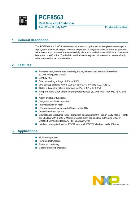
1. General description<br />
2. Features<br />
3. Applications<br />
<strong>PCF8563</strong><br />
<strong>Real</strong> <strong>time</strong> <strong>clock</strong>/<strong>calendar</strong><br />
Rev. 05 — 17 July 2007 Product data sheet<br />
The <strong>PCF8563</strong> is a CMOS real <strong>time</strong> <strong>clock</strong>/<strong>calendar</strong> optimized for low power consumption.<br />
A programmable <strong>clock</strong> output, interrupt output and voltage-low detector are also provided.<br />
All address and data are transferred serially via a two-line bidirectional I 2 C-bus. Maximum<br />
bus speed is 400 kbit/s. The built-in word address register is incremented automatically<br />
after each written or read data byte.<br />
■ Provides year, month, day, weekday, hours, minutes and seconds based on<br />
32.768 kHz quartz crystal<br />
■ Century flag<br />
■ Clock operating voltage: 1.8 V to 5.5 V<br />
■ Low backup current; typical 0.25 μA at VDD = 3.0 V and Tamb =25°C<br />
■ 400 kHz two-wire I 2 C-bus interface (at VDD = 1.8 V to 5.5 V)<br />
■ Programmable <strong>clock</strong> output for peripheral devices (32.768 kHz, 1024 Hz, 32 Hz and<br />
1 Hz)<br />
■ Alarm and <strong>time</strong>r functions<br />
■ Integrated oscillator capacitor<br />
■ Internal power-on reset<br />
■ I 2 C-bus slave address: read A3h and write A2h<br />
■ Open-drain interrupt pin<br />
■ ElectroStatic Discharge (ESD) protection exceeds 2000 V Human Body Model (HBM)<br />
per JESD22-A114, 200 V Machine Model (MM) per JESD22-A115 and 2000 V<br />
Charged Device Model (CDM) per JESD22-C101<br />
■ Latch-up testing is done to JEDEC standard JESD78 which exceeds 100 mA<br />
■ Mobile telephones<br />
■ Portable instruments<br />
■ Electronic metering<br />
■ Battery powered products
NXP Semiconductors <strong>PCF8563</strong><br />
4. Ordering information<br />
5. Block diagram<br />
<strong>Real</strong> <strong>time</strong> <strong>clock</strong>/<strong>calendar</strong><br />
Table 1. Ordering information<br />
Type number Topside Package<br />
mark<br />
Name Description Version<br />
<strong>PCF8563</strong>P <strong>PCF8563</strong>P DIP8 plastic dual in-line package; 8 leads (300 mil) SOT97-1<br />
<strong>PCF8563</strong>T 8563T SO8 plastic small outline package; 8 leads; body width 3.9 mm SOT96-1<br />
<strong>PCF8563</strong>TS 8563 TSSOP8 plastic thin shrink small outline package; 8 leads; body width<br />
3mm<br />
SOT505-1<br />
<strong>PCF8563</strong>BS 8563S HVSON10 plastic thermal enhanced very thin small outline package;<br />
no leads; 10 terminals; body 3 x 3 x 0.85 mm<br />
SOT650-1<br />
OSCI<br />
OSCO<br />
INT<br />
V SS<br />
V DD<br />
SCL<br />
SDA<br />
Fig 1. Block diagram<br />
1<br />
2<br />
3<br />
4<br />
8<br />
6<br />
5<br />
OSCILLATOR<br />
32.768 kHz<br />
VOLTAGE<br />
DETECTOR<br />
OSCILLATOR<br />
MONITOR<br />
I 2 C-BUS<br />
INTERFACE<br />
CONTROL/STATUS 1<br />
CONTROL/STATUS 2<br />
SECONDS/VL<br />
MINUTES<br />
HOURS<br />
<strong>PCF8563</strong>_5 © NXP B.V. 2007. All rights reserved.<br />
Product data sheet Rev. 05 — 17 July 2007 2 of 32<br />
POR<br />
<strong>PCF8563</strong><br />
DIVIDER<br />
CONTROL<br />
LOGIC<br />
ADDRESS<br />
REGISTER<br />
CLKOUT<br />
7<br />
1 Hz<br />
DAYS<br />
WEEKDAYS<br />
MONTHS/CENTURY<br />
YEARS<br />
MINUTE ALARM<br />
HOUR ALARM<br />
DAY ALARM<br />
WEEKDAY ALARM<br />
CLKOUT CONTROL<br />
TIMER CONTROL<br />
TIMER<br />
0<br />
1<br />
2<br />
3<br />
4<br />
5<br />
6<br />
7<br />
8<br />
9<br />
A<br />
B<br />
C<br />
D<br />
E<br />
F<br />
mgm662
NXP Semiconductors <strong>PCF8563</strong><br />
6. Pinning information<br />
6.1 Pinning<br />
OSCI 1<br />
8 VDD<br />
OSCO 2<br />
<strong>PCF8563</strong>P<br />
7 CLKOUT<br />
INT 3<br />
6 SCL<br />
VSS<br />
4<br />
001aaf977<br />
SDA<br />
Fig 2. Pin configuration DIP8 Fig 3. Pin configuration SO8<br />
OSCI 1<br />
8 VDD<br />
OSCO<br />
INT<br />
2<br />
3<br />
<strong>PCF8563</strong>TS<br />
7<br />
6<br />
CLKOUT<br />
SCL<br />
VSS 4<br />
5 SDA<br />
<strong>Real</strong> <strong>time</strong> <strong>clock</strong>/<strong>calendar</strong><br />
Fig 4. Pin configuration TSSOP8 Fig 5. Pin configuration HVSON10<br />
Fig 6. Device diode protection diagram<br />
5<br />
001aaf976<br />
OSCI<br />
OSCO<br />
INT<br />
VSS<br />
OSCI 1<br />
8 VDD<br />
OSCO 2<br />
<strong>PCF8563</strong>T<br />
7 CLKOUT<br />
INT 3<br />
6 SCL<br />
<strong>PCF8563</strong>_5 © NXP B.V. 2007. All rights reserved.<br />
Product data sheet Rev. 05 — 17 July 2007 3 of 32<br />
VSS<br />
terminal 1<br />
index area<br />
1 8<br />
2 7<br />
3 6<br />
4 5<br />
<strong>PCF8563</strong><br />
4<br />
001aaf975<br />
5<br />
SDA<br />
OSCI 1 10 n.c.<br />
OSCO 2 9 VDD<br />
mgr886<br />
n.c. 3 <strong>PCF8563</strong>BS 8 CLKOUT<br />
INT<br />
VSS<br />
4 7<br />
5 6<br />
VDD<br />
CLKOUT<br />
SCL<br />
SDA<br />
Transparent top view<br />
001aaf981<br />
SCL<br />
SDA
NXP Semiconductors <strong>PCF8563</strong><br />
6.2 Pin description<br />
7. Functional description<br />
<strong>Real</strong> <strong>time</strong> <strong>clock</strong>/<strong>calendar</strong><br />
Table 2. Pin description<br />
Symbol Pin Description<br />
DIP8, SO8,<br />
TSSOP8<br />
HVSON10<br />
OSCI 1 1 oscillator input<br />
OSCO 2 2 oscillator output<br />
n.c - 3 not connected<br />
INT 3 4 interrupt output (open-drain; active LOW)<br />
VSS 4 5 ground<br />
SDA 5 6 serial data input and output<br />
SCL 6 7 serial <strong>clock</strong> input<br />
CLKOUT 7 8 <strong>clock</strong> output, open-drain<br />
VDD 8 9 positive supply voltage<br />
n.c - 10 not connected<br />
The <strong>PCF8563</strong> contains sixteen 8-bit registers with an auto-incrementing address register,<br />
an on-chip 32.768 kHz oscillator with one integrated capacitor, a frequency divider which<br />
provides the source <strong>clock</strong> for the <strong>Real</strong> Time Clock/calender (RTC), a programmable <strong>clock</strong><br />
output, a <strong>time</strong>r, an alarm, a voltage-low detector and a 400 kHz I 2 C-bus interface.<br />
All 16 registers are designed as addressable 8-bit parallel registers although not all bits<br />
are implemented. The first two registers (memory address 00h and 01h) are used as<br />
control and/or status registers. The memory addresses 02h through 08h are used as<br />
counters for the <strong>clock</strong> function (seconds up to years counters). Address locations 09h<br />
through 0Ch contain alarm registers which define the conditions for an alarm.<br />
Address 0Dh controls the CLKOUT output frequency. 0Eh and 0Fh are the <strong>time</strong>r control<br />
and <strong>time</strong>r registers, respectively.<br />
The seconds, minutes, hours, days, weekdays, months, years as well as the minute alarm,<br />
hour alarm, day alarm and weekday alarm registers are all coded in Binary Coded<br />
Decimal (BCD) format.<br />
When one of the RTC registers is read the contents of all counters are frozen. Therefore,<br />
faulty reading of the <strong>clock</strong>/<strong>calendar</strong> during a carry condition is prevented.<br />
7.1 Alarm function modes<br />
By clearing the MSB of one or more of the alarm registers (bit AE = alarm enable), the<br />
corresponding alarm condition(s) will be active. In this way an alarm can be generated<br />
from once per minute up to once per week. The alarm condition sets the Alarm Flag (AF).<br />
The asserted AF can be used to generate an interrupt (INT). The AF can only be cleared<br />
by software.<br />
<strong>PCF8563</strong>_5 © NXP B.V. 2007. All rights reserved.<br />
Product data sheet Rev. 05 — 17 July 2007 4 of 32
NXP Semiconductors <strong>PCF8563</strong><br />
7.2 Timer<br />
<strong>Real</strong> <strong>time</strong> <strong>clock</strong>/<strong>calendar</strong><br />
The 8-bit countdown <strong>time</strong>r at address 0Fh is controlled by the <strong>time</strong>r control register at<br />
address 0Eh. The <strong>time</strong>r control register determines one of 4 source <strong>clock</strong> frequencies for<br />
the <strong>time</strong>r (4096 Hz, 64 Hz, 1 Hz, or 1 ⁄60 Hz), and enables or disables the <strong>time</strong>r. The <strong>time</strong>r<br />
counts down from a software-loaded 8-bit binary value. At the end of every countdown,<br />
the <strong>time</strong>r sets the Timer Flag (TF). The TF may only be cleared by software. The<br />
asserted TF can be used to generate an interrupt (INT). The interrupt may be generated<br />
as a pulsed signal every countdown period or as a permanently active signal which<br />
follows the condition of TF. Bit TI/TP is used to control this mode selection. When reading<br />
the <strong>time</strong>r, the current countdown value is returned.<br />
7.3 Clock output<br />
A programmable square wave is available at pin CLKOUT. Operation is controlled by the<br />
CLKOUT control register at address 0Dh. Frequencies of 32.768 kHz (default), 1024 Hz,<br />
32 Hz and 1 Hz can be generated for use as a system <strong>clock</strong>, microcontroller <strong>clock</strong>, input to<br />
a charge pump, or for calibration of the oscillator. CLKOUT is an open-drain output and<br />
enabled at power-on. If disabled it becomes high-impedance.<br />
7.4 Reset<br />
The <strong>PCF8563</strong> includes an internal reset circuit which is active whenever the oscillator is<br />
stopped. In the reset state the I 2 C-bus logic is initialized and all registers are reset<br />
according to Table 25.<br />
7.5 Voltage-low detector<br />
The <strong>PCF8563</strong> has an on-chip voltage-low detector (see Figure 7). When VDD drops below<br />
Vlow, bit VL in the seconds register is set to indicate that the integrity of the <strong>clock</strong><br />
information is no longer guaranteed. The VL flag can only be cleared by software.<br />
Bit VL is intended to detect the situation when VDD is decreasing slowly, for example under<br />
battery operation. Should VDD reach Vlow before power is re-asserted then bit VL is set.<br />
This will indicate that the <strong>time</strong> may be corrupted.<br />
VDD<br />
Vlow<br />
Fig 7. Voltage-low detection<br />
period of battery<br />
operation<br />
<strong>PCF8563</strong>_5 © NXP B.V. 2007. All rights reserved.<br />
Product data sheet Rev. 05 — 17 July 2007 5 of 32<br />
VL set<br />
mgr887<br />
normal power<br />
operation<br />
t
NXP Semiconductors <strong>PCF8563</strong><br />
7.6 Register organization<br />
7.6.1 Control/status 1 register<br />
7.6.2 Control/status 2 register<br />
<strong>Real</strong> <strong>time</strong> <strong>clock</strong>/<strong>calendar</strong><br />
Table 3. Formatted registers overview<br />
Bit positions labelled as x are not implemented. Bit positions labelled with 0 should always be written with logic 0; if read they<br />
could be either logic 0 or logic 1.<br />
Address Register name Bit 7 Bit 6 Bit 5 Bit 4 Bit 3 Bit 2 Bit 1 Bit 0<br />
00h control/status 1 TEST1 0 STOP 0 TESTC 0 0 0<br />
01h control/status 2 0 0 0 TI/TP AF TF AIE TIE<br />
02h seconds VL <br />
03h minutes x <br />
04h hours x x <br />
05h days x x <br />
06h weekdays x x x x x <br />
07h months/century C x x <br />
08h years <br />
09h minute alarm AE <br />
0Ah hour alarm AE x <br />
0Bh day alarm AE x <br />
0Ch weekday alarm AE x x x x <br />
0Dh CLKOUT control FE x x x x x FD1 FD0<br />
0Eh <strong>time</strong>r control AT x x x x x TD1 TD0<br />
0Fh <strong>time</strong>r <br />
Table 4. Control/status 1 (address 00h) bits description<br />
Bit Symbol Value Description<br />
7 TEST1 0 normal mode<br />
1 EXT_CLK test mode<br />
6 0 default value is logic 0<br />
5 STOP 0 RTC source <strong>clock</strong> runs<br />
1 all RTC divider chain flip-flops are asynchronously set to logic 0;<br />
the RTC <strong>clock</strong> is stopped (CLKOUT at 32.768 kHz is still<br />
available)<br />
4 0 default value is logic 0<br />
3 TESTC 0 Power-on reset override facility is disabled; set to logic 0 for<br />
normal operation<br />
1 Power-on reset override may be enabled<br />
2 to 0 0 default value is logic 0<br />
Bits TF and AF: When an alarm occurs, AF is set to logic 1. Similarly, at the end of a <strong>time</strong>r<br />
countdown, TF is set to logic 1. These bits maintain their value until overwritten by<br />
software. If both <strong>time</strong>r and alarm interrupts are required in the application, the source of<br />
the interrupt can be determined by reading these bits. To prevent one flag being<br />
overwritten while clearing another a logic AND is performed during a write access.<br />
<strong>PCF8563</strong>_5 © NXP B.V. 2007. All rights reserved.<br />
Product data sheet Rev. 05 — 17 July 2007 6 of 32
NXP Semiconductors <strong>PCF8563</strong><br />
<strong>Real</strong> <strong>time</strong> <strong>clock</strong>/<strong>calendar</strong><br />
Bits TIE and AIE: These bits activate or deactivate the generation of an interrupt when<br />
TF or AF is asserted, respectively. The interrupt is the logical OR of these two conditions<br />
when both AIE and TIE are set.<br />
Table 5. Control/status 2 (address 01h) bits description<br />
Bit Symbol Value Description<br />
7 to 5 0 default value is logic 0<br />
4 TI/TP 0 INT is active when TF is active (subject to the status of TIE)<br />
1 INT pulses active according to Table 6 (subject to the status of<br />
TIE); note that if AF and AIE are active then INT will be<br />
permanently active<br />
3 AF 0 (read) alarm flag inactive<br />
1 (read) alarm flag active<br />
0 (write) alarm flag is cleared<br />
1 (write) alarm flag remains unchanged<br />
2 TF 0 (read) <strong>time</strong>r flag inactive<br />
1 (read) <strong>time</strong>r flag active<br />
0 (write) <strong>time</strong>r flag is cleared<br />
1 (write) <strong>time</strong>r flag remains unchanged<br />
1 AIE 0 alarm interrupt disabled<br />
1 alarm interrupt enabled<br />
0 TIE 0 <strong>time</strong>r interrupt disabled<br />
1 <strong>time</strong>r interrupt enabled<br />
Table 6. INT operation (bit TI/TP = 1)<br />
Source <strong>clock</strong> (Hz) INT period (s) [1]<br />
n=1 [2] n>1<br />
4096 1⁄8192 1⁄4096<br />
64 1⁄128 1⁄64<br />
1 1⁄64 1⁄64<br />
1⁄60 1⁄64 1⁄64<br />
[1] TF and INT become active simultaneously.<br />
[2] n = loaded countdown value. Timer stopped when n = 0.<br />
7.6.3 Time and date registers<br />
Table 7. Seconds/VL (address 02h) bits description<br />
Bit Symbol Value Description<br />
7 VL 0 <strong>clock</strong> integrity is guaranteed<br />
1 integrity of the <strong>clock</strong> information is no longer guaranteed<br />
6 to 0 SECONDS 00 to 59 this register holds the current seconds coded in BCD format;<br />
example: seconds register contains x101 1001 = 59 seconds<br />
Table 8. Minutes (address 03h) bits description<br />
Bit Symbol Value Description<br />
6 to 0 MINUTES 00 to 59 this register holds the current minutes coded in BCD format<br />
<strong>PCF8563</strong>_5 © NXP B.V. 2007. All rights reserved.<br />
Product data sheet Rev. 05 — 17 July 2007 7 of 32
NXP Semiconductors <strong>PCF8563</strong><br />
Table 9. Hours (address 04h) bits description<br />
<strong>Real</strong> <strong>time</strong> <strong>clock</strong>/<strong>calendar</strong><br />
Bit Symbol Value Description<br />
5 to 0 HOURS 00 to 23 this register holds the current hours coded in BCD format<br />
Table 10. Days (address 05h) bits description<br />
Bit Symbol Value Description<br />
5 to 0 DAYS 01 to 31 [1] this register holds the current day coded in BCD format<br />
[1] The <strong>PCF8563</strong> compensates for leap years by adding a 29th day to February if the year counter contains a<br />
value which is exactly divisible by 4, including the year 00.<br />
Table 11. Weekdays (address 06h) bits description<br />
Bit Symbol Value Description<br />
2 to 0 WEEKDAYS 0 to 6 [1] this register holds the current weekday coded in BCD<br />
format, see Table 12<br />
[1] These bits may be re-assigned by the user.<br />
Table 12. Weekday assignments<br />
Day Bit 7 Bit 6 Bit 5 Bit 4 Bit 3 Bit 2 Bit 1 Bit 0<br />
Sunday x x x x x 0 0 0<br />
Monday x x x x x 0 0 1<br />
Tuesday x x x x x 0 1 0<br />
Wednesday x x x x x 0 1 1<br />
Thursday x x x x x 1 0 0<br />
Friday x x x x x 1 0 1<br />
Saturday x x x x x 1 1 0<br />
Table 13. Months/century (address 07h) bits description<br />
Bit Symbol Value Description<br />
7 CENTURY [1] this bit is toggled when the years register overflows from<br />
99 to 00<br />
0 indicates the century is 20xx<br />
1 indicates the century is 19xx<br />
4 to 0 MONTH 01 to 12 this register holds the current month coded in BCD format,<br />
see Table 14<br />
[1] These bits may be re-assigned by the user.<br />
Table 14. Month assignments<br />
Month Bit 7 Bit 6 Bit 5 Bit 4 Bit 3 Bit 2 Bit 1 Bit 0<br />
January C x x 0 0 0 0 1<br />
February C x x 0 0 0 1 0<br />
March C x x 0 0 0 1 1<br />
April C x x 0 0 1 0 0<br />
May C x x 0 0 1 0 1<br />
June C x x 0 0 1 1 0<br />
<strong>PCF8563</strong>_5 © NXP B.V. 2007. All rights reserved.<br />
Product data sheet Rev. 05 — 17 July 2007 8 of 32
NXP Semiconductors <strong>PCF8563</strong><br />
7.6.4 Alarm registers<br />
<strong>Real</strong> <strong>time</strong> <strong>clock</strong>/<strong>calendar</strong><br />
Table 14. Month assignments …continued<br />
Month Bit 7 Bit 6 Bit 5 Bit 4 Bit 3 Bit 2 Bit 1 Bit 0<br />
July C x x 0 0 1 1 1<br />
August C x x 0 1 0 0 0<br />
September C x x 0 1 0 0 1<br />
October C x x 1 0 0 0 0<br />
November C x x 1 0 0 0 1<br />
December C x x 1 0 0 1 0<br />
Table 15. Years (address 08h) bits description<br />
Bit Symbol Value Description<br />
7 to 0 YEARS 00 to 99 this register holds the current year coded in BCD format<br />
When one or more of these registers are loaded with a valid minute, hour, day or weekday<br />
and its corresponding bit Alarm Enable (AE) is logic 0, then that information will be<br />
compared with the current minute, hour, day and weekday. When all enabled comparisons<br />
first match, the Alarm Flag (AF) is set. AF will remain set until cleared by software.<br />
Once AF has been cleared it will only be set again when the <strong>time</strong> increments to match the<br />
alarm condition once more. Alarm registers which have their bit AE at logic 1 will be<br />
ignored.<br />
Table 16. Minute alarm (address 09h) bits description<br />
Bit Symbol Value Description<br />
7 AE 0 minute alarm is enabled<br />
1 minute alarm is disabled<br />
6 to 0 ALARM 00 to 59 this register holds the minute alarm information coded in BCD<br />
_MINUTES<br />
format<br />
Table 17. Hour alarm (address 0Ah) bits description<br />
Bit Symbol Value Description<br />
7 AE 0 hour alarm is enabled<br />
1 hour alarm is disabled<br />
5 to 0 ALARM_ 00 to 23 this register holds the hour alarm information coded in BCD<br />
HOURS<br />
format<br />
Table 18. Day alarm (address 0Bh) bits description<br />
Bit Symbol Value Description<br />
7 AE 0 day alarm is enabled<br />
1 day alarm is disabled<br />
5 to 0 ALARM_<br />
DAYS<br />
01 to 31 this register holds the day alarm information coded in BCD format<br />
<strong>PCF8563</strong>_5 © NXP B.V. 2007. All rights reserved.<br />
Product data sheet Rev. 05 — 17 July 2007 9 of 32
NXP Semiconductors <strong>PCF8563</strong><br />
7.6.5 Clock output control register<br />
7.6.6 Countdown <strong>time</strong>r<br />
<strong>Real</strong> <strong>time</strong> <strong>clock</strong>/<strong>calendar</strong><br />
Table 19. Weekday alarm (address 0Ch) bits description<br />
Bit Symbol Value Description<br />
7 AE 0 weekday alarm is enabled<br />
1 weekday alarm is disabled<br />
2 to 0 ALARM_ 0 to 6 this register holds the weekday alarm information coded in<br />
WEEKDAYS<br />
BCD format<br />
Table 20. CLKOUT control (address 0Dh) bits description<br />
Bit Symbol Value Description<br />
7 FE 0 the CLKOUT output is inhibited and CLKOUT output is set to<br />
high-impedance<br />
1 the CLKOUT output is activated<br />
1 to 0 FD1 and<br />
these bits control the frequency output at pin CLKOUT;<br />
FD0<br />
see Table 21<br />
Table 21. FD1 and FD0: CLKOUT frequency selection<br />
FD1 FD0 CLKOUT frequency<br />
0 0 32.768 kHz<br />
0 1 1024 Hz<br />
1 0 32 Hz<br />
1 1 1 Hz<br />
The <strong>time</strong>r register is an 8-bit binary countdown <strong>time</strong>r. It is enabled and disabled via the<br />
<strong>time</strong>r control register bit TE. The source <strong>clock</strong> for the <strong>time</strong>r is also selected by the <strong>time</strong>r<br />
control register. Other <strong>time</strong>r properties such as interrupt generation are controlled via<br />
control/status 2 register.<br />
For accurate read back of the countdown value, the I 2 C-bus <strong>clock</strong> (SCL) must be<br />
operating at a frequency of at least twice the selected <strong>time</strong>r <strong>clock</strong>.<br />
Table 22. Timer control (address 0Eh) bits description<br />
Bit Symbol Value Description<br />
7 TE 0 <strong>time</strong>r is disabled<br />
1 <strong>time</strong>r is enabled<br />
1 to 0 TD1 and<br />
TD0<br />
<strong>time</strong>r source <strong>clock</strong> frequency select; these bits determine the<br />
source <strong>clock</strong> for the countdown <strong>time</strong>r, see Table 23; when not in<br />
use, TD1 and TD0 should be set to 1 ⁄60 Hz for power saving<br />
Table 23. TD1 and TD0: Timer frequency selection<br />
TD1 TD0 TIMER Source <strong>clock</strong> frequency<br />
0 0 4096 Hz<br />
0 1 64 Hz<br />
1 0 1 Hz<br />
1 1 1⁄60 Hz<br />
<strong>PCF8563</strong>_5 © NXP B.V. 2007. All rights reserved.<br />
Product data sheet Rev. 05 — 17 July 2007 10 of 32
NXP Semiconductors <strong>PCF8563</strong><br />
Table 24. Timer (address 0Fh) bits description<br />
Bit Symbol Value Description<br />
7 to 0 TIMER 00h to FFh countdown value = n;<br />
CountdownPeriod =<br />
n<br />
--------------------------------------------------------------<br />
SourceClockFrequency<br />
7.7 EXT_CLK test mode<br />
<strong>Real</strong> <strong>time</strong> <strong>clock</strong>/<strong>calendar</strong><br />
A test mode is available which allows for on-board testing. In such a mode it is possible to<br />
set up test conditions and control the operation of the RTC.<br />
The test mode is entered by setting bit TEST1 in control/status1 register. Then<br />
pin CLKOUT becomes an input. The test mode replaces the internal 64 Hz signal with the<br />
signal applied to pin CLKOUT. Every 64 positive edges applied to pin CLKOUT will then<br />
generate an increment of one second.<br />
The signal applied to pin CLKOUT should have a minimum pulse width of 300 ns and a<br />
minimum period of 1000 ns. The internal 64 Hz <strong>clock</strong>, now sourced from CLKOUT, is<br />
divided down to 1 Hz by a 2 6 divide chain called a pre-scaler. The pre-scaler can be set<br />
into a known state by using bit STOP. When bit STOP is set, the pre-scaler is reset to 0<br />
(STOP must be cleared before the pre-scaler can operate again).<br />
From a STOP condition, the first 1 second increment will take place after 32 positive<br />
edges on CLKOUT. Thereafter, every 64 positive edges will cause a 1 second increment.<br />
Remark: Entry into EXT_CLK test mode is not synchronized to the internal 64 Hz <strong>clock</strong>.<br />
When entering the test mode, no assumption as to the state of the pre-scaler can be<br />
made.<br />
Operation example:<br />
1. Set EXT_CLK test mode (control/status 1, bit TEST1 = 1)<br />
2. Set STOP (control/status 1, bit STOP = 1)<br />
3. Clear STOP (control/status 1, bit STOP = 0)<br />
4. Set <strong>time</strong> registers to desired value<br />
5. Apply 32 <strong>clock</strong> pulses to CLKOUT<br />
6. Read <strong>time</strong> registers to see the first change<br />
7. Apply 64 <strong>clock</strong> pulses to CLKOUT<br />
8. Read <strong>time</strong> registers to see the second change<br />
Repeat 7 and 8 for additional increments.<br />
7.8 Power-On Reset (POR) override<br />
The POR duration is directly related to the crystal oscillator start-up <strong>time</strong>. Due to the long<br />
start-up <strong>time</strong>s experienced by these types of circuits, a mechanism has been built in to<br />
disable the POR and hence speed up on-board test of the device. The setting of this mode<br />
requires that the I2C-bus pins, SDA and SCL, be toggled in a specific order as shown in<br />
Figure 8. All timings are required minimums.<br />
<strong>PCF8563</strong>_5 © NXP B.V. 2007. All rights reserved.<br />
Product data sheet Rev. 05 — 17 July 2007 11 of 32
NXP Semiconductors <strong>PCF8563</strong><br />
SDA<br />
SCL<br />
8 ms<br />
power up<br />
Fig 8. POR override sequence<br />
<strong>Real</strong> <strong>time</strong> <strong>clock</strong>/<strong>calendar</strong><br />
Once the override mode has been entered, the device immediately stops being reset and<br />
normal operation may commence i.e. entry into the EXT_CLK test mode via I 2 C-bus<br />
access. The override mode may be cleared by writing a logic 0 to TESTC. TESTC must be<br />
set to logic 1 before re-entry into the override mode is possible. Setting TESTC to logic 0<br />
during normal operation has no effect except to prevent entry into the POR override mode.<br />
500 ns 2000 ns<br />
Table 25 shows the register reset values.<br />
[1] registers marked ‘x’ are undefined at power-up and unchanged by subsequent resets.<br />
8. Characteristics of the I 2 C-bus<br />
override active<br />
The I 2 C-bus is for bidirectional, two-line communication between different ICs or modules.<br />
The two lines are a serial data line (SDA) and a serial <strong>clock</strong> line (SCL). Both lines must be<br />
connected to a positive supply via a pull-up resistor. Data transfer may be initiated only<br />
when the bus is not busy.<br />
<strong>PCF8563</strong>_5 © NXP B.V. 2007. All rights reserved.<br />
Product data sheet Rev. 05 — 17 July 2007 12 of 32<br />
mgm664<br />
Table 25: Register reset value [1]<br />
Address Register name Bit 7 Bit 6 Bit 5 Bit 4 Bit 3 Bit 2 Bit 1 Bit 0<br />
00h control/status 1 0 0 0 0 1 0 0 0<br />
01h control/status 2 x x 0 0 0 0 0 0<br />
02h seconds 1 x x x x x x x<br />
03h minutes 1 x x x x x x x<br />
04h hours x x x x x x x x<br />
05h days x x x x x x x x<br />
06h weekdays x x x x x x x x<br />
07h months/century x x x x x x x x<br />
08h years x x x x x x x x<br />
09h minute alarm 1 x x x x x x x<br />
0Ah hour alarm 1 x x x x x x x<br />
0Bh day alarm 1 x x x x x x x<br />
0Ch weekday alarm 1 x x x x x x x<br />
0Dh CLKOUT control 1 x x x x x 0 0<br />
0Eh <strong>time</strong>r control 0 x x x x x 1 1<br />
0Fh <strong>time</strong>r x x x x x x x x
NXP Semiconductors <strong>PCF8563</strong><br />
SDA<br />
SCL<br />
8.1 Bit transfer<br />
<strong>Real</strong> <strong>time</strong> <strong>clock</strong>/<strong>calendar</strong><br />
One data bit is transferred during each <strong>clock</strong> pulse. The data on the SDA line must remain<br />
stable during the HIGH period of the <strong>clock</strong> pulse as changes in the data line at this <strong>time</strong><br />
will be interpreted as a control signal (see Figure 9).<br />
Fig 9. Bit transfer<br />
8.2 Start and stop conditions<br />
Both data and <strong>clock</strong> lines remain HIGH when the bus is not busy. A HIGH-to-LOW<br />
transition of the data line, while the <strong>clock</strong> is HIGH is defined as the START condition (S). A<br />
LOW-to-HIGH transition of the data line while the <strong>clock</strong> is HIGH is defined as the STOP<br />
condition (P); see Figure 10.<br />
8.3 System configuration<br />
MASTER<br />
TRANSMITTER /<br />
RECEIVER<br />
Fig 11. System configuration<br />
SDA<br />
SCL<br />
SDA<br />
SCL<br />
S<br />
START condition<br />
data line<br />
stable;<br />
data valid<br />
Fig 10. Definition of start and stop conditions<br />
change<br />
of data<br />
allowed<br />
A device generating a message is a transmitter, a device receiving a message is the<br />
receiver. The device that controls the message is the master and the devices which are<br />
controlled by the master are the slaves (see Figure 11).<br />
SLAVE<br />
RECEIVER<br />
SLAVE<br />
TRANSMITTER /<br />
RECEIVER<br />
MASTER<br />
TRANSMITTER<br />
<strong>PCF8563</strong>_5 © NXP B.V. 2007. All rights reserved.<br />
Product data sheet Rev. 05 — 17 July 2007 13 of 32<br />
mbc621<br />
P<br />
STOP condition<br />
MASTER<br />
TRANSMITTER /<br />
RECEIVER<br />
mba605<br />
SDA<br />
SCL<br />
mbc622
NXP Semiconductors <strong>PCF8563</strong><br />
8.4 Acknowledge<br />
<strong>Real</strong> <strong>time</strong> <strong>clock</strong>/<strong>calendar</strong><br />
The number of data bytes transferred between the START and STOP conditions from<br />
transmitter to receiver is unlimited. Each byte of eight bits is followed by an acknowledge<br />
bit. The acknowledge bit is a HIGH-level signal put on the bus by the transmitter during<br />
which <strong>time</strong> the master generates an extra acknowledge related <strong>clock</strong> pulse. A slave<br />
receiver which is addressed must generate an acknowledge after the reception of each<br />
byte. Also a master receiver must generate an acknowledge after the reception of each<br />
byte that has been <strong>clock</strong>ed out of the slave transmitter (see Figure 12).<br />
The device that acknowledges must pull down the SDA line during the acknowledge <strong>clock</strong><br />
pulse, so that the SDA line is stable LOW during the HIGH period of the acknowledge<br />
related <strong>clock</strong> pulse (set-up and hold <strong>time</strong>s must be taken into consideration). A master<br />
receiver must signal an end of data to the transmitter by not generating an acknowledge<br />
on the last byte that has been <strong>clock</strong>ed out of the slave. In this event the transmitter must<br />
leave the data line HIGH to enable the master to generate a stop condition.<br />
data output<br />
by transmitter<br />
data output<br />
by receiver<br />
SCL from<br />
master<br />
Fig 12. Acknowledgement on the I 2 C-bus<br />
8.5 I 2 C-bus protocol<br />
8.5.1 Addressing<br />
S<br />
START<br />
condition<br />
Before any data is transmitted on the I 2 C-bus, the device which should respond is<br />
addressed first. The addressing is always carried out with the first byte transmitted after<br />
the start procedure.<br />
The <strong>PCF8563</strong> acts as a slave receiver or slave transmitter. Therefore the <strong>clock</strong> signal SCL<br />
is only an input signal, but the data signal SDA is a bidirectional line.<br />
The <strong>PCF8563</strong> slave address is shown in Figure 13.<br />
Fig 13. Slave address<br />
<strong>PCF8563</strong>_5 © NXP B.V. 2007. All rights reserved.<br />
Product data sheet Rev. 05 — 17 July 2007 14 of 32<br />
1<br />
1 0 1 0 0 0 1 R/W<br />
group 1 group 2<br />
2<br />
mce189<br />
not acknowledge<br />
acknowledge<br />
8<br />
9<br />
<strong>clock</strong> pulse for<br />
acknowledgement<br />
mbc602
NXP Semiconductors <strong>PCF8563</strong><br />
8.5.2 Clock/<strong>calendar</strong> read/write cycles<br />
<strong>Real</strong> <strong>time</strong> <strong>clock</strong>/<strong>calendar</strong><br />
The I 2 C-bus configuration for the different <strong>PCF8563</strong> read and write cycles is shown in<br />
Figure 14, Figure 15 and Figure 16. The word address is a 4-bit value that defines which<br />
register is to be accessed next. The upper four bits of the word address are not used.<br />
acknowledgement<br />
from slave<br />
acknowledgement<br />
from slave<br />
S SLAVE ADDRESS 0 A WORD ADDRESS A DATA A P<br />
R/W<br />
Fig 14. Master transmits to slave receiver (write mode)<br />
acknowledgement<br />
from slave<br />
S SLAVE ADDRESS 0 A WORD ADDRESS A S SLAVE ADDRESS 1 A<br />
R/W<br />
acknowledgement<br />
from slave<br />
at this moment master transmitter<br />
becomes master receiver and<br />
PCA8563 slave receiver<br />
becomes slave transmitter<br />
Fig 15. Master reads after setting word address (write word address; read data)<br />
acknowledgement<br />
from slave<br />
acknowledgement<br />
from slave<br />
acknowledgement<br />
from slave<br />
auto increment<br />
memory word address<br />
<strong>PCF8563</strong>_5 © NXP B.V. 2007. All rights reserved.<br />
Product data sheet Rev. 05 — 17 July 2007 15 of 32<br />
n bytes<br />
DATA<br />
DATA<br />
last byte<br />
S SLAVE ADDRESS 1 A DATA A DATA 1<br />
Fig 16. Master reads slave immediately after first byte (read mode)<br />
R/W<br />
acknowledgement<br />
from master<br />
R/W<br />
n bytes last byte<br />
auto increment<br />
word address<br />
n bytes<br />
no acknowledgement<br />
from master<br />
auto increment<br />
word address<br />
mbd822<br />
acknowledgement<br />
from master<br />
A<br />
auto increment<br />
memory word address<br />
no acknowledgement<br />
from master<br />
1<br />
P<br />
auto increment<br />
memory word address<br />
P<br />
mgl665<br />
001aag133
NXP Semiconductors <strong>PCF8563</strong><br />
9. Limiting values<br />
10. Static characteristics<br />
Table 26. Limiting values<br />
In accordance with the Absolute Maximum Rating System (IEC 60134)<br />
<strong>Real</strong> <strong>time</strong> <strong>clock</strong>/<strong>calendar</strong><br />
Symbol Parameter Min Max Unit<br />
VDD supply voltage −0.5 +6.5 V<br />
IDD supply current −50 +50 mA<br />
VI input voltage on pins SCL and SDA −0.5 +6.5 V<br />
input voltage on pin OSCI −0.5 VDD + 0.5 V<br />
VO<br />
output voltage on pins CLOCKOUT<br />
and INT<br />
−0.5 +6.5 V<br />
II DC input current at any input −10 +10 mA<br />
IO DC output current at any output −10 +10 mA<br />
Ptot total power dissipation - 300 mW<br />
Tamb ambient temperature −40 +85 °C<br />
Tstg storage temperature −65 +150 °C<br />
Table 27. Static characteristics<br />
VDD = 1.8 V to 5.5 V; VSS =0V; Tamb = −40 °C to +85 °C; fosc = 32.768 kHz; quartz Rs =40kΩ; CL = 8 pF; unless otherwise<br />
specified.<br />
Symbol<br />
Supplies<br />
Parameter Conditions Min Typ Max Unit<br />
VDD supply voltage interface inactive; fSCL = 0 Hz;<br />
Tamb =25°C; see Figure 20<br />
[1] 1.0 - 5.5 V<br />
interface active;<br />
fSCL = 400 kHz; see Figure 20<br />
[1] 1.8 - 5.5 V<br />
<strong>clock</strong> data integrity;<br />
Tamb =25°C<br />
Vlow - 5.5 V<br />
IDD1 supply current 1 interface active; see Figure 19<br />
fSCL = 400 kHz - - 800 μA<br />
fSCL = 100 kHz - - 200 μA<br />
IDD2 supply current 2 interface inactive (fSCL = 0 Hz);<br />
CLKOUT disabled;<br />
Tamb =25°C; see Figure 17<br />
[2]<br />
VDD = 5.0 V - 275 550 nA<br />
VDD = 3.0 V - 250 500 nA<br />
VDD = 2.0 V - 225 450 nA<br />
interface inactive (fSCL = 0 Hz);<br />
CLKOUT disabled;<br />
Tamb = −40 °C to +85 °C;<br />
see Figure 17<br />
[2]<br />
VDD = 5.0 V - 500 750 nA<br />
VDD = 3.0 V - 400 650 nA<br />
VDD = 2.0 V - 400 600 nA<br />
<strong>PCF8563</strong>_5 © NXP B.V. 2007. All rights reserved.<br />
Product data sheet Rev. 05 — 17 July 2007 16 of 32
NXP Semiconductors <strong>PCF8563</strong><br />
IDD3 supply current 3 interface inactive (fSCL = 0 Hz);<br />
CLKOUT enabled at 32 kHz;<br />
Tamb =25°C; see Figure 18<br />
Inputs<br />
[1] For reliable oscillator start-up at power-up: VDD(min)power-up =VDD(min) + 0.3 V.<br />
[2] Timer source <strong>clock</strong> = 1 ⁄60 Hz, level of pins SCL and SDA is VDD or VSS.<br />
[3] Tested on sample basis.<br />
[4] See Figure 7.<br />
<strong>Real</strong> <strong>time</strong> <strong>clock</strong>/<strong>calendar</strong><br />
Table 27. Static characteristics …continued<br />
VDD = 1.8 V to 5.5 V; VSS =0V; Tamb = −40 °C to +85 °C; fosc = 32.768 kHz; quartz Rs =40kΩ; CL = 8 pF; unless otherwise<br />
specified.<br />
Symbol Parameter Conditions Min Typ Max Unit<br />
<strong>PCF8563</strong>_5 © NXP B.V. 2007. All rights reserved.<br />
Product data sheet Rev. 05 — 17 July 2007 17 of 32<br />
[2]<br />
VDD = 5.0 V - 825 1600 nA<br />
VDD = 3.0 V - 550 1000 nA<br />
VDD = 2.0 V - 425 800 nA<br />
interface inactive (fSCL = 0 Hz);<br />
CLKOUT enabled at 32 kHz;<br />
Tamb = −40 °C to +85 °C;<br />
see Figure 18<br />
[2]<br />
VDD = 5.0 V - 950 1700 nA<br />
VDD = 3.0 V - 650 1100 nA<br />
VDD = 2.0 V - 500 900 nA<br />
VIL LOW-level input voltage VSS - 0.3VDD V<br />
VIH HIGH-level input voltage 0.7VDD - VDD V<br />
ILI input leakage current VI =VDD or VSS −1 0 +1 μA<br />
Ci<br />
Outputs<br />
input capacitance [3] - - 7 pF<br />
IOL(SDA) SDA LOW-level output<br />
current<br />
VOL = 0.4 V; VDD =5V −3 - - mA<br />
IOL(INT) INT LOW-level output<br />
current<br />
VOL = 0.4 V; VDD =5V −1 - - mA<br />
IOL(CLKOUT) CLKOUT LOW-level<br />
output current<br />
VOL = 0.4 V; VDD =5V −1 - - mA<br />
IOH(CLKOUT) CLKOUT HIGH-level<br />
output current<br />
VOH = 4.6 V; VDD =5V 1 - - mA<br />
ILO output leakage current VO =VDD or VSS −1 0 +1 μA<br />
Voltage detector<br />
Vlow low voltage detection Tamb =25°C; VL set voltage [4] - 0.9 1.0 V
NXP Semiconductors <strong>PCF8563</strong><br />
IDD<br />
(mA)<br />
1<br />
0.8<br />
0.6<br />
0.4<br />
0.2<br />
mgr888<br />
0<br />
0 2 4<br />
VDD (V)<br />
6<br />
Tamb =25°C; Timer = 1 minute. Tamb =25°C; Timer = 1 minute.<br />
<strong>Real</strong> <strong>time</strong> <strong>clock</strong>/<strong>calendar</strong><br />
0<br />
0 2 4<br />
VDD (V)<br />
6<br />
Fig 17. IDD as a function of VDD; CLKOUT disabled Fig 18. IDD as a function of VDD; CLKOUT = 32 kHz<br />
IDD<br />
(mA)<br />
1<br />
0.8<br />
0.6<br />
0.4<br />
0.2<br />
mgr890<br />
0<br />
−40 0 40 80<br />
T (°C)<br />
120<br />
VDD = 3 V; Timer = 1 minute. Tamb =25°C; normalized to VDD =3V.<br />
Fig 19. IDD as a function of T; CLKOUT = 32 kHz Fig 20. Frequency deviation as a function of VDD<br />
<strong>PCF8563</strong>_5 © NXP B.V. 2007. All rights reserved.<br />
Product data sheet Rev. 05 — 17 July 2007 18 of 32<br />
IDD<br />
(mA)<br />
1<br />
0.8<br />
0.6<br />
0.4<br />
0.2<br />
4<br />
frequency<br />
deviation<br />
(ppm)<br />
2<br />
0<br />
−2<br />
−4<br />
mgr889<br />
mgr891<br />
0 2 4<br />
6<br />
VDD (V)
NXP Semiconductors <strong>PCF8563</strong><br />
11. Dynamic characteristics<br />
<strong>Real</strong> <strong>time</strong> <strong>clock</strong>/<strong>calendar</strong><br />
Table 28. Dynamic characteristics<br />
VDD = 1.8 V to 5.5 V; VSS =0V; Tamb = −40 °C to +85 °C; fosc = 32.768 kHz; quartz Rs =40kΩ; CL = 8 pF; unless otherwise<br />
specified.<br />
Symbol<br />
Oscillator<br />
Parameter Conditions Min Typ Max Unit<br />
CL(itg) integrated load<br />
capacitance<br />
15 25 35 pF<br />
Δfosc/fosc<br />
relative oscillator<br />
frequency variation<br />
Quartz crystal parameters (f = 32.768 kHz)<br />
ΔVDD = 200 mV;<br />
Tamb =25°C<br />
- 2 × 10 -7 - -<br />
Rs series resistance - - 40 kΩ<br />
CL parallel load capacitance - 10 - pF<br />
Ctrim trimmer capacitance 5 - 25 pF<br />
CLKOUT output<br />
δCLKOUT CLKOUT duty cycle [1] - 50 - %<br />
I 2 C-bus timing characteristics (see Figure 21)<br />
fSCL SCL <strong>clock</strong> frequency [4] - - 400 kHz<br />
tHD;STA hold <strong>time</strong> (repeated)<br />
START condition<br />
0.6 - - μs<br />
tSU;STA set-up <strong>time</strong> for a repeated<br />
START condition<br />
0.6 - - μs<br />
tLOW LOW period of the SCL<br />
<strong>clock</strong><br />
1.3 - - μs<br />
tHIGH HIGH period of the SCL<br />
<strong>clock</strong><br />
0.6 - - μs<br />
tr<br />
rise <strong>time</strong> of both SDA and SDA - - 0.3 μs<br />
SCL signals<br />
SCL - - 0.3 μs<br />
tf<br />
fall <strong>time</strong> of both SDA and SDA - - 0.3 μs<br />
SCL signals<br />
SCL - - 0.3 μs<br />
Cb capacitive bus line load - - 400 pF<br />
tSU;DAT data set-up <strong>time</strong> 100 - - ns<br />
tHD;DAT data hold <strong>time</strong> 0 - - ns<br />
tSU;STO set-up <strong>time</strong> for STOP<br />
condition<br />
0.6 - - μs<br />
tw(spike) tolerable spike width on<br />
bus<br />
- - 50 ns<br />
[1] Unspecified for fCLKOUT = 32.768 kHz.<br />
[2] All timing values are valid within the operating supply voltage at ambient temperature and referenced to VIL and VIH with an input voltage<br />
swing of VSS to VDD.<br />
[3] A detailed description of the I2C-bus specification, with applications, is given in brochure The I2C-bus and how to use it. This brochure<br />
may be ordered using the code 9398 393 40011.<br />
[4] I2C-bus access <strong>time</strong> between two STARTs or between a START and a STOP condition to this device must be less than one second.<br />
<strong>PCF8563</strong>_5 © NXP B.V. 2007. All rights reserved.<br />
Product data sheet Rev. 05 — 17 July 2007 19 of 32<br />
[2][3]
NXP Semiconductors <strong>PCF8563</strong><br />
SDA<br />
SCL<br />
SDA<br />
tBUF<br />
Fig 21. I 2 C-bus timing waveforms<br />
12. Application information<br />
1 F<br />
tHD;STA<br />
Fig 22. Application diagram<br />
tLOW<br />
VDD<br />
SCL<br />
CLOCK CALENDAR<br />
OSCI <strong>PCF8563</strong><br />
OSCO<br />
VSS<br />
<strong>Real</strong> <strong>time</strong> <strong>clock</strong>/<strong>calendar</strong><br />
<strong>PCF8563</strong>_5 © NXP B.V. 2007. All rights reserved.<br />
Product data sheet Rev. 05 — 17 July 2007 20 of 32<br />
tr<br />
tSU;STA<br />
SDA<br />
tHD;DAT tHIGH<br />
SDA SCL<br />
(I2C-bus) SDA<br />
SCL<br />
VDD<br />
R R<br />
tf<br />
MASTER<br />
TRANSMITTER/<br />
RECEIVER<br />
tSU;DAT<br />
VDD<br />
R: pull-up resistor<br />
tr<br />
R =<br />
Cb<br />
mgm665<br />
tSU;STO<br />
mga728
NXP Semiconductors <strong>PCF8563</strong><br />
12.1 Quartz frequency adjustment<br />
12.1.1 Method 1: fixed OSCI capacitor<br />
<strong>Real</strong> <strong>time</strong> <strong>clock</strong>/<strong>calendar</strong><br />
By evaluating the average capacitance necessary for the application layout, a fixed<br />
capacitor can be used. The frequency is best measured via the 32.768 kHz signal<br />
available after power-on at pin CLKOUT. The frequency tolerance depends on the quartz<br />
crystal tolerance, the capacitor tolerance and the device-to-device tolerance (on average<br />
±5 × 10 −6 ). Average deviations of ±5 minutes per year can be easily achieved.<br />
12.1.2 Method 2: OSCI trimmer<br />
Using the 32.768 kHz signal available after power-on at pin CLKOUT, fast setting of a<br />
trimmer is possible.<br />
12.1.3 Method 3: OSCO output<br />
Direct measurement of OSCO out (accounting for test probe capacitance).<br />
<strong>PCF8563</strong>_5 © NXP B.V. 2007. All rights reserved.<br />
Product data sheet Rev. 05 — 17 July 2007 21 of 32
NXP Semiconductors <strong>PCF8563</strong><br />
13. Package outline<br />
DIMENSIONS (inch dimensions are derived from the original mm dimensions)<br />
UNIT<br />
mm<br />
A<br />
max.<br />
OUTLINE<br />
VERSION<br />
SOT97-1<br />
A 1 A 2<br />
min. max.<br />
b b1 Fig 23. Package outline SOT97-1<br />
REFERENCES<br />
IEC JEDEC JEITA<br />
EUROPEAN<br />
PROJECTION<br />
<strong>Real</strong> <strong>time</strong> <strong>clock</strong>/<strong>calendar</strong><br />
DIP8: plastic dual in-line package; 8 leads (300 mil) SOT97-1<br />
inches<br />
seating plane<br />
L<br />
Z<br />
4.2 0.51 3.2<br />
0.17 0.02 0.13<br />
8<br />
1<br />
b<br />
1.73<br />
1.14<br />
0.068<br />
0.045<br />
D<br />
e<br />
pin 1 index<br />
0.53<br />
0.38<br />
0.021<br />
0.015<br />
(1) (1)<br />
(1)<br />
b2 c D E e e L<br />
M Z<br />
1<br />
ME H w<br />
max.<br />
1.07<br />
0.89<br />
0.042<br />
0.035<br />
0.36<br />
0.23<br />
0.014<br />
0.009<br />
9.8<br />
9.2<br />
0.39<br />
0.36<br />
050G01 MO-001 SC-504-8<br />
b 1<br />
5<br />
4<br />
A 1<br />
b 2<br />
A 2<br />
w M<br />
E<br />
A<br />
0 5<br />
scale<br />
10 mm<br />
ISSUE DATE<br />
99-12-27<br />
03-02-13<br />
<strong>PCF8563</strong>_5 © NXP B.V. 2007. All rights reserved.<br />
Product data sheet Rev. 05 — 17 July 2007 22 of 32<br />
6.48<br />
6.20<br />
0.26<br />
0.24<br />
Note<br />
1. Plastic or metal protrusions of 0.25 mm (0.01 inch) maximum per side are not included.<br />
c<br />
2.54 7.62<br />
0.1 0.3<br />
ME<br />
(e )<br />
1<br />
M H<br />
3.60<br />
3.05<br />
0.14<br />
0.12<br />
8.25<br />
7.80<br />
0.32<br />
0.31<br />
10.0<br />
8.3<br />
0.39<br />
0.33<br />
0.254<br />
0.01<br />
1.15<br />
0.045
NXP Semiconductors <strong>PCF8563</strong><br />
UNIT<br />
mm<br />
inches<br />
A<br />
max.<br />
1.75<br />
OUTLINE<br />
VERSION<br />
Fig 24. Package outline SOT96-1<br />
<strong>Real</strong> <strong>time</strong> <strong>clock</strong>/<strong>calendar</strong><br />
SO8: plastic small outline package; 8 leads; body width 3.9 mm SOT96-1<br />
DIMENSIONS (inch dimensions are derived from the original mm dimensions)<br />
A1 A2 A3 bp c D (1) E (2) (1)<br />
e HE L LpQ v w y Z θ<br />
0.25<br />
0.10<br />
0.069 0.010<br />
0.004<br />
1.45<br />
1.25<br />
0.25<br />
0.49<br />
0.36<br />
0.25<br />
0.19<br />
Notes<br />
1. Plastic or metal protrusions of 0.15 mm (0.006 inch) maximum per side are not included.<br />
2. Plastic or metal protrusions of 0.25 mm (0.01 inch) maximum per side are not included.<br />
SOT96-1<br />
8<br />
1<br />
0.057<br />
0.049<br />
Z<br />
y<br />
pin 1 index<br />
e<br />
0.01<br />
D<br />
0.019<br />
0.014<br />
0.0100<br />
0.0075<br />
bp<br />
5.0<br />
4.8<br />
w M<br />
4.0<br />
3.8<br />
REFERENCES<br />
1.27<br />
IEC JEDEC JEITA<br />
076E03 MS-012<br />
5<br />
4<br />
c<br />
A2<br />
A1<br />
0 2.5<br />
scale<br />
5 mm<br />
0.20<br />
0.19<br />
0.16<br />
0.15<br />
0.05<br />
EUROPEAN<br />
PROJECTION<br />
ISSUE DATE<br />
<strong>PCF8563</strong>_5 © NXP B.V. 2007. All rights reserved.<br />
Product data sheet Rev. 05 — 17 July 2007 23 of 32<br />
6.2<br />
5.8<br />
0.244<br />
0.228<br />
E<br />
HE<br />
L<br />
detail X<br />
L p<br />
Q<br />
A<br />
(A )<br />
3<br />
θ<br />
A<br />
X<br />
v M A<br />
1.0 0.7<br />
0.7<br />
1.05<br />
0.25 0.25 0.1<br />
0.4 0.6<br />
0.3 o<br />
8<br />
o<br />
0.039 0.028<br />
0.028 0<br />
0.041 0.01 0.01 0.004<br />
0.016 0.024<br />
0.012<br />
99-12-27<br />
03-02-18
NXP Semiconductors <strong>PCF8563</strong><br />
A<br />
UNIT A<br />
max. 1<br />
OUTLINE<br />
VERSION<br />
Fig 25. Package outline SOT505-1<br />
A2 A3 bp c D e HE L Lp v w y<br />
(1) E (2)<br />
REFERENCES<br />
EUROPEAN<br />
PROJECTION<br />
<strong>Real</strong> <strong>time</strong> <strong>clock</strong>/<strong>calendar</strong><br />
TSSOP8: plastic thin shrink small outline package; 8 leads; body width 3 mm SOT505-1<br />
DIMENSIONS (mm are the original dimensions)<br />
mm<br />
1.1<br />
0.15<br />
0.05<br />
0.95<br />
0.80<br />
0.45<br />
0.25<br />
0.28<br />
0.15<br />
3.1<br />
2.9<br />
3.1<br />
2.9<br />
0.65<br />
Notes<br />
1. Plastic or metal protrusions of 0.15 mm maximum per side are not included.<br />
2. Plastic or metal protrusions of 0.25 mm maximum per side are not included.<br />
SOT505-1<br />
y<br />
Z<br />
D<br />
8 5<br />
pin 1 index<br />
1 4<br />
e<br />
0.25<br />
b p<br />
w M<br />
0<br />
IEC JEDEC JEITA<br />
c<br />
A 2 A1<br />
Z (1) θ<br />
ISSUE DATE<br />
<strong>PCF8563</strong>_5 © NXP B.V. 2007. All rights reserved.<br />
Product data sheet Rev. 05 — 17 July 2007 24 of 32<br />
5.1<br />
4.7<br />
0.94<br />
E<br />
H E<br />
2.5 5 mm<br />
scale<br />
detail X<br />
0.7<br />
0.4<br />
L<br />
L p<br />
0.1<br />
A<br />
(A 3 )<br />
X<br />
θ<br />
0.1 0.1<br />
v M A<br />
A<br />
0.70<br />
0.35<br />
6°<br />
0°<br />
99-04-09<br />
03-02-18
NXP Semiconductors <strong>PCF8563</strong><br />
HVSON10: plastic thermal enhanced very thin small outline package; no leads;<br />
10 terminals; body 3 x 3 x 0.85 mm<br />
DIMENSIONS (mm are the original dimensions)<br />
UNIT A1 b<br />
D Eh 1<br />
0.05<br />
0.00<br />
0.2<br />
0.5<br />
(1) c DhE e e1 y y1 mm<br />
0.30<br />
0.18<br />
3.1<br />
2.9<br />
2.55<br />
2.15<br />
3.1<br />
2.9<br />
1.75<br />
1.45<br />
2<br />
0.05 0.1<br />
(1)<br />
A<br />
L v w<br />
0.55<br />
0.30<br />
0.1 0.05<br />
(1)<br />
max.<br />
OUTLINE<br />
VERSION<br />
Fig 26. Package outline SOT650-1<br />
L<br />
X<br />
terminal 1<br />
index area<br />
terminal 1<br />
index area<br />
E h<br />
1<br />
10<br />
e<br />
REFERENCES<br />
IEC JEDEC JEITA<br />
SOT650-1 - - -<br />
MO-229 - - -<br />
D<br />
e 1<br />
D h<br />
6<br />
B A<br />
b v M C A B<br />
5 w M C<br />
Note<br />
1. Plastic or metal protrusions of 0.075 mm maximum per side are not included.<br />
EUROPEAN<br />
PROJECTION<br />
<strong>Real</strong> <strong>time</strong> <strong>clock</strong>/<strong>calendar</strong><br />
0 1 2 mm<br />
ISSUE DATE<br />
<strong>PCF8563</strong>_5 © NXP B.V. 2007. All rights reserved.<br />
Product data sheet Rev. 05 — 17 July 2007 25 of 32<br />
E<br />
A<br />
y 1 C<br />
A 1<br />
scale<br />
detail X<br />
C<br />
y<br />
c<br />
SOT650-1<br />
01-01-22<br />
02-02-08
NXP Semiconductors <strong>PCF8563</strong><br />
14. Handling information<br />
15. Soldering<br />
<strong>Real</strong> <strong>time</strong> <strong>clock</strong>/<strong>calendar</strong><br />
Inputs and outputs are protected against electrostatic discharge in normal handling.<br />
However, to be completely safe you must take normal precautions appropriate to handling<br />
MOS devices; see JESD625-A and/or IEC61340-5.<br />
This text provides a very brief insight into a complex technology. A more in-depth account<br />
of soldering ICs can be found in Application Note AN10365 “Surface mount reflow<br />
soldering description”.<br />
15.1 Introduction to soldering<br />
Soldering is one of the most common methods through which packages are attached to<br />
Printed Circuit Boards (PCBs), to form electrical circuits. The soldered joint provides both<br />
the mechanical and the electrical connection. There is no single soldering method that is<br />
ideal for all IC packages. Wave soldering is often preferred when through-hole and<br />
Surface Mount Devices (SMDs) are mixed on one printed wiring board; however, it is not<br />
suitable for fine pitch SMDs. Reflow soldering is ideal for the small pitches and high<br />
densities that come with increased miniaturization.<br />
15.2 Wave and reflow soldering<br />
Wave soldering is a joining technology in which the joints are made by solder coming from<br />
a standing wave of liquid solder. The wave soldering process is suitable for the following:<br />
• Through-hole components<br />
• Leaded or leadless SMDs, which are glued to the surface of the printed circuit board<br />
Not all SMDs can be wave soldered. Packages with solder balls, and some leadless<br />
packages which have solder lands underneath the body, cannot be wave soldered. Also,<br />
leaded SMDs with leads having a pitch smaller than ~0.6 mm cannot be wave soldered,<br />
due to an increased probability of bridging.<br />
The reflow soldering process involves applying solder paste to a board, followed by<br />
component placement and exposure to a temperature profile. Leaded packages,<br />
packages with solder balls, and leadless packages are all reflow solderable.<br />
Key characteristics in both wave and reflow soldering are:<br />
• Board specifications, including the board finish, solder masks and vias<br />
• Package footprints, including solder thieves and orientation<br />
• The moisture sensitivity level of the packages<br />
• Package placement<br />
• Inspection and repair<br />
• Lead-free soldering versus PbSn soldering<br />
15.3 Wave soldering<br />
Key characteristics in wave soldering are:<br />
<strong>PCF8563</strong>_5 © NXP B.V. 2007. All rights reserved.<br />
Product data sheet Rev. 05 — 17 July 2007 26 of 32
NXP Semiconductors <strong>PCF8563</strong><br />
<strong>Real</strong> <strong>time</strong> <strong>clock</strong>/<strong>calendar</strong><br />
• Process issues, such as application of adhesive and flux, clinching of leads, board<br />
transport, the solder wave parameters, and the <strong>time</strong> during which components are<br />
exposed to the wave<br />
• Solder bath specifications, including temperature and impurities<br />
15.4 Reflow soldering<br />
Key characteristics in reflow soldering are:<br />
• Lead-free versus SnPb soldering; note that a lead-free reflow process usually leads to<br />
higher minimum peak temperatures (see Figure 27) than a PbSn process, thus<br />
reducing the process window<br />
• Solder paste printing issues including smearing, release, and adjusting the process<br />
window for a mix of large and small components on one board<br />
• Reflow temperature profile; this profile includes preheat, reflow (in which the board is<br />
heated to the peak temperature) and cooling down. It is imperative that the peak<br />
temperature is high enough for the solder to make reliable solder joints (a solder paste<br />
characteristic). In addition, the peak temperature must be low enough that the<br />
packages and/or boards are not damaged. The peak temperature of the package<br />
depends on package thickness and volume and is classified in accordance with<br />
Table 29 and 30<br />
Table 29. SnPb eutectic process (from J-STD-020C)<br />
Package thickness (mm) Package reflow temperature (°C)<br />
Volume (mm 3 )<br />
< 350 ≥ 350<br />
< 2.5 235 220<br />
≥ 2.5 220 220<br />
Table 30. Lead-free process (from J-STD-020C)<br />
Package thickness (mm) Package reflow temperature (°C)<br />
Volume (mm 3 )<br />
< 350 350 to 2000 > 2000<br />
< 1.6 260 260 260<br />
1.6 to 2.5 260 250 245<br />
> 2.5 250 245 245<br />
Moisture sensitivity precautions, as indicated on the packing, must be respected at all<br />
<strong>time</strong>s.<br />
Studies have shown that small packages reach higher temperatures during reflow<br />
soldering, see Figure 27.<br />
<strong>PCF8563</strong>_5 © NXP B.V. 2007. All rights reserved.<br />
Product data sheet Rev. 05 — 17 July 2007 27 of 32
NXP Semiconductors <strong>PCF8563</strong><br />
temperature<br />
MSL: Moisture Sensitivity Level<br />
maximum peak temperature<br />
= MSL limit, damage level<br />
minimum peak temperature<br />
= minimum soldering temperature<br />
Fig 27. Temperature profiles for large and small components<br />
<strong>Real</strong> <strong>time</strong> <strong>clock</strong>/<strong>calendar</strong><br />
peak<br />
temperature<br />
001aac844<br />
For further information on temperature profiles, refer to Application Note AN10365<br />
“Surface mount reflow soldering description”.<br />
<strong>PCF8563</strong>_5 © NXP B.V. 2007. All rights reserved.<br />
Product data sheet Rev. 05 — 17 July 2007 28 of 32<br />
<strong>time</strong>
NXP Semiconductors <strong>PCF8563</strong><br />
16. Revision history<br />
Table 31. Revision history<br />
<strong>Real</strong> <strong>time</strong> <strong>clock</strong>/<strong>calendar</strong><br />
Document ID Release date Data sheet status Change notice Supersedes<br />
<strong>PCF8563</strong>_5 20070717 Product data sheet - <strong>PCF8563</strong>-04<br />
Modifications: • The format of this data sheet has been redesigned to comply with the new identity guidelines<br />
of NXP Semiconductors.<br />
• Legal texts have been adapted to the new company name where appropriate.<br />
• Quick reference data table removed to comply with guidelines.<br />
• Table 3: Table 3 and Table 4 combined in one table.<br />
• Section 4: added topside mark.<br />
• Section 4: added HVSO10 package.<br />
<strong>PCF8563</strong>-04<br />
(9397 750 12999)<br />
20040312 Product data - <strong>PCF8563</strong>-03<br />
Modifications: • Section 4: Corrections in the unit column of Table 1<br />
<strong>PCF8563</strong>-03<br />
(9397 750 11158)<br />
20030414 Product data - <strong>PCF8563</strong>-02<br />
<strong>PCF8563</strong>-02<br />
(9397 750 04855)<br />
19990416 Product data - <strong>PCF8563</strong>_N_1<br />
<strong>PCF8563</strong>_N_1<br />
(9397 750 03282)<br />
19980325 Objective specification - -<br />
<strong>PCF8563</strong>_5 © NXP B.V. 2007. All rights reserved.<br />
Product data sheet Rev. 05 — 17 July 2007 29 of 32
NXP Semiconductors <strong>PCF8563</strong><br />
17. Legal information<br />
17.1 Data sheet status<br />
<strong>Real</strong> <strong>time</strong> <strong>clock</strong>/<strong>calendar</strong><br />
Document status [1][2] Product status [3] Definition<br />
Objective [short] data sheet Development This document contains data from the objective specification for product development.<br />
Preliminary [short] data sheet Qualification This document contains data from the preliminary specification.<br />
Product [short] data sheet Production This document contains the product specification.<br />
[1] Please consult the most recently issued document before initiating or completing a design.<br />
[2] The term ‘short data sheet’ is explained in section “Definitions”.<br />
[3] The product status of device(s) described in this document may have changed since this document was published and may differ in case of multiple devices. The latest product status<br />
information is available on the Internet at URL http://www.nxp.com.<br />
17.2 Definitions<br />
Draft — The document is a draft version only. The content is still under<br />
internal review and subject to formal approval, which may result in<br />
modifications or additions. NXP Semiconductors does not give any<br />
representations or warranties as to the accuracy or completeness of<br />
information included herein and shall have no liability for the consequences of<br />
use of such information.<br />
Short data sheet — A short data sheet is an extract from a full data sheet<br />
with the same product type number(s) and title. A short data sheet is intended<br />
for quick reference only and should not be relied upon to contain detailed and<br />
full information. For detailed and full information see the relevant full data<br />
sheet, which is available on request via the local NXP Semiconductors sales<br />
office. In case of any inconsistency or conflict with the short data sheet, the<br />
full data sheet shall prevail.<br />
17.3 Disclaimers<br />
General — Information in this document is believed to be accurate and<br />
reliable. However, NXP Semiconductors does not give any representations or<br />
warranties, expressed or implied, as to the accuracy or completeness of such<br />
information and shall have no liability for the consequences of use of such<br />
information.<br />
Right to make changes — NXP Semiconductors reserves the right to make<br />
changes to information published in this document, including without<br />
limitation specifications and product descriptions, at any <strong>time</strong> and without<br />
notice. This document supersedes and replaces all information supplied prior<br />
to the publication hereof.<br />
Suitability for use — NXP Semiconductors products are not designed,<br />
authorized or warranted to be suitable for use in medical, military, aircraft,<br />
space or life support equipment, nor in applications where failure or<br />
malfunction of a NXP Semiconductors product can reasonably be expected to<br />
18. Contact information<br />
result in personal injury, death or severe property or environmental damage.<br />
NXP Semiconductors accepts no liability for inclusion and/or use of NXP<br />
Semiconductors products in such equipment or applications and therefore<br />
such inclusion and/or use is at the customer’s own risk.<br />
Applications — Applications that are described herein for any of these<br />
products are for illustrative purposes only. NXP Semiconductors makes no<br />
representation or warranty that such applications will be suitable for the<br />
specified use without further testing or modification.<br />
Limiting values — Stress above one or more limiting values (as defined in<br />
the Absolute Maximum Ratings System of IEC 60134) may cause permanent<br />
damage to the device. Limiting values are stress ratings only and operation of<br />
the device at these or any other conditions above those given in the<br />
Characteristics sections of this document is not implied. Exposure to limiting<br />
values for extended periods may affect device reliability.<br />
Terms and conditions of sale — NXP Semiconductors products are sold<br />
subject to the general terms and conditions of commercial sale, as published<br />
at http://www.nxp.com/profile/terms, including those pertaining to warranty,<br />
intellectual property rights infringement and limitation of liability, unless<br />
explicitly otherwise agreed to in writing by NXP Semiconductors. In case of<br />
any inconsistency or conflict between information in this document and such<br />
terms and conditions, the latter will prevail.<br />
No offer to sell or license — Nothing in this document may be interpreted<br />
or construed as an offer to sell products that is open for acceptance or the<br />
grant, conveyance or implication of any license under any copyrights, patents<br />
or other industrial or intellectual property rights.<br />
17.4 Trademarks<br />
For additional information, please visit: http://www.nxp.com<br />
For sales office addresses, send an email to: salesaddresses@nxp.com<br />
Notice: All referenced brands, product names, service names and trademarks<br />
are the property of their respective owners.<br />
I2C-bus — logo is a trademark of NXP B.V.<br />
<strong>PCF8563</strong>_5 © NXP B.V. 2007. All rights reserved.<br />
Product data sheet Rev. 05 — 17 July 2007 30 of 32
NXP Semiconductors <strong>PCF8563</strong><br />
Notes<br />
<strong>Real</strong> <strong>time</strong> <strong>clock</strong>/<strong>calendar</strong><br />
<strong>PCF8563</strong>_5 © NXP B.V. 2007. All rights reserved.<br />
Product data sheet Rev. 05 — 17 July 2007 31 of 32
NXP Semiconductors <strong>PCF8563</strong><br />
19. Contents<br />
1 General description . . . . . . . . . . . . . . . . . . . . . . 1<br />
2 Features . . . . . . . . . . . . . . . . . . . . . . . . . . . . . . . 1<br />
3 Applications . . . . . . . . . . . . . . . . . . . . . . . . . . . . 1<br />
4 Ordering information . . . . . . . . . . . . . . . . . . . . . 2<br />
5 Block diagram . . . . . . . . . . . . . . . . . . . . . . . . . . 2<br />
6 Pinning information . . . . . . . . . . . . . . . . . . . . . . 3<br />
6.1 Pinning . . . . . . . . . . . . . . . . . . . . . . . . . . . . . . . 3<br />
6.2 Pin description . . . . . . . . . . . . . . . . . . . . . . . . . 4<br />
7 Functional description . . . . . . . . . . . . . . . . . . . 4<br />
7.1 Alarm function modes. . . . . . . . . . . . . . . . . . . . 4<br />
7.2 Timer. . . . . . . . . . . . . . . . . . . . . . . . . . . . . . . . . 5<br />
7.3 Clock output . . . . . . . . . . . . . . . . . . . . . . . . . . . 5<br />
7.4 Reset . . . . . . . . . . . . . . . . . . . . . . . . . . . . . . . . 5<br />
7.5 Voltage-low detector . . . . . . . . . . . . . . . . . . . . . 5<br />
7.6 Register organization . . . . . . . . . . . . . . . . . . . . 6<br />
7.6.1 Control/status 1 register . . . . . . . . . . . . . . . . . . 6<br />
7.6.2 Control/status 2 register . . . . . . . . . . . . . . . . . . 6<br />
7.6.3 Time and date registers . . . . . . . . . . . . . . . . . . 7<br />
7.6.4 Alarm registers . . . . . . . . . . . . . . . . . . . . . . . . . 9<br />
7.6.5 Clock output control register . . . . . . . . . . . . . . 10<br />
7.6.6 Countdown <strong>time</strong>r. . . . . . . . . . . . . . . . . . . . . . . 10<br />
7.7 EXT_CLK test mode. . . . . . . . . . . . . . . . . . . . 11<br />
7.8 Power-On Reset (POR) override . . . . . . . . . . 11<br />
8 Characteristics of the I 2 C-bus. . . . . . . . . . . . . 12<br />
8.1 Bit transfer . . . . . . . . . . . . . . . . . . . . . . . . . . . 13<br />
8.2 Start and stop conditions . . . . . . . . . . . . . . . . 13<br />
8.3 System configuration . . . . . . . . . . . . . . . . . . . 13<br />
8.4 Acknowledge . . . . . . . . . . . . . . . . . . . . . . . . . 14<br />
8.5 I 2 C-bus protocol . . . . . . . . . . . . . . . . . . . . . . . 14<br />
8.5.1 Addressing . . . . . . . . . . . . . . . . . . . . . . . . . . . 14<br />
8.5.2 Clock/<strong>calendar</strong> read/write cycles . . . . . . . . . . 15<br />
9 Limiting values. . . . . . . . . . . . . . . . . . . . . . . . . 16<br />
10 Static characteristics. . . . . . . . . . . . . . . . . . . . 16<br />
11 Dynamic characteristics . . . . . . . . . . . . . . . . . 19<br />
12 Application information. . . . . . . . . . . . . . . . . . 20<br />
12.1 Quartz frequency adjustment . . . . . . . . . . . . . 21<br />
12.1.1 Method 1: fixed OSCI capacitor . . . . . . . . . . . 21<br />
12.1.2 Method 2: OSCI trimmer. . . . . . . . . . . . . . . . . 21<br />
12.1.3 Method 3: OSCO output . . . . . . . . . . . . . . . . . 21<br />
13 Package outline . . . . . . . . . . . . . . . . . . . . . . . . 22<br />
14 Handling information. . . . . . . . . . . . . . . . . . . . 26<br />
15 Soldering . . . . . . . . . . . . . . . . . . . . . . . . . . . . . 26<br />
15.1 Introduction to soldering . . . . . . . . . . . . . . . . . 26<br />
15.2 Wave and reflow soldering . . . . . . . . . . . . . . . 26<br />
15.3 Wave soldering . . . . . . . . . . . . . . . . . . . . . . . . 26<br />
<strong>Real</strong> <strong>time</strong> <strong>clock</strong>/<strong>calendar</strong><br />
15.4 Reflow soldering. . . . . . . . . . . . . . . . . . . . . . . 27<br />
16 Revision history . . . . . . . . . . . . . . . . . . . . . . . 29<br />
17 Legal information . . . . . . . . . . . . . . . . . . . . . . 30<br />
17.1 Data sheet status . . . . . . . . . . . . . . . . . . . . . . 30<br />
17.2 Definitions . . . . . . . . . . . . . . . . . . . . . . . . . . . 30<br />
17.3 Disclaimers. . . . . . . . . . . . . . . . . . . . . . . . . . . 30<br />
17.4 Trademarks . . . . . . . . . . . . . . . . . . . . . . . . . . 30<br />
18 Contact information . . . . . . . . . . . . . . . . . . . . 30<br />
19 Contents. . . . . . . . . . . . . . . . . . . . . . . . . . . . . . 32<br />
Please be aware that important notices concerning this document and the product(s)<br />
described herein, have been included in section ‘Legal information’.<br />
© NXP B.V. 2007. All rights reserved.<br />
For more information, please visit: http://www.nxp.com<br />
For sales office addresses, please send an email to: salesaddresses@nxp.com<br />
Date of release: 17 July 2007<br />
Document identifier: <strong>PCF8563</strong>_5