PANASONIC CORP. (TN2-L2-5V) TN RELAY (2-COIL LATCH)
PANASONIC CORP. (TN2-L2-5V) TN RELAY (2-COIL LATCH)
PANASONIC CORP. (TN2-L2-5V) TN RELAY (2-COIL LATCH)

You also want an ePaper? Increase the reach of your titles
YUMPU automatically turns print PDFs into web optimized ePapers that Google loves.
14<br />
.551<br />
5.6<br />
.220<br />
9.8<br />
.386<br />
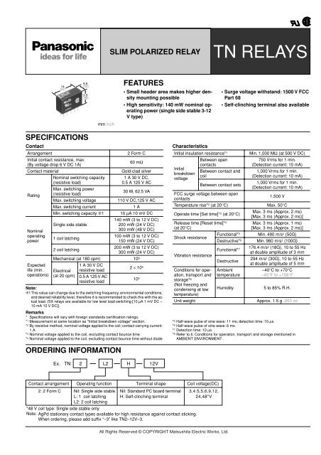
SPECIFICATIONS<br />
mm inch<br />
SLIM POLARIZED <strong>RELAY</strong><br />
FEATURES<br />
Contact<br />
Arrangement 2 Form C<br />
Initial contact resistance, max.<br />
(By voltage drop 6 V DC 1A)<br />
60 mΩ<br />
Contact material Gold-clad silver<br />
Nominal switching capacity 1 A 30 V DC,<br />
(resistive load)<br />
0.5 A 125 V AC<br />
Rating<br />
Max. switching power<br />
(resistive load)<br />
30 W, 62.5 VA<br />
Max. switching voltage 110 V DC,125 V AC<br />
Max. switching current 1 A<br />
Min. switching capacity ❇1<br />
10 µ A 10 mV DC<br />
140 mW (3 to 12 V DC)<br />
Single side stable<br />
200 mW (24 V DC)<br />
Nominal<br />
300 mW (48 V DC)<br />
operating<br />
power<br />
1 coil latching<br />
100 mW (3 to 12 V DC)<br />
150 mW (24 V DC)<br />
2 coil latching<br />
200 mW (3 to 12 V DC)<br />
300 mW (24 V DC)<br />
Mechanical (at 180 cpm) 108<br />
Expected<br />
life (min.<br />
operations)<br />
Note:<br />
Electrical<br />
(at 20 cpm)<br />
1 A 30 V DC<br />
resistive load<br />
0.5 A 125 V AC<br />
resistive load<br />
2 × 10⁵<br />
105<br />
❇1This<br />
value can change due to the switching frequency, environmental conditions,<br />
and desired reliability level, therefore it is recommended to check this with the actual<br />
load. (SX relays are available for low level load switching [10 µA 1 mV DC –<br />
10 mA 10 V DC])<br />
Remarks<br />
* Specifications will vary with foreign standards certification ratings.<br />
* 1 Measurement at same location as "Initial breakdown voltage" section.<br />
* 2 By resistive method, nominal voltage applied to the coil; contact carrying current:<br />
1 A.<br />
* 3 Nominal voltage applied to the coil, excluding contact bounce time.<br />
* 4 Nominal voltage applied to the coil, excluding contact bounce time without diode.<br />
ORDERING INFORMATION<br />
Ex. <strong>TN</strong> 2 <strong>L2</strong> H 12V<br />
• Small header area makes higher density<br />
mounting possible<br />
• High sensitivity: 140 mW nominal operating<br />
power (single side stable 3-12<br />
V type)<br />
Characteristics<br />
Initial insulation resistance* 1<br />
Initial<br />
breakdown<br />
voltage<br />
<strong>TN</strong> <strong>RELAY</strong>S<br />
Between open<br />
contacts<br />
Between contact and<br />
coil<br />
• Surge voltage withstand: 1500 V FCC<br />
Part 68<br />
• Self-clinching terminal also available<br />
Between contact sets<br />
Min. 1,000 MΩ<br />
(at 500 V DC)<br />
750 Vrms for 1 min.<br />
(Detection current: 10 mA)<br />
1,000 Vrms for 1 min.<br />
(Detection current: 10 mA)<br />
1,000 Vrms for 1 min.<br />
(Detection current: 10 mA)<br />
FCC surge voltage between open<br />
contacts<br />
1,500 V<br />
Temperature rise* 2 (at 20°<br />
C) Max. 50°<br />
C<br />
Operate time [Set time]* 3 (at 20°<br />
C)<br />
Release time [Reset time]* 4<br />
(at 20°<br />
C)<br />
Shock resistance<br />
Vibration resistance<br />
Contact arrangement Operating function Terminal shape Coil voltage(DC)<br />
2: 2 Form C Nil: Single side stable Nil: Standard PC board terminal 3,4.5,5,6,9,12,<br />
L: 1 coil latching<br />
<strong>L2</strong>: 2 coil latching<br />
H: Self-clinching terminal<br />
24,48*V<br />
*48 V coil type: Single side stable only<br />
Note: AgPd stationary contact types available for high resistance against contact sticking.<br />
When ordering, please add suffix “–3” like <strong><strong>TN</strong>2</strong>–12V–3.<br />
Functional* 5<br />
Destructive* 6<br />
Functional* 7<br />
Destructive<br />
All Rights Reserved © COPYRIGHT Matsushita Electric Works, Ltd.<br />
Max. 3 ms (Approx. 2 ms)<br />
[Max. 3 ms (Approx. 2 ms)]<br />
Max. 3 ms (Approx. 1 ms)<br />
[Max. 3 ms (Approx. 2 ms)]<br />
Min. 490 m/s2<br />
{50G}<br />
Min. 980 m/s2<br />
{100G}<br />
176.4 m/s2<br />
{18G}, 10 to 55 Hz<br />
at double amplitude of 3 mm<br />
294 m/s2<br />
{30G}, 10 to 55 Hz<br />
at double amplitude of 5 mm<br />
–40°<br />
C to +70°<br />
C<br />
–40°<br />
F to +158°<br />
F<br />
Conditions for oper- Ambient<br />
ation, transport and<br />
storage* 8<br />
temperature<br />
(Not freezing and<br />
condensing at low<br />
temperature)<br />
Humidity 5 to 85% R.H.<br />
Unit weight Approx. 1.5 g .053 oz<br />
* 5 Half-wave pulse of sine wave: 11 ms; detection time: 10 µ s.<br />
* 6 Half-wave pulse of sine wave: 6 ms.<br />
* 7 Detection time: 10 µ s.<br />
* 8 Refer to 6. Conditions for operation, transport and storage mentioned in<br />
AMBIENT ENVIRONMENT .
<strong>TN</strong><br />
TYPES AND <strong>COIL</strong> DATA (at 20°<br />
C 68°<br />
F)<br />
1. Single side stable<br />
Part No.<br />
Standard PC<br />
board terminal<br />
2. 1 Coil latching<br />
Part No.<br />
3. 2 Coil latching<br />
Part No.<br />
Self-clinching<br />
terminal<br />
Nominal<br />
voltage,<br />
V DC<br />
Pick-up<br />
voltage,<br />
V DC (max.)<br />
Drop-out<br />
voltage,<br />
V DC (min.)<br />
Nominal<br />
operating<br />
current,<br />
mA ( ± 10%)<br />
Coil<br />
resistance,<br />
Ω ( ± 10%)<br />
Notes:<br />
1. Specified value of the pick-up, drop-out, set and reset voltage is with the condition of square wave coil pulse.<br />
2. Standard packing: Tube: 50 pcs.; Case: 1,000 pcs.<br />
3. In case of 5 V drive circuit, it is recommended to use 4.5 V type relay.<br />
4. AgPd stationary contact types available for high resistance against contact sticking. When ordering, please add suffix "–3" like <strong><strong>TN</strong>2</strong>-12V-3.<br />
Nominal<br />
operating<br />
power,<br />
mW<br />
Max.<br />
allowable<br />
voltage,<br />
V DC<br />
<strong><strong>TN</strong>2</strong>-3 V <strong><strong>TN</strong>2</strong>-H-3 V 3 2.25 0.3 46.7 64.3 140 4.5<br />
<strong><strong>TN</strong>2</strong>-4.5 V <strong><strong>TN</strong>2</strong>-H-4.5 V 4.5 3.38 0.45 31.1 145 140 6.7<br />
<strong><strong>TN</strong>2</strong>-5 V <strong><strong>TN</strong>2</strong>-H-5 V 5 3.75 0.5 28.1 178 140 7.5<br />
<strong><strong>TN</strong>2</strong>-6 V <strong><strong>TN</strong>2</strong>-H-6 V 6 4.5 0.6 23.3 257 140 9<br />
<strong><strong>TN</strong>2</strong>-9 V <strong><strong>TN</strong>2</strong>-H-9 V 9 6.75 0.9 15.5 579 140 13.5<br />
<strong><strong>TN</strong>2</strong>-12 V <strong><strong>TN</strong>2</strong>-H-12 V 12 9 1.2 11.7 1,028 140 18<br />
<strong><strong>TN</strong>2</strong>-24 V <strong><strong>TN</strong>2</strong>-H-24 V 24 18 2.4 8.3 2,880 200 36<br />
<strong><strong>TN</strong>2</strong>-48 V <strong><strong>TN</strong>2</strong>-H-48 V 48 36 4.8 6.25 7,680 300 57.6<br />
Standard PC<br />
board terminal<br />
Self-clinching<br />
terminal<br />
Nominal<br />
voltage,<br />
V DC<br />
Set voltage,<br />
V DC (max.)<br />
Reset voltage,<br />
V DC (max.)<br />
Nominal<br />
operating<br />
current,<br />
mA ( ± 10%)<br />
Coil<br />
resistance,<br />
Ω ( ± 10%)<br />
Nominal<br />
operating<br />
power,<br />
mW<br />
Max.<br />
allowable<br />
voltage,<br />
V DC<br />
<strong><strong>TN</strong>2</strong>-L-3 V <strong><strong>TN</strong>2</strong>-L-H-3 V 3 2.25 2.25 33.3 90 100 4.5<br />
<strong><strong>TN</strong>2</strong>-L-4.5 V <strong><strong>TN</strong>2</strong>-L-H-4.5 V 4.5 3.38 3.38 22.2 202.5 100 6.7<br />
<strong><strong>TN</strong>2</strong>-L-5 V <strong><strong>TN</strong>2</strong>-L-H-5 V 5 3.75 3.75 20 250 100 7.5<br />
<strong><strong>TN</strong>2</strong>-L-6 V <strong><strong>TN</strong>2</strong>-L-H-6 V 6 4.5 4.5 16.7 360 100 9<br />
<strong><strong>TN</strong>2</strong>-L-9 V <strong><strong>TN</strong>2</strong>-L-H-9 V 9 6.75 6.75 11.1 810 100 13.5<br />
<strong><strong>TN</strong>2</strong>-L-12 V <strong><strong>TN</strong>2</strong>-L-H-12 V 12 9 9 8.3 1,440 100 18<br />
<strong><strong>TN</strong>2</strong>-L-24 V <strong><strong>TN</strong>2</strong>-L-H-24 V 24 18 18 6.3 3,840 150 36<br />
Standard PC<br />
board terminal<br />
Self-clinching<br />
terminal<br />
Nominal<br />
voltage,<br />
V DC<br />
Set voltage,<br />
V DC (max.)<br />
Reset voltage,<br />
V DC (max.)<br />
Nominal<br />
operating<br />
current,<br />
mA ( ± 10%)<br />
Coil<br />
resistance,<br />
Ω ( ± 10%)<br />
Nominal<br />
operating<br />
power,<br />
mW<br />
Max.<br />
allowable<br />
voltage,<br />
V DC<br />
<strong><strong>TN</strong>2</strong>-<strong>L2</strong>-3 V <strong><strong>TN</strong>2</strong>-<strong>L2</strong>-H-3 V 3 2.25 2.25 66.7 45 200 4.5<br />
<strong><strong>TN</strong>2</strong>-<strong>L2</strong>-4.5 V <strong><strong>TN</strong>2</strong>-<strong>L2</strong>-H-4.5 V 4.5 3.38 3.38 44.4 101.2 200 6.7<br />
<strong><strong>TN</strong>2</strong>-<strong>L2</strong>-5 V <strong><strong>TN</strong>2</strong>-<strong>L2</strong>-H-5 V 5 3.75 3.75 40 125 200 7.5<br />
<strong><strong>TN</strong>2</strong>-<strong>L2</strong>-6 V <strong><strong>TN</strong>2</strong>-<strong>L2</strong>-H-6 V 6 4.5 4.5 33.3 180 200 9<br />
<strong><strong>TN</strong>2</strong>-<strong>L2</strong>-9 V <strong><strong>TN</strong>2</strong>-<strong>L2</strong>-H-9 V 9 6.75 6.75 22.2 405 200 13.5<br />
<strong><strong>TN</strong>2</strong>-<strong>L2</strong>-12 V <strong><strong>TN</strong>2</strong>-<strong>L2</strong>-H-12 V 12 9 9 16.7 720 200 18<br />
<strong><strong>TN</strong>2</strong>-<strong>L2</strong>-24 V <strong><strong>TN</strong>2</strong>-<strong>L2</strong>-H-24 V 24 18 18 12.5 1,920 300 28.8<br />
DIMENSIONS<br />
9.8 9.5<br />
.386 .374<br />
3.5<br />
.138<br />
9.8 9.5<br />
.386 .374<br />
3.5<br />
.138<br />
Standard PC board terminal<br />
2.54<br />
.100<br />
2.54<br />
.100<br />
14<br />
551<br />
0.5<br />
.020<br />
Self-clinching terminal<br />
14<br />
551<br />
0.5<br />
.020<br />
5.6<br />
.220<br />
0.25<br />
1.385 .010<br />
.055 2.54<br />
.100<br />
1.385<br />
.055<br />
General tolerance: ± 0.3 ± .012<br />
5.6<br />
.220<br />
0.25<br />
.010<br />
2.54<br />
.100<br />
• Single side stable<br />
(Deenergized condition)<br />
1 2 3 4 5<br />
10 9 8 7 6<br />
Direction indication*<br />
PC board pattern (Copper-side view)<br />
10.16<br />
.400<br />
2.54<br />
.100<br />
10-1.0 dia. hole<br />
10-.039 dia. hole<br />
2.54<br />
.100<br />
Schematic (Bottom view)<br />
• 1-coil latching<br />
(Reset condition)<br />
10 9 8 7 6<br />
Direction indication*<br />
All Rights Reserved © COPYRIGHT Matsushita Electric Works, Ltd.<br />
1 2 3 4 5<br />
mm inch<br />
Tolerance: ± 0.1 ± .004<br />
• 2-coil latching<br />
(Reset condition)<br />
1 2 3 4 5<br />
10 9 8 7 6<br />
Direction indication*<br />
*Orientation stripe located on top of relay
REFERENCE DATA<br />
1. Maximum switching capacity 2. Life curve 3. Mechanical life<br />
Tested sample: <strong><strong>TN</strong>2</strong>-12V, 10 pcs.<br />
Switching current, A<br />
1.0<br />
0.5<br />
0.4<br />
0.3<br />
0.2<br />
DC load (cosϕ=1)<br />
AC load (cosϕ=1)<br />
30 100<br />
Switching voltage,V<br />
200<br />
4. Electrical life (DC load)<br />
Tested sample: <strong><strong>TN</strong>2</strong>-12V, 10 pcs.<br />
Condition: 1 A 30 V DC resistive load, 20 cpm<br />
No. of operations, ×10 4<br />
100<br />
10<br />
30 V DC resistive load<br />
125 V AC resistive load<br />
0 0.5 1.0<br />
Switching current, A<br />
Change of pick-up and drop-out voltage Change of contact resistance<br />
Ratio against the rated voltage %V<br />
100<br />
90<br />
80<br />
70<br />
60<br />
50<br />
40<br />
30<br />
20<br />
10<br />
0<br />
Pick-up voltage<br />
Drop-out voltage<br />
No. of operations, ×10 4<br />
5 10 15 20<br />
6. Operate/release time characteristics<br />
Tested sample: <strong><strong>TN</strong>2</strong>-12V, 5 pcs.<br />
Operate and release time, ms<br />
6<br />
5<br />
4<br />
3<br />
2<br />
1<br />
0<br />
Operate time<br />
Release time<br />
80 90 100 110 120<br />
Coil applied voltage, %V<br />
9. Distribution of set and reset voltage<br />
Tested sample: <strong><strong>TN</strong>2</strong>-<strong>L2</strong>-12V, 32 pcs.<br />
Quantity<br />
;;;<br />
;;;<br />
;;<br />
;;<br />
30<br />
20<br />
;;;<br />
;;<br />
;;<br />
10<br />
;<br />
Max.<br />
Min.<br />
Max.<br />
Min.<br />
Set voltage<br />
Reset voltage<br />
0 10 20 30 40 50 60 70 80 90 100<br />
Ratio against the rated voltage, %V<br />
Max.<br />
Min.<br />
Max.<br />
Min.<br />
Contact resistance,mΩ<br />
100<br />
90<br />
80<br />
70<br />
60<br />
50<br />
40<br />
30<br />
20<br />
10<br />
0<br />
Terminal No.2–3–4<br />
Terminal No.7–8–9<br />
5 10 15 20<br />
No.of operations, ×10 4<br />
7. Set/reset time characteristics<br />
Tested sample: <strong><strong>TN</strong>2</strong>-<strong>L2</strong>-12V, 5 pcs.<br />
Set and reset time, ms<br />
6<br />
5<br />
4<br />
3<br />
2<br />
1<br />
0<br />
Set time<br />
Reset time<br />
80 90 100 110 120<br />
Coil applied voltage, %V<br />
Max.<br />
Min.<br />
10. Ambient temperature characteristics<br />
Tested sample: <strong><strong>TN</strong>2</strong>-12V, 5 pcs.<br />
Variation<br />
ratio, %<br />
40<br />
30<br />
20<br />
Drop-out<br />
voltage<br />
–40 –20 –10<br />
10<br />
0 Pick-up voltage<br />
Ambient<br />
temperature, °C<br />
20 40<br />
–10<br />
60 80<br />
All Rights Reserved © COPYRIGHT Matsushita Electric Works, Ltd.<br />
–20<br />
–30<br />
–40<br />
x<br />
x<br />
Ratio against the rated voltage, %V<br />
100<br />
90<br />
80<br />
70<br />
60<br />
50<br />
40<br />
30<br />
20<br />
10<br />
0<br />
Pick-up voltage<br />
Drop-out voltage<br />
<strong>TN</strong><br />
Max.<br />
Min.<br />
Max.<br />
Min.<br />
10 100 1,000 10,000<br />
No. of operations, ×10 4<br />
5. Coil temperature rise<br />
Tested sample: <strong><strong>TN</strong>2</strong>-12V<br />
Point measured: Inside the coil<br />
Ambient temperature: Room temperature (25°<br />
to<br />
26°<br />
C), 70°<br />
C (77°<br />
to 79°<br />
F), 158°<br />
F<br />
Temperature rise, °C<br />
70<br />
60<br />
50<br />
40<br />
30<br />
20<br />
10<br />
0<br />
Carrying current<br />
0 A (Room temp.)<br />
1 A (Room temp.)<br />
0 A (70°C)<br />
1 A (70°C)<br />
80 90 100 110 120 130 140 150<br />
Coil applied voltage, %V<br />
8. Distribution of pick-up and drop-out voltages<br />
Tested sample: <strong><strong>TN</strong>2</strong>-12V, 40 pcs.<br />
Quantity<br />
30<br />
20<br />
10<br />
Drop-out voltage<br />
Pick-up voltage<br />
0 10 20 30 40 50 60 70 80 90 100<br />
Ratio against the rated voltage, %V<br />
11. Distribution of contact resistance<br />
Tested sample: <strong><strong>TN</strong>2</strong>-12V, 38 pcs. (38×<br />
4 contacts)<br />
Quantity<br />
40<br />
30<br />
20<br />
10<br />
Terminal<br />
No.<br />
7,8,9<br />
Side<br />
Terminal No.<br />
2,3,4 side<br />
0 30 40 50<br />
Contact resistance,mΩ<br />
1 2 3 4 5<br />
6 7 8 9 10
<strong>TN</strong><br />
12-(1). Malfunctional shock (single side stable)<br />
Tested sample: <strong><strong>TN</strong>2</strong>-12V, 6 pcs.<br />
X<br />
X ,<br />
X<br />
Z Z ,<br />
980m/s 2<br />
Y Y ,<br />
980m/s 2<br />
Y<br />
Z ,<br />
X ,<br />
980m/s 2 980m/s 2<br />
980m/s 2<br />
Y ,<br />
Deenergized condition<br />
Energized condition<br />
Z<br />
980m/s 2<br />
12-(2). Malfunctional shock (latching)<br />
Tested sample: <strong><strong>TN</strong>2</strong>-<strong>L2</strong>-12V, 6 pcs.<br />
X ,<br />
X<br />
Z Z ,<br />
X<br />
980m/s 2<br />
Z ,<br />
980m/s 2<br />
Y Y ,<br />
980m/s 2<br />
Y<br />
980m/s 2<br />
Y ,<br />
Deenergized condition<br />
Energized condition<br />
13-(1). Influence of adjacent mounting 13-(2). Influence of adjacent mounting<br />
Rate of change, % Rate of change, %<br />
10<br />
0<br />
–10<br />
10<br />
0<br />
–10<br />
Pick-up voltage<br />
Drop-out voltage<br />
ON<br />
OFF<br />
ON<br />
OFF<br />
ON<br />
OFF<br />
0 5<br />
.197<br />
Inter-relay distance , mm inch<br />
14. Actual load test<br />
(35 mA 48 V DC wire spring relay load)<br />
Circuit<br />
48 V<br />
DC<br />
0.1<br />
µF<br />
0.1<br />
µF<br />
500Ω<br />
3<br />
2<br />
500Ω<br />
Wire spring relay Circuit diagram<br />
15-(1). High-frequency characteristics<br />
Tested sample: <strong><strong>TN</strong>2</strong>-xxV<br />
Isolation characteristics<br />
Isolation, dB<br />
100<br />
50<br />
Terminal No. 7–8–9<br />
Terminal No. 2–3–4<br />
10 100 1000<br />
Frequency, MHz<br />
Rate of change, % Rate of change, %<br />
Ratio against the rated voltage, %V<br />
10<br />
0<br />
–10<br />
20<br />
10<br />
0<br />
Pick-up voltage<br />
Drop-out voltage<br />
ON<br />
OFF<br />
Z<br />
980m/s 2<br />
X ,<br />
980m/s 2<br />
ON<br />
OFF<br />
ON<br />
OFF<br />
0 5<br />
.197<br />
Inter-relay distance , mm inch<br />
Change of pick-up and drop-out voltage Change of contact resistance<br />
100<br />
100<br />
90<br />
90<br />
80<br />
80<br />
70<br />
Pick-up voltage<br />
Max.<br />
70<br />
60<br />
Min.<br />
60<br />
50<br />
50<br />
40<br />
40<br />
Terminal No. 2–3<br />
Drop-out voltage<br />
30<br />
Max.<br />
30<br />
20<br />
Min.<br />
20<br />
10<br />
10<br />
0 10<br />
No. of operations,×10 4<br />
20 30 40 50<br />
15-(2). High-frequency characteristics<br />
Tested sample: <strong><strong>TN</strong>2</strong>-xxV<br />
Insertion loss characteristics<br />
Insertion loss, dB<br />
1.6<br />
1.4<br />
1.2<br />
1.0<br />
0.8<br />
0.6<br />
0.4<br />
0.2<br />
Terminal No. 2–3–4<br />
Terminal No. 7–8–9<br />
10 100 1000<br />
Frequency, MHz<br />
For Cautions for Use, see Relay Technical Information.<br />
Contact resistance, mΩ<br />
0 10<br />
All Rights Reserved © COPYRIGHT Matsushita Electric Works, Ltd.<br />
No. of operations, ×10 4<br />
20 30 40 50<br />
15-(3). High-frequency characteristics<br />
Tested sample: <strong><strong>TN</strong>2</strong>-xxV<br />
V.S.W.R.<br />
V.S.W.R.<br />
2.2<br />
2.1<br />
2.0<br />
1.9<br />
1.8<br />
1.7<br />
1.6<br />
1.5<br />
1.4<br />
1.3<br />
1.2<br />
1.1<br />
1.0<br />
Terminal No. 2-3-4<br />
Terminal No. 7-8-9<br />
Max.<br />
Min.<br />
10 100 1000<br />
Frequency, MHz