DM74LS151 1-of-8 Line Data Selector/Multiplexer
DM74LS151 1-of-8 Line Data Selector/Multiplexer
DM74LS151 1-of-8 Line Data Selector/Multiplexer

Create successful ePaper yourself
Turn your PDF publications into a flip-book with our unique Google optimized e-Paper software.
<strong>DM74LS151</strong><br />
1-<strong>of</strong>-8 <strong>Line</strong> <strong>Data</strong> <strong>Selector</strong>/<strong>Multiplexer</strong><br />
General Description<br />
This data selector/multiplexer contains full on-chip decoding<br />
to select the desired data source. The <strong>DM74LS151</strong><br />
selects one-<strong>of</strong>-eight data sources. The <strong>DM74LS151</strong> has a<br />
strobe input which must be at a low logic level to enable<br />
these devices. A high level at the strobe forces the W output<br />
HIGH, and the Y output LOW.<br />
The <strong>DM74LS151</strong> features complementary W and Y outputs.<br />
Ordering Code:<br />
Features<br />
Devices also available in Tape and Reel. Specify by appending the suffix letter “X” to the ordering code.<br />
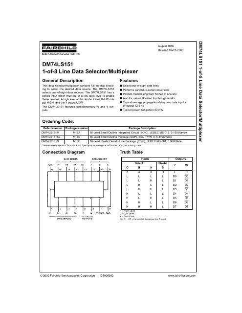
Connection Diagram Truth Table<br />
August 1986<br />
Revised March 2000<br />
■ Select one-<strong>of</strong>-eight data lines<br />
■ Performs parallel-to-serial conversion<br />
■ Permits multiplexing from N lines to one line<br />
■ Also for use as Boolean function generator<br />
■ Typical average propagation delay time data input to<br />
W output 12.5 ns<br />
■ Typical power dissipation 30 mW<br />
Order Number Package Number Package Description<br />
<strong>DM74LS151</strong>M M16A 16-Lead Small Outline Integrated Circuit (SOIC), JEDEC MS-012, 0.150 Narrow<br />
<strong>DM74LS151</strong>SJ M16D 16-Lead Small Outline Package (SOP), EIAJ TYPE II, 5.3mm Wide<br />
<strong>DM74LS151</strong>N N16E 16-Lead Plastic Dual-In-<strong>Line</strong> Package (PDIP), JEDEC MS-001, 0.300 Wide<br />
Inputs Outputs<br />
C<br />
Select<br />
B A<br />
Strobe<br />
S<br />
Y W<br />
X X X H L H<br />
L L L L D0 D0<br />
L L H L D1 D1<br />
L H L L D2 D2<br />
L H H L D3 D3<br />
H L L L D4 D4<br />
H L H L D5 D5<br />
H H L L D6 D6<br />
H H H L D7 D7<br />
H = HIGH Level<br />
L = LOW Level<br />
X = Don't Care<br />
D0, D1...D7 = the level <strong>of</strong> the respective D input<br />
© 2000 Fairchild Semiconductor Corporation DS006392 www.fairchildsemi.com<br />
<strong>DM74LS151</strong> 1-<strong>of</strong>-8 <strong>Line</strong> <strong>Data</strong> <strong>Selector</strong>/<strong>Multiplexer</strong>
<strong>DM74LS151</strong><br />
Logic Diagrams<br />
See Address Buffers<br />
Address Buffers<br />
www.fairchildsemi.com 2
Absolute Maximum Ratings(Note 1)<br />
Supply Voltage 7V<br />
Input Voltage 7V<br />
Operating Free Air Temperature Range 0°C to +70°C<br />
Storage Temperature Range −65°C to +150°C<br />
Recommended Operating Conditions<br />
Electrical Characteristics<br />
Note 2: All typicals are at VCC = 5V, TA = 25°C.<br />
Note 3: Not more than one output should be shorted at a time, and the duration should not exceed one second.<br />
Note 4: ICC is measured with all outputs OPEN, strobe and data select inputs at 4.5V, and all other inputs OPEN.<br />
Note 1: The “Absolute Maximum Ratings” are those values beyond which<br />
the safety <strong>of</strong> the device cannot be guaranteed. The device should not be<br />
operated at these limits. The parametric values defined in the Electrical<br />
Characteristics tables are not guaranteed at the absolute maximum ratings.<br />
The “Recommended Operating Conditions” table will define the conditions<br />
for actual device operation.<br />
Symbol Parameter Min Nom Max Units<br />
VCC Supply Voltage 4.75 5 5.25 V<br />
VIH HIGH Level Input Voltage 2 V<br />
VIL LOW Level Input Voltage 0.8 V<br />
IOH HIGH Level Output Current −0.4 mA<br />
IOL LOW Level Output Current 8 mA<br />
TA Free Air Operating Temperature 0 70 °C<br />
over recommended operating free air temperature range (unless otherwise noted)<br />
Typ<br />
Symbol Parameter Conditions Min<br />
(Note 2)<br />
Max Units<br />
VI Input Clamp Voltage VCC = Min, II = −18 mA −1.5 V<br />
VOH HIGH Level<br />
Output Voltage<br />
VCC = Min, IOH = Max<br />
VIL = Max, VIH = Min<br />
2.7 3.4 V<br />
VOL LOW Level<br />
Output Voltage<br />
VCC = Min, IOL = Max<br />
VIL = Max, VIH = Min<br />
0.35 0.5<br />
V<br />
IOL = 4 mA, VCC = Min 0.25 0.4<br />
II Input Current @ Max Input Voltage VCC = Max, VI = 7V 0.1 mA<br />
IIH HIGH Level Input Current VCC = Max, VI = 2.7V 20 μA<br />
IIL LOW Level Input Current VCC = Max, VI = 0.4V −0.4 mA<br />
IOS Short Circuit Output Current VCC = Max (Note 3) −20 −100 mA<br />
ICC Supply Current VCC = Max (Note 4) 6 10 mA<br />
3 www.fairchildsemi.com<br />
<strong>DM74LS151</strong>
<strong>DM74LS151</strong><br />
Switching Characteristics<br />
at VCC = 5V and TA = 25°C<br />
From (Input) RL = 2 kΩ<br />
Symbol Parameter To (output) CL = 15 pF CL = 50 pF Units<br />
Min Max Min Max<br />
tPLH Propagation Delay Time<br />
LOW-to-HIGH Level Output<br />
Select<br />
(4 Levels) to Y<br />
43 46 ns<br />
tPHL Propagation Delay Time<br />
HIGH-to-LOW Level Output<br />
Select<br />
(4 Levels) to Y<br />
30 36 ns<br />
tPLH Propagation Delay Time<br />
LOW-to-HIGH Level Output<br />
Select<br />
(3 Levels) to W<br />
23 25 ns<br />
tPHL Propagation Delay Time<br />
HIGH-to-LOW Level Output<br />
Select<br />
(3 Levels) to W<br />
32 40 ns<br />
tPLH Propagation Delay Time<br />
LOW-to-HIGH Level Output<br />
Strobe<br />
to Y<br />
42 44 ns<br />
tPHL Propagation Delay Time<br />
HIGH-to-LOW Level Output<br />
Strobe<br />
to Y<br />
32 40 ns<br />
tPLH Propagation Delay Time<br />
LOW-to-HIGH Level Output<br />
Strobe<br />
to W<br />
24 27 ns<br />
tPHL Propagation Delay Time<br />
HIGH-to-LOW Level Output<br />
Strobe<br />
to W<br />
30 36 ns<br />
tPLH Propagation Delay Time<br />
LOW-to-HIGH Level Output<br />
D0 thru D7<br />
to Y<br />
32 35 ns<br />
tPHL Propagation Delay Time<br />
HIGH-to-LOW Level Output<br />
D0 thru D7<br />
to Y<br />
26 33 ns<br />
tPLH Propagation Delay Time<br />
LOW-to-HIGH Level Output<br />
D0 thru D7<br />
to W<br />
21 25 ns<br />
tPHL Propagation Delay Time<br />
HIGH-to-LOW Level Output<br />
D0 thru D7<br />
to W<br />
20 27 ns<br />
www.fairchildsemi.com 4
Physical Dimensions inches (millimeters) unless otherwise noted<br />
16-Lead Small Outline Integrated Circuit (SOIC), JEDEC MS-012, 0.150 Narrow<br />
Package Number M16A<br />
5 www.fairchildsemi.com<br />
<strong>DM74LS151</strong>
<strong>DM74LS151</strong><br />
Physical Dimensions inches (millimeters) unless otherwise noted (Continued)<br />
16-Lead Small Outline Package (SOP), EIAJ TYPE II, 5.3mm Wide<br />
Package Number M16D<br />
www.fairchildsemi.com 6
Physical Dimensions inches (millimeters) unless otherwise noted (Continued)<br />
16-Lead Plastic Dual-In-<strong>Line</strong> Package (PDIP), JEDEC MS-001, 0.300 Wide<br />
Package Number N16E<br />
Fairchild does not assume any responsibility for use <strong>of</strong> any circuitry described, no circuit patent licenses are implied and<br />
Fairchild reserves the right at any time without notice to change said circuitry and specifications.<br />
LIFE SUPPORT POLICY<br />
FAIRCHILD’S PRODUCTS ARE NOT AUTHORIZED FOR USE AS CRITICAL COMPONENTS IN LIFE SUPPORT<br />
DEVICES OR SYSTEMS WITHOUT THE EXPRESS WRITTEN APPROVAL OF THE PRESIDENT OF FAIRCHILD<br />
SEMICONDUCTOR CORPORATION. As used herein:<br />
1. Life support devices or systems are devices or systems<br />
which, (a) are intended for surgical implant into the<br />
body, or (b) support or sustain life, and (c) whose failure<br />
to perform when properly used in accordance with<br />
instructions for use provided in the labeling, can be reasonably<br />
expected to result in a significant injury to the<br />
user.<br />
2. A critical component in any component <strong>of</strong> a life support<br />
device or system whose failure to perform can be reasonably<br />
expected to cause the failure <strong>of</strong> the life support<br />
device or system, or to affect its safety or effectiveness.<br />
www.fairchildsemi.com<br />
7 www.fairchildsemi.com<br />
<strong>DM74LS151</strong> 1-<strong>of</strong>-8 <strong>Line</strong> <strong>Data</strong> <strong>Selector</strong>/<strong>Multiplexer</strong>