
You also want an ePaper? Increase the reach of your titles
YUMPU automatically turns print PDFs into web optimized ePapers that Google loves.
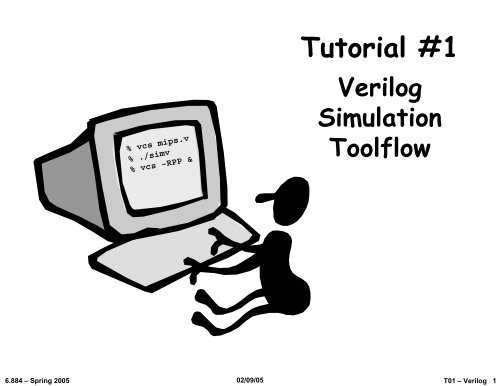
% vcs mips.v<br />
% ./simv<br />
% vcs –RPP &<br />
6.884 – Spring 2005 02/09/05<br />
<strong>Tutorial</strong> <strong>#1</strong><br />
Verilog<br />
Simulation<br />
Toolflow<br />
T01 – Verilog 1
StdCell<br />
Library<br />
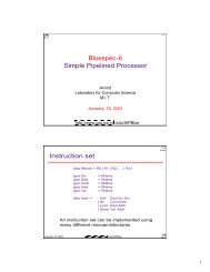
6.884 Toolflow For Lab 1 and 2<br />
StdCell<br />
Library<br />
Synopsys DC<br />
Verilog<br />
Gate<br />
Level<br />
Cadence Encounter<br />
Timing<br />
Area<br />
Power<br />
Verilog<br />
Source<br />
Synopsys VirSim<br />
6.884 – Spring 2005 02/09/05<br />
Synopsys VCS<br />
Func<br />
Sim<br />
Test Scripts<br />
Test<br />
Outputs<br />
Assembly<br />
Source<br />
Code<br />
SMIPS Assembler<br />
Test<br />
Inputs<br />
T01 – Verilog 2
Tour of the 6.884 Athena Locker<br />
To access the locker use setup 6.884<br />
– /mit/6.884/tools<br />
– /mit/6.884/doc<br />
– /mit/6.884/examples<br />
For those with access to the CAG network please<br />
make use of the CAG infrastructure<br />
–Use setup 6.884 (will setup tools needed for the course)<br />
– Locker (partially) mirrored at /projects/assam/6.884<br />
– CAG updates will probably lag a bit behind Athena<br />
6.884 – Spring 2005 02/09/05<br />
T01 – Verilog 3
GCD<br />
Three Examples<br />
Beta<br />
6.884 – Spring 2005 02/09/05<br />
Lab1<br />
T01 – Verilog 4
A_in<br />
B_in<br />
Greatest Common Divisor<br />
Control Unit<br />
go A A<br />
mux reg<br />
B<br />
mux<br />
B<br />
reg<br />
out<br />
mux<br />
done<br />
sel en sel en B = 0<br />
A < B<br />
sel<br />
6.884 – Spring 2005 02/09/05<br />
A<br />
B<br />
zero? lt<br />
sub<br />
out<br />
T01 – Verilog 5
while ( !done )<br />
if ( A < B )<br />
swap( A, B )<br />
else if ( B != 0 )<br />
A = A – B<br />
else<br />
done = true<br />
endwhile<br />
GCD Control Logic<br />
Load<br />
Swap<br />
Sub<br />
Done<br />
reg [5:0] ctrl_sig;<br />
assign { A_en, B_en, A_mux_sel, B_mux_sel, out_mux_sel, done } = ctrl_sig;<br />
always @(*)<br />
begin<br />
if ( !running ) ctrl_sig = 6'b11_00x_0; // Latch in A and B values<br />
else if ( A_lt_B ) ctrl_sig = 6'b11_111_0; // A
A_in<br />
B_in<br />
GCD Test Harness<br />
6.884 – Spring 2005 02/09/05<br />
A<br />
B<br />
Control Unit<br />
go A A B B<br />
out done<br />
mux<br />
sel<br />
reg<br />
en<br />
mux<br />
sel<br />
reg<br />
en<br />
B = 0<br />
A < B<br />
zero? lt<br />
sub<br />
mux<br />
sel<br />
out<br />
T01 – Verilog 7
module gcd_test;<br />
reg clock = 0; reg reset = 0; reg go = 0;<br />
reg [15:0] A_in, B_in;<br />
wire done;<br />
wire [15:0] Y;<br />
always <strong>#1</strong>0 clock = ~clock;<br />
gcd_rtl gcd_unit( .clock(clock), .reset(reset), .go(go),<br />
.A_in(A_in), .B_in(B_in), .done(done), .Y(Y) );<br />
initial begin<br />
$vcdpluson(0);<br />
A_in = 27; B_in = 15; // Set defaults<br />
$value$plusargs("a-in=%d",A_in); // Read in cmdline args<br />
$value$plusargs("b-in=%d",B_in);<br />
#5 reset = 1; #20 reset = 0; // Strobe reset signal<br />
#20 go = 1; #20 go = 0; // Strobe go signal<br />
end<br />
always @( done ) begin<br />
if ( done ) begin<br />
<strong>#1</strong>5;<br />
$display(" a-in = %d", A_in );<br />
$display(" b-in = %d", B_in );<br />
$display(" gcd-out = %d", Y );<br />
$finish;<br />
end<br />
end<br />
endmodule<br />
6.884 – Spring 2005 02/09/05<br />
GCD Test<br />
Harness<br />
Try to keep the Verilog<br />
part of the test harness<br />
as simple as possible!<br />
T01 – Verilog 8
Building a GCD Simulator with VCS<br />
% setup 6.884<br />
Attaching 6.884 …<br />
Running commands in /mit/6.884/.attachrc …<br />
% vcs –PP +lint=all +v2k gcd_rtl.v<br />
% ./simv<br />
VCD+ Writer 4.4R10 Copyright 1993-2004 Synopsys Inc.<br />
a-in = 27<br />
b-in = 15<br />
gcd-out = 3<br />
$finish at simulation time 245<br />
% ./simv +a-in=49 +b-in=28<br />
VCD+ Writer 4.4R10 Copyright 1993-2004 Synopsys Inc.<br />
a-in = 49<br />
b-in = 28<br />
gcd-out = 7<br />
$finish at simulation time 225<br />
% vcs –RPP &<br />
6.884 – Spring 2005 02/09/05<br />
T01 – Verilog 9
Viewing Waveforms with VirSim<br />
Browse<br />
the<br />
module<br />
hierarchy<br />
6.884 – Spring 2005 02/09/05<br />
Open up a<br />
waveform<br />
viewer<br />
Select<br />
signals<br />
for<br />
display<br />
T01 – Verilog 10
Viewing Waveforms with VirSim<br />
6.884 – Spring 2005 02/09/05<br />
T01 – Verilog 11
Using Test Scripts<br />
% vcs –PP +lint=all +v2k gcd_rtl.v<br />
% vmodel-tester.pl –v ./simv gcd-test.dat<br />
* Verilog model = ./simv<br />
* Test data file = gcd-test.dat<br />
* Running tests<br />
+ Testing a-in=27 b-in=15 gcd-out=3<br />
+ Testing a-in=21 b-in=49 gcd-out=7<br />
+ Testing a-in=25 b-in=30 gcd-out=5<br />
+ Testing a-in=19 b-in=27 gcd-out=1<br />
+ Testing a-in=40 b-in=40 gcd-out=40<br />
+ Testing a-in=250 b-in=190 gcd-out=10<br />
+ Testing a-in=5 b-in=250 gcd-out=5<br />
+ Testing a-in=0 b-in=0 gcd-out=0<br />
*** PASSED ***<br />
6.884 – Spring 2005 02/09/05<br />
T01 – Verilog 12
Using the mkasic.pl Script<br />
gcd/<br />
mkasic.pl<br />
verilog/<br />
gcd_behavioral.v<br />
gcd_rtl.v<br />
config/<br />
gcd_behavioral.cfg<br />
gcd_rtl.cfg<br />
tests/<br />
gcd-test.dat<br />
6.884 – Spring 2005 02/09/05<br />
gcd/<br />
gcd_behavioral/<br />
vcs/<br />
vcstest/<br />
gcd_rtl/<br />
vcs/<br />
vcstest/<br />
% cp –r /mit/6.884/examples/gcd<br />
% cd gcd<br />
% ./mkasic.pl –v config/gcd_rtl.cfg vcs<br />
% ./mkasic.pl –v config/gcd_behavioral.cfg vcs<br />
% ./mkasic.pl –v config/gcd_rtl.cfg vcstest<br />
% ./mkasic.pl –v config/gcd_behavioral.cfg vcstest<br />
T01 – Verilog 13
Writing Config Files for mkasic.pl<br />
#-------------------------------------------------------------------------<br />
# General configuration options<br />
package general;<br />
$outputDir = "gcd_rtl"; # Dir for all generated product<br />
$verilogSrcDir = "verilog"; # Dir where all verilog source is located<br />
$toplevelSource = "gcd_rtl.v"; # Verilog src file w/ toplevel module<br />
$toplevelModule = "gcd_test"; # Name of toplevel verlog module<br />
#-------------------------------------------------------------------------<br />
# VCS - Synopsys Verilog compiler<br />
package vcs;<br />
$simName = "gcd-rtl"; # Name to use for the VCS simulator<br />
$cmdLineOptions = ""; # Any additional VCS compiler options<br />
#-------------------------------------------------------------------------<br />
# Test<br />
package vcstest;<br />
$inputDir = "tests"; # Dir containing test inputs<br />
@testList = ( "gcd-test.dat" ); # A list of test inputs<br />
$cmdLine = "vmodel-tester.pl -v __SIMNAME__ __TESTINPUT__";<br />
return 1; # Return true for mkasic.pl<br />
6.884 – Spring 2005 02/09/05<br />
T01 – Verilog 14
PC<br />
PCSEL<br />
2<br />
XAdr<br />
4<br />
ILL<br />
OP<br />
3<br />
Beta Micro-Architecture<br />
JT<br />
2<br />
PC<br />
+4<br />
1<br />
0<br />
00<br />
PC+4+4*SXT(C)<br />
IRQ Z<br />
Instruction<br />
Memory<br />
Rc: 0<br />
WA WA<br />
ASEL 1 0<br />
6.884 – Spring 2005 02/09/05<br />
+<br />
1<br />
A<br />
D<br />
Control Logic<br />
PCSEL<br />
RA2SEL<br />
ASEL<br />
BSEL<br />
WDSEL<br />
ALUFN<br />
Wr<br />
WERF<br />
WASEL<br />
Main Datapath<br />
XP<br />
Ra: <br />
1<br />
Z<br />
C: SXT()<br />
ALUFN<br />
2<br />
WASEL<br />
Rb: <br />
Register<br />
File<br />
RA1 RA2<br />
RD1 RD2<br />
JT<br />
A B<br />
ALU<br />
PC+4<br />
0 1 2<br />
Step 1: identify memories<br />
Step 2: identify datapaths<br />
What’s left is random logic …<br />
1<br />
0 1<br />
0<br />
WDSEL<br />
Rc: <br />
RA2SEL<br />
WD<br />
WE<br />
BSEL<br />
WD<br />
Data Memory<br />
Adr<br />
1<br />
WERF<br />
RD<br />
R/W<br />
1<br />
Wr<br />
T01 – Verilog 15
module pc<br />
(<br />
input clk,<br />
input reset, // forces PC to 0x80000000<br />
input [2:0] pcsel, // selects source of next PC<br />
input [15:0] offset, // inst[15:0]<br />
input [31:0] jump_addr, // from Reg[RA], used in JMP instruction<br />
output [31:0] branch_addr, // send to datapath for LDR instruction<br />
output [31:0] pc, // used as address for instruction fetch<br />
output [31:0] pc_plus_4 // saved in regfile during branches, JMP, traps<br />
);<br />
reg [31:0] pc;<br />
wire [30:0] pcinc;<br />
wire [31:0] npc;<br />
assign pcinc = pc + 4;<br />
assign pc_plus_4 = {pc[31],pcinc};<br />
// Branch address = PC + 4 + 4*sxt(offset)<br />
assign branch_addr = {1'b0, pcinc + {{13{offset[15]}},offset[15:0],2'b00}};<br />
assign npc = reset ? 32'h80000000 :<br />
(pcsel == 0) ? {pc[31],pcinc} : // normal<br />
(pcsel == 1) ? {pc[31],branch_addr[30:0]} : // branch<br />
(pcsel == 2) ? {pc[31] & jump_addr[31],jump_addr[30:0]} : // jump<br />
(pcsel == 3) ? 32'h80000004 :<br />
(pcsel == 4) ? 32'h80000008 : // illop, trap<br />
32'hXXXXXXXX; // catch errors...<br />
always @( posedge clk )<br />
pc
module regfile<br />
(<br />
input [4:0] ra1, // address for read port 1 (Reg[RA])<br />
output [31:0] rd1, // read data for port 1<br />
input [4:0] ra2, // address for read port 2 (Reg[RB], Reg[RC] for ST)<br />
output [31:0] rd2, // read data for port 2<br />
input clk,<br />
input werf, // write enable, active high<br />
input [4:0] wa, // address for write port (Reg[RC])<br />
input [31:0] wd // write data<br />
);<br />
// The register file itself<br />
reg [31:0] registers[31:0];<br />
// read paths are combinational, register 31 is always zero register<br />
assign rd1 = (ra1 == 5'b11111) ? 32'h00000000 : registers[ra1];<br />
assign rd2 = (ra2 == 5'b11111) ? 32'h00000000 : registers[ra2];<br />
// write port is active only when WERF is asserted<br />
always @(posedge clk)<br />
begin<br />
if ( werf )<br />
registers[wa]
module datapath<br />
(<br />
input [15:0] inst, // constant field from instruction<br />
input [31:0] rd1, // Reg[RA] from register file<br />
input [31:0] rd2, // Reg[RB] from register file (Reg[RC] for ST)<br />
input [31:0] pc_plus_4, // incremented PC<br />
input [31:0] branch_addr, // PC + 4 + 4*sxt(inst[15:0])<br />
input [31:0] mem_rd_data, // memory read data (for LD)<br />
input asel, // select A operand for ALU<br />
input bsel, // select B operand for ALU<br />
input [1:0] wdsel, // select regfile write data<br />
input [5:0] alufn, // operation to be performed by alu<br />
output [31:0] wdata, // regfile write data (output of WDSEL mux)<br />
output [31:0] mem_addr, // alu output, doubles as data memory address<br />
output [31:0] jump_addr, // jump address (from Reg[RA])<br />
output [31:0] mem_wr_data, // data memory write data (from Reg[RC])<br />
output z // true if Reg[RA] is zero, used during branches<br />
);<br />
wire [31:0] alu_a; // A input to ALU<br />
wire [31:0] alu_b; // B input to ALU<br />
// compute A and B inputs into alu, also Z bit for control logic<br />
dp_misc misc(asel,bsel,inst,rd1,rd2,branch_addr,<br />
alu_a,alu_b,jump_addr,mem_wr_data,z);<br />
// where all the heavy-lifting happens<br />
dp_alu alu(alufn,alu_a,alu_b,mem_addr);<br />
// Mux to select regfile write data from PC+4, alu output, and memory data<br />
dp_wdata_mux wdata_mux(wdsel,pc_plus_4,mem_addr,mem_rd_data,wdata);<br />
endmodule<br />
6.884 – Spring 2005 02/09/05<br />
T01 – Verilog 18
PC<br />
PCSEL<br />
2<br />
XAdr<br />
4<br />
ILL<br />
OP<br />
3<br />
JT<br />
2<br />
PC<br />
+4<br />
1<br />
0<br />
00<br />
Beta Control Signals<br />
PC+4+4*SXT(C)<br />
IRQ Z<br />
Instruction<br />
Memory<br />
Rc: 0<br />
WA WA<br />
ASEL 1 0<br />
6.884 – Spring 2005 02/09/05<br />
+<br />
1<br />
A<br />
D<br />
Control Logic<br />
PCSEL<br />
RA2SEL<br />
ASEL<br />
BSEL<br />
WDSEL<br />
ALUFN<br />
Wr<br />
WERF<br />
WASEL<br />
Main Datapath<br />
XP<br />
Ra: <br />
1<br />
Z<br />
C: SXT()<br />
ALUFN<br />
2<br />
WASEL<br />
Rb: <br />
Register<br />
File<br />
RA1 RA2<br />
RD1 RD2<br />
JT<br />
A B<br />
ALU<br />
PC+4<br />
0 1 2<br />
Step 1: identify memories<br />
Step 2: identify datapaths<br />
What’s left is random logic …<br />
1<br />
0 1<br />
0<br />
WDSEL<br />
Rc: <br />
RA2SEL<br />
WD<br />
WE<br />
BSEL<br />
WD<br />
Data Memory<br />
Adr<br />
1<br />
WERF<br />
RD<br />
R/W<br />
1<br />
Wr<br />
T01 – Verilog 19
Beta Control Signals<br />
6.884 – Spring 2005 02/09/05<br />
T01 – Verilog 20
module control( ... );<br />
// Control ROM<br />
reg [15:0] ctl;<br />
always @(*)<br />
begin<br />
end<br />
if (interrupt)<br />
ctl = 16'bx_100_1xx_xxxxxx_00_0;<br />
else<br />
case (inst[31:26])<br />
// Label control signal vector here ...<br />
default: ctl = 16'bx_011_1xx_xxxxxx_00_0; // illegal opcode<br />
6'b011000: ctl = 16'bx_000_001_00xxx0_10_0; // LD<br />
6'b011001: ctl = 16'bx_000_x01_00xxx0_10_1; // ST<br />
6'b011011: ctl = 16'bx_010_0xx_xxxxxx_00_0; // JMP<br />
6'b011101: ctl = 16'b1_001_0xx_xxxxxx_00_0; // BEQ<br />
6'b011110: ctl = 16'b0_001_0xx_xxxxxx_00_0; // BNE<br />
6'b011111: ctl = 16'bx_000_010_011010_10_0; // LDR<br />
...<br />
6'b111100: ctl = 16'bx_000_001_10xx00_01_0; // SHLC<br />
6'b111101: ctl = 16'bx_000_001_10xx01_01_0; // SHRC<br />
6'b111110: ctl = 16'bx_000_001_10xx11_01_0; // SRAC<br />
endcase<br />
// We now use the local control signal vector to create the<br />
// appropriate named control signals.<br />
assign werf = ~ctl[0];<br />
assign mem_we = !reset & ctl[0];<br />
assign wdsel = ctl[2:1];<br />
assign alufn = ctl[8:3];<br />
assign bsel = ctl[9];<br />
assign asel = ctl[10];<br />
assign wa = ctl[11] ? 5'b11110 : inst[25:21];<br />
assign pcsel = ((ctl[14:12] == 3'b001) & (ctl[15] ^ z)) ? 3'b000 : ctl[14:12];<br />
assign ra2 = ctl[0] ? inst[25:21] : inst[15:11];<br />
endmodule<br />
6.884 – Spring 2005 02/09/05<br />
Beta Control Unit<br />
T01 – Verilog 21
module beta<br />
(<br />
input clk,<br />
input reset,<br />
input irq,<br />
output [31:0] inst_addr, // address of instruction to be fetched<br />
input [31:0] inst_data, // instruction returning from memory<br />
output [31:0] mem_addr, // address of data word to be accessed<br />
input [31:0] mem_rd_data, // read data returning from memory<br />
output mem_we, // memory write enable, active high<br />
output [31:0] mem_wr_data // memory write data<br />
);<br />
// ... declare a bunch of internal signals here ...<br />
// Control logic, reg file address generation<br />
control ctl(reset,irq,inst_addr[31],z,inst_data[31:0],<br />
alufn,asel,bsel,pcsel,ra2,wa,wdsel,werf,mem_we);<br />
// PC Datapath<br />
pc pc(clk,reset,pcsel,inst_data[15:0],jump_addr,branch_addr,<br />
inst_addr,pc_plus_4);<br />
// Register file<br />
regfile regfile(inst_data[20:16],rd1,ra2,rd2,clk,werf,wa,wdata);<br />
// Main datapath<br />
datapath dp(inst_data[15:0],rd1,rd2,pc_plus_4,branch_addr,mem_rd_data,<br />
asel,bsel,wdsel,alufn,<br />
wdata,mem_addr,jump_addr,mem_wr_data,z);<br />
endmodule<br />
6.884 – Spring 2005 02/09/05<br />
Putting It<br />
All Together<br />
T01 – Verilog 22
Building Beta + Running Programs<br />
% setup 6.884<br />
% setup 6.004<br />
% vcs –PP +lint=all +v2k beta.v<br />
% uasm2vmh.pl self_test.uasm self_test.vmh<br />
% ./simv +exe=self_test.vmh<br />
*** PASSED ***<br />
% ./mkasic.pl –v config/beta.cfg vcs<br />
% ./mkasic.pl –v config/beta.cfg mktests<br />
% ./mkasic.pl –v config/beta.cfg vcstest<br />
Use different config files for different design<br />
points – for example, try out different adder<br />
implementations or synthesis constraints and<br />
modular testing<br />
6.884 – Spring 2005 02/09/05<br />
T01 – Verilog 23
Lab1<br />
Implement a 2 stage<br />
pipelined processor<br />
which supports SMIPS<br />
ISA subset<br />
– The SMIPS Processor<br />
Spec is on the website<br />
– Feel free to grab some<br />
code from the Beta<br />
implementation, but then<br />
again the Beta code is not<br />
always the best approach<br />
6.884 – Spring 2005 02/09/05<br />
T01 – Verilog 24
Lab1<br />
Pipelined<br />
Datapath<br />
6.884 – Spring 2005 02/09/05<br />
T01 – Verilog 25
iaddr<br />
instr<br />
addr<br />
wen<br />
write_data<br />
read_data<br />
Lab1 Test Harness<br />
mips_cpu<br />
6.884 – Spring 2005 02/09/05<br />
clk reset interrupt<br />
tohost<br />
fromhost<br />
T01 – Verilog 26
`include "mips_cpu.v"<br />
Lab1 Test Harness<br />
module mips_tester;<br />
reg clk = 0; // Clock to core.<br />
reg reset = 0; // Reset signal.<br />
reg int_ext = 0; // Interrupt signal.<br />
reg [7:0] fromhost = 8'b0; // Control reg to CPU.<br />
wire [7:0] tohost; // Control reg from CPU.<br />
wire [31:0] addr; // Data address.<br />
wire wen; // Write enable.<br />
wire [31:0] read_data; // Read data back to CPU.<br />
wire [31:0] write_data; // Write data from CPU.<br />
wire [31:0] iaddr; // Fetch address.<br />
wire [31:0] inst; // Instruction.<br />
always #5 clk = ~clk; // Clock generator (10ns clock period)<br />
reg [ 1023:0 ] exe_filename;<br />
mips_cpu mips(clk, reset, int_ext, fromhost, tohost,<br />
addr, wen, write_data, read_data, iaddr, inst);<br />
memory mem(clk, addr, wen, write_data, read_data, iaddr, inst);<br />
...<br />
6.884 – Spring 2005 02/09/05<br />
T01 – Verilog 27
...<br />
initial<br />
begin<br />
$vcdpluson(0);<br />
Lab1 Test Harness<br />
if( $value$plusargs( "exe=%s", exe_filename ) )<br />
$readmemh( exe_filename, mem.m );<br />
else begin<br />
$display( "ERROR: No executable specified! (use +exe=)" );<br />
$finish;<br />
end<br />
#0 reset = 1; <strong>#1</strong>6 reset = 0; // Strobe reset<br />
<strong>#1</strong>0000; // Safety net to catch infinite loops<br />
$display("*** FAILED ***");<br />
$finish;<br />
end<br />
// Stop running when tohost changes.<br />
always @(tohost) begin<br />
case (tohost)<br />
8'd0: ;<br />
8'd1: begin $display("*** PASSED ***"); #20 $finish; end<br />
default: begin $display("*** FAILED ***"); #20 $stop; end<br />
endcase<br />
end<br />
endmodule<br />
6.884 – Spring 2005 02/09/05<br />
T01 – Verilog 28
Building Tests with smips-testbuild<br />
SMIPS<br />
Assembly<br />
File<br />
(.S)<br />
gcc<br />
SMIPS<br />
Object ld<br />
SMIPS<br />
Elf<br />
elf2vmh<br />
File<br />
(.o)<br />
Binary<br />
% smips-testbuild –vmh –smips self_test.S –o self_test.vmh<br />
% mips2stage +exe=self_test.vmh<br />
*** PASSED ***<br />
% ./mkasic.pl config/mips2stage.cfg mktests<br />
% ./mkasic.pl config/mips2stage.cfg vcstest<br />
* Running tests on mips2stage/vcs/mips2stage simulator<br />
+ [ PASSED ] simple_test.vmh<br />
+ [ PASSED ] self_test.vmh<br />
6.884 – Spring 2005 02/09/05<br />
Verilog<br />
Memory<br />
Dump<br />
(.vmh)<br />
T01 – Verilog 29
Final Notes<br />
Tools must be run either on Athena/Linux or CAG<br />
– 38-301 is open 24 hours a day<br />
– smips-testbuild should be working this afternoon<br />
– CAG toolflow not quite setup yet<br />
Lab is due at the start of class on Friday, Feb 18<br />
– Write lots of tests (self_test is not enough!)<br />
– We will email more information on exact collection procedure<br />
Online resources<br />
– Links to various Verilog whitepaper and references<br />
– First chapter of Sutherland’s logical effort book<br />
Office hours<br />
– Tuesday + Thursday, 5:30pm – 7:00pm, 38-301<br />
6.884 – Spring 2005 02/09/05<br />
T01 – Verilog 30