ESSI Programming
ESSI Programming
ESSI Programming
Create successful ePaper yourself
Turn your PDF publications into a flip-book with our unique Google optimized e-Paper software.
MOTOROLA<br />
Semiconductor Application Note<br />
DSP56300 Enhanced Synchronous<br />
Serial Interface (<strong>ESSI</strong>) <strong>Programming</strong><br />
By Tina M. Redheendran<br />
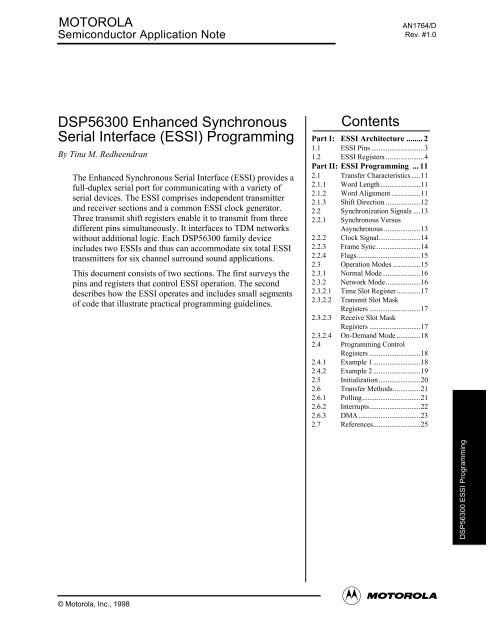
The Enhanced Synchronous Serial Interface (<strong>ESSI</strong>) provides a<br />
full-duplex serial port for communicating with a variety of<br />
serial devices. The <strong>ESSI</strong> comprises independent transmitter<br />
and receiver sections and a common <strong>ESSI</strong> clock generator.<br />
Three transmit shift registers enable it to transmit from three<br />
different pins simultaneously. It interfaces to TDM networks<br />
without additional logic. Each DSP56300 family device<br />
includes two <strong>ESSI</strong>s and thus can accommodate six total <strong>ESSI</strong><br />
transmitters for six channel surround sound applications.<br />
This document consists of two sections. The first surveys the<br />
pins and registers that control <strong>ESSI</strong> operation. The second<br />
describes how the <strong>ESSI</strong> operates and includes small segments<br />
of code that illustrate practical programming guidelines.<br />
© Motorola, Inc., 1998<br />
Contents<br />
AN1764/D<br />
Rev. #1.0<br />
Part I: <strong>ESSI</strong> Architecture ........ 2<br />
1.1 <strong>ESSI</strong> Pins .............................3<br />
1.2 <strong>ESSI</strong> Registers .....................4<br />
Part II: <strong>ESSI</strong> <strong>Programming</strong> ... 11<br />
2.1 Transfer Characteristics.....11<br />
2.1.1 Word Length......................11<br />
2.1.2 Word Alignment ................11<br />
2.1.3 Shift Direction ...................12<br />
2.2 Synchronization Signals ....13<br />
2.2.1 Synchronous Versus<br />
Asynchronous ....................13<br />
2.2.2 Clock Signal.......................14<br />
2.2.3 Frame Sync ........................14<br />
2.2.4 Flags...................................15<br />
2.3 Operation Modes ...............15<br />
2.3.1 Normal Mode.....................16<br />
2.3.2 Network Mode...................16<br />
2.3.2.1 Time Slot Register .............17<br />
2.3.2.2 Transmit Slot Mask<br />
Registers ............................17<br />
2.3.2.3 Receive Slot Mask<br />
Registers ............................17<br />
2.3.2.4 On-Demand Mode .............18<br />
2.4 <strong>Programming</strong> Control<br />
Registers ............................18<br />
2.4.1 Example 1 ..........................18<br />
2.4.2 Example 2 ..........................19<br />
2.5 Initialization.......................20<br />
2.6 Transfer Methods...............21<br />
2.6.1 Polling................................21<br />
2.6.2 Interrupts............................22<br />
2.6.3 DMA..................................23<br />
2.7 References..........................25<br />
DSP56300 <strong>ESSI</strong> <strong>Programming</strong>
Part 1 <strong>ESSI</strong> Architecture<br />
All DSP56300 devices contain two independent and identical Enhanced Synchronous Serial<br />
Interfaces, <strong>ESSI</strong>0 and <strong>ESSI</strong>1. For simplicity, this section describes a single generic interface.<br />
Figure 1-1 shows the <strong>ESSI</strong> block diagram, depicting the pins and registers that control <strong>ESSI</strong><br />
operation.<br />
Interrupts<br />
RSMA<br />
RSMB<br />
TSMA<br />
TSMB<br />
CRA<br />
CRB<br />
TSR<br />
SSISR<br />
Figure 1-1.<br />
GDB DDB<br />
RCLK<br />
TCLK<br />
Clock/Frame Sync Generators and Control Logic<br />
<strong>ESSI</strong> Block Diagram<br />
RX SHIFT REG<br />
Motorola DSP56300 <strong>ESSI</strong> <strong>Programming</strong> 2<br />
RX<br />
TX0 SHIFT REG<br />
TX0<br />
TX1 SHIFT REG<br />
TX1<br />
TX2 SHIFT REG<br />
TX2<br />
SRD<br />
STD<br />
SC0<br />
SC1<br />
SC2<br />
SCK<br />
AA0678
1.1 <strong>ESSI</strong> Pins<br />
Figure 1-2 depicts the <strong>ESSI</strong> pins.<br />
¥<br />
¥<br />
¥<br />
Enhanced<br />
Synchronous Serial<br />
Interface Port (<strong>ESSI</strong>)<br />
Figure 1-2.<br />
SC0-SC2<br />
SCK<br />
SRD<br />
STD<br />
<strong>ESSI</strong> Pins<br />
<strong>ESSI</strong> Pins<br />
Serial Control Pin 0 (SC0) - Provides many different functions depending on the mode<br />
settings, which are determined by the SYN, TE1, and SCD0 bits in Control Register A (CRA).<br />
Table 1-1 shows the various functions. This pin also functions as GPIO pin P0.<br />
Table 1-1: SC0 Operation<br />
SYN TE1 SCD0 Operation<br />
1 (Sync) 0 (Disable) 0 (Input) Flag 0 input<br />
1 (Sync) 0 (Disable) 1 (Output) Flag 0 output<br />
1 (Sync) 1 (Enable) - Transmitter 1 data (always an output)<br />
0 (Async) - 0 (Input) Receive clock input (external)<br />
0 (Async) - 1 (Output) Receive clock output (internal)<br />
Serial Control Pin 1 (SC1) - Provides many different functions depending on the mode<br />
settings, which are determined by the SYN, TE1, SSC1, and SCD0 bits in Control Register A<br />
(CRA). Table 1-2 shows the various functions. This pin also functions as GPIO pin P1.<br />
Table 1-2: SC1 Operation<br />
SYN TE2 SCD1 SSC1 Operation<br />
1 (Sync) 0 (Disable) 0 (Input) 0 (Flag) Flag 1 input<br />
1 (Sync) 0 (Disable) 1 (Output) 0 (Flag) Flag 1 output<br />
1 (Sync) 1 (Enable) - - Transmitter 2 data (always an output)<br />
1 (Sync) 0 (Disable) 0 (Input) 1 (TX0 Act) Reserved<br />
1 (Sync) 0 (Disable) 1 (Output) 1 (TX0 Act) TX0 active<br />
Port C/D GPIO<br />
P0 - P2<br />
P3<br />
P4<br />
P5<br />
0 (Async) - 0 (Input) - Receive frame sync input (external)<br />
0 (Async) - 1 (Output) - Receive frame sync output (internal)<br />
Serial Control Pin 2 (SC2) - Provides the serial frame sync for the <strong>ESSI</strong>. This pin has many<br />
different functions depending on the mode settings, which are determined by the SYN and<br />
Motorola <strong>ESSI</strong> Architecture 3
<strong>ESSI</strong> Registers<br />
¥<br />
¥<br />
¥<br />
SCD2 bits in Control Register A (CRA). Table 1-3 shows the various functions. This pin also<br />
functions as GPIO pin P2.<br />
Serial Clock Pin (SCK) - Provides the serial bit rate clock for the <strong>ESSI</strong>. This pin has many<br />
different functions depending on the mode settings, which are determined by the SYN and<br />
SCKD bits in Control Register A (CRA). Table 1-4 shows the various functions. This pin also<br />
functions as GPIO pin P3.<br />
Serial Receive Data Pin (SRD) - Receives data and is always an input. This pin also<br />
functions as GPIO pin P4.<br />
Serial Transmit Data Pin (STD) - Transmits data from transmitter 0 and is always an output.<br />
This pin also functions as GPIO pin P5.<br />
1.2 <strong>ESSI</strong> Registers<br />
Table 1-3: SC2 Operation<br />
SYN SCD2 Operation<br />
1 (Sync) 0 (Input) Transmit and receive frame sync input (external)<br />
1 (Sync) 1 (Output) Transmit and receive frame sync output (internal)<br />
0 (Async) 0 (Input) Transmit frame sync input (external)<br />
0 (Async) 1 (Output) Transmit frame sync output (internal)<br />
Table 1-4: SCK Operation<br />
SYN SCKD Operation<br />
1 (Sync) 0 (Input) Transmit and receive clock input (external)<br />
1 (Sync) 1 (Output) Transmit and receive clock output (internal)<br />
0 (Async) 0 (Input) Transmit clock input (external)<br />
0 (Async) 1 (Output) Transmit clock output (internal)<br />
The following registers control <strong>ESSI</strong> operation:<br />
¥ Control Register A (CRA) Ñ One of two registers that control <strong>ESSI</strong> operation (see<br />
Table 1-5).<br />
¥ Control Register B (CRB) Ñ Second of two registers that control <strong>ESSI</strong> operation (see<br />
Table 1-6).<br />
¥ Status Register (SSISR) Ñ A read-only register that describes the <strong>ESSI</strong> status and serial<br />
flags (see Table 1-7).<br />
¥ Transmit Slot Mask Register A (TSMA) and Transmit Slot Mask Register B (TSMB) Ñ<br />
Two registers that, in network mode, determine whether to transmit during a given time slot or<br />
to tri-state the transmitter. TSMA and TSMB together form one register, TSM. When bit n of<br />
TSM is cleared, the transmit data pins of the enabled transmitters are tri-stated during time slot<br />
n.<br />
When bit n of TSM is set, the transmit sequence proceeds normally during time slot n.<br />
Motorola DSP56300 <strong>ESSI</strong> <strong>Programming</strong> 4
<strong>ESSI</strong> Registers<br />
¥ Receive Slot Mask Register A (RSMA) and Receive Slot Mask Register B (RSMB) - Two<br />
registers that, in network mode, determine whether to receive during a given time slot or<br />
tri-state the receiver. RSMA and RSMB together form one register, RSM. When bit n of RSM<br />
is cleared, the receive data pin of the receiver is tri-stated during time slot n.<br />
When bit n of<br />
RSM is set, the receive sequence proceeds normally during time slot n.<br />
¥ Time Slot Register (TSR) - A write-only null data register that, in network mode, prevents<br />
data transmission for the current time slot.<br />
¥ Receive Data Register (RX) - A read-only register that accepts data from the receive shift<br />
register as it becomes full.<br />
¥ Transmit Data Registers (TX0, TX1, TX2) - A write-only register that transfers data to the<br />
transmit shift registers.<br />
The <strong>ESSI</strong> data registers are double buffered for maximum throughput. Data to be transmitted is written<br />
to a transmit data register. When the transmit data register is full, the data is automatically transferred<br />
to a transmit shift register and then shifted out to the transmit data pin. If data is shifted out of the<br />
transmit shift register but new data has not been written to the transmit data register and a transmit<br />
frame sync occurs, a transmit underrun error occurs. A receive shift register receives incoming data<br />
from the receive data pin. When the receive shift register is full, the data is automatically transferred to<br />
the receive data register. If data is shifted into the receive shift register but the previous data has not<br />
been read from the receive data register and a receive frame sync occurs, a receive overrun error<br />
occurs.<br />
Bit No. Bit Abbr. Value Function<br />
7-0 PM[7:0]<br />
$0 - $FF<br />
Table 1-5: Control Register A (CRA)<br />
Prescale Modulus Select<br />
<strong>ESSI</strong> clock is divided by PM plus 1<br />
10-8 - Reserved bits to be written with 0<br />
11 PSR<br />
16-12 DC[4:0]<br />
0<br />
1<br />
00000-11111<br />
00000<br />
00001-11111<br />
Prescaler Range<br />
<strong>ESSI</strong> clock is divided by eight<br />
<strong>ESSI</strong> clock is divided by one<br />
Frame Rate Divider Control<br />
In normal mode, equals the divide ratio minus 1<br />
In network mode, enables on-demand mode<br />
17 - Reserved bits to be written with 0<br />
18 ALC<br />
0<br />
1<br />
In network mode, equals the number of time slots per frame minus 1<br />
Alignment Control<br />
Align data to bit 23<br />
Align data to bit 15, not allowed with 24- and 32-bit word lengths<br />
Motorola <strong>ESSI</strong> Architecture 5
<strong>ESSI</strong> Registers<br />
Bit No. Bit Abbr. Value Function<br />
21-19 WL[2:0]<br />
22 SSC1<br />
000<br />
001<br />
010<br />
011<br />
100<br />
101<br />
11x<br />
0<br />
1<br />
Word Length Control<br />
8 bits per word<br />
12 bits per word<br />
16 bits per word<br />
24 bits per word<br />
32 bits per word (valid in the first 24 bits)<br />
32 bits per word (valid in the last 24 bits)<br />
Reserved<br />
Select SC1 as TX0 active - Valid only in synchronous mode with transmitter 2<br />
disabled (see Table 1-2)<br />
SC1 is Flag 1<br />
23 - Reserved bit to be written with 0<br />
Bit No. Bit Abbr. Value Function<br />
0 OF0<br />
1 OF1<br />
2 SCD0<br />
3 SCD1<br />
4 SCD2<br />
-<br />
-<br />
0<br />
1<br />
0<br />
1<br />
0<br />
1<br />
Table 1-5: Control Register A (CRA)<br />
SC1 is TX0 active - Valid only if SC1 is configured as an input; drives an external<br />
buffer for the transmitter 0<br />
Table 1-6: Control Register B (CRB)<br />
Serial Output Flag 0 - Valid only in synchronous mode with transmitter 1 disabled<br />
and SC0 configured as an output (see Table 1-1)<br />
Data written to OF0 is seen on the SC0 pin<br />
Serial Output Flag 1 - Valid only in synchronous mode with transmitter 2 disabled<br />
and SC1 configured as an output (see Table 1-2)<br />
Data written to OF1 is seen on the SC1 pin<br />
Serial Control Direction 0 - Not valid when transmitter 1 is enabled (see Table 1-1)<br />
SC0 is an input<br />
SC0 is an output<br />
Serial Control Direction 1 - Not valid when transmitter 2 is enabled (see Table 1-2)<br />
SC1 is an input<br />
SC1 is an output<br />
Serial Control Direction 2 (see Table 1-3)<br />
SC2 is an input<br />
SC2 is an output<br />
Motorola DSP56300 <strong>ESSI</strong> <strong>Programming</strong> 6
Bit No. Bit Abbr. Value Function<br />
5 SCKD<br />
6 SHFD<br />
8-7 FSL[1:0]<br />
0<br />
1<br />
0<br />
1<br />
00<br />
01<br />
Clock Source Direction (see Table 1-4)<br />
SCK is input, clock<br />
SCK is output, clock<br />
Shift Direction<br />
Shift MSB first<br />
Shift LSB first<br />
Frame Sync Length<br />
Receive Transmit<br />
Word length Word length<br />
Word length Bit length<br />
10 Bit length Bit length<br />
11 Bit length Word length<br />
9 FSR Frame Sync Relative Timing - Only valid with word length frame syncs<br />
0 Frame sync begins with first bit of data word<br />
1 Frame sync begins one bit before first bit of data word<br />
10 FSP Frame Sync Polarity<br />
0 Frame sync polarity is positive<br />
1 Frame sync polarity is negative<br />
11 CKP Clock Polarity<br />
<strong>ESSI</strong> Registers<br />
0 Data and frame sync are clocked out on the rising edge of the transmit clock and<br />
latched in on the falling edge of the receive clock<br />
1 Data and frame sync are clocked out on the falling edge of the transmit clock and<br />
latched in on the rising edge of the receive clock<br />
12 SYN Synchronous/Asynchronous<br />
0 Asynchronous mode<br />
1 Synchronous mode<br />
13 MOD <strong>ESSI</strong> Mode Select<br />
0<br />
1<br />
Table 1-6: Control Register B (CRB) (Continued)<br />
Normal mode<br />
Network mode<br />
14 TE2 Transmit 2 Enable - Valid only in synchronous mode<br />
0 Transmit 2 disabled<br />
1 Transmit 2 enabled<br />
Motorola <strong>ESSI</strong> Architecture 7
<strong>ESSI</strong> Registers<br />
Bit No. Bit Abbr. Value Function<br />
15 TE1 Transmit 1 Enable - Valid only in synchronous mode<br />
0 Transmit 1 disabled<br />
1 Transmit 1 enabled<br />
16 TE0 Transmit 0 Enable<br />
0 Transmit 0 disabled<br />
1 Transmit 0 enabled<br />
17 RE Receive Enable<br />
Table 1-6: Control Register B (CRB) (Continued)<br />
0 Receive disabled<br />
1 Receive enabled<br />
18 TIE Transmit Interrupt Enable<br />
0 Interrupt disabled<br />
1 Interrupt enabled<br />
19 RIE Receive Interrupt Enable<br />
0 Interrupt disabled<br />
1 Interrupt enabled<br />
20 TLIE Transmit Last Slot Interrupt Enable<br />
0 Interrupt disabled<br />
1 Interrupt enabled<br />
21 RLIE Receive Last Slot Interrupt Enable<br />
0 Interrupt disabled<br />
1 Interrupt enabled<br />
22 TEIE Transmit Exception Interrupt Enable<br />
0 Interrupt disabled<br />
1 Interrupt enabled<br />
23 REIE Receive Exception Interrupt Enable<br />
0 Interrupt disabled<br />
1 Interrupt enabled<br />
Motorola DSP56300 <strong>ESSI</strong> <strong>Programming</strong> 8
Bit No. Bit Abbr. Value Function<br />
Table 1-7: Status Register (SSISR)<br />
<strong>ESSI</strong> Registers<br />
0 IF0 Serial Input Flag 0 - Valid only in synchronous mode with transmitter 1 disabled<br />
and SC0 configured as an input (see Table 1-1)<br />
- Data on the SC0 pin is seen here.<br />
1 IF1 Serial Input Flag 1 - Valid only in synchronous mode with transmitter 1 disabled<br />
and SC1 configured as an input (see Table 1-2)<br />
- Data on the SC1 pin is seen here<br />
2 TFS Transmit Frame Sync Flag - Valid only if at least one transmitter is enabled<br />
Always = 1 in normal mode<br />
0 No transmit frame sync occurred during the current time slot<br />
1 Transmit frame sync occurred during the current time slot<br />
3 RFS Receive Frame Sync Flag - Valid only if the receiver is enabled<br />
Always = 1 in normal mode<br />
0 No receive frame sync occurred during the current time slot<br />
1 Receive frame sync occurred during the current time slot<br />
4 TUE Transmit Underrun Error Flag<br />
0 Otherwise<br />
1 At least one enabled transmit shift register is empty and a transmit time slot<br />
occurred<br />
5 ROE Receive Overrun Error Flag<br />
0 Otherwise<br />
1 Receive shift register is full but the receive data register is still full<br />
6 TDE Transmit Data Register Empty<br />
0 All enabled transmit data registers have been written to the DSP56300 core<br />
1 Enabled transmit data registers are transferred to the transmit shift registers, and<br />
data is ready for writing to the transmit data register<br />
7 RDF Receive Data Register Full<br />
0 Receive data register is read<br />
1 Receive shift register is transferred to the receive data register, and data is ready for<br />
reading from the receive data register<br />
In addition to the <strong>ESSI</strong> registers, the three following port registers control <strong>ESSI</strong> GPIO functionality.<br />
Port C is <strong>ESSI</strong>0 and Port D is <strong>ESSI</strong>1.<br />
¥ Port Control Register (PCRC & PCRD) Ñ Control the functionality of the <strong>ESSI</strong> GPIO<br />
signals. Each of the five bits in the port control registers controls the functionality of the<br />
corresponding port signal pin. When a bit is set, the corresponding port signal is configured as<br />
an <strong>ESSI</strong> signal. When a bit is clear, the corresponding port signal is configured as a GPIO<br />
signal.<br />
Motorola <strong>ESSI</strong> Architecture 9
<strong>ESSI</strong> Registers<br />
¥ Port Direction Register (PRRC & PRRD) - Control the direction of the <strong>ESSI</strong> GPIO signals.<br />
Each of the five bits in the port direction registers controls the direction of the corresponding<br />
port signal pin if the pin is configured as a GPIO signal. When a bit is set, the corresponding<br />
port signal is configured as an output. When a bit is clear, the corresponding port signal is<br />
configured as an input.<br />
¥ Port Data Register (PDRC & PDRD) - Read/write data to/from the <strong>ESSI</strong> GPIO signals. If a<br />
port signal is configured as a GPIO input, the corresponding bit reflects the value present on<br />
the pin. If a port signal is configured as a GPIO output, the value written into the<br />
corresponding bit is reflected on the pin.<br />
Motorola DSP56300 <strong>ESSI</strong> <strong>Programming</strong> 10
Part 2 <strong>ESSI</strong> <strong>Programming</strong><br />
Transfer Characteristics<br />
This section describes the practical operation of the <strong>ESSI</strong>, covering transfer characteristics,<br />
synchronization signals, operation modes, initialization method, and transfer methods. In some cases,<br />
segments of code illustrate practical programming guidelines. The code in this section uses equate<br />
labels for the location of the <strong>ESSI</strong> registers. These labels include the register name preceded with<br />
ÒM_Ó and can be found in the ioequ.asm file.<br />
2.1 Transfer Characteristics<br />
Words transferred by the <strong>ESSI</strong> are characterized by word length, shift direction, and word alignment.<br />
This section describes these characteristics and the programming associated with them.<br />
2.1.1 Word Length<br />
The <strong>ESSI</strong> presents six options for the number of bits per word or the word length. To choose word<br />
length, set the WL[2:0] bits in Control Register A (CRA[21:19]) as shown in Table 2-1.<br />
The <strong>ESSI</strong><br />
transmit and receive data registers are 24-bits long, so 32-bits words cannot be completely transmitted<br />
or received. For 32-bit words, two options are available: the first 24 bits contain valid data and the last<br />
bit is duplicated eight times, or the last 24 bits contain valid data and the first bit is duplicated eight<br />
times.<br />
2.1.2 Word Alignment<br />
Table 2-1: Word Length<br />
WL2 WL1 WL0 Number of Bits per Word<br />
0 0 0 8<br />
0 0 1 12<br />
0 1 0 16<br />
0 1 1 24<br />
1 0 0 32 (data valid in the first 24 bits)<br />
1 0 1 32 (data valid in the last 24 bits)<br />
1 1 0 Reserved<br />
1 1 1 Reserved<br />
Words less than 24-bits long can be aligned in two ways based on the value of CRA[18], ALC. If ALC<br />
is set, 8-, 12-, and 16-bit words are left-aligned to bit 15. If ALC is clear, 8-, 12-, and 16-bit words are<br />
left-aligned to bit 23. Figure 2-3 shows the different options for the word alignment.<br />
Motorola DSP56300 <strong>ESSI</strong> <strong>Programming</strong> 11
Transfer Characteristics<br />
CRA: ALC = 0,<br />
Align to bit 23<br />
CRA: ALC = 1,<br />
Align to bit 15<br />
2.1.3 Shift Direction<br />
8-bit<br />
12-bit<br />
16-bit<br />
Figure 2-3.<br />
Alignment Control<br />
The <strong>ESSI</strong> presents two options for shift direction: Most Significant Bit (MSB) first or Least<br />
Significant Bit (LSB) first. To select shift direction, set bit 6 in Control Register B (CRB[6]), SHFD. If<br />
SHFD is set, the data is shifted into the receive shift register from the SRD pin and out of the transmit<br />
shift register to the STD pin with the LSB first. If SHFD is clear, the data is shifted into the receive<br />
shift register from the SRD pin and out of the transmit shift register to the STD pin with the MSB first.<br />
Figure 2-4 shows how data is shifted for both shift direction options.<br />
STD<br />
TX Data Register<br />
TX Shift Register<br />
bit 23<br />
TX Data Register<br />
TX Shift Register<br />
Data Registers<br />
bit 15<br />
Figure 2-4.<br />
8-bit<br />
12-bit<br />
16-bit<br />
CRB: SHFD = 0, MSB first<br />
CRB: SHFD = 1, LSB first<br />
STD<br />
Shift Direction<br />
Motorola DSP56300 <strong>ESSI</strong> <strong>Programming</strong> 12<br />
SRD<br />
bit 0<br />
bit 0<br />
RX Data Register<br />
RX Shift Register<br />
SRD<br />
RX Data Register<br />
RX Shift Register
2.2 Synchronization Signals<br />
Synchronization Signals<br />
Because the <strong>ESSI</strong> is a synchronous interface, it requires clock and frame sync signals to define when<br />
the data changes and when a new frame begins. In certain modes, the <strong>ESSI</strong> also has the option of two<br />
flag signals to use for device selection. This section describes all of these signals.<br />
2.2.1 Synchronous Versus Asynchronous<br />
The <strong>ESSI</strong> includes both synchronous and asynchronous modes. In synchronous mode, the transmitters<br />
and receiver use the same clock and frame sync; in asynchronous mode, the transmitters and receiver<br />
use different clocks and frame syncs. The <strong>ESSI</strong> data transfers are synchronized to a clock in both<br />
modes. The choice of synchronous versus asynchronous mode is determined by the SYN bit,<br />
CRB[12]. Setting SYN puts the <strong>ESSI</strong> is in synchronous mode; clearing SYN puts it in asynchronous<br />
mode. Figure 2-5 summarizes the operation of the <strong>ESSI</strong> pins in synchronous and asynchronous<br />
modes.<br />
SYN = 1, Synchronous mode<br />
SCK<br />
STD<br />
SRD<br />
SC2<br />
SC1<br />
SC0<br />
Clock<br />
Transmit<br />
Receive<br />
Frame Sync<br />
Flag 1 or Transmit 2<br />
Flag 0 or Transmit 1<br />
Figure 2-5.<br />
SYN = 0, Asynchronous mode<br />
Synchronous Versus Asynchronous<br />
In synchronous mode:<br />
¥ SCK is an input or an output that all enabled transmitters and the receiver use as the clock<br />
signal.<br />
¥ SC2 is an input or an output that all enabled transmitters and the receiver use as the frame sync<br />
signal.<br />
¥ SC0 and SC1 can be used as extra transmitter signals or as flag signals.<br />
In asynchronous mode1<br />
:<br />
¥ SCK is an input or an output that transmitter 0 uses as the clock signal.<br />
¥ SC2 is an input or an output that all enabled transmitters use as the frame sync signal.<br />
¥ SC0 is an input or an output that the receiver uses as the clock signal.<br />
¥ SC1 is an input or an output that the receiver uses as the frame sync signal.<br />
1. Transmitters 1 and 2 and Flags 0 and 1 cannot be used in asynchronous mode.<br />
Motorola DSP56300 <strong>ESSI</strong> <strong>Programming</strong> 13<br />
SCK<br />
STD<br />
SRD<br />
SC2<br />
SC1<br />
SC0<br />
Transmit Clock<br />
Transmit<br />
Receive<br />
Transmit Frame Sync<br />
Receive Clock<br />
Receive Frame Sync
Synchronization Signals<br />
The direction of the SC0, SC1, SC2, and SCK pins is determined by the SCD0, SCD1, SCD2, and<br />
SCKD bits, respectively, CRB[2:5]. If one of these bits is clear, the corresponding pin is an input. If<br />
one of these bits is set, the corresponding pin is an output.<br />
2.2.2 Clock Signal<br />
When the SCK pin is an output (SCKD = 1), its rate is controlled by two sets of bits in CRA, PSR, and<br />
PM[7:0], as Figure 2-6 shows.<br />
F CORE<br />
Figure 2-6.<br />
Clock Generation<br />
The maximum <strong>ESSI</strong> clock frequency is FCORE<br />
/ 4. The PSR = 1 and PM[7:0] = $00 to give FCORE<br />
/ 2<br />
should not be used. The minimum <strong>ESSI</strong> clock frequency is FCORE<br />
/ (2*8*256) = FCORE<br />
/ 4096. The<br />
polarity of the clock signal is determined by CRB[11], CKP. If CKP is clear, the data and the frame<br />
sync are clocked out on the rising edge of the transmit clock and latched in on the falling edge of the<br />
receive clock. If CKP is set, the data and the frame sync are clocked out on the falling edge of the<br />
transmit clock and latched in on the rising edge of the receive clock.<br />
When SCK is an input (SCKD = 0), the internal clock generator is disconnected from the SCK pin and<br />
an external clock source can drive this pin.<br />
2.2.3 Frame Sync<br />
Divide<br />
by<br />
2<br />
Divide<br />
by<br />
1 or 8<br />
Divide<br />
by<br />
1 to 256<br />
PSR = PM[7:0] =<br />
1 or 0 0 to FF<br />
The frame sync signal indicates when a new frame begins. In synchronous mode, the SC2 pin is the<br />
frame sync for the receiver and all enabled transmitters. In asynchronous mode, SC2 is the frame sync<br />
signal for the receiver and SC0 is the frame sync signal for transmitter 0. The direction of the frame<br />
sync pins is determined by the SCD0 or SCD2 bits in CRB. If either of these bits is clear, the<br />
corresponding pin is an input. If either of these bits is set, the corresponding pin is an output.<br />
The frame sync is characterized by its length and position. The length of the frame sync is specified by<br />
the FSL[1:0] bits, CRB[7:8], as shown in Table 2-2.<br />
The frame sync length must be the same for the<br />
transmitter and the receiver (FSL[1:0] = 00 or 10) when the <strong>ESSI</strong> is in synchronous mode because the<br />
transmitter and receiver share a frame sync signal. A bit length frame sync is required in normal mode<br />
(MOD = 0) with a divide ratio of 1 (DC[4:0] = 00000) because this mode provides continuous data<br />
transfers.<br />
Motorola DSP56300 <strong>ESSI</strong> <strong>Programming</strong> 14<br />
SCK
Operation Modes<br />
Word length frame syncs can be positioned two ways based on the value of CRB[9], FSR. If FSR is<br />
clear, the word length frame sync occurs together with the first bit of the data word in the first time<br />
slot. If FSR is set, the word length frame sync occurs one clock cycle before the first bit in the data<br />
word of the first time slot.<br />
The polarity of the frame sync signals is determined by CRB[10], FSP. If FSP is clear, the frame sync<br />
is positive, i.e. the frame sync goes high to indicate a frame start. If FSP is set, the frame sync is<br />
negative, i.e. the frame sync goes low to indicate a frame start.<br />
2.2.4 Flags<br />
FSL1 FSL0<br />
When the <strong>ESSI</strong> is in synchronous mode and transmitters 1 and 2 are disabled, the SC0 and SC1 pins<br />
are available for use as flags. The following rules apply for the flag signals:<br />
If SC0 is an:<br />
¥ input (SCD0 = 0), data on the SC0 pin is seen on SSISR[0], IF0.<br />
¥ output (SCD0 = 1), data written to OF0, CRB[0], is seen on the SC0 pin.<br />
If SC1 is an:<br />
¥ input (SCD1 = 0), data on the SC1 pin is seen on SSISR[1], IF1.<br />
¥ output (SCD1 = 1), data written to OF1, CRB[1], is seen on the SC1 pin.<br />
The flags can change at the beginning of each frame in normal mode and at the beginning of each time<br />
slot in network mode.<br />
There is one additional option for the SC1 pin. In synchronous mode with transmitter 2 disabled, the<br />
SC1 pin can be programmed as a transmitter 0 active signal. When the TX0 active pin is high,<br />
transmitter 0 is active; when this pin is low, transmitter 0 is not active. This signal can enable an<br />
external buffer for the transmitter 0 output. This option is selected using CRA[22], SSC1, which is<br />
valid only in synchronous mode with transmitter 2 disabled. If SSC1 is clear, SC1 is the flag 0 signal.<br />
If SSC1 is set, SC1 is the transmitter 0 active signal.<br />
2.3 Operation Modes<br />
Table 2-2: Frame Sync Length<br />
Frame Sync Length<br />
RX TX<br />
0 0 Word Word<br />
0 1 Word Bit<br />
1 0 Bit Bit<br />
1 1 Bit Word<br />
The <strong>ESSI</strong> has three basic modes of operation: normal, network, and on-demand. The operation mode is<br />
selected by the MOD bit, CRB[11]. If MOD is clear, the <strong>ESSI</strong> is normal mode. If MOD is set, the<br />
<strong>ESSI</strong> is in network mode. Additionally, the on-demand mode is selected if MOD is set and the<br />
DC[4:0] bits in CRA are all clear. The following sections describe each of the operation modes.<br />
Motorola DSP56300 <strong>ESSI</strong> <strong>Programming</strong> 15
Operation Modes<br />
2.3.1 Normal Mode<br />
The normal mode of operation has one time slot per frame. Thus, one data word is transferred for<br />
every frame sync. However, the data word does not have to fill the entire frame. The DC[4:0] bits in<br />
CRA define the divide ratio minus one. The divide ratio can be interpreted as the frame length divided<br />
by the data length, as Figure 2-7 shows. This ratio can be between 1 and 32 (DC[4:0] = 00000 to<br />
11111).<br />
Frame Sync Signal (with word length frame sync)<br />
Data Signal<br />
Data Data Data<br />
Data Length<br />
Frame Length<br />
2.3.2 Network Mode<br />
Figure 2-7.<br />
Normal Mode Frame Divider Control<br />
The network mode of operation allows more than one time slot per frame. Up to 32 data words can be<br />
transferred for every frame sync. The DC[4:0] bits in CRA define the number of time slots per frame<br />
minus one. Figure 2-8 illustrates the number of time slots per frame, which can be between 2 and 32<br />
(DC[4:0] = 00001 to 11111). DC[4:0] = 00000 is reserved for on-demand mode.<br />
Frame Sync Signal (with word length frame sync)<br />
Data Signal<br />
Figure 2-8.<br />
Network Mode Frame Divider Control<br />
Divide Ratio = Frame Length / Data Length<br />
Data Data Data Data Data Data Data Data Data<br />
Time Slot 1<br />
Time Slot 2<br />
Time Slot 3<br />
Time Slot N<br />
Number of Time Slots per Frame = N<br />
Motorola DSP56300 <strong>ESSI</strong> <strong>Programming</strong> 16
Operation Modes<br />
Some applications do not require data to be transmitted or received during every time slot. There are<br />
two types of registers that control which time slots receive and transmit data: the time slot register and<br />
the slot mask registers.<br />
2.3.2.1 Time Slot Register<br />
The time slot register (TSR) is a write-only null data register that prevents data transmission in the<br />
current time slot. TSR is similar to a transmit data register. However, when data is written to the TSR,<br />
the data is not transmitted. Instead, all of the enabled transmitters are in the high-impedance state for<br />
the current time slot. The following code writes an arbitrary data word to the time slot registers for<br />
<strong>ESSI</strong>0 and <strong>ESSI</strong>1 to disable transmission during the current time slot:<br />
movep #data,x:M_TSR0 ;Write data to <strong>ESSI</strong>0 TSR0 reg - disable TX<br />
movep #data,x:M_TSR1 ;Write data to <strong>ESSI</strong>0 TSR1 reg - disable TX<br />
2.3.2.2 Transmit Slot Mask Registers<br />
There are two transmit slot mask registers, Transmit Slot Mask Register A (TSMA) and Transmit Slot<br />
Mask Register B (TSMB). Both TSMA and TSMB are 16 bits wide. Together they can be regarded as<br />
one 32-bit register, TSM. When bit n of the TSM is set, the transmit sequence proceeds normally<br />
during time slot n.<br />
When bit n of the TSM is cleared, the transmit data pins of the enabled transmitters<br />
are tri-stated during time slot n.<br />
Also, when bit n of TSM is cleared, the TDE and TUE flags in the<br />
SSISR are not set during time slot n.<br />
Thus, transmit interrupts are generated only for enabled time<br />
slots. The transmit slot mask registers do not conflict with the TSR register. Even if a time slot is<br />
enabled in the transmit slot mask registers, writing to the TSR disables the transmitters.<br />
The following code writes to the transmit slot mask registers for <strong>ESSI</strong>0 and <strong>ESSI</strong>1 to disable<br />
transmission during all except the first and the fourth time slots. To ensure that this code runs properly,<br />
verify that the DC[4:0] bits are set so that there are at least four time slots per frame.<br />
movep #0009,x:M_TSMA0 ;Load TSMA for <strong>ESSI</strong>0<br />
movep #0000,x:M_TSMB0 ;Load TSMB for <strong>ESSI</strong>0<br />
movep #0009,x:M_TSMA1 ;Load TSMA for <strong>ESSI</strong>1<br />
movep #0000,x:M_TSMB1 ;Load TSMB for <strong>ESSI</strong>1<br />
2.3.2.3 Receive Slot Mask Registers<br />
There are two receive slot mask registers, Receive Slot Mask Register A (RSMA) and Receive Slot<br />
Mask Register B (RSMB). Both RSMA and RSMB are 16 bits wide. Together they can be regarded as<br />
one 32-bit register, RSM. When bit n of RSM is set, the transmit sequence proceeds normally during<br />
time slot n.<br />
When bit n of RSM is cleared, the receive data pins of the enabled transmitters are<br />
tri-stated during time slot n.<br />
Also, when bit n of RSM is cleared, the RDF and ROE flags in the SSISR<br />
are not set during time slot n.<br />
Thus, receive interrupts are generated only for enabled time slots.<br />
The following code writes to the receive slot mask registers so that <strong>ESSI</strong>0 receives only during the first<br />
time slot and <strong>ESSI</strong>1 receives only during the fourth time slot. To ensure that this code runs properly,<br />
verify that the DC[4:0] bits are set so that there are at least four time slots per frame.<br />
Motorola DSP56300 <strong>ESSI</strong> <strong>Programming</strong> 17
<strong>Programming</strong> Control Registers<br />
movep #0001,x:M_RSMA0 ;Load RSMA for <strong>ESSI</strong>0<br />
movep #0000,x:M_RSMB0 ;Load RSMB for <strong>ESSI</strong>0<br />
movep #0008,x:M_RSMA1 ;Load RSMA for <strong>ESSI</strong>1<br />
movep #0000,x:M_RSMB1 ;Load RSMB for <strong>ESSI</strong>1<br />
2.3.2.4 On-Demand Mode<br />
The on-demand mode of operation does not generate a periodic frame sync. Thus, no time slots are<br />
defined in this mode. A frame sync is generated only when data is ready to be transmitted, i.e. data is<br />
written to a transmit data register. The on-demand mode is selected if the MOD bit is set and the<br />
DC[4:0] bits in CRA are all clear. This mode requires that the transmit frame sync be internal (output)<br />
and the receive frame sync be external (input) for proper operation. Because the transmit and receive<br />
frame syncs must be opposite, only simplex operation (receive or transmit but not both) is allowed in<br />
synchronous mode. Duplex operation (receive and transmit simultaneously) is allowed only in<br />
asynchronous mode. Transmit underruns are impossible in on-demand mode because there are no<br />
transmit time slots. Thus transmit underruns are disabled.<br />
2.4 <strong>Programming</strong> Control Registers<br />
This section shows how to program the control registers, CRA and CRB, to achieve the characteristics<br />
described in previous sections of this document. Two examples are presented, including pinout<br />
diagrams and equates describing the control register settings.<br />
2.4.1 Example 1<br />
This example programs <strong>ESSI</strong>0 for normal asynchronous mode. Figure 2-9 shows the basic pinout<br />
diagram for this example. Recall that in asynchronous mode there are separate clock and frame sync<br />
signals for the transmit and receive transfers. The comments following the equates describe the other<br />
characteristics for this example.<br />
Figure 2-9.<br />
STD0<br />
SCK0<br />
SC02<br />
SRD0<br />
SC00<br />
SC01<br />
TX Data<br />
TX Clock<br />
TX Frame Sync<br />
RX Data<br />
RX Clock<br />
RX Frame Sync<br />
Normal Asynchronous Mode Example<br />
The following code sets up the equates for CRA and CRB, which initialize the <strong>ESSI</strong>.<br />
Motorola DSP56300 <strong>ESSI</strong> <strong>Programming</strong> 18
<strong>Programming</strong> Control Registers<br />
;-------------------------------------------------------------------------------<br />
CRA0 EQU $01F801<br />
; <strong>ESSI</strong>0 Control Register A, CRA<br />
; Bit 22 SSC1 0 SC1 pin = serial I/O flag<br />
; Bit 21-19 WL[2:0] 000 8 bits/word<br />
; Bit 18 ALC 0 Left align to bit 23<br />
; Bit 16-12 DC[4:0] 11111 Divide ratio = 32<br />
; Bit 11 PSR 1 Fixed prescaler bypassed<br />
; Bit 7-0 PM[7:0] 00000001 Clock divide = 2<br />
;-------------------------------------------------------------------------------<br />
CRB0 EQU $C80DCC<br />
; <strong>ESSI</strong>0 Control Register B, CRB<br />
; Bit 23 REIE 1 RX exception int enabled<br />
; Bit 22 TEIE 1 TX exception int enabled<br />
; Bit 21 RLIE 0 RX last slot int disabled<br />
; Bit 20 TLIE 0 TX last slot int disabled<br />
; Bit 19 RIE 1 RX int enabled<br />
; Bit 18 TIE 0 TX int disabled<br />
; Bit 17 RE 0 RX disabled<br />
; Bit 16 TE0 0 TX0 disabled<br />
; Bit 15 TE1 0 TX1 disabled<br />
; Bit 14 TE2 0 TX2 disabled<br />
; Bit 13 MOD 0 Normal mode<br />
; Bit 12 SYN 0 Asynchronous mode<br />
; Bit 11 CKP 1 Clk polarity on falling edge<br />
; Bit 10 FSP 1 Frame sync polarity negative<br />
; Bit 9 FSR 0 Frame sync with 1st bit<br />
; Bit 8-7 FSL 11 Word length TX frame sync<br />
; Bit length RX frame sync<br />
; Bit 6 SHFD 1 Shift LSB first<br />
; Bit 5 SCKD 0 External clock source<br />
; Bit 4 SCD2 0 SC2 pin = input<br />
; Bit 3 SCD1 1 SC1 pin = output<br />
; Bit 2 SCD0 1 SC0 pin = output<br />
; Bit 1-0 OF[1:0] 00 Output flags<br />
2.4.2 Example 2<br />
This example programs <strong>ESSI</strong>1 for network synchronous mode. Figure 2-10 shows the basic pinout<br />
diagram for this example. SC11 is the TX0 active signal. The comments following the equates<br />
describe the other characteristics for this example.<br />
Figure 2-10.<br />
STD1<br />
SCK1<br />
SC12<br />
SRD1<br />
SC10<br />
SC11<br />
TX Data<br />
Clock<br />
Frame Sync<br />
RX Data<br />
Flag 0<br />
TX0 Active<br />
Network Synchronous Mode Example<br />
The following code sets up the equates for CRA and CRB, which initialize the <strong>ESSI</strong>.<br />
Motorola DSP56300 <strong>ESSI</strong> <strong>Programming</strong> 19
Initialization<br />
CRA1 EQU $505803<br />
; <strong>ESSI</strong>1 Control Register A, CRA<br />
; Bit 22 SSC1 1 SC1 pin = TX0 active<br />
; Bit 21-19 WL[2:0] 010 16 bits/word<br />
; Bit 18 ALC 0 Left align to bit 23<br />
; Bit 16-12 DC[4:0] 00101 Number of time slots = 6<br />
; Bit 11 PSR 1 Fixed prescaler bypassed<br />
; Bit 7-0 PM[7:0] 00000011 Clock divide = 4<br />
;-------------------------------------------------------------------------------<br />
CRB1 EQU $FC357C<br />
; <strong>ESSI</strong>1 Control Register B, CRB<br />
; Bit 23 REIE 1 RX exception int enabled<br />
; Bit 22 TEIE 1 TX exception int enabled<br />
; Bit 21 RLIE 1 RX last slot int enabled<br />
; Bit 20 TLIE 1 TX last slot int enabled<br />
; Bit 19 RIE 1 RX int enabled<br />
; Bit 18 TIE 1 TX int enabled<br />
; Bit 17 RE 0 RX disabled<br />
; Bit 16 TE0 0 TX0 disabled<br />
; Bit 15 TE1 0 TX1 disabled<br />
; Bit 14 TE2 0 TX2 disabled<br />
; Bit 13 MOD 1 Network mode<br />
; Bit 12 SYN 1 Synchronous mode<br />
; Bit 11 CKP 0 Clk polarity on rising edge<br />
; Bit 10 FSP 1 Frame sync polarity negative<br />
; Bit 9 FSR 0 Frame sync with 1st bit<br />
; Bit 8-7 FSL 10 Bit length frame sync<br />
; Bit 6 SHFD 1 Shift LSB first<br />
; Bit 5 SCKD 1 Internal clock source<br />
; Bit 4 SCD2 1 SC2 pin = output<br />
; Bit 3 SCD1 1 SC1 pin = output<br />
; Bit 2 SCD0 1 SC0 pin = output<br />
; Bit 1-0 OF[1:0] 00 Output flags<br />
2.5 Initialization<br />
Perform the following steps to initialize the <strong>ESSI</strong> properly:<br />
1. Reset the <strong>ESSI</strong>.<br />
This is accomplished by a hardware or software reset or by putting the <strong>ESSI</strong> into its individual<br />
reset state by clearing the PCR bits as shown here.<br />
movep #$0,x:M_PCRC ;Reset <strong>ESSI</strong>0<br />
movep #$0,x:M_PCRD ;Reset <strong>ESSI</strong>1<br />
2. Program the <strong>ESSI</strong> control registers.<br />
CRA and CRB must be programmed to control the <strong>ESSI</strong> operation. The following commands<br />
program the <strong>ESSI</strong> control registers by moving equates into CRA and CRB for both <strong>ESSI</strong>s.<br />
3. Enable the <strong>ESSI</strong> pins.<br />
movep #CRA0,x:M_CRA0 ;Load CRA for <strong>ESSI</strong>0<br />
movep #CRB0,x:M_CRB0 ;Load CRB for <strong>ESSI</strong>0<br />
movep #CRA1,x:M_CRA1 ;Load CRA for <strong>ESSI</strong>1<br />
movep #CRB1,x:M_CRB1 ;Load CRB for <strong>ESSI</strong>1<br />
Set the bits in the PCRC and PCRD registers that correspond to the <strong>ESSI</strong> pins to be used. The<br />
following commands set all of the Port C and Port D bits to enable all the <strong>ESSI</strong>0 and <strong>ESSI</strong>1 pins.<br />
Motorola DSP56300 <strong>ESSI</strong> <strong>Programming</strong> 20
movep #$3F,x:M_PCRC ;Enable <strong>ESSI</strong>0<br />
movep #$3F,x:M_PCRD ;Enable <strong>ESSI</strong>1<br />
4. Write the Þrst data to the transmit registers.<br />
Transfer Methods<br />
The first data word to be transmitted should be present in the transmit data registers before the<br />
transmitters are enabled (even if DMA is used to transfer data to the transmit register). The<br />
following commands write the first data to all the transmit data registers for both <strong>ESSI</strong>s.<br />
TX*_data1 represents any register or memory location that contains the first data to be<br />
transmitted.<br />
movep TX00_data1,x:M_TX00 ;Write first data to <strong>ESSI</strong>0 TX0 reg<br />
movep TX01_data1,x:M_TX01 ;Write first data to <strong>ESSI</strong>0 TX1 reg<br />
movep TX02_data1,x:M_TX02 ;Write first data to <strong>ESSI</strong>0 TX2 reg<br />
movep TX10_data1,x:M_TX10 ;Write first data to <strong>ESSI</strong>1 TX0 reg<br />
movep TX11_data1,x:M_TX11 ;Write first data to <strong>ESSI</strong>1 TX1 reg<br />
movep TX12_data1,x:M_TX12 ;Write first data to <strong>ESSI</strong>1 TX2 reg<br />
5. Enable the transmitters and receiver.<br />
Set the transmitter and receiver enable bits in CRB0 and CRB1 as follows.<br />
bset #14,x:M_CRB0 ;Enable <strong>ESSI</strong>0 TX2<br />
bset #15,x:M_CRB0 ;Enable <strong>ESSI</strong>0 TX1<br />
bset #16,x:M_CRB0 ;Enable <strong>ESSI</strong>0 TX0<br />
bset #14,x:M_CRB1 ;Enable <strong>ESSI</strong>1 TX2<br />
bset #15,x:M_CRB1 ;Enable <strong>ESSI</strong>1 TX1<br />
bset #16,x:M_CRB1 ;Enable <strong>ESSI</strong>1 TX0<br />
bset #17,x:M_CRB0 ;Enable <strong>ESSI</strong>0 RE<br />
bset #17,x:M_CRB1 ;Enable <strong>ESSI</strong>1 RE<br />
2.6 Transfer Methods<br />
The <strong>ESSI</strong> provides three methods for transferring data to or from the data registers: polling, interrupts,<br />
and DMA. Polling is the easiest method, but it demands a large amount of the DSP56300 coreÕs<br />
processing power. The DSP56300 core cannot be involved in other processing activities while it polls<br />
the receive and transmit ready bits. Interrupts, on the other hand, require more code, but the Core can<br />
process other routines while waiting for the <strong>ESSI</strong> transfers. DMA requires even less core intervention<br />
and the setup code is minimal, but the DMA channels must be available. The following sections<br />
describe each transfer method.<br />
2.6.1 Polling<br />
The SSISR provides bits that notify the core when data is ready to be transferred to or from the <strong>ESSI</strong>.<br />
The core can poll these bits to determine when to interact with the <strong>ESSI</strong>. For proper operation, the DSP<br />
core must write to the transmit buffer only when it is empty and read from the receive data register<br />
when it is full.<br />
SSISR[6], Transmit Data Register Empty (TDE), determines when to write to the transmit data<br />
registers. TDE is cleared when the core writes to all enabled transmit data registers. TDE is set when<br />
this data is transferred from the transmit data registers into the transmit shift registers. Thus, when<br />
TDE is set, the transmit data registers are empty and the core can write to the transmit data registers.<br />
The following code polls the TDE bit and writes to the transmit registers when this bit is set.<br />
TX*_data represents any register or memory location that contains the data to be transmitted.<br />
Motorola DSP56300 <strong>ESSI</strong> <strong>Programming</strong> 21
Transfer Methods<br />
jclr #6,x:M_SSISR0,* ;Wait until <strong>ESSI</strong>0 transmit registers are empty<br />
movep TX00_data,x:M_TX00 ;Write data to <strong>ESSI</strong>0 TX0 reg<br />
movep TX01_data,x:M_TX01 ;Write data to <strong>ESSI</strong>0 TX1 reg<br />
movep TX02_data,x:M_TX02 ;Write data to <strong>ESSI</strong>0 TX2 reg<br />
jclr #6,x:M_SSISR1,* ;Wait until <strong>ESSI</strong>1 transmit registers are empty<br />
movep TX10_data,x:M_TX10 ;Write data to <strong>ESSI</strong>1 TX0 reg<br />
movep TX11_data,x:M_TX11 ;Write data to <strong>ESSI</strong>1 TX1 reg<br />
movep TX12_data,x:M_TX12 ;Write data to <strong>ESSI</strong>1 TX2 reg<br />
SSISR[7], Receive Data Register Full (RDF), determines when to read from the receive data register.<br />
RDF is cleared when the core reads data from the receive data register. RDF is set when data is<br />
transferred from the receive shift register to the receive data register. Thus, when RDF is set, the<br />
receive data register is full and the core can read from the receive data register. The following code<br />
polls the RDF bit and reads from the receive register when this bit is set. RX*_data represents any<br />
register or memory location to which received data should be written.<br />
2.6.2 Interrupts<br />
jclr #7,x:M_SSISR0,* ;Wait until <strong>ESSI</strong>0 receive register is full<br />
movep x:M_RX0,RX0_data ;Read data from <strong>ESSI</strong>0 RX reg<br />
jclr #7,x:M_SSISR1,* ;Wait until <strong>ESSI</strong>1 receive register is full<br />
movep x:M_RX1,RX1_data ;Read data from <strong>ESSI</strong>1 RX reg<br />
The <strong>ESSI</strong> provides the following six interrupts, which are listed from highest to lowest priority:<br />
¥ Receive Data with Exception<br />
Ñ Enabled by setting CRB[23], REIE.<br />
Ñ Triggered when ROE (a receiver overrun error is detected), RDF (the receive data register<br />
is full) and REIE are set simultaneously.<br />
Ñ Cleared by reading from SSISR and then from RX.<br />
¥ Receive Data<br />
Ñ Enabled by setting CRB[19], RIE.<br />
Ñ Triggered when RDF (the receive data register is full) and RIE are set simultaneously.<br />
Ñ Cleared by reading from RX.<br />
¥ Receive Last Slot<br />
Ñ Enabled by setting CRB[21], RLIE.<br />
Ñ Triggered in network mode when RLIE is set and the last time slot ends.<br />
Ñ Maximum time to service this interrupt must be less than the time to service the number of<br />
bits in one time slot.<br />
¥ Transmit Data with Exception<br />
Ñ Enabled by setting CRB[22], TEIE.<br />
Ñ Triggered when TUE (a transmit underrun error has been detected), TDE (the transmit<br />
data register is empty) and TEIE are set simultaneously.<br />
Ñ Cleared by writing to SSISR and then by writing to all enabled TX registers or to TSR.<br />
Motorola DSP56300 <strong>ESSI</strong> <strong>Programming</strong> 22
Transfer Methods<br />
¥ Transmit Last Slot<br />
Ñ Enabled by setting CRB[20], TLIE.<br />
Ñ Triggered in network mode when TLIE is set and the last time slot is beginning.<br />
Ñ Maximum time to service this interrupt must be less than the time to service the number of<br />
bits in one time slot.<br />
¥ Transmit Data<br />
Ñ Enabled by setting CRB[18], TIE.<br />
Ñ Triggered when TDE (the transmit data register is empty) and TIE are set simultaneously.<br />
Ñ Cleared by writing to all enabled TX registers or to TSR.<br />
Configuring interrupts requires two steps: setting up the interrupt routine and enabling the interrupts.<br />
To set up the interrupt routine, place the code to be run during the interrupt at the interrupt starting<br />
address. The interrupt routines can be short (only two opcodes long) or long (more that two opcodes<br />
that requires a jsr instruction). Enabling the interrupts involves setting the corresponding bits in CRB<br />
and enabling the <strong>ESSI</strong> interrupts in the Interrupt Priority Register - Peripheral (IPRP) and enabling<br />
global interrupts in the Mode Register (MR) portion of the Status Register (SR).<br />
The following code sets up short interrupt routines to service the <strong>ESSI</strong>0 and <strong>ESSI</strong>1 transmitter 0 and<br />
receiver. This code uses equate labels for the location of the <strong>ESSI</strong> interrupt starting addresses. These<br />
labels include the interrupt name preceded with ÒI_Ó and can be found in the intequ.asm file.<br />
TX*_data represents any register or memory location that contains the data to be transmitted and<br />
RX*_data represents any register or memory location to which received data should be written.<br />
org p:I_SI0TD<br />
movep TX00_data,x:M_TX00 ;Write data to <strong>ESSI</strong>0 TX0 reg<br />
org p:I_SI1TD<br />
movep TX10_data,x:M_TX10 ;Write data to <strong>ESSI</strong>1 TX0 reg<br />
org p:I_SI0RD<br />
movep x:M_RX0,RX0_data ;Read data from <strong>ESSI</strong>0 RX reg<br />
org p:I_SI1RD<br />
movep x:M_RX1,RX1_data ;Read data from <strong>ESSI</strong>1 RX reg<br />
The following code enables the <strong>ESSI</strong>0 and <strong>ESSI</strong>1 transmit and receive interrupts. Instead of the first<br />
four commands, the interrupt enable bits in CRB can alternatively be set when CRB is initially<br />
programmed (as in Step 2 of Section 2.5).<br />
2.6.3 DMA<br />
bset #18,x:M_CRB0 ;Enable <strong>ESSI</strong>0 transmit interrupt<br />
bset #19,x:M_CRB0 ;Enable <strong>ESSI</strong>0 receive interrupt<br />
bset #18,x:M_CRB1 ;Enable <strong>ESSI</strong>1 transmit interrupt<br />
bset #19,x:M_CRB1 ;Enable <strong>ESSI</strong>1 receive interrupt<br />
andi $FC,mr ;Unmask interrupts<br />
movep #$03C,x:M_IPRP ;Set <strong>ESSI</strong>1 and <strong>ESSI</strong>0 interrupt to priority 2<br />
The Direct Memory Access (DMA) controller is an on-chip device that permits data transfers between<br />
internal/external memory and/or internal/external I/O in any combination, without intervention of the<br />
core. Due to dedicated DMA address and data buses as well as internal memory partitioning, a high<br />
level of isolation is achieved so that DMA operation does not interfere with or slow down the core<br />
operation. The DMA can move data to the <strong>ESSI</strong> transmit register and from the <strong>ESSI</strong> receive register.<br />
Table 2-3 shows the four available <strong>ESSI</strong> DMA request sources. The DMA request source bits are used<br />
in the DMA Control Register, DCR[15:11].<br />
Motorola DSP56300 <strong>ESSI</strong> <strong>Programming</strong> 23
Transfer Methods<br />
Table 2-3: DMA Request Sources<br />
DMA Request Source Bits, DSR[4:0] Requesting Device<br />
01010 <strong>ESSI</strong>0 Receive Data (RDF0 = 1)<br />
01011 <strong>ESSI</strong>0 Transmit Data (TDE0 = 1)<br />
01100 <strong>ESSI</strong>1 Receive Data (RDF1 = 1)<br />
01101 <strong>ESSI</strong>1 Transmit Data (TDE1 = 1)<br />
The following code initializes DMA channel 2 to transfer data from x:SOURCE to the <strong>ESSI</strong>1 transmit<br />
register. Then the code initializes DMA channel 3 to transfer data from the <strong>ESSI</strong>1 receive register to<br />
x:DEST. COUNT number of transfers are completed and then the DMA channels are disabled. The<br />
code includes memory moves that program the DMA registers and equate labels that fully describe the<br />
DMA control register bit settings.<br />
DCR2 EQU $8A62C4<br />
; DMA Control Register 2, DCR2<br />
; Bit 23 DE 1 Channel enabled<br />
; Bit 22 DIE 0 Interrupt disabled<br />
; Bit 21-19 DTM[2:0] 001 Transfer mode = 1<br />
; Bit 18-17 DPR[1:0] 01 Channel priority = 1<br />
; Bit 16 DCON 0 Continuous mode disabled<br />
; Bit 15-11 DSR[4:0] 01100 Request source = <strong>ESSI</strong>1 RX<br />
; Bit 10 D3D 0 3-D mode disabled<br />
; Bit 9-7 DAM[5:3] 101 Dest address = post inc by 1<br />
; Bit 6-4 DAM[2:0] 100 Source address = no update<br />
; Bit 3-2 DDS[1:0] 01 Dest space = Y memory<br />
; Bit 1-0 DSS[1:0] 00 Source space = X memory<br />
;<br />
DCR3 EQU $8A6A51<br />
; DMA Control Register 3, DCR3<br />
; Bit 23 DE 1 Channel enabled<br />
; Bit 22 DIE 0 Interrupt disabled<br />
; Bit 21-19 DTM[2:0] 001 Transfer mode = 1<br />
; Bit 18-17 DPR[1:0] 01 Channel priority = 1<br />
; Bit 16 DCON 0 Continuous mode disabled<br />
; Bit 15-11 DSR[4:0] 01101 Request source = <strong>ESSI</strong>1 TX<br />
; Bit 10 D3D 0 3-D mode disabled<br />
; Bit 9-7 DAM[5:3] 100 Dest address = no update<br />
; Bit 6-4 DAM[2:0] 101 Source address = post inc by 1<br />
; Bit 3-2 DDS[1:0] 00 Dest space = X memory<br />
; Bit 1-0 DSS[1:0] 01 Source space = Y memory<br />
movep #SOURCE+1,x:M_DSR3 ;Load DMA3 source<br />
movep #M_TX10,x:M_DDR3 ;Load DMA3 dest<br />
movep #COUNT-1,x:M_DCO3 ;Load DMA3 counter<br />
movep #DCR3,x:M_DCR3 ;Load DMA3 control<br />
movep #M_RX1,x:M_DSR2 ;Load DMA2 source<br />
movep #DEST,x:M_DDR2 ;Load DMA2 dest<br />
movep #COUNT,x:M_DCO2 ;Load DMA2 counter<br />
movep #DCR2,x:M_DCR2 ;Load DMA2 control<br />
Motorola DSP56300 <strong>ESSI</strong> <strong>Programming</strong> 24
2.7 References<br />
1. DSP56300 Family Manual, Motorola, 1995. Order this document by the order number<br />
DSP56300FM/AD. Or download it from the Motorola Web site at:<br />
http://www.mot.com/SPS/DSP/documentation/DSP56300.html<br />
2. DSP56303 UserÕs Manual, Motorola, 1996. Order this document by the order number<br />
DSP56303UM/AD. Or download it from the Motorola Web site at:<br />
http://www.mot.com/SPS/DSP/documentation/DSP56300.html<br />
References<br />
3. Download the equate Þles, ioequ.asm and intequ.asm, from the Motorola Web site at:<br />
http://www.mot.com/SPS/DSP/software/other.html<br />
Motorola DSP56300 <strong>ESSI</strong> <strong>Programming</strong> 25
References<br />
NOTES:<br />
Motorola DSP56300 <strong>ESSI</strong> <strong>Programming</strong> 26
NOTES:<br />
References<br />
Motorola DSP56300 <strong>ESSI</strong> <strong>Programming</strong> 27
OnCE and Mfax are registered trademarks of Motorola, Inc.<br />
Motorola reserves the right to make changes without further notice to any products herein. Motorola makes no<br />
warranty, representation or guarantee regarding the suitability of its products for any particular purpose, nor does<br />
Motorola assume any liability arising out of the application or use of any product or circuit, and specifically<br />
disclaims any and all liability, including without limitation consequential or incidental damages. “Typical”<br />
parameters which may be provided in Motorola data sheets and/or specifications can and do vary in different<br />
applications and actual performance may vary over time. All operating parameters, including “Typicals” must be<br />
validated for each customer application by customer’s technical experts. Motorola does not convey any license<br />
under its patent rights nor the rights of others. Motorola products are not designed, intended, or authorized for use<br />
as components in systems intended for surgical implant into the body, or other applications intended to support life,<br />
or for any other application in which the failure of the Motorola product could create a situation where personal<br />
injury or death may occur. Should Buyer purchase or use Motorola products for any such unintended or<br />
unauthorized application, Buyer shall indemnify and hold Motorola and its officers, employees, subsidiaries,<br />
affiliates, and distributors harmless against all claims, costs, damages, and expenses, and reasonable attorney<br />
fees arising out of, directly or indirectly, any claim of personal injury or death associated with such unintended or<br />
unauthorized use, even if such claim alleges that Motorola was negligent regarding the design or manufacture of<br />
the part. Motorola and are registered trademarks of Motorola, Inc. Motorola, Inc. is an Equal<br />
Opportunity/Affirmative Action Employer.<br />
How to reach us:<br />
USA/Europe/Locations Not Listed:<br />
Motorola Literature Distribution<br />
P.O. Box 5405<br />
Denver, Colorado 80217<br />
1 (800) 441-2447<br />
1 (303) 675-2140<br />
Motorola Fax Back System (Mfax):<br />
TOUCHTONE (602) 244-6609<br />
1 (800) 774-1848<br />
RMFAX0@email.sps.mot.com<br />
Asia/Pacific:<br />
Motorola Semiconductors H.K. Ltd.<br />
8B Tai Ping Industrial Park<br />
51 Ting Kok Road<br />
Tai Po, N.T., Hong Kong<br />
852-26629298<br />
Technical Resource Center:<br />
1 (800) 521-6274<br />
DSP Helpline<br />
dsphelp@dsp.sps.mot.com<br />
Japan:<br />
Nippon Motorola Ltd<br />
SPD, Strategic Planning Office141<br />
4-32-1, Nishi-Gotanda<br />
Shinagawa-ku, Japan<br />
81-3-5487-8488<br />
Internet:<br />
http://www.motorola-dsp.com/


