ESSI Programming
ESSI Programming
ESSI Programming

You also want an ePaper? Increase the reach of your titles
YUMPU automatically turns print PDFs into web optimized ePapers that Google loves.
<strong>ESSI</strong> Registers<br />
¥<br />
¥<br />
¥<br />
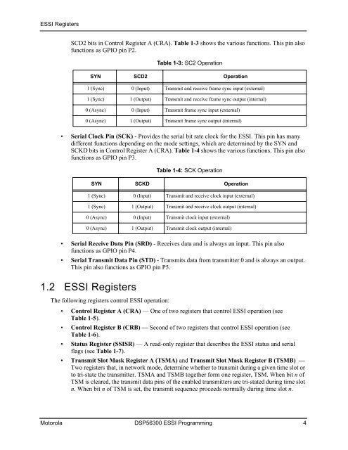
SCD2 bits in Control Register A (CRA). Table 1-3 shows the various functions. This pin also<br />
functions as GPIO pin P2.<br />
Serial Clock Pin (SCK) - Provides the serial bit rate clock for the <strong>ESSI</strong>. This pin has many<br />
different functions depending on the mode settings, which are determined by the SYN and<br />
SCKD bits in Control Register A (CRA). Table 1-4 shows the various functions. This pin also<br />
functions as GPIO pin P3.<br />
Serial Receive Data Pin (SRD) - Receives data and is always an input. This pin also<br />
functions as GPIO pin P4.<br />
Serial Transmit Data Pin (STD) - Transmits data from transmitter 0 and is always an output.<br />
This pin also functions as GPIO pin P5.<br />
1.2 <strong>ESSI</strong> Registers<br />
Table 1-3: SC2 Operation<br />
SYN SCD2 Operation<br />
1 (Sync) 0 (Input) Transmit and receive frame sync input (external)<br />
1 (Sync) 1 (Output) Transmit and receive frame sync output (internal)<br />
0 (Async) 0 (Input) Transmit frame sync input (external)<br />
0 (Async) 1 (Output) Transmit frame sync output (internal)<br />
Table 1-4: SCK Operation<br />
SYN SCKD Operation<br />
1 (Sync) 0 (Input) Transmit and receive clock input (external)<br />
1 (Sync) 1 (Output) Transmit and receive clock output (internal)<br />
0 (Async) 0 (Input) Transmit clock input (external)<br />
0 (Async) 1 (Output) Transmit clock output (internal)<br />
The following registers control <strong>ESSI</strong> operation:<br />
¥ Control Register A (CRA) Ñ One of two registers that control <strong>ESSI</strong> operation (see<br />
Table 1-5).<br />
¥ Control Register B (CRB) Ñ Second of two registers that control <strong>ESSI</strong> operation (see<br />
Table 1-6).<br />
¥ Status Register (SSISR) Ñ A read-only register that describes the <strong>ESSI</strong> status and serial<br />
flags (see Table 1-7).<br />
¥ Transmit Slot Mask Register A (TSMA) and Transmit Slot Mask Register B (TSMB) Ñ<br />
Two registers that, in network mode, determine whether to transmit during a given time slot or<br />
to tri-state the transmitter. TSMA and TSMB together form one register, TSM. When bit n of<br />
TSM is cleared, the transmit data pins of the enabled transmitters are tri-stated during time slot<br />
n.<br />
When bit n of TSM is set, the transmit sequence proceeds normally during time slot n.<br />
Motorola DSP56300 <strong>ESSI</strong> <strong>Programming</strong> 4