PhRC NEWSLETTER PHOTONICS'La - Nanyang Technological ...
PhRC NEWSLETTER PHOTONICS'La - Nanyang Technological ...
PhRC NEWSLETTER PHOTONICS'La - Nanyang Technological ...

Create successful ePaper yourself
Turn your PDF publications into a flip-book with our unique Google optimized e-Paper software.
Polymer Photonics<br />
Polymeric materials are broad and specific properties<br />
can be engineered for specific applications, including<br />
a wide bandwidth of transparency, high electrooptic<br />
(EO) coefficients, or high thermo-optic (TO) coefficients,<br />
making them suitable for very fast (picosecond)<br />
switches as well as low-power, millisecond switches and<br />
variable attenuators. Polymeric passive and active devices<br />
can be easily integrated on any surface of interest, and<br />
passive waveguides can be fabricated easily and at low cost<br />
with excellent control of refractive index and geometry.<br />
This makes polymer-based channel waveguides ideal for<br />
board-level chip-to-chip optical interconnects, and as interlayer<br />
dielectrics and protective overcoats.<br />
Research on polymer and polymer photonics has been<br />
Photonic Integrated Circuits Research<br />
A/P Chin Mee Koy<br />
Integrated optics, or photonic integrated circuits<br />
(PIC), began in Bell Labs over 40 years ago, but has<br />
only entered the industry lexicon in the last 10 years. This<br />
is because of its emerging importance as the surest way to<br />
reduce components cost, which forms a major portion<br />
of systems cost. Integration reduces the number of parts<br />
and hence the level of packaging and assembly required.<br />
It also results in parts with smaller footprints that save<br />
valuable space in central offices. Integrated components<br />
tend to be more reliable and power efficient and hence cut<br />
down operating cost. Because of these advantages, photonic<br />
integration is considered a key to opening the floodgate<br />
of low-cost optical subsystems that will make longterm<br />
sustainable investment in optical networks possible.<br />
Just as microelectronic integration has brought about the<br />
relentless reduction in the price of IC’s, photonic integration,<br />
likewise, can be expected to bring about similar<br />
benefits, and ultimately give the whole industry a path to<br />
long-term growth.<br />
The future networks are also migrating toward alloptical<br />
in order to eliminate the optical-electronic-optical<br />
(O-E-O) bottleneck. Based on this evolution, the next<br />
technology requirements are expected to be dominated<br />
by optical switching and routing functionality, with subsystems<br />
such as optical cross-connects (OXCs) and optical<br />
add/drop multiplexers (OADMs) as the lynchpin<br />
products. Many competing switching technologies are<br />
being developed, such as micro-electromechanical systems<br />
(MEMS), arrayed-waveguide gratings (AWG), liq-<br />
carried out jointly in the School of Materials Engineering<br />
and the School of Electrical and Electronic Engineering<br />
for a number of years. A niche area is highlighted below.<br />
Conjugated polymers are organic macromolecules with<br />
alternating single and double bonds along the molecular<br />
chains. The overlap of the pz orbitals gives rise to two<br />
molecular orbitals (HOMO, LUMO) that resemble the<br />
conduction and valence bands in semiconductors. So just<br />
like semiconductor materials, they can conduct electricity<br />
and in some cases, emit or absorb light. This makes<br />
them an interesting (and indeed fascinating) class of electronic<br />
materials to study. Conjugated polymers are strong<br />
candidates for flat panel displays. We have demonstrated<br />
organic LEDs (OLED) using both conjugated polymers<br />
and molecular complexes.<br />
uid crystals, fibre-based Mach-Zehnder, thin-films, and<br />
fibre Bragg gratings. However, all of these switches tend<br />
to be bulky and space-hungry and require complicated<br />
assembly and fibre management. Next-generation product<br />
development will need to drive down both cost and<br />
space. These requirements provide the motif for integration<br />
and favors technologies that are amenable to highdensity<br />
integration.<br />
Microphotonic integration is more challenging, and<br />
hence much less mature, than microelectronic integration.<br />
Partly this is due to the large diversity of photonic<br />
devices that need to be integrated. Unlike transistors<br />
which form the bedrock building block for all of electronics,<br />
no photonic equivalent of transistors exists.<br />
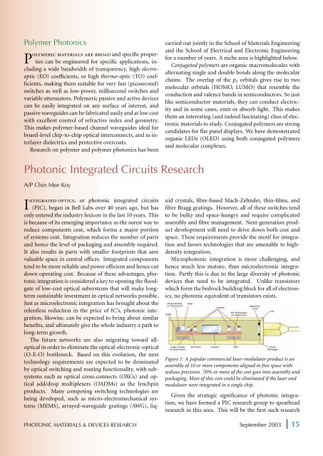
Figure 1: A popular commercial laser-modulator product is an<br />
assembly of 10 or more components aligned in free space with<br />
tedious precision. 70% or more of the cost goes into assembly and<br />
packaging. Most of this cost could be eliminated if the laser and<br />
modulator were integrated in a single chip.<br />
Given the strategic significance of photonic integration,<br />
we have formed a PIC research group to spearhead<br />
research in this area. This will be the first such research<br />
PHOTONIC MATERIALS & DEVICES RESEARCH September 2003 15