PhRC NEWSLETTER PHOTONICS'La - Nanyang Technological ...
PhRC NEWSLETTER PHOTONICS'La - Nanyang Technological ...
PhRC NEWSLETTER PHOTONICS'La - Nanyang Technological ...

You also want an ePaper? Increase the reach of your titles
YUMPU automatically turns print PDFs into web optimized ePapers that Google loves.
(b)<br />
Figure 1: (a) the selective area ICP-QWI process; and (b) SEM<br />
photograph of the extended-cavity laser. [1]<br />
Prof. Mei Ting’s group in <strong>PhRC</strong> has pioneered the<br />
research of plasma-based QWI technology and has<br />
obtained several promising preliminary results. Using<br />
Inductively Coupled Plasma (ICP) enhanced QWI,<br />
we have demonstrated large bandgap energy blueshifts<br />
(> 100 nm), selective area bandgap tuning and integration<br />
of laser and low-loss waveguide (with losses less than<br />
12.9 dBcm −1 ). Further study in ICP-QWI will be carried<br />
out as part of the larger program to develop PIC.<br />
Reference<br />
[1] H.S. Djie, et al, “Photonic Integration using Inductively<br />
Coupled Argon Plasma enhanced Quantum Well Intermixing”,<br />
Electron. Lett., vol. 38, no. 25, pp. 1672-1673,<br />
2002.<br />
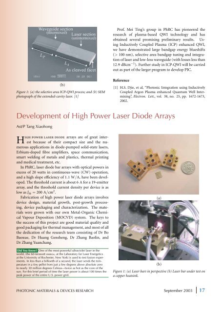
Development of High Power Laser Diode Arrays<br />
Ast/P Tang Xiaohong<br />
High power laser diode arrays are of great interest<br />
because of their compact size and the numerous<br />
applications in diode-pumped solid-state lasers,<br />
Erbium-doped fibre amplifiers, space communication,<br />
smart welding of metals and plastics, thermal printing<br />
and medical treatment, etc.<br />
In <strong>PhRC</strong>, laser diode bar arrays with optical powers in<br />
excess of 20 watts in continuous-wave (CW) operation,<br />
and a high slope efficiency of 1.1 W/A, have been developed.<br />
The threshold current is about 6 A for a 19-emitter<br />
array, and the threshold current density per device is as<br />
low as Jth = 200 A/cm2 .<br />
Fabrication of high power laser diode arrays involves<br />
device design, material growth, post-growth processing,<br />
device packaging and characterization. The materials<br />
were grown with our own Metal-Organic Chemical<br />
Vapour Deposition (MOCVD) system. The keys to<br />
the success of this project are good material quality and<br />
good packaging for thermal management, and most of all<br />
the dedication of the research team consisting of Dr Bo<br />
Baoxue, Dr Huang Gensheng, Dr Zhang Baolin, and<br />
Dr Zhang Yuanchang.<br />
Did You Know? One of the most powerful ultraviolet laser in the<br />
world, (the 60-terawatt omega, at the Laboratory for Laser Energetics<br />
at the University of Rochester, New York) is used to test fusion experiments.<br />
In less than a billionth of a second, the laser sends the temperature<br />
in a tiny pellet from just a few degrees above absolute zero<br />
to nearly 30 million degrees Celsius—twice as hot as the core of the<br />
sun. For this brief period of time the laser power is about 100 times the<br />
peak power of the entire U.S. power grid.<br />
(a)<br />
(b)<br />
Figure 1: (a) Laser bars in perspective (b) Laser bar under test on<br />
a copper heatsink.<br />
PHOTONIC MATERIALS & DEVICES RESEARCH September 2003 17