DDR4 Design Considerations - EEWeb
DDR4 Design Considerations - EEWeb
DDR4 Design Considerations - EEWeb

Create successful ePaper yourself
Turn your PDF publications into a flip-book with our unique Google optimized e-Paper software.
<strong>EEWeb</strong> PULSE TECH ARTICLE<br />
Click the image below to read Part 1:<br />
Continued from Part 1<br />
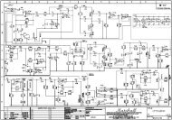
5. SYSTEM OVERVIEW<br />
After choosing the TDC structure, we started working<br />
on our design implementation following a top-down<br />
approach. From our point of view, and due to the large<br />
degree of freedom available for this design, this was the<br />
most logical starting point.<br />
5.1. Matrix structure<br />
Choosing an appropriate matrix structure was the first<br />
design issue we had to face. As already mentioned, there<br />
are two main considerations to take into account:<br />
• Dummy structure minimization within the matrix,<br />
since they consume power and contribute to the overall<br />
design area.<br />
• Delay stage loading since a homogeneous load for<br />
every delay stage will contribute to an easier design and<br />
a better resolution controllability.<br />
As discussed before, a bigger matrix yields a larger<br />
number of dummy structures but a more homogeneous<br />
capacitive load for both X and Y delay chains, as the<br />
row-column ratio approaches 1 and the matrix becomes<br />
square, making resolution easier to set. A smaller matrix<br />
will have the opposite effect, thus yielding a smaller<br />
number of dummy structures but making resolution harder<br />
to set.<br />
Keeping these two design parameters in mind, we<br />
derived the mathematical expressions for calculating<br />
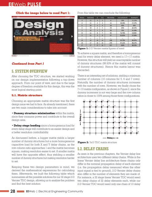
them. Afterwards, we built the following table which<br />
summarizes all the possible solutions for our 32 stage 2-D<br />
Vernier TDC design, allowing us to analyze the problem<br />
and find the best solution:<br />
From this table we can conclude the following: elements (X delay chain) and another one of 7 delay<br />
elements (Y delay chain).<br />
Figure 1: 2-D Vernier matrix figures of merit<br />
To achieve a square matrix, and therefore a homogeneous<br />
load for every delay element, we need a 17×17 matrix.<br />
However, this structure will yield an unacceptable number<br />
of dummy structures (88.93% of the matrix will consist<br />
of dummy structures). Hence this matrix layout was<br />
discarded.<br />
There is an interesting set of solutions, yielding a minimum<br />
number of columns (10 columns for 5, 6 and 7 rows).<br />
Naturally, the number of dummy structures increases<br />
with the number of rows. However, we finally chose the<br />
7×10 matrix configuration, as shown in Figure 2, since the<br />
dummy increment is not very large and the row-column<br />
ration is closer to 100% among those three configurations.<br />
Delay y<br />
1 8 15 22 29<br />
2 9 16 23 30<br />
3 10 17 24 31<br />
4 11 18 25 32<br />
5 12 19 26<br />
Delay x<br />
Figure 2: 7x10 TDC matrix structure<br />
5.2. DELAY CHAINS<br />
6 13 20 27<br />
7 14 21 28<br />
As seen in the previous chapters, the Vernier delay line<br />
architecture uses two different delay chains. While in the<br />
linear Vernier delay line architecture these chains only<br />
differ in the nominal propagation delay of each element<br />
(i.e. the propagation delay measured when the other<br />
input signal is tied to ground), 2-D Vernier delay chains<br />
also differ in the number of elements they are made of.<br />
For instance, a 32 stage linear Vernier TDC would need<br />
two delay chains of 32 delay elements each, while our<br />
2-D Vernier TDC would need only one chain of 10 delay<br />
For the delay stages within the chains, we decided to<br />
use non-inverting buffer structures as the main building<br />
blocks. These structures yield a worse propagation<br />
time than a single inverter, but they provide the delay<br />
comparison and encoding stages with a very simple<br />
time information format. For this purpose, we created<br />
two different components within our library, called BUF_X<br />
and BUF_Y.<br />
Since the Y delay chain has to be faster than the X delay<br />
chain but its capacitive load per delay element is, by<br />
construction, larger than the X’s, it makes sense to initially<br />
increase the size of the BUF_Y transistors. However, since<br />
we are only dealing with low-to-high transitions, this can<br />
be achieved by just increasing the pMOS transistor in<br />
the second inverter within the BUF_Y structure. For the<br />
BUF_X component we initially set to minimum size for<br />
both pMOS and nMOS transistors.<br />
Besides setting the minimum size, we added an extra<br />
delay element at the end of both delay chains. This final<br />
delay element was left open (actually it is driving a 1GΩ<br />
resistor to avoid Cadence WARNING messages) and<br />
its only goal is to balance every capacitive load within<br />
the chain.<br />
We also included an extra input delay stage on both chains,<br />
called FIX_DELAY within our library. These structures<br />
were used to provide a rise and fall time independent<br />
signals to the delay chain during the first design tests.<br />
While FIX_DELAY elements remained unchanged through<br />
the design process, BUF_X and BUF_Y buffers were<br />
resized and optimized to achieve the desired resolution.<br />
5.3. Delay comparators<br />
The time difference between the START and STOP signals<br />
is measured by the use of several memory elements<br />
which capture the moment when the START signal is<br />
surpassed by the STOP signal. Following this principle,<br />
a 32-bit pseudo thermo-code format is generated by<br />
the TDC, where the delay information is kept as the<br />
transition from 1 to 0. Finally, this code is passed to the<br />
5-bit encoding circuit.<br />
Choosing among all the available memory elements for<br />
this task, we followed the recommendations given in<br />
[1] and used a NAND gate based S-R latch as the basic<br />
delay comparison element. The main advantage which<br />
presents this structure is its symmetry for both S and<br />
R signals, helping us to achieve a more homogeneous<br />
capacitive loading for both the X and Y delay chains.<br />
Besides, we also included an inverting buffer at each<br />
output, as recommended in [1], making this device less<br />
sensitive to output loading variations and preventing the<br />
design from unwanted non-linear behavior.<br />
28 <strong>EEWeb</strong> | Electrical Engineering Community<br />
Visit www.eeweb.com<br />
S#<br />
R#<br />
Figure 3: Delay comparator (gate level)<br />
Figure 4: S-R latch truth table<br />
Q#<br />
Special care has to be taken when connecting the feedback<br />
and input signals to the NAND pull-down network due to<br />
data dependent delay. Indeed, the nominal propagation<br />
delay of each element within the chain can be affected<br />
by the S-R latch current state, introducing non-linear<br />
effects. In particular, for this TDC architecture, this effect<br />
becomes quite significant since there are several S-R<br />
latches connected to the same delay element output.<br />
Figure 5 shows the two possible configurations.<br />
VDD<br />
GND<br />
FB2<br />
FB2<br />
FB1<br />
S# R#<br />
FB1<br />
Config 1 Config 2<br />
FB1<br />
FB2<br />
VDD<br />
GND<br />
FB2<br />
FB2<br />
FB1<br />
S# R#<br />
Figure 5: Delay comparator (transistor level)<br />
We obtained some interesting results while testing both<br />
configurations; which are shown in Figure 6. In particular,<br />
this figure shows the propagation delay for each delay<br />
element within the X delay chain for both configurations.<br />
We used for this purpose a 10 ps resolution configuration<br />
and a time delay of 160 ps between the START and STOP<br />
FB1<br />
Q<br />
FB1<br />
FB2<br />
29