DDR4 Design Considerations - EEWeb
DDR4 Design Considerations - EEWeb
DDR4 Design Considerations - EEWeb

You also want an ePaper? Increase the reach of your titles
YUMPU automatically turns print PDFs into web optimized ePapers that Google loves.
<strong>EEWeb</strong> PULSE TECH ARTICLE<br />
signals. Therefore, the STOP signal will catch the START<br />
signal in the 16th delay comparator (2nd row, 3rd column).<br />
As can be seen, the propagation delay for the first<br />
configuration remains constant for the first and second<br />
columns, but it starts to decrease linearly after that due to<br />
a change in the capacitive load (data dependent delay).<br />
This is, of course, an undesired effect which must be<br />
avoided to prevent a non-linear behavior. On the other<br />
hand, by using the second configuration, each delay<br />
element within the X delay chain achieves a more uniform<br />
propagation delay and it’s almost data independent.<br />
Despite the fact that the use of this S-R latch configuration<br />
increases the nominal propagation delay, it is not a<br />
big issue and it can be readjusted by sizing the delay<br />
elements. Therefore we will be using the 2nd configuration<br />
in our SR_LATCH library component.<br />
Propagation Delay (ps)<br />
85<br />
83<br />
81<br />
79<br />
77<br />
75<br />
73<br />
71<br />
69<br />
67<br />
65<br />
Config 1<br />
Nom. Config 1 Config 2 Nom. Config 2<br />
X1-X2 X2-X3 X3-X4 X4-X5 X5-X6 X6-X7 X7-X8 X8-X9 X9-X10<br />
Delay Stage (X delay chain)<br />
Figure 6: Data dependent analysis for<br />
both configurations<br />
This concludes the basic description of our TDC delay<br />
comparator. However, as will be discussed in chapter 6,<br />
and due to the amount of dummy S-R latches introduced<br />
by the TDC matrix, we proceeded to substitute them for<br />
more optimal structures which roughly present the same<br />
capacitive loading, helping us to save area and power.<br />
Hence a new library component, called DUMMY, was<br />
created.<br />
5.4. Readout encoder<br />
Finally, we focused on the 32 to 5 encoder needed for the<br />
readout circuit. Since the existing/available testbench<br />
provided us with a quite good encoder, we decided to<br />
spend more effort into the matrix optimization.<br />
6. TUNING THE DESIGN<br />
Once the main design features have been described in<br />
the previous chapter, now we present all the different<br />
strategies we followed to achieve our current design.<br />
6.1. Area minimization<br />
Since our design was quite large in terms of the number<br />
of transistors, area minimization is a critical goal which<br />
allowed us to improve our design performance. In<br />
particular, we focused on the TDC matrix structure and<br />
devised several ways to improve its area consumption.<br />
6.1.1. Y chain load reduction<br />
We realized that for each row within the matrix, there are<br />
at most five out of ten useful devices for delay comparison.<br />
Hence, the Y delay chain had an excessive loading, which<br />
affected both the acquisition time and the circuit area for<br />
the same resolution.<br />
However, as we presented in the previous chapter, our<br />
S-R latch configuration made the circuit almost data<br />
independent. This feature allowed us to disconnect them<br />
from the Y chain and tie them to ground without harming<br />
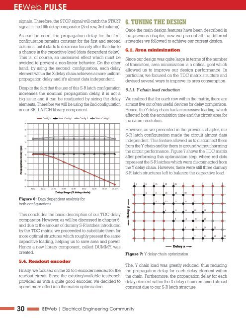
the circuit performance. Figure 7 shows the TDC matrix<br />
after performing this optimization step, where red dots<br />
represent the S-R latches which were disconnected from<br />
the Y delay chain. However, there were still three dummy<br />
S-R latch structures left to balance the capacitive load.<br />
Delay y<br />
1 8 15 22 29<br />
2 9 16 23 30<br />
3 10 17 24 31<br />
4 11 18 25 32<br />
5 12 19 26<br />
Delay x<br />
Figure 7: Y delay chain optimization<br />
6 13 20 27<br />
7 14 21 28<br />
The, Y chain load was greatly reduced, thus reducing<br />
the propagation delay for each delay element within<br />
the chain. Furthermore, the propagation delay for each<br />
delay element within the X delay chain remained almost<br />
constant due to our S-R latch structure.<br />
6.1.2. Dummy structures<br />
After the Y chain optimization, most of the S-R latches had<br />
one of their input tied to ground. Looking at their gate<br />
level schematic, it was easy to conclude the following:<br />
• Since one NAND gate had an input tied to ground, its<br />
output is tied to 1. This output is used as one of the inputs<br />
of the other NAND gate within the component.<br />
• Removing the former NAND gate along with its<br />
associated inverter reduced the circuit area maintaining a<br />
constant propagation delay for the X chain delay elements.<br />
• However, since these structures do not commute,<br />
dynamic power consumption was not affected by this<br />
optimization.<br />
With these ideas in mind, we obtained the following<br />
structure for our DUMMY component, which is basically<br />
a capacitive load:<br />
6.2. Resolution optimization<br />
As shown in section 3.2, our TDC resolution is given by<br />
the following relationships:<br />
30 <strong>EEWeb</strong> | Electrical Engineering Community<br />
Visit www.eeweb.com<br />
VDD<br />
R#<br />
GND<br />
1<br />
Figure 8: Dummy component (transistor level)<br />
1<br />
NOTE: A further area optimization can be easily done by<br />
removing one of the pMOS transistors within the NAND<br />
gate since it is always OFF. However we did not realize<br />
that until later, we could not include it in the submitted<br />
TDC design.<br />
6.1.3. S-R latch optimization<br />
Our final area improvement dealt with the active S-R<br />
latches themselves. As we only used one of the device<br />
outputs, we just removed the unused output, along with its<br />
associated inverter. By introducing this modification, we<br />
did not observe any major change in the delay element’s<br />
propagation delay.<br />
VDD<br />
GND<br />
S# R#<br />
Figure 9: Final S-R latch component (transistor level)<br />
The following table summarizes all the relevant parameters<br />
needed for a given resolution ranging from 5 to 10 ps:<br />
Figure 10: TDC resolution chart<br />
Therefore, by just sizing the delay elements within both<br />
delay chains we can achieve any required resolution.<br />
However, our TDC architecture presents two major<br />
drawbacks in comparison with the linear Vernier delay<br />
line architecture:<br />
• Our resolution is totally dependent on the propagation<br />
delay of each delay elements, as can be seen in the<br />
table above. Ignoring this fact will cause the system to<br />
behave in an unpredictable and highly non-linear way.<br />
Hence bigger delay elements will be needed if aiming<br />
for high resolution.<br />
• Each delay element has to drive a larger load, due to the<br />
matrix configuration. Again, sizing becomes a problem<br />
for a given resolution, limiting our design space.<br />
Due to this, we aimed for a 9 ps resolution, which is<br />
slightly better than the proposed in the midterm report<br />
and does not imply too large transistors.<br />
Q<br />
31