615611 Electronics Workshop 2 Manual - Thames & Kosmos
615611 Electronics Workshop 2 Manual - Thames & Kosmos
615611 Electronics Workshop 2 Manual - Thames & Kosmos

Create successful ePaper yourself
Turn your PDF publications into a flip-book with our unique Google optimized e-Paper software.
V<br />
R<br />
T<br />
nd and N N<br />
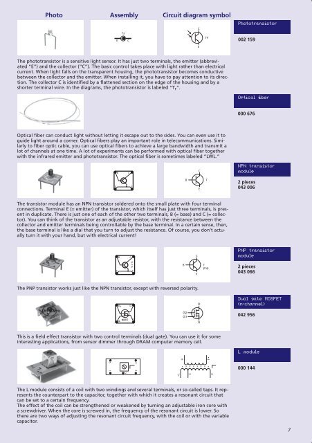
The phototransistor + + is a sensitive light sensor . It DGe<br />
DGe has just two terminals, the emitter + + (abbrevi-<br />
C<br />
ated “E”) and C<br />
A K<br />
the collector (“C”) . The basic control takes place with light rather than A D<br />
AMP A AMP electrical<br />
–<br />
Ge<br />
current . When light falls on the transparent housing, the phototransistor becomes – conductive<br />
E E<br />
between the collector and the emitter . When installing it, you have to pay attention K to its direction<br />
. The collector A A C is identified by a flattened section on the edge of the housing and by a<br />
D DE EFF shorter terminal wire . In the diagrams, the phototransistor is labeled “TF” .<br />
DD<br />
P P<br />
Ge Ge<br />
EP<br />
EP EP<br />
K K<br />
Optical fiber can conduct light without letting it Cescape<br />
C out to the sides . You can even use it to<br />
C C<br />
guide light around a corner . Optical fibers play an important role in telecommunications . Simi-<br />
LED 1<br />
A A<br />
A<br />
larly to fiber optic cable, you can use optical fibers DSi DSi to achieve a large bandwidth and transmit a<br />
AA A K KK<br />
DD<br />
lot of channels at one time . A lot of experiments can be performed with optical fiber together<br />
Ta Ta<br />
Si Si<br />
with the infrared emitter and phototransistor . LED The LED 2 optical fiber is sometimes labeled LED “LWL .”<br />
A A<br />
LED LED<br />
K K<br />
C C<br />
C C<br />
SP SP<br />
C C<br />
Potentiometer terminal wires connected<br />
ent in duplicate E E . There is just one of each<br />
to<br />
Double of the<br />
to contact<br />
variable other<br />
contact clips G,<br />
capacitor two terminals, B (= base) and C (= collec-<br />
G, H, H, and and I I<br />
B HS HS<br />
tor) . You can think of the transistor as an connected adjustable to clips A, resistor, B, and C<br />
TF TF<br />
with the resistance between the<br />
collector A Aand emitter C C terminals being controllable EP EP by the base terminal . In a certain sense, then,<br />
the base terminal E Eis<br />
like a dial that you turn to LED LED 3adjust<br />
3 the resistance . Of course, EP you EP A A don’t actually<br />
turn it with your A hand, but with electrical current!<br />
DSi<br />
A A K K<br />
A K V VB<br />
B<br />
D<br />
LED<br />
+<br />
A K<br />
LED<br />
+ Si<br />
A K<br />
A A<br />
IR-LED IR-LED<br />
K K<br />
AMP<br />
– – K<br />
+<br />
C C<br />
LED 1<br />
B B C C<br />
E E<br />
324<br />
Ta Ta<br />
–<br />
p p<br />
A K<br />
n n<br />
p p<br />
B B T T<br />
pnp pnp LED 2<br />
E E LED LED 1 1E<br />
E<br />
A A<br />
P P<br />
E E<br />
A K<br />
A A K K<br />
OP<br />
A<br />
DSi<br />
A K<br />
D<br />
Si<br />
K<br />
+<br />
324<br />
– OP<br />
onnected nected<br />
F<br />
onnected nected<br />
d I<br />
1<br />
6<br />
2<br />
R R<br />
C<br />
+ 5V + 5V D1 D1<br />
C<br />
Photo Speaker Assembly terminal wires Circuit diagram SP SP symbol<br />
connected D2 to to contact D2 clips M and and NN<br />
4<br />
3<br />
AMP<br />
AMP<br />
E<br />
E<br />
–<br />
–<br />
E E CC<br />
Potentiometer terminal wires connected<br />
to to contact clips D, D, E, E, and and F<br />
R R<br />
F<br />
Ta<br />
This is a field effect Si Si transistor with two control terminals (dual gate) . You can use it for some<br />
interesting applications, from sensor dimmer through 555 DRAM 555<br />
– – + +<br />
computer memory cell .<br />
TF C CTF<br />
A<br />
A<br />
V<br />
V<br />
+<br />
+<br />
X XDGe<br />
DGe<br />
A A K K<br />
G GH HII A – B – C<br />
Potentiometer terminal wires connected<br />
V V<br />
C C<br />
E E<br />
K K<br />
K<br />
+ +<br />
C C<br />
C<br />
The transistor module has an NPN transistor soldered onto the small plate with four terminal<br />
BB T T<br />
K K<br />
connections . Terminal E (= emitter) of the transistor, which itself has just three terminals, is pres-<br />
6<br />
1<br />
+<br />
A C K KC<br />
B C<br />
E + +<br />
E<br />
2<br />
–<br />
4 3<br />
1<br />
6<br />
EP<br />
A<br />
+<br />
TF TF<br />
C<br />
Ta<br />
B T<br />
+ A+<br />
A<br />
E<br />
x HS x HS<br />
D D<br />
– –<br />
A Ge C CGe<br />
4024 LED LED 2 2 4024<br />
+ +<br />
The R PNP transistor R works Rjust<br />
like the R NPN transistor, 324 324except<br />
with reversed polarity OP OP.<br />
+<br />
C<br />
C<br />
–<br />
A A<br />
KC<br />
K<br />
D D<br />
1<br />
4<br />
1<br />
1 2<br />
5<br />
2<br />
2 3<br />
6<br />
3<br />
3 4<br />
7<br />
4<br />
4 5<br />
5<br />
5 6<br />
6<br />
6 7<br />
7<br />
7<br />
14<br />
11<br />
14<br />
14 13<br />
10<br />
13<br />
13 12<br />
9<br />
12<br />
12 11<br />
8<br />
11<br />
11 10<br />
10<br />
10 9<br />
9<br />
9 8<br />
8<br />
8<br />
IN<br />
IN<br />
PCO<br />
PCO<br />
+<br />
+<br />
– –<br />
OUT<br />
OUT<br />
VCO<br />
VCO<br />
G GH HI I<br />
+ 9V<br />
+ 9V<br />
E<br />
E OUT 1<br />
COUT<br />
1<br />
C<br />
E<br />
E OUT 2<br />
COUT<br />
2<br />
C<br />
IN 1<br />
IN 1 2<br />
IN 32<br />
IN 43<br />
IN 4<br />
0V<br />
0V<br />
– 9V<br />
– 9V<br />
2<br />
+<br />
PCO + IN<br />
PCO IN<br />
P P<br />
4<br />
Solar Solar<br />
B B<br />
MM<br />
IN IN<br />
3<br />
VCO OUT<br />
VCO OUT<br />
PLL<br />
R PLLVCI<br />
R – VCI<br />
–<br />
NTC NTC<br />
there are two ways of adjusting the resonant circuit frequency, with the coil or with NTC NTC the variable<br />
HS HS<br />
PLL<br />
PLL<br />
The L module consists of a coil with two windings and several terminals, or so-called taps . It represents<br />
the counterpart to the capacitor, together with which it creates a resonant circuit that<br />
can be set to a certain frequency .<br />
The effect of the coil can be strengthened or weakened by turning an adjustable iron core with<br />
a screwdriver . When the core is screwed in, the frequency of the resonant circuit is lower . So<br />
capacitor .<br />
+<br />
C<br />
–<br />
GND<br />
+<br />
C<br />
C<br />
GNDD3<br />
Dig<br />
C<br />
7<br />
8<br />
6<br />
9<br />
K1<br />
OUT<br />
555<br />
6<br />
6<br />
1<br />
1<br />
+<br />
+<br />
5<br />
10<br />
– +<br />
CTRL R<br />
–<br />
–<br />
+<br />
+<br />
K2 DIS<br />
–<br />
K2 DIS<br />
555<br />
K1 OUT<br />
D3<br />
Dig<br />
Ta<br />
Ta<br />
–<br />
A A K K<br />
B B C C<br />
G2D A AB BCC 2<br />
2<br />
–<br />
4<br />
1<br />
5<br />
2<br />
6<br />
3<br />
7<br />
4<br />
11<br />
14<br />
10<br />
13<br />
9<br />
12<br />
8<br />
11<br />
–<br />
–<br />
VCI<br />
VCI<br />
R<br />
R<br />
4 3<br />
4 3<br />
3<br />
12<br />
3<br />
G2D E E E E<br />
G1<br />
S MOSFET<br />
G1<br />
MOSFET<br />
+<br />
C<br />
Double variable capacitor<br />
connected to to clips clips A, A, B, B, and and C C<br />
+ +<br />
G H I<br />
G H I<br />
K1 OUT<br />
CTRL R –<br />
–<br />
R<br />
2<br />
P<br />
CLK<br />
1<br />
4024 +<br />
1<br />
1<br />
R R<br />
LED LED<br />
K K<br />
– –<br />
14<br />
Q1<br />
Q2<br />
Q3<br />
Q4<br />
Q5<br />
Q6<br />
14<br />
Q7<br />
– Q1<br />
7<br />
Q2<br />
Q3<br />
Q4<br />
Q5<br />
Q6<br />
Q7<br />
–<br />
7<br />
6<br />
14<br />
5<br />
4<br />
13<br />
3<br />
12<br />
S<br />
2<br />
13<br />
G2<br />
G1<br />
1<br />
14<br />
1<br />
9<br />
3<br />
12<br />
11<br />
D<br />
S<br />
2<br />
R<br />
4<br />
K1 OUT<br />
+<br />
–<br />
CTRL R<br />
555<br />
K2 DIS<br />
– +<br />
C C<br />
E E<br />
D<br />
B B<br />
G2<br />
T T<br />
G1<br />
E E<br />
S<br />
6<br />
6<br />
5<br />
P<br />
A A C C<br />
K2<br />
DIS<br />
2<br />
2<br />
555<br />
CLK<br />
1<br />
4024 +<br />
6<br />
9<br />
12<br />
11<br />
CTRL<br />
R<br />
+<br />
4<br />
4<br />
3<br />
3<br />
Ta<br />
B C<br />
Phototransistor<br />
002 159<br />
Optical fiber<br />
324 324<br />
000 676<br />
+ 9V<br />
+ 9V<br />
– –<br />
Potentiometer terminal wires connected<br />
D DE EFF to contact clips G, H, and I<br />
G GHHII Dual gate MOSFET<br />
E<br />
(n-channel)<br />
042 956<br />
LED LED 3 3<br />
AA KK<br />
D E F<br />
AA KK<br />
IR-LED<br />
B B C C<br />
Potentiometer terminal wires connected<br />
p p<br />
to contact n clips n D, E, and F<br />
p p<br />
E E E E<br />
1<br />
1<br />
2<br />
2<br />
3<br />
3<br />
4<br />
4<br />
5<br />
5<br />
6<br />
6<br />
7<br />
7<br />
14<br />
14<br />
13<br />
13<br />
12<br />
12<br />
11<br />
11<br />
10<br />
10<br />
9<br />
9<br />
8<br />
8<br />
IN<br />
IN<br />
PCO<br />
PCO<br />
+<br />
+<br />
+ +<br />
E<br />
E OUT 1<br />
COUT<br />
1<br />
C<br />
E<br />
E OUT 2<br />
COUT<br />
2<br />
C<br />
+ + HS HS<br />
X X TF<br />
TF<br />
– – E C<br />
OUT<br />
OUT<br />
PLL<br />
PLL<br />
VCO<br />
VCO<br />
NPN transistor<br />
module<br />
2 pieces<br />
043 006<br />
Ta<br />
AMP<br />
E<br />
–<br />
E<br />
E<br />
+<br />
+<br />
1–IN<br />
1–IN<br />
NTC NTC<br />
A<br />
–<br />
–<br />
G H I<br />
VCI<br />
VCI<br />
R<br />
R<br />
IN 2<br />
IN 2<br />
IN 3<br />
IN 3<br />
IN 4<br />
IN 4<br />
0V<br />
0V<br />
– 9V<br />
– 9V<br />
7<br />
V<br />
+<br />
Speaker DSi<br />
DSi terminal wires<br />
connected A to to contact clips K Kclips<br />
M M and and N N<br />
PNP transistor<br />
module LED 1<br />
A<br />
A K<br />
2 pieces<br />
LED 2<br />
043 066<br />
A K<br />
B C<br />
E E<br />
L module<br />
000 144<br />
AMP<br />
AMP<br />
–<br />
–<br />
M MN N<br />
TF TF<br />
E E C C<br />
A<br />
A<br />
V<br />
V<br />
+<br />
+<br />
Potentiometer terminal wires wires connected<br />
to to contact clips clips D, D, E, E, and and F F<br />
Ta<br />
DSi DSi<br />
A A K K<br />
A<br />
LED<br />
K<br />
C<br />
B T B T<br />
G GH HI I<br />
Potentiometer terminal wires wires connected<br />
to to contact clips clips G, G, H, H, and and I I<br />
Ta<br />
LED<br />
K<br />
C<br />
E