Xilinx Using Block RAM in Spartan-3 FPGAs application note ...
Xilinx Using Block RAM in Spartan-3 FPGAs application note ...
Xilinx Using Block RAM in Spartan-3 FPGAs application note ...

Create successful ePaper yourself
Turn your PDF publications into a flip-book with our unique Google optimized e-Paper software.
XAPP463 (v1.1.2) July 23, 2003<br />
R<br />
Application Note: <strong>Spartan</strong>-3 FPGA Family<br />
<strong>Us<strong>in</strong>g</strong> <strong>Block</strong> <strong>RAM</strong> <strong>in</strong> <strong>Spartan</strong>-3 <strong>FPGAs</strong><br />
Summary For <strong>application</strong>s requir<strong>in</strong>g large, on-chip memories, <strong>Spartan</strong>-3 <strong>FPGAs</strong> provides plentiful,<br />
efficient Select<strong>RAM</strong> memory blocks. <strong>Us<strong>in</strong>g</strong> various configuration options, Select<strong>RAM</strong> blocks<br />
create <strong>RAM</strong>, ROM, FIFOs, large look-up tables, data width converters, circular buffers, and shift<br />
registers, each support<strong>in</strong>g various data widths and depths. This <strong>application</strong> <strong>note</strong> describes the<br />
features and capabilities of block Select<strong>RAM</strong> and illustrates how to specify the various options<br />
us<strong>in</strong>g the <strong>Xil<strong>in</strong>x</strong> CORE Generator system or via VHDL or Verilog <strong>in</strong>stantiation. Various nonobvious<br />
block <strong>RAM</strong> <strong>application</strong>s are discussed with references to additional tools, <strong>application</strong><br />
<strong>note</strong>s, and documentation.<br />
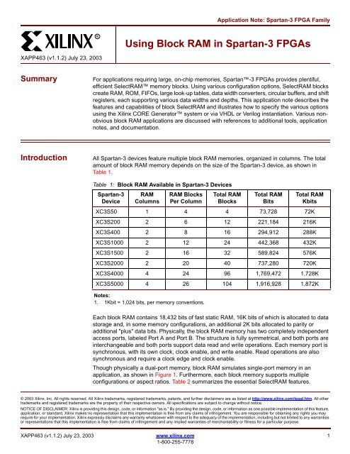
Introduction All <strong>Spartan</strong>-3 devices feature multiple block <strong>RAM</strong> memories, organized <strong>in</strong> columns. The total<br />
amount of block <strong>RAM</strong> memory depends on the size of the <strong>Spartan</strong>-3 device, as shown <strong>in</strong><br />
Table 1.<br />
Table 1: <strong>Block</strong> <strong>RAM</strong> Available <strong>in</strong> <strong>Spartan</strong>-3 Devices<br />
<strong>Spartan</strong>-3<br />
Device<br />
<strong>RAM</strong><br />
Columns<br />
<strong>RAM</strong> <strong>Block</strong>s<br />
Per Column<br />
Total <strong>RAM</strong><br />
<strong>Block</strong>s<br />
Total <strong>RAM</strong><br />
Bits<br />
Total <strong>RAM</strong><br />
Kbits<br />
XC3S50 1 4 4 73,728 72K<br />
XC3S200 2 6 12 221,184 216K<br />
XC3S400 2 8 16 294,912 288K<br />
XC3S1000 2 12 24 442,368 432K<br />
XC3S1500 2 16 32 589,824 576K<br />
XC3S2000 2 20 40 737,280 720K<br />
XC3S4000 4 24 96 1,769,472 1,728K<br />
XC3S5000 4 26 104 1,916,928 1,872K<br />
Notes:<br />
1. 1Kbit = 1,024 bits, per memory conventions.<br />
Each block <strong>RAM</strong> conta<strong>in</strong>s 18,432 bits of fast static <strong>RAM</strong>, 16K bits of which is allocated to data<br />
storage and, <strong>in</strong> some memory configurations, an additional 2K bits allocated to parity or<br />
additional "plus" data bits. Physically, the block <strong>RAM</strong> memory has two completely <strong>in</strong>dependent<br />
access ports, labeled Port A and Port B. The structure is fully symmetrical, and both ports are<br />
<strong>in</strong>terchangeable and both ports support data read and write operations. Each memory port is<br />
synchronous, with its own clock, clock enable, and write enable. Read operations are also<br />
synchronous and require a clock edge and clock enable.<br />
Though physically a dual-port memory, block <strong>RAM</strong> simulates s<strong>in</strong>gle-port memory <strong>in</strong> an<br />
<strong>application</strong>, as shown <strong>in</strong> Figure 1. Furthermore, each block memory supports multiple<br />
configurations or aspect ratios. Table 2 summarizes the essential Select<strong>RAM</strong> features.<br />
© 2003 <strong>Xil<strong>in</strong>x</strong>, Inc. All rights reserved. All <strong>Xil<strong>in</strong>x</strong> trademarks, registered trademarks, patents, and further disclaimers are as listed at http://www.xil<strong>in</strong>x.com/legal.htm. All other<br />
trademarks and registered trademarks are the property of their respective owners. All specifications are subject to change without notice.<br />
NOTICE OF DISCLAIMER: <strong>Xil<strong>in</strong>x</strong> is provid<strong>in</strong>g this design, code, or <strong>in</strong>formation "as is." By provid<strong>in</strong>g the design, code, or <strong>in</strong>formation as one possible implementation of this feature,<br />
<strong>application</strong>, or standard, <strong>Xil<strong>in</strong>x</strong> makes no representation that this implementation is free from any claims of <strong>in</strong>fr<strong>in</strong>gement. You are responsible for obta<strong>in</strong><strong>in</strong>g any rights you may<br />
require for your implementation. <strong>Xil<strong>in</strong>x</strong> expressly disclaims any warranty whatsoever with respect to the adequacy of the implementation, <strong>in</strong>clud<strong>in</strong>g but not limited to any warranties<br />
or representations that this implementation is free from claims of <strong>in</strong>fr<strong>in</strong>gement and any implied warranties of merchantability or fitness for a particular purpose.<br />
XAPP463 (v1.1.2) July 23, 2003 www.xil<strong>in</strong>x.com 1<br />
1-800-255-7778
R<br />
WEA<br />
ENA<br />
SSRA<br />
CLKA<br />
ADDRA[r A–1:0]<br />
DIA[w A–1:0]<br />
DIPA[3:0]<br />
WEB<br />
ENB<br />
SSRB<br />
CLKB<br />
ADDRB[r B–1:0]<br />
DIB[w B–1:0]<br />
DIPB[3:0]<br />
<strong>Us<strong>in</strong>g</strong> <strong>Block</strong> <strong>RAM</strong> <strong>in</strong> <strong>Spartan</strong>-3 <strong>FPGAs</strong><br />
Cascade multiple block <strong>RAM</strong>s to create deeper and wider memory organizations, with a<br />
m<strong>in</strong>imal tim<strong>in</strong>g penalty <strong>in</strong>curred through specialized rout<strong>in</strong>g resources.<br />
<strong>RAM</strong>16_w A_w B<br />
DOPA[pA–1:0] DOA[wA–1:0] DOPB[pB–1:0] DOB[wB–1:0] WE<br />
EN<br />
SSR<br />
CLK<br />
ADDR[r–1:0]<br />
DI[w–1:0]<br />
DIP[p–1:0]<br />
<strong>RAM</strong>16_Sw<br />
(a) Dual-Port (b) S<strong>in</strong>gle-Port<br />
Figure 1: Select<strong>RAM</strong> 18K <strong>Block</strong>s Perform as Dual-Port (a) and S<strong>in</strong>gle-Port (b) Memory<br />
DOP[p–1:0]<br />
DO[w–1:0]<br />
X463_01_040403<br />
Notes:<br />
1. w A and w B are <strong>in</strong>tegers represent<strong>in</strong>g the total data path width (i.e., data bits plus parity bits) at ports A and B, respectively.<br />
2. p A and p B are <strong>in</strong>tegers that <strong>in</strong>dicate the number of data path l<strong>in</strong>es serv<strong>in</strong>g as parity bits.<br />
3. r A and r B are <strong>in</strong>tegers represent<strong>in</strong>g the address bus width at ports A and B, respectively.<br />
4. The control signals CLK, WE, EN, and SSR on both ports have the option of <strong>in</strong>verted polarity.<br />
Table 2: Select<strong>RAM</strong> 18K <strong>Block</strong> Memory Features and Applications<br />
Total <strong>RAM</strong> bits, <strong>in</strong>clud<strong>in</strong>g parity 18,432 (16K data + 2K parity)<br />
Memory Organizations 16Kx1<br />
8Kx2<br />
4Kx4<br />
2Kx8 (no parity)<br />
2Kx9 (x8 + parity)<br />
1Kx16 (no parity)<br />
1Kx18 (x16 + 2 parity)<br />
512x32 (no parity)<br />
512x36 (x32 + 4 parity)<br />
256x72 (s<strong>in</strong>gle-port only)<br />
Parity Available and optional only for organizations greater than<br />
byte-wide. Parity bits optionally available as extra data<br />
bits.<br />
Performance 200 MHz (estimated)<br />
2 www.xil<strong>in</strong>x.com XAPP463 (v1.1.2) July 23, 2003<br />
1-800-255-7778
<strong>Us<strong>in</strong>g</strong> <strong>Block</strong> <strong>RAM</strong> <strong>in</strong> <strong>Spartan</strong>-3 <strong>FPGAs</strong><br />
<strong>Block</strong> <strong>RAM</strong><br />
Location and<br />
Surround<strong>in</strong>g<br />
Neighborhood<br />
Table 2: Select<strong>RAM</strong> 18K <strong>Block</strong> Memory Features and Applications (Cont<strong>in</strong>ued)<br />
Tim<strong>in</strong>g Interface Simple synchronous <strong>in</strong>terface. Similar to read<strong>in</strong>g and<br />
writ<strong>in</strong>g from a register with a setup time for write<br />
operations and clock-to-output delay for read operations.<br />
S<strong>in</strong>gle-Port Yes<br />
True Dual-Port Yes<br />
ROM, Initial <strong>RAM</strong> Contents Yes<br />
Mixed Data Port Widths Yes<br />
Power-Up Condition User-def<strong>in</strong>ed data, defaults to zero<br />
Potential Applications Local data storage, FIFOs, elastic stores, register files,<br />
buffers, stacks, circular buffers, shift registers, delay<br />
l<strong>in</strong>es, waveform storage and generation, direct digital<br />
synthesis, CAMs, associative memories, function tables,<br />
function generators, wide logic functions, code<br />
converters, encoders, decoders, counters, state<br />
mach<strong>in</strong>es, microsequencers, program storage for<br />
embedded processor(s)<br />
The <strong>Xil<strong>in</strong>x</strong> CORE Generator system supports various modules conta<strong>in</strong><strong>in</strong>g block <strong>RAM</strong> for<br />
<strong>Spartan</strong>-3 devices <strong>in</strong>clud<strong>in</strong>g:<br />
Embedded dual- or s<strong>in</strong>gle-port <strong>RAM</strong> modules<br />
ROM modules<br />
Synchronous and asynchronous FIFO modules<br />
Content-Addressable Memory (CAM) modules<br />
Furthermore, block <strong>RAM</strong> can be <strong>in</strong>stantiated <strong>in</strong> any synthesis-based design us<strong>in</strong>g the<br />
appropriate “<strong>RAM</strong>B16” module from the <strong>Xil<strong>in</strong>x</strong> design library.<br />
This <strong>application</strong> <strong>note</strong> describes the signals and attributes of the <strong>Spartan</strong>-3 block <strong>RAM</strong> feature,<br />
<strong>in</strong>clud<strong>in</strong>g details on the various attributes and <strong>application</strong>s for block <strong>RAM</strong>.<br />
As mentioned previously, block <strong>RAM</strong> is organized <strong>in</strong> columns. Figure 2 shows the <strong>Block</strong> <strong>RAM</strong><br />
column arrangement for the XC3S200. The XC3S50 has a s<strong>in</strong>gle column of block <strong>RAM</strong>, located<br />
two CLB columns from the left edge of the device. <strong>Spartan</strong>-3 devices larger than the XC3S50<br />
have two columns of block <strong>RAM</strong>, adjacent to the left and right edges of the die, located two<br />
columns of CLBs from the I/Os at the edge. In addition to the block <strong>RAM</strong> columns at the edge,<br />
the XC3S4000 and XC3S5000 have two additional columns—a total of four columns—nearly<br />
equally distributed between the two edge columns. Table 1 describes the number of columns<br />
and the total amount of block <strong>RAM</strong> on a specific device. The edge columns make block <strong>RAM</strong><br />
particularly useful <strong>in</strong> buffer<strong>in</strong>g or resynchroniz<strong>in</strong>g buses enter<strong>in</strong>g or leav<strong>in</strong>g the <strong>Spartan</strong>-3<br />
device.<br />
XAPP463 (v1.1.2) July 23, 2003 www.xil<strong>in</strong>x.com 3<br />
1-800-255-7778<br />
R
R<br />
XC3S200<br />
XC3S400<br />
XC3S1000<br />
XC3S1500<br />
XC3S2000<br />
<strong>Block</strong> <strong>RAM</strong> Columns<br />
<strong>Us<strong>in</strong>g</strong> <strong>Block</strong> <strong>RAM</strong> <strong>in</strong> <strong>Spartan</strong>-3 <strong>FPGAs</strong><br />
XC3S50<br />
XC3S4000<br />
XC3S5000<br />
2 CLBs<br />
Embedded Multipliers<br />
2 CLBs<br />
Figure 2: <strong>Block</strong> <strong>RAM</strong>s Arranged <strong>in</strong> Columns with Detailed Floorplan of XC3S200<br />
X463_02_062503<br />
Immediately adjacent to each block <strong>RAM</strong> is an embedded 18x18 hardware multiplier. Colocat<strong>in</strong>g<br />
block <strong>RAM</strong> and the embedded multipliers improves the performance of some digital<br />
signal process<strong>in</strong>g functions.<br />
Special <strong>in</strong>terconnect surround<strong>in</strong>g the block <strong>RAM</strong> provides efficient signal distribution for<br />
address and data. Furthermore, special provisions allow multiple block <strong>RAM</strong>s to be cascaded<br />
to create wider or deeper memories.<br />
Data Flows <strong>Spartan</strong>-3 block <strong>RAM</strong> is constructed of true dual-port memory and simultaneously supports all<br />
the data flows and operations shown <strong>in</strong> Figure 3. Both ports access the same set of memory<br />
bits but with two potentially different address schemes depend<strong>in</strong>g on the port’s data width.<br />
1. Port A behaves as an <strong>in</strong>dependent s<strong>in</strong>gle-port <strong>RAM</strong> support<strong>in</strong>g simultaneous read and<br />
write operations us<strong>in</strong>g a s<strong>in</strong>gle set of address l<strong>in</strong>es.<br />
2. Port B behaves as an <strong>in</strong>dependent s<strong>in</strong>gle-port <strong>RAM</strong> support<strong>in</strong>g simultaneous read and<br />
write operations us<strong>in</strong>g a s<strong>in</strong>gle set of address l<strong>in</strong>es.<br />
3. Port A is the write port with a separate write address and Port B is the read port with a<br />
separate read address. The data widths for Port A and Port B can be different also.<br />
4. Port B is the write port with a separate write address and Port A is the read port with a<br />
separate read address. The data widths for Port B and Port A can be different also.<br />
4 www.xil<strong>in</strong>x.com XAPP463 (v1.1.2) July 23, 2003<br />
1-800-255-7778
<strong>Us<strong>in</strong>g</strong> <strong>Block</strong> <strong>RAM</strong> <strong>in</strong> <strong>Spartan</strong>-3 <strong>FPGAs</strong><br />
Write<br />
Read<br />
Write<br />
1<br />
Read<br />
Figure 3: <strong>Block</strong> <strong>RAM</strong> Support S<strong>in</strong>gle- and Dual-Port Data Transfers<br />
Signals The signals connected to a block <strong>RAM</strong> primitive divide <strong>in</strong>to four categories, as listed below.<br />
Table 3 lists the block <strong>RAM</strong> <strong>in</strong>terface signals, the signals names for both s<strong>in</strong>gle-port and dualport<br />
memories, and signal direction.<br />
1. Data Inputs and Outputs<br />
2. Parity Inputs and Outputs, available when a data port is byte-wide or wider<br />
3. Address <strong>in</strong>puts to select a specific memory location<br />
4. Various control signals that manage read, write, or set/reset operations.<br />
Data Inputs and Outputs<br />
4<br />
<strong>Spartan</strong>-3<br />
Dual Port<br />
<strong>Block</strong> <strong>RAM</strong><br />
Read 3<br />
Write<br />
2<br />
Read<br />
X463_03_020503<br />
The total width of a port’s data port <strong>in</strong>cludes both the data bus and the parity bus, when<br />
applicable, as shown <strong>in</strong> Figure 4. In the 512x36 organization, for example, the 36-bit data port<br />
width <strong>in</strong>cludes four parity bits as the more significant bits followed by the 32 data bits as the less<br />
significant bits.<br />
The data and parity <strong>in</strong>put and output signals are always buses; that is, <strong>in</strong> a 1-bit width<br />
configuration, the data <strong>in</strong>put signal is DI[0] and the data output signal is DO[0].<br />
XAPP463 (v1.1.2) July 23, 2003 www.xil<strong>in</strong>x.com 5<br />
1-800-255-7778<br />
Port A<br />
Table 3: <strong>Block</strong> <strong>RAM</strong> Interface Signals<br />
Port B<br />
Write<br />
Dual Port<br />
Signal Description S<strong>in</strong>gle Port Port A Port B Direction<br />
Data Input Bus DI DIA DIB Input<br />
Parity Data Input Bus (available only for<br />
byte-wide and wider organizations)<br />
DIP DIPA DIPB Input<br />
Data Output Bus DO DOA DOB Output<br />
Parity Data Output (available only for<br />
byte-wide and wider organizations)<br />
DOP DOPA DOPB Output<br />
Address Bus ADDR ADDRA ADDRB Input<br />
Write Enable WE WEA WEB Input<br />
Clock Enable EN ENA ENB Input<br />
Synchronous Set/Reset SSR SSRA SSRB Input<br />
Clock CLK CLKA CLKB Input<br />
R
R<br />
512x36<br />
<strong>Us<strong>in</strong>g</strong> <strong>Block</strong> <strong>RAM</strong> <strong>in</strong> <strong>Spartan</strong>-3 <strong>FPGAs</strong><br />
Data Input Bus — DI[#:0] (DIA[#:0], DIB[#:0])<br />
The Data Input bus is the source of data to be written <strong>in</strong>to <strong>RAM</strong>.<br />
Data at the DI <strong>in</strong>put bus is written to the <strong>RAM</strong> location specified by the address <strong>in</strong>put bus,<br />
ADDR, dur<strong>in</strong>g a Low-to-High transition on the CLK <strong>in</strong>put, when the clock enable EN and write<br />
enable WE <strong>in</strong>puts are High.<br />
Parity Data<br />
35 34 33 32 31 24 23 16 15 8 7<br />
P3 P2 P1 P0<br />
Byte 3<br />
1Kx18<br />
Parity Optional<br />
(16Kbits data,<br />
2Kbits parity)<br />
Byte 2<br />
Figure 4: Data Organization and Mapp<strong>in</strong>g Between Modes<br />
6 www.xil<strong>in</strong>x.com XAPP463 (v1.1.2) July 23, 2003<br />
1-800-255-7778<br />
Byte 1<br />
17 16 15<br />
8<br />
P3 P2<br />
P1 P0<br />
Byte 3<br />
Byte 1<br />
2Kx9<br />
8<br />
P3<br />
P2<br />
P1<br />
P0<br />
No Parity<br />
(16Kbits data)<br />
7<br />
7<br />
4Kx4<br />
Byte 0<br />
Byte 2<br />
Byte 0<br />
Byte 3<br />
Byte 2<br />
Byte 1<br />
Byte 0<br />
8Kx2<br />
3<br />
16Kx1<br />
2<br />
7 6 5 4<br />
3 2 1 0<br />
Byte 3<br />
7 6<br />
5 4<br />
3 2<br />
1<br />
Byte 3<br />
0<br />
0<br />
0<br />
7 6 5 4<br />
3<br />
yte 0<br />
2 1 0<br />
B<br />
1<br />
1<br />
0<br />
0<br />
7 6<br />
5 4<br />
3 2<br />
1 0<br />
Byte 0 0<br />
0<br />
7<br />
6<br />
5<br />
4<br />
Byte 3<br />
3<br />
2<br />
1<br />
0<br />
Byte 0<br />
Address<br />
0<br />
1<br />
0<br />
3<br />
2<br />
1<br />
0<br />
7<br />
6<br />
1<br />
0<br />
F<br />
E<br />
D<br />
C<br />
3<br />
2<br />
1<br />
0<br />
1F<br />
1E<br />
1D<br />
1C<br />
3<br />
2<br />
1<br />
0<br />
X463_04_062503
<strong>Us<strong>in</strong>g</strong> <strong>Block</strong> <strong>RAM</strong> <strong>in</strong> <strong>Spartan</strong>-3 <strong>FPGAs</strong><br />
Data Output Bus — DO[#:0] (DOA[#:0], DOB[#:0])<br />
The data output bus, DO, presents the contents of memory cells referenced by the address<br />
bus, ADDR, at the active clock edge dur<strong>in</strong>g a read operation. Dur<strong>in</strong>g a simultaneous write<br />
operation, the behavior of the data output latches is controlled by the WRITE_MODE attribute<br />
(see Read Behavior Dur<strong>in</strong>g Simultaneous Write — WRITE_MODE, page 14).<br />
Parity Inputs and Outputs<br />
Parity is only supported for data paths byte wide and wider.<br />
Although referred to here<strong>in</strong> as “parity” bits, the parity <strong>in</strong>puts and outputs have no special<br />
functionality and can be used as additional data bits. For example, the parity bits could be used<br />
to hold additional <strong>in</strong>formation about a data word, tagg<strong>in</strong>g the data as code or data, positive or<br />
negative values, old or new data, etc.<br />
<strong>Block</strong> <strong>RAM</strong> does not conta<strong>in</strong> any special circuitry for generat<strong>in</strong>g or check<strong>in</strong>g parity. These<br />
functions, if required by the <strong>application</strong>, are created us<strong>in</strong>g CLB logic resources.<br />
Data Input Parity Bus — DIP[#:0] (DIPA[#:0], DIPB[#:0])<br />
Data at the DIP <strong>in</strong>put bus is written to the <strong>RAM</strong> location specified by the address <strong>in</strong>put bus,<br />
ADDR, dur<strong>in</strong>g a Low-to-High transition on the CLK <strong>in</strong>put, when the clock enable EN and write<br />
enable WE <strong>in</strong>puts are High.<br />
Data Output Parity Bus — DOP[#:0] (DOPA[#:0], DOPB[#:0])<br />
The data output bus, DOP, presents the contents of memory cells referenced by the address<br />
bus, ADDR, at the active clock edge dur<strong>in</strong>g a read operation. Dur<strong>in</strong>g a simultaneous write<br />
operation, the behavior of the data output latches is controlled by the WRITE_MODE attribute<br />
(see Read Behavior Dur<strong>in</strong>g Simultaneous Write — WRITE_MODE, page 14).<br />
Address Input<br />
As dual-port <strong>RAM</strong>, both ports operate <strong>in</strong>dependently while access<strong>in</strong>g the same set of 18K-bit<br />
memory cells.<br />
Address Bus — ADDR[#:0] (ADDRA[#:0], ADDRB[#:0])<br />
The address bus selects the memory cells for read or write operations. The width of the<br />
address bus <strong>in</strong>put determ<strong>in</strong>es the required address bus width, as shown <strong>in</strong> Table 5.<br />
Control Inputs<br />
Clock — CLK (CLKA, CLKB)<br />
Each port is fully synchronous with <strong>in</strong>dependent clock p<strong>in</strong>s. All port <strong>in</strong>put p<strong>in</strong>s have setup time<br />
referenced to the port CLK p<strong>in</strong>. The data bus has a clock-to-out time referenced to the CLK p<strong>in</strong>.<br />
Clock polarity is configurable and is ris<strong>in</strong>g edge triggered by default.<br />
With default polarity, a Low-to-High transition on the clock (CLK) <strong>in</strong>put controls read, write, and<br />
reset operations.<br />
Enable — EN (ENA, ENB)<br />
The enable <strong>in</strong>put, EN, controls read, write, and set/reset operations. When EN is Low, no data<br />
is written and the outputs DO and DOP reta<strong>in</strong> the last state. The polarity of EN is configurable<br />
and is active High by default.<br />
When EN is asserted, m<strong>in</strong>us an active synchronous set/reset <strong>in</strong>put or write enable <strong>in</strong>put, block<br />
<strong>RAM</strong> always reads the memory location specified by the address bus, ADDR, at the ris<strong>in</strong>g clock<br />
edge.<br />
XAPP463 (v1.1.2) July 23, 2003 www.xil<strong>in</strong>x.com 7<br />
1-800-255-7778<br />
R
R<br />
<strong>Us<strong>in</strong>g</strong> <strong>Block</strong> <strong>RAM</strong> <strong>in</strong> <strong>Spartan</strong>-3 <strong>FPGAs</strong><br />
Write Enable — WE (WEA, WEB)<br />
The write enable <strong>in</strong>put, WE, controls when data is written to <strong>RAM</strong>. When both EN and WE are<br />
asserted at the ris<strong>in</strong>g clock edge, the value on the data and parity <strong>in</strong>put buses is written to<br />
memory location selected by the address bus.<br />
The data output latches are loaded or not loaded accord<strong>in</strong>g to the WRITE_MODE attribute.<br />
The polarity of WE is configurable and is active High by default.<br />
Synchronous Set/Reset — SSR (SSRA, SSRB)<br />
The synchronous set/reset <strong>in</strong>put, SSR, forces the data output latches to value specified by the<br />
SRVAL attribute. When SSR and the enable signal, EN, are High, the data output latches for<br />
the DO and DOP outputs are synchronously set to a ‘0’ or ‘1’ accord<strong>in</strong>g to the SRVAL<br />
parameter.<br />
A Synchronous Set/Reset operation does not affect <strong>RAM</strong> memory cells and does not disturb<br />
write operations on the other port.<br />
The polarity of SSR is configurable and is active High by default.<br />
Global Set/Reset — GSR<br />
The global set/reset signal, GSR, is asserted automatically and momentarily at the end of<br />
device configuration. By <strong>in</strong>stantiat<strong>in</strong>g the STARTUP primitive, the logic <strong>application</strong> can also<br />
assert GSR to restore the <strong>in</strong>itial <strong>Spartan</strong>-3 state at any time. The GSR signal <strong>in</strong>itializes the<br />
output latches to the INIT value. A GSR signal has no impact on <strong>in</strong>ternal memory contents.<br />
Because GSR is a global signal and automatically connected throughout the device, the block<br />
<strong>RAM</strong> primitive does not have a GSR <strong>in</strong>put p<strong>in</strong>.<br />
Invert<strong>in</strong>g Control P<strong>in</strong>s<br />
For each port, the four control p<strong>in</strong>s—CLK, EN, WE, and SSR—each have an <strong>in</strong>dividual<br />
<strong>in</strong>version option. Any control signal can be configured as active High or Low, and the clock can<br />
be active on a ris<strong>in</strong>g or fall<strong>in</strong>g edge without consum<strong>in</strong>g additional logic resources.<br />
Unused Inputs<br />
Tie any unused data or address <strong>in</strong>puts to logic ‘1’. Connect<strong>in</strong>g the unused <strong>in</strong>puts High saves<br />
logic and rout<strong>in</strong>g resources compared to connect<strong>in</strong>g the <strong>in</strong>puts Low.<br />
Attributes A block <strong>RAM</strong> has a number of attributes that control its behavior as shown <strong>in</strong> Table 4 for VHDL<br />
and Verilog. The CORE Generator system uses slightly different values, as described below.<br />
Table 4: <strong>Block</strong> <strong>RAM</strong> Attributes and VHDL/Verilog Attribute Names<br />
Function VHDL or Verilog Attribute Default Value<br />
Number of Ports Def<strong>in</strong>ed by <strong>in</strong>stantiat<strong>in</strong>g the<br />
appropriate <strong>RAM</strong>B16 primitive<br />
N/A<br />
Memory Organization Def<strong>in</strong>ed by <strong>in</strong>stantiat<strong>in</strong>g the<br />
appropriate <strong>RAM</strong>B16 primitive<br />
Initial Content for Data Memory,<br />
Loaded dur<strong>in</strong>g Configuration<br />
Initial Content for Parity Memory,<br />
Loaded dur<strong>in</strong>g Configuration<br />
8 www.xil<strong>in</strong>x.com XAPP463 (v1.1.2) July 23, 2003<br />
1-800-255-7778<br />
N/A<br />
INIT_xx Initialized to zero<br />
INITP_xx Initialized to zero<br />
Data Output Latch Initialization INIT (s<strong>in</strong>gle-port)<br />
INIT_A, INIT_B (dual-port)<br />
Initialized to zero
<strong>Us<strong>in</strong>g</strong> <strong>Block</strong> <strong>RAM</strong> <strong>in</strong> <strong>Spartan</strong>-3 <strong>FPGAs</strong><br />
Table 4: <strong>Block</strong> <strong>RAM</strong> Attributes and VHDL/Verilog Attribute Names (Cont<strong>in</strong>ued)<br />
Function VHDL or Verilog Attribute Default Value<br />
Data Output Latch Synchronous<br />
Set/Reset Value<br />
Data Output Latch Behavior dur<strong>in</strong>g<br />
Write<br />
Number of Ports<br />
Although physically dual-port memory, each block <strong>RAM</strong> performs as either s<strong>in</strong>gle-port or dualport<br />
memory. The method to specify the number of ports depends on the design entry tool.<br />
CORE Generator System<br />
As shown <strong>in</strong> Figure 5, the <strong>Xil<strong>in</strong>x</strong> CORE Generator system provides module generators for<br />
various types of memory blocks. Choose s<strong>in</strong>gle- or dual-port block memories, or use the<br />
higher-level functions to create FIFOs, content-addressable memories (CAMs), and so forth.<br />
VHDL or Verilog Instantiation<br />
The <strong>Xil<strong>in</strong>x</strong> design libraries conta<strong>in</strong> s<strong>in</strong>gle- and dual-port memory primitives similar to those<br />
shown <strong>in</strong> Figure 1. Select among the various primitives to choose s<strong>in</strong>gle- or dual-port memory,<br />
as well as the memory organization or aspect ratio of the memory. See Table 5 and Table 6 for<br />
s<strong>in</strong>gle-port and dual-port block <strong>RAM</strong> primitives, respectively.<br />
Memory Organization/Aspect Ratio<br />
SRVAL (s<strong>in</strong>gle-port)<br />
SRVAL_A, SRVAL_B (dual-port)<br />
Reset to zero<br />
WRITE_MODE WRITE_FIRST<br />
<strong>Block</strong> <strong>RAM</strong> Location LOC N/A<br />
Figure 5: Select<strong>in</strong>g a <strong>Block</strong> <strong>RAM</strong> Function <strong>in</strong> CORE Generator System<br />
The data organization or aspect ratio of a <strong>RAM</strong> block is configurable, as shown <strong>in</strong> Table 5. If the<br />
data path is byte-wide or wider, then the block <strong>RAM</strong> also provides additional bits to support<br />
parity for each byte. Consequently, a 1Kx18 memory organization is 18 bits wide with 16 bits<br />
(two bytes) allocated to data plus two parity bits, one for each byte. Also, the physical amount<br />
of memory accessible from a port depends on the memory organization. For memories bytewide<br />
and wider, there are 18K memory bits accessible. For narrower memories, only 16K bits<br />
are accessible due to the lack of parity bits <strong>in</strong> these organizations. Essentially, 16K bits are<br />
allocated to data, 2K bits to parity on the 18K-bit block <strong>RAM</strong>. See Figure 4 for details on data<br />
mapp<strong>in</strong>g for and between each memory organization.<br />
XAPP463 (v1.1.2) July 23, 2003 www.xil<strong>in</strong>x.com 9<br />
1-800-255-7778<br />
R
R<br />
Table 5: <strong>Block</strong> <strong>RAM</strong> Data Organizations/Aspect Ratios<br />
<strong>Us<strong>in</strong>g</strong> <strong>Block</strong> <strong>RAM</strong> <strong>in</strong> <strong>Spartan</strong>-3 <strong>FPGAs</strong><br />
Memory Data Parity<br />
S<strong>in</strong>gle-Port Total <strong>RAM</strong><br />
Organization Depth Width Width DI/DO DIP/DOP ADDR Primitive Kbits<br />
512x36 512 32 4 (31:0) (3:0) (8:0) <strong>RAM</strong>B16_S36 18K<br />
1Kx18 1024 16 2 (15:0) (1:0) (9:0) <strong>RAM</strong>B16_S18 18K<br />
2Kx9 2048 8 1 (7:0) (0:0) (10:0) <strong>RAM</strong>B16_S9 18K<br />
4Kx4 4096 4 - (3:0) - (11:0) <strong>RAM</strong>B16_S4 16K<br />
8Kx2 8192 2 - (1:0) - (12:0) <strong>RAM</strong>B16_S2 16K<br />
16Kx1 16384 1 - (0:0) - (13:0) <strong>RAM</strong>B16_S1 16K<br />
CORE Generator System — Memory Size<br />
The CORE Generator system creates a wide variety of memories with very flexible aspect<br />
ratios. Unlike the actual block <strong>RAM</strong> primitive, the CORE generator system does not differentiate<br />
between data and parity bits and considers all bits data bits. For dual-port memories, each port<br />
can have different organizations or aspect ratios.<br />
With<strong>in</strong> the CORE Generator system, locate the Memory Size group and enter the desired<br />
memory organization, as shown <strong>in</strong> Figure 6.<br />
Figure 6: Select<strong>in</strong>g Memory Width and Depth <strong>in</strong> CORE Generator System<br />
VHDL or Verilog Instantiation<br />
The aspect ratio is def<strong>in</strong>ed at design time by specify<strong>in</strong>g or <strong>in</strong>stantiat<strong>in</strong>g the appropriate<br />
Select<strong>RAM</strong> component. Table 5 <strong>in</strong>dicates the Select<strong>RAM</strong> component for s<strong>in</strong>gle-port <strong>RAM</strong>. For<br />
s<strong>in</strong>gle-port <strong>RAM</strong>, the proper component name is <strong>RAM</strong>B16_Sn, where n is the data path width<br />
<strong>in</strong>clud<strong>in</strong>g both the data bits plus parity bits. For example, a 1Kx18 s<strong>in</strong>gle-port <strong>RAM</strong> uses<br />
component <strong>RAM</strong>B16_S18. In this example, n=18 because there are 16 data bits plus 2 parity<br />
bits.<br />
Select<strong>in</strong>g a dual-port memory is slightly more complex because the two memory ports may<br />
have different aspect ratios. For dual-port <strong>RAM</strong>, the proper component name is<br />
<strong>RAM</strong>B16_Sm_Sm, where m is the data path width for Port A and n is the width for Port B. For<br />
example, us<strong>in</strong>g the suffix shown <strong>in</strong> Table 6, if Port A is organized a 2Kx9 and Port B is<br />
organized as 1Kx18, then the proper dual-port <strong>RAM</strong> component is <strong>RAM</strong>B16_S9_S18. In this<br />
example, m=9 and n=18.<br />
Table 6: Dual-Port <strong>RAM</strong> Component Suffix Appended to “<strong>RAM</strong>B16”<br />
Port A<br />
16Kx1 8Kx2 4Kx4 2Kx9 1Kx18 512x36<br />
16Kx1 _S1_S1<br />
8Kx2 _S1_S2 _S2_S2<br />
4Kx4 _S1_S4 _S2_S4 _S4_S4<br />
2Kx9 _S1_S9 _S2_S9 _S4_S9 _S9_S9<br />
1Kx18 _S1_S18 _S2_S18 _S4_S18 _S9_S18 _S18_S18<br />
512x36 _S1_S36 _S2_S36 _S4_S36 _S9_S36 _S18_S36 _S36_S36<br />
Port B<br />
Memory Size<br />
Width 16<br />
Depth 256<br />
Valid Range 1..256<br />
Valid Range 2..16384<br />
10 www.xil<strong>in</strong>x.com XAPP463 (v1.1.2) July 23, 2003<br />
1-800-255-7778
<strong>Us<strong>in</strong>g</strong> <strong>Block</strong> <strong>RAM</strong> <strong>in</strong> <strong>Spartan</strong>-3 <strong>FPGAs</strong><br />
Address and Data Mapp<strong>in</strong>g Between Two Ports<br />
In dual-port mode, both ports access the same set of memory cells. However, both ports may<br />
have the same or different memory organization or aspect ratio. Figure 4 shows how the same<br />
data set may appear with different aspect ratios.<br />
There are extra bits available to store parity for memory organizations that are byte-wide or<br />
wider. The extra parity bits are designed to be associated with a particular byte and these parity<br />
bits appear as the more-significant bits on the data port. For example, if a x36 data word (32<br />
data, 4 parity) is addressed as two x18 halfwords (16 data, 2 parity), the parity bits associated<br />
with each data byte are mapped with<strong>in</strong> the block <strong>RAM</strong> to appropriate parity bits. The same<br />
effect happens when the x36 data word is mapped as four x9 words. The extra parity bits are<br />
not available if the data port is configured as x4, x2, or x1.<br />
The follow<strong>in</strong>g formulas provide the start<strong>in</strong>g and end<strong>in</strong>g address for data when the two ports<br />
have different memory organizations. F<strong>in</strong>d the start<strong>in</strong>g and end<strong>in</strong>g address for Port X given the<br />
address and port width of Port Y and the port width of Port X.<br />
If, due the memory organization, one port <strong>in</strong>cludes parity bits and the other does not, then the<br />
above equations are <strong>in</strong>valid and the values for width should only <strong>in</strong>clude the data bits. The<br />
parity bits are not available on any port that is less than 8 bits wide.<br />
Content Initialization<br />
START_ADDRESS X<br />
END_ADDRESS X<br />
=<br />
INTEGER<br />
ADDRESS<br />
Y<br />
WIDTH<br />
⎛<br />
• Y<br />
------------------------------------------------- ⎞<br />
⎝ ⎠<br />
WIDTH X<br />
By default, block <strong>RAM</strong> memory is <strong>in</strong>itialized with all zeros dur<strong>in</strong>g the device configuration<br />
sequence. However, the contents can also be <strong>in</strong>itialized with user-def<strong>in</strong>ed data. Furthermore,<br />
the <strong>RAM</strong> contents are protected aga<strong>in</strong>st spurious writes dur<strong>in</strong>g configuration.<br />
CORE Generator System — Load Init File<br />
To specify the <strong>in</strong>itial <strong>RAM</strong> contents for a CORE Generator block <strong>RAM</strong> function, create a<br />
coefficients (.coe) file. A simple example of a coefficients file appears <strong>in</strong> Figure 7. At a<br />
m<strong>in</strong>imum, def<strong>in</strong>e the radix for the <strong>in</strong>itialization data—i.e., base 2, 10, or 16—and then specify<br />
the <strong>RAM</strong> contents start<strong>in</strong>g with the data at location 0, followed by data at subsequent locations.<br />
Figure 7: A Simple Coefficients File (.coe) Example<br />
To <strong>in</strong>clude the coefficients file, locate the appropriate section <strong>in</strong> the CORE Generator wizard<br />
and check Load Init File, as shown <strong>in</strong> Figure 8. Then, click Load File and select the<br />
coefficients file.<br />
Figure 8: Specify<strong>in</strong>g Initial <strong>RAM</strong> Contents <strong>in</strong> CORE Generator System<br />
XAPP463 (v1.1.2) July 23, 2003 www.xil<strong>in</strong>x.com 11<br />
1-800-255-7778<br />
=<br />
INTEGER<br />
( ADDRESS<br />
Y + 1)<br />
WIDTH<br />
⎛<br />
( • Y)<br />
– 1<br />
----------------------------------------------------------------------------- ⎞<br />
⎝ ⎠<br />
WIDTH X<br />
memory_<strong>in</strong>itialization_radix=16;<br />
memory_<strong>in</strong>itialization_vector= 80, 0F, 00, 0B, 00, 0C, …, 81;<br />
Initial Contents<br />
Global Init Value:<br />
ff0001<br />
Load Init File<br />
Load File ...<br />
C:\MyProject\my_ram_<strong>in</strong>it.coe<br />
(Hex Value)<br />
(.coe File)<br />
R
R<br />
<strong>Us<strong>in</strong>g</strong> <strong>Block</strong> <strong>RAM</strong> <strong>in</strong> <strong>Spartan</strong>-3 <strong>FPGAs</strong><br />
VHDL or Verilog Instantiation — INIT_xx, INITP_xx<br />
For VHDL and Verilog <strong>in</strong>stantiation, there are two different types of <strong>in</strong>itialization attributes. The<br />
INIT_xx attributes def<strong>in</strong>e the <strong>in</strong>itial contents of the data memory locations. The INITP_xx<br />
attributes def<strong>in</strong>e the <strong>in</strong>itial contents of the parity memory locations.<br />
The INIT_xx attributes on the <strong>in</strong>stantiated primitive def<strong>in</strong>e the <strong>in</strong>itial memory contents. There<br />
are 64 <strong>in</strong>itialization attributes, named INIT_00 through INIT_3F. Each INIT_xx attribute is a<br />
64-digit (256-bit) hex-encoded bit vector. The memory contents can be partially <strong>in</strong>itialized and<br />
any unspecified locations are automatically completed with zeros.<br />
The follow<strong>in</strong>g formula def<strong>in</strong>es the bit positions for each INIT_xx attribute.<br />
Given yy = convert_hex_to_decimal(xx), INIT_xx corresponds to the follow<strong>in</strong>g memory cells.<br />
Start<strong>in</strong>g Location: [(yy + 1) * 256] –1<br />
End Location: (yy) * 256<br />
For example, for the attribute INIT_1F, the conversion is as follows:<br />
yy = convert_hex_to_decimal(0x1F) = 31<br />
Start<strong>in</strong>g Location: [(31+1) * 256] –1 = 8191<br />
End Location: 31 * 256 = 7936<br />
Table 7: VHDL/Verilog <strong>RAM</strong> Initialization Attributes for <strong>Block</strong> <strong>RAM</strong><br />
Attribute From To<br />
INIT_00 255 0<br />
INIT_01 511 256<br />
INIT_02 767 512<br />
… … …<br />
INIT_3F 16383 16128<br />
The INITP_xx attributes def<strong>in</strong>e the <strong>in</strong>itial contents of the memory cells correspond<strong>in</strong>g to parity<br />
bits, i.e., those bits that connect to the DIP/DOP buses. By default these memory cells are also<br />
<strong>in</strong>itialized to all zeros.<br />
The eight <strong>in</strong>itialization attributes from INITP_00 through INITP_07 represent the memory<br />
contents of parity bits. Each INITP_xx is a 64-digit (256-bit) hex-encoded bit vector and<br />
behaves like an INIT_xx attribute. The same formula calculates the bit positions <strong>in</strong>itialized by<br />
a particular INITP_xx attribute.<br />
Data Output Latch Initialization<br />
The block <strong>RAM</strong> output latches can be <strong>in</strong>itialized to a user-specified value immediately after<br />
configuration or whenever the global set/reset signal, GSR, is asserted. For dual-port<br />
memories, there is a separate <strong>in</strong>itialization value for each port.<br />
If no value is specified, the output latch is <strong>in</strong>itialized to zero.<br />
12 www.xil<strong>in</strong>x.com XAPP463 (v1.1.2) July 23, 2003<br />
1-800-255-7778
<strong>Us<strong>in</strong>g</strong> <strong>Block</strong> <strong>RAM</strong> <strong>in</strong> <strong>Spartan</strong>-3 <strong>FPGAs</strong><br />
CORE Generator System — Global Init Value<br />
Figure 9 describes how to specify the <strong>in</strong>itial value for data output latches <strong>in</strong> the CORE<br />
Generator system. The value, specified <strong>in</strong> hexadecimal, should <strong>in</strong>clude one bit per the specified<br />
data width. For dual-port memories, there is a separate <strong>in</strong>itialization value for each port.<br />
Initial Contents<br />
Global Init Value:<br />
ff0001<br />
Load Init File<br />
Load File ...<br />
C:\MyProject\my_ram_<strong>in</strong>it.coe<br />
Figure 9: Specify<strong>in</strong>g Initial Value for <strong>Block</strong> <strong>RAM</strong> Data Output Latches<br />
VHDL or Verilog Instantiation — INIT (INIT_A and INIT_B)<br />
For VHDL or Verilog, the INIT attribute (or INIT_A and INIT_B for dual-port memories) def<strong>in</strong>es<br />
the output latch value after configuration. The INIT (or INIT_A and INIT_B) attribute specifies<br />
the <strong>in</strong>itial value for the data and, if applicable, the parity bits. Figure 4 shows the expected bit<br />
format for each memory organization with parity bits—if applicable—as the more significant bits<br />
followed by the data bits. For example, the <strong>in</strong>itialization value for a 2Kx9 memory would be<br />
n<strong>in</strong>e bits wide and would <strong>in</strong>clude one parity bit followed by eight data bits. These attributes are<br />
hex-encoded bit vectors and the default value is 0.<br />
Data Output Latch Synchronous Set/Reset Value<br />
When the synchronous set/reset <strong>in</strong>put, SSR, is asserted, the data output latches are set or<br />
reset accord<strong>in</strong>g to the set/reset value attribute. For dual-port memories, there is a separate<br />
<strong>in</strong>itialization value for each port.<br />
If no value is specified, the output latch is reset to zero dur<strong>in</strong>g a valid Synchronous Set/Reset<br />
operation.<br />
CORE Generator System — Init Value (SINIT)<br />
Figure 10 describes how to specify the synchronous set/reset value for data output latches <strong>in</strong><br />
the CORE Generator system. Check the SINIT p<strong>in</strong> and then specify the synchronous set/reset<br />
value <strong>in</strong> hexadecimal, with one bit per the specified data width. For dual-port memories, there<br />
is a separate value for each port.<br />
Output Register Options<br />
Additional Output Pipe Stages<br />
SINIT p<strong>in</strong> (sync. reset of output registers)<br />
Init Value (Hex)<br />
(Hex Value)<br />
(.coe File)<br />
Figure 10: Specify<strong>in</strong>g the Output Data Latch Set/Reset Value<br />
VHDL or Verilog Instantiation — SRVAL (SRVAL_A and SRVAL_B)<br />
For VHDL or Verilog, the SRVAL attribute (or SRVAL_A and SRVAL_B for dual-port memories)<br />
def<strong>in</strong>es the output latch value after configuration. The SRVAL (or SRVAL_A and SRVAL_B)<br />
attribute specifies the <strong>in</strong>itial value for the data and, if applicable, the parity bits. Figure 4 shows<br />
the expected bit format for each memory organization with parity bits—if applicable—as the<br />
more significant bits followed by the data bits. These attributes are hex-encoded bit vectors<br />
and the default value is 0.<br />
XAPP463 (v1.1.2) July 23, 2003 www.xil<strong>in</strong>x.com 13<br />
1-800-255-7778<br />
a5a50f<br />
0<br />
R
R<br />
<strong>Us<strong>in</strong>g</strong> <strong>Block</strong> <strong>RAM</strong> <strong>in</strong> <strong>Spartan</strong>-3 <strong>FPGAs</strong><br />
Read Behavior Dur<strong>in</strong>g Simultaneous Write — WRITE_MODE<br />
To maximize data throughput and utilization of the dual-port memory at each clock edge, block<br />
<strong>RAM</strong> memory supports one of three write modes for each memory port. These different modes<br />
determ<strong>in</strong>e which data is available on the output latches after a valid write clock edge to the<br />
same port. The default mode, WRITE_FIRST, provides backwards compatibility with the older<br />
Virtex/E and <strong>Spartan</strong>-IIE FPGA architectures and is also the default behavior for Virtex-II/Pro<br />
devices. However, READ_FIRST mode is the most useful as it <strong>in</strong>creases the efficiency of block<br />
<strong>RAM</strong> memory at each clock cycle, allow<strong>in</strong>g designs to use maximum bandwidth. In<br />
READ_FIRST mode, a memory port supports simultaneous read and write operations to the<br />
same address on the same clock edge, free of any tim<strong>in</strong>g complications.<br />
Table 8 outl<strong>in</strong>es how the WRITE_MODE sett<strong>in</strong>g affects the output data latches on the same<br />
port, and how it affects the output latches on the opposite port dur<strong>in</strong>g a simultaneous access to<br />
the same address.<br />
Table 8: WRITE_MODE Affects Data Output Latches Dur<strong>in</strong>g Write Operations<br />
Write Mode Effect on Same Port<br />
WRITE_FIRST<br />
Read After Write<br />
(Default)<br />
READ_FIRST<br />
Read Before Write<br />
(Recommended)<br />
NO_CHANGE<br />
No Read on Write<br />
Data on DI, DIP <strong>in</strong>puts written <strong>in</strong>to specified<br />
<strong>RAM</strong> location and simultaneously appears on<br />
DO, DOP outputs.<br />
Data from specified <strong>RAM</strong> location appears on<br />
DO, DOP outputs.<br />
Data on DI, DIP <strong>in</strong>puts written <strong>in</strong>to specified<br />
location.<br />
Data on DO, DOP outputs rema<strong>in</strong>s unchanged.<br />
Data on DI, DIP <strong>in</strong>puts written <strong>in</strong>to specified<br />
location.<br />
Effect on Opposite Port<br />
(dual-port mode only, same address)<br />
Invalidates data on DO, DOP outputs.<br />
Data from specified <strong>RAM</strong> location appears on<br />
DO, DOP outputs.<br />
Invalidates data on DO, DOP outputs.<br />
Mode selection is set by configuration. One of these three modes is set <strong>in</strong>dividually for each<br />
port by an attribute. The default mode is WRITE_FIRST.<br />
WRITE_FIRST or Transparent Mode (Default)<br />
The WRITE_FIRST mode is the default operat<strong>in</strong>g mode for backward compatibility reasons.<br />
For new designs, READ_FIRST mode is recommended.<br />
In this mode, the <strong>in</strong>put data is written <strong>in</strong>to the addressed <strong>RAM</strong> location memory and<br />
simultaneously stored <strong>in</strong> the data output latches, result<strong>in</strong>g <strong>in</strong> a transparent write operation, as<br />
shown <strong>in</strong> Figure 11. The WRITE_FIRST mode provides backwards compatibility with the 4K-bit<br />
blocks <strong>RAM</strong>s on Virtex/E and <strong>Spartan</strong>-II/E <strong>FPGAs</strong> and is also the default mode for Virtex-II/Pro<br />
block <strong>RAM</strong>s.<br />
Data_<strong>in</strong> Data_out<br />
WE<br />
EN<br />
CLK<br />
Address<br />
<strong>RAM</strong> Location<br />
WRITE_MODE = WRITE_FIRST<br />
X463_11_062503<br />
Figure 11: Data Flow dur<strong>in</strong>g a WRITE_FIRST Write Operation<br />
14 www.xil<strong>in</strong>x.com XAPP463 (v1.1.2) July 23, 2003<br />
1-800-255-7778
<strong>Us<strong>in</strong>g</strong> <strong>Block</strong> <strong>RAM</strong> <strong>in</strong> <strong>Spartan</strong>-3 <strong>FPGAs</strong><br />
Figure 12 demonstrates that a valid write operation dur<strong>in</strong>g a valid read operation results <strong>in</strong> the<br />
write data appear<strong>in</strong>g on the data output.<br />
CLK<br />
WE<br />
Data_<strong>in</strong><br />
Address<br />
Data_out<br />
ENABLE<br />
DISABLED READ<br />
XXXX 1111 2222 XXXX<br />
aa bb cc dd<br />
0000 MEM(aa) 1111 2222 MEM(dd)<br />
WRITE<br />
MEM(bb)=1111<br />
WRITE<br />
MEM(cc)=2222<br />
Figure 12: WRITE_FIRST Mode Waveforms<br />
READ_FIRST or Read-Before-Write Mode<br />
In READ_FIRST mode, data previously stored at the write address appears on the output<br />
latches, while the new <strong>in</strong>put data is stored <strong>in</strong> memory, result<strong>in</strong>g <strong>in</strong> a read-before-write operation<br />
shown <strong>in</strong> Figure 13. The older <strong>RAM</strong> data appears on the data output while the new <strong>RAM</strong> data<br />
is stored <strong>in</strong> the specified <strong>RAM</strong> location. READ_FIRST mode is the recommended operat<strong>in</strong>g<br />
mode.<br />
Data_<strong>in</strong> Data_out<br />
WE<br />
EN<br />
CLK<br />
Address<br />
<strong>RAM</strong> Location<br />
WRITE_MODE = READ_FIRST<br />
X463_13_062503<br />
Figure 13: Data Flow dur<strong>in</strong>g a READ_FIRST Write Operation<br />
XAPP463 (v1.1.2) July 23, 2003 www.xil<strong>in</strong>x.com 15<br />
1-800-255-7778<br />
READ<br />
X463_12_020503<br />
R
R<br />
<strong>Us<strong>in</strong>g</strong> <strong>Block</strong> <strong>RAM</strong> <strong>in</strong> <strong>Spartan</strong>-3 <strong>FPGAs</strong><br />
Figure 14 demonstrates that the older <strong>RAM</strong> data always appears on the data output, regardless<br />
of a simultaneous write operation.<br />
CLK<br />
WE<br />
Data_<strong>in</strong><br />
Address<br />
Data_out<br />
ENABLE<br />
DISABLED READ<br />
XXXX 1111 2222 XXXX<br />
aa bb cc dd<br />
0000 MEM(aa) old MEM(bb) old MEM(cc) MEM(dd)<br />
WRITE<br />
MEM(bb)=1111<br />
WRITE<br />
MEM(cc)=2222<br />
Figure 14: READ_FIRST Mode Waveforms<br />
This mode is particularly useful for build<strong>in</strong>g circular buffers and large, block-<strong>RAM</strong>-based shift<br />
registers. Similarly, this mode is useful when stor<strong>in</strong>g FIR filter taps <strong>in</strong> digital signal process<strong>in</strong>g<br />
<strong>application</strong>s. Old data is copied out from <strong>RAM</strong> while new data is written <strong>in</strong>to <strong>RAM</strong>.<br />
NO_CHANGE Mode<br />
In NO_CHANGE mode, the output latches are disabled and rema<strong>in</strong> unchanged dur<strong>in</strong>g a<br />
simultaneous write operation, as shown <strong>in</strong> Figure 15. This behavior mimics that of simple<br />
synchronous memory where a memory location is either read or written dur<strong>in</strong>g a clock cycle,<br />
but not both.<br />
Data_<strong>in</strong> Data_out<br />
WE<br />
EN<br />
CLK<br />
Address<br />
<strong>RAM</strong> Location<br />
WRITE_MODE = NO_CHANGE<br />
X463_15_062503<br />
Figure 15: Data Flow dur<strong>in</strong>g a NO_CHANGE Write Operation<br />
The NO_CHANGE mode is useful <strong>in</strong> a variety of <strong>application</strong>s, <strong>in</strong>clud<strong>in</strong>g those where the block<br />
<strong>RAM</strong> conta<strong>in</strong>s waveforms, function tables, coefficients, and so forth. The memory can be<br />
updated without affect<strong>in</strong>g the memory output.<br />
16 www.xil<strong>in</strong>x.com XAPP463 (v1.1.2) July 23, 2003<br />
1-800-255-7778<br />
READ<br />
X463_14_020503
<strong>Us<strong>in</strong>g</strong> <strong>Block</strong> <strong>RAM</strong> <strong>in</strong> <strong>Spartan</strong>-3 <strong>FPGAs</strong><br />
Figure 16 shows that the data output reta<strong>in</strong>s the last read data if there is a simultaneous write<br />
operation on the same port.<br />
CLK<br />
WE<br />
Data_<strong>in</strong><br />
Address<br />
Data_out<br />
ENABLE<br />
DISABLED READ<br />
CORE Generator System — Write Mode<br />
To specify the WRITE_MODE <strong>in</strong> the CORE Generator system, locate the sett<strong>in</strong>gs for Write<br />
Mode as shown <strong>in</strong> Figure 17. Select between Read After Write (WRITE_FIRST), Read Before<br />
Write (READ_FIRST) or No Read On Write (NO_CHANGE).<br />
VHDL or Verilog Instantiation — WRITE_MODE<br />
When <strong>in</strong>stantiat<strong>in</strong>g block <strong>RAM</strong>, specify the write mode via the WRITE_MODE attribute.<br />
Acceptable values <strong>in</strong>clude WRITE_FIRST, READ_FIRST, and NO_CHANGE, as demonstrated<br />
<strong>in</strong> the examples <strong>in</strong> the appendices.<br />
Location Constra<strong>in</strong>ts (LOC)<br />
XXXX 1111 2222 XXXX<br />
aa bb cc dd<br />
0000 MEM(aa) MEM(dd)<br />
Write Mode<br />
WRITE<br />
MEM(bb)=1111<br />
WRITE<br />
MEM(cc)=2222<br />
Figure 16: NO_CHANGE Mode Waveforms<br />
Read After Write Read Before Write No Read On Write<br />
Figure 17: Select<strong>in</strong>g the Write Mode <strong>in</strong> CORE Generator System<br />
In general, it is best to allow the <strong>Xil<strong>in</strong>x</strong> ISE software to assign a block <strong>RAM</strong> location. However,<br />
block <strong>RAM</strong>s can be constra<strong>in</strong>ed to specific locations on a <strong>Spartan</strong>-3 device us<strong>in</strong>g an attached<br />
LOC property. <strong>Block</strong> <strong>RAM</strong> placement locations are device specific and differ from the<br />
convention used for nam<strong>in</strong>g CLB locations, allow<strong>in</strong>g LOC properties to transfer easily from<br />
array to array.<br />
The LOC properties use the follow<strong>in</strong>g form:<br />
LOC = <strong>RAM</strong>B16_X#Y#<br />
The <strong>RAM</strong>B16_X0Y0 is the lower-left block <strong>RAM</strong> location on the device, as shown <strong>in</strong> Figure 18.<br />
The upper-right block <strong>RAM</strong> location depends on n, the number of block <strong>RAM</strong> columns, and m,<br />
the number of block <strong>RAM</strong> rows, as provided <strong>in</strong> Table 1.<br />
XAPP463 (v1.1.2) July 23, 2003 www.xil<strong>in</strong>x.com 17<br />
1-800-255-7778<br />
READ<br />
X463_16_020503<br />
R
<strong>Block</strong> <strong>RAM</strong><br />
Operation<br />
R<br />
Lower<br />
Left<br />
Lower<br />
Right<br />
Figure 18: <strong>Block</strong> <strong>RAM</strong> LOC Coord<strong>in</strong>ates<br />
<strong>Us<strong>in</strong>g</strong> <strong>Block</strong> <strong>RAM</strong> <strong>in</strong> <strong>Spartan</strong>-3 <strong>FPGAs</strong><br />
Upper<br />
Left<br />
Upper<br />
Right<br />
<strong>RAM</strong>B16_X0Y(m-1) <strong>RAM</strong>B16_X(n-1)Y(m-1)<br />
n = total columns<br />
m = total rows<br />
<strong>RAM</strong>B16_X0Y0<br />
XC3S200<br />
XC3S400<br />
XC3S1000<br />
XC3S1500<br />
XC3S2000<br />
XC3S50<br />
<strong>RAM</strong>B16_X(n-1)Y(m-1)<br />
XC3S4000<br />
XC3S5000<br />
X463_18_062503<br />
Location attributes cannot be specified directly <strong>in</strong> the CORE Generator system. However,<br />
location constra<strong>in</strong>ts can be added to VHDL or Verilog <strong>in</strong>stantiations.<br />
Table 9 describes the behavior of block <strong>RAM</strong> and assumes that all control signals use their<br />
default, active-High behavior. However, the control signals can be <strong>in</strong>verted <strong>in</strong> the design if<br />
necessary. The table and follow<strong>in</strong>g text describes the behavior for a s<strong>in</strong>gle memory port. In<br />
dual-port mode, both ports perform as <strong>in</strong>dependent s<strong>in</strong>gle-port memories.<br />
All read and write operations to block <strong>RAM</strong> are synchronous. All <strong>in</strong>puts have a set-up time<br />
relative to clock and all outputs have a clock-to-output time.<br />
Table 9: <strong>Block</strong> <strong>RAM</strong> Function Table<br />
Input Signals Output Signals <strong>RAM</strong> Contents<br />
GSR EN SSR WE CLK ADDR DIP DI DOP DO Parity Data<br />
Immediately After Configuration<br />
Loaded Dur<strong>in</strong>g Configuration X X INITP_xx2 INIT_xx2 Global Set/Reset Immediately after Configuration<br />
1 X X X X X X X INIT3 <strong>RAM</strong> Disabled<br />
INIT No Chg No Chg<br />
0 0 X X X X X X No Chg No Chg No Chg No Chg<br />
Synchronous Set/Reset<br />
0 1 1 0 X X X SRVAL4SRVALNo Chg No Chg<br />
Synchronous Set/Reset dur<strong>in</strong>g Write <strong>RAM</strong><br />
0 1 1 1 addr pdata Data SRVAL SRVAL <strong>RAM</strong>(addr) <strong>RAM</strong>(addr)<br />
pdata data<br />
18 www.xil<strong>in</strong>x.com XAPP463 (v1.1.2) July 23, 2003<br />
1-800-255-7778
<strong>Us<strong>in</strong>g</strong> <strong>Block</strong> <strong>RAM</strong> <strong>in</strong> <strong>Spartan</strong>-3 <strong>FPGAs</strong><br />
Read <strong>RAM</strong>, no Write Operation<br />
0 1 0 0 addr X X <strong>RAM</strong>(pdata) <strong>RAM</strong>(data) No Chg No Chg<br />
Write <strong>RAM</strong>, Simultaneous Read Operation<br />
0 1 0 1 addr pdata Data WRITE_MODE = WRITE_FIRST5 (default)<br />
pdata data <strong>RAM</strong>(addr) <strong>RAM</strong>(addr)<br />
pdata data<br />
WRITE_MODE = READ_FIRST6 (recommended)<br />
<strong>RAM</strong>(data) <strong>RAM</strong>(data) <strong>RAM</strong>(addr) <strong>RAM</strong>(addr)<br />
pdata pdata<br />
WRITE_MODE = NO_CHANGE7 Table 9: <strong>Block</strong> <strong>RAM</strong> Function Table (Cont<strong>in</strong>ued)<br />
Input Signals Output Signals <strong>RAM</strong> Contents<br />
GSR EN SSR WE CLK ADDR DIP DI DOP DO Parity Data<br />
<strong>RAM</strong> Contents Initialized Dur<strong>in</strong>g Configuration<br />
The <strong>in</strong>itial <strong>RAM</strong> contents, if specified, are loaded dur<strong>in</strong>g the <strong>Spartan</strong>-3 configuration process. If<br />
no contents are specified, the <strong>RAM</strong> cells are loaded with zero. The <strong>RAM</strong> contents are protected<br />
aga<strong>in</strong>st spurious writes dur<strong>in</strong>g configuration.<br />
Global Set/Reset Initializes Data Output Latches Immediately After<br />
Configuration or Global Reset<br />
Immediately follow<strong>in</strong>g configuration, the <strong>Spartan</strong>-3 device beg<strong>in</strong>s its start-up procedure and<br />
asserts the global set/reset signal, GSR, to <strong>in</strong>itialize the state of all flip-flops and registers. The<br />
<strong>in</strong>itial contents of the block <strong>RAM</strong> output latches, INIT, are asynchronously loaded at this time.<br />
The GSR signal does not change or re-<strong>in</strong>itialize the <strong>RAM</strong> contents.<br />
Enable Input Activates or Disables <strong>RAM</strong><br />
No Chg No Chg <strong>RAM</strong>(addr)<br />
pdata<br />
Notes:<br />
1. No Chg = No Change, addr = address to <strong>RAM</strong>, data = <strong>RAM</strong> data, pdata = <strong>RAM</strong> parity data.<br />
2. Refer to Content Initialization, page 11.<br />
3. Refer to Data Output Latch Initialization, page 12.<br />
4. Refer to Data Output Latch Synchronous Set/Reset Value, page 13.<br />
5. Refer to WRITE_FIRST or Transparent Mode (Default), page 14.<br />
6. Refer to READ_FIRST or Read-Before-Write Mode, page 15.<br />
7. Refer to NO_CHANGE Mode, page 16.<br />
If the block <strong>RAM</strong> is disabled—i.e., EN is Low—then the block <strong>RAM</strong> reta<strong>in</strong>s its present state. The<br />
enable <strong>in</strong>put must be High for any other operations to proceed.<br />
Synchronous Set/Reset Initializes Data Output Latches<br />
<strong>RAM</strong>(addr)<br />
pdata<br />
If the block <strong>RAM</strong> is enabled (EN is High) and the Synchronous Set/Reset signal is asserted<br />
High, then the data output latches are <strong>in</strong>itialized at the next ris<strong>in</strong>g clock edge. The SRVAL<br />
attribute def<strong>in</strong>es the synchronous set/reset state for the data output latches. This operation is<br />
different the operation caused by the global set/reset signal, GSR, immediately after<br />
configuration. The synchronous set/reset <strong>in</strong>put affects the specific <strong>RAM</strong> block whereas the<br />
GSR signal affects the entire device.<br />
XAPP463 (v1.1.2) July 23, 2003 www.xil<strong>in</strong>x.com 19<br />
1-800-255-7778<br />
R
R<br />
<strong>Us<strong>in</strong>g</strong> <strong>Block</strong> <strong>RAM</strong> <strong>in</strong> <strong>Spartan</strong>-3 <strong>FPGAs</strong><br />
Simultaneous Write and Synchronous Set/Reset Operations<br />
If a simultaneous write operation occurs dur<strong>in</strong>g the synchronous set/reset operation, then the<br />
data on the DI and DIP <strong>in</strong>puts is stored at the <strong>RAM</strong> location specified by the ADDR <strong>in</strong>put.<br />
However, the data output latches are <strong>in</strong>itialized to the SRVAL attribute value as described<br />
immediately above.<br />
Read Operations Occur on Every Clock Edge When Enable is Asserted<br />
Read operations are synchronous and require a clock edge and an asserted clock enable. The<br />
data output behavior depends on whether or not a simultaneous write operation occurs dur<strong>in</strong>g<br />
the read cycle.<br />
If no simultaneous write cycle occurs dur<strong>in</strong>g a valid read cycle, then the read address is<br />
registered on the read port and the data stored <strong>in</strong> <strong>RAM</strong> at that address is simply loaded <strong>in</strong>to the<br />
output latches after the <strong>RAM</strong> access <strong>in</strong>terval passes.<br />
However, if there is a simultaneous write cycle dur<strong>in</strong>g the read cycle, then the output behavior<br />
depends on which of the three write modes is selected, as described immediately below.<br />
Write Operations Always Have Simultaneous Read Operation, Data<br />
Output Latches Affected<br />
Dur<strong>in</strong>g a Write operation, a simultaneous Read operation occurs. The WRITE_MODE attribute<br />
determ<strong>in</strong>es the behavior of the data output latches dur<strong>in</strong>g the Write operation (refer to Read<br />
Behavior Dur<strong>in</strong>g Simultaneous Write — WRITE_MODE, page 14). By default,<br />
WRITE_MODE is WRITE_FIRST and the data output latches and the addressed <strong>RAM</strong><br />
locations are updated with the <strong>in</strong>put data dur<strong>in</strong>g a simultaneous Write operation. When<br />
WRITE_MODE is READ_FIRST, the output latches are updated with the data previously stored<br />
<strong>in</strong> the addressed <strong>RAM</strong> location and the new data on the DI and DIP <strong>in</strong>puts is stored at the<br />
address <strong>RAM</strong> location. When WRITE_MODE is NO_CHANGE, the data output latches are<br />
unaffected by a simultaneous Write operation and reta<strong>in</strong> their present state.<br />
General Characteristics<br />
A write operation requires only one clock edge.<br />
A read operation requires only one clock edge.<br />
All <strong>in</strong>puts are registered with the port clock and have a setup-to-clock tim<strong>in</strong>g specification.<br />
All outputs have a read-through function or one of three read-dur<strong>in</strong>g-write functions,<br />
depend<strong>in</strong>g on the state of the WE p<strong>in</strong>. The outputs relative to the port clock are available<br />
after the clock-to-out tim<strong>in</strong>g <strong>in</strong>terval.<br />
<strong>Block</strong> <strong>RAM</strong> cells are true synchronous <strong>RAM</strong> memories and do not have a comb<strong>in</strong>atorial<br />
path from the address to the output.<br />
The ports are completely <strong>in</strong>dependent of each other without arbitration. Each port has its<br />
own clock<strong>in</strong>g, control, address, read/write functions, <strong>in</strong>itialization, and data width.<br />
Output ports are latched with a self-timed circuit, guarantee<strong>in</strong>g glitch-free read operations.<br />
The state of the output port does not change until the port executes another read or write<br />
operation.<br />
Functional Compatibility with Other <strong>Xil<strong>in</strong>x</strong> FPGA Families<br />
The block <strong>RAM</strong> on <strong>Spartan</strong>-3 <strong>FPGAs</strong> is functionally identical to block <strong>RAM</strong> on the <strong>Xil<strong>in</strong>x</strong> Virtex-<br />
II/Pro FPGA families. Consequently, design tools that support Virtex-II and Virtex-II Pro block<br />
<strong>RAM</strong> also support with <strong>Spartan</strong>-3 <strong>FPGAs</strong>.<br />
20 www.xil<strong>in</strong>x.com XAPP463 (v1.1.2) July 23, 2003<br />
1-800-255-7778
<strong>Us<strong>in</strong>g</strong> <strong>Block</strong> <strong>RAM</strong> <strong>in</strong> <strong>Spartan</strong>-3 <strong>FPGAs</strong><br />
Dual-Port <strong>RAM</strong><br />
Conflicts and<br />
Resolution<br />
As a dual-port <strong>RAM</strong>, the block <strong>RAM</strong> allows both ports to simultaneously access the same<br />
memory cell. Potentially, conflicts arise under the follow<strong>in</strong>g conditions.<br />
1. If the clock <strong>in</strong>puts to the two ports are asynchronous, then conflicts occur if clock-to-clock<br />
setup time requirements are violated.<br />
2. Both memory ports write different data to the same <strong>RAM</strong> location dur<strong>in</strong>g a valid write cycle.<br />
3. If a port uses WRITE_MODE=NO_CHANGE or WRITE_FIRST, a write to the port<br />
<strong>in</strong>validates the read data output latches on the opposite port.<br />
If Port A and Port B different memory organizations and consequently different widths, only the<br />
overlapp<strong>in</strong>g bits are <strong>in</strong>valid when conflicts occur.<br />
Tim<strong>in</strong>g Violation Conflicts<br />
When one port writes to a given memory cell, the other port must not address that memory<br />
cell—either for a write or a read operation—with<strong>in</strong> the clock-to-clock setup w<strong>in</strong>dow specified <strong>in</strong><br />
the <strong>Spartan</strong>-3 data sheet. Figure 19 describes this situation where both ports operate from<br />
asynchronous clock <strong>in</strong>puts.<br />
CLK_A<br />
Address_A<br />
WE_A<br />
Data_out_A<br />
CLK_B<br />
Data_<strong>in</strong>_B<br />
Address_B<br />
WE_B<br />
Clock-to-clock<br />
setup violation<br />
B A B A<br />
aa bb<br />
Figure 19: Clock-to-Clock Tim<strong>in</strong>g Conflicts<br />
The first ris<strong>in</strong>g edge on CLK_A violates the clock-to-clock setup parameter, because it occurs<br />
too soon after the last CLK_B clock edge. The write operation on port B is valid because<br />
Data_<strong>in</strong>_B, Address_B, and WE_B all had sufficient set-up time before the ris<strong>in</strong>g edge on<br />
CLK_B. Unfortunately, the read operation on port A is <strong>in</strong>valid because it depends on the <strong>RAM</strong><br />
contents be<strong>in</strong>g written to Address_B and the read clock, CLK_A, happened too soon after the<br />
write clock, CLK_B.<br />
On the second ris<strong>in</strong>g edge of CLK_B, there is another valid write operation to port B. The<br />
memory location at address (bb) conta<strong>in</strong>s 4444. Data on the Data_out_A port is still <strong>in</strong>valid<br />
because there has not been another ris<strong>in</strong>g clock edge on CLK_A. The second ris<strong>in</strong>g edge of<br />
CLK_A reads the new data at the <strong>in</strong> location (bb), which now conta<strong>in</strong>s 4444. This time, the read<br />
operat<strong>in</strong>g is valid because there has been sufficient setup time between CLK_B and CLK_A.<br />
XAPP463 (v1.1.2) July 23, 2003 www.xil<strong>in</strong>x.com 21<br />
1-800-255-7778<br />
3333<br />
aa bb<br />
UNKNOWN 4444<br />
MEM(aa)=<br />
3333<br />
4444<br />
MEM(bb)=<br />
4444<br />
2222<br />
cc<br />
MEM(cc)=<br />
2222<br />
READ Port<br />
WRITE Port<br />
X463_19_020503<br />
R
R<br />
<strong>Us<strong>in</strong>g</strong> <strong>Block</strong> <strong>RAM</strong> <strong>in</strong> <strong>Spartan</strong>-3 <strong>FPGAs</strong><br />
Simultaneous Writes to Both Ports with Different Data Conflicts<br />
If both ports write simultaneously <strong>in</strong>to the same memory cell with different data, then the data<br />
stored <strong>in</strong> that cell becomes <strong>in</strong>valid, as outl<strong>in</strong>ed <strong>in</strong> Table 10.<br />
Table 10: <strong>RAM</strong> Conflicts Dur<strong>in</strong>g Simultaneous Writes to Same Address<br />
Input Signals<br />
Port A Port B<br />
<strong>RAM</strong> Contents<br />
WEA CLKB DIPA DIA WEB CLKA DIPB DIB Parity Data<br />
1 DIPA DIA 1 DIPB DIB ? ?<br />
Notes:<br />
1. ADDRA=ADDRB, ENA=1,ENB=1, DIPA ≠ DIPB, DIA ≠ DIB, ?=Unknown or <strong>in</strong>valid<br />
data.<br />
Write Mode Conflicts on Output Latches<br />
Potential conflicts occur when one port writes to memory and the opposite port reads from<br />
memory. Write operations always succeed and the write port’s output data latches behave as<br />
described by the port’s WRITE_MODE attribute. If the write port is configured with<br />
WRITE_MODE set to NO_CHANGE or WRITE_FIRST, then a write operation to the port<br />
<strong>in</strong>validates the data output latches on the opposite port, as shown <strong>in</strong> Table 11.<br />
<strong>Us<strong>in</strong>g</strong> the READ_FIRST mode does not cause conflicts on the opposite port.<br />
Table 11: Conflicts to Output Latches Based on WRITE_MODE<br />
Input Signals Output Signals<br />
Port A Port B Port A Port B<br />
WEA CLKB DIPA DIA WEB CLKA DIPB DIB DOPA DOA DOPB DOB<br />
WRITE_MODE_A=NO_CHANGE<br />
1 DIPA DIA 0 DIPB DIB No Chg No Chg ? ?<br />
WRITE_MODE_B=NO_CHANGE<br />
0 DIPA DIA 1 DIPB DIB ? ? No Chg No Chg<br />
WRITE_MODE_A=WRITE_FIRST<br />
1 DIPA DIA 0 DIPB DIB DIPA DOA ? ?<br />
WRITE_MODE_B=WRITE_FIRST<br />
0 DIPA DIA 1 DIPB DIB ? ? DIPB DIB<br />
WRITE_MODE_A=WRITE_FIRST, WRITE_MODE_B=WRITE_FIRST<br />
0 DIPA DIA 1 DIPB DIB ? ? ? ?<br />
Notes:<br />
1. ADDRA=ADDRB, ENA=1, ENB=1, ?=Unknown or <strong>in</strong>valid data<br />
Conflict Resolution<br />
There is no dedicated monitor to arbitrate the result of identical addresses on both ports. The<br />
<strong>application</strong> must time the two clocks appropriately. However, conflict<strong>in</strong>g simultaneous writes to<br />
the same location never cause any physical damage.<br />
22 www.xil<strong>in</strong>x.com XAPP463 (v1.1.2) July 23, 2003<br />
1-800-255-7778
<strong>Us<strong>in</strong>g</strong> <strong>Block</strong> <strong>RAM</strong> <strong>in</strong> <strong>Spartan</strong>-3 <strong>FPGAs</strong><br />
<strong>Block</strong> <strong>RAM</strong><br />
Design Entry<br />
Various tools help create <strong>Spartan</strong>-3 block <strong>RAM</strong> designs, two of which are the <strong>Xil<strong>in</strong>x</strong> CORE<br />
Generator system and VHDL or Verilog <strong>in</strong>stantiation of the appropriate <strong>Xil<strong>in</strong>x</strong> library primitives.<br />
<strong>Xil<strong>in</strong>x</strong> CORE Generator System<br />
The <strong>Xil<strong>in</strong>x</strong> CORE Generator system provides both a S<strong>in</strong>gle Port <strong>Block</strong> Memory and a Dual Port<br />
<strong>Block</strong> Memory module generator, as shown <strong>in</strong> Figure 5. Both module generators support <strong>RAM</strong>,<br />
ROM, and Write Only functions, accord<strong>in</strong>g to the control signals that are selected. Any size<br />
memory that can be created <strong>in</strong> the architecture is supported.<br />
Both modules are parameterizable as with most CORE Generator modules. To create a<br />
module, specify the component name and choose to <strong>in</strong>clude or exclude control <strong>in</strong>puts, and<br />
choose the active polarity for the control <strong>in</strong>puts. For the Dual-Port <strong>Block</strong> Memory, once the<br />
organization or aspect ratio for Port A is selected, only the valid options for Port B are displayed.<br />
Optionally, specify the <strong>in</strong>itial memory contents. Unless otherwise specified, each memory<br />
location <strong>in</strong>itializes to zero. Enter user-specified <strong>in</strong>itial values via a Memory Initialization File,<br />
consist<strong>in</strong>g of one l<strong>in</strong>e of b<strong>in</strong>ary data for every memory location. A default file is generated by the<br />
CORE Generator system. Alternatively, create a coefficients file (.coe), which not only def<strong>in</strong>es<br />
the <strong>in</strong>itial contents <strong>in</strong> a radix of 2, 10, or 16, but also def<strong>in</strong>es all the other control parameters for<br />
the CORE Generator system.<br />
The output from the CORE Generator system <strong>in</strong>cludes a report on the options selected and the<br />
device resources required. If a very deep memory is generated, some external multiplex<strong>in</strong>g<br />
may be required, and these resources are reported as the number of logic slices required. In<br />
addition, the software reports the number of bits available <strong>in</strong> block <strong>RAM</strong> that are less than 100%<br />
utilized. For simulation purposes, the CORE Generator system creates VHDL or Verilog<br />
behavioral models.<br />
CORE Generator: S<strong>in</strong>gle-Port <strong>Block</strong> Memory module (<strong>RAM</strong> or ROM)<br />
CORE Generator: Dual-Port <strong>Block</strong> Memory module (<strong>RAM</strong> or ROM)<br />
VHDL and Verilog Instantiation<br />
VHDL and Verilog synthesis-based designs can either <strong>in</strong>fer or directly <strong>in</strong>stantiate block <strong>RAM</strong>,<br />
depend<strong>in</strong>g on the specific logic synthesis tool used to create the design.<br />
Inferr<strong>in</strong>g <strong>Block</strong> <strong>RAM</strong><br />
Some VHDL and Verilog logic synthesis tools, such as the <strong>Xil<strong>in</strong>x</strong> Synthesis Tool (XST) and<br />
Synplicity Synplify both <strong>in</strong>fer block <strong>RAM</strong> based on the hardware described. The <strong>Xil<strong>in</strong>x</strong> ISE<br />
Project Navigator <strong>in</strong>cludes templates for <strong>in</strong>ferr<strong>in</strong>g block <strong>RAM</strong> <strong>in</strong> your design. To use the<br />
templates with<strong>in</strong> Project Navigator, select Edit Language Templates from the menu, and<br />
then select VHDL or Verilog, followed by Synthesis Templates <strong>RAM</strong> from the selection<br />
tree. F<strong>in</strong>ally, select the preferred block <strong>RAM</strong> template.<br />
It is still possible to directly <strong>in</strong>stantiate block <strong>RAM</strong>, even if portions of the design <strong>in</strong>fer block<br />
<strong>RAM</strong>.<br />
Instantiation Templates<br />
For VHDL- and Verilog-based designs, various <strong>in</strong>stantiation templates are available to speed<br />
development. With<strong>in</strong> the <strong>Xil<strong>in</strong>x</strong> ISE Project Navigator, select Edit Language Templates<br />
from the menu, and then select VHDL or Verilog, followed by Component Instantiation <br />
<strong>Block</strong> <strong>RAM</strong> from the selection tree.<br />
The appendices <strong>in</strong>clude example code show<strong>in</strong>g how to <strong>in</strong>stantiate block <strong>RAM</strong> <strong>in</strong> both VHDL<br />
and Verilog.<br />
In VHDL, each template has a component declaration section and an architecture section.<br />
Each part of the template must be <strong>in</strong>serted with<strong>in</strong> the VHDL design file. The port map of the<br />
architecture section must <strong>in</strong>clude the signal names used <strong>in</strong> the <strong>application</strong>.<br />
XAPP463 (v1.1.2) July 23, 2003 www.xil<strong>in</strong>x.com 23<br />
1-800-255-7778<br />
R
<strong>Block</strong> <strong>RAM</strong><br />
Applications<br />
R<br />
<strong>Us<strong>in</strong>g</strong> <strong>Block</strong> <strong>RAM</strong> <strong>in</strong> <strong>Spartan</strong>-3 <strong>FPGAs</strong><br />
The Select<strong>RAM</strong>_Ax templates (with x = 1, 2, 4, 9, 18, or 36) are s<strong>in</strong>gle-port modules and<br />
<strong>in</strong>stantiate the correspond<strong>in</strong>g <strong>RAM</strong>B16_Sx module.<br />
Select<strong>RAM</strong>_Ax_By templates (with x = 1, 2, 4, 9, 18, or 36 and y = 1, 2, 4, 9, 18, or 36) are dualport<br />
modules and <strong>in</strong>stantiate the correspond<strong>in</strong>g <strong>RAM</strong>B16_Sx_Sy module.<br />
Initialization <strong>in</strong> VHDL or Verilog Codes<br />
<strong>Block</strong> <strong>RAM</strong> memory structures can be <strong>in</strong>itialized <strong>in</strong> VHDL or Verilog code for both synthesis and<br />
simulation. For synthesis, the attributes are attached to the block <strong>RAM</strong> <strong>in</strong>stantiation and are<br />
copied with<strong>in</strong> the EDIF output file compiled by <strong>Xil<strong>in</strong>x</strong> Alliance Series tools. The VHDL code<br />
simulation uses a generic parameter to pass the attributes. The Verilog code simulation uses<br />
a defparam parameter to pass the attributes.<br />
The VHDL and Verilog examples <strong>in</strong> the appendices illustrate these techniques.<br />
Typically, block <strong>RAM</strong> is used for a variety of local storage <strong>application</strong>s. However, the follow<strong>in</strong>g<br />
section describes additional, perhaps less obvious block <strong>RAM</strong> capabilities, illustrat<strong>in</strong>g some<br />
powerful capabilities to spur the imag<strong>in</strong>ation.<br />
Creat<strong>in</strong>g Larger <strong>RAM</strong> Structures<br />
<strong>Block</strong> Select<strong>RAM</strong> columns have specialized rout<strong>in</strong>g to allow cascad<strong>in</strong>g blocks with m<strong>in</strong>imal<br />
rout<strong>in</strong>g delays. Wider or deeper <strong>RAM</strong> structures <strong>in</strong>cur a small delay penalty.<br />
<strong>Block</strong> <strong>RAM</strong> as Read-Only Memory (ROM)<br />
By ty<strong>in</strong>g the write enable <strong>in</strong>put Low, block <strong>RAM</strong> optionally functions as registered block ROM.<br />
The ROM outputs are synchronous and require a clock <strong>in</strong>put and perform exactly like a block<br />
<strong>RAM</strong> read operation. The ROM contents are def<strong>in</strong>ed by the <strong>in</strong>itial contents at design time.<br />
After design compilation, the ROM contents can also be updated us<strong>in</strong>g the Data2B<strong>RAM</strong> utility<br />
described below.<br />
FIFOs<br />
First-In, First-Out (FIFO) memories, also known as elastic stores, are perhaps the most<br />
common <strong>application</strong> of block <strong>RAM</strong>, other than for random data storage. FIFOs typically<br />
resynchronize data, either between two different clock doma<strong>in</strong>s, or between two parts of a<br />
system that have different data rates, even though they operate from a s<strong>in</strong>gle clock. The <strong>Xil<strong>in</strong>x</strong><br />
CORE Generator system provides two parameterizable FIFO modules, one a synchronous<br />
FIFO where both the read and write clocks are synchronous to one another and the other an<br />
asynchronous FIFO where the read and write clocks are different.<br />
Application <strong>note</strong> XAPP261 demonstrates that the FIFO read and write ports can be different<br />
data widths, <strong>in</strong>tegrat<strong>in</strong>g the data width converter <strong>in</strong>to the FIFO.<br />
Application <strong>note</strong> XAPP291 describes a self-address<strong>in</strong>g FIFO that is useful for throttl<strong>in</strong>g data <strong>in</strong><br />
a cont<strong>in</strong>uous data stream.<br />
CORE Generator: Synchronous FIFO module<br />
CORE Generator: Asynchronous FIFO module<br />
XAPP258: FIFOs <strong>Us<strong>in</strong>g</strong> <strong>Block</strong> <strong>RAM</strong>, <strong>in</strong>cludes reference design<br />
XAPP261: Data-Width Conversion FIFOs <strong>Us<strong>in</strong>g</strong> <strong>Block</strong> <strong>RAM</strong> Memory, <strong>in</strong>cludes reference<br />
design<br />
XAPP291: Self-Address<strong>in</strong>g FIFO<br />
Storage for Embedded Processors<br />
<strong>Block</strong> <strong>RAM</strong> also enables efficient embedded processor <strong>application</strong>s. <strong>RAM</strong> performs a variety<br />
functions <strong>in</strong> an embedded processor such as those listed below.<br />
24 www.xil<strong>in</strong>x.com XAPP463 (v1.1.2) July 23, 2003<br />
1-800-255-7778
<strong>Us<strong>in</strong>g</strong> <strong>Block</strong> <strong>RAM</strong> <strong>in</strong> <strong>Spartan</strong>-3 <strong>FPGAs</strong><br />
Register file for processor register set, although for some processors, distributed <strong>RAM</strong><br />
may be a preferred solution.<br />
Stack or LIFO for stack-based architectures and for call stacks.<br />
Fast, local code storage. The fast access time to <strong>in</strong>ternal block <strong>RAM</strong> significantly boosts<br />
the performance of embedded processors. However, on-chip storage is limited by the<br />
number of available block <strong>RAM</strong>s.<br />
Large dual-ported mailbox memory shared with external processor or DSP device.<br />
Temporary trace buffers (see Circular Buffers, Shift Registers, and Delay L<strong>in</strong>es) to<br />
ease and enhance <strong>application</strong> debugg<strong>in</strong>g.<br />
Updat<strong>in</strong>g <strong>Block</strong> <strong>RAM</strong>/ROM Content by Directly Modify<strong>in</strong>g Device<br />
Bitstream<br />
In a typical design flow, the <strong>in</strong>itial contents of block <strong>RAM</strong>/ROM is def<strong>in</strong>ed at design time and<br />
compiled <strong>in</strong>to the device bitstream that is downloaded to and configures a <strong>Spartan</strong>-3 FPGA.<br />
However, for some <strong>application</strong>s, the actual memory contents may not be known when the<br />
bitstream is created or may change later. One example is if a processor embedded with the<br />
<strong>Spartan</strong>-3 FPGA uses block <strong>RAM</strong> to store program code. To avoid re-compil<strong>in</strong>g the FPGA<br />
design just to <strong>in</strong>corporate a code change, <strong>Xil<strong>in</strong>x</strong> provides a utility called Data2B<strong>RAM</strong> that<br />
updates an exist<strong>in</strong>g FPGA bitstream with new block <strong>RAM</strong>/ROM contents.<br />
As shown <strong>in</strong> Figure 20, the <strong>in</strong>puts to Data2B<strong>RAM</strong> <strong>in</strong>clude the new <strong>RAM</strong> contents—typically the<br />
output from the embedded processor compiler/l<strong>in</strong>ker, the present FPGA bitstream, and a file<br />
that describes both the mapp<strong>in</strong>g between the system address space and the address<strong>in</strong>g used<br />
on the <strong>in</strong>dividual block <strong>RAM</strong>s and the physical location of each block <strong>RAM</strong>.<br />
New <strong>Block</strong> <strong>RAM</strong> Data<br />
(.elf Compiler/L<strong>in</strong>ker output,<br />
or .mem file)<br />
Present FPGA Bitstream<br />
(.bit file)<br />
Data2B<strong>RAM</strong><br />
Utility<br />
New FPGA Bitstream with<br />
Updated <strong>Block</strong> <strong>RAM</strong> Contents<br />
(.bit file)<br />
Mapp<strong>in</strong>g Between System<br />
Address Space and <strong>Block</strong><br />
<strong>RAM</strong>, <strong>Block</strong> <strong>RAM</strong> Location<br />
(.bmm file)<br />
Figure 20: The Data2B<strong>RAM</strong> Utility Updates <strong>Block</strong> <strong>RAM</strong> Contents <strong>in</strong> a Bitstream<br />
Two Independent S<strong>in</strong>gle-port <strong>RAM</strong>s <strong>Us<strong>in</strong>g</strong> One <strong>Block</strong> <strong>RAM</strong><br />
X463_20_062503<br />
Some <strong>application</strong>s may require more s<strong>in</strong>gle-port <strong>RAM</strong>s than there are <strong>RAM</strong> blocks on the<br />
device. However, a simple trick allows a s<strong>in</strong>gle block <strong>RAM</strong> to behave as if it were two,<br />
completely <strong>in</strong>dependent s<strong>in</strong>gle-port memories, effectively doubl<strong>in</strong>g the number of <strong>RAM</strong> blocks<br />
on the device. The penalty is that each <strong>RAM</strong> block is only half the size of the orig<strong>in</strong>al block, up<br />
to 9K bits total.<br />
XAPP463 (v1.1.2) July 23, 2003 www.xil<strong>in</strong>x.com 25<br />
1-800-255-7778<br />
R
R<br />
<strong>Us<strong>in</strong>g</strong> <strong>Block</strong> <strong>RAM</strong> <strong>in</strong> <strong>Spartan</strong>-3 <strong>FPGAs</strong><br />
Figure 21 shows how to create two <strong>in</strong>dependent s<strong>in</strong>gle-port <strong>RAM</strong>s from one block <strong>RAM</strong>. Tie the<br />
most-significant address bit of one port High and the most-significant address bit of the other<br />
port Low. Both ports evenly split the available <strong>RAM</strong> between them.<br />
S<strong>in</strong>gle-Port A<br />
S<strong>in</strong>gle-Port B<br />
ADDR[m]<br />
ADDR[m -1:0]<br />
DIA DOA<br />
WEA<br />
ENA<br />
SSRA<br />
CLKA<br />
CLKB<br />
SSRB<br />
ENB<br />
WEB<br />
DIB DOB<br />
ADDR[n -1:0]<br />
ADDR[n]<br />
X463_21_062503<br />
Figure 21: One <strong>Block</strong> <strong>RAM</strong> Becomes Two Independent S<strong>in</strong>gle-Port <strong>RAM</strong>s<br />
Both ports are <strong>in</strong>dependent, each with its own memory organization, data <strong>in</strong>puts and outputs,<br />
clock <strong>in</strong>put and control signals. For example, Port A could be 256x36 while Port B is 2Kx4.<br />
Figure 21 splits the available memory evenly between the two ports. With additional logic on<br />
the upper address l<strong>in</strong>es, the memory can be split <strong>in</strong>to other ratios.<br />
A 256x72 S<strong>in</strong>gle-Port <strong>RAM</strong> <strong>Us<strong>in</strong>g</strong> One <strong>Block</strong> <strong>RAM</strong><br />
Figure 22 illustrates how to create a 256-deep by 72-bit wide s<strong>in</strong>gle-port <strong>RAM</strong> us<strong>in</strong>g a s<strong>in</strong>gle<br />
block <strong>RAM</strong>. As <strong>in</strong> the previous example, the memory array is split <strong>in</strong>to halves. One half conta<strong>in</strong>s<br />
the lower 36 bits and the upper half stores the upper 36 bits, effectively creat<strong>in</strong>g a 72-bit wide<br />
memory.<br />
26 www.xil<strong>in</strong>x.com XAPP463 (v1.1.2) July 23, 2003<br />
1-800-255-7778
<strong>Us<strong>in</strong>g</strong> <strong>Block</strong> <strong>RAM</strong> <strong>in</strong> <strong>Spartan</strong>-3 <strong>FPGAs</strong><br />
ADDR[7:0]<br />
DI[71:36]<br />
WE<br />
ENA<br />
SSR<br />
CLK<br />
DI[35:0]<br />
ADDR[8]<br />
ADDRA[7:0]<br />
DIA DOA<br />
WEA<br />
ENA<br />
SSRA<br />
CLKA<br />
CLKB<br />
SSRB<br />
ENB<br />
WEB<br />
DIB DOB<br />
ADDRB[7:0]<br />
ADDRB[8]<br />
Figure 22: A 256x72 S<strong>in</strong>gle-Port <strong>RAM</strong> <strong>Us<strong>in</strong>g</strong> a S<strong>in</strong>gle <strong>Block</strong> <strong>RAM</strong><br />
The most-significant address l<strong>in</strong>e, ADDR[8] is tied High on one port and Low on the other. Both<br />
ports share the same the address <strong>in</strong>puts, control <strong>in</strong>puts, and clock <strong>in</strong>put.<br />
Circular Buffers, Shift Registers, and Delay L<strong>in</strong>es<br />
Circular buffers are used <strong>in</strong> a variety of digital signal process<strong>in</strong>g <strong>application</strong>s, such as f<strong>in</strong>ite<br />
impulse response (FIR) filters, multi-channel filter<strong>in</strong>g, plus correlation and cross-correlation<br />
functions. Circular buffers are also useful simply for delay<strong>in</strong>g data to resynchronize it with other<br />
parts of a data path.<br />
Figure 23 conceptually describes how a circular buffer operates. Data is written <strong>in</strong>to the buffer.<br />
After n clock cycles, that same data is clocked out of the buffer while new data is written to the<br />
same location.<br />
IN<br />
OUT<br />
Figure 23: Circular Buffer<br />
DO[71:36]<br />
DO[35:0]<br />
X463_22_062403<br />
Figure 24 describes the hardware implementation to create a circular buffer us<strong>in</strong>g block <strong>RAM</strong>.<br />
A modulo-n counter drives the address <strong>in</strong>puts to a s<strong>in</strong>gle-port block <strong>RAM</strong>. For simple data delay<br />
l<strong>in</strong>es, the block <strong>RAM</strong> writes new data on every clock cycle.<br />
The circular buffer also reads the delayed data value on every clock edge. <strong>Us<strong>in</strong>g</strong> block <strong>RAM</strong>’s<br />
READ_FIRST write mode, both the <strong>in</strong>com<strong>in</strong>g write data and the outgo<strong>in</strong>g read data use the<br />
same clock <strong>in</strong>put and the same clock edge, both simplify<strong>in</strong>g the design and improv<strong>in</strong>g overall<br />
performance. The actual write and read behavior is described <strong>in</strong> Figure 17.<br />
XAPP463 (v1.1.2) July 23, 2003 www.xil<strong>in</strong>x.com 27<br />
1-800-255-7778<br />
n<br />
0<br />
n-1 n-2<br />
1 2<br />
…<br />
3<br />
X463_20_020503<br />
R
R<br />
WE<br />
EN<br />
SSR<br />
CLK<br />
<strong>Us<strong>in</strong>g</strong> <strong>Block</strong> <strong>RAM</strong> <strong>in</strong> <strong>Spartan</strong>-3 <strong>FPGAs</strong><br />
Figure 24: Circular Buffer Implementation <strong>Us<strong>in</strong>g</strong> <strong>Block</strong> <strong>RAM</strong> and Counter<br />
In Figure 24, the width of the IN and OUT data ports is identical, although they do not need be.<br />
<strong>Us<strong>in</strong>g</strong> dual-port mode, the ports can be different widths. Figure 25 shows an example where<br />
byte-wide data enters the block <strong>RAM</strong> and a 32-bit word exits the block <strong>RAM</strong>. Furthermore, the<br />
data can be delayed up to 2,048 byte-clock cycles.<br />
Byte 3<br />
IN DI<br />
ADDR<br />
DO OUT<br />
Counter<br />
WRITE_MODE=READ_FIRST<br />
<strong>Block</strong> <strong>RAM</strong><br />
Circular Buffer/<br />
Delay Buffer<br />
X463_24_020503<br />
Data delayed up to<br />
2,048 clock cycles<br />
Figure 25: Merge Circular Buffer and Port-Width Converter <strong>in</strong>to a S<strong>in</strong>gle <strong>Block</strong> <strong>RAM</strong><br />
A s<strong>in</strong>gle block <strong>RAM</strong> is configured as dual-port memory. The <strong>in</strong>com<strong>in</strong>g byte-wide data feeds Port<br />
B, which is configured as a 2Kx9 memory. The outgo<strong>in</strong>g 32-bit data appears on Port A and<br />
consequently, Port A is configured as a 512x36 memory.<br />
28 www.xil<strong>in</strong>x.com XAPP463 (v1.1.2) July 23, 2003<br />
1-800-255-7778<br />
Byte 2<br />
Byte 3<br />
Byte 2<br />
Byte 1<br />
Byte 0<br />
IN<br />
OUT<br />
Byte 1<br />
Byte 0<br />
X463_25_020503
<strong>Us<strong>in</strong>g</strong> <strong>Block</strong> <strong>RAM</strong> <strong>in</strong> <strong>Spartan</strong>-3 <strong>FPGAs</strong><br />
IN<br />
÷n<br />
EN<br />
TC<br />
÷4<br />
ADDRA[8:0]<br />
WEA<br />
ENA<br />
Figure 26: Incom<strong>in</strong>g Byte-Wide Data is Delayed 4n Clock Cycles, Converted to 32-Bit Data<br />
Manipulat<strong>in</strong>g the addresses that feeds both ports creates the 4n-byte clock delay. Every 32-bit<br />
output word requires four <strong>in</strong>com<strong>in</strong>g bytes. Consequently, a divide-by-4 counter feeds the two<br />
lower address bits, ADDRB[1:0]. After four bytes are stored, a term<strong>in</strong>al count, TC, from the<br />
lower counter enables Port A plus a separate divide-by-n counter. The enable signal latches the<br />
32-bit output data on Port B and <strong>in</strong>crements the upper counter. The comb<strong>in</strong>ation of the divideby-4<br />
counter and the divide-by-n counter effectively create a divide-by-4n counter. The output<br />
from the divide-by-n counter forms the more-significant address bits to Port B, ADDRB[11:2]<br />
and the entire address to Port A, ADDRA[9:0].<br />
Fast Complex State Mach<strong>in</strong>es and Microsequencers<br />
Because block <strong>RAM</strong>s can be configured with any set of <strong>in</strong>itial values, they also make excellent<br />
dual-ported registered ROMs that can be used as state mach<strong>in</strong>es. For example, a 128-state, 8way<br />
branch f<strong>in</strong>ite state mach<strong>in</strong>e with 38 total state outputs, fits <strong>in</strong> a s<strong>in</strong>gle block <strong>RAM</strong>, as shown<br />
<strong>in</strong> Figure 27.<br />
XAPP463 (v1.1.2) July 23, 2003 www.xil<strong>in</strong>x.com 29<br />
1-800-255-7778<br />
CLKA<br />
CLKB<br />
ENB<br />
WEB<br />
512x36<br />
DOA[31:0]<br />
DIB[7:0]<br />
ADDRB[11:2]<br />
ADDRB[1:0]<br />
2Kx9<br />
OUT<br />
X463_26_062503<br />
R
R<br />
Branch Control<br />
Output<br />
Control<br />
7 bits<br />
7 bits<br />
<strong>Us<strong>in</strong>g</strong> <strong>Block</strong> <strong>RAM</strong> <strong>in</strong> <strong>Spartan</strong>-3 <strong>FPGAs</strong><br />
Figure 27: 128-State F<strong>in</strong>ite State Mach<strong>in</strong>e with 38 Outputs <strong>in</strong> a S<strong>in</strong>gle <strong>Block</strong> <strong>RAM</strong><br />
A dual-port block <strong>RAM</strong> memory is divided <strong>in</strong>to two completely <strong>in</strong>dependent half-size, s<strong>in</strong>gleport<br />
memories by ty<strong>in</strong>g the most-significant address bit of one port High and the other one Low,<br />
similar to Figure 21. Port A is configured as 2Kx9 but used as a 1K x 9 s<strong>in</strong>gle-port ROM. Seven<br />
outputs feed back as address <strong>in</strong>puts, stepp<strong>in</strong>g through the 128 states. The 1Kx9 ROM has ten<br />
total address l<strong>in</strong>es, seven of which are the current-state <strong>in</strong>puts and the rema<strong>in</strong><strong>in</strong>g three address<br />
<strong>in</strong>puts determ<strong>in</strong>e the eight-way branch. Any of the 128 states can conditionally branch to any<br />
set of eight new states, under the control of these three address <strong>in</strong>puts.<br />
Port B is configured as 512 x 36 and used as a 256 x 36 s<strong>in</strong>gle-port ROM. It receives the same<br />
7-bit current-state value from Port A, and drives 36 outputs that can be arbitrarily def<strong>in</strong>ed for<br />
each state. However, due to the synchronous nature of block ROM, the 36 outputs from the<br />
256x36 ROM are delayed by one clock cycle. The eighth address <strong>in</strong>put can <strong>in</strong>voke an alternate<br />
def<strong>in</strong>ition of the 36 outputs. Two additional state bits are available from the 1Kx9 block, but are<br />
not delayed by one clock.<br />
This same basic architecture can be modified to form a 256-state f<strong>in</strong>ite state mach<strong>in</strong>e with fourway<br />
branch, or a 64-state state mach<strong>in</strong>e with 16-way branch.<br />
If additional branch-control <strong>in</strong>puts are needed, they can be comb<strong>in</strong>ed us<strong>in</strong>g an <strong>in</strong>put<br />
multiplexer. The advantages of this design are its low cost (a s<strong>in</strong>gle block <strong>RAM</strong>), its high<br />
performance (125+ MHz), the absence of lay-out or rout<strong>in</strong>g issues, and complete design<br />
freedom.<br />
Fast, Long Counters <strong>Us<strong>in</strong>g</strong> <strong>RAM</strong><br />
1Kx9<br />
State Mach<strong>in</strong>e<br />
or Sequencer<br />
256x36<br />
State Outputs<br />
7+2 bits<br />
7 State Bits<br />
38 Output Bits<br />
A counter is an example of a simple state mach<strong>in</strong>e, where the next state depends only on the<br />
current state. A b<strong>in</strong>ary up counter, for example, simply <strong>in</strong>crements the current state to create<br />
the next state. Figure 28 shows a 20-bit b<strong>in</strong>ary up counter, with clock enable and synchronous<br />
reset, implemented <strong>in</strong> a s<strong>in</strong>gle block <strong>RAM</strong>.<br />
30 www.xil<strong>in</strong>x.com XAPP463 (v1.1.2) July 23, 2003<br />
1-800-255-7778<br />
36 bits<br />
X463_27_062503
<strong>Us<strong>in</strong>g</strong> <strong>Block</strong> <strong>RAM</strong> <strong>in</strong> <strong>Spartan</strong>-3 <strong>FPGAs</strong><br />
EN<br />
EN<br />
TC<br />
CNT[9:0]<br />
TC<br />
CNT[9:0]<br />
SSR<br />
CLK<br />
ENA<br />
1Kx18<br />
ADDRB[9:0]<br />
DOA[9:0]<br />
DOA[10]<br />
DOA[17:11]<br />
WEA<br />
ENA<br />
SSRA<br />
CLKA<br />
CLKB<br />
SSRB<br />
ENB<br />
WEB<br />
DOB[17:11]<br />
DOB[10]<br />
DOB[9:0]<br />
ADDRB[9:0]<br />
1Kx18<br />
COUNT[19:11]<br />
TERM_COUNT<br />
COUNT[9:0]<br />
Figure 28: Two 10-Bit Counters Create a 20-Bit B<strong>in</strong>ary Counter <strong>Us<strong>in</strong>g</strong> a S<strong>in</strong>gle <strong>Block</strong> <strong>RAM</strong><br />
A 20-bit b<strong>in</strong>ary counter can be constructed from two identical 10-bit b<strong>in</strong>ary counters, with the<br />
lower 10-bit counter enabl<strong>in</strong>g the upper 10-bit counter every 1024 clock cycles. In this example,<br />
Port B is a 1Kx18 ROM (WEB is Low) that forms the lower 10-bit counter. The ten lesssignificant<br />
data outputs, represent<strong>in</strong>g the current state, connect directly to the ten address<br />
<strong>in</strong>puts, ADDRB[9:0]. The next state is looked up <strong>in</strong> the ROM us<strong>in</strong>g the current state applied to<br />
the address p<strong>in</strong>s. The eleventh data bit, D[10], forms the term<strong>in</strong>al-count output from the<br />
counter. In this example, the upper seven data bits, DOB[17:11] are unused.<br />
The next-state logic for a b<strong>in</strong>ary counter appears <strong>in</strong> Table 12. The counter starts at state 0—or<br />
the value specified by the INIT or SRVAL attributes—and counts through to 0x3FF (1023<br />
decimal) at which time the term<strong>in</strong>al count, D[10], is active and the counter rolls over back to 0.<br />
Table 12: Next-State Logic for B<strong>in</strong>ary Up Counter<br />
Current State State Outputs Next State<br />
ADDR[9:0]<br />
(Hex) D[10]<br />
TC COUNT<br />
D[9:0]<br />
(Hex)<br />
0 0 1<br />
1 0 2<br />
2 0 3<br />
… … …<br />
3FFF 1 0<br />
Port A is configured nearly identically to Port B, except that Port A is enabled by the term<strong>in</strong>al<br />
count output from Port B. The 10-bit counter <strong>in</strong> Port A has the identical count<strong>in</strong>g pattern as Port<br />
B, except that it <strong>in</strong>crements at 1/1024 th the rate of Port B.<br />
XAPP463 (v1.1.2) July 23, 2003 www.xil<strong>in</strong>x.com 31<br />
1-800-255-7778<br />
(unused)<br />
(unused)<br />
Term<strong>in</strong>al Count<br />
from Port B enables<br />
Port A every 1024<br />
clock cycles.<br />
X463_28_062503<br />
R
R<br />
<strong>Us<strong>in</strong>g</strong> <strong>Block</strong> <strong>RAM</strong> <strong>in</strong> <strong>Spartan</strong>-3 <strong>FPGAs</strong><br />
With a simple modification, the 20-bit up counter becomes an 18-bit up/down counter. <strong>Us<strong>in</strong>g</strong><br />
the most-significant address <strong>in</strong>put as a direction control, the same basic counter architecture<br />
either <strong>in</strong>crements or decrements its count, as shown <strong>in</strong> Table 13. In this example, the counter<br />
<strong>in</strong>crements when the Up/Down control is Low and decrements when High. The ROM memory<br />
is split between the <strong>in</strong>crement<strong>in</strong>g and decrement<strong>in</strong>g next-state logic.<br />
Table 13: Next-State Logic for B<strong>in</strong>ary Up/Down Counter<br />
Up/Down<br />
Control Present State State Outputs Next State<br />
TC COUNT<br />
ADDR[9]<br />
0<br />
(Up)<br />
1<br />
(Down)<br />
Various other counter implementations are possible <strong>in</strong>clud<strong>in</strong>g the follow<strong>in</strong>g.<br />
B<strong>in</strong>ary up and up/down counters of various modulos determ<strong>in</strong>ed by the comb<strong>in</strong>ations of<br />
the modulos of the counters implemented <strong>in</strong> Port A and Port B.<br />
Counters with other <strong>in</strong>crement<strong>in</strong>g and decrement<strong>in</strong>g patterns <strong>in</strong>clud<strong>in</strong>g fast gray-code<br />
counters.<br />
A six-digit BCD counter <strong>in</strong> one block ROM, configured as 512x36, plus one CLB.<br />
Four-Port Memory<br />
ADDR[8:0]<br />
(Hex) D[10]<br />
Each block <strong>RAM</strong> is physically a dual-port memory. However, due to the block <strong>RAM</strong>’s fast access<br />
performance, it is possible to create multi-port memories by time-division multiplex<strong>in</strong>g the<br />
signals <strong>in</strong> and out of the memory. A block <strong>RAM</strong> with some additional logic easily supports up to<br />
four ports but at the cost of additional access latency for each port. The follow<strong>in</strong>g <strong>application</strong><br />
<strong>note</strong> provides additional details and a reference design.<br />
XAPP228: Quad-Port Memories <strong>in</strong> Virtex Devices, <strong>in</strong>cludes reference design<br />
Content-Addressable Memory (CAM)<br />
D[9:0]<br />
(Hex)<br />
0 0 1<br />
1 0 2<br />
2 0 3<br />
… … …<br />
1FFF 1 0<br />
1FFF 0 1FFE<br />
1FFE 0 1FFD<br />
1FFD 0 1FFC<br />
… … …<br />
0 1 1FFF<br />
Content-Addressable Memory (CAM), sometimes known as associative memory, is used <strong>in</strong> a<br />
variety of network<strong>in</strong>g and data process<strong>in</strong>g <strong>application</strong>s. In most memory <strong>application</strong>s, content<br />
is referenced by an address. In CAM <strong>application</strong>s, the content is the driv<strong>in</strong>g <strong>in</strong>put and the output<br />
<strong>in</strong>dicates whether or not the content exists <strong>in</strong> memory and, if so, provides a reference to its<br />
location.<br />
An easy way to envision how a CAM operates is to th<strong>in</strong>k of an <strong>in</strong>dex to a book. Look<strong>in</strong>g up an<br />
item, i.e., the content, first determ<strong>in</strong>es whether the item exists <strong>in</strong> the <strong>in</strong>dex and if it does,<br />
provides a reference to its location, i.e., the page number of where the item can be found.<br />
32 www.xil<strong>in</strong>x.com XAPP463 (v1.1.2) July 23, 2003<br />
1-800-255-7778
<strong>Us<strong>in</strong>g</strong> <strong>Block</strong> <strong>RAM</strong> <strong>in</strong> <strong>Spartan</strong>-3 <strong>FPGAs</strong><br />
CORE Generator: Content-Addressable Memory module<br />
XAPP260: <strong>Us<strong>in</strong>g</strong> <strong>Block</strong> <strong>RAM</strong> for High-Performance Read/Write CAMs<br />
XAPP201: An Overview of Multiple CAM Designs, written for Virtex/E and <strong>Spartan</strong>-II/E<br />
architectures but provides a useful overview to the techniques <strong>in</strong>volved<br />
Implement<strong>in</strong>g Logic Functions <strong>Us<strong>in</strong>g</strong> <strong>Block</strong> <strong>RAM</strong><br />
Inside every <strong>Spartan</strong>-3 logic cell, there is a four-<strong>in</strong>put <strong>RAM</strong>/ROM called a look-up table or LUT.<br />
The LUT performs any possible logic function of its four <strong>in</strong>puts and forms the basis of the<br />
<strong>Spartan</strong>-3 logic architecture.<br />
Another possible <strong>application</strong> for block <strong>RAM</strong> is as a much larger look-up table. In one of its<br />
organizations, a block <strong>RAM</strong>—used as ROM <strong>in</strong> this case—has 14 <strong>in</strong>puts and a s<strong>in</strong>gle output.<br />
Consequently, block <strong>RAM</strong> is capable of implement<strong>in</strong>g any possible arbitrary logic function of up<br />
to 14 <strong>in</strong>puts, regardless of the complexity and regardless of <strong>in</strong>versions. There are a few<br />
restrictions, however.<br />
There cannot be any asynchronous feedback paths <strong>in</strong> the logic, such as those that create<br />
latches.<br />
The logic output must be synchronized to a clock <strong>in</strong>put. <strong>Block</strong> <strong>RAM</strong> does not support<br />
asynchronous read outputs.<br />
If the logic function meets these requirements, then a s<strong>in</strong>gle block <strong>RAM</strong> implements the<br />
follow<strong>in</strong>g functions.<br />
Any possible Boolean logic function of up to 14 <strong>in</strong>puts<br />
N<strong>in</strong>e separate arbitrary Boolean logic functions of 11 <strong>in</strong>puts, as long as the <strong>in</strong>puts are<br />
shared.<br />
Various other comb<strong>in</strong>ations are possible, but may have restrictions to the number of<br />
<strong>in</strong>puts, the number of shared <strong>in</strong>puts, or the complexity of the logic function.<br />
Due to the flexibility and speed of CLB logic, block <strong>RAM</strong> may not be faster or more efficient for<br />
simple wide functions like an address decoder, where multiple <strong>in</strong>puts are ANDed together.<br />
<strong>Block</strong> <strong>RAM</strong> will be faster and more efficient for complex logic functions, such as majority<br />
decoders, pattern match<strong>in</strong>g, correlators.<br />
Fuzzy Pattern Match<strong>in</strong>g Circuit Example<br />
For example, Figure 29 illustrates a fuzzy pattern match<strong>in</strong>g circuit that detects both exact<br />
matches and those patterns that are close enough. Each <strong>in</strong>com<strong>in</strong>g bit is matched aga<strong>in</strong>st the<br />
required MATCH pattern. Then, any “don’t care” bits are masked off, <strong>in</strong>dicat<strong>in</strong>g that the specific<br />
bit should always match. Then, the number of match<strong>in</strong>g bits is counted and compared aga<strong>in</strong>st<br />
an activation threshold. If the number of match<strong>in</strong>g bits is greater than the activation threshold,<br />
then the <strong>in</strong>put data mostly matches the required pattern and the MATCH output goes High.<br />
Compare bit to<br />
MATCH pattern<br />
1<br />
0<br />
0<br />
1<br />
MASK any don't<br />
care bits<br />
MATCH<br />
Figure 29: A 14-Input Fuzzy Pattern Match<strong>in</strong>g Circuit Implemented <strong>in</strong> a S<strong>in</strong>gle <strong>Block</strong> <strong>RAM</strong><br />
XAPP463 (v1.1.2) July 23, 2003 www.xil<strong>in</strong>x.com 33<br />
1-800-255-7778<br />
Σ<br />
Threshold<br />
Number of bits<br />
that must match<br />
><br />
Is number of<br />
match<strong>in</strong>g bits<br />
greater than<br />
threshold?<br />
X463_29_040403<br />
R
R<br />
<strong>Us<strong>in</strong>g</strong> <strong>Block</strong> <strong>RAM</strong> <strong>in</strong> <strong>Spartan</strong>-3 <strong>FPGAs</strong><br />
If the <strong>application</strong> requires a new match<strong>in</strong>g pattern or different logic function, it could be loaded<br />
via the second memory port.<br />
Implemented <strong>in</strong> CLB logic, this function would require numerous logic cells and multiple layers<br />
of logic. However, because the MATCH, MASK, and Threshold values are known <strong>in</strong> advance,<br />
the function can be pre-computed and then stored <strong>in</strong> block <strong>RAM</strong>. For each <strong>in</strong>put condition, i.e.,<br />
start<strong>in</strong>g at address 0 and <strong>in</strong>cremented through the entire memory, the output condition can be<br />
pre-computed. A 14-<strong>in</strong>put fuzzy pattern match<strong>in</strong>g circuit requires a s<strong>in</strong>gle block <strong>RAM</strong> and<br />
performs the operation <strong>in</strong> a s<strong>in</strong>gle clock cycle.<br />
Mapp<strong>in</strong>g Logic <strong>in</strong>to <strong>Block</strong> <strong>RAM</strong> <strong>Us<strong>in</strong>g</strong> MAP –bp Option<br />
The <strong>Xil<strong>in</strong>x</strong> ISE software does not automatically attempt to map logic functions <strong>in</strong>to block <strong>RAM</strong>.<br />
However, there is a mapp<strong>in</strong>g option to aid the process.<br />
The block <strong>RAM</strong> mapp<strong>in</strong>g option is enabled when us<strong>in</strong>g the MAP –bp option. If so enabled, the<br />
<strong>Xil<strong>in</strong>x</strong> ISE logic mapp<strong>in</strong>g software attempts to place LUTs and attached flip-flops <strong>in</strong>to an<br />
unused s<strong>in</strong>gle-output, s<strong>in</strong>gle-port block <strong>RAM</strong>. The f<strong>in</strong>al flip-flop output is required as block<br />
<strong>RAM</strong>s have a synchronous, registered output. The mapp<strong>in</strong>g software packs the flip-flop with<br />
whatever LUT logic is driv<strong>in</strong>g it. No register will be packed <strong>in</strong>to block <strong>RAM</strong> without LUT logic,<br />
and vice versa.<br />
To specify which register outputs will be converted to block <strong>RAM</strong> outputs, create a file<br />
conta<strong>in</strong><strong>in</strong>g a list of the net names connected to the register output(s). Set the environment<br />
variable XIL_MAP_B<strong>RAM</strong>_FILE to the file name, which <strong>in</strong>structs the mapp<strong>in</strong>g software to use<br />
this file. The MAP program looks for this environment variable whenever the –bp option is<br />
specified. Only those output nets listed <strong>in</strong> the file are converted <strong>in</strong>to block <strong>RAM</strong> outputs.<br />
PCs:<br />
set XIL_MAP_B<strong>RAM</strong>_FILE=file_name<br />
Workstations:<br />
setenv XIL_MAP_B<strong>RAM</strong>_FILE file_name<br />
Waveform Storage, Function Tables, Direct Digital Synthesis (DDS) <strong>Us<strong>in</strong>g</strong><br />
<strong>Block</strong> <strong>RAM</strong><br />
Another powerful block <strong>RAM</strong> <strong>application</strong> is waveform storage, <strong>in</strong>clud<strong>in</strong>g function tables such as<br />
trigonometric functions like s<strong>in</strong>e and cos<strong>in</strong>e. S<strong>in</strong>e and cos<strong>in</strong>e form the backbone of other<br />
functions such as direct digital synthesis (DDS) to generate output waveforms. The <strong>Xil<strong>in</strong>x</strong><br />
CORE Generator system provides parameterizable modules for both:<br />
CORE Generator: S<strong>in</strong>e/Cos<strong>in</strong>e Look-Up Table module<br />
CORE Generator: Direct Digital Synthesizer (DDS) module<br />
Another potential <strong>application</strong> of waveform storage is <strong>in</strong> various signal companders<br />
(compressors/expanders) and normalization circuits used to boost important parts of a signal<br />
with<strong>in</strong> the available bandwidth. Examples <strong>in</strong>clude converters between l<strong>in</strong>ear data, u-Law<br />
encoded data, and A-Law encoded data commonly used <strong>in</strong> telecommunications.<br />
The dual-port nature of block <strong>RAM</strong> not only facilitates waveform storage, it also enables an<br />
<strong>application</strong> to update the waveform, either with a completely new waveform or with corrected or<br />
normalized waveform data. In the example shown <strong>in</strong> Figure 30, Port A <strong>in</strong>itially conta<strong>in</strong>s the<br />
currently active waveform. The <strong>application</strong> can load a new waveform on Port B.<br />
34 www.xil<strong>in</strong>x.com XAPP463 (v1.1.2) July 23, 2003<br />
1-800-255-7778
<strong>Us<strong>in</strong>g</strong> <strong>Block</strong> <strong>RAM</strong> <strong>in</strong> <strong>Spartan</strong>-3 <strong>FPGAs</strong><br />
Port A<br />
Active Waveform<br />
ADDRA<br />
Figure 30: Dual-Port <strong>Block</strong> <strong>RAM</strong> Facilitates Waveform Storage and Updates<br />
As <strong>in</strong> real-world eng<strong>in</strong>eer<strong>in</strong>g, sometimes it is faster to look up an answer than deriv<strong>in</strong>g it. The<br />
same is true <strong>in</strong> digital designs. <strong>Block</strong> <strong>RAM</strong> is also useful for stor<strong>in</strong>g pre-computed function<br />
tables where the output, y, is a function of the <strong>in</strong>put, x, or y=f(x).<br />
For example, <strong>in</strong>stead of creat<strong>in</strong>g the CLB logic that implements the follow<strong>in</strong>g polynomial<br />
equation, the function can be pre-computed and stored <strong>in</strong> a block <strong>RAM</strong>.<br />
Y = Ax3 – Bx2 + Cx + D<br />
The values A, B, C, and D are all constants. The output, y, depends only on the <strong>in</strong>put, x. The<br />
output value can be pre-computed for each <strong>in</strong>put value of x and stored <strong>in</strong> memory. There are<br />
obvious limitations as the function may not fit <strong>in</strong> a s<strong>in</strong>gle logic block either because of the range<br />
of values for x, or the magnitude of the output, y. For example, a 512x36 block ROM<br />
implements the above equation for <strong>in</strong>put values between 0 and 511. The range of x is limited by<br />
its exponential effect on y. With x at its maximum value for this specific example, y requires at<br />
least 28 output bits.<br />
Some other look-up functions possible <strong>in</strong> a s<strong>in</strong>gle block <strong>RAM</strong>/ROM <strong>in</strong>clude the follow<strong>in</strong>g.<br />
Various complex arithmetic functions of a s<strong>in</strong>gle <strong>in</strong>put, <strong>in</strong>clud<strong>in</strong>g mixtures of functions such<br />
as log(x), square-root(x). Multipliers of two values are possible but are typically limited by<br />
the number of block <strong>RAM</strong> <strong>in</strong>puts. The <strong>Spartan</strong>-3 embedded 18x18 multipliers are a better<br />
solution for pure multiplication functions.<br />
Two <strong>in</strong>dependent 11-bit b<strong>in</strong>ary to 4-digit BCD converters, with the block ROM configured<br />
as 1Kx18. The least-significant bit (LSB) of each converter bypasses the ROM as the<br />
converted result is the same as the orig<strong>in</strong>al value, i.e. the LSB <strong>in</strong>dicates whether the value<br />
is odd or even.<br />
Two <strong>in</strong>dependent 3-digit BCD to 10-bit b<strong>in</strong>ary converters, with the block ROM configured<br />
as 2Kx9 and the LSBs bypass the converters.<br />
S<strong>in</strong>e-cos<strong>in</strong>e look-up tables us<strong>in</strong>g one port for s<strong>in</strong>e, the other one for cos<strong>in</strong>e, with 90<br />
degree-shifted addresses, 18-bit amplitude, 10-bit angular resolution.<br />
Two <strong>in</strong>dependent 10-bit b<strong>in</strong>ary to three-digit, seven-segment LED output converter with<br />
the block ROM configured as 1Kx18. Lead<strong>in</strong>g zeros are displayed as blanks. Because<br />
<strong>in</strong>put values are limited to 1023, the LED digits display from “0” to “3FF”. Consequently,<br />
the logic for the most-significant digit requires only four <strong>in</strong>puts (segment a=d=g, segment f<br />
is always High).<br />
XAPP463 (v1.1.2) July 23, 2003 www.xil<strong>in</strong>x.com 35<br />
1-800-255-7778<br />
DIB<br />
ADDRB<br />
DOA<br />
Port B<br />
Update Waveform X463_30_062503<br />
R
Related<br />
Materials and<br />
References<br />
R<br />
<strong>Us<strong>in</strong>g</strong> <strong>Block</strong> <strong>RAM</strong> <strong>in</strong> <strong>Spartan</strong>-3 <strong>FPGAs</strong><br />
“<strong>Us<strong>in</strong>g</strong> Leftover Multipliers and <strong>Block</strong> <strong>RAM</strong> <strong>in</strong> Your Design” by Peter Alfke, <strong>Xil<strong>in</strong>x</strong>, Inc.<br />
http://www.xil<strong>in</strong>x.com/support/techxclusives/leftover-techX11.htm<br />
“The Myriad Uses of <strong>Block</strong> <strong>RAM</strong>” by Jan Gray, Gray Research, LLC.<br />
http://www.fpgacpu.org/usenet/bb.html<br />
Libraries Guide, for <strong>Xil<strong>in</strong>x</strong> ISE 5.2i by <strong>Xil<strong>in</strong>x</strong>, Inc.<br />
- Adobe Acrobat [PDF]<br />
http://toolbox.xil<strong>in</strong>x.com/docsan/xil<strong>in</strong>x5/pdf/docs/lib/lib.pdf, pp. 1593–1640.<br />
If ISE 5.2i is <strong>in</strong>stalled <strong>in</strong> the default directory, this document is also located <strong>in</strong> the<br />
follow<strong>in</strong>g path or with<strong>in</strong> Project Navigator by select<strong>in</strong>g HelpOnl<strong>in</strong>e Documentation.<br />
When the Acrobat document appears, click Libraries Guide from the table of<br />
contents on the left.<br />
C:\<strong>Xil<strong>in</strong>x</strong>\doc\usenglish\docs\lib\lib.pdf<br />
- <strong>RAM</strong>B16_Sn Primitive [HTML]<br />
http://toolbox.xil<strong>in</strong>x.com/docsan/xil<strong>in</strong>x5/data/docs/lib/lib0371_355.html<br />
- <strong>RAM</strong>B16_Sm_Sn Primitive [HTML]<br />
http://toolbox.xil<strong>in</strong>x.com/docsan/xil<strong>in</strong>x5/data/docs/lib/lib0372_356.html<br />
Conclusion The <strong>Spartan</strong>-3 FPGA’s abundant, fast, and flexible block <strong>RAM</strong>s provide <strong>in</strong>valuable on-chip local<br />
storage for scratchpad memories, FIFOs, buffers, look-up tables, and much more. <strong>Us<strong>in</strong>g</strong> unique<br />
capabilities, block <strong>RAM</strong> implements such functions as shift registers, delay l<strong>in</strong>es, counters, and<br />
wide, complex logic functions.<br />
<strong>Block</strong> <strong>RAM</strong> is supported <strong>in</strong> <strong>application</strong>s us<strong>in</strong>g the broad spectrum of <strong>Xil<strong>in</strong>x</strong> ISE development<br />
software, <strong>in</strong>clud<strong>in</strong>g the CORE Generator system and can be <strong>in</strong>ferred or directly <strong>in</strong>stantiated <strong>in</strong><br />
VHDL or Verilog synthesis designs.<br />
Appendix A:<br />
VHDL<br />
Instantiation<br />
Example<br />
The follow<strong>in</strong>g VHDL <strong>in</strong>stantiation example is for the Synopsys FPGA Express system. The<br />
example XC3S_<strong>RAM</strong>B_1_PORT module uses the Select<strong>RAM</strong>_A36.vhd VHDL template. This<br />
and other templates are available for download from the follow<strong>in</strong>g Web l<strong>in</strong>k. The follow<strong>in</strong>g<br />
example is a VHDL code snippet and will not compile as is.<br />
ftp://ftp.xil<strong>in</strong>x.com/pub/<strong>application</strong>s/xapp/xapp463_vhdl.zip<br />
-- Module: XC3S_<strong>RAM</strong>B_1_PORT<br />
-- Description: 18Kb <strong>Block</strong> Select<strong>RAM</strong> example<br />
-- S<strong>in</strong>gle Port 512 x 36 bits<br />
-- Use template “Select<strong>RAM</strong>_A36.vhd"<br />
--<br />
-- Device: <strong>Spartan</strong>-3 Family<br />
--------------------------------------------------------------------library<br />
IEEE;<br />
use IEEE.std_logic_1164.all;<br />
--<br />
-- Syntax for Synopsys FPGA Express<br />
-- pragma translate_off<br />
library UNISIM;<br />
use UNISIM.VCOMPONENTS.ALL;<br />
-- pragma translate_on<br />
-entity<br />
XC3S_<strong>RAM</strong>B_1_PORT is<br />
port (<br />
DATA_IN : <strong>in</strong> std_logic_vector (35 downto 0);<br />
ADDRESS : <strong>in</strong> std_logic_vector (8 downto 0);<br />
ENABLE : <strong>in</strong> std_logic;<br />
WRITE_EN : <strong>in</strong> std_logic;<br />
SET_RESET : <strong>in</strong> std_logic;<br />
CLK : <strong>in</strong> std_logic;<br />
DATA_OUT : out std_logic_vector (35 downto 0)<br />
36 www.xil<strong>in</strong>x.com XAPP463 (v1.1.2) July 23, 2003<br />
1-800-255-7778
<strong>Us<strong>in</strong>g</strong> <strong>Block</strong> <strong>RAM</strong> <strong>in</strong> <strong>Spartan</strong>-3 <strong>FPGAs</strong><br />
);<br />
end XC3S_<strong>RAM</strong>B_1_PORT;<br />
-architecture<br />
XC3S_<strong>RAM</strong>B_1_PORT_arch of XC3S_<strong>RAM</strong>B_1_PORT is<br />
--<br />
-- Components Declarations:<br />
-component<br />
BUFG<br />
port (<br />
I : <strong>in</strong> std_logic;<br />
O : out std_logic<br />
);<br />
end component;<br />
--<br />
-- Syntax for Synopsys FPGA Express<br />
component <strong>RAM</strong>B16_S36<br />
-- pragma translate_off<br />
generic (<br />
-- "Read dur<strong>in</strong>g Write" attribute for functional simulation<br />
WRITE_MODE : str<strong>in</strong>g := "READ_FIRST" ; -- WRITE_FIRST(default)/ READ_FIRST/<br />
NO_CHANGE<br />
-- Output value after configuration<br />
INIT : bit_vector(35 downto 0) := X"000000000";<br />
-- Output value if SSR active<br />
SRVAL : bit_vector(35 downto 0) := X"012345678";<br />
-- Initialize parity memory content<br />
INITP_00 : bit_vector(255 downto 0) :=<br />
X"000000000000000000000000000000000000000000000000FEDCBA9876543210";<br />
INITP_01 : bit_vector(255 downto 0) :=<br />
X"0000000000000000000000000000000000000000000000000000000000000000";<br />
... (snip)<br />
INITP_07 : bit_vector(255 downto 0) :=<br />
X"0000000000000000000000000000000000000000000000000000000000000000";<br />
-- Initialize data memory content<br />
INIT_00 : bit_vector(255 downto 0) :=<br />
X"000000000000000000000000000000000000000000000000FEDCBA9876543210";<br />
INIT_01 : bit_vector(255 downto 0) :=<br />
X"0000000000000000000000000000000000000000000000000000000000000000";<br />
... (snip)<br />
INIT_3F : bit_vector(255 downto 0) :=<br />
X"0000000000000000000000000000000000000000000000000000000000000000"<br />
);<br />
-- pragma translate_on<br />
port (<br />
DI : <strong>in</strong> std_logic_vector (31 downto 0);<br />
DIP : <strong>in</strong> std_logic_vector (3 downto 0);<br />
ADDR : <strong>in</strong> std_logic_vector (8 downto 0);<br />
EN : <strong>in</strong> STD_LOGIC;<br />
WE : <strong>in</strong> STD_LOGIC;<br />
SSR : <strong>in</strong> STD_LOGIC;<br />
CLK : <strong>in</strong> STD_LOGIC;<br />
DO : out std_logic_vector (31 downto 0);<br />
DOP : out std_logic_vector (3 downto 0)<br />
);<br />
end component;<br />
--<br />
-- Attribute Declarations:<br />
attribute WRITE_MODE : str<strong>in</strong>g;<br />
attribute INIT: str<strong>in</strong>g;<br />
attribute SRVAL: str<strong>in</strong>g;<br />
-- Parity memory <strong>in</strong>itialization attributes<br />
attribute INITP_00: str<strong>in</strong>g;<br />
attribute INITP_01: str<strong>in</strong>g;<br />
... (snip)<br />
attribute INITP_07: str<strong>in</strong>g;<br />
-- Data memory <strong>in</strong>itialization attributes<br />
attribute INIT_00: str<strong>in</strong>g;<br />
attribute INIT_01: str<strong>in</strong>g;<br />
XAPP463 (v1.1.2) July 23, 2003 www.xil<strong>in</strong>x.com 37<br />
1-800-255-7778<br />
R
R<br />
<strong>Us<strong>in</strong>g</strong> <strong>Block</strong> <strong>RAM</strong> <strong>in</strong> <strong>Spartan</strong>-3 <strong>FPGAs</strong><br />
... (snip)<br />
attribute INIT_3F: str<strong>in</strong>g;<br />
--<br />
-- Attribute "Read dur<strong>in</strong>g Write mode" = WRITE_FIRST(default)/ READ_FIRST/<br />
NO_CHANGE<br />
attribute WRITE_MODE of U_<strong>RAM</strong>B16_S36: label is "READ_FIRST";<br />
attribute INIT of U_<strong>RAM</strong>B16_S36: label is "000000000";<br />
attribute SRVAL of U_<strong>RAM</strong>B16_S36: label is "012345678";<br />
--<br />
-- <strong>RAM</strong>B16 memory <strong>in</strong>itialization for Alliance<br />
-- Default value is "0" / Partial <strong>in</strong>itialization str<strong>in</strong>gs are padded<br />
-- with zeros to the left<br />
attribute INITP_00 of U_<strong>RAM</strong>B16_S36: label is<br />
"000000000000000000000000000000000000000000000000FEDCBA9876543210";<br />
attribute INITP_01 of U_<strong>RAM</strong>B16_S36: label is<br />
"0000000000000000000000000000000000000000000000000000000000000000";<br />
... (snip)<br />
attribute INITP_07 of U_<strong>RAM</strong>B16_S36: label is<br />
"0000000000000000000000000000000000000000000000000000000000000000";<br />
-attribute<br />
INIT_00 of U_<strong>RAM</strong>B16_S36: label is<br />
"000000000000000000000000000000000000000000000000FEDCBA9876543210";<br />
attribute INIT_01 of U_<strong>RAM</strong>B16_S36: label is<br />
"0000000000000000000000000000000000000000000000000000000000000000";<br />
... (snip)<br />
attribute INIT_3F of U_<strong>RAM</strong>B16_S36: label is<br />
"0000000000000000000000000000000000000000000000000000000000000000";<br />
--<br />
-- Signal Declarations:<br />
--<br />
-- signal VCC : std_logic;<br />
-- signal GND : std_logic;<br />
signal CLK_BUFG: std_logic;<br />
signal INV_SET_RESET : std_logic;<br />
-beg<strong>in</strong><br />
-- VCC CLK_BUFG<br />
);<br />
--<br />
-- Use of the free <strong>in</strong>verter on SSR p<strong>in</strong><br />
INV_SET_RESET DATA_IN (31 downto 0), -- <strong>in</strong>sert 32 bits data-<strong>in</strong> bus ()<br />
DIP => DATA_IN (35 downto 32), -- <strong>in</strong>sert 4 bits parity data-<strong>in</strong> bus (or )<br />
ADDR => ADDRESS (8 downto 0), -- <strong>in</strong>sert 9 bits address bus<br />
EN => ENABLE, -- <strong>in</strong>sert enable signal<br />
WE => WRITE_EN, -- <strong>in</strong>sert write enable signal<br />
SSR => INV_SET_RESET, -- <strong>in</strong>sert set/reset signal<br />
CLK => CLK_BUFG, -- <strong>in</strong>sert clock signal<br />
DO => DATA_OUT (31 downto 0), -- <strong>in</strong>sert 32 bits data-out bus ()<br />
DOP => DATA_OUT (35 downto 32) -- <strong>in</strong>sert 4 bits parity data-out bus (or )<br />
);<br />
-end<br />
XC3S_<strong>RAM</strong>B_1_PORT_arch;<br />
38 www.xil<strong>in</strong>x.com XAPP463 (v1.1.2) July 23, 2003<br />
1-800-255-7778
<strong>Us<strong>in</strong>g</strong> <strong>Block</strong> <strong>RAM</strong> <strong>in</strong> <strong>Spartan</strong>-3 <strong>FPGAs</strong><br />
Appendix B:<br />
Verilog<br />
Instantiation<br />
Example<br />
The follow<strong>in</strong>g Verilog <strong>in</strong>stantiation example is for the Synopsys FPGA Express system. The<br />
example XC3S_<strong>RAM</strong>B_1_PORT module uses the Select<strong>RAM</strong>_A36.v Verilog template. This<br />
and other templates are available for download from the follow<strong>in</strong>g Web l<strong>in</strong>k. The follow<strong>in</strong>g<br />
example is a Verilog code snippet and will not compile as is.<br />
ftp://ftp.xil<strong>in</strong>x.com/pub/<strong>application</strong>s/xapp/xapp463_verilog.zip<br />
// Module: XC3S_<strong>RAM</strong>B_1_PORT<br />
// Description: 18Kb <strong>Block</strong> Select<strong>RAM</strong>-II example<br />
// S<strong>in</strong>gle Port 512 x 36 bits<br />
// Use template "Select<strong>RAM</strong>_A36.v"<br />
//<br />
// Device: <strong>Spartan</strong>-3 Family<br />
//------------------------------------------------------------------module<br />
XC3S_<strong>RAM</strong>B_1_PORT (CLK, SET_RESET, ENABLE, WRITE_EN, ADDRESS, DATA_IN,<br />
DATA_OUT);<br />
<strong>in</strong>put CLK, SET_RESET, ENABLE, WRITE_EN;<br />
<strong>in</strong>put [35:0] DATA_IN;<br />
<strong>in</strong>put [8:0] ADDRESS;<br />
output [35:0] DATA_OUT;<br />
wire CLK_BUFG, INV_SET_RESET;<br />
//Use of the free <strong>in</strong>verter on SSR p<strong>in</strong><br />
assign INV_SET_RESET = ~SET_RESET;<br />
// <strong>in</strong>itialize block ram for simulation<br />
// synopsys translate_off<br />
defparam<br />
//”Read dur<strong>in</strong>g Write” attribute for functional simulation<br />
U_<strong>RAM</strong>B16_S36.WRITE_MODE = “READ_FIRST”, //WRITE_FIRST(default)/ READ_FIRST/ NO_CHANGE<br />
//Output value after configuration<br />
U_<strong>RAM</strong>B16_S36.INIT = 36'h000000000,<br />
//Output value if SSR active<br />
U_<strong>RAM</strong>B16_S36.SRVAL = 36'h012345678,<br />
//Initialize parity memory content<br />
U_<strong>RAM</strong>B16_S36.INITP_00 =<br />
256'h0123456789ABCDEF000000000000000000000000000000000000000000000000,<br />
U_<strong>RAM</strong>B16_S36.INITP_01 =<br />
256'h0000000000000000000000000000000000000000000000000000000000000000,<br />
... (snip)<br />
U_<strong>RAM</strong>B16_S36.INITP_07 =<br />
256'h0000000000000000000000000000000000000000000000000000000000000000,<br />
//Initialize data memory content<br />
U_<strong>RAM</strong>B16_S36.INIT_00 =<br />
256'h0123456789ABCDEF000000000000000000000000000000000000000000000000,<br />
U_<strong>RAM</strong>B16_S36.INIT_01 =<br />
256'h0000000000000000000000000000000000000000000000000000000000000000,<br />
... (snip)<br />
U_<strong>RAM</strong>B16_S36.INIT_3F =<br />
256'h0000000000000000000000000000000000000000000000000000000000000000;<br />
// synopsys translate_on<br />
//Instantiate the clock Buffer<br />
BUFG U_BUFG ( .I(CLK), .O(CLK_BUFG));<br />
//<strong>Block</strong> Select<strong>RAM</strong> Instantiation<br />
<strong>RAM</strong>B16_S36 U_<strong>RAM</strong>B16_S36 (<br />
.DI(DATA_IN[31:0]),<br />
.DIP(DATA_IN-PARITY[35:32]),<br />
.ADDR(ADDRESS),<br />
.EN(ENABLE),<br />
.WE(WRITE_EN),<br />
.SSR(INV_SET_RESET),<br />
.CLK(CLK_BUFG),<br />
.DO(DATA_OUT[31:0]),<br />
.DOP(DATA_OUT-PARITY[35:32]));<br />
// synthesis attribute declarations<br />
/* synopsys attribute<br />
WRITE_MODE "READ_FIRST"<br />
INIT "000000000"<br />
SRVAL "012345678"<br />
XAPP463 (v1.1.2) July 23, 2003 www.xil<strong>in</strong>x.com 39<br />
1-800-255-7778<br />
R
Revision<br />
History<br />
R<br />
<strong>Us<strong>in</strong>g</strong> <strong>Block</strong> <strong>RAM</strong> <strong>in</strong> <strong>Spartan</strong>-3 <strong>FPGAs</strong><br />
INITP_00<br />
"0123456789ABCDEF000000000000000000000000000000000000000000000000"<br />
INITP_01<br />
"0000000000000000000000000000000000000000000000000000000000000000"<br />
... (snip)<br />
INITP_07<br />
"0000000000000000000000000000000000000000000000000000000000000000"<br />
INIT_00<br />
"0123456789ABCDEF000000000000000000000000000000000000000000000000"<br />
INIT_01<br />
"0000000000000000000000000000000000000000000000000000000000000000"<br />
... (snip)<br />
INIT_3F<br />
"0000000000000000000000000000000000000000000000000000000000000000"<br />
*/<br />
endmodule<br />
The follow<strong>in</strong>g table shows the revision history for this document.<br />
Date Version Revision<br />
04/05/03 1.0 Initial <strong>Xil<strong>in</strong>x</strong> release.<br />
05/12/03 1.1 Updated block <strong>RAM</strong> <strong>in</strong>formation for the XC3S50 device.<br />
Updated Table 1, Figure 2, Figure 18, Figure 26, and the text<br />
associated with the Introduction and <strong>Block</strong> <strong>RAM</strong> Location and<br />
Surround<strong>in</strong>g Neighborhood sections.<br />
Added 256x72 s<strong>in</strong>gle-port mode to Table 2.<br />
Updated hypertext l<strong>in</strong>ks <strong>in</strong> Related Materials and References,<br />
Appendix A: VHDL Instantiation Example, and Appendix B:<br />
Verilog Instantiation Example.<br />
Corrected Figure 22. DIB and ADDRB connections were swapped.<br />
06/25/03 1.1.1 M<strong>in</strong>or edit<strong>in</strong>g changes.<br />
07/23/03 1.1.2 Improved display quality for Figure 5.<br />
40 www.xil<strong>in</strong>x.com XAPP463 (v1.1.2) July 23, 2003<br />
1-800-255-7778