Structural Investigation of Size Effects in Plasticity using Indentation ...
Structural Investigation of Size Effects in Plasticity using Indentation ...
Structural Investigation of Size Effects in Plasticity using Indentation ...

You also want an ePaper? Increase the reach of your titles
YUMPU automatically turns print PDFs into web optimized ePapers that Google loves.
A Microstructural <strong>in</strong>vestigation <strong>of</strong> the volume beneath nano<strong>in</strong>dentations<br />
creep effects, and an unload<strong>in</strong>g part <strong>of</strong> 17 s, <strong>in</strong>clud<strong>in</strong>g a hold<strong>in</strong>g period <strong>of</strong> 10 s at<br />
10% <strong>of</strong> the maximum load was used. Three to five separate <strong>in</strong>dentations were made<br />
for every selected <strong>in</strong>denter load. The presented results are an average <strong>of</strong> these<br />
<strong>in</strong>dentations. The error bars <strong>in</strong> Figures A.8, A.9 and A.12 represent the standard<br />
deviation <strong>of</strong> each set <strong>of</strong> measurements.<br />
Additionally, a TEM foil was prepared us<strong>in</strong>g the FIB workstation. Aga<strong>in</strong>, the<br />
center <strong>of</strong> the impr<strong>in</strong>t was marked and a protection layer was deposited. By cutt<strong>in</strong>g<br />
two trenches on each side <strong>of</strong> the impr<strong>in</strong>t, a lamella with a thickness <strong>of</strong> about 2 µm<br />
<strong>in</strong>clud<strong>in</strong>g the <strong>in</strong>dentation was fabricated. After lift<strong>in</strong>g out, the lamella was th<strong>in</strong>ned<br />
to electron transparency us<strong>in</strong>g Ga + ions with a maximum acceleration voltage <strong>of</strong><br />
30 or 5 kV. TEM observations were made on a Philips CM12 TEM operat<strong>in</strong>g at 120<br />
kV.<br />
A.3 Results<br />
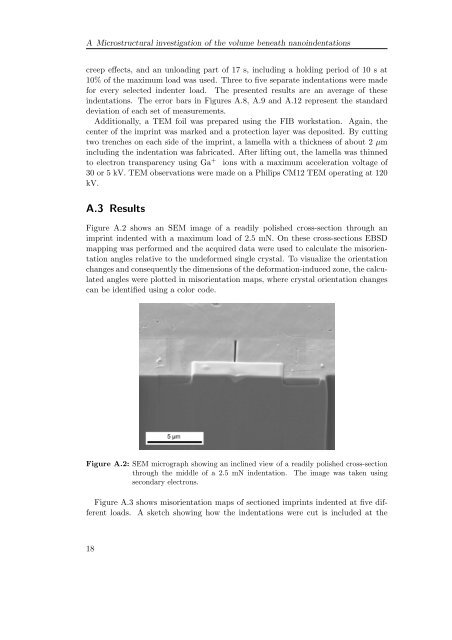
Figure A.2 shows an SEM image <strong>of</strong> a readily polished cross-section through an<br />
impr<strong>in</strong>t <strong>in</strong>dented with a maximum load <strong>of</strong> 2.5 mN. On these cross-sections EBSD<br />
mapp<strong>in</strong>g was performed and the acquired data were used to calculate the misorientation<br />
angles relative to the undeformed s<strong>in</strong>gle crystal. To visualize the orientation<br />
changes and consequently the dimensions <strong>of</strong> the deformation-<strong>in</strong>duced zone, the calculated<br />
angles were plotted <strong>in</strong> misorientation maps, where crystal orientation changes<br />
can be identified us<strong>in</strong>g a color code.<br />
Figure A.2: SEM micrograph show<strong>in</strong>g an <strong>in</strong>cl<strong>in</strong>ed view <strong>of</strong> a readily polished cross-section<br />
through the middle <strong>of</strong> a 2.5 mN <strong>in</strong>dentation. The image was taken us<strong>in</strong>g<br />
secondary electrons.<br />
Figure A.3 shows misorientation maps <strong>of</strong> sectioned impr<strong>in</strong>ts <strong>in</strong>dented at five different<br />
loads. A sketch show<strong>in</strong>g how the <strong>in</strong>dentations were cut is <strong>in</strong>cluded at the<br />
18