

AN-6094 Design Guideline for Flyback Charger Using FAN302HL/UL
AN-6094 Design Guideline for Flyback Charger Using FAN302HL/UL
AN-6094 Design Guideline for Flyback Charger Using FAN302HL/UL

You also want an ePaper? Increase the reach of your titles
YUMPU automatically turns print PDFs into web optimized ePapers that Google loves.
<strong>AN</strong>-<strong>6094</strong><br />
www.fairchildsemi.com<br />
<strong>Design</strong> <strong>Guideline</strong> <strong>for</strong> <strong>Flyback</strong> <strong>Charger</strong> <strong>Using</strong> F<strong>AN</strong>302HL/<strong>UL</strong><br />
1. Introduction<br />
More than half of the external power supplies produced<br />
are used <strong>for</strong> portable electronics such as laptops, cellular<br />
phones, and MP3 players that require constant output<br />
voltage and current regulation <strong>for</strong> battery charging. For<br />
applications requiring precise Constant Current (CC)<br />
regulation, current sensing in the secondary side is always<br />
necessary, which results in sensing loss. For power<br />
supply designers faced with stringent energy-efficiency<br />
regulations, output current sensing is a design challenge.<br />
The advanced PWM controller F<strong>AN</strong>302HL/<strong>UL</strong> can<br />
alleviate the burden of meeting international energy<br />
efficiency regulations in charger designs. The<br />
F<strong>AN</strong>302HL/<strong>UL</strong> family uses a proprietary primary-side<br />
regulation (PSR) technique where the output current is<br />
precisely estimated with only the in<strong>for</strong>mation in the<br />
primary side of the trans<strong>for</strong>mer and controlled with an<br />
internal compensation circuit. This removes the output<br />
AC Line<br />
NA<br />
RVS1<br />
RVS2<br />
Fuse<br />
DA<br />
Bridge<br />
RVDD<br />
CDD<br />
CVS<br />
CDL1<br />
1 CS<br />
2 GATE<br />
3<br />
VDD<br />
LF<br />
CDL2<br />
RGATE<br />
F<strong>AN</strong>302HL/<strong>UL</strong><br />
HV<br />
4 VS<br />
GND 5<br />
8<br />
NC 7<br />
FB 6<br />
+<br />
VDL<br />
-<br />
CFB<br />
RHV<br />
current sensing loss and eliminates all external currentcontrol<br />
circuitry, facilitating a higher efficiency power<br />
supply design without incurring additional costs. A<br />
Green-Mode function with an extremely low operating<br />
current (200 µA) in Burst Mode maximizes the light-load<br />
efficiency, enabling con<strong>for</strong>mance to worldwide Standby<br />
Mode efficiency guidelines.<br />
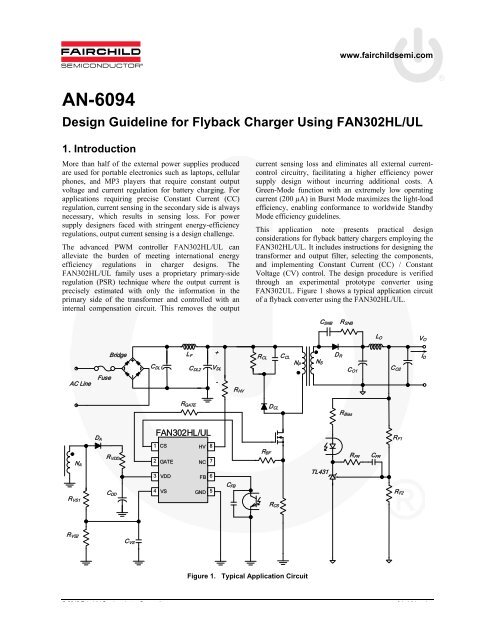
This application note presents practical design<br />
considerations <strong>for</strong> flyback battery chargers employing the<br />
F<strong>AN</strong>302HL/<strong>UL</strong>. It includes instructions <strong>for</strong> designing the<br />
trans<strong>for</strong>mer and output filter, selecting the components,<br />
and implementing Constant Current (CC) / Constant<br />
Voltage (CV) control. The design procedure is verified<br />
through an experimental prototype converter using<br />
F<strong>AN</strong>302<strong>UL</strong>. Figure 1 shows a typical application circuit<br />
of a flyback converter using the F<strong>AN</strong>302HL/<strong>UL</strong>.<br />
© 2012 F i hild S i d t C ti f i hild i<br />
RCL<br />
RBF<br />
DCL<br />
RCS<br />
CCL<br />
NP<br />
Figure 1. Typical Application Circuit<br />
NS<br />
CSNB<br />
TL431<br />
DR<br />
RSNB<br />
CO1<br />
RBias<br />
RFR<br />
LO<br />
CFR<br />
CO2<br />
RF1<br />
RF2<br />
VO<br />
IO
<strong>AN</strong>-<strong>6094</strong><br />
2. Operation Principle<br />
2-1 Constant-Voltage Regulation Operation<br />
Figure 2 shows the internal PWM control circuit of<br />
F<strong>AN</strong>302. The constant voltage (CV) regulation is<br />
implemented in the same way as the conventional isolated<br />
power supply, where the output voltage is sensed using<br />
voltage divider and compared with the internal 2.5 V<br />
reference of the shut regulator (KA431) to generate a<br />
compensation signal. The compensation signal is<br />
transferred to the primary side using an opto-coupler and<br />
applied to the PWM comparator (PWM.V) through<br />
attenuator Av to determine the duty cycle.<br />
CC regulation is implemented internally without directly<br />
sensing the output current. The output current estimator<br />
reconstructs output current in<strong>for</strong>mation (VCCR) using the<br />
trans<strong>for</strong>mer primary-side current and diode current<br />
discharge time. VCCR is then compared with a reference<br />
voltage (2.5 V) by an internal error amplifier and generates<br />
a VEA.I signal to determine the duty cycle.<br />
VEA.I and VEA.V are compared with an internal sawtooth<br />
wave<strong>for</strong>m (VSAW) by PWM comparators PWM.I and<br />
PWM.V, respectively, to determine the duty cycle. As seen<br />
in Figure 2, the outputs of two comparators (PWM.I and<br />
PWM.V) are combined with the OR gate and used as a<br />
reset signal of flip-flop to determine the MOSFET turn-off<br />
instant. The lower signal, VEA.V and VEA.I, determines the<br />
duty cycle, as shown in Figure 3. During CV regulation,<br />
VEA.V determines the duty cycle while VEA.I is saturated to<br />
HIGH. During CC regulation, VEA.I determines the duty<br />
cycle while VEA.V is saturated to HIGH.<br />
Figure 2. Internal PWM Control Circuit<br />
Figure 3. PWM Operation <strong>for</strong> CC and CV<br />
Output Current Estimation<br />
Figure 4 shows the key wave<strong>for</strong>m of a flyback converter<br />
operating in Discontinuous Conduction Mode (DCM),<br />
where the secondary side diode current reaches zero be<strong>for</strong>e<br />
the next switching cycle begins. Since the output current<br />
estimator of F<strong>AN</strong>302 is designed <strong>for</strong> DCM operation, the<br />
power stage should be designed such that DCM is<br />
guaranteed <strong>for</strong> the entire operating range. The output<br />
current is obtained by averaging the triangular output diode<br />
current area over a switching cycle, as calculated by:<br />
AVG NP<br />
tDIS<br />
IO = ID = IPK ⋅ (1)<br />
NS 2tS<br />
where IPK is the peak value of the primary-side current;<br />
NP and NS are the number of turns of the trans<strong>for</strong>mer,<br />
primary side and secondary side, respectively; tDIS is the<br />
diode current discharge time; and ts is switching period.<br />
© 2012 Fairchild Semiconductor Corporation www.fairchildsemi.com<br />
Rev. 1.0.0 • 9/27/12 2<br />
I P K<br />
I<br />
PK<br />
N<br />
⋅<br />
N<br />
N<br />
A VO ⋅<br />
NS<br />
P<br />
S<br />
I = I<br />
AVG<br />
D O<br />
Figure 4. Key Wave<strong>for</strong>ms of DCM <strong>Flyback</strong> Converter
<strong>AN</strong>-<strong>6094</strong><br />
3. <strong>Design</strong> Consideration<br />
A battery charger power supply with CC output requires<br />
more design consideration than the conventional power<br />
supply with a fixed output voltage. In CC operation, the<br />
output voltage changes according to the charging<br />
condition of battery. The supply voltage <strong>for</strong> the PWM<br />
controller (VDD), which is usually obtained from the<br />
auxiliary winding of the trans<strong>for</strong>mer, changes with the<br />
output voltage. Thus, the allowable VDD operation range<br />
determines the output voltage variation range in CC<br />
regulation. F<strong>AN</strong>302 has a wide supply voltage (VDD)<br />
operation range from 5 V up to 26.5 V, which allows<br />
stable CC regulation even with output voltage lower than<br />
a quarter of its nominal value.<br />
Another important design consideration <strong>for</strong> CC operation<br />
is that the trans<strong>for</strong>mer should be designed to guarantee<br />
DCM operation over the whole operation range since the<br />
output current can be properly estimated only in DCM, as<br />
described in Section 2. As seen in Figure 5, the MOSFET<br />
conduction time (tON) decreases as output voltage<br />
decreases in CC Mode, which is proportional to the square<br />
root of the output voltage. Meanwhile, the diode current<br />
discharge time (tDIS) increases as the output voltage<br />
decreases, which is inversely proportional to the output<br />
voltage. Since the increase of tDIS is dominant over the<br />
decrease of tON in determining the sum of tON and tDIS, the<br />
sum of tON and tDIS tends to increases as output voltage<br />
decreases. When the sum of tON and tDIS are same as the<br />
switching period, the converter enters CCM. F<strong>AN</strong>302 has<br />
Figure 5. Operation Range of <strong>Charger</strong> with CC/CV<br />
a frequency-reduction function to prevent CCM operation<br />
by extending the switching period as the output voltage<br />
drops, as illustrated in Figure 6. The output voltage is<br />
indirectly sensed by sampling the trans<strong>for</strong>mer winding<br />
voltage (VSH) around the end of diode current discharge<br />
time, as illustrated in Figure 4. The frequency-reduction<br />
profile is designed such that the on-time remains almost<br />
constant even when the output voltage drops in CC Mode.<br />
Δf<br />
= S<br />
ΔV<br />
© 2012 Fairchild Semiconductor Corporation www.fairchildsemi.com<br />
Rev. 1.0.0 • 9/27/12 3<br />
G−CC<br />
Figure 6. Frequency Reduction in CC Mode
<strong>AN</strong>-<strong>6094</strong><br />
4. <strong>Design</strong> Procedure<br />
In this section, a design procedure is presented using the<br />
Figure 1 as a reference. An offline charger with 6 W / 5 V<br />
output has been selected as a design example. The design<br />
specifications are:<br />
Line Voltage Range: 90~264 VAC and 60 Hz<br />
Nominal Output Voltage and Current: 5 V / 1.2 A<br />
Output Voltage Ripple: Less than 100 mV<br />
Minimum Output Voltage in CC Mode: 25% of<br />
Nominal Output (1.25 V)<br />
Maximum Switching Frequency: 140 kHz<br />
Figure 7. Output Voltage and Current Operating Area<br />
[STEP-1] Estimate the Efficiencies<br />
The charger application has output voltage and current<br />
that change over a wide range, as shown in Figure 7,<br />
depending on the charging status of the battery. Thus, the<br />
efficiencies and input powers of various operating<br />
conditions should be specified to optimize the power stage<br />
design. The critical operating points <strong>for</strong> design:<br />
Operating Point A, where the output voltage and<br />
current reach maximum value (nominal output<br />
voltage and current).<br />
Operating Point B, where the frequency drop is<br />
initiated to maintain DCM operation.<br />
Operating Point C, where the output has its<br />
minimum voltage in CC Mode.<br />
Typically, low line is the worst case <strong>for</strong> the trans<strong>for</strong>mer<br />
design since the largest duty cycle occurs at the minimum<br />
input voltage condition. As a first step, the following<br />
parameters should be estimated <strong>for</strong> low line.<br />
Estimated overall efficiency <strong>for</strong> operating points A, B,<br />
and C (EFF@A, EFF@B, and EFF@C): The overall power<br />
conversion efficiency should be estimated to calculate<br />
the input power and maximum DC link voltage ripple.<br />
If no reference data is available, use the typical<br />
efficiencies in Table 1.<br />
Estimated primary-side efficiency (EFF.P) and<br />
secondary-side efficiency (EFF.S) <strong>for</strong> operating point A,<br />
B, and C. Figure 8 shows the definition of primaryside<br />
and secondary-side efficiencies. The primary-side<br />
efficiency is <strong>for</strong> the power transferred from the AC<br />
line to the trans<strong>for</strong>mer primary side. The secondaryside<br />
efficiency is <strong>for</strong> the power transferred from the<br />
trans<strong>for</strong>mer primary side to the power supply output.<br />
Since the rectifier diode <strong>for</strong>ward voltage drop does not<br />
change much with its voltage rating, the conduction loss<br />
of output rectifier diode tends to be dominant <strong>for</strong> a low<br />
output voltage application. There<strong>for</strong>e, the distribution of<br />
primary-side and secondary-side efficiencies changes with<br />
the output voltage. With a given trans<strong>for</strong>mer efficiency,<br />
the secondary- and primary-side efficiency, ignoring the<br />
diode switching loss, are given as:<br />
N<br />
VO<br />
FF. S ≅ FF. TX ⋅<br />
N<br />
VO + VF<br />
E E<br />
EFF. P = EFF / EFF.<br />
S<br />
(3)<br />
where EFF.TX is trans<strong>for</strong>mer efficiency, typically<br />
0.95~0.98%; VO N is the nominal output voltage; and<br />
VF is the rectifier diode <strong>for</strong>ward-voltage drop.<br />
© 2012 Fairchild Semiconductor Corporation www.fairchildsemi.com<br />
Rev. 1.0.0 • 9/27/12 4<br />
(2)<br />
Table 1. Typical Efficiency of <strong>Flyback</strong> Converter<br />
Output<br />
Voltage<br />
Typical Efficiency at Minimum<br />
Line Voltage<br />
Universal Input European Input<br />
3.3 ~ 6 V 65 ~ 70% 67 ~ 72%<br />
6 ~ 12 V 70 ~ 77% 72 ~ 79%<br />
12 ~ 24 V 77 ~ 82% 79 ~ 84%<br />
Figure 8. Primary-Side and Secondary-Side Efficiency<br />
With the estimated overall efficiency, the input power at<br />
operating point A is given as:<br />
P<br />
IN @ A<br />
N N<br />
VO<br />
IO<br />
= (4)<br />
E<br />
FF @ A<br />
where VO N and IO N are the nominal output voltage and<br />
current, respectively.
<strong>AN</strong>-<strong>6094</strong><br />
The input power of trans<strong>for</strong>mer at operating point A is<br />
given as:<br />
P<br />
IN. T @A<br />
V<br />
=<br />
E<br />
N N<br />
O IO<br />
FF. S @A<br />
To reduce the switching frequency as the output voltage<br />
drops in CC Mode <strong>for</strong> maintaining DCM operation, the<br />
output voltage needs to be sensed. F<strong>AN</strong>302 senses the<br />
output voltage indirectly by sampling auxiliary winding<br />
voltage just be<strong>for</strong>e the diode conduction finishes, as<br />
explained with Figure 4 in Section 2. Since the switching<br />
frequency starts decreasing as VS sampling voltage drops<br />
below 2.15 V, as illustrated in Figure 6, the output voltage<br />
at operating point B can be obtained as:<br />
2.15<br />
V = ⋅ ( V + V ) −V<br />
N<br />
O@ B<br />
VSH<br />
@ A<br />
O F. SH F. SH<br />
where VSH@A is the VS sampling voltage at operating<br />
point A, which is typically designed as 2.5 V and VF.SH<br />
is the rectifier diode <strong>for</strong>ward voltage drop at the VS<br />
sampling instant (85% of diode conduction time), which<br />
is typically about 0.1 V. Note that VF.SH is less than a<br />
third of VF since the Vs voltage sampling occurs when<br />
the diode current is very small.<br />
The overall efficiency at operating point B, where the<br />
frequency reduction starts, can be estimated as:<br />
V V V<br />
N<br />
O@B O + F<br />
FF@B≅ FF @A⋅<br />
⋅<br />
N<br />
VO@B + VF VO<br />
E E<br />
Note that the efficiency changes as the output voltage<br />
drops in CC Mode. The efficiency should be also<br />
estimated <strong>for</strong> each operating point (B and C).<br />
The secondary-side efficiency at operating point B can be<br />
estimated as:<br />
V V V<br />
N<br />
O@B O + F<br />
FF. S@ B ≅ FF. S @A⋅<br />
⋅<br />
N<br />
VO@B + VF VO<br />
E E<br />
Then, the power supply input power and trans<strong>for</strong>mer input<br />
power at operating point B are given as:<br />
P<br />
IN @B<br />
N<br />
O@B⋅O V I<br />
=<br />
E<br />
FF@ B<br />
N<br />
O@B ⋅ O<br />
V I<br />
PIN.<br />
T @B=<br />
(10)<br />
EFF.<br />
S@B The overall efficiency at operating point C can be<br />
approximated as:<br />
V V V<br />
N<br />
O@C O + F<br />
FF@ C ≅ FF ⋅ ⋅<br />
N<br />
VO@C + VF VO<br />
E E<br />
(5)<br />
(6)<br />
(7)<br />
(8)<br />
(9)<br />
(11)<br />
where VO@C is the minimum output voltage <strong>for</strong> CC<br />
Mode at operating point C.<br />
The secondary-side efficiency at operating point C can be<br />
estimated as:<br />
V V V<br />
N<br />
O@C O + F<br />
FF. S@ C ≅ FF. S @A⋅<br />
⋅<br />
N<br />
VO@C + VF VO<br />
E E<br />
(12)<br />
Then, the power supply input power and trans<strong>for</strong>mer input<br />
power at operating point C are given as:<br />
N<br />
O@C ⋅ O<br />
© 2012 Fairchild Semiconductor Corporation www.fairchildsemi.com<br />
Rev. 1.0.0 • 9/27/12 5<br />
P<br />
IN @C<br />
P<br />
IN. T @C<br />
V I<br />
= (13)<br />
E<br />
FF @C<br />
N<br />
O@C ⋅ O<br />
V I<br />
= (14)<br />
E<br />
FF. S @C<br />
(<strong>Design</strong> Example)<br />
To maximize efficiency, a low-voltage-drop Schottky<br />
diode whose <strong>for</strong>ward voltage drop is 0.35 V is selected.<br />
Assuming the overall efficiency is 73% and the<br />
trans<strong>for</strong>mer efficiency is 97% at operating point A<br />
(nominal output voltage and current) <strong>for</strong> low line, the<br />
secondary-side efficiency is obtained as:<br />
N<br />
VO<br />
FF. S @ A ≅ FF. TX ⋅ = 0.907<br />
N<br />
VO + VF<br />
E E<br />
Then, the input powers of the power supply and<br />
trans<strong>for</strong>mer at operating point A are obtained as:<br />
N N<br />
VO<br />
IO<br />
6<br />
PIN<br />
@ A = = = 8.22W<br />
E 0.73<br />
FF @ A<br />
N N<br />
VO IO<br />
6<br />
PIN.<br />
T @A=<br />
= = 6.62W<br />
EFF.<br />
S @A<br />
0.907<br />
The efficiencies at operating point B are:<br />
N<br />
VO@B VO + VF<br />
EFF @B≅ EFF<br />
@A⋅<br />
⋅ = 0.722<br />
N<br />
VO@B + VF VO<br />
N<br />
VO@B VO + VF<br />
EFF . S @ B ≅ EFF.<br />
S @A⋅<br />
⋅ = 0.896<br />
N<br />
VO@B + VF VO<br />
Then, the input powers of the power supply and<br />
trans<strong>for</strong>mer at operating point B are obtained as:<br />
N<br />
VO@BIO<br />
PIN<br />
@ B = = 7.07W<br />
EFF<br />
@ B<br />
N<br />
VO@BIO<br />
PIN<br />
. T @B<br />
= = 5.69W<br />
EFF.<br />
S @B<br />
The primary-side and secondary-side efficiencies at the<br />
operating point C are calculated as:<br />
N<br />
VO@C VO + VF<br />
EFF @C≅ EFF<br />
@A⋅<br />
⋅ = 0.610<br />
N<br />
VO@C + VF VO<br />
N<br />
VO@C VO + VF<br />
EFF. S@ C ≅ EFF.<br />
S @A⋅<br />
⋅ = 0.758<br />
N<br />
VO@C + VF VO<br />
Then, the input powers of the power supply and<br />
trans<strong>for</strong>mer at operating point C are obtained as:<br />
N<br />
VO@C<br />
⋅ IO<br />
PIN<br />
@C<br />
= = 2.46W<br />
EFF<br />
@C<br />
N<br />
VO@C<br />
⋅ IO<br />
PIN<br />
. T @C<br />
= =<br />
1.98W<br />
E<br />
FF. S @C
<strong>AN</strong>-<strong>6094</strong><br />
[STEP-2] Determine the DC Link Capacitor<br />
(CDL) and the DC Link Voltage Range<br />
It is typical to select the DC link capacitor as 2-3 µF per<br />
watt of input power <strong>for</strong> universal input range (90-<br />
264 VAC) and 1 µF per watt of input power <strong>for</strong> European<br />
input range (195~265 Vrms). With the DC link capacitor<br />
chosen, the minimum DC link voltage is obtained as:<br />
P min min 2 IN@A(1 − Dch)<br />
VDL@ A = 2( ⋅ VLINE)<br />
−<br />
(15)<br />
CDL ⋅ fL<br />
where VLINE min is the minimum line voltage; CDL is the<br />
DC link capacitor; fL is the line frequency; and Dch is<br />
the DC link capacitor charging duty ratio defined as<br />
shown in Figure 9, which is typically about 0.2.<br />
The maximum DC link voltage is given as:<br />
max max<br />
VDL = 2 ⋅VLINE<br />
(16)<br />
where VLINE max is the maximum line voltage.<br />
The minimum DC link voltage and its ripple change with<br />
input power. The minimum input DC link voltage at<br />
operating point B is given as:<br />
P min min 2 IN@B(1 − Dch)<br />
VDL@ B = 2( ⋅ VLINE)<br />
−<br />
C ⋅ f<br />
DL L<br />
(17)<br />
The minimum input DC link voltage at operating point C<br />
is given as:<br />
P min min 2 IN@C(1 − Dch)<br />
VDL@C = 2( ⋅ VLINE<br />
) −<br />
C ⋅ f<br />
DL L<br />
(18)<br />
Figure 9. DC Link Voltage Wave<strong>for</strong>ms<br />
(<strong>Design</strong> Example) By choosing two 6.8 µF capacitors<br />
in parallel <strong>for</strong> the DC link capacitor, the minimum and<br />
maximum DC link voltages <strong>for</strong> each condition are<br />
obtained as:<br />
P min min 2 IN @ A(1 − Dch)<br />
VDL@ A = 2( ⋅ VLINE)<br />
−<br />
CDL ⋅ fL<br />
2 8.22(1− 0.2)<br />
= 2 ⋅(90) − = 90V<br />
−6<br />
2⋅ 6.8× 10 ⋅60<br />
V = 2 ⋅ 264 = 373V<br />
max<br />
DL<br />
P min min 2 IN@B(1 − Dch)<br />
VDL@ B = 2( ⋅ VLINE)<br />
−<br />
CDL ⋅ fL<br />
2 7.07(1 − 0.2)<br />
= 2(90) ⋅ − = 96V<br />
−6<br />
26.8 ⋅ × 10⋅60 P min min 2 IN@C(1 − Dch)<br />
VDL@ C = 2( ⋅ VLINE)<br />
−<br />
CDL ⋅ fL<br />
2 2.46(1− 0.2)<br />
= 2 ⋅(90) − = 117V<br />
−6<br />
26.8 ⋅ × 10⋅60 [STEP-3] Determine Trans<strong>for</strong>mer Turns<br />
Ratio<br />
Figure 10 shows the MOSFET drain-to-source voltage<br />
wave<strong>for</strong>ms. When the MOSFET is turned off, the sum of<br />
the input DC link voltage (VDL) and the output voltage<br />
reflected to the primary side is imposed across the<br />
MOSFET, calculated as:<br />
V = V + V<br />
nom max<br />
DS DL RO<br />
© 2012 Fairchild Semiconductor Corporation www.fairchildsemi.com<br />
Rev. 1.0.0 • 9/27/12 6<br />
(19)<br />
where VRO is reflected output voltage, defined as:<br />
N p N<br />
VRO = ( VO + VF)<br />
(20)<br />
N s<br />
where NP and NS are number of turns <strong>for</strong> the primary<br />
side and secondary side, respectively.<br />
When the MOSFET is turned on; the output voltage,<br />
together with input voltage reflected to the secondary, are<br />
imposed across the secondary-side rectifier diode<br />
calculated as:<br />
N<br />
V = V + V<br />
(21)<br />
nom S max N<br />
D<br />
NP<br />
DL O<br />
As observed in Equations (19), (20), and (21); increasing<br />
the trans<strong>for</strong>mer turns ratio (NP / NS) increases voltage<br />
stress on the MOSFET while reducing voltage stress on<br />
the rectifier diode. There<strong>for</strong>e, the NP / NS should be<br />
determined by the trade-off between the MOSFET and<br />
diode voltage stresses.<br />
The trans<strong>for</strong>mer turns ratio between the auxiliary winding<br />
and the secondary winding (NA / NS) should be<br />
determined by considering the allowable IC supply<br />
voltage (VDD) range. The VDD voltage varies with load<br />
condition, as shown in Figure 11, where the minimum<br />
VDD typically occurs at minimum load condition. Due to<br />
the voltage overshoot of the auxiliary winding voltage<br />
caused by the trans<strong>for</strong>mer leakage inductance; the VDD at<br />
operating point C tends to be higher than the VDD at<br />
minimum load condition.<br />
The VDD at minimum load condition is obtained as:<br />
N<br />
V ≅ ( V + V ) −V<br />
(22)<br />
min A<br />
DD<br />
NS<br />
O F FA<br />
where VFA is the diode <strong>for</strong>ward-voltage drop of the<br />
auxiliary winding diode.<br />
The trans<strong>for</strong>mer turns ratio should be determined such<br />
that VDD min is higher than the VDD UVLO voltage, such as:<br />
N A ( V + V ) − V > V + V<br />
N<br />
S<br />
max<br />
O F FA UVLO MRGN<br />
(23)<br />
Since the VDD min is related to standby power consumption,<br />
smaller NA / NS leads to lower standby power<br />
consumption. However, 2~3 V margin (VMRGN) should be
<strong>AN</strong>-<strong>6094</strong><br />
added in to Equation (23), considering the VDD ripple<br />
caused by Burst Mode operation at no-load condition.<br />
NP ( VO + VF)<br />
N<br />
S<br />
VDL<br />
NS VDL + VO<br />
NP<br />
Figure 10. Voltage Stress on MOSFET and Diode<br />
Figure 11. VDD and Winding Voltage<br />
(<strong>Design</strong> Example)<br />
For a 700 V MOSFET to have 35% margin on VDS nom ,<br />
the reflected output voltage should be:<br />
nom<br />
VDS = 373+ VRO< 0.65× 700 = 455V<br />
∴ V < 82V<br />
© 2012 Fairchild Semiconductor Corporation www.fairchildsemi.com<br />
Rev. 1.0.0 • 9/27/12 7<br />
RO<br />
Setting VRO=71 V, NP / NS is obtained as:<br />
NP<br />
VRO<br />
71<br />
= = = 13.27<br />
N ( V + V ) 5.35<br />
S o F<br />
Then, the voltage stress of diode is obtained as:<br />
N<br />
V = V + V = 33.13V<br />
nom S max<br />
D<br />
NP<br />
DL O<br />
The allowable minimum VDD is 5.3 V, considering the<br />
tolerances of UVLO. Considering voltage ripple on VDD<br />
caused by burst operation at no-load condition, a 2 V<br />
margin is added <strong>for</strong> VDD voltage calculation at no-load<br />
condition, calculated as:<br />
N<br />
V V V V V V<br />
min A<br />
DD = (<br />
NS<br />
O + F ) − FA ><br />
max<br />
UVLO + MRGN<br />
N A<br />
(5<br />
NS<br />
0.35) 0.7 5.3 2<br />
+ − > +<br />
N A ∴ > 1.5<br />
N<br />
S<br />
To minimize the power consumption of the IC by<br />
minimizing VDD at no-load condition, NA / NS is<br />
determined as 1.6.<br />
[STEP-4] <strong>Design</strong> the Trans<strong>for</strong>mer<br />
Figure 12 shows the MOSFET conduction time (tON),<br />
diode current discharge time (tDIS), and diode nonconduction<br />
time (tOFF). For the trans<strong>for</strong>mer design, first<br />
determine how much non-conduction time (tOFF) is used in<br />
DCM operation. The diode current discharge time<br />
increases as the output voltage drops in CC Mode. Even<br />
though tON decreases as output voltage drops, tON is<br />
proportional to the square root of the output voltage, while<br />
tDIS is inversely proportional to the output voltage. Thus,<br />
the sum of tON and tDIS tends to increase, which reduces<br />
the tOFF, <strong>for</strong>cing the flyback converter with a fixed<br />
switching frequency into CCM operation as the output<br />
voltage drops.<br />
Thus, operating point B, where the frequency reduction<br />
starts, is the worst case <strong>for</strong> determining the nonconduction<br />
time (tOFF), as illustrated in Figure 12. tOFF<br />
should be large enough to cover the trans<strong>for</strong>mer variation<br />
and frequency hopping. However, too large tOFF increases<br />
RMS current of the primary side current. It is typical to<br />
set tOFF as 15-20% of the switching period.
<strong>AN</strong>-<strong>6094</strong><br />
Once the tOFF is determined at operating point B, the<br />
MOSFET conduction time is obtained as:<br />
1/ fS − tOFF@B<br />
tON<br />
@ B =<br />
min<br />
N V S DL@ B<br />
(1 + ⋅ )<br />
(24)<br />
N P VO@B + VF<br />
Then, the trans<strong>for</strong>mer primary-side inductance can be<br />
calculated as:<br />
min 2<br />
( VDL@B⋅tON@B) Lm = ⋅ fS<br />
(25)<br />
2PIN.<br />
T @B<br />
Once the trans<strong>for</strong>mer primary-side inductance is<br />
determined, DCM operation at operating point C should<br />
be checked. To prevent CCM operation, F<strong>AN</strong>302<br />
decreases the switching frequency as the output voltage<br />
drops, as illustrated in Figure 13. The switching frequency<br />
at the minimum output voltage is obtained as:<br />
Δf<br />
V + V<br />
f f (2.15 V<br />
)<br />
S<br />
O@ C F. SH<br />
S@C = S − − SH@A⋅ N<br />
Δ VSH VO+ VF.<br />
SH<br />
(26)<br />
where ΔfS / ΔVSH is 64 kHz / V <strong>for</strong> <strong>UL</strong> version and<br />
38 kHz / V <strong>for</strong> HL version, and VF.SH is the rectifier<br />
diode <strong>for</strong>ward voltage drop at the VS sampling instant<br />
(85% of diode conduction time).<br />
Then, the MOSFET conduction time at operating point C<br />
is given as:<br />
2P<br />
L<br />
= (27)<br />
1 IN. T@Cm ON @C min<br />
VDL@CfS@C t<br />
The non-conduction time at operating point C is given as:<br />
V<br />
(1 )<br />
min<br />
1<br />
NS<br />
DL@ C<br />
OFF @C= − ON @C+<br />
⋅<br />
fS@C NP VO@C + VF<br />
t t<br />
(28)<br />
The non-conduction time should be larger than 15% of<br />
switching period, considering the trans<strong>for</strong>mer variation<br />
and frequency hopping.<br />
Figure 12. Variation of tON, tD, and tOFF<br />
Figure 13. Frequency Reduction in CC Mode<br />
Once the trans<strong>for</strong>mer primary-side inductance is obtained,<br />
the maximum peak drain current can be calculated at the<br />
nominal output condition (operating point A) as:<br />
2PINT . @A<br />
PK<br />
IDS<br />
=<br />
(29)<br />
Lm⋅fS The minimum number of turns <strong>for</strong> the trans<strong>for</strong>mer<br />
primary side to avoid the core saturation is given by:<br />
© 2012 Fairchild Semiconductor Corporation www.fairchildsemi.com<br />
Rev. 1.0.0 • 9/27/12 8<br />
N<br />
min<br />
P<br />
PK<br />
LmIDS = (30)<br />
B A<br />
sat e<br />
where AE is the cross-sectional area of the core in m 2<br />
and Bsat is the saturation flux density in Tesla. Figure 14<br />
shows the typical characteristics of a ferrite core from<br />
TDK (PC40). Since the saturation flux density (Bsat)<br />
decreases as the temperature rises, the high temperature<br />
characteristics should be considered, especially <strong>for</strong><br />
charger application in an enclosed case. If there is no<br />
reference data, use Bsat=0.25~0.3T. With the turns ratio<br />
obtained in STEP-3, determine the proper integer <strong>for</strong> Ns<br />
min<br />
such that the resulting NP is larger than NP obtained<br />
from Equation (30).<br />
Figure 14. Typical B-H Curves of Ferrite Core<br />
(TDK/PC40)
<strong>AN</strong>-<strong>6094</strong><br />
(<strong>Design</strong> Example) By setting the non conduction time at<br />
operating point B as 1.6 µs, the MOSFET conduction<br />
time is obtained as:<br />
1/ fS −tOFF@B<br />
tON @B = = 2.15μs<br />
min<br />
N V S DL@ B<br />
(1 + ⋅ )<br />
N V + V<br />
P O@B F<br />
The trans<strong>for</strong>mer primary-side inductance is calculated<br />
as:<br />
min 2<br />
( VDL@B⋅tON @B)<br />
Lm = ⋅ fS = 527μ<br />
H<br />
2P<br />
IN . T @B<br />
Assuming VSH@A is 2.5 V, the switching frequency at the<br />
minimum output voltage is obtained as:<br />
Δf<br />
V + V<br />
(2.15 2.5 )<br />
S<br />
O@ C F. SH<br />
S@C = S − − ⋅ N<br />
Δ VSH VO+ VF.<br />
SH<br />
f f<br />
= 45kHz<br />
The MOSFET conduction time at minimum output<br />
voltage is obtained as:<br />
1 2P<br />
L<br />
t = = 1.84μs<br />
IN. T @C<br />
m<br />
ON @C min<br />
VDL@CfS@C The non-conduction time at minimum output voltage:<br />
V<br />
(1 )<br />
min<br />
1<br />
N S DL@ C<br />
OFF @C= − ON @C+<br />
⋅<br />
fS@C NP VO@C + VF<br />
t t<br />
= 10.33μs<br />
The peak drain current at maximum load condition is<br />
given as:<br />
2P<br />
PK IN. T @A<br />
IDS = = 423mA<br />
L ⋅ f<br />
m S<br />
EE12.5 core is selected <strong>for</strong> the trans<strong>for</strong>mer. The<br />
minimum number of turns <strong>for</strong> the trans<strong>for</strong>mer primary<br />
side to avoid the core saturation is given by:<br />
N<br />
min<br />
P<br />
LI<br />
=<br />
B A<br />
PK<br />
m DS<br />
sat e<br />
−6<br />
527× 10 ⋅0.423<br />
= = 63.5<br />
−6<br />
0.3⋅ 12.88× 10<br />
Determine the proper integer <strong>for</strong> Ns such that the<br />
resulting Np is larger than Np min ; given as:<br />
NP = 13.27×<br />
NS<br />
min<br />
= 13.27× 5 = 66 > N<br />
The auxiliary winding turns, NA, is obtained as:<br />
N A NA = × NS<br />
= 1.6× 5 = 8<br />
N<br />
S<br />
P<br />
[STEP-5] Set the Output Current and VS<br />
Sensing Resistor<br />
The nominal output current is determined by the sensing<br />
resistor value and trans<strong>for</strong>mer turns ratio as:<br />
NP× VCCR<br />
RCS<br />
=<br />
N<br />
(31)<br />
2NSIO<br />
× K<br />
where VCCR is 2.43 V and K=12 and 10.5 V <strong>for</strong> <strong>UL</strong> and<br />
HL, respectively.<br />
The voltage divider RVS1 and RVS2 should be determined<br />
so that VS is about 2.5 V at 85% of diode current<br />
conduction time as:<br />
N<br />
RVS1 N A ( VO+ VF.<br />
SH )<br />
= −1(32)<br />
RVS 2 NSVSH@A The F<strong>AN</strong>302 indirectly senses input voltage using the VS<br />
pin current while the MOSFET is turned on, as illustrated<br />
in Figure 15. Since the VS pin voltage is clamped at 0.7 V<br />
when the MOSFET is turned on, the current flowing out<br />
of the VS pin is approximately proportional to the input<br />
voltage, calculated as:<br />
N 1 0.7 N V<br />
I = ( V + 0.7) + ≅ (33)<br />
A A DL<br />
VS. ON<br />
NP DL<br />
RVS1 RVS 2 NPRVS1 Figure 15. VS Pin Current Sensing<br />
F<strong>AN</strong>302 modulates the minimum on-time of the<br />
MOSFET such that it reduces as input voltage increases,<br />
as shown Figure 16. This allows smaller minimum on<br />
time <strong>for</strong> high-line condition, ensuring Burst Mode<br />
operation occurs at almost the same power level<br />
regardless of line voltage variation. The VS current needs<br />
to be higher than 150 µA.<br />
Increasing the minimum on-time by increasing RVS1 and<br />
RVS2 allows F<strong>AN</strong>302 to enter Burst Mode at a higher<br />
power level. This reduces the standby power consumption<br />
by increasing power delivered to the output per switching.<br />
However, this also increases the output voltage ripple by<br />
increasing the time interval between switching bundles in<br />
Burst Mode. Thus, the minimum on-time should be<br />
determined by a trade-off between standby power<br />
consumption and output voltage ripple. When selecting<br />
RVS1 and RVS2, 150 µA is the VS current level to consider<br />
seriously. If the VS current is lower than 150 µA, ton_min<br />
won’t be larger.<br />
© 2012 Fairchild Semiconductor Corporation www.fairchildsemi.com<br />
Rev. 1.0.0 • 9/27/12 9
<strong>AN</strong>-<strong>6094</strong><br />
The recommendation <strong>for</strong> RVS1 design is to set RVS1 such<br />
that the minimum on time curve of Figure 16 can be fully<br />
utilized <strong>for</strong> the universal line range. It is typical to select<br />
RVS1 such that IVS.ON is around 180 µA <strong>for</strong> the minimum<br />
line voltage.<br />
Figure 16. Minimum On-Time vs. VS Pin Current (<strong>UL</strong>)<br />
A bypass capacitor of 22~68 pF placed closely between<br />
the VS and GND pins is recommended to bypass the<br />
switching noise. Too large a capacitor distorts VS voltage<br />
and deteriorates the output current regulation. The RC<br />
time constant of the bypass capacitor and voltage divider<br />
resistor should be
<strong>AN</strong>-<strong>6094</strong><br />
Once the power dissipation in the snubber is obtained, the<br />
snubber resistor is calculated as:<br />
2<br />
( VRO + VOS)<br />
RCL<br />
=<br />
(38)<br />
PCLMP<br />
where RCL is the clamping resistor.<br />
The maximum ripple of the clamping capacitor voltage is<br />
obtained as:<br />
VRO + VOS<br />
Δ VCL<br />
=<br />
(39)<br />
CCLRCL fs<br />
In general, 5~10% ripple of the selected capacitor voltage<br />
is reasonable. The clamping capacitor should be ceramic<br />
or a material that offers low ESR. Electrolytic or tantalum<br />
capacitors are unacceptable.<br />
NP ( VO + VF)<br />
N<br />
S<br />
VDL<br />
Figure 17. RCD Clamping Circuit and Wave<strong>for</strong>ms<br />
The leakage inductance measured with an LCR meter<br />
tends to be larger than the actual effective leakage<br />
inductance. Moreover, the effective output capacitance of<br />
the MOSFET is difficult to measure. The best way to<br />
obtain these parameters correctly is to use the drain<br />
voltage wave<strong>for</strong>m as illustrated in Figure 18. Since Lm can<br />
be measured with an LCR meter, COSS and LLK can be<br />
calculated from the measured resonant period.<br />
In the clamping design in this section, the lossy discharge<br />
of the inductor and stray capacitance is not considered. In<br />
the actual converter, the loss in the clamping network is<br />
less than the designed value due to this effect.<br />
2π LLKCOSS 2π LC m OSS<br />
Figure 18. Drain Voltage Wave<strong>for</strong>m<br />
(<strong>Design</strong> Example) Assuming that 700 V MOSFET is<br />
used, the voltage overshoot to limit the maximum drain<br />
voltage below 600 V is:<br />
max<br />
VOS < 600V −VDL − VRO<br />
= 156<br />
The leakage inductance and the effective output<br />
capacitance of MOSFET are calculated from the<br />
resonance wave<strong>for</strong>m as 18 µH and 55 pF, respectively.<br />
The peak current of clamping diode is obtained as:<br />
PK PK 2 COSS<br />
2<br />
ICL = ( IDS ) − VOS = 325mA<br />
L<br />
© 2012 Fairchild Semiconductor Corporation www.fairchildsemi.com<br />
Rev. 1.0.0 • 9/27/12 11<br />
LK<br />
The power dissipation in the clamping circuit is<br />
obtained as:<br />
1<br />
PK 2 VRO + VOS<br />
PCLMP = fSLLK( ICL ) = 0.194W<br />
2<br />
VOS<br />
Then the clamping circuit resistor is calculated as:<br />
2<br />
( VRO + VOS<br />
)<br />
RCL = = 263kΩ<br />
PCLMP<br />
The actual drain voltage can be lower than the design<br />
due to the loss of stray resistance of inductor and<br />
capacitor. The resistor value can be adjusted after the<br />
power supply is actually built.<br />
To allow less than 15 V ripple on the clamping<br />
capacitor voltage, the clamping capacitor should be:<br />
VRO + VOS<br />
CCL > = 410 pF<br />
C ΔV<br />
f<br />
CL CL s<br />
A 470 pF capacitor is selected.<br />
[STEP-7] Calculate the Voltage and Current<br />
of the Switching Devices<br />
Primary-Side MOSFET: The voltage stress of the<br />
MOSFET was discussed when determining the<br />
trans<strong>for</strong>mer turns ratio in STEP-6. The maximum voltage<br />
stress of the MOSFET is given in Equations (35).<br />
The rms current through the MOSFET is given as:<br />
t f<br />
3<br />
rms PK ON @ A s<br />
DS = (40)<br />
DS<br />
I I
<strong>AN</strong>-<strong>6094</strong><br />
t<br />
where tON is MOSFET conduction time minimum input<br />
voltage and maximum load condition, given as:<br />
ON<br />
2P<br />
L<br />
= (41)<br />
V f<br />
1<br />
min<br />
IN. T@Am DL S<br />
Secondary-Side Diode: The nominal reverse voltage of<br />
the diode is given in Equation (21).<br />
The rms current of the rectifier diode is obtained as:<br />
rms PK N t P DIS @ A ⋅ fS<br />
ID = IDS<br />
⋅ (42)<br />
N 3<br />
S<br />
(<strong>Design</strong> Example) The maximum voltage across the<br />
MOSFET is calculated as:<br />
max<br />
Vds max<br />
= VDL + VRO+ VOS = 373 + 71+ 155 = 599V<br />
The rms current though the MOSFET is:<br />
rms PK<br />
IDS = IDS tON fs<br />
3<br />
= 0.14A<br />
The diode voltage and current are obtained as:<br />
NS<br />
max 5<br />
VD = VO + VDL = 5 + ⋅ 373 = 33.1V<br />
NP<br />
66<br />
rms PK N tDIS @ A ⋅ f<br />
P<br />
S<br />
ID = IDS ⋅ = 2.14A<br />
N 3<br />
S<br />
[STEP-8] Determine the Output Filter Stage<br />
The peak-to-peak ripple of capacitor current is given as:<br />
N<br />
Δ I = I<br />
P PK<br />
C<br />
NS<br />
DS<br />
The voltage ripple on the output is given by:<br />
(43)<br />
N 2<br />
tDIS @ A ( ΔIC − IO<br />
)<br />
Δ VO = ⋅ +ΔIC ⋅RC<br />
(44)<br />
2CO<br />
ΔIC<br />
Sometimes it is impossible to meet the ripple specification<br />
with a single-output capacitor due to the high ESR of the<br />
electrolytic or tantalum capacitors. Additional LC filter<br />
stages (post filter) can be used. When using post filters, do<br />
not place the corner frequency too low. Too low corner<br />
frequency may make the system unstable or limit the<br />
control bandwidth. It is typical to set the corner frequency<br />
of the post filter at around 1/10~1/5 of the switching<br />
frequency.<br />
(<strong>Design</strong> Example) Assuming a 330 µF tantalum<br />
capacitor with 100 mΩ ESR <strong>for</strong> the output capacitor, the<br />
voltage ripple on the output is:<br />
NP<br />
PK<br />
Δ IC = IDS = 5.59A<br />
NS<br />
N 2<br />
tDIS @ A ( ΔIC − IO<br />
)<br />
Δ VO = ⋅ +ΔIC ⋅ RC = 0.592V<br />
2CO<br />
ΔIC<br />
Since the output voltage ripple exceeds the specification<br />
of 100 mV, a post LC filter should be used. Two 330 µF<br />
capacitors and one 1.8 µH inductor are selected <strong>for</strong> the<br />
post LC filter. Then, the cutoff frequency of the LC filter<br />
is 9.2 kHz.<br />
[STEP-9] Complete the RC Snubber <strong>Design</strong><br />
<strong>for</strong> the Diode<br />
When the primary-side MOSFET is turned on, severe<br />
voltage oscillation occurs across the secondary-side diode,<br />
as shown in Figure 19. This is caused by the oscillation<br />
between the diode parasitic capacitance (CD) and<br />
trans<strong>for</strong>mer secondary-side leakage inductance (LLKS). To<br />
reduce the oscillation, an RC snubber is typically used, as<br />
shown in Figure 19. To effectively introduce damping to<br />
the resonant circuit, the parameters of the RC snubber<br />
should be:<br />
LLKS<br />
RSNB<br />
= (45)<br />
C<br />
© 2012 Fairchild Semiconductor Corporation www.fairchildsemi.com<br />
Rev. 1.0.0 • 9/27/12 12<br />
D<br />
CSNB = 2~3times<br />
of CD<br />
(46)<br />
The secondary-side leakage inductance and the diode<br />
parasitic capacitance are difficult to measure with an LCR<br />
meter. The best way is to use a test capacitor across the<br />
diode. First, measure the natural resonance period (tR)<br />
without connecting anything to the diode. Then, add a test<br />
capacitor across the diode (CTST) such that the test<br />
resonance period (tRT) becomes about twice its original<br />
value and measure the test resonance period. With the<br />
measured tR, tRT, and CTST; the resonance parameters can<br />
be calculated as:<br />
t<br />
C = C − (47)<br />
L<br />
D<br />
RT 2<br />
TST /[( )<br />
tR<br />
1]<br />
LKS<br />
tR<br />
2 1<br />
( )<br />
2π<br />
CD<br />
= (48)<br />
2π LLKSCD Figure 19. Diode Voltage Wave<strong>for</strong>m
<strong>AN</strong>-<strong>6094</strong><br />
(<strong>Design</strong> Example) The original resonance period is<br />
measured as tR=25 ns.<br />
<strong>Using</strong> a 1 nF test capacitor, the resonance period is<br />
measure as tRT=25 ns.<br />
Then, the resonant parameters are obtained as:<br />
t<br />
C C pF<br />
D = RT 2<br />
TST /[( ) − 1] = 395<br />
tR<br />
tR<br />
2 1<br />
LKS = ( )<br />
2π<br />
CD<br />
= 40<br />
L nH<br />
The snubber circuit parameters are calculated as:<br />
RSNB =<br />
LLKS<br />
C<br />
= 10 Ω , CSNB= 2.5CD= 1nF<br />
D<br />
[STEP-10] <strong>Design</strong> the Feedback Loop<br />
Since the F<strong>AN</strong>302 operates a flyback converter in DCM<br />
with a peak-current mode control, the control to output<br />
transfer function of the power stage is given as:<br />
vˆ o 1+<br />
s ωZ<br />
= GV<br />
⋅ (49)<br />
vˆ1+ s ω<br />
FB P<br />
where<br />
2<br />
ω = ;<br />
p<br />
RC L OUT<br />
1<br />
ω Z = ; COUT is<br />
RESCOUT effective output capacitance; and RES is the effective<br />
series resistance of the output capacitor.<br />
The gain GV of Equation (49) is defined as:<br />
N<br />
1 m VO<br />
GV<br />
= ⋅ ⋅<br />
(50)<br />
3 m+ ma RCSIDS where 1/3 is the attenuation factor of feedback voltage;<br />
IDS is the peak drain current at given operating<br />
condition; ma is the slope of slope compensation signal;<br />
and m is the slope of current sensing signal, given as:<br />
VDL⋅RCS m =<br />
(51)<br />
Lm<br />
Note that the effect of slope compensation is weaker at<br />
high line, which increases the gain of control-to-output<br />
transfer function. Thus, the high line is the worst case <strong>for</strong><br />
feedback loop design.<br />
Since the control to output transfer function is first order,<br />
the feedback control loop can be implemented with a onepole<br />
and one-zero compensation circuit, as shown in<br />
Figure 20. The transfer function of the compensation<br />
network is given as:<br />
vˆ<br />
EA ωI<br />
( s ωCZ1<br />
+ 1)<br />
= ⋅<br />
(52)<br />
vˆ o s ( s ωCP1+<br />
1)<br />
RFB<br />
1<br />
where ω I = ; ω CZ1<br />
=<br />
;<br />
R R C<br />
( R + R ) C<br />
and CP1<br />
F1bias FR<br />
1<br />
ω = .<br />
RFBCFB FR F1 FR<br />
Note that the opto-coupler introduces a mid-frequency<br />
pole due to the collector-emitter junction capacitance.<br />
Since the collector-base junction in a photo-transistor is<br />
used as a light detector; its area is relatively large, which<br />
introduces a large effective collector-emitter junction<br />
capacitance. The typical collector-emitter junction<br />
capacitance is about 3-10 nF <strong>for</strong> the opto-coupler<br />
FOD817A, which brings a pole at around 1 kHz with a<br />
bias resistor of 42 kΩ, as shown in Figure 20. This pole<br />
can occur around the desired crossover frequency, making<br />
the system unstable. There<strong>for</strong>e, this additional pole should<br />
be considered when designing the compensation network.<br />
Figure 20. Feedback Loop Circuit<br />
Figure 21. Frequency Response of Opto-Coupler<br />
© 2012 Fairchild Semiconductor Corporation www.fairchildsemi.com<br />
Rev. 1.0.0 • 9/27/12 13
<strong>AN</strong>-<strong>6094</strong><br />
(<strong>Design</strong> Example) In STEP-8, the post LC filter is<br />
designed with two 330 µF capacitors and a 1.8 µH<br />
inductor. Since the resonance frequency of the post LC<br />
filter is 9.2 kHz, the bandwidth of the feedback loop<br />
should be less than 1/3 of the cut-off frequency to<br />
minimize the phase drop caused by the post LC filter.<br />
Thus, the target bandwidth of the feedback loop is<br />
determined as around 3 kHz.<br />
To simplify analysis, the inductor of the post filter is<br />
ignored, since the bandwidth is below the cutoff<br />
frequency of post LC filter. The effective output<br />
capacitance and its effective series resistance are given as:<br />
C = 330μF× 2 = 660μF<br />
OUT<br />
R = 100 mΩ / 2 = 50mΩ<br />
ES<br />
The slope of current sensing signal <strong>for</strong> high line is<br />
obtained as:<br />
VDL ⋅ RCS373V ⋅1.2<br />
m= = = 0.845 V / μs<br />
L 530μH<br />
m<br />
The slope of internal slope compensation is obtained as:<br />
0.3V 0.3V<br />
ma= = = 0.066 V / μs<br />
1/ fS× Dmax 7.14μs× 0.64<br />
Then, the gain GV <strong>for</strong> high line and maximum load<br />
condition is obtained as:<br />
1 m VO<br />
GV<br />
= ⋅ ⋅<br />
PK<br />
3 m+ ma RCS IDS<br />
= 3<br />
The system pole and zero are obtained as:<br />
2<br />
ω p =<br />
RC<br />
= 727 rad / s<br />
L OUT<br />
N<br />
1<br />
ω Z = = 30,300 rad / s<br />
RESCOUT With RF=0 Ω, CFR=10 nF, Rbias=1 kΩ, RF1=50 kΩ,<br />
CFB=4nF (including output capacitance of optotransistor),<br />
and RFB=42 kΩ; 3 kHz bandwidth with 53 °<br />
phase margin is obtained. For CFB, output capacitance of<br />
an opto-transistor is assumed to be 3 nF and a 1 nF<br />
external capacitor is used.<br />
[STEP-11] Choose Startup Resistor <strong>for</strong> HV Pin<br />
Figure 22 shows the high-voltage (HV) startup circuit <strong>for</strong><br />
F<strong>AN</strong>302 applications. Internally, the JFET is used to<br />
implement the high-voltage current source, whose<br />
characteristics are shown in Figure 23. Technically, the<br />
HV pin can be directly connected to the DC link (VDL).<br />
However, to improve reliability and surge immunity, it is<br />
typical to use a ~100 kΩ resistor between the HV pin and<br />
the DC link. The actual HV current with a given DC link<br />
voltage and startup resistor is determined by the<br />
intersection point of V-I characteristics line and load line,<br />
as shown in Figure 23.<br />
During startup, the internal startup circuit is enabled and<br />
the DC link supplies the current, IHV, to charge the holdup<br />
capacitor, CDD, through RHV. When the VDD voltage<br />
reaches VDD-ON, the internal HV startup circuit is disabled<br />
and the IC starts PWM switching. Once the HV startup<br />
circuit is disabled, the energy stored in CDD should supply<br />
the IC operating current until the trans<strong>for</strong>mer auxiliary<br />
winding voltage reaches the nominal value. There<strong>for</strong>e,<br />
CDD should be properly designed to prevent VDD from<br />
dropping to VDD-OFF be<strong>for</strong>e the auxiliary winding builds up<br />
enough voltage to supply VDD.<br />
The startup time with a given CDD capacitor is given as:<br />
CDDVDD. ON<br />
tstart<br />
=<br />
(53)<br />
( IHV − IDD−ST) Figure 22. HV Startup Circuit<br />
100V 200V 300V 400V<br />
© 2012 Fairchild Semiconductor Corporation www.fairchildsemi.com<br />
Rev. 1.0.0 • 9/27/12 14<br />
V<br />
R<br />
DL<br />
HV<br />
3.5mA<br />
1.5mA<br />
0.8mA<br />
IHV<br />
I<br />
HV<br />
V −V<br />
=<br />
R<br />
DL HV<br />
HV<br />
500V<br />
VHV<br />
VDL<br />
Figure 23. V-I Characteristics of HV Pin<br />
(<strong>Design</strong> Example) With 100 kΩ HV resistor and 33 µF<br />
VDD capacitor, the maximum startup time is:<br />
CDDVDD. ON 33μ ⋅16V<br />
tstart<br />
= = = 1.32s<br />
( I −I) 0.8mA −0.4mA<br />
HV DD−ST
<strong>AN</strong>-<strong>6094</strong><br />
[STEP-12] Protection Setting<br />
Output OVP:<br />
In STEP-5, the voltage divider <strong>for</strong> VS is determined such<br />
that VS sampling voltage is about 2.5 V in normal<br />
operation. The voltage divider also determines the output<br />
over-voltage protection (OVP) level. The OVP is<br />
triggered when VS sampling voltage is above 2.8 V. The<br />
OVP trip point is given as:<br />
OVP NS RVS1+ RVS2<br />
VO = 2.8<br />
−VF.<br />
SH<br />
(54)<br />
NA RVS2<br />
Pulse-by-Pulse Current Limit:<br />
Since F<strong>AN</strong>302 employs current-mode control, the<br />
MOSFET drain current is regulated properly by the error<br />
amplifier output in normal operation. During the load<br />
transient or abnormal condition such as output short, the<br />
error amplifier can be saturated HIGH and the drain<br />
current is regulated by the pulse-by-pulse current limit,<br />
which <strong>for</strong>ces the MOSFET gate to be turned off when the<br />
current-sensing voltage reaches 0.7 V. The flux density of<br />
the trans<strong>for</strong>mer during the pulse-by-pulse current-limit<br />
mode should be checked to make sure that the flux density<br />
is below 0.4~0.42T to prevent severe core saturation.<br />
LV / R<br />
= (55)<br />
N A<br />
OCP m STH CS<br />
MAX<br />
P e<br />
© 2012 Fairchild Semiconductor Corporation www.fairchildsemi.com<br />
Rev. 1.0.0 • 9/27/12 15<br />
B<br />
(<strong>Design</strong> Example) With 91 kΩ and 40 kΩ <strong>for</strong> RVS1 and<br />
RVS2 from STEP-5, the OVP trip point is obtained as:<br />
N R + R<br />
V = − V = V<br />
OVP S VS1 VS2<br />
O 2.8 F. SH 5.63<br />
NA RVS2<br />
The flux density during pulse-by-pulse current limit is<br />
given as:<br />
OCP LV m STH / RCS<br />
BMAX = =<br />
0.36T<br />
N A<br />
P e
<strong>AN</strong>-<strong>6094</strong><br />
5. PCB Layout <strong>Guideline</strong>s<br />
Printed Circuit Board (PCB) layout and design are very<br />
important <strong>for</strong> switching power supplies where the voltage<br />
and current change with high dv/dt and di/dt. Good PCB<br />
layout minimizes excessive EMI and prevents the power<br />
supply from being disrupted during surge / ESD tests. The<br />
following guidelines are recommended <strong>for</strong> layout designs.<br />
To improve EMI per<strong>for</strong>mance and reduce line<br />
frequency ripple, the output of the bridge rectifier<br />
should be connected to capacitors CDL2 and CDL1 first,<br />
then to the trans<strong>for</strong>mer and MOSFET.<br />
The primary-side high-frequency current loop is CDL2<br />
– Trans<strong>for</strong>mer – MOSFET – RCS – CDL2. The area<br />
enclosed by this current loop should be as small as<br />
possible. The trace <strong>for</strong> the control signal (FB, CS, and<br />
GATE) should not go across this primary highfrequency<br />
current loop to avoid interference.<br />
Place RHV <strong>for</strong> protection from the inrush spike on the<br />
HV pin (100 kΩ is recommended).<br />
RCS should be connected to the ground of CDL2<br />
directly. Keep the trace short and wide (Trace 4→1)<br />
and place it close to the CS pin to reduce switching<br />
noise. High-voltage traces related to the drain of the<br />
MOSFET and the RCD snubber should be away from<br />
control circuits to prevent unnecessary interference. If<br />
a heat sink is used <strong>for</strong> the MOSFET, connect this heat<br />
sink to ground.<br />
Figure 24. Recommended Layout<br />
As indicated by 2, the area enclosed by the<br />
trans<strong>for</strong>mer auxiliary winding, DDD and CDD, should<br />
be small.<br />
Place CDD, CS, RS2, CFB, and RBF close to the controller<br />
<strong>for</strong> good decoupling and low switching noise.<br />
As indicated by 3, the ground of the control circuits<br />
should be connected at a single point first, then to<br />
other circuitry.<br />
Connect ground in 3→2→4→1 sequence. This helps<br />
avoid common impedance interference <strong>for</strong> the sense<br />
signal.<br />
Regarding the ESD discharge path, use the shortcut<br />
pad between the AC line and the DC output<br />
(recommended). Another method is to discharge the<br />
ESD energy to the AC line through the primary-side<br />
main ground 1. Because ESD energy is delivered from<br />
the secondary side to the primary side through the<br />
trans<strong>for</strong>mer stray capacitor or the Y capacitor, the<br />
controller circuit should not be placed on the discharge<br />
path. 5 shows where the point-discharge route can be<br />
placed to effectively bypass the static electricity energy.<br />
For the surge path, select a fusible resistor of wirewound<br />
type to reduce inrush current and surge energy.<br />
Use π input filter (two bulk capacitor and one<br />
inductance) to share the surge energy.<br />
© 2012 Fairchild Semiconductor Corporation www.fairchildsemi.com<br />
Rev. 1.0.0 • 9/27/12 16
<strong>AN</strong>-<strong>6094</strong><br />
6. Final Schematic of <strong>Design</strong> Example<br />
Figure 25 shows the final schematic of the 6 W charger<br />
design example. EI12.5 core is used <strong>for</strong> the trans<strong>for</strong>mer.<br />
Figure 26 shows the trans<strong>for</strong>mer winding structure. Figure<br />
27 and Figure 28 show the PCB pattern.<br />
<strong>Design</strong> Notes<br />
The leakage inductance is measured as 52 µH with an<br />
LCR meter. Calculation with the measured resonance<br />
period yields 18 µH of effective leakage inductance<br />
Clamping circuit resistor R10 is adjusted to 390 kΩ<br />
based on test results from the actual power supply.<br />
Note that the sensing resistor is fine tuned to 1.2 Ω<br />
based on test result of actual prototype power supply.<br />
Figure 25. Final Schematic of the F<strong>AN</strong>302<strong>UL</strong> 6W <strong>Design</strong> Example<br />
Figure 26. Trans<strong>for</strong>mer Winding Structure<br />
Core: EI12.5, Bobbin: EI12.5.<br />
W1 is space winding in one layer.<br />
W2 consists of three layers with a different number of turns. The number of turns <strong>for</strong> each layer is<br />
specified below.<br />
W3 consists of two layers with triple-insulated wire. The leads of positive and negative; fly lines are 3.5 cm<br />
and 2.5 cm, respectively.<br />
© 2012 Fairchild Semiconductor Corporation www.fairchildsemi.com<br />
Rev. 1.0.0 • 9/27/12 17
<strong>AN</strong>-<strong>6094</strong><br />
NO<br />
Terminal<br />
Insulation<br />
Wire Turns<br />
Start Pin End Pin Turns<br />
W1 1 2 2UEW 0.15*2 8 2<br />
22 0<br />
W2 4 5 2UEW 0.12*1<br />
22 1<br />
22 3<br />
W3 Fly+ Fly- TEX-E 0.4*1 5 3<br />
Pin Specifications Remark<br />
Primary-Side Inductance 4-5 530 μH ±7% 100 kHz, 1 V<br />
Primary-Side Effective Leakage Inductance 4-5 52 μH ±5% Short one of the secondary windings<br />
Figure 27. Front Side of PCB<br />
Figure 28. Back Side of PCB<br />
© 2012 Fairchild Semiconductor Corporation www.fairchildsemi.com<br />
Rev. 1.0.0 • 9/27/12 18
<strong>AN</strong>-<strong>6094</strong><br />
7. Test Results of <strong>Design</strong> Example<br />
To show the validity of the design procedure presented in<br />
this application note, the converter of the design example<br />
was built and tested. All the circuit components are used<br />
as designed in the design example.<br />
Figure 29 shows the measured efficiency <strong>for</strong> different<br />
load conditions. The average efficiencies at 115 VAC and<br />
230 VAC condition are 74.96% and 72.05%, respectively.<br />
Figure 30 shows the measured no-load power<br />
consumption at different line voltages. Even in the<br />
264 VAC AC line, the no-load standby power consumption<br />
is less than 10 mW, meeting the five-star level of new<br />
power consumption regulation <strong>for</strong> charger. Table 2 shows<br />
the loss breakdown <strong>for</strong> the standby power consumption<br />
<strong>for</strong> 90 VAC and 264 VAC.<br />
Figure 31 shows the measured output voltage and output<br />
current curve. The output current is regulated between 1 A<br />
and 1.2 A <strong>for</strong> output voltage from 5 V down to 1 V.<br />
Efficiency (%)<br />
78.0<br />
76.0<br />
74.0<br />
72.0<br />
70.0<br />
68.0<br />
74.37<br />
69.07<br />
75.58 75.54<br />
71.39<br />
73.33<br />
115Vac: Avg=74.96%<br />
230Vac: Avg=72.05%<br />
Figure 29. Measured Efficiency<br />
Figure 30. Standby Power Consumption<br />
74.33<br />
74.38<br />
66.0<br />
0 20 40 60 80 100<br />
% Load<br />
Table 2. Loss Breakdown <strong>for</strong> Standby Power<br />
Consumption<br />
90VAC 264VAC<br />
RCD Clamping Circuit 2.19 mW 1.19 mW<br />
MOSFET Loss 0.52 mW 1.61 mW<br />
Output Voltage Divider Resistor<br />
(RVS1 and RVS2)<br />
0.26 mW 0.26 mW<br />
IC Consumption 1.52 mW 1.56 mW<br />
Secondary-Side Feedback Circuit 3.61 mW 3.61 mW<br />
Output Diode 1.8 mW 1.8 mW<br />
Total (Estimated) 9.9 mW 10.3 mW<br />
Total (Measured) 8.1 mW 9 mW<br />
0.1 0.2 0.3 0.4 0.5 0.6 0.7 0.8 0.9 1.0 1.1 1.2 1.3<br />
Io (A)<br />
© 2012 Fairchild Semiconductor Corporation www.fairchildsemi.com<br />
Rev. 1.0.0 • 9/27/12 19<br />
Vo (V)<br />
6<br />
5<br />
4<br />
3<br />
2<br />
1<br />
Figure 31. Output Voltage and Current Regulation
<strong>AN</strong>-<strong>6094</strong><br />
8. Related Resources<br />
<strong>AN</strong>-4137 — <strong>Design</strong> guideline <strong>for</strong> Offline <strong>Flyback</strong> Converters <strong>Using</strong> Fairchild Power Switch (FPS)<br />
F<strong>AN</strong>302HL/<strong>UL</strong> — mWSaver PWM Controller <strong>for</strong> Lower Standby Power Battery-<strong>Charger</strong> Applications<br />
FOD814 — Series, FOD817 Series 4-Pin High Operating Temperature Phototransistor Opto-Couplers<br />
9. Author<br />
Hang-Seok Choi / Ph. D<br />
Power Conversion / Fairchild Semiconductor<br />
E-mail : hangseok.choi@fairchildsemi.com<br />
DISCLAIMER<br />
FAIRCHILD SEMICONDUCTOR RESERVES THE RIGHT TO MAKE CH<strong>AN</strong>GES WITHOUT FURTHER NOTICE TO <strong>AN</strong>Y PRODUCTS<br />
HEREIN TO IMPROVE RELIABILITY, FUNCTION, OR DESIGN. FAIRCHILD DOES NOT ASSUME <strong>AN</strong>Y LIABILITY ARISING OUT OF<br />
THE APPLICATION OR USE OF <strong>AN</strong>Y PRODUCT OR CIRCUIT DESCRIBED HEREIN; NEITHER DOES IT CONVEY <strong>AN</strong>Y LICENSE<br />
UNDER ITS PATENT RIGHTS, NOR THE RIGHTS OF OTHERS.<br />
LIFE SUPPORT POLICY<br />
FAIRCHILD’S PRODUCTS ARE NOT AUTHORIZED FOR USE AS CRITICAL COMPONENTS IN LIFE SUPPORT DEVICES OR<br />
SYSTEMS WITHOUT THE EXPRESS WRITTEN APPROVAL OF THE PRESIDENT OF FAIRCHILD SEMICONDUCTOR<br />
CORPORATION.<br />
As used herein:<br />
1. Life support devices or systems are devices or systems<br />
which, (a) are intended <strong>for</strong> surgical implant into the body, or<br />
(b) support or sustain life, or (c) whose failure to per<strong>for</strong>m<br />
when properly used in accordance with instructions <strong>for</strong> use<br />
provided in the labeling, can be reasonably expected to<br />
result in significant injury to the user.<br />
2. A critical component is any component of a life support<br />
device or system whose failure to per<strong>for</strong>m can be reasonably<br />
expected to cause the failure of the life support device or<br />
system, or to affect its safety or effectiveness.<br />
© 2012 Fairchild Semiconductor Corporation www.fairchildsemi.com<br />
Rev. 1.0.0 • 9/27/12 20


