

Wafer Packaging Fab DATABASE - I-Micronews
Wafer Packaging Fab DATABASE - I-Micronews
Wafer Packaging Fab DATABASE - I-Micronews

You also want an ePaper? Increase the reach of your titles
YUMPU automatically turns print PDFs into web optimized ePapers that Google loves.
<strong>Wafer</strong> <strong>Packaging</strong> <strong>Fab</strong> <strong>DATABASE</strong><br />
<strong>DATABASE</strong> – AUGUST 2011<br />
Worldwide overview of the activity and installed capacities for<br />
packaging at the wafer-scale in 250+ different ‘Mid-end’ factories<br />
There is an unprecedented growing demand to meet the needs for <strong>Wafer</strong> Level <strong>Packaging</strong>. If flip-chip wafer<br />
bumping and WLSCP platforms are well-established today, new technologies are also emerging like TSV for 3D<br />
WLP, 2.5D interposers, 3DIC or FO WLP, requiring new capabilities and additional capacities for packaging at<br />
the wafer-scale.<br />
KEY OBJECTIVES OF THE <strong>DATABASE</strong><br />
This database presents the exhaustive list of<br />
players and the different locations that are<br />
involved in <strong>Wafer</strong> Level <strong>Packaging</strong> in general. This<br />
unique tool provides a global overview of<br />
capabilities (TSV, RDL, wafer bumping, etc…) and<br />
capacities.<br />
• An exclusive tool for equipment & material<br />
suppliers to develop worldwide their business<br />
and for <strong>Fab</strong>less and <strong>Fab</strong>-light semiconductor<br />
players to identify new sourcing opportunities<br />
• The tool enables you to analyze WLP<br />
technologies distribution by players, technology<br />
type, country, business model, investment &<br />
growth evaluation<br />
• Small R&D and prototype lines are also listed<br />
• Already 20+ graphs are included for a better<br />
understanding of the global trends<br />
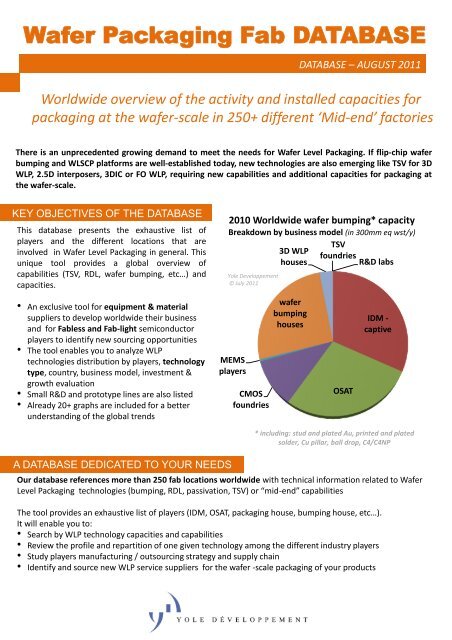
2010 Worldwide wafer bumping* capacity<br />
Breakdown by business model (in 300mm eq wst/y)<br />
TSV<br />
3D WLP<br />
foundries<br />
houses<br />
R&D labs<br />
Yole Developpement<br />
© July 2011<br />
MEMS<br />
players<br />
CMOS<br />
foundries<br />
wafer<br />
bumping<br />
houses<br />
OSAT<br />
IDM -<br />
captive<br />
A <strong>DATABASE</strong> DEDICATED TO YOUR NEEDS<br />
* including: stud and plated Au, printed and plated<br />
solder, Cu pillar, ball drop, C4/C4NP<br />
Our database references more than 250 fab locations worldwide with technical information related to <strong>Wafer</strong><br />
Level <strong>Packaging</strong> technologies (bumping, RDL, passivation, TSV) or “mid-end” capabilities<br />
The tool provides an exhaustive list of players (IDM, OSAT, packaging house, bumping house, etc…).<br />
It will enable you to:<br />
• Search by WLP technology capacities and capabilities<br />
• Review the profile and repartition of one given technology among the different industry players<br />
• Study players manufacturing / outsourcing strategy and supply chain<br />
• Identify and source new WLP service suppliers for the wafer -scale packaging of your products
Content of the database<br />
This database lists the following information:<br />
• General information:<br />
‐ <strong>Fab</strong> location<br />
‐ <strong>Fab</strong> function (Front-end, Back-end, etc…)<br />
‐ Main customer, JV, partnership<br />
• Details about technology:<br />
‐ TSV<br />
‐ RDL and passivation<br />
‐ Bumping technologies (plating, printing, …)<br />
‐ Stacking technologies (W2W, C2W)<br />
• Technology platforms available by location:<br />
‐ WLCSP<br />
‐ FO-WLP<br />
‐ Flip-chip wafer bumping (Au, solder, Cu,<br />
etc…)<br />
‐ 3D-WLCSP<br />
‐ 3DIC<br />
‐ Interposers<br />
‐ <strong>Wafer</strong> Level Optic<br />
• Capacities information (in 300mm eq wf/year):<br />
‐ <strong>Wafer</strong> diameter (4”/6”/8”/12”/panel)<br />
‐ <strong>Wafer</strong> type (Si, GaAs, etc…)<br />
‐ Capacities by platforms<br />
‐ Capacities by bumping technologies<br />
‐ Others capabilities: thin wafer handling,<br />
wafer bonding, …<br />
• Business model & region:<br />
‐ Breakdown by business models<br />
‐ Breakdown by regions<br />
Companies listed in the database<br />
Our database references over 150 companies (IDMs, OSAT, foundries, MEMS, R&D Lab,<br />
etc…) and their 250 + wafer fab locations worldwide<br />
<strong>Wafer</strong> packaging houses:<br />
- Xintec<br />
- China WLCSP<br />
- Nemotek<br />
- OptoPac<br />
- …<br />
R&D Lab & prototype lines:<br />
- CEA LETI<br />
- IMEC<br />
- RTI<br />
- …<br />
MEMS IDM/foundries:<br />
- Silex<br />
- Dalsa<br />
- APM<br />
- …<br />
TSV foundries:<br />
- ALLVia<br />
- EPWorks<br />
- …<br />
<strong>Wafer</strong><br />
<strong>Packaging</strong> <strong>Fab</strong>s<br />
Database<br />
IC manufacturers (IDM):<br />
- Texas Instruments<br />
- STMicroelectronics<br />
- Samsung<br />
- …<br />
<strong>Wafer</strong> bumping houses:<br />
- NEPES<br />
- ChipBond<br />
- FCI<br />
- …<br />
OSAT:<br />
- ASE<br />
- SPIL<br />
- STATSChipPac<br />
- …<br />
CMOS foundries:<br />
- TSMC<br />
- Globalfoundries<br />
- UMC<br />
- …
SAMPLE OF THE CONTENT<br />
This first exhaustive database of 250+ factories with capabilities and capacities for <strong>Wafer</strong><br />
Level <strong>Packaging</strong> applications (Flip Chip wafer bumping, WL CSP, 3D WLP, 3DIC with TSV, 3D<br />
interposers, FO-WLP). Below a partial screen shot of its content.<br />
Capacities (in 300mm eq wf) per platforms<br />
<strong>Wafer</strong> bumping capacities (in 300mm eq wf)
WORLDWIDE MAP OF THE WAFER PACKAGING FABS<br />
250+ wafer fabs with ‘Mid-end’ capabilities worldwide<br />
WHO SHOULD BUY THIS <strong>DATABASE</strong>?<br />
• Equipment & Material suppliers<br />
– Identify key WLP players and locations<br />
worldwide with detailed quantitative and<br />
qualitative information about their installed<br />
capacities for wafer-level-packaging in the Midend<br />
– Screen market penetration status of one<br />
particular technology (e.g. TSV, copper pillar<br />
bumping, gold bumping, RDL, etc…) worldwide<br />
and understand who are their key users<br />
• IDM, fabless and fab-light players<br />
– Oversee supplier subcontractors capabilities and<br />
capacities per WLP technology.<br />
– Benchmark several different subcontractors<br />
– Identify new sourcing strategies<br />
• Small IDM or niche market IDM<br />
– Identify prototype lines for WLP<br />
worldwide<br />
– Identify small fabs capable of handling<br />
very specific wafer-level-packaging<br />
schemes (e.g. with exotic materials, 4’’<br />
small wafer diameter, etc…)<br />
• OSAT, foundries, packaging and bumping<br />
house<br />
– Get an exhaustive list of competitors<br />
or potential partners in your field<br />
– Evaluate global WLP capacities by<br />
technologies, regions, business<br />
models<br />
– Information about key customers’<br />
internal installed capacities in the Midend<br />
BIO OF THE AUTHOR<br />
Christophe Zinck, PhD joined Yole Developpement after several positions in the wafer fab and<br />
packaging environment of CE A-Leti, ST and TriQuint Semiconductor, where he has developed<br />
WLP & flip-chip technology for S AW duplexers. He is now project manager for Advanced<br />
<strong>Packaging</strong>, WLP & 3D system Integration and RF devices. He authored and co-authored 15+<br />
publications and is currently holding 3 US patents.
ORDER FORM<br />
PLEASE ENTER MY ORDER OF " WAFER PACKAGING FAB <strong>DATABASE</strong> 2011” IN:<br />
Corporate license: EURO 5,990*<br />
Single user license: EURO 3,990*<br />
*For price in dollars please use the day’s exchange rate *All products are delivered electronically at payment reception *For French customer, add 19,6 % for VAT<br />
SHIP TO<br />
Name (Mr/Ms/Dr/Pr):<br />
......................................................................................<br />
Job Title:<br />
......................................................................................<br />
Company:<br />
......................................................................................<br />
Address:<br />
......................................................................................<br />
City:<br />
State:<br />
......................................................................................<br />
Postcode/Zip:<br />
......................................................................................<br />
Country*:<br />
......................................................................................<br />
*VAT ID Number for EU members:<br />
......................................................................................<br />
Tel:<br />
......................................................................................<br />
Email:<br />
.....................................................................................<br />
Date:<br />
I hereby accept Yole’s Terms and Conditions of Sale (1)<br />
.......................................................................................<br />
Signature :<br />
......................................................................................<br />
BILLING CONTACT<br />
ABOUT YOLE DEVELOPPEMENT<br />
PAYMENT<br />
On line on Yole website:<br />
http://www.i-micronews.com/reports/<br />
Credit Card:<br />
Visa Mastercard Amex<br />
Name of the Card Holder:<br />
Credit Card Number:<br />
Card Verification Value (3 last digits except AMEX: 4 last digits) :<br />
Expiration date:<br />
By bank transfer:<br />
BANK INFO: HSBC, 1 place de la Bourse, F-69002 Lyon, France,<br />
Bank code : 30056, Branch code : 00170<br />
Account No : 0170 200 1565 87,<br />
SWIFT or BIC code : CCFRFRPP,<br />
IBAN : FR76 3005 6001 7001 7020 0156 587<br />
Return order by:<br />
• FAX: +33 (0)472 83 01 83<br />
• MAIL: YOLE DEVELOPPEMENT, le Quartz,<br />
75 Cours Emile Zola, F - 69100 Lyon<br />
Contact:<br />
David Jourdan, jourdan@yole.fr, Tel: +33 (0)472 83 01 90<br />
1) Our Terms and Conditions of Sale are available www.yole.fr/Terms_and_Conditions_of_Sale.asp.<br />
The present document is valid 12 months after its publication date: 1 st August 2011.<br />
First Name: .................................................................. Last Name: ............................................................................<br />
Email:............................................................................ Phone:.....................................................................................<br />
Beginning in 1998 with Yole Développement, we have grown to become a group of companies providing market research, technology analysis, strategy<br />
consulting, media in addition to finance services. With a solid focus on emerging applications using silicon and/or micro manufacturing Yole<br />
Développement group has expanded to include more than 40 associates worldwide covering MEMS and microfluidics, Advanced <strong>Packaging</strong>, Compound<br />
Semiconductors, Power Electronics, LED, and Photovoltaic. The group supports companies, investors and R&D organizations worldwide to help them<br />
understand markets and follow technology trends to develop their business.<br />
CONSULTING<br />
• Market data, market research and<br />
marketing analysis<br />
• Technology analysis<br />
• Reverse engineering and reverse<br />
costing<br />
• Strategy consulting<br />
• Corporate Finance Advisory (M&A and<br />
fund raising)<br />
REPORTS<br />
• Collection of market & technology<br />
reports<br />
• Players & market databases<br />
• Manufacturing cost simulation<br />
tools<br />
• Component reverse engineering &<br />
costing analysis<br />
MEDIA<br />
• Critical news, Bi-weekly: <strong>Micronews</strong>, the magazine<br />
• In-depth analysis & Quarterly Technology Magazines:<br />
• MEMS Trends– 3D <strong>Packaging</strong> – PV Manufacturing -<br />
Efficien’Si<br />
• Online disruptive technologies website: www.imicronews.com<br />
• Exclusive Webcasts<br />
• Live event with Market Briefings
TERMS AND CONDITIONS OF SALES


