

Fan-in WLCSP matures, what's next? IMT on the role ... - I-Micronews
Fan-in WLCSP matures, what's next? IMT on the role ... - I-Micronews
Fan-in WLCSP matures, what's next? IMT on the role ... - I-Micronews

You also want an ePaper? Increase the reach of your titles
YUMPU automatically turns print PDFs into web optimized ePapers that Google loves.
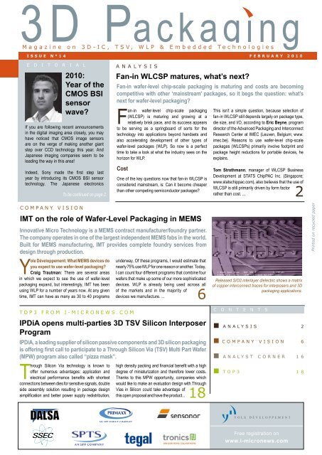
M a g a z i n e o n 3 D - I C , T S V , W L P & E m b e d d e d T e c h n o l o g i e s<br />
I S S U E N ° 1 4 F E B R U A R Y 2 0 1 0<br />
E D I T O R I A L A N A L Y S I S<br />
2010:<br />
Year of <strong>the</strong><br />
CMOS BSI<br />
sensor<br />
wave?<br />
If you are follow<str<strong>on</strong>g>in</str<strong>on</strong>g>g recent announcements<br />
<str<strong>on</strong>g>in</str<strong>on</strong>g> <strong>the</strong> digital imag<str<strong>on</strong>g>in</str<strong>on</strong>g>g area closely, you may<br />
have noticed that CMOS image sensors<br />
are <strong>on</strong> <strong>the</strong> verge of mak<str<strong>on</strong>g>in</str<strong>on</strong>g>g ano<strong>the</strong>r giant<br />
step over CCD technology this year. And<br />
Japanese imag<str<strong>on</strong>g>in</str<strong>on</strong>g>g companies seem to be<br />
lead<str<strong>on</strong>g>in</str<strong>on</strong>g>g <strong>the</strong> way <str<strong>on</strong>g>in</str<strong>on</strong>g> this area!<br />
Indeed, S<strong>on</strong>y made <strong>the</strong> first step last<br />
year by <str<strong>on</strong>g>in</str<strong>on</strong>g>troduc<str<strong>on</strong>g>in</str<strong>on</strong>g>g its CMOS BSI sensor<br />
technology. The Japanese electr<strong>on</strong>ics<br />
To be c<strong>on</strong>t<str<strong>on</strong>g>in</str<strong>on</strong>g>ued <strong>on</strong> page 2.<br />
<str<strong>on</strong>g>Fan</str<strong>on</strong>g>-<str<strong>on</strong>g>in</str<strong>on</strong>g> <str<strong>on</strong>g>WLCSP</str<strong>on</strong>g> <str<strong>on</strong>g>matures</str<strong>on</strong>g>, what’s <str<strong>on</strong>g>next</str<strong>on</strong>g>?<br />
<str<strong>on</strong>g>Fan</str<strong>on</strong>g>-<str<strong>on</strong>g>in</str<strong>on</strong>g> wafer-level chip-scale packag<str<strong>on</strong>g>in</str<strong>on</strong>g>g is matur<str<strong>on</strong>g>in</str<strong>on</strong>g>g and costs are becom<str<strong>on</strong>g>in</str<strong>on</strong>g>g<br />
competitive with o<strong>the</strong>r ‘ma<str<strong>on</strong>g>in</str<strong>on</strong>g>stream’ packages, so it begs <strong>the</strong> questi<strong>on</strong>: what’s<br />
<str<strong>on</strong>g>next</str<strong>on</strong>g> for wafer-level packag<str<strong>on</strong>g>in</str<strong>on</strong>g>g?<br />
<str<strong>on</strong>g>Fan</str<strong>on</strong>g>-<str<strong>on</strong>g>in</str<strong>on</strong>g> wafer-level chip-scale packag<str<strong>on</strong>g>in</str<strong>on</strong>g>g<br />
(<str<strong>on</strong>g>WLCSP</str<strong>on</strong>g>) is matur<str<strong>on</strong>g>in</str<strong>on</strong>g>g and grow<str<strong>on</strong>g>in</str<strong>on</strong>g>g at a<br />
relatively brisk pace, and its success appears<br />
to be serv<str<strong>on</strong>g>in</str<strong>on</strong>g>g as a spr<str<strong>on</strong>g>in</str<strong>on</strong>g>gboard of sorts for <strong>the</strong><br />
technology <str<strong>on</strong>g>in</str<strong>on</strong>g>to applicati<strong>on</strong>s bey<strong>on</strong>d handsets and<br />
also accelerat<str<strong>on</strong>g>in</str<strong>on</strong>g>g development of o<strong>the</strong>r types of<br />
wafer-level packages (WLP). So now is a perfect<br />
time to take a look at what <strong>the</strong> <str<strong>on</strong>g>in</str<strong>on</strong>g>dustry sees <strong>on</strong> <strong>the</strong><br />
horiz<strong>on</strong> for WLP.<br />
Cost<br />
One of <strong>the</strong> key questi<strong>on</strong>s now that fan-<str<strong>on</strong>g>in</str<strong>on</strong>g> <str<strong>on</strong>g>WLCSP</str<strong>on</strong>g> is<br />
c<strong>on</strong>sidered ma<str<strong>on</strong>g>in</str<strong>on</strong>g>stream, is: Can it become cheaper<br />
than o<strong>the</strong>r compet<str<strong>on</strong>g>in</str<strong>on</strong>g>g semic<strong>on</strong>ductor packages?<br />
This isn’t a simple questi<strong>on</strong>, because selecti<strong>on</strong> of<br />
fan-<str<strong>on</strong>g>in</str<strong>on</strong>g> <str<strong>on</strong>g>WLCSP</str<strong>on</strong>g> still depends largely <strong>on</strong> package type,<br />
die size, and I/O, accord<str<strong>on</strong>g>in</str<strong>on</strong>g>g to Eric Beyne, program<br />
director of <strong>the</strong> Advanced Packag<str<strong>on</strong>g>in</str<strong>on</strong>g>g and Interc<strong>on</strong>nect<br />
Research Center at IMEC (Leuven, Belgium; www.<br />
imec.be). Reas<strong>on</strong>s to use wafer-level chip-scale<br />
packages (<str<strong>on</strong>g>WLCSP</str<strong>on</strong>g>s) primarily <str<strong>on</strong>g>in</str<strong>on</strong>g>volve footpr<str<strong>on</strong>g>in</str<strong>on</strong>g>t and<br />
package height reducti<strong>on</strong>s for portable devices, he<br />
expla<str<strong>on</strong>g>in</str<strong>on</strong>g>s.<br />
Tom Strothmann, manager of <str<strong>on</strong>g>WLCSP</str<strong>on</strong>g> Bus<str<strong>on</strong>g>in</str<strong>on</strong>g>ess<br />
Development at STATS ChipPAC Inc. (S<str<strong>on</strong>g>in</str<strong>on</strong>g>gapore;<br />
www.statschippac.com), also believes that <strong>the</strong> use of<br />
<str<strong>on</strong>g>WLCSP</str<strong>on</strong>g> is still primarily driven by form factor<br />
ra<strong>the</strong>r than cost. ...<br />
2<br />
C O M P A N Y V I S I O N<br />
<str<strong>on</strong>g>IMT</str<strong>on</strong>g> <strong>on</strong> <strong>the</strong> <strong>role</strong> of Wafer-Level Packag<str<strong>on</strong>g>in</str<strong>on</strong>g>g <str<strong>on</strong>g>in</str<strong>on</strong>g> MEMS<br />
Innovative Micro Technology is a MEMS c<strong>on</strong>tract manufacturer/foundry partner.<br />
The company operates <str<strong>on</strong>g>in</str<strong>on</strong>g> <strong>on</strong>e of <strong>the</strong> largest <str<strong>on</strong>g>in</str<strong>on</strong>g>dependent MEMS fabs <str<strong>on</strong>g>in</str<strong>on</strong>g> <strong>the</strong> world.<br />
Built for MEMS manufactur<str<strong>on</strong>g>in</str<strong>on</strong>g>g, <str<strong>on</strong>g>IMT</str<strong>on</strong>g> provides complete foundry services from<br />
design through producti<strong>on</strong>.<br />
Yole Développement: What MEMS devices do<br />
you expect to use wafer-level packag<str<strong>on</strong>g>in</str<strong>on</strong>g>g?<br />
Craig Trautman: There are several areas<br />
<str<strong>on</strong>g>in</str<strong>on</strong>g> which we expect to see <strong>the</strong> use of wafer-level<br />
packag<str<strong>on</strong>g>in</str<strong>on</strong>g>g expand, but <str<strong>on</strong>g>in</str<strong>on</strong>g>terest<str<strong>on</strong>g>in</str<strong>on</strong>g>gly, <str<strong>on</strong>g>IMT</str<strong>on</strong>g> has been<br />
us<str<strong>on</strong>g>in</str<strong>on</strong>g>g WLP for a number of years now. At any given<br />
time, <str<strong>on</strong>g>IMT</str<strong>on</strong>g> can have as many as 30 to 40 programs<br />
T O P 3 F R O M I - M I C R O N E W S . C O M<br />
Through Silic<strong>on</strong> Via technology is known to<br />
offer numerous advantages: applicati<strong>on</strong> and<br />
electrical performance benefits with shortest<br />
c<strong>on</strong>necti<strong>on</strong>s between dies for sensitive signals, double<br />
side assembly soluti<strong>on</strong> result<str<strong>on</strong>g>in</str<strong>on</strong>g>g <str<strong>on</strong>g>in</str<strong>on</strong>g> package design<br />
simplificati<strong>on</strong> and better power supply redistributi<strong>on</strong>,<br />
underway. Of <strong>the</strong>se programs, I would estimate that<br />
nearly 75% use WLP for <strong>on</strong>e reas<strong>on</strong> or ano<strong>the</strong>r. Today,<br />
I can count four different programs that comb<str<strong>on</strong>g>in</str<strong>on</strong>g>e four<br />
wafers that make up some of our more sophisticated<br />
devices. WLP is already be<str<strong>on</strong>g>in</str<strong>on</strong>g>g used across all<br />
of <strong>the</strong> markets and <str<strong>on</strong>g>in</str<strong>on</strong>g> <strong>the</strong> majority of<br />
devices we manufacture. ...<br />
IPDiA opens multi-parties 3D TSV Silic<strong>on</strong> Interposer<br />
Program<br />
IPDiA, a lead<str<strong>on</strong>g>in</str<strong>on</strong>g>g supplier of silic<strong>on</strong> passive comp<strong>on</strong>ents and 3D silic<strong>on</strong> packag<str<strong>on</strong>g>in</str<strong>on</strong>g>g<br />
is offer<str<strong>on</strong>g>in</str<strong>on</strong>g>g first call to participate to a Through Silic<strong>on</strong> Via (TSV) Multi Part Wafer<br />
(MPW) program also called “pizza mask”.<br />
6<br />
high density pack<str<strong>on</strong>g>in</str<strong>on</strong>g>g and f<str<strong>on</strong>g>in</str<strong>on</strong>g>ancial benefit with a high<br />
degree of m<str<strong>on</strong>g>in</str<strong>on</strong>g>iaturizati<strong>on</strong> and <strong>the</strong>refore lower costs.<br />
Thanks to this MPW opportunity, companies which<br />
would like to make an evaluati<strong>on</strong> design with Through<br />
Vias <str<strong>on</strong>g>in</str<strong>on</strong>g> Silic<strong>on</strong> could take advantage of<br />
this open proposal and have <strong>the</strong> product...<br />
18<br />
Released SiO2 <str<strong>on</strong>g>in</str<strong>on</strong>g>terlayer dielectric shows a matrix<br />
of copper <str<strong>on</strong>g>in</str<strong>on</strong>g>terc<strong>on</strong>nect traces for <str<strong>on</strong>g>in</str<strong>on</strong>g>terposers and 3D<br />
packag<str<strong>on</strong>g>in</str<strong>on</strong>g>g applicati<strong>on</strong>s.<br />
C O N T E N T S<br />
A N A L Y S I S 2<br />
C O M P A N Y V I S I O N 6<br />
A N A L Y S T C O R N E R 1 6<br />
T O P 3 1 8<br />
Pr<str<strong>on</strong>g>in</str<strong>on</strong>g>ted <strong>on</strong> recycled paper<br />
Free registrati<strong>on</strong> <strong>on</strong><br />
www.i-micr<strong>on</strong>ews.com
F E B R U A R Y 2 0 1 0 i s s u e n ° 1 4<br />
N e w s l e t t e r o n 3 D I C , T S V , W L P & E m b e d d e d T e c h n o l o g i e s<br />
E D I T O R I A L<br />
giant is now mass produc<str<strong>on</strong>g>in</str<strong>on</strong>g>g <strong>the</strong> CMOS<br />
BSI sensor <str<strong>on</strong>g>in</str<strong>on</strong>g> its newest video camcorders<br />
and digital still cameras. But S<strong>on</strong>y is not<br />
an isolated case as <str<strong>on</strong>g>in</str<strong>on</strong>g> early January, many<br />
o<strong>the</strong>r announcements have followed and not<br />
<strong>on</strong>ly Casio but also Nik<strong>on</strong>, Ricoh, Samsung,<br />
JVC and Fujifilm all separately announced<br />
<strong>the</strong>ir first digital camera products us<str<strong>on</strong>g>in</str<strong>on</strong>g>g a<br />
CMOS sensor… based <strong>on</strong> BSI “Backside<br />
illum<str<strong>on</strong>g>in</str<strong>on</strong>g>ati<strong>on</strong>” technology!<br />
So, a lot of <str<strong>on</strong>g>in</str<strong>on</strong>g>terest<str<strong>on</strong>g>in</str<strong>on</strong>g>g announcements <str<strong>on</strong>g>in</str<strong>on</strong>g> <strong>the</strong><br />
high-end imag<str<strong>on</strong>g>in</str<strong>on</strong>g>g market have happened<br />
early this year. But <strong>the</strong> low-end image sensor<br />
market will not stand by and watch as we<br />
believe that CMOS BSI technology will also<br />
appear <str<strong>on</strong>g>in</str<strong>on</strong>g>to different smart-ph<strong>on</strong>e camera<br />
products later this year. Omnivisi<strong>on</strong> is ready<br />
and currently sampl<str<strong>on</strong>g>in</str<strong>on</strong>g>g its sec<strong>on</strong>d generati<strong>on</strong><br />
BSI image sensor. Apt<str<strong>on</strong>g>in</str<strong>on</strong>g>a Imag<str<strong>on</strong>g>in</str<strong>on</strong>g>g, Toshiba,<br />
Samsung and STMicro are also <str<strong>on</strong>g>in</str<strong>on</strong>g> <strong>the</strong><br />
start<str<strong>on</strong>g>in</str<strong>on</strong>g>g-blocks.<br />
Yole is follow<str<strong>on</strong>g>in</str<strong>on</strong>g>g <strong>the</strong> CMOS image sensor<br />
market very closely for several years now. We<br />
are very pleased to announce <strong>the</strong> imm<str<strong>on</strong>g>in</str<strong>on</strong>g>ent<br />
release of our all new market study <str<strong>on</strong>g>in</str<strong>on</strong>g> this<br />
area. This report will of course provide <strong>the</strong><br />
key technical <str<strong>on</strong>g>in</str<strong>on</strong>g>sights about <strong>the</strong> very latest<br />
technology trends such as BSI, Wafer Level<br />
Cameras, image stabilizati<strong>on</strong> and auto-focus<br />
technologies that are under development for<br />
<strong>the</strong> camera module market!<br />
A N A L Y S I S<br />
<str<strong>on</strong>g>Fan</str<strong>on</strong>g>-<str<strong>on</strong>g>in</str<strong>on</strong>g> <str<strong>on</strong>g>WLCSP</str<strong>on</strong>g> <str<strong>on</strong>g>matures</str<strong>on</strong>g>, what’s <str<strong>on</strong>g>next</str<strong>on</strong>g>?<br />
From page 1<br />
QFN packages are <strong>the</strong> most competitive with<br />
<str<strong>on</strong>g>WLCSP</str<strong>on</strong>g> <str<strong>on</strong>g>in</str<strong>on</strong>g> <strong>the</strong> market space requir<str<strong>on</strong>g>in</str<strong>on</strong>g>g reduced<br />
form factor, he says. <str<strong>on</strong>g>WLCSP</str<strong>on</strong>g> cost is competitive<br />
with QFN today <str<strong>on</strong>g>in</str<strong>on</strong>g> small die sizes with low I/O<br />
counts and less expensive than QFN as <strong>the</strong> I/O<br />
count <str<strong>on</strong>g>in</str<strong>on</strong>g>creases. <str<strong>on</strong>g>Fan</str<strong>on</strong>g>-<str<strong>on</strong>g>in</str<strong>on</strong>g> <str<strong>on</strong>g>WLCSP</str<strong>on</strong>g> is expected to<br />
become less expensive than QFN packages <str<strong>on</strong>g>in</str<strong>on</strong>g> all<br />
die sizes as <str<strong>on</strong>g>WLCSP</str<strong>on</strong>g> volume <str<strong>on</strong>g>in</str<strong>on</strong>g>creases.<br />
<str<strong>on</strong>g>Fan</str<strong>on</strong>g>-<str<strong>on</strong>g>in</str<strong>on</strong>g> <str<strong>on</strong>g>WLCSP</str<strong>on</strong>g>s c<strong>on</strong>t<str<strong>on</strong>g>in</str<strong>on</strong>g>ue to have <strong>the</strong> highest<br />
year-over-year adopti<strong>on</strong> rate of all semic<strong>on</strong>ductor<br />
packages, says Ted Tessier, chief technical<br />
officer of FlipChip Internati<strong>on</strong>al (Phoenix, Ariz.;<br />
www.flipchip.com), thanks to <strong>the</strong>ir m<str<strong>on</strong>g>in</str<strong>on</strong>g>imalist form<br />
factor at an attractive price po<str<strong>on</strong>g>in</str<strong>on</strong>g>t. “Most of <strong>the</strong><br />
high-volume suppliers of <str<strong>on</strong>g>WLCSP</str<strong>on</strong>g>s are driv<str<strong>on</strong>g>in</str<strong>on</strong>g>g<br />
an aggressive cost-reducti<strong>on</strong> roadmap and, as a<br />
result, <strong>the</strong> pric<str<strong>on</strong>g>in</str<strong>on</strong>g>g has dropped gradually. But after<br />
10 years of high-volume usage, c<strong>on</strong>t<str<strong>on</strong>g>in</str<strong>on</strong>g>ued price<br />
reducti<strong>on</strong> is becom<str<strong>on</strong>g>in</str<strong>on</strong>g>g <str<strong>on</strong>g>in</str<strong>on</strong>g>creas<str<strong>on</strong>g>in</str<strong>on</strong>g>gly difficult and<br />
level<str<strong>on</strong>g>in</str<strong>on</strong>g>g off,” he adds.<br />
lead<str<strong>on</strong>g>in</str<strong>on</strong>g>g semic<strong>on</strong>ductor package because many<br />
applicati<strong>on</strong>s where space isn’t critical d<strong>on</strong>’t have<br />
str<strong>on</strong>g drivers to migrate to <str<strong>on</strong>g>WLCSP</str<strong>on</strong>g>.<br />
“It’s <strong>on</strong>e of <strong>the</strong> faster-grow<str<strong>on</strong>g>in</str<strong>on</strong>g>g packages, al<strong>on</strong>g with<br />
QFN, but both have a way to go to catch up with <strong>the</strong><br />
more established packages, which will c<strong>on</strong>t<str<strong>on</strong>g>in</str<strong>on</strong>g>ue to<br />
grow at a slower pace,” says Stepniak.<br />
Beyne notes that <strong>the</strong> majority of packages are<br />
still lead-frame-based soluti<strong>on</strong>s, but expects <strong>the</strong><br />
compound annual growth rate (CAGR) of <str<strong>on</strong>g>WLCSP</str<strong>on</strong>g>s<br />
will be much greater.<br />
Expand<str<strong>on</strong>g>in</str<strong>on</strong>g>g to more apps?<br />
Ano<strong>the</strong>r big questi<strong>on</strong> is: Will <strong>the</strong> success of fan<str<strong>on</strong>g>in</str<strong>on</strong>g><br />
<str<strong>on</strong>g>WLCSP</str<strong>on</strong>g> <str<strong>on</strong>g>in</str<strong>on</strong>g> mobile applicati<strong>on</strong>s, first <str<strong>on</strong>g>in</str<strong>on</strong>g>tegrated<br />
for size/m<str<strong>on</strong>g>in</str<strong>on</strong>g>iaturizati<strong>on</strong> drivers, allow for its wide<br />
adopti<strong>on</strong> by o<strong>the</strong>r c<strong>on</strong>sumer applicati<strong>on</strong>s?<br />
“… QFN packages are <strong>the</strong> most competitive with <str<strong>on</strong>g>WLCSP</str<strong>on</strong>g> <str<strong>on</strong>g>in</str<strong>on</strong>g> <strong>the</strong><br />
market space requir<str<strong>on</strong>g>in</str<strong>on</strong>g>g reduced form factor …”, accord<str<strong>on</strong>g>in</str<strong>on</strong>g>g to Tom<br />
Strothmann, STATS ChipPAC Inc.<br />
Jérôme Bar<strong>on</strong><br />
Technology & Market Analyst & Editor<br />
bar<strong>on</strong>@yole.fr<br />
E V E N T S<br />
• DATE 2010 - Design, Automati<strong>on</strong> &<br />
Test <str<strong>on</strong>g>in</str<strong>on</strong>g> Europe<br />
March 8-9, Dresden, Germany<br />
• IMAPS 2010 : 6th Internati<strong>on</strong>al<br />
C<strong>on</strong>ference and Exhibiti<strong>on</strong> <strong>on</strong> Device<br />
Packag<str<strong>on</strong>g>in</str<strong>on</strong>g>g,<br />
March 9- 11, Scottsdale, AZ, USA<br />
• Image Sensors Europe,<br />
March 23-25, L<strong>on</strong>d<strong>on</strong>, UK<br />
Issue sp<strong>on</strong>sored by:<br />
While fan-<str<strong>on</strong>g>in</str<strong>on</strong>g> is becom<str<strong>on</strong>g>in</str<strong>on</strong>g>g cheaper, so are compet<str<strong>on</strong>g>in</str<strong>on</strong>g>g<br />
semic<strong>on</strong>ductor packages, po<str<strong>on</strong>g>in</str<strong>on</strong>g>ts out David<br />
Stepniak, manager of WCSP and 3D packag<str<strong>on</strong>g>in</str<strong>on</strong>g>g at<br />
Texas Instruments (Dallas, Texas; www.ti.com). He<br />
doesn’t anticipate a change <str<strong>on</strong>g>in</str<strong>on</strong>g> packag<str<strong>on</strong>g>in</str<strong>on</strong>g>g strategy<br />
between fan-<str<strong>on</strong>g>in</str<strong>on</strong>g> <str<strong>on</strong>g>WLCSP</str<strong>on</strong>g> and o<strong>the</strong>r packages based<br />
<strong>on</strong> relative price or cost changes.<br />
And <str<strong>on</strong>g>in</str<strong>on</strong>g> many cases, David Kress, director of<br />
Technical Market<str<strong>on</strong>g>in</str<strong>on</strong>g>g at Analog Devices Inc.<br />
(Norwood, Mass.; www.analog.com), says that<br />
<str<strong>on</strong>g>WLCSP</str<strong>on</strong>g> has already become <strong>the</strong> least expensive<br />
package.<br />
Lead<str<strong>on</strong>g>in</str<strong>on</strong>g>g package?<br />
Is fan-<str<strong>on</strong>g>in</str<strong>on</strong>g> <str<strong>on</strong>g>WLCSP</str<strong>on</strong>g> emerg<str<strong>on</strong>g>in</str<strong>on</strong>g>g as <strong>the</strong> overall lead<str<strong>on</strong>g>in</str<strong>on</strong>g>g<br />
semic<strong>on</strong>ductor package? With so many packages<br />
out <strong>the</strong>re to choose from, it’s hardly surpris<str<strong>on</strong>g>in</str<strong>on</strong>g>g that<br />
op<str<strong>on</strong>g>in</str<strong>on</strong>g>i<strong>on</strong>s vary a little.<br />
<str<strong>on</strong>g>Fan</str<strong>on</strong>g>-<str<strong>on</strong>g>in</str<strong>on</strong>g> <str<strong>on</strong>g>WLCSP</str<strong>on</strong>g> has <strong>the</strong> highest growth rate of<br />
all ma<str<strong>on</strong>g>in</str<strong>on</strong>g>stream semic<strong>on</strong>ductor packages, says<br />
Strothmann, but it’s start<str<strong>on</strong>g>in</str<strong>on</strong>g>g from a smaller base<br />
than o<strong>the</strong>r package technologies. He expects it<br />
will become <strong>the</strong> dom<str<strong>on</strong>g>in</str<strong>on</strong>g>ant package <str<strong>on</strong>g>in</str<strong>on</strong>g> handheld<br />
products where a reduced form factor is critical,<br />
but feels it’s unlikely to become <strong>the</strong> overall<br />
“The <str<strong>on</strong>g>in</str<strong>on</strong>g>dustry-wide high-volume <str<strong>on</strong>g>in</str<strong>on</strong>g>frastructure that<br />
was put <str<strong>on</strong>g>in</str<strong>on</strong>g>to place for <strong>the</strong> fabricati<strong>on</strong>, back-end die<br />
process<str<strong>on</strong>g>in</str<strong>on</strong>g>g, and surface mount technology (SMT)<br />
usage of <str<strong>on</strong>g>WLCSP</str<strong>on</strong>g>s to support <strong>the</strong> ultrahigh-volume<br />
requirements of mobile applicati<strong>on</strong>s is def<str<strong>on</strong>g>in</str<strong>on</strong>g>itely<br />
provid<str<strong>on</strong>g>in</str<strong>on</strong>g>g a robust base from which <strong>the</strong> proliferati<strong>on</strong><br />
of <str<strong>on</strong>g>WLCSP</str<strong>on</strong>g>s is spr<str<strong>on</strong>g>in</str<strong>on</strong>g>g<str<strong>on</strong>g>in</str<strong>on</strong>g>g <str<strong>on</strong>g>in</str<strong>on</strong>g>to o<strong>the</strong>r applicati<strong>on</strong><br />
spaces,” says Tessier. “We’re see<str<strong>on</strong>g>in</str<strong>on</strong>g>g significant<br />
adopti<strong>on</strong> and eng<str<strong>on</strong>g>in</str<strong>on</strong>g>eer<str<strong>on</strong>g>in</str<strong>on</strong>g>g <str<strong>on</strong>g>in</str<strong>on</strong>g>terest <str<strong>on</strong>g>in</str<strong>on</strong>g> automotive,<br />
medical, comput<str<strong>on</strong>g>in</str<strong>on</strong>g>g, and digital photography.<br />
SEM Photomicrograph of a <str<strong>on</strong>g>Fan</str<strong>on</strong>g>-In <str<strong>on</strong>g>WLCSP</str<strong>on</strong>g><br />
embedded <str<strong>on</strong>g>in</str<strong>on</strong>g> a PCB lam<str<strong>on</strong>g>in</str<strong>on</strong>g>ate (Courtesy of FlipChip)<br />
2
F E B R U A R Y 2 0 1 0 i s s u e n ° 1 4<br />
N e w s l e t t e r o n 3 D I C , T S V , W L P & E m b e d d e d T e c h n o l o g i e s<br />
Tessier also believes that <strong>the</strong> requirement for fanout<br />
<str<strong>on</strong>g>WLCSP</str<strong>on</strong>g>s is limited to quite a small number of<br />
higher I/O applicati<strong>on</strong>s that may not be compatible<br />
with <strong>the</strong> pitch limitati<strong>on</strong>s, I/O count or o<strong>the</strong>r<br />
factors associated with fan-<str<strong>on</strong>g>in</str<strong>on</strong>g> <str<strong>on</strong>g>WLCSP</str<strong>on</strong>g>s. “There<br />
is a substantial amount of buzz <str<strong>on</strong>g>in</str<strong>on</strong>g> <strong>the</strong> <str<strong>on</strong>g>in</str<strong>on</strong>g>dustry <str<strong>on</strong>g>in</str<strong>on</strong>g><br />
<strong>the</strong> area of fan-out <str<strong>on</strong>g>WLCSP</str<strong>on</strong>g>s today, but <strong>the</strong>re are<br />
o<strong>the</strong>r packag<str<strong>on</strong>g>in</str<strong>on</strong>g>g opti<strong>on</strong>s with very large <str<strong>on</strong>g>in</str<strong>on</strong>g>stalled<br />
capacities, <str<strong>on</strong>g>in</str<strong>on</strong>g>clud<str<strong>on</strong>g>in</str<strong>on</strong>g>g flip chip BGAs, wireb<strong>on</strong>d<br />
array packag<str<strong>on</strong>g>in</str<strong>on</strong>g>g, etc., which will require fan-out<br />
<str<strong>on</strong>g>WLCSP</str<strong>on</strong>g>s to realize dramatic cost reducti<strong>on</strong>s to<br />
become viable alternatives,” he expla<str<strong>on</strong>g>in</str<strong>on</strong>g>s.<br />
Cross-Secti<strong>on</strong>al View of an Embedded Die <str<strong>on</strong>g>in</str<strong>on</strong>g> Pr<str<strong>on</strong>g>in</str<strong>on</strong>g>ted Wir<str<strong>on</strong>g>in</str<strong>on</strong>g>g Board <str<strong>on</strong>g>Fan</str<strong>on</strong>g>-Out Interc<strong>on</strong>nect<br />
(Courtesy of FlipChip)<br />
Stepniak anticipates research-related items will<br />
be directed more toward 3D, SiP, and MEMStype<br />
packag<str<strong>on</strong>g>in</str<strong>on</strong>g>g. “<str<strong>on</strong>g>Fan</str<strong>on</strong>g>-out WCSP is likely <strong>on</strong>ly an<br />
<str<strong>on</strong>g>in</str<strong>on</strong>g>terim step until 3D is available. <str<strong>on</strong>g>Fan</str<strong>on</strong>g>-<str<strong>on</strong>g>in</str<strong>on</strong>g> WCSP will<br />
c<strong>on</strong>t<str<strong>on</strong>g>in</str<strong>on</strong>g>ue str<strong>on</strong>g with similar research for apply<str<strong>on</strong>g>in</str<strong>on</strong>g>g<br />
to 3D,” he says.<br />
<str<strong>on</strong>g>WLCSP</str<strong>on</strong>g>s are also f<str<strong>on</strong>g>in</str<strong>on</strong>g>d<str<strong>on</strong>g>in</str<strong>on</strong>g>g broader use <str<strong>on</strong>g>in</str<strong>on</strong>g> device<br />
applicati<strong>on</strong>s bey<strong>on</strong>d silic<strong>on</strong> semic<strong>on</strong>ductors and<br />
are start<str<strong>on</strong>g>in</str<strong>on</strong>g>g to be adopted by a broad assortment<br />
of substrate and device technologies, <str<strong>on</strong>g>in</str<strong>on</strong>g>clud<str<strong>on</strong>g>in</str<strong>on</strong>g>g<br />
MEMS, SAW and BAW filters, GaAs RF devices,<br />
etc.”<br />
There are some issues with meet<str<strong>on</strong>g>in</str<strong>on</strong>g>g automotive<br />
requirements. “Automotive and similar low to zero<br />
DPPM requirements are a challenge, because <strong>the</strong><br />
standard <str<strong>on</strong>g>WLCSP</str<strong>on</strong>g> flow doesn’t have a f<str<strong>on</strong>g>in</str<strong>on</strong>g>al package<br />
test,” po<str<strong>on</strong>g>in</str<strong>on</strong>g>ts out Stepniak.<br />
And a key factor pac<str<strong>on</strong>g>in</str<strong>on</strong>g>g <strong>the</strong> adopti<strong>on</strong> rate has been<br />
and will c<strong>on</strong>t<str<strong>on</strong>g>in</str<strong>on</strong>g>ue to be board cost, Strothmann says.<br />
“As f<str<strong>on</strong>g>in</str<strong>on</strong>g>e pitch board costs decl<str<strong>on</strong>g>in</str<strong>on</strong>g>e, <strong>the</strong> adopti<strong>on</strong><br />
rate of <str<strong>on</strong>g>WLCSP</str<strong>on</strong>g> <str<strong>on</strong>g>in</str<strong>on</strong>g> o<strong>the</strong>r c<strong>on</strong>sumer applicati<strong>on</strong>s<br />
will <str<strong>on</strong>g>in</str<strong>on</strong>g>crease. Most c<strong>on</strong>sumer applicati<strong>on</strong>s are<br />
heavily cost-driven and <strong>the</strong> end product will use<br />
<strong>the</strong> least expensive soluti<strong>on</strong> that meets design<br />
requirements. Applicati<strong>on</strong>s that use high-density<br />
PCBs similar to mobile applicati<strong>on</strong>s are f<str<strong>on</strong>g>in</str<strong>on</strong>g>e for<br />
small die, low I/O count. <str<strong>on</strong>g>Fan</str<strong>on</strong>g>-out <str<strong>on</strong>g>WLCSP</str<strong>on</strong>g> will be<br />
more important <str<strong>on</strong>g>in</str<strong>on</strong>g> <strong>the</strong> future than fan-<str<strong>on</strong>g>in</str<strong>on</strong>g> <str<strong>on</strong>g>WLCSP</str<strong>on</strong>g><br />
because it can deliver an I/O footpr<str<strong>on</strong>g>in</str<strong>on</strong>g>t that’s larger<br />
than <strong>the</strong> IC size,” he stresses.<br />
Beyne also believes that fan-out <str<strong>on</strong>g>WLCSP</str<strong>on</strong>g> will be<br />
more important <str<strong>on</strong>g>in</str<strong>on</strong>g> <strong>the</strong> future than fan-<str<strong>on</strong>g>in</str<strong>on</strong>g> <str<strong>on</strong>g>WLCSP</str<strong>on</strong>g>,<br />
because it can deliver an I/O footpr<str<strong>on</strong>g>in</str<strong>on</strong>g>t that’s larger<br />
than <strong>the</strong> IC size.<br />
New directi<strong>on</strong>s for WLP?<br />
Beyne. “<str<strong>on</strong>g>Fan</str<strong>on</strong>g>-out <str<strong>on</strong>g>WLCSP</str<strong>on</strong>g> is <str<strong>on</strong>g>in</str<strong>on</strong>g> <strong>the</strong> early phase of<br />
development. New soluti<strong>on</strong>s are required to allow<br />
for larger die and package size with high reliability.<br />
Significant improvements can still be realized. 3D<br />
stack<str<strong>on</strong>g>in</str<strong>on</strong>g>g isn’t <str<strong>on</strong>g>in</str<strong>on</strong>g> competiti<strong>on</strong> with WLP, but 3D WLP<br />
stacks are also possible.”<br />
There c<strong>on</strong>t<str<strong>on</strong>g>in</str<strong>on</strong>g>ues to be a large amount of eng<str<strong>on</strong>g>in</str<strong>on</strong>g>eer<str<strong>on</strong>g>in</str<strong>on</strong>g>g<br />
activity <str<strong>on</strong>g>in</str<strong>on</strong>g> <strong>the</strong> <str<strong>on</strong>g>in</str<strong>on</strong>g>dustry to push <strong>the</strong> envelope<br />
of <str<strong>on</strong>g>WLCSP</str<strong>on</strong>g> usage to enable larger I/O counts<br />
through f<str<strong>on</strong>g>in</str<strong>on</strong>g>er pitches, improve reliability for given<br />
array sizes, and enable cost reducti<strong>on</strong> through<br />
<str<strong>on</strong>g>WLCSP</str<strong>on</strong>g> process simplificati<strong>on</strong>, notes Tessier.<br />
He anticipates migrati<strong>on</strong> toward 0.3mm-pitch<br />
comp<strong>on</strong>ents, which will require substantial SMT<br />
assembly process improvements and equipment<br />
upgrades. In parallel to this <strong>on</strong>go<str<strong>on</strong>g>in</str<strong>on</strong>g>g activity <str<strong>on</strong>g>in</str<strong>on</strong>g> 2D<br />
<str<strong>on</strong>g>WLCSP</str<strong>on</strong>g> packag<str<strong>on</strong>g>in</str<strong>on</strong>g>g activities, he expects some of<br />
<strong>the</strong> focus will be directed <str<strong>on</strong>g>in</str<strong>on</strong>g>crementally toward 3D<br />
<str<strong>on</strong>g>WLCSP</str<strong>on</strong>g> stack<str<strong>on</strong>g>in</str<strong>on</strong>g>g, etc.<br />
Strothmann expects that c<strong>on</strong>t<str<strong>on</strong>g>in</str<strong>on</strong>g>ued research<br />
will make fan-<str<strong>on</strong>g>in</str<strong>on</strong>g> <str<strong>on</strong>g>WLCSP</str<strong>on</strong>g> more reliable and less<br />
expensive, and fan-<str<strong>on</strong>g>in</str<strong>on</strong>g> <str<strong>on</strong>g>WLCSP</str<strong>on</strong>g> will c<strong>on</strong>t<str<strong>on</strong>g>in</str<strong>on</strong>g>ue to have<br />
cost advantages over competitive technologies.<br />
“The fan-<str<strong>on</strong>g>in</str<strong>on</strong>g> bump pitch will decrease and numbers of<br />
I/Os used <strong>on</strong> fan-<str<strong>on</strong>g>in</str<strong>on</strong>g> packages will <str<strong>on</strong>g>in</str<strong>on</strong>g>crease as new<br />
materials and structures become available,” he<br />
says. “By <strong>the</strong> nature of <strong>the</strong>se technologies many<br />
of <strong>the</strong> <str<strong>on</strong>g>in</str<strong>on</strong>g>novati<strong>on</strong>s developed are <str<strong>on</strong>g>in</str<strong>on</strong>g>terchangeable<br />
between fan-<str<strong>on</strong>g>in</str<strong>on</strong>g>, fan-out, and 3D packag<str<strong>on</strong>g>in</str<strong>on</strong>g>g, so <str<strong>on</strong>g>in</str<strong>on</strong>g><br />
many respects <strong>the</strong> <str<strong>on</strong>g>in</str<strong>on</strong>g>novati<strong>on</strong> expenses are spread<br />
across <strong>the</strong> technologies.”<br />
Silic<strong>on</strong> <str<strong>on</strong>g>in</str<strong>on</strong>g>terposers?<br />
Will we see <strong>the</strong> widespread adopti<strong>on</strong> of silic<strong>on</strong><br />
<str<strong>on</strong>g>in</str<strong>on</strong>g>terposers, and will it c<strong>on</strong>tribute to a higher rate<br />
of fan-<str<strong>on</strong>g>in</str<strong>on</strong>g> <str<strong>on</strong>g>WLCSP</str<strong>on</strong>g> use <str<strong>on</strong>g>in</str<strong>on</strong>g> <strong>the</strong> packag<str<strong>on</strong>g>in</str<strong>on</strong>g>g <str<strong>on</strong>g>in</str<strong>on</strong>g>dustry?<br />
The general c<strong>on</strong>sensus is that it’s not likely any<br />
time so<strong>on</strong> because of limited applicati<strong>on</strong>s and <strong>the</strong><br />
associated high costs.<br />
Will more research and effort be directed toward<br />
mak<str<strong>on</strong>g>in</str<strong>on</strong>g>g cheaper or more reliable fan-<str<strong>on</strong>g>in</str<strong>on</strong>g> <str<strong>on</strong>g>WLCSP</str<strong>on</strong>g>, or<br />
will <strong>the</strong>se <str<strong>on</strong>g>in</str<strong>on</strong>g>novati<strong>on</strong> expenses be diverted to fanout<br />
<str<strong>on</strong>g>WLCSP</str<strong>on</strong>g> or o<strong>the</strong>r WLP technologies such as<br />
3D IC stack<str<strong>on</strong>g>in</str<strong>on</strong>g>g with TSVs or MEMS capp<str<strong>on</strong>g>in</str<strong>on</strong>g>g and<br />
packag<str<strong>on</strong>g>in</str<strong>on</strong>g>g?<br />
“<str<strong>on</strong>g>Fan</str<strong>on</strong>g>-<str<strong>on</strong>g>in</str<strong>on</strong>g> <str<strong>on</strong>g>WLCSP</str<strong>on</strong>g>s are established schemes, and<br />
development is ma<str<strong>on</strong>g>in</str<strong>on</strong>g>ly related to <str<strong>on</strong>g>in</str<strong>on</strong>g>cremental<br />
improvement of materials to obta<str<strong>on</strong>g>in</str<strong>on</strong>g> better <strong>the</strong>rmal<br />
cycl<str<strong>on</strong>g>in</str<strong>on</strong>g>g performance. There is little value <str<strong>on</strong>g>in</str<strong>on</strong>g> scal<str<strong>on</strong>g>in</str<strong>on</strong>g>g<br />
I/O pitch (narrows down <strong>the</strong> applicati<strong>on</strong> space to<br />
special, expensive PCB board technologies),” says<br />
eWLB rec<strong>on</strong>stituated water (Courtesy of STATS ChipPac)<br />
3
F E B R U A R Y 2 0 1 0 i s s u e n ° 1 4<br />
N e w s l e t t e r o n 3 D I C , T S V , W L P & E m b e d d e d T e c h n o l o g i e s<br />
“… Silic<strong>on</strong> <str<strong>on</strong>g>in</str<strong>on</strong>g>terposers are currently s<str<strong>on</strong>g>in</str<strong>on</strong>g>gle-sided relatively<br />
expensive <str<strong>on</strong>g>in</str<strong>on</strong>g>terc<strong>on</strong>necti<strong>on</strong> media compared to o<strong>the</strong>r comparable<br />
density PCB-based technologies …” accord<str<strong>on</strong>g>in</str<strong>on</strong>g>g to Ted Tessier,<br />
FlipChip Internati<strong>on</strong>al<br />
for TCE match<str<strong>on</strong>g>in</str<strong>on</strong>g>g or additi<strong>on</strong>al functi<strong>on</strong>ality <str<strong>on</strong>g>in</str<strong>on</strong>g> <strong>the</strong><br />
form of power rout<str<strong>on</strong>g>in</str<strong>on</strong>g>g and passive comp<strong>on</strong>ents.<br />
O<strong>the</strong>r than <strong>the</strong>se segments, widespread adopti<strong>on</strong><br />
isn’t expected.<br />
<str<strong>on</strong>g>Fan</str<strong>on</strong>g>-<str<strong>on</strong>g>in</str<strong>on</strong>g> WLP market growth<br />
The applicati<strong>on</strong> space is limited to high-end<br />
products for large silic<strong>on</strong> <str<strong>on</strong>g>in</str<strong>on</strong>g>terposers, accord<str<strong>on</strong>g>in</str<strong>on</strong>g>g<br />
to Beyne, like those with <str<strong>on</strong>g>in</str<strong>on</strong>g>tegrated functi<strong>on</strong>alities<br />
such as ESD, RF, power-c<strong>on</strong>versi<strong>on</strong> modules.<br />
“… Silic<strong>on</strong> <str<strong>on</strong>g>in</str<strong>on</strong>g>terposers are currently s<str<strong>on</strong>g>in</str<strong>on</strong>g>glesided<br />
relatively expensive <str<strong>on</strong>g>in</str<strong>on</strong>g>terc<strong>on</strong>necti<strong>on</strong> media<br />
compared to o<strong>the</strong>r comparable density PCB-based<br />
technologies …” accord<str<strong>on</strong>g>in</str<strong>on</strong>g>g to Ted Tessier, FlipChip<br />
Internati<strong>on</strong>al<br />
Tessier doesn’t expect to see widespread<br />
adopti<strong>on</strong> of silic<strong>on</strong> <str<strong>on</strong>g>in</str<strong>on</strong>g>terposers <str<strong>on</strong>g>in</str<strong>on</strong>g> <strong>the</strong> foreseeable<br />
future. “Silic<strong>on</strong> <str<strong>on</strong>g>in</str<strong>on</strong>g>terposers are currently s<str<strong>on</strong>g>in</str<strong>on</strong>g>glesided<br />
relatively expensive <str<strong>on</strong>g>in</str<strong>on</strong>g>terc<strong>on</strong>necti<strong>on</strong> media<br />
compared to o<strong>the</strong>r comparable density PCBbased<br />
technologies,” he expla<str<strong>on</strong>g>in</str<strong>on</strong>g>s. “Although<br />
<strong>the</strong>re may be some niche opportunities for <strong>the</strong>m<br />
<str<strong>on</strong>g>in</str<strong>on</strong>g> high-performance packag<str<strong>on</strong>g>in</str<strong>on</strong>g>g applicati<strong>on</strong>s, <strong>the</strong><br />
costs <str<strong>on</strong>g>in</str<strong>on</strong>g>volved will be prohibitive. There has been<br />
c<strong>on</strong>siderable <str<strong>on</strong>g>in</str<strong>on</strong>g>dustry menti<strong>on</strong> recently <str<strong>on</strong>g>in</str<strong>on</strong>g> <strong>the</strong> area<br />
of TSV-based double-sided silic<strong>on</strong> <str<strong>on</strong>g>in</str<strong>on</strong>g>terposers.<br />
Though such double-sided silic<strong>on</strong> substrates<br />
should provide improved 3D functi<strong>on</strong>al <str<strong>on</strong>g>in</str<strong>on</strong>g>tegrati<strong>on</strong><br />
potential, <strong>the</strong> added costs of z-axis process<str<strong>on</strong>g>in</str<strong>on</strong>g>g will<br />
likely provide significant cost obstacles relative to<br />
o<strong>the</strong>r opti<strong>on</strong>s. If anyth<str<strong>on</strong>g>in</str<strong>on</strong>g>g, silic<strong>on</strong> <str<strong>on</strong>g>in</str<strong>on</strong>g>terposers will<br />
likely c<strong>on</strong>tribute to a higher rate of f<str<strong>on</strong>g>in</str<strong>on</strong>g>e-pitch flip<br />
chip usage at pitches below <strong>the</strong> practical pitches<br />
of lam<str<strong>on</strong>g>in</str<strong>on</strong>g>ate and o<strong>the</strong>r substrate technologies—<br />
typically 100µm pitch or less.”<br />
Widespread adopti<strong>on</strong> will occur <strong>on</strong>ly if <strong>the</strong> 3D<br />
packag<str<strong>on</strong>g>in</str<strong>on</strong>g>g soluti<strong>on</strong>s without an <str<strong>on</strong>g>in</str<strong>on</strong>g>terposer are<br />
found to take l<strong>on</strong>ger time to develop and an <str<strong>on</strong>g>in</str<strong>on</strong>g>terim<br />
soluti<strong>on</strong> is needed, says Stepniak. O<strong>the</strong>rwise, it’s<br />
a cost adder that will be targeted for elim<str<strong>on</strong>g>in</str<strong>on</strong>g>ati<strong>on</strong>.<br />
Kress believes that <str<strong>on</strong>g>in</str<strong>on</strong>g>terposers will be used for<br />
certa<str<strong>on</strong>g>in</str<strong>on</strong>g> applicati<strong>on</strong>s, but aren’t likely to be adopted<br />
across <strong>the</strong> board, and will c<strong>on</strong>tribute <strong>on</strong>ly a small<br />
amount to fan-<str<strong>on</strong>g>in</str<strong>on</strong>g> <str<strong>on</strong>g>WLCSP</str<strong>on</strong>g> usage.<br />
And Strothmann sums it up: Silic<strong>on</strong> <str<strong>on</strong>g>in</str<strong>on</strong>g>terposers<br />
have market segments where<str<strong>on</strong>g>in</str<strong>on</strong>g> <strong>the</strong>y add value<br />
Yole estimates that fan-<str<strong>on</strong>g>in</str<strong>on</strong>g> <str<strong>on</strong>g>WLCSP</str<strong>on</strong>g> now accounts<br />
for more than 6% of all IC packages worldwide.<br />
Growth of WLP-type packages is expected to<br />
c<strong>on</strong>t<str<strong>on</strong>g>in</str<strong>on</strong>g>ue, with <strong>the</strong> general c<strong>on</strong>sensus <str<strong>on</strong>g>in</str<strong>on</strong>g> <strong>the</strong><br />
<str<strong>on</strong>g>in</str<strong>on</strong>g>dustry be<str<strong>on</strong>g>in</str<strong>on</strong>g>g that it will likely reach between 15 to<br />
20% of <strong>the</strong> market with<str<strong>on</strong>g>in</str<strong>on</strong>g> <strong>the</strong> <str<strong>on</strong>g>next</str<strong>on</strong>g> decade.<br />
Interest<str<strong>on</strong>g>in</str<strong>on</strong>g>gly, Tessier believes that chip embedd<str<strong>on</strong>g>in</str<strong>on</strong>g>g<br />
WLP will displace wafer-based fan-out technology<br />
opti<strong>on</strong>s like RCP and eWLB due to <strong>the</strong> very broad<br />
supply base for high-density PCBs.<br />
And Strothmann expects that penetrati<strong>on</strong> of <strong>the</strong>se<br />
advanced markets will c<strong>on</strong>t<str<strong>on</strong>g>in</str<strong>on</strong>g>ue to be limited,<br />
but given <strong>the</strong> rapid <str<strong>on</strong>g>in</str<strong>on</strong>g>crease <str<strong>on</strong>g>in</str<strong>on</strong>g> form factor driven<br />
products, estimates it may comprise as much as<br />
15% of all IC packages <str<strong>on</strong>g>in</str<strong>on</strong>g> <strong>the</strong> <str<strong>on</strong>g>next</str<strong>on</strong>g> few years.<br />
Emerg<str<strong>on</strong>g>in</str<strong>on</strong>g>g WLP technologies<br />
Will <strong>the</strong> success of fan-<str<strong>on</strong>g>in</str<strong>on</strong>g> <str<strong>on</strong>g>WLCSP</str<strong>on</strong>g> pave <strong>the</strong> way to<br />
fur<strong>the</strong>r development of emerg<str<strong>on</strong>g>in</str<strong>on</strong>g>g 3D stack<str<strong>on</strong>g>in</str<strong>on</strong>g>g with<br />
TSV? Or fan-out <str<strong>on</strong>g>WLCSP</str<strong>on</strong>g> technologies?<br />
ssec s<str<strong>on</strong>g>in</str<strong>on</strong>g>gle wafer<br />
wet processors & cleaners<br />
C<strong>on</strong>figure your wet fabricati<strong>on</strong> process to <str<strong>on</strong>g>in</str<strong>on</strong>g>crease yields and lower costs with SSEC’s 3300<br />
Series of S<str<strong>on</strong>g>in</str<strong>on</strong>g>gle Wafer Wet Processors. SSEC provides complete process development services<br />
to enable system c<strong>on</strong>figurati<strong>on</strong> accord<str<strong>on</strong>g>in</str<strong>on</strong>g>g to your process and manufactur<str<strong>on</strong>g>in</str<strong>on</strong>g>g requirements.<br />
Clean 99% Particle Removal Efficiency at <strong>the</strong> 88 nm, 65 nm, and 45 nm Nodes<br />
Strip & Lift-Off Immersi<strong>on</strong> and S<str<strong>on</strong>g>in</str<strong>on</strong>g>gle Wafer Process<str<strong>on</strong>g>in</str<strong>on</strong>g>g<br />
High Velocity Spray<br />
Rotary PVA Brush<br />
Heated Solvent Immersi<strong>on</strong><br />
Heated High Pressure Scrub<br />
Wet Etch Uniform, Selective Etch<str<strong>on</strong>g>in</str<strong>on</strong>g>g <strong>on</strong> Multiple Process Levels<br />
Coat/Develop Photolithography Clusters<br />
Wafer Th<str<strong>on</strong>g>in</str<strong>on</strong>g>n<str<strong>on</strong>g>in</str<strong>on</strong>g>g<br />
Stream Etch for Films & Metals<br />
Sp<str<strong>on</strong>g>in</str<strong>on</strong>g> Coat<str<strong>on</strong>g>in</str<strong>on</strong>g>g<br />
Low Impact Develop<str<strong>on</strong>g>in</str<strong>on</strong>g>g<br />
solid state equipment corporati<strong>on</strong><br />
Established 1965<br />
www.ssecusa.com<br />
4
F E B R U A R Y 2 0 1 0 i s s u e n ° 1 4<br />
N e w s l e t t e r o n 3 D I C , T S V , W L P & E m b e d d e d T e c h n o l o g i e s<br />
“The <strong>on</strong>ly relati<strong>on</strong>ship is <strong>the</strong> potential use of WLP<br />
<str<strong>on</strong>g>in</str<strong>on</strong>g>frastructure for realiz<str<strong>on</strong>g>in</str<strong>on</strong>g>g 3D WLP TSVs,” says<br />
Beyne. “However, WLP subc<strong>on</strong>tractors are under<br />
heavy cost pressure and operate with low marg<str<strong>on</strong>g>in</str<strong>on</strong>g>s<br />
that w<strong>on</strong>’t pay for <strong>the</strong> development of novel<br />
technologies such as 3D WLP. The move to 3D<br />
technology from a WLP background is possible,<br />
but requires <str<strong>on</strong>g>in</str<strong>on</strong>g>creased process<str<strong>on</strong>g>in</str<strong>on</strong>g>g skills and<br />
significant capital expenditures.”<br />
Wafer-level process<str<strong>on</strong>g>in</str<strong>on</strong>g>g <str<strong>on</strong>g>in</str<strong>on</strong>g>volv<str<strong>on</strong>g>in</str<strong>on</strong>g>g processes<br />
and assembly applicati<strong>on</strong>s are go<str<strong>on</strong>g>in</str<strong>on</strong>g>g to grow<br />
<str<strong>on</strong>g>in</str<strong>on</strong>g>creas<str<strong>on</strong>g>in</str<strong>on</strong>g>gly more popular, s<str<strong>on</strong>g>in</str<strong>on</strong>g>ce its parallel<br />
process<str<strong>on</strong>g>in</str<strong>on</strong>g>g enables very cost-effective packag<str<strong>on</strong>g>in</str<strong>on</strong>g>g<br />
soluti<strong>on</strong>s, notes Tessier. He po<str<strong>on</strong>g>in</str<strong>on</strong>g>ts out that although<br />
<strong>the</strong> <str<strong>on</strong>g>in</str<strong>on</strong>g>dustry currently seems to be enamored<br />
with TSV-based wafer/die stack<str<strong>on</strong>g>in</str<strong>on</strong>g>g, <strong>the</strong>re are<br />
significant challenges associated with <strong>the</strong> logistics<br />
needed to support wafer-to-wafer and die-to-wafer<br />
<str<strong>on</strong>g>WLCSP</str<strong>on</strong>g> assembly (Courtesy of STATS ChipPac)<br />
stack<str<strong>on</strong>g>in</str<strong>on</strong>g>g. He expects chip-embedd<str<strong>on</strong>g>in</str<strong>on</strong>g>g WLP will be<br />
a dom<str<strong>on</strong>g>in</str<strong>on</strong>g>ant opti<strong>on</strong> over TSV 3D packag<str<strong>on</strong>g>in</str<strong>on</strong>g>g, s<str<strong>on</strong>g>in</str<strong>on</strong>g>ce<br />
3D <str<strong>on</strong>g>in</str<strong>on</strong>g>terc<strong>on</strong>nects can be c<strong>on</strong>f<str<strong>on</strong>g>in</str<strong>on</strong>g>ed to <strong>the</strong> packag<str<strong>on</strong>g>in</str<strong>on</strong>g>g<br />
part of <strong>the</strong> logistics flow. “The complexity <str<strong>on</strong>g>in</str<strong>on</strong>g>volved<br />
<str<strong>on</strong>g>in</str<strong>on</strong>g> align<str<strong>on</strong>g>in</str<strong>on</strong>g>g multiple device foundries, packag<str<strong>on</strong>g>in</str<strong>on</strong>g>g<br />
subc<strong>on</strong>tractors, bump service providers to enable<br />
TSV 3D packag<str<strong>on</strong>g>in</str<strong>on</strong>g>g will be a major challenge <str<strong>on</strong>g>in</str<strong>on</strong>g><br />
<strong>the</strong> proliferati<strong>on</strong> of <strong>the</strong>se technologies,” he adds.<br />
“More than 40 companies provide a very robust<br />
global supply cha<str<strong>on</strong>g>in</str<strong>on</strong>g> for high density, build-up flip<br />
chip BGA substrates today. These lam<str<strong>on</strong>g>in</str<strong>on</strong>g>ate-based<br />
embedded die opti<strong>on</strong>s can be readily leveraged to<br />
provide a compell<str<strong>on</strong>g>in</str<strong>on</strong>g>g alternative to <strong>the</strong> wafer-levelbased<br />
fan-out <str<strong>on</strong>g>WLCSP</str<strong>on</strong>g> technology opti<strong>on</strong>s that are<br />
temporarily enjoy<str<strong>on</strong>g>in</str<strong>on</strong>g>g <strong>the</strong> limelight today.”<br />
The success of fan-<str<strong>on</strong>g>in</str<strong>on</strong>g> <str<strong>on</strong>g>WLCSP</str<strong>on</strong>g> opens <strong>the</strong> door<br />
for <strong>the</strong> growth of fan-out as well as advanced 3D<br />
structures, says Stepniak. “As <strong>the</strong> WLP assembly<br />
<str<strong>on</strong>g>in</str<strong>on</strong>g>frastructure <str<strong>on</strong>g>matures</str<strong>on</strong>g>, <str<strong>on</strong>g>in</str<strong>on</strong>g>creas<str<strong>on</strong>g>in</str<strong>on</strong>g>g <strong>the</strong> package size<br />
bey<strong>on</strong>d <strong>the</strong> capability of fan-<str<strong>on</strong>g>in</str<strong>on</strong>g> designs is a natural<br />
progressi<strong>on</strong>. <str<strong>on</strong>g>Fan</str<strong>on</strong>g>-out WLP and 3D structures will<br />
penetrate <strong>the</strong> mobile market space first for <strong>the</strong><br />
same form factor and performance advantages<br />
that have driven <strong>the</strong> growth of fan-<str<strong>on</strong>g>in</str<strong>on</strong>g> products.”<br />
Adopti<strong>on</strong> paradigm for 3D<br />
Will 3D stack<str<strong>on</strong>g>in</str<strong>on</strong>g>g with TSVs follow <strong>the</strong> same<br />
adopti<strong>on</strong> paradigm as fan-<str<strong>on</strong>g>in</str<strong>on</strong>g> <str<strong>on</strong>g>WLCSP</str<strong>on</strong>g>, with<br />
m<str<strong>on</strong>g>in</str<strong>on</strong>g>iaturizati<strong>on</strong> first, <strong>the</strong>n cost follow<str<strong>on</strong>g>in</str<strong>on</strong>g>g?<br />
The c<strong>on</strong>sensus is mixed <strong>on</strong> this <strong>on</strong>e. Beyne, Kress,<br />
Stepniak, and Strothmann believe that it will likely<br />
follow a similar adopti<strong>on</strong> paradigm.<br />
Weigh<str<strong>on</strong>g>in</str<strong>on</strong>g>g <str<strong>on</strong>g>in</str<strong>on</strong>g> with a “c<strong>on</strong>trarian” viewpo<str<strong>on</strong>g>in</str<strong>on</strong>g>t, Tessier<br />
doesn’t believe it will, because <strong>the</strong> costs and<br />
<str<strong>on</strong>g>in</str<strong>on</strong>g>frastructure changes required to enable 3D<br />
stack<str<strong>on</strong>g>in</str<strong>on</strong>g>g with TSVs are very significant and affect<br />
<strong>the</strong> complete supply cha<str<strong>on</strong>g>in</str<strong>on</strong>g> from wafer fabricati<strong>on</strong><br />
through <strong>the</strong> wafer foundry through wafer-level<br />
process<str<strong>on</strong>g>in</str<strong>on</strong>g>g, packag<str<strong>on</strong>g>in</str<strong>on</strong>g>g, and test<str<strong>on</strong>g>in</str<strong>on</strong>g>g. “Proof of<br />
be<str<strong>on</strong>g>in</str<strong>on</strong>g>g able to achieve aggressive cost c<strong>on</strong>ta<str<strong>on</strong>g>in</str<strong>on</strong>g>ment<br />
goals across <strong>the</strong> whole supply cha<str<strong>on</strong>g>in</str<strong>on</strong>g> is go<str<strong>on</strong>g>in</str<strong>on</strong>g>g<br />
to be required for this class of technology to be<br />
c<strong>on</strong>sidered. There is too much risk <str<strong>on</strong>g>in</str<strong>on</strong>g>volved <str<strong>on</strong>g>in</str<strong>on</strong>g><br />
tak<str<strong>on</strong>g>in</str<strong>on</strong>g>g <strong>on</strong> such a far-reach<str<strong>on</strong>g>in</str<strong>on</strong>g>g challenge. S<str<strong>on</strong>g>in</str<strong>on</strong>g>ce <strong>the</strong><br />
nature of fan-<str<strong>on</strong>g>in</str<strong>on</strong>g> <str<strong>on</strong>g>WLCSP</str<strong>on</strong>g>s allowed for leverag<str<strong>on</strong>g>in</str<strong>on</strong>g>g<br />
of exist<str<strong>on</strong>g>in</str<strong>on</strong>g>g flip chip bump<str<strong>on</strong>g>in</str<strong>on</strong>g>g and redistributi<strong>on</strong><br />
technologies, a much smaller leap of faith was<br />
<str<strong>on</strong>g>in</str<strong>on</strong>g>volved,” he says.<br />
Sally Cole Johns<strong>on</strong> for Yole Développement<br />
Eric Beyne is <strong>the</strong> Program Director<br />
of <strong>the</strong> Advanced Packag<str<strong>on</strong>g>in</str<strong>on</strong>g>g and<br />
Interc<strong>on</strong>nect Research Centre<br />
(APIC) at imec. The APIC team<br />
performs R&D <str<strong>on</strong>g>in</str<strong>on</strong>g> <strong>the</strong> field of<br />
high-density <str<strong>on</strong>g>in</str<strong>on</strong>g>terc<strong>on</strong>necti<strong>on</strong> and<br />
packag<str<strong>on</strong>g>in</str<strong>on</strong>g>g techniques focused <strong>on</strong><br />
system-<str<strong>on</strong>g>in</str<strong>on</strong>g>-package <str<strong>on</strong>g>in</str<strong>on</strong>g>tegrati<strong>on</strong>, 3D-<str<strong>on</strong>g>in</str<strong>on</strong>g>terc<strong>on</strong>necti<strong>on</strong>s,<br />
wafer-level packag<str<strong>on</strong>g>in</str<strong>on</strong>g>g, RF fr<strong>on</strong>t-end design and<br />
technology us<str<strong>on</strong>g>in</str<strong>on</strong>g>g <str<strong>on</strong>g>in</str<strong>on</strong>g>tegrated passives and RF-MEMS,<br />
as well as research <strong>on</strong> packag<str<strong>on</strong>g>in</str<strong>on</strong>g>g reliability, <str<strong>on</strong>g>in</str<strong>on</strong>g>clud<str<strong>on</strong>g>in</str<strong>on</strong>g>g<br />
<strong>the</strong>rmal and <strong>the</strong>rmo-mechanical characterizati<strong>on</strong>.<br />
Beyne obta<str<strong>on</strong>g>in</str<strong>on</strong>g>ed a degree <str<strong>on</strong>g>in</str<strong>on</strong>g> electrical eng<str<strong>on</strong>g>in</str<strong>on</strong>g>eer<str<strong>on</strong>g>in</str<strong>on</strong>g>g<br />
<str<strong>on</strong>g>in</str<strong>on</strong>g> 1983 and a Ph.D. <str<strong>on</strong>g>in</str<strong>on</strong>g> Applied Sciences <str<strong>on</strong>g>in</str<strong>on</strong>g> 1990,<br />
both from <strong>the</strong> University of Leuven. He has been<br />
with IMEC s<str<strong>on</strong>g>in</str<strong>on</strong>g>ce 1986 and is president of <strong>the</strong> IMAPS-<br />
Benelux committee, member of <strong>the</strong> IMAPS-Europe<br />
Liais<strong>on</strong> committee, elected member of <strong>the</strong> board<br />
of governors of <strong>the</strong> IEEE-CPMT society and IEEE-<br />
CPMT Strategic Director for Regi<strong>on</strong> 8.<br />
David Stepniak manages WCSP<br />
and 3D packag<str<strong>on</strong>g>in</str<strong>on</strong>g>g at Texas<br />
Instruments. He received his<br />
BSEE from Case Western Reserve<br />
University and an MBA from Butler<br />
University.<br />
Tom Strothmann manages<br />
<str<strong>on</strong>g>WLCSP</str<strong>on</strong>g> Bus<str<strong>on</strong>g>in</str<strong>on</strong>g>ess Development for<br />
STATS ChipPAC Inc. Before jo<str<strong>on</strong>g>in</str<strong>on</strong>g><str<strong>on</strong>g>in</str<strong>on</strong>g>g<br />
STATS ChipPAC, Strothmann<br />
was Vice President of New<br />
Bus<str<strong>on</strong>g>in</str<strong>on</strong>g>ess Development at FlipChip<br />
Internati<strong>on</strong>al. In that <strong>role</strong> he set up<br />
FlipChip Millennium Shanghai Co. as a jo<str<strong>on</strong>g>in</str<strong>on</strong>g>t venture<br />
partnership. He has more than 30 years’ experience<br />
<str<strong>on</strong>g>in</str<strong>on</strong>g> both wafer fabricati<strong>on</strong> and flip chip wafer-level<br />
packag<str<strong>on</strong>g>in</str<strong>on</strong>g>g.<br />
Ted Tessier is Chief Technical<br />
Officer at FlipChip Internati<strong>on</strong>al. He<br />
has more than 25 years’ experience<br />
<str<strong>on</strong>g>in</str<strong>on</strong>g> <strong>the</strong> semic<strong>on</strong>ductor packag<str<strong>on</strong>g>in</str<strong>on</strong>g>g<br />
<str<strong>on</strong>g>in</str<strong>on</strong>g>dustry and a comprehensive<br />
<str<strong>on</strong>g>in</str<strong>on</strong>g>dustry perspective, based<br />
<strong>on</strong> senior eng<str<strong>on</strong>g>in</str<strong>on</strong>g>eer<str<strong>on</strong>g>in</str<strong>on</strong>g>g and<br />
management positi<strong>on</strong>s at Nortel, Motorola, Biotr<strong>on</strong>ik,<br />
Amkor, STATS ChipPAC, and FCI.<br />
David Kress is Director of Technical<br />
Market<str<strong>on</strong>g>in</str<strong>on</strong>g>g at Analog Devices<br />
Inc. He’s resp<strong>on</strong>sible technical<br />
communicati<strong>on</strong>s and new product<br />
processes and procedures.<br />
previously served as director of<br />
applicati<strong>on</strong>s eng<str<strong>on</strong>g>in</str<strong>on</strong>g>eer<str<strong>on</strong>g>in</str<strong>on</strong>g>g, and also<br />
worked <str<strong>on</strong>g>in</str<strong>on</strong>g> analog chip design and th<str<strong>on</strong>g>in</str<strong>on</strong>g> film process<br />
technology.<br />
5
F E B R U A R Y 2 0 1 0 i s s u e n ° 1 4<br />
N e w s l e t t e r o n 3 D I C , T S V , W L P & E m b e d d e d T e c h n o l o g i e s<br />
C O M P A N Y V I S I O N<br />
<str<strong>on</strong>g>IMT</str<strong>on</strong>g> <strong>on</strong> <strong>the</strong> <strong>role</strong> of Wafer-Level Packag<str<strong>on</strong>g>in</str<strong>on</strong>g>g <str<strong>on</strong>g>in</str<strong>on</strong>g> MEMS<br />
From page 1<br />
In <strong>the</strong> future, WLP will play a greater <strong>role</strong> <str<strong>on</strong>g>in</str<strong>on</strong>g> <strong>the</strong><br />
<str<strong>on</strong>g>in</str<strong>on</strong>g>tegrati<strong>on</strong> of heterogeneous technologies. Right<br />
now, we’re see<str<strong>on</strong>g>in</str<strong>on</strong>g>g die-level MEMS and CMOS<br />
devices wire b<strong>on</strong>ded and encapsulated. We also see<br />
build<str<strong>on</strong>g>in</str<strong>on</strong>g>g MEMS directly <strong>on</strong> CMOS wafers. Not too<br />
far off, we expect to see completed MEMS wafers<br />
or wafer stacks b<strong>on</strong>ded to completed CMOS wafers.<br />
IR emitter/gas sensor is hermetically packaged at wafer<br />
level with sub-mTorr vacuum. As a technology platform<br />
<str<strong>on</strong>g>IMT</str<strong>on</strong>g> <str<strong>on</strong>g>in</str<strong>on</strong>g>tegrates wafer-level packag<str<strong>on</strong>g>in</str<strong>on</strong>g>g to improve<br />
performance and reliability, and reduce backend cost.<br />
Image courtesy of ICx Precisi<strong>on</strong> Phot<strong>on</strong>ics.<br />
YD: What key materials, equipment, and<br />
technologies still need to developed for MEMS<br />
wafer-level packag<str<strong>on</strong>g>in</str<strong>on</strong>g>g?<br />
CT: There isn’t a simple answer to this questi<strong>on</strong>.<br />
<str<strong>on</strong>g>IMT</str<strong>on</strong>g> has been <str<strong>on</strong>g>in</str<strong>on</strong>g>corporat<str<strong>on</strong>g>in</str<strong>on</strong>g>g WLP technology<br />
<str<strong>on</strong>g>in</str<strong>on</strong>g>to our customers’ products for a l<strong>on</strong>g time. Our<br />
standard soluti<strong>on</strong> already fulfills and exceeds <strong>the</strong><br />
requirements of <strong>the</strong> applicati<strong>on</strong>s it serves. We<br />
believe all of <strong>the</strong> build<str<strong>on</strong>g>in</str<strong>on</strong>g>g blocks are already out<br />
<strong>the</strong>re. There are, however, specific applicati<strong>on</strong>s that<br />
require additi<strong>on</strong>al R&D to better understand how<br />
those blocks fit toge<strong>the</strong>r. For those applicati<strong>on</strong>s,<br />
WLP has to be customized to meet a number of<br />
variables, such as vacuum level, <strong>the</strong>rmal budget,<br />
and cost.<br />
YD: What is <str<strong>on</strong>g>IMT</str<strong>on</strong>g>’s approach to MEMS waferlevel<br />
packag<str<strong>on</strong>g>in</str<strong>on</strong>g>g?<br />
CT: <str<strong>on</strong>g>IMT</str<strong>on</strong>g> began WLP development <str<strong>on</strong>g>in</str<strong>on</strong>g> 2002, and<br />
manufactured its first product us<str<strong>on</strong>g>in</str<strong>on</strong>g>g WLP <str<strong>on</strong>g>in</str<strong>on</strong>g> 2003.<br />
We traveled some roads that led to dead ends,<br />
but my po<str<strong>on</strong>g>in</str<strong>on</strong>g>t is that WLP is not new to <str<strong>on</strong>g>IMT</str<strong>on</strong>g>. We’ve<br />
learned what works and, just as important, what<br />
doesn’t. Through <strong>the</strong> years, we’ve developed proven<br />
approaches and technologies used specifically for<br />
WLP applicati<strong>on</strong>s.<br />
<str<strong>on</strong>g>IMT</str<strong>on</strong>g> now makes hermetic WLP us<str<strong>on</strong>g>in</str<strong>on</strong>g>g glass frit,<br />
eutectic, anodic, Au-Au <strong>the</strong>rmocompressi<strong>on</strong>, and<br />
silic<strong>on</strong> fusi<strong>on</strong> b<strong>on</strong>d<str<strong>on</strong>g>in</str<strong>on</strong>g>g. We tailor <strong>the</strong> use of <strong>the</strong>se<br />
depend<str<strong>on</strong>g>in</str<strong>on</strong>g>g up<strong>on</strong> <strong>the</strong> applicati<strong>on</strong>.<br />
As device and wafer <str<strong>on</strong>g>in</str<strong>on</strong>g>tegrati<strong>on</strong> <str<strong>on</strong>g>in</str<strong>on</strong>g>creases, we’re<br />
keen to recognize temperature sensitivity to<br />
mechanical structures or material stresses that can<br />
occur from <strong>the</strong> results of additi<strong>on</strong>al high-temperature<br />
b<strong>on</strong>d<str<strong>on</strong>g>in</str<strong>on</strong>g>g. For this reas<strong>on</strong>, <str<strong>on</strong>g>IMT</str<strong>on</strong>g> developed a<br />
proprietary metal alloy b<strong>on</strong>d that can be used to<br />
create a hermetic seal at a temperature less than<br />
200°C. The b<strong>on</strong>d l<str<strong>on</strong>g>in</str<strong>on</strong>g>e width is reduced compared to<br />
o<strong>the</strong>r techniques, provid<str<strong>on</strong>g>in</str<strong>on</strong>g>g more usable space for<br />
<strong>the</strong> MEMS. This can be as big a benefit as <strong>the</strong> lowtemperature<br />
feature of <strong>the</strong> b<strong>on</strong>d. This b<strong>on</strong>d is well<br />
proven and has been used <str<strong>on</strong>g>in</str<strong>on</strong>g> many programs with<br />
product yields exceed<str<strong>on</strong>g>in</str<strong>on</strong>g>g 99%.<br />
Al<strong>on</strong>g with our diverse list of b<strong>on</strong>d<str<strong>on</strong>g>in</str<strong>on</strong>g>g opti<strong>on</strong>s, we<br />
believe that our low-temperature b<strong>on</strong>d sets us apart<br />
<str<strong>on</strong>g>in</str<strong>on</strong>g> <strong>the</strong> market today.<br />
YD: How is <str<strong>on</strong>g>IMT</str<strong>on</strong>g> ‘WLP-specific’ compared to<br />
o<strong>the</strong>r MEMS foundries?<br />
CT: Like any pure-play foundry, <str<strong>on</strong>g>IMT</str<strong>on</strong>g> is very<br />
fortunate to get great perspective <strong>on</strong> <strong>the</strong> market<br />
because we’re like <strong>the</strong> ‘Switzerland’ of <strong>the</strong> MEMS<br />
space—we’re exposed to and service multitudes<br />
of customers across many diverse markets. In <strong>the</strong><br />
past, technology requirements for creat<str<strong>on</strong>g>in</str<strong>on</strong>g>g products<br />
were as separate as <strong>the</strong> markets <strong>the</strong>mselves.<br />
This isn’t <strong>the</strong> case anymore. We now see that<br />
technology requirements are c<strong>on</strong>verg<str<strong>on</strong>g>in</str<strong>on</strong>g>g and <str<strong>on</strong>g>IMT</str<strong>on</strong>g><br />
f<str<strong>on</strong>g>in</str<strong>on</strong>g>ds it comm<strong>on</strong>place to <str<strong>on</strong>g>in</str<strong>on</strong>g>tegrate what were <strong>on</strong>ce<br />
disparate process technologies and modules <str<strong>on</strong>g>in</str<strong>on</strong>g>to<br />
s<str<strong>on</strong>g>in</str<strong>on</strong>g>gle devices at wafer level.<br />
<str<strong>on</strong>g>IMT</str<strong>on</strong>g> has developed some of <strong>the</strong> most advanced<br />
processes that have resulted <str<strong>on</strong>g>in</str<strong>on</strong>g> manufactur<str<strong>on</strong>g>in</str<strong>on</strong>g>g<br />
some of <strong>the</strong> most lead<str<strong>on</strong>g>in</str<strong>on</strong>g>g-edge MEMS devices<br />
<strong>on</strong> <strong>the</strong> market today. We’ve taken <strong>the</strong> <str<strong>on</strong>g>next</str<strong>on</strong>g> step to<br />
<str<strong>on</strong>g>in</str<strong>on</strong>g>tegrate <strong>the</strong>se processes and materials <str<strong>on</strong>g>in</str<strong>on</strong>g>to s<str<strong>on</strong>g>in</str<strong>on</strong>g>gle,<br />
unique devices. Today, <str<strong>on</strong>g>IMT</str<strong>on</strong>g> is manufactur<str<strong>on</strong>g>in</str<strong>on</strong>g>g a<br />
device that <str<strong>on</strong>g>in</str<strong>on</strong>g>tegrates reflexive and refractive optics,<br />
3D microfluidics, and high-speed electromagnetic<br />
actuati<strong>on</strong> us<str<strong>on</strong>g>in</str<strong>on</strong>g>g numerous materials <str<strong>on</strong>g>in</str<strong>on</strong>g> a fourwafer<br />
stack, mak<str<strong>on</strong>g>in</str<strong>on</strong>g>g what we believe is <strong>the</strong> most<br />
sophisticated device ever built us<str<strong>on</strong>g>in</str<strong>on</strong>g>g WLP. We like<br />
to th<str<strong>on</strong>g>in</str<strong>on</strong>g>k that <str<strong>on</strong>g>IMT</str<strong>on</strong>g> separates itself by blaz<str<strong>on</strong>g>in</str<strong>on</strong>g>g <strong>the</strong> trail<br />
<str<strong>on</strong>g>in</str<strong>on</strong>g> complex <str<strong>on</strong>g>in</str<strong>on</strong>g>tegrati<strong>on</strong> of process and technologies<br />
through WLP.<br />
YD: What’s <str<strong>on</strong>g>IMT</str<strong>on</strong>g>’s stance <strong>on</strong> us<str<strong>on</strong>g>in</str<strong>on</strong>g>g 3D TSV <str<strong>on</strong>g>in</str<strong>on</strong>g> MEMS?<br />
CT: Of course we’re ‘bullish.’ We’re already build<str<strong>on</strong>g>in</str<strong>on</strong>g>g<br />
products with nearly 140,000 hermetic copper<br />
TSVs per wafer. There’s no argument that fur<strong>the</strong>r<br />
m<str<strong>on</strong>g>in</str<strong>on</strong>g>iaturizati<strong>on</strong> of products will require TSVs.<br />
C<strong>on</strong>venient c<strong>on</strong>sequences of us<str<strong>on</strong>g>in</str<strong>on</strong>g>g TSVs are that<br />
<strong>the</strong>y reduce rout<str<strong>on</strong>g>in</str<strong>on</strong>g>g complexity and device footpr<str<strong>on</strong>g>in</str<strong>on</strong>g>t,<br />
which can ultimately lead to lower-cost products.<br />
Copper TSVs can dramatically improve electrical<br />
performance-specifically required <str<strong>on</strong>g>in</str<strong>on</strong>g> <strong>the</strong> RF world. As<br />
an example, <str<strong>on</strong>g>IMT</str<strong>on</strong>g>’s copper TSVs offer a DC resistance<br />
of less than 0.1 Ohms per via, with an <str<strong>on</strong>g>in</str<strong>on</strong>g>serti<strong>on</strong> loss of<br />
-0.1dB at 6GHz.<br />
Fill<str<strong>on</strong>g>in</str<strong>on</strong>g>g metal TSVs with higher aspect ratios and<br />
achiev<str<strong>on</strong>g>in</str<strong>on</strong>g>g good yields has been a challenge for our<br />
<str<strong>on</strong>g>in</str<strong>on</strong>g>dustry. <str<strong>on</strong>g>IMT</str<strong>on</strong>g> has solved <strong>the</strong> problem and shipped<br />
hundreds of wafers with a fully characterized 15µm x<br />
60µm hermetic copper TSVs. We plan to announce a<br />
larger TSV so<strong>on</strong>, which we’re currently characteriz<str<strong>on</strong>g>in</str<strong>on</strong>g>g.<br />
YD: Where do you see wafer-level packag<str<strong>on</strong>g>in</str<strong>on</strong>g>g for<br />
IR sensors head<str<strong>on</strong>g>in</str<strong>on</strong>g>g?<br />
CT: IR sensors are used across commercial<br />
applicati<strong>on</strong>s for gases <str<strong>on</strong>g>in</str<strong>on</strong>g> biomedical and <str<strong>on</strong>g>in</str<strong>on</strong>g>dustrial<br />
safety, but are also used by <strong>the</strong> military. It’s an<br />
applicati<strong>on</strong> <str<strong>on</strong>g>in</str<strong>on</strong>g> which size and weight of <strong>the</strong> emitter<br />
or sensor are critical. S<str<strong>on</strong>g>in</str<strong>on</strong>g>ce grams and millimeters<br />
count, we feel that WLP represents a great<br />
opportunity for product enhancement. But <strong>the</strong>re are<br />
two c<strong>on</strong>siderati<strong>on</strong>s: The product must be packaged<br />
<str<strong>on</strong>g>in</str<strong>on</strong>g> high vacuum to m<str<strong>on</strong>g>in</str<strong>on</strong>g>imize heat loss; and due to<br />
<strong>the</strong> characteristics of VOx, which is <strong>the</strong> prevalent<br />
material for microbolometers, <strong>the</strong> b<strong>on</strong>d must be<br />
made at low temperature. While ei<strong>the</strong>r requirement<br />
<strong>on</strong> its own isn’t an issue, comb<str<strong>on</strong>g>in</str<strong>on</strong>g><str<strong>on</strong>g>in</str<strong>on</strong>g>g <strong>the</strong> two for WLP<br />
creates a challenge.<br />
This is where <str<strong>on</strong>g>IMT</str<strong>on</strong>g> can help. We’ve been mass<br />
produc<str<strong>on</strong>g>in</str<strong>on</strong>g>g an IR emitter and gas sensor for<br />
several years, which is a three-wafer-b<strong>on</strong>ded<br />
stack packaged <str<strong>on</strong>g>in</str<strong>on</strong>g> a vacuum of less than 1mTorr.<br />
Leverag<str<strong>on</strong>g>in</str<strong>on</strong>g>g this process and comb<str<strong>on</strong>g>in</str<strong>on</strong>g><str<strong>on</strong>g>in</str<strong>on</strong>g>g it with<br />
our low-temperature hermetic alloy b<strong>on</strong>d, <str<strong>on</strong>g>IMT</str<strong>on</strong>g> is<br />
positi<strong>on</strong>ed to help move microbolometer-based<br />
IR sensors <str<strong>on</strong>g>in</str<strong>on</strong>g>to WLP, reduc<str<strong>on</strong>g>in</str<strong>on</strong>g>g weight, size, and<br />
ultimately, cost. This is simply an evoluti<strong>on</strong> of<br />
<str<strong>on</strong>g>in</str<strong>on</strong>g>ternal development that we will be talk<str<strong>on</strong>g>in</str<strong>on</strong>g>g about<br />
so<strong>on</strong>. Stay tuned!<br />
X-ray tomography of a copper TSV wafer, show<str<strong>on</strong>g>in</str<strong>on</strong>g>g<br />
plated metal vias without voids.<br />
Craig Trautman, Vice President of Bus<str<strong>on</strong>g>in</str<strong>on</strong>g>ess<br />
Development at Innovative Micro Technology<br />
www.imtmems.com<br />
Craig Trautman, Vice President<br />
of Bus<str<strong>on</strong>g>in</str<strong>on</strong>g>ess Development at<br />
Innovative Micro Technology<br />
Trautman has more than 25<br />
years’ experience work<str<strong>on</strong>g>in</str<strong>on</strong>g>g <str<strong>on</strong>g>in</str<strong>on</strong>g><br />
eng<str<strong>on</strong>g>in</str<strong>on</strong>g>eer<str<strong>on</strong>g>in</str<strong>on</strong>g>g, market<str<strong>on</strong>g>in</str<strong>on</strong>g>g, and<br />
bus<str<strong>on</strong>g>in</str<strong>on</strong>g>ess development <str<strong>on</strong>g>in</str<strong>on</strong>g> <strong>the</strong> semic<strong>on</strong>ductor<br />
and MEMS <str<strong>on</strong>g>in</str<strong>on</strong>g>dustries. He holds B.S. degrees <str<strong>on</strong>g>in</str<strong>on</strong>g><br />
Electrical Eng<str<strong>on</strong>g>in</str<strong>on</strong>g>eer<str<strong>on</strong>g>in</str<strong>on</strong>g>g and Computer Eng<str<strong>on</strong>g>in</str<strong>on</strong>g>eer<str<strong>on</strong>g>in</str<strong>on</strong>g>g<br />
from <strong>the</strong> University of Missouri.<br />
6
F E B R U A R Y 2 0 1 0 i s s u e n ° 1 4<br />
N e w s l e t t e r o n 3 D I C , T S V , W L P & E m b e d d e d T e c h n o l o g i e s<br />
E V E N T<br />
3D Integrati<strong>on</strong> - applicati<strong>on</strong>s, technology,<br />
architecture, design, automati<strong>on</strong> and test<br />
DATE 2010 will be held <str<strong>on</strong>g>in</str<strong>on</strong>g> Dresden, Germany, <strong>on</strong> Friday March 12, 2010.<br />
The Design, Automati<strong>on</strong>, and Test <str<strong>on</strong>g>in</str<strong>on</strong>g> Europe<br />
c<strong>on</strong>ference and exhibiti<strong>on</strong> is <strong>the</strong> ma<str<strong>on</strong>g>in</str<strong>on</strong>g> European<br />
event br<str<strong>on</strong>g>in</str<strong>on</strong>g>g<str<strong>on</strong>g>in</str<strong>on</strong>g>g toge<strong>the</strong>r designers and design<br />
automati<strong>on</strong> users, researchers and vendors, as well<br />
as specialists <str<strong>on</strong>g>in</str<strong>on</strong>g> hardware and software design, test<br />
and manufactur<str<strong>on</strong>g>in</str<strong>on</strong>g>g of electr<strong>on</strong>ic circuits and systems.<br />
The c<strong>on</strong>ference <str<strong>on</strong>g>in</str<strong>on</strong>g>cludes plenary <str<strong>on</strong>g>in</str<strong>on</strong>g>vited papers,<br />
regular papers, panels, hot-topic sessi<strong>on</strong>s, tutorials<br />
and workshops, two special focus days, and a track<br />
for executives. Friday Workshops are focus<str<strong>on</strong>g>in</str<strong>on</strong>g>g <strong>on</strong><br />
emerg<str<strong>on</strong>g>in</str<strong>on</strong>g>g research and applicati<strong>on</strong> topics. At DATE<br />
2010, <strong>on</strong>e of <strong>the</strong> Friday Workshops is devoted to<br />
3D Integrati<strong>on</strong>. This <strong>on</strong>e-day event c<strong>on</strong>sists of<br />
two <str<strong>on</strong>g>in</str<strong>on</strong>g>vited keynote addresses, regular and poster<br />
presentati<strong>on</strong>s, and a panel sessi<strong>on</strong>.<br />
3D Integrati<strong>on</strong> is a promis<str<strong>on</strong>g>in</str<strong>on</strong>g>g technology for<br />
extend<str<strong>on</strong>g>in</str<strong>on</strong>g>g Moore’s momentum <str<strong>on</strong>g>in</str<strong>on</strong>g> <strong>the</strong> <str<strong>on</strong>g>next</str<strong>on</strong>g> decennium,<br />
offer<str<strong>on</strong>g>in</str<strong>on</strong>g>g heterogeneous technology <str<strong>on</strong>g>in</str<strong>on</strong>g>tegrati<strong>on</strong>,<br />
higher transistor density, faster <str<strong>on</strong>g>in</str<strong>on</strong>g>terc<strong>on</strong>nects, and<br />
potentially lower cost and time-to-market. But <str<strong>on</strong>g>in</str<strong>on</strong>g> order<br />
to produce 3D chips, new capabilities are needed:<br />
process technology, architectures, design methods<br />
and tools, and manufactur<str<strong>on</strong>g>in</str<strong>on</strong>g>g test soluti<strong>on</strong>s. The goal<br />
of this Workshop is to br<str<strong>on</strong>g>in</str<strong>on</strong>g>g toge<strong>the</strong>r researchers,<br />
practiti<strong>on</strong>ers, and o<strong>the</strong>rs <str<strong>on</strong>g>in</str<strong>on</strong>g>terested <str<strong>on</strong>g>in</str<strong>on</strong>g> this excit<str<strong>on</strong>g>in</str<strong>on</strong>g>g<br />
and rapidly evolv<str<strong>on</strong>g>in</str<strong>on</strong>g>g field, <str<strong>on</strong>g>in</str<strong>on</strong>g> order to update each<br />
o<strong>the</strong>r <strong>on</strong> <strong>the</strong> latest state-of-<strong>the</strong>-art, exchange ideas,<br />
and discuss future challenges. The first editi<strong>on</strong> of this<br />
workshop took place <str<strong>on</strong>g>in</str<strong>on</strong>g> c<strong>on</strong>juncti<strong>on</strong> with DATE 2009<br />
(see http://www.date-c<strong>on</strong>ference.com/c<strong>on</strong>ference/<br />
date09-workshop-W5).<br />
The workshop program c<strong>on</strong>ta<str<strong>on</strong>g>in</str<strong>on</strong>g>s <strong>the</strong> follow<str<strong>on</strong>g>in</str<strong>on</strong>g>g<br />
elements: two <str<strong>on</strong>g>in</str<strong>on</strong>g>vited keynote addresses - “What<br />
We Have Learned from SOC Is What Is Driv<str<strong>on</strong>g>in</str<strong>on</strong>g>g<br />
3D Integrati<strong>on</strong>” and “OSAT – Role as Partner<br />
<str<strong>on</strong>g>in</str<strong>on</strong>g> 3D Integrati<strong>on</strong>” -, two sessi<strong>on</strong>s with <str<strong>on</strong>g>in</str<strong>on</strong>g> total six<br />
regular presentati<strong>on</strong>s, two poster sessi<strong>on</strong>s, a panel<br />
sessi<strong>on</strong>.<br />
You are <str<strong>on</strong>g>in</str<strong>on</strong>g>vited to participate <str<strong>on</strong>g>in</str<strong>on</strong>g> <strong>the</strong> workshop.<br />
Participati<strong>on</strong> requires registrati<strong>on</strong> and a registrati<strong>on</strong><br />
fee.<br />
Registrati<strong>on</strong> will be available through <strong>the</strong> DATE’10<br />
web site, as well as <strong>on</strong>-site <str<strong>on</strong>g>in</str<strong>on</strong>g> Dresden, Germany.<br />
Check <strong>the</strong> DATE web site (http://www.datec<strong>on</strong>ference.com)<br />
for rates and o<strong>the</strong>r <str<strong>on</strong>g>in</str<strong>on</strong>g>formati<strong>on</strong>.<br />
www.date-c<strong>on</strong>ference.com<br />
Inf<str<strong>on</strong>g>in</str<strong>on</strong>g>e<strong>on</strong> IFX-213 – eWLB Package<br />
The first reverse eng<str<strong>on</strong>g>in</str<strong>on</strong>g>eer<str<strong>on</strong>g>in</str<strong>on</strong>g>g analysis report of a <str<strong>on</strong>g>Fan</str<strong>on</strong>g>-Out Wafer Level Package !<br />
The Inf<str<strong>on</strong>g>in</str<strong>on</strong>g>e<strong>on</strong> eWLB is a Wafer Level Package with a <str<strong>on</strong>g>Fan</str<strong>on</strong>g>-Out <str<strong>on</strong>g>in</str<strong>on</strong>g><br />
order to <str<strong>on</strong>g>in</str<strong>on</strong>g>crease <strong>the</strong> bump number and pitch. The IFX-213 <str<strong>on</strong>g>in</str<strong>on</strong>g><br />
eWLB package is directly assembled <strong>on</strong> a PCB, with a 0.5mm<br />
pitch. One redistributi<strong>on</strong> layer is used for this package.<br />
KEY FEATURES<br />
CONSULTING<br />
Physical Analysis Methodology<br />
This report provides a complete teardown <str<strong>on</strong>g>in</str<strong>on</strong>g>clud<str<strong>on</strong>g>in</str<strong>on</strong>g>g:<br />
• Detailed photos<br />
• Material analysis<br />
• Schematic assembly descripti<strong>on</strong><br />
• Manufactur<str<strong>on</strong>g>in</str<strong>on</strong>g>g Process Flow<br />
• In-depth ec<strong>on</strong>omical analysis<br />
• Manufactur<str<strong>on</strong>g>in</str<strong>on</strong>g>g cost breakdown<br />
• Sell<str<strong>on</strong>g>in</str<strong>on</strong>g>g price estimati<strong>on</strong><br />
c<strong>on</strong>TAcT US<br />
For more <str<strong>on</strong>g>in</str<strong>on</strong>g>formati<strong>on</strong>, feel free to c<strong>on</strong>tact David Jourdan,<br />
Tel: +33 472 83 01 90, Email: jourdan@yole.fr<br />
CONSULTING<br />
Analysis performed by<br />
CONSULTING<br />
Y O L E D É V E L O P P E M E N T<br />
Y O L E D É V E L O P P E M E N T<br />
Distributed by<br />
Y O L E D É V E L O P P E M E N T<br />
7
F E B R U A R Y 2 0 1 0 i s s u e n ° 1 4<br />
N e w s l e t t e r o n 3 D I C , T S V , W L P & E m b e d d e d T e c h n o l o g i e s<br />
C O M P A N Y V I S I O N<br />
Elpida looks to TSV to move bey<strong>on</strong>d <strong>the</strong> DRAM bus<str<strong>on</strong>g>in</str<strong>on</strong>g>ess<br />
Elpida Memory, Inc. is try<str<strong>on</strong>g>in</str<strong>on</strong>g>g to diversify bey<strong>on</strong>d <strong>the</strong> memory bus<str<strong>on</strong>g>in</str<strong>on</strong>g>ess to higher value-added systems by us<str<strong>on</strong>g>in</str<strong>on</strong>g>g its own<br />
through silic<strong>on</strong> via technology to make vertically <str<strong>on</strong>g>in</str<strong>on</strong>g>terc<strong>on</strong>nected devices. Yole Développement partner Nikkei Microdevices<br />
asked Elpida Director and CTO Takao Adachi about <strong>the</strong> company’s new bus<str<strong>on</strong>g>in</str<strong>on</strong>g>ess strategy.<br />
Nikkei Micro Devices: We hear you’ve<br />
developed an 8G multilayer DRAM us<str<strong>on</strong>g>in</str<strong>on</strong>g>g<br />
TSV.<br />
Takao Adachi: The DRAM we developed is a<br />
n<str<strong>on</strong>g>in</str<strong>on</strong>g>e-layer device, with eight 1G DRAM chips and<br />
an <str<strong>on</strong>g>in</str<strong>on</strong>g>terposer layer. In 2010 we are develop<str<strong>on</strong>g>in</str<strong>on</strong>g>g a<br />
16G device composed of eight stacked 2G chips,<br />
which is currently very close to <strong>the</strong> commercial<br />
product stage. However, our aim <str<strong>on</strong>g>in</str<strong>on</strong>g> develop<str<strong>on</strong>g>in</str<strong>on</strong>g>g<br />
TSV stack<str<strong>on</strong>g>in</str<strong>on</strong>g>g technology is not just to make higher<br />
density memory devices. We <str<strong>on</strong>g>in</str<strong>on</strong>g>tend to use this key<br />
technology to make systems soluti<strong>on</strong>s, by stack<str<strong>on</strong>g>in</str<strong>on</strong>g>g<br />
memory toge<strong>the</strong>r with o<strong>the</strong>r k<str<strong>on</strong>g>in</str<strong>on</strong>g>ds of chips like logic,<br />
sensors, and RF devices. We aim to make systems<br />
chips with TSV <str<strong>on</strong>g>in</str<strong>on</strong>g>stead of <strong>on</strong>-chip <str<strong>on</strong>g>in</str<strong>on</strong>g>tegrati<strong>on</strong>.<br />
NMD: Usually it had been <strong>the</strong> logic makers that<br />
have developed system soluti<strong>on</strong>s.<br />
TA: Up to now it has been primarily logic makers<br />
that have taken <strong>the</strong> lead<str<strong>on</strong>g>in</str<strong>on</strong>g>g <strong>role</strong> and come to <strong>the</strong><br />
memory suppliers for comp<strong>on</strong>ents. Memory<br />
makers couldn’t take <strong>the</strong> lead, because memory<br />
chips were all JEDEC standard products. But TSV<br />
technology changes all that. By us<str<strong>on</strong>g>in</str<strong>on</strong>g>g TSV we can<br />
easily expand <strong>the</strong> DRAM I/O <str<strong>on</strong>g>in</str<strong>on</strong>g>terface bus bey<strong>on</strong>d<br />
16 or 32 bits to as much as 1000 or 2000 bit width.<br />
So we can achieve far faster graphic management<br />
circuits, or, alternatively, can greatly lower power<br />
c<strong>on</strong>sumpti<strong>on</strong>.<br />
NMD: So TSV means that memory will determ<str<strong>on</strong>g>in</str<strong>on</strong>g>e<br />
<strong>the</strong> system capabilities.<br />
TA: All DRAM makers are typically whipped about<br />
by capex costs and spot market prices. We w<str<strong>on</strong>g>in</str<strong>on</strong>g> or<br />
lose <strong>on</strong> producti<strong>on</strong> capacity and price. We now aim<br />
to establish a better positi<strong>on</strong> <str<strong>on</strong>g>in</str<strong>on</strong>g> <strong>the</strong> electr<strong>on</strong>ics value<br />
cha<str<strong>on</strong>g>in</str<strong>on</strong>g>.<br />
NMD: What are you develop<str<strong>on</strong>g>in</str<strong>on</strong>g>g <str<strong>on</strong>g>in</str<strong>on</strong>g> logic and<br />
o<strong>the</strong>r areas besides memory?<br />
TA: We are form<str<strong>on</strong>g>in</str<strong>on</strong>g>g cooperative relati<strong>on</strong>ships with<br />
o<strong>the</strong>r companies to supply <strong>the</strong> o<strong>the</strong>r chips for our<br />
stacked systems devices. We are not plann<str<strong>on</strong>g>in</str<strong>on</strong>g>g to<br />
develop our own logic or RF or sensors. But <str<strong>on</strong>g>in</str<strong>on</strong>g> order<br />
to offer our own system soluti<strong>on</strong>, I th<str<strong>on</strong>g>in</str<strong>on</strong>g>k we will need<br />
to develop <strong>the</strong> software ourselves.<br />
NMD: Will <strong>the</strong> partners <str<strong>on</strong>g>in</str<strong>on</strong>g>clude companies from<br />
Taiwan and elsewhere overseas?<br />
TA: We currently move volume producti<strong>on</strong> to Taiwan<br />
Elpida Memory TSV Roadmap<br />
about six m<strong>on</strong>ths after we start <str<strong>on</strong>g>in</str<strong>on</strong>g>itial producti<strong>on</strong><br />
of DRAMs we develop <str<strong>on</strong>g>in</str<strong>on</strong>g> Japan. However, we<br />
are th<str<strong>on</strong>g>in</str<strong>on</strong>g>k<str<strong>on</strong>g>in</str<strong>on</strong>g>g of focus<str<strong>on</strong>g>in</str<strong>on</strong>g>g <strong>on</strong> Japanese partners for<br />
<strong>the</strong> TSV system soluti<strong>on</strong>s bus<str<strong>on</strong>g>in</str<strong>on</strong>g>ess, and do<str<strong>on</strong>g>in</str<strong>on</strong>g>g<br />
<strong>the</strong> whole process from design to producti<strong>on</strong> <str<strong>on</strong>g>in</str<strong>on</strong>g><br />
Japan. We are currently do<str<strong>on</strong>g>in</str<strong>on</strong>g>g <strong>the</strong> design at our<br />
development center <str<strong>on</strong>g>in</str<strong>on</strong>g> Kanagawa, <strong>the</strong> DRAM and<br />
TSV process<str<strong>on</strong>g>in</str<strong>on</strong>g>g at <strong>the</strong> Hiroshima plant, and <strong>the</strong><br />
packag<str<strong>on</strong>g>in</str<strong>on</strong>g>g at Akita Elpida. We have capacity for<br />
10,000 300mm wafers per m<strong>on</strong>th when demand<br />
warrants.<br />
NMD: Is <strong>the</strong> system soluti<strong>on</strong>s bus<str<strong>on</strong>g>in</str<strong>on</strong>g>ess easier<br />
than <strong>the</strong> DRAM bus<str<strong>on</strong>g>in</str<strong>on</strong>g>ess?<br />
TA: The problem is that <strong>the</strong> DRAM supplier is so<br />
far removed from <strong>the</strong> f<str<strong>on</strong>g>in</str<strong>on</strong>g>al customer. Without direct<br />
c<strong>on</strong>tact with <strong>the</strong> end user, we cannot resp<strong>on</strong>d rapidly<br />
enough to <strong>the</strong> market demands. By be<str<strong>on</strong>g>in</str<strong>on</strong>g>g <str<strong>on</strong>g>in</str<strong>on</strong>g> <strong>the</strong><br />
system bus<str<strong>on</strong>g>in</str<strong>on</strong>g>ess, <str<strong>on</strong>g>in</str<strong>on</strong>g> direct c<strong>on</strong>tact with <strong>the</strong> end users,<br />
we can make sure we’re develop<str<strong>on</strong>g>in</str<strong>on</strong>g>g <strong>the</strong> right products.<br />
NMD: What’s <strong>the</strong> progress <str<strong>on</strong>g>in</str<strong>on</strong>g> solv<str<strong>on</strong>g>in</str<strong>on</strong>g>g <strong>the</strong><br />
technical problems of <str<strong>on</strong>g>in</str<strong>on</strong>g>terc<strong>on</strong>nect<str<strong>on</strong>g>in</str<strong>on</strong>g>g<br />
multilayer device stacks with TSVs?<br />
TA: The devices we will ship <str<strong>on</strong>g>in</str<strong>on</strong>g> 2010 are commercial<br />
Elpida Memory TSV roadmap. The 8G chip developed <str<strong>on</strong>g>in</str<strong>on</strong>g> 2009 uses a 70nm generati<strong>on</strong> process. The 16G product slated for 2010 uses a 50nm process.<br />
(Source: Elpida Memory, Nikkei Microdevices)<br />
8
F E B R U A R Y 2 0 1 0 i s s u e n ° 1 4<br />
N e w s l e t t e r o n 3 D I C , T S V , W L P & E m b e d d e d T e c h n o l o g i e s<br />
devices, but <strong>the</strong>re are still some issues. We need<br />
to br<str<strong>on</strong>g>in</str<strong>on</strong>g>g down <strong>the</strong> <str<strong>on</strong>g>in</str<strong>on</strong>g>terposer costs, improve <strong>the</strong><br />
high reliability test technology, and reduce process<br />
costs. On <strong>the</strong> stacked DRAM chips we will ship <str<strong>on</strong>g>in</str<strong>on</strong>g><br />
2010, <strong>the</strong> TSV positi<strong>on</strong> <strong>on</strong> all <strong>the</strong> chips is <strong>the</strong> same,<br />
so no <str<strong>on</strong>g>in</str<strong>on</strong>g>terposer is needed. But to stack different<br />
k<str<strong>on</strong>g>in</str<strong>on</strong>g>ds of chips, <str<strong>on</strong>g>in</str<strong>on</strong>g>terposers will be required. To stack<br />
a logic chip that tends to have <strong>the</strong> TSVs <str<strong>on</strong>g>in</str<strong>on</strong>g> <strong>the</strong> center<br />
with a memory chip that has <strong>the</strong>m <strong>on</strong> <strong>the</strong> periphery,<br />
for example, we’ll have to use an <str<strong>on</strong>g>in</str<strong>on</strong>g>terposer layer to<br />
c<strong>on</strong>nect <strong>the</strong> circuits.<br />
NMD: How will <str<strong>on</strong>g>in</str<strong>on</strong>g>terposer costs be reduced?<br />
TA: Hard issues still rema<str<strong>on</strong>g>in</str<strong>on</strong>g>. Silic<strong>on</strong> has excellent<br />
heat expansi<strong>on</strong> and electrical properties, but it is<br />
too expensive to use. Res<str<strong>on</strong>g>in</str<strong>on</strong>g> is a possibility, but<br />
<strong>the</strong>re is not yet a specific str<strong>on</strong>g candidate.<br />
NMD: How about <strong>the</strong> o<strong>the</strong>r issues?<br />
TA: For <strong>the</strong> DRAMS we are shipp<str<strong>on</strong>g>in</str<strong>on</strong>g>g <str<strong>on</strong>g>in</str<strong>on</strong>g> 2010, we use<br />
dedicated test circuits <strong>on</strong> <strong>the</strong> chips, but <strong>the</strong>se waste<br />
chip real estate, so we aim to elim<str<strong>on</strong>g>in</str<strong>on</strong>g>ate <strong>the</strong>m. But<br />
this will require prob<str<strong>on</strong>g>in</str<strong>on</strong>g>g several thousand f<str<strong>on</strong>g>in</str<strong>on</strong>g>e pitch<br />
elements per chip without static electricity damag<str<strong>on</strong>g>in</str<strong>on</strong>g>g<br />
<strong>the</strong> circuits. It’s an extremely difficult bus<str<strong>on</strong>g>in</str<strong>on</strong>g>ess and<br />
we haven’t yet perfected <strong>the</strong> technology.<br />
NMD: What about lower<str<strong>on</strong>g>in</str<strong>on</strong>g>g producti<strong>on</strong> costs?<br />
TA: The cost of mak<str<strong>on</strong>g>in</str<strong>on</strong>g>g TSVs is currently around<br />
$130 to $150 per wafer. The target is often said to be<br />
$100. This level appears to be with<str<strong>on</strong>g>in</str<strong>on</strong>g> reach, but we<br />
would prefer it to be lower still. Our <str<strong>on</strong>g>in</str<strong>on</strong>g>ternal goal is<br />
$50. But gett<str<strong>on</strong>g>in</str<strong>on</strong>g>g <strong>the</strong>re will require a radical change<br />
<str<strong>on</strong>g>in</str<strong>on</strong>g> producti<strong>on</strong> technology. The particular bottleneck<br />
is etch<str<strong>on</strong>g>in</str<strong>on</strong>g>g <strong>the</strong> vias and fill<str<strong>on</strong>g>in</str<strong>on</strong>g>g <strong>the</strong>m with copper. We<br />
are re-th<str<strong>on</strong>g>in</str<strong>on</strong>g>k<str<strong>on</strong>g>in</str<strong>on</strong>g>g <strong>the</strong>se steps.<br />
NMD: What about attach<str<strong>on</strong>g>in</str<strong>on</strong>g>g <strong>the</strong> chips?<br />
TA: Currently we are us<str<strong>on</strong>g>in</str<strong>on</strong>g>g solder bump<str<strong>on</strong>g>in</str<strong>on</strong>g>g. In <strong>the</strong><br />
future direct copper-to-copper metal b<strong>on</strong>d<str<strong>on</strong>g>in</str<strong>on</strong>g>g will<br />
likely be necessary, so we are develop<str<strong>on</strong>g>in</str<strong>on</strong>g>g that.<br />
One key is <strong>the</strong> technology for clean<str<strong>on</strong>g>in</str<strong>on</strong>g>g <strong>the</strong> b<strong>on</strong>d<str<strong>on</strong>g>in</str<strong>on</strong>g>g<br />
surface. We are develop<str<strong>on</strong>g>in</str<strong>on</strong>g>g a special liquid coat<str<strong>on</strong>g>in</str<strong>on</strong>g>g,<br />
but it is not yet ready for commercial producti<strong>on</strong>. I<br />
th<str<strong>on</strong>g>in</str<strong>on</strong>g>k stack<str<strong>on</strong>g>in</str<strong>on</strong>g>g <strong>the</strong> chips after dic<str<strong>on</strong>g>in</str<strong>on</strong>g>g (chip-to- chip)<br />
will be <strong>the</strong> ma<str<strong>on</strong>g>in</str<strong>on</strong>g> approach. Wafer-level stack<str<strong>on</strong>g>in</str<strong>on</strong>g>g<br />
before dic<str<strong>on</strong>g>in</str<strong>on</strong>g>g (wafer-to-wafer) is possible, but<br />
w<strong>on</strong>’t work for chips of different sizes, and will also<br />
have issues with lower yields. But a wafer-scale<br />
process could be used to put each chip <strong>on</strong> a silic<strong>on</strong><br />
<str<strong>on</strong>g>in</str<strong>on</strong>g>terposer.<br />
NMD: Is customer attitude chang<str<strong>on</strong>g>in</str<strong>on</strong>g>g towards<br />
TSV chip stack<str<strong>on</strong>g>in</str<strong>on</strong>g>g?<br />
TA: We are currently talk<str<strong>on</strong>g>in</str<strong>on</strong>g>g to customers who are<br />
look<str<strong>on</strong>g>in</str<strong>on</strong>g>g for higher performance for graphics and<br />
server management applicati<strong>on</strong>s. I used to get <strong>the</strong><br />
impressi<strong>on</strong> that customers were look<str<strong>on</strong>g>in</str<strong>on</strong>g>g far ahead,<br />
but lately <strong>the</strong>y’re start<str<strong>on</strong>g>in</str<strong>on</strong>g>g to talk about nearer time<br />
frames.<br />
Paula Doe for Yole Développement<br />
Translated by permissi<strong>on</strong> of Nikkei Microdevices<br />
Takao Adachi, Elpida Memory,<br />
Director and CTO, New<br />
Technology Development<br />
Elpida Director and CTO Takao<br />
Adachi previously served as <strong>the</strong><br />
general manager of technology<br />
development. Prior to jo<str<strong>on</strong>g>in</str<strong>on</strong>g><str<strong>on</strong>g>in</str<strong>on</strong>g>g Elpida, he was<br />
project manager of plann<str<strong>on</strong>g>in</str<strong>on</strong>g>g and development<br />
for <strong>the</strong> First Memory Divisi<strong>on</strong> of NEC. He also<br />
c<strong>on</strong>currently serves as a director of Rexchip<br />
Electr<strong>on</strong>ics Corp. <str<strong>on</strong>g>in</str<strong>on</strong>g> Taiwan. (Courtesy of Nikkei<br />
Microdevices)<br />
KEY FEATURES<br />
TSV CoSim +<br />
TsV Manufactur<str<strong>on</strong>g>in</str<strong>on</strong>g>g Cost simulati<strong>on</strong> Tool<br />
Evaluate <strong>the</strong> Cost of Ownership for your TSV Scenario with this New Versi<strong>on</strong><br />
of Yole Simulati<strong>on</strong> Tool<br />
T he functi<strong>on</strong>s:<br />
• Possibility to run <strong>the</strong> cost simulati<strong>on</strong> for different geographical z<strong>on</strong>e,<br />
clean room class …<br />
• Integrated fab units database<br />
• Integrated Alchimer AquiVia process for comparis<strong>on</strong> between<br />
wet and dry processes for <str<strong>on</strong>g>in</str<strong>on</strong>g>sulati<strong>on</strong>/seed/barrier<br />
• Integrated equipment, wafer & materials databases<br />
• Two calculati<strong>on</strong> modes: dedicated and n<strong>on</strong>-dedicated fab<br />
• Up to five scenarios simulati<strong>on</strong> allow<str<strong>on</strong>g>in</str<strong>on</strong>g>g <strong>the</strong> user to compare<br />
yields improvement, manufactur<str<strong>on</strong>g>in</str<strong>on</strong>g>g locati<strong>on</strong> impact <strong>on</strong> cost…<br />
The use of TSV CoSim+ :<br />
• Understand<str<strong>on</strong>g>in</str<strong>on</strong>g>g of <strong>the</strong> cost structure<br />
• Competitive analysis<br />
• Cost evaluati<strong>on</strong> for different technological opti<strong>on</strong>s<br />
• Identificati<strong>on</strong> of <strong>the</strong> cost pa<str<strong>on</strong>g>in</str<strong>on</strong>g> po<str<strong>on</strong>g>in</str<strong>on</strong>g>ts <str<strong>on</strong>g>in</str<strong>on</strong>g> your process<br />
C<strong>on</strong>TACT Us<br />
For more <str<strong>on</strong>g>in</str<strong>on</strong>g>formati<strong>on</strong>, feel free to c<strong>on</strong>tact David Jourdan,<br />
Tel: +33 472 83 01 90, Email: jourdan@yole.fr<br />
Y O L E D É V E L O P P E M E N T<br />
Y O L E D É V E L O P P E M E N T<br />
Y O L E D É V E L O P P E M E N T<br />
9
F E B R U A R Y 2 0 1 0 i s s u e n ° 1 4<br />
N e w s l e t t e r o n 3 D I C , T S V , W L P & E m b e d d e d T e c h n o l o g i e s<br />
C O M P A N Y V I S I O N<br />
Packag<str<strong>on</strong>g>in</str<strong>on</strong>g>g challenges <str<strong>on</strong>g>in</str<strong>on</strong>g> high performance comput<str<strong>on</strong>g>in</str<strong>on</strong>g>g<br />
Over <strong>the</strong> past half century, <strong>the</strong> semic<strong>on</strong>ductor <str<strong>on</strong>g>in</str<strong>on</strong>g>dustry has been at <strong>the</strong> forefr<strong>on</strong>t of technological progress as dem<strong>on</strong>strated<br />
by its own products and what <strong>the</strong>y have made possible. The ma<str<strong>on</strong>g>in</str<strong>on</strong>g> areas of improvement <str<strong>on</strong>g>in</str<strong>on</strong>g>clude functi<strong>on</strong>ality per unit<br />
volume, speed of performance, power c<strong>on</strong>sumed per unit performance, cost per functi<strong>on</strong>, etc. The bulk of <strong>the</strong> credit goes<br />
to <strong>the</strong> m<str<strong>on</strong>g>in</str<strong>on</strong>g>iaturizati<strong>on</strong> and <str<strong>on</strong>g>in</str<strong>on</strong>g>tegrati<strong>on</strong> at <strong>the</strong> chip/wafer level as predicted by Moore’s Law, and made possible through<br />
advancements <str<strong>on</strong>g>in</str<strong>on</strong>g> manufactur<str<strong>on</strong>g>in</str<strong>on</strong>g>g, design, simulati<strong>on</strong> and materials.<br />
Even less than twenty years back, packag<str<strong>on</strong>g>in</str<strong>on</strong>g>g<br />
was c<strong>on</strong>sidered an afterthought by<br />
most of <strong>the</strong> <str<strong>on</strong>g>in</str<strong>on</strong>g>dustry, though <strong>the</strong> high<br />
performance comput<str<strong>on</strong>g>in</str<strong>on</strong>g>g segment was <strong>the</strong> first<br />
to devote significant resources for optimiz<str<strong>on</strong>g>in</str<strong>on</strong>g>g<br />
<strong>the</strong> package performance. Start<str<strong>on</strong>g>in</str<strong>on</strong>g>g with <strong>the</strong><br />
C4 flip-chip package, <strong>the</strong>re have been steady<br />
improvements <str<strong>on</strong>g>in</str<strong>on</strong>g> high performance packag<str<strong>on</strong>g>in</str<strong>on</strong>g>g<br />
<str<strong>on</strong>g>in</str<strong>on</strong>g>clud<str<strong>on</strong>g>in</str<strong>on</strong>g>g hav<str<strong>on</strong>g>in</str<strong>on</strong>g>g <str<strong>on</strong>g>in</str<strong>on</strong>g>terc<strong>on</strong>nects greater than<br />
10,000, pitch less than 200 µm, migrati<strong>on</strong> from<br />
ceramic to organic substrates, and from highlead<br />
to lead-free <str<strong>on</strong>g>in</str<strong>on</strong>g>terc<strong>on</strong>nects. But fundamental<br />
challenges rema<str<strong>on</strong>g>in</str<strong>on</strong>g>, and <strong>the</strong> <strong>on</strong>es that impact<br />
packag<str<strong>on</strong>g>in</str<strong>on</strong>g>g are: (i) cost-effective manufactur<str<strong>on</strong>g>in</str<strong>on</strong>g>g<br />
with <str<strong>on</strong>g>in</str<strong>on</strong>g>terc<strong>on</strong>nects at f<str<strong>on</strong>g>in</str<strong>on</strong>g>er pitch than 150 µm, (ii)<br />
mitigat<str<strong>on</strong>g>in</str<strong>on</strong>g>g <strong>the</strong> failures <str<strong>on</strong>g>in</str<strong>on</strong>g>duced by high currents<br />
due to <strong>the</strong> phenomen<strong>on</strong> termed electromigrati<strong>on</strong>,<br />
(iii) reliability of low-k dielectrics and <str<strong>on</strong>g>in</str<strong>on</strong>g>terc<strong>on</strong>nects<br />
under <strong>the</strong>rmo-mechanical loads, and (iv) materials<br />
and assembly issues. The <str<strong>on</strong>g>in</str<strong>on</strong>g>dustry is address<str<strong>on</strong>g>in</str<strong>on</strong>g>g<br />
<strong>the</strong>se issues through (i) substrate development<br />
<str<strong>on</strong>g>in</str<strong>on</strong>g>clud<str<strong>on</strong>g>in</str<strong>on</strong>g>g solder <strong>on</strong> pad applicati<strong>on</strong> improvements,<br />
(ii) <str<strong>on</strong>g>in</str<strong>on</strong>g>terc<strong>on</strong>nect modificati<strong>on</strong>s to avoid Copper<br />
depleti<strong>on</strong> and creati<strong>on</strong> of voids, (iii) optimiz<str<strong>on</strong>g>in</str<strong>on</strong>g>g <strong>the</strong><br />
underfill properties to balance <strong>the</strong> stresses <str<strong>on</strong>g>in</str<strong>on</strong>g> <strong>the</strong><br />
low-k dielectric and <str<strong>on</strong>g>in</str<strong>on</strong>g>terc<strong>on</strong>nects, and (iv) underfill<br />
process improvements us<str<strong>on</strong>g>in</str<strong>on</strong>g>g jet or vacuum<br />
dispense.<br />
The <strong>on</strong>e feature that has <strong>the</strong> most impact <strong>on</strong><br />
<strong>the</strong> above menti<strong>on</strong>ed issues is <strong>the</strong> <str<strong>on</strong>g>in</str<strong>on</strong>g>terc<strong>on</strong>nect<br />
structure. The current <strong>on</strong>es <str<strong>on</strong>g>in</str<strong>on</strong>g> <strong>the</strong> <str<strong>on</strong>g>in</str<strong>on</strong>g>dustry<br />
<str<strong>on</strong>g>in</str<strong>on</strong>g>clude high-lead solder bump, lead-free bump,<br />
copper core, copper post, etc. In this article, an<br />
<str<strong>on</strong>g>in</str<strong>on</strong>g>terc<strong>on</strong>nect structure called µPILR TM <str<strong>on</strong>g>in</str<strong>on</strong>g>terc<strong>on</strong>nect<br />
is presented <str<strong>on</strong>g>in</str<strong>on</strong>g> detail as it addresses each of<br />
<strong>the</strong> four challenges identified above. It c<strong>on</strong>sists<br />
of a substrate manufactur<str<strong>on</strong>g>in</str<strong>on</strong>g>g technique that<br />
results <str<strong>on</strong>g>in</str<strong>on</strong>g> a copper structure <strong>on</strong> a substrate pad.<br />
This elim<str<strong>on</strong>g>in</str<strong>on</strong>g>ates <strong>the</strong> need for apply<str<strong>on</strong>g>in</str<strong>on</strong>g>g solder <strong>on</strong><br />
substrate, which is an issue at f<str<strong>on</strong>g>in</str<strong>on</strong>g>er pitches. Due<br />
to <strong>the</strong> presence of copper structure, <strong>the</strong> failure due<br />
to electromigrati<strong>on</strong> phenomen<strong>on</strong> is significantly<br />
delayed <strong>on</strong> <strong>the</strong> substrate side due to <strong>the</strong> fact<br />
that <strong>the</strong>re is enough copper to eventually form a<br />
relatively stable <str<strong>on</strong>g>in</str<strong>on</strong>g>termetallic, which has much<br />
lower migrati<strong>on</strong> rate compared to copper <str<strong>on</strong>g>in</str<strong>on</strong>g> t<str<strong>on</strong>g>in</str<strong>on</strong>g>.<br />
This retards <strong>the</strong> void growth and hence improves<br />
reliability. Due to <strong>the</strong> 3D nature of <strong>the</strong> µPILR<br />
<str<strong>on</strong>g>in</str<strong>on</strong>g>terc<strong>on</strong>nect, <strong>the</strong> aspect ratio (height to diameter)<br />
is higher than a solder bump; which eases <strong>the</strong><br />
package assembly issues such as <str<strong>on</strong>g>in</str<strong>on</strong>g>terc<strong>on</strong>nect<br />
jo<str<strong>on</strong>g>in</str<strong>on</strong>g>ts yield, underfill voids, etc. F<str<strong>on</strong>g>in</str<strong>on</strong>g>ally, <strong>the</strong> reliability<br />
is improved because <strong>the</strong> fracture toughness of <strong>the</strong><br />
µPILR <str<strong>on</strong>g>in</str<strong>on</strong>g>terc<strong>on</strong>nect is higher than solder bump<br />
as <strong>the</strong> µPILR structure acts as a fatigue crack<br />
growth <str<strong>on</strong>g>in</str<strong>on</strong>g>hibiter. It also offers better low-k dielectric<br />
reliability as <strong>the</strong> lead-free solder <str<strong>on</strong>g>in</str<strong>on</strong>g>terface <strong>on</strong> <strong>the</strong><br />
chip side exerts lower stress than <strong>the</strong> copper post<br />
<strong>on</strong> chip. This article presents design, simulati<strong>on</strong>,<br />
substrate manufactur<str<strong>on</strong>g>in</str<strong>on</strong>g>g, package assembly,<br />
electromigrati<strong>on</strong> and reliability results for a test<br />
vehicle represent<str<strong>on</strong>g>in</str<strong>on</strong>g>g CPU applicati<strong>on</strong>s.<br />
Flip-chip <str<strong>on</strong>g>in</str<strong>on</strong>g>terc<strong>on</strong>nects<br />
There are three ma<str<strong>on</strong>g>in</str<strong>on</strong>g> types of flip-chip <str<strong>on</strong>g>in</str<strong>on</strong>g>terc<strong>on</strong>nect<br />
be<str<strong>on</strong>g>in</str<strong>on</strong>g>g used <str<strong>on</strong>g>in</str<strong>on</strong>g> <strong>the</strong> <str<strong>on</strong>g>in</str<strong>on</strong>g>dustry: high-lead bump, leadfree<br />
bump and copper post. The high-lead bump<br />
is be<str<strong>on</strong>g>in</str<strong>on</strong>g>g phased out due to ROHS requirements.<br />
The lead-free bump has f<str<strong>on</strong>g>in</str<strong>on</strong>g>e-pitch limitati<strong>on</strong>s due<br />
to solder collapse and has low electromigrati<strong>on</strong><br />
performance. The copper post is emerg<str<strong>on</strong>g>in</str<strong>on</strong>g>g as<br />
an opti<strong>on</strong> for high performance packag<str<strong>on</strong>g>in</str<strong>on</strong>g>g as<br />
it offers f<str<strong>on</strong>g>in</str<strong>on</strong>g>e pitch capabilities and has good<br />
electromigrati<strong>on</strong> performance. Some of <strong>the</strong> issues<br />
with copper post <strong>on</strong> chip are lower reliability<br />
with extreme low-k dielectrics and relatively<br />
higher cost. In this paper, a new type of flip-chip<br />
<str<strong>on</strong>g>in</str<strong>on</strong>g>terc<strong>on</strong>nect called µPILR is presented that offers<br />
<strong>the</strong> advantages of copper post <strong>on</strong> chip (f<str<strong>on</strong>g>in</str<strong>on</strong>g>e pitch<br />
and good electromigrati<strong>on</strong> performance) while<br />
offer<str<strong>on</strong>g>in</str<strong>on</strong>g>g good reliability and lower cost.<br />
The typical failure modes seen <str<strong>on</strong>g>in</str<strong>on</strong>g> <str<strong>on</strong>g>in</str<strong>on</strong>g>terc<strong>on</strong>nects<br />
are related to <str<strong>on</strong>g>in</str<strong>on</strong>g>terc<strong>on</strong>nect reliability (solder jo<str<strong>on</strong>g>in</str<strong>on</strong>g>t<br />
fatigue life), package reliability (low-k dielectric<br />
crack<str<strong>on</strong>g>in</str<strong>on</strong>g>g) and package performance (void<str<strong>on</strong>g>in</str<strong>on</strong>g>g<br />
due to electromigrati<strong>on</strong> phenomem<strong>on</strong> from high<br />
Figure 1: µPILR substrate with <str<strong>on</strong>g>in</str<strong>on</strong>g>terc<strong>on</strong>nects that are highly co-planar<br />
current densities). A new <str<strong>on</strong>g>in</str<strong>on</strong>g>terc<strong>on</strong>nect design has<br />
to address <strong>the</strong>se issues while offer<str<strong>on</strong>g>in</str<strong>on</strong>g>g a roadmap<br />
to f<str<strong>on</strong>g>in</str<strong>on</strong>g>e-pitch well below 100 µm and be able to<br />
be manufactured us<str<strong>on</strong>g>in</str<strong>on</strong>g>g c<strong>on</strong>venti<strong>on</strong>al <str<strong>on</strong>g>in</str<strong>on</strong>g>dustry<br />
equipment and materials. The µPILR <str<strong>on</strong>g>in</str<strong>on</strong>g>terc<strong>on</strong>nects<br />
c<strong>on</strong>sist of an array of solid copper pillars that are<br />
part of <strong>the</strong> substrate. Depend<str<strong>on</strong>g>in</str<strong>on</strong>g>g <strong>on</strong> <strong>the</strong> method of<br />
manufactur<str<strong>on</strong>g>in</str<strong>on</strong>g>g, <strong>the</strong>se <str<strong>on</strong>g>in</str<strong>on</strong>g>terc<strong>on</strong>nects have different<br />
sizes and shapes, and can be jo<str<strong>on</strong>g>in</str<strong>on</strong>g>ed to chips with<br />
or without copper posts. Some of <strong>the</strong> different<br />
c<strong>on</strong>figurati<strong>on</strong>s.<br />
µPILR substrate<br />
The µPILR substrate can be manufactured with<br />
or without lam<str<strong>on</strong>g>in</str<strong>on</strong>g>ate core. The coreless method<br />
c<strong>on</strong>sists of start<str<strong>on</strong>g>in</str<strong>on</strong>g>g with a copper sheet as <strong>the</strong><br />
base layer, carry<str<strong>on</strong>g>in</str<strong>on</strong>g>g out <strong>the</strong> build-up process to<br />
<strong>the</strong> required number of layers and <strong>the</strong>n process<str<strong>on</strong>g>in</str<strong>on</strong>g>g<br />
<strong>the</strong> copper sheet to form µPILR <str<strong>on</strong>g>in</str<strong>on</strong>g>terc<strong>on</strong>nects. The<br />
core-based substrate approach c<strong>on</strong>sists of start<str<strong>on</strong>g>in</str<strong>on</strong>g>g<br />
with a c<strong>on</strong>venti<strong>on</strong>al substrate and <strong>the</strong>n attach<str<strong>on</strong>g>in</str<strong>on</strong>g>g<br />
a copper sheet and form<str<strong>on</strong>g>in</str<strong>on</strong>g>g µPILR <str<strong>on</strong>g>in</str<strong>on</strong>g>terc<strong>on</strong>nects.<br />
The ma<str<strong>on</strong>g>in</str<strong>on</strong>g> technical challenges <str<strong>on</strong>g>in</str<strong>on</strong>g> this process are:<br />
• Uniformity of jo<str<strong>on</strong>g>in</str<strong>on</strong>g><str<strong>on</strong>g>in</str<strong>on</strong>g>g layer and its surface<br />
properties • Formati<strong>on</strong> of µPILRs through various<br />
techniques<br />
• Remov<str<strong>on</strong>g>in</str<strong>on</strong>g>g of jo<str<strong>on</strong>g>in</str<strong>on</strong>g><str<strong>on</strong>g>in</str<strong>on</strong>g>g layer and <str<strong>on</strong>g>in</str<strong>on</strong>g>termetallics<br />
without damag<str<strong>on</strong>g>in</str<strong>on</strong>g>g <strong>the</strong> top circuit layer and<br />
Uniformity of solder mask and alignment<br />
Figure 1 shows <strong>the</strong> µPILR <str<strong>on</strong>g>in</str<strong>on</strong>g>terc<strong>on</strong>nects <strong>on</strong> <strong>the</strong><br />
substrate. As <strong>the</strong>y are formed from a copper sheet,<br />
<strong>the</strong> measured co-planarity was excellent (± 2 µm).<br />
10
F E B R U A R Y 2 0 1 0 i s s u e n ° 1 4<br />
N e w s l e t t e r o n 3 D I C , T S V , W L P & E m b e d d e d T e c h n o l o g i e s<br />
Reliability<br />
The reliability simulati<strong>on</strong>s were d<strong>on</strong>e compar<str<strong>on</strong>g>in</str<strong>on</strong>g>g<br />
<strong>the</strong> copper post <strong>on</strong> chip and µPILR <str<strong>on</strong>g>in</str<strong>on</strong>g>terc<strong>on</strong>nects<br />
under two test c<strong>on</strong>diti<strong>on</strong>s, -55 to 125 0C (<strong>the</strong>rmal<br />
shock) and 0 to 100 °C (<strong>the</strong>rmal cycl<str<strong>on</strong>g>in</str<strong>on</strong>g>g). The<br />
µPILR <str<strong>on</strong>g>in</str<strong>on</strong>g>terc<strong>on</strong>nect is expected to pass <strong>the</strong><br />
reliability tests and is approximately 20% better<br />
<str<strong>on</strong>g>in</str<strong>on</strong>g> fatigue life, which is primarily due to <strong>the</strong> extra<br />
amount of solder. Reliability test<str<strong>on</strong>g>in</str<strong>on</strong>g>g was also d<strong>on</strong>e<br />
and no failures were observed after 1000 cycles<br />
under -55 to 125 °C <strong>the</strong>rmal shock test c<strong>on</strong>diti<strong>on</strong>s.<br />
C<strong>on</strong>clusi<strong>on</strong>s<br />
The substrates underwent c<strong>on</strong>venti<strong>on</strong>al hot oil<br />
tests (20-260 °C, 50 cycles) successfully. Bump<br />
shear tests were d<strong>on</strong>e before and after age<str<strong>on</strong>g>in</str<strong>on</strong>g>g (150<br />
°C, 1000 hours) and <strong>the</strong> shear force was <str<strong>on</strong>g>in</str<strong>on</strong>g> 40-60<br />
gm range, well above <strong>the</strong> required 35 gm force.<br />
Test vehicle design and assembly<br />
The test vehicle was designed to represent a high<br />
comput<str<strong>on</strong>g>in</str<strong>on</strong>g>g applicati<strong>on</strong>. The chip measured 20 mm<br />
x 18 mm x 0.75 mm with 10,132 <str<strong>on</strong>g>in</str<strong>on</strong>g>terc<strong>on</strong>nects at<br />
0.15 mm (signal) and 0.2 mm (power/ground) pitch.<br />
The substrate measured 40 mm x 40 mm x 1.2<br />
mm and had 10 metal layers <str<strong>on</strong>g>in</str<strong>on</strong>g> a 3-4-3 build-up <strong>on</strong><br />
core stack. The <str<strong>on</strong>g>in</str<strong>on</strong>g>terc<strong>on</strong>nect details al<strong>on</strong>g with <strong>the</strong><br />
package cross-secti<strong>on</strong> are given <str<strong>on</strong>g>in</str<strong>on</strong>g> Figure 2.<br />
The package assembly was d<strong>on</strong>e us<str<strong>on</strong>g>in</str<strong>on</strong>g>g<br />
c<strong>on</strong>venti<strong>on</strong>al flip-chip equipment and processes.<br />
After process optimizati<strong>on</strong>, both flip-chip reflow<br />
and underfill processes were close to 100% yield.<br />
Figure 3 shows <strong>the</strong> package assembly results.<br />
After <strong>the</strong> underfill process, <strong>the</strong> heat spreader was<br />
attached with Indium as <strong>the</strong> <strong>the</strong>rmal <str<strong>on</strong>g>in</str<strong>on</strong>g>terface<br />
material (TIM), accord<str<strong>on</strong>g>in</str<strong>on</strong>g>g to <strong>the</strong> design as shown<br />
<str<strong>on</strong>g>in</str<strong>on</strong>g> Figure 2.<br />
Figure 2: Test vehicle design for reliability and electromigrati<strong>on</strong> test<str<strong>on</strong>g>in</str<strong>on</strong>g>g<br />
Electromigrati<strong>on</strong> performance<br />
For high performance comput<str<strong>on</strong>g>in</str<strong>on</strong>g>g, two ma<str<strong>on</strong>g>in</str<strong>on</strong>g><br />
requirements are electromigrati<strong>on</strong> performance<br />
and reliability. The electromigrati<strong>on</strong> test<str<strong>on</strong>g>in</str<strong>on</strong>g>g<br />
was d<strong>on</strong>e under two different c<strong>on</strong>diti<strong>on</strong>s. The<br />
samples passed 1300 hours without failure under<br />
accelerated test c<strong>on</strong>diti<strong>on</strong>s of 30.0kA/cm2 (1.0A)<br />
& 160°C and passed 1000 hours without failure<br />
under highly accelerated test c<strong>on</strong>diti<strong>on</strong>s of 45.0kA/<br />
cm2 (1.5A) & 160°C. The resistance was m<strong>on</strong>itored<br />
c<strong>on</strong>t<str<strong>on</strong>g>in</str<strong>on</strong>g>uously and <strong>the</strong> rise <str<strong>on</strong>g>in</str<strong>on</strong>g> resistance was less<br />
than 3%. There are no voids <strong>on</strong> <strong>the</strong> substrate side<br />
and void formati<strong>on</strong> can be seen <strong>on</strong> <strong>the</strong> chip side.<br />
Compared to published results for high-lead<br />
bump, lead-free bump and copper post <strong>on</strong> chip,<br />
<strong>the</strong>se results are <strong>the</strong> best when <strong>the</strong> accelerati<strong>on</strong><br />
factors are taken <str<strong>on</strong>g>in</str<strong>on</strong>g>to account. It is estimated<br />
that <strong>the</strong> accelerati<strong>on</strong> factor is approximately 2.5x<br />
from 15.0kA/cm2 to 45.0kA/cm2, and about 2x<br />
from 125 °C to 160 °C for a total of 5x for 45.0kA/<br />
cm2 & 160°C compared to 15.0kA/cm2 & 115°C<br />
test c<strong>on</strong>diti<strong>on</strong>s. This implies that 1000 hours of<br />
successful test<str<strong>on</strong>g>in</str<strong>on</strong>g>g under 45.0kA/cm2 & 160°C<br />
corresp<strong>on</strong>ds to about 5000 hours under 15.0kA/<br />
cm2 & 115°C, which is better than <strong>the</strong> results<br />
published <str<strong>on</strong>g>in</str<strong>on</strong>g> for copper posts <strong>on</strong> chip.<br />
The packag<str<strong>on</strong>g>in</str<strong>on</strong>g>g performance has to keep improv<str<strong>on</strong>g>in</str<strong>on</strong>g>g<br />
to meet <strong>the</strong> ITRS roadmaps and to m<str<strong>on</strong>g>in</str<strong>on</strong>g>imize<br />
negatively impact<str<strong>on</strong>g>in</str<strong>on</strong>g>g <strong>the</strong> performance of <strong>the</strong> chip<br />
and <strong>the</strong> system. The flip-chip <str<strong>on</strong>g>in</str<strong>on</strong>g>terc<strong>on</strong>nects are<br />
<strong>the</strong> key enablers for better package performance<br />
through improvements <str<strong>on</strong>g>in</str<strong>on</strong>g> f<str<strong>on</strong>g>in</str<strong>on</strong>g>e-pitch, current<br />
carry<str<strong>on</strong>g>in</str<strong>on</strong>g>g capacity and reliability. High-lead<br />
bumps are be<str<strong>on</strong>g>in</str<strong>on</strong>g>g phased out and lead-free<br />
bumps have limitati<strong>on</strong>s regard<str<strong>on</strong>g>in</str<strong>on</strong>g>g f<str<strong>on</strong>g>in</str<strong>on</strong>g>e-pitch and<br />
electromigrati<strong>on</strong> performance. Copper post <strong>on</strong><br />
chip and µPILR <strong>on</strong> substrate are two <str<strong>on</strong>g>in</str<strong>on</strong>g>terc<strong>on</strong>nect<br />
technologies that meet <strong>the</strong> future packag<str<strong>on</strong>g>in</str<strong>on</strong>g>g<br />
requirements, with µPILR expected to perform<br />
better <str<strong>on</strong>g>in</str<strong>on</strong>g> reliability. The reliability benefit gets<br />
more pr<strong>on</strong>ounced with <strong>the</strong> transiti<strong>on</strong> from low-k to<br />
extreme low-k dielectrics <strong>on</strong> <strong>the</strong> chip side. More<br />
research work is <strong>on</strong>go<str<strong>on</strong>g>in</str<strong>on</strong>g>g with µPILR <str<strong>on</strong>g>in</str<strong>on</strong>g>terc<strong>on</strong>nects<br />
and more research <str<strong>on</strong>g>in</str<strong>on</strong>g> general is needed by <strong>the</strong><br />
<str<strong>on</strong>g>in</str<strong>on</strong>g>dustry to ensure that <strong>the</strong> packag<str<strong>on</strong>g>in</str<strong>on</strong>g>g for high<br />
performance comput<str<strong>on</strong>g>in</str<strong>on</strong>g>g facilitates excellent<br />
electrical and <strong>the</strong>rmal performance while meet<str<strong>on</strong>g>in</str<strong>on</strong>g>g<br />
reliability and cost requirements.<br />
Ilyas Mohammed<br />
Tessera Inc.<br />
3025 Orchard Parkway, San Jose CA 95134<br />
www.tessera.com<br />
Ilyas Mohammed<br />
Figure 3: Package assembly results us<str<strong>on</strong>g>in</str<strong>on</strong>g>g c<strong>on</strong>venti<strong>on</strong>al flip-chip reflow and underfill processes yielded near 100%<br />
with well-aligned jo<str<strong>on</strong>g>in</str<strong>on</strong>g>ts and void-free underfill<br />
Ilyas Mohammed is director, package development<br />
Micro-electr<strong>on</strong>ics, at Tessera Technologies <str<strong>on</strong>g>in</str<strong>on</strong>g> San<br />
Jose, Calif. Prior to this positi<strong>on</strong>, Mohammed<br />
served as senior manager, Design and Simulati<strong>on</strong>,<br />
and lead eng<str<strong>on</strong>g>in</str<strong>on</strong>g>eer<str<strong>on</strong>g>in</str<strong>on</strong>g>g, Micro-electr<strong>on</strong>ics Products,<br />
at Tessera. He is a post doctoral fellow at The<br />
University of Texas at Aust<str<strong>on</strong>g>in</str<strong>on</strong>g>, and holds degrees<br />
from Iowa State University <str<strong>on</strong>g>in</str<strong>on</strong>g> Ames, Iowa, and <strong>the</strong><br />
Indian Institute of Technology <str<strong>on</strong>g>in</str<strong>on</strong>g> Madras, India.<br />
11
(C2W or W2W)<br />
TSV Etch<br />
FEOL 1000 C<br />
FEOL 1000 C<br />
FEOL 1000 C<br />
BEOL 450 C<br />
TSV Fill<br />
TSV Etch<br />
BEOL 450 C<br />
FEOL 1000 C<br />
TSV Fill<br />
BEOL 450 C<br />
BEOL 450 C<br />
TSV Etch<br />
TSV Etch<br />
Th<str<strong>on</strong>g>in</str<strong>on</strong>g>n<str<strong>on</strong>g>in</str<strong>on</strong>g>g +<br />
Backside prep<br />
Handl<str<strong>on</strong>g>in</str<strong>on</strong>g>g carrier<br />
Th<str<strong>on</strong>g>in</str<strong>on</strong>g>n<str<strong>on</strong>g>in</str<strong>on</strong>g>g +<br />
Backside prep<br />
Handl<str<strong>on</strong>g>in</str<strong>on</strong>g>g carrier<br />
TSV Fill +<br />
Backside prep<br />
Handl<str<strong>on</strong>g>in</str<strong>on</strong>g>g carrier Handl<str<strong>on</strong>g>in</str<strong>on</strong>g>g carrier Handl<str<strong>on</strong>g>in</str<strong>on</strong>g>g carrier<br />
TSV Fill +<br />
Backside prep<br />
De-B<strong>on</strong>d<str<strong>on</strong>g>in</str<strong>on</strong>g>g<br />
De-B<strong>on</strong>d<str<strong>on</strong>g>in</str<strong>on</strong>g>g<br />
De-B<strong>on</strong>d<str<strong>on</strong>g>in</str<strong>on</strong>g>g<br />
F E B R U A R Y 2 0 1 0 i s s u e n ° 1 4<br />
N e w s l e t t e r o n 3 D I C , T S V , W L P & E m b e d d e d T e c h n o l o g i e s<br />
two day <str<strong>on</strong>g>in</str<strong>on</strong>g>tertechpira c<strong>on</strong>ference plus expert pre-c<strong>on</strong>ference workshop<br />
Image Sensors Europe 2010<br />
Focus <strong>on</strong> digital imag<str<strong>on</strong>g>in</str<strong>on</strong>g>g<br />
23 – 25 March 2010<br />
Copthorne Tara Hotel, L<strong>on</strong>d<strong>on</strong>, UK<br />
www.image-sensors.com<br />
Image Sensors Europe (ISE) is <strong>the</strong> lead<str<strong>on</strong>g>in</str<strong>on</strong>g>g <str<strong>on</strong>g>in</str<strong>on</strong>g>dustry event<br />
where <strong>the</strong> leaders of <strong>the</strong> image sensors world c<strong>on</strong>vene to meet<br />
new customers, suppliers and partners each year.<br />
ISE 2010 attendees will...<br />
» See where <strong>the</strong> image sensors market is head<str<strong>on</strong>g>in</str<strong>on</strong>g>g<br />
» Get to grips with <strong>the</strong> latest technical advances<br />
» Improve speed and efficiency of c<strong>on</strong>figurati<strong>on</strong><br />
» Learn about new niche markets and opportunities<br />
» Hear <strong>the</strong> latest <strong>on</strong> future applicati<strong>on</strong>s such as gesture c<strong>on</strong>trol<br />
» Network with <strong>the</strong> lead<str<strong>on</strong>g>in</str<strong>on</strong>g>g players <str<strong>on</strong>g>in</str<strong>on</strong>g> <strong>the</strong> European market<br />
» Experience <strong>the</strong> whole c<strong>on</strong>ference <strong>on</strong> a state-of-<strong>the</strong>-art AV system<br />
» Be a part of THE <str<strong>on</strong>g>in</str<strong>on</strong>g>dustrial forum for image sensors <str<strong>on</strong>g>in</str<strong>on</strong>g> Europe!<br />
Book <strong>on</strong>l<str<strong>on</strong>g>in</str<strong>on</strong>g>e at www.image-sensors.com<br />
or call us <strong>on</strong> +44 (0) 1372 802164<br />
Featur<str<strong>on</strong>g>in</str<strong>on</strong>g>g over 30 presentati<strong>on</strong>s from:<br />
Alacr<strong>on</strong> / Panavisi<strong>on</strong> • Apt<str<strong>on</strong>g>in</str<strong>on</strong>g>a • Awaiba<br />
BBC Research • Chipworks • CMOSIS • CSEM<br />
DALSA • DXO Labs • FormFactor<br />
Heidelbery University • Imatest<br />
InVisi<strong>on</strong> Technologies • Micazook • RICAtek Ltd<br />
S<strong>on</strong>y • Silic<strong>on</strong> Hive • ST Microelectr<strong>on</strong>ics<br />
Tessera • University of Sheffield<br />
...plus many o<strong>the</strong>rs!<br />
3D-IC & TSV Interc<strong>on</strong>nects<br />
2010 Reports<br />
MaRKEt tREnDs<br />
One report update mak<str<strong>on</strong>g>in</str<strong>on</strong>g>g <strong>the</strong> bus<str<strong>on</strong>g>in</str<strong>on</strong>g>ess case for 3D IC Packag<str<strong>on</strong>g>in</str<strong>on</strong>g>g<br />
One new report to understand 3D TSV via process opti<strong>on</strong>s<br />
We have identified as of today more than 15 different 300mm 3-D IC pilot l<str<strong>on</strong>g>in</str<strong>on</strong>g>es runn<str<strong>on</strong>g>in</str<strong>on</strong>g>g<br />
or currently be<str<strong>on</strong>g>in</str<strong>on</strong>g>g <str<strong>on</strong>g>in</str<strong>on</strong>g>stalled world-wide (with<str<strong>on</strong>g>in</str<strong>on</strong>g> R&D centers, at packag<str<strong>on</strong>g>in</str<strong>on</strong>g>g houses, cMos<br />
foundries or with<str<strong>on</strong>g>in</str<strong>on</strong>g> IDM fabs).<br />
Via<br />
First<br />
Vias are<br />
made<br />
before<br />
CMOS<br />
3D TSV via <str<strong>on</strong>g>in</str<strong>on</strong>g>tegrati<strong>on</strong> MAIN scenarios<br />
Step #1 Step #2 Step #3 Step #4 Step #5<br />
Step #6<br />
KEY FEatuREs<br />
• Revamped market forecasts & technology roadmaps for 3D IC comp<strong>on</strong>ents: impact<br />
of <strong>the</strong> ec<strong>on</strong>omic downturn <strong>on</strong> <strong>the</strong> 3D tsV market - market forecast update for MEMs,<br />
cMos image sensors …- new applicati<strong>on</strong> areas covered: HB-LED modules, power and<br />
solar comp<strong>on</strong>ents - bus<str<strong>on</strong>g>in</str<strong>on</strong>g>ess case for 3D <str<strong>on</strong>g>in</str<strong>on</strong>g>terposers: applicati<strong>on</strong>s, market and players.<br />
• 3D IC players 2008 market shares & revenues breakdown <str<strong>on</strong>g>in</str<strong>on</strong>g> $M (as packag<str<strong>on</strong>g>in</str<strong>on</strong>g>g<br />
services or estimated <str<strong>on</strong>g>in</str<strong>on</strong>g> relative packag<str<strong>on</strong>g>in</str<strong>on</strong>g>g value)<br />
• Supply cha<str<strong>on</strong>g>in</str<strong>on</strong>g> perspectives, key players and emerg<str<strong>on</strong>g>in</str<strong>on</strong>g>g <str<strong>on</strong>g>in</str<strong>on</strong>g>frastructure for 3D<br />
Packag<str<strong>on</strong>g>in</str<strong>on</strong>g>g<br />
• Strategic technology choices for 3D <str<strong>on</strong>g>in</str<strong>on</strong>g>tegrati<strong>on</strong> scenarios: analysis of <strong>the</strong> different<br />
possibility for <strong>the</strong> implementati<strong>on</strong> of tsVs and <strong>the</strong> rati<strong>on</strong>ale beh<str<strong>on</strong>g>in</str<strong>on</strong>g>d – analysis of <strong>the</strong><br />
cost structure for different implementati<strong>on</strong> cases<br />
c<strong>on</strong>tact us<br />
For more <str<strong>on</strong>g>in</str<strong>on</strong>g>formati<strong>on</strong>, feel free to c<strong>on</strong>tact David Jourdan:<br />
tel: +33 472 83 01 90, Email: jourdan@yole.fr<br />
Via<br />
Middle<br />
Vias are<br />
made between<br />
CMOS and<br />
BEOL<br />
Via<br />
Last<br />
Vias are<br />
made after<br />
BEOL<br />
Via After<br />
B<strong>on</strong>d<str<strong>on</strong>g>in</str<strong>on</strong>g>g<br />
Vias are<br />
made after<br />
B<strong>on</strong>d<str<strong>on</strong>g>in</str<strong>on</strong>g>g<br />
“Via-Last” TSV<br />
DRAM<br />
DRAM<br />
DRAM<br />
IPD Digital<br />
DSP<br />
<str<strong>on</strong>g>in</str<strong>on</strong>g>terposer<br />
+<br />
PCB / lam<str<strong>on</strong>g>in</str<strong>on</strong>g>ated substrate<br />
Th<str<strong>on</strong>g>in</str<strong>on</strong>g>n<str<strong>on</strong>g>in</str<strong>on</strong>g>g<br />
B<strong>on</strong>d<str<strong>on</strong>g>in</str<strong>on</strong>g>g<br />
Th<str<strong>on</strong>g>in</str<strong>on</strong>g>n<str<strong>on</strong>g>in</str<strong>on</strong>g>g<br />
3D TSV Silic<strong>on</strong> <str<strong>on</strong>g>in</str<strong>on</strong>g>terposer C<strong>on</strong>cept<br />
“Via-First” TSV<br />
“Integrated passive”<br />
Decoupl<str<strong>on</strong>g>in</str<strong>on</strong>g>g Capacitors,<br />
Inductors…<br />
eRAMe<br />
eFLASHH<br />
eRAM<br />
Y O L E D É V E L OeRAM<br />
P P E M E N T<br />
SRAM<br />
Logic Multi-cores<br />
BAW / SAW filters Integrated passive<br />
Y O L E D É V E L O P P E M E N T<br />
Y O L E D É V E L O P P E M E N T<br />
12
F E B R U A R Y 2 0 1 0 i s s u e n ° 1 4<br />
N e w s l e t t e r o n 3 D I C , T S V , W L P & E m b e d d e d T e c h n o l o g i e s<br />
C O M P A N Y V I S I O N<br />
OmniBSI: <strong>the</strong> third approach to Backside<br />
Illum<str<strong>on</strong>g>in</str<strong>on</strong>g>ated (BSI) Sensor Integrati<strong>on</strong><br />
In summary, BSI technology for small pixel CMOS image sensors (CIS) enables <str<strong>on</strong>g>in</str<strong>on</strong>g>creased fill factor and quantum efficiency,<br />
reduced pixel cross talk, and th<str<strong>on</strong>g>in</str<strong>on</strong>g>ner camera modules. Image sensor technologists migrat<str<strong>on</strong>g>in</str<strong>on</strong>g>g to a BSI c<strong>on</strong>figurati<strong>on</strong> have<br />
many new (for <strong>the</strong>m) eng<str<strong>on</strong>g>in</str<strong>on</strong>g>eer<str<strong>on</strong>g>in</str<strong>on</strong>g>g problems to solve.<br />
The choices of start<str<strong>on</strong>g>in</str<strong>on</strong>g>g substrate (bulk<br />
vs. SOI), carrier wafer b<strong>on</strong>d, substrate<br />
thickness, surface passivati<strong>on</strong>, and<br />
pixel isolati<strong>on</strong> can <str<strong>on</strong>g>in</str<strong>on</strong>g>fluence both <strong>the</strong> sensor’s<br />
manufactur<str<strong>on</strong>g>in</str<strong>on</strong>g>g cost and performance. Once <strong>the</strong><br />
BSI sensor’s desired performance is set at <strong>the</strong><br />
silic<strong>on</strong> level, it still needs to be <str<strong>on</strong>g>in</str<strong>on</strong>g>tegrated <str<strong>on</strong>g>in</str<strong>on</strong>g>to<br />
<strong>the</strong> camera module supply cha<str<strong>on</strong>g>in</str<strong>on</strong>g>. To achieve this<br />
<str<strong>on</strong>g>in</str<strong>on</strong>g>tegrati<strong>on</strong>, companies need to choose a course<br />
for packag<str<strong>on</strong>g>in</str<strong>on</strong>g>g, whe<strong>the</strong>r it be through licens<str<strong>on</strong>g>in</str<strong>on</strong>g>g or<br />
<str<strong>on</strong>g>in</str<strong>on</strong>g>novati<strong>on</strong>. Mak<str<strong>on</strong>g>in</str<strong>on</strong>g>g this decisi<strong>on</strong> is not opti<strong>on</strong>al;<br />
<strong>the</strong> reality of a th<str<strong>on</strong>g>in</str<strong>on</strong>g> substrate BSI sensor forces an<br />
eng<str<strong>on</strong>g>in</str<strong>on</strong>g>eer<str<strong>on</strong>g>in</str<strong>on</strong>g>g resp<strong>on</strong>se.<br />
metallizati<strong>on</strong> to <strong>the</strong> edge <str<strong>on</strong>g>in</str<strong>on</strong>g> fr<strong>on</strong>t illum<str<strong>on</strong>g>in</str<strong>on</strong>g>ated<br />
sensors was easily transferrable to <strong>the</strong> BSI<br />
soluti<strong>on</strong>. By go<str<strong>on</strong>g>in</str<strong>on</strong>g>g horiz<strong>on</strong>tal first, and <strong>the</strong>n<br />
c<strong>on</strong>nect<str<strong>on</strong>g>in</str<strong>on</strong>g>g <strong>the</strong> traces with a sidewall redistributi<strong>on</strong><br />
layer, a flip of <strong>the</strong> image sensor substrate had<br />
m<str<strong>on</strong>g>in</str<strong>on</strong>g>imal impact <strong>on</strong> <strong>the</strong> new packag<str<strong>on</strong>g>in</str<strong>on</strong>g>g. Despite <strong>the</strong><br />
radical reeng<str<strong>on</strong>g>in</str<strong>on</strong>g>eer<str<strong>on</strong>g>in</str<strong>on</strong>g>g of <strong>the</strong> now 2.1 µm thick CIS<br />
substrate, OmniVisi<strong>on</strong>/TSMC were able to avoid<br />
Three avenues exist for BSI sensor <str<strong>on</strong>g>in</str<strong>on</strong>g>tegrati<strong>on</strong>:<br />
wafer level chip scale packag<str<strong>on</strong>g>in</str<strong>on</strong>g>g (WL-CSP) both<br />
with and without through silic<strong>on</strong> vias (TSVs), and<br />
backside wire b<strong>on</strong>d<str<strong>on</strong>g>in</str<strong>on</strong>g>g. Be<str<strong>on</strong>g>in</str<strong>on</strong>g>g early adopters of<br />
WL-CSP packag<str<strong>on</strong>g>in</str<strong>on</strong>g>g for <strong>the</strong>ir fr<strong>on</strong>t illum<str<strong>on</strong>g>in</str<strong>on</strong>g>ated<br />
sensors, OmniVisi<strong>on</strong> and foundry partner TSMC<br />
were fortuitously able to recycle <strong>the</strong>ir exist<str<strong>on</strong>g>in</str<strong>on</strong>g>g<br />
soluti<strong>on</strong> for <strong>the</strong>ir bulk BSI process. A quick review<br />
of OmniVisi<strong>on</strong>’s advanced packag<str<strong>on</strong>g>in</str<strong>on</strong>g>g roadmap<br />
beg<str<strong>on</strong>g>in</str<strong>on</strong>g>s with its 2003 <str<strong>on</strong>g>in</str<strong>on</strong>g>vestment <str<strong>on</strong>g>in</str<strong>on</strong>g> Taiwanese<br />
wafer level packag<str<strong>on</strong>g>in</str<strong>on</strong>g>g (WLP) company X<str<strong>on</strong>g>in</str<strong>on</strong>g>tec<br />
Inc. TSMC has also been a l<strong>on</strong>gtime <str<strong>on</strong>g>in</str<strong>on</strong>g>vestor <str<strong>on</strong>g>in</str<strong>on</strong>g><br />
X<str<strong>on</strong>g>in</str<strong>on</strong>g>tec, f<str<strong>on</strong>g>in</str<strong>on</strong>g>ally tak<str<strong>on</strong>g>in</str<strong>on</strong>g>g a c<strong>on</strong>troll<str<strong>on</strong>g>in</str<strong>on</strong>g>g share <str<strong>on</strong>g>in</str<strong>on</strong>g> 2007.<br />
X<str<strong>on</strong>g>in</str<strong>on</strong>g>tec licensed Shellcase/Tessera’s ShellOP WLP<br />
technology <str<strong>on</strong>g>in</str<strong>on</strong>g> 2002, mak<str<strong>on</strong>g>in</str<strong>on</strong>g>g it an attractive partner<br />
for OmniVisi<strong>on</strong>/TSMC. Chipworks found this <str<strong>on</strong>g>in</str<strong>on</strong>g> use<br />
<str<strong>on</strong>g>in</str<strong>on</strong>g> 2007, <str<strong>on</strong>g>in</str<strong>on</strong>g> an OmniVisi<strong>on</strong> 2 Mp fr<strong>on</strong>t illum<str<strong>on</strong>g>in</str<strong>on</strong>g>ated<br />
camera module. The sensor had a thickness of<br />
700 µm, as measured from <strong>the</strong> top of Glass 1 to<br />
<strong>the</strong> bottom of Glass 2.<br />
Figure 1 X<str<strong>on</strong>g>in</str<strong>on</strong>g>tec WL-CSP for BSI – Cross Secti<strong>on</strong> Overview<br />
OmniVisi<strong>on</strong> chose to <str<strong>on</strong>g>in</str<strong>on</strong>g>sert its BSI technology<br />
at <strong>the</strong> 1.4 µm pixel generati<strong>on</strong>. After hav<str<strong>on</strong>g>in</str<strong>on</strong>g>g codeveloped<br />
<strong>the</strong> process flow with TSMC, mass<br />
producti<strong>on</strong> began <str<strong>on</strong>g>in</str<strong>on</strong>g> early 2009, with X<str<strong>on</strong>g>in</str<strong>on</strong>g>tec<br />
c<strong>on</strong>t<str<strong>on</strong>g>in</str<strong>on</strong>g>u<str<strong>on</strong>g>in</str<strong>on</strong>g>g to handle <strong>the</strong> packag<str<strong>on</strong>g>in</str<strong>on</strong>g>g. Chipworks<br />
analyzed a 5 Mp OmniBSI CIS (OV5642), a cross<br />
secti<strong>on</strong> of which is shown <str<strong>on</strong>g>in</str<strong>on</strong>g> Figure 1. At a glance,<br />
<strong>the</strong> cross secti<strong>on</strong> could be mistaken for a fr<strong>on</strong>t<br />
illum<str<strong>on</strong>g>in</str<strong>on</strong>g>ated sensor. Closer <str<strong>on</strong>g>in</str<strong>on</strong>g>specti<strong>on</strong> reveals <strong>the</strong><br />
ultrath<str<strong>on</strong>g>in</str<strong>on</strong>g> BSI sensor substrate b<strong>on</strong>ded to a silic<strong>on</strong><br />
carrier wafer, and <strong>the</strong> absence of a lower glass<br />
support. X<str<strong>on</strong>g>in</str<strong>on</strong>g>tec’s WL-CSP BSI versi<strong>on</strong> is <strong>on</strong>ly 570<br />
µm thick, a thickness reducti<strong>on</strong> of about 0.13 mm<br />
compared to <strong>the</strong> fr<strong>on</strong>t illum<str<strong>on</strong>g>in</str<strong>on</strong>g>ated device.<br />
Figure 2 shows a detailed view of <strong>the</strong> “T” c<strong>on</strong>tact<br />
modified for use <str<strong>on</strong>g>in</str<strong>on</strong>g> <strong>the</strong> BSI c<strong>on</strong>figurati<strong>on</strong>. As it<br />
turns out, <strong>the</strong> philosophy of extend<str<strong>on</strong>g>in</str<strong>on</strong>g>g <strong>the</strong> die<br />
Figure 2 X<str<strong>on</strong>g>in</str<strong>on</strong>g>tec WL-CSP for BSI – Cross Secti<strong>on</strong> Detail<br />
13
F E B R U A R Y 2 0 1 0 i s s u e n ° 1 4<br />
N e w s l e t t e r o n 3 D I C , T S V , W L P & E m b e d d e d T e c h n o l o g i e s<br />
TSV <str<strong>on</strong>g>in</str<strong>on</strong>g>tegrati<strong>on</strong> <str<strong>on</strong>g>in</str<strong>on</strong>g> <strong>the</strong>ir first BSI sensor. As before, an epoxy is used both to<br />
attach a fr<strong>on</strong>t glass to <strong>the</strong> light receiv<str<strong>on</strong>g>in</str<strong>on</strong>g>g side of <strong>the</strong> sensor, and also as part of<br />
<strong>the</strong> redistributi<strong>on</strong> layer build up.<br />
While arguably not as elegant as TSVs, <strong>the</strong> ShellOP packag<str<strong>on</strong>g>in</str<strong>on</strong>g>g provides<br />
nearly <strong>the</strong> same advantages, and has proven to be a highly manufacturable<br />
approach for 200 mm CIS wafers. For now, OmniVisi<strong>on</strong>/TSMC are happy to<br />
not add TSV <str<strong>on</strong>g>in</str<strong>on</strong>g>tegrati<strong>on</strong> costs to <strong>the</strong> already significant <str<strong>on</strong>g>in</str<strong>on</strong>g>vestment it took<br />
to get BSI <str<strong>on</strong>g>in</str<strong>on</strong>g>to mass producti<strong>on</strong>. It is worth menti<strong>on</strong><str<strong>on</strong>g>in</str<strong>on</strong>g>g that <strong>the</strong> real world<br />
examples are a snapshot of current producti<strong>on</strong>. TSMC developed its TSV<br />
technology <str<strong>on</strong>g>in</str<strong>on</strong>g> parallel, but did not <str<strong>on</strong>g>in</str<strong>on</strong>g>sert it <str<strong>on</strong>g>in</str<strong>on</strong>g>to producti<strong>on</strong>, <str<strong>on</strong>g>in</str<strong>on</strong>g> part because<br />
of mechanical stress issues impact<str<strong>on</strong>g>in</str<strong>on</strong>g>g wafer yield. TSMC estimates a 5% to<br />
15% gross die per wafer yield <str<strong>on</strong>g>in</str<strong>on</strong>g>crease (compared to exist<str<strong>on</strong>g>in</str<strong>on</strong>g>g sidewall CSP)<br />
is possible through TSV <str<strong>on</strong>g>in</str<strong>on</strong>g>tegrati<strong>on</strong>. The sensor area reducti<strong>on</strong> comes from<br />
elim<str<strong>on</strong>g>in</str<strong>on</strong>g>at<str<strong>on</strong>g>in</str<strong>on</strong>g>g <strong>the</strong> lateral extensi<strong>on</strong>s and mov<str<strong>on</strong>g>in</str<strong>on</strong>g>g <strong>the</strong> circuitry under <strong>the</strong> pads<br />
(CUP), form<str<strong>on</strong>g>in</str<strong>on</strong>g>g a vertical <str<strong>on</strong>g>in</str<strong>on</strong>g>terc<strong>on</strong>nect.<br />
Look<str<strong>on</strong>g>in</str<strong>on</strong>g>g at <strong>the</strong> competitive landscape, <strong>the</strong> simplest opti<strong>on</strong> was executed by<br />
S<strong>on</strong>y, who was first to market with a SOI-based BSI sensor. The relatively<br />
relaxed form factor c<strong>on</strong>stra<str<strong>on</strong>g>in</str<strong>on</strong>g>ts of its camcorder CIS enabled a simple<br />
backside wire b<strong>on</strong>d<str<strong>on</strong>g>in</str<strong>on</strong>g>g approach. While effective for <strong>the</strong> applicati<strong>on</strong>, this<br />
approach would not be an opti<strong>on</strong> for a camera ph<strong>on</strong>e module. With<str<strong>on</strong>g>in</str<strong>on</strong>g> <strong>the</strong><br />
realm of camera ph<strong>on</strong>e modules, Chipworks has analyzed fr<strong>on</strong>t illum<str<strong>on</strong>g>in</str<strong>on</strong>g>ated<br />
image sensors us<str<strong>on</strong>g>in</str<strong>on</strong>g>g TSVs fabricated by Toshiba and STMicroelectr<strong>on</strong>ics.<br />
Both companies are <str<strong>on</strong>g>in</str<strong>on</strong>g> BSI development, and will likely go straight to BSI +<br />
TSV. Several o<strong>the</strong>r CIS companies have published papers and/or have been<br />
awarded patents for both BSI and TSV implementati<strong>on</strong>s. One th<str<strong>on</strong>g>in</str<strong>on</strong>g>g is certa<str<strong>on</strong>g>in</str<strong>on</strong>g>:<br />
to vary<str<strong>on</strong>g>in</str<strong>on</strong>g>g degrees all CIS IDMs and foundries will be forced to evolve <strong>the</strong>ir<br />
packag<str<strong>on</strong>g>in</str<strong>on</strong>g>g soluti<strong>on</strong>s. TSVs may not be a necessity at <strong>the</strong> moment, but <str<strong>on</strong>g>in</str<strong>on</strong>g> <strong>the</strong><br />
quest for a 3D <str<strong>on</strong>g>in</str<strong>on</strong>g>tegrated imager, <strong>the</strong>ir <str<strong>on</strong>g>in</str<strong>on</strong>g>tegrati<strong>on</strong> seems <str<strong>on</strong>g>in</str<strong>on</strong>g>evitable.<br />
Lithography for 3D-ICs and CMOS image sensors<br />
Wafer-to-wafer and chip-to-wafer b<strong>on</strong>d<str<strong>on</strong>g>in</str<strong>on</strong>g>g<br />
www.chipworks.com<br />
Temporary b<strong>on</strong>d<str<strong>on</strong>g>in</str<strong>on</strong>g>g and deb<strong>on</strong>d<str<strong>on</strong>g>in</str<strong>on</strong>g>g for th<str<strong>on</strong>g>in</str<strong>on</strong>g> wafer<br />
process<str<strong>on</strong>g>in</str<strong>on</strong>g>g<br />
Ray F<strong>on</strong>ta<str<strong>on</strong>g>in</str<strong>on</strong>g>e has been a process analyst at Chipworks s<str<strong>on</strong>g>in</str<strong>on</strong>g>ce<br />
2001, specializ<str<strong>on</strong>g>in</str<strong>on</strong>g>g <str<strong>on</strong>g>in</str<strong>on</strong>g> image sensors. He has authored and<br />
technically reviewed numerous image sensor process review<br />
(IPR) reports.<br />
Chipworks is <strong>the</strong> recognized leader <str<strong>on</strong>g>in</str<strong>on</strong>g> reverse eng<str<strong>on</strong>g>in</str<strong>on</strong>g>eer<str<strong>on</strong>g>in</str<strong>on</strong>g>g and patent<br />
<str<strong>on</strong>g>in</str<strong>on</strong>g>fr<str<strong>on</strong>g>in</str<strong>on</strong>g>gement analysis of semic<strong>on</strong>ductors and electr<strong>on</strong>ic systems. The<br />
company’s ability to analyze <strong>the</strong> circuitry and physical compositi<strong>on</strong> of<br />
<strong>the</strong>se systems makes <strong>the</strong>m a key partner <str<strong>on</strong>g>in</str<strong>on</strong>g> <strong>the</strong> success of <strong>the</strong> world’s<br />
largest semic<strong>on</strong>ductor and microelectr<strong>on</strong>ics companies. Intellectual<br />
property groups and <strong>the</strong>ir legal counsel trust Chipworks for success <str<strong>on</strong>g>in</str<strong>on</strong>g><br />
patent licens<str<strong>on</strong>g>in</str<strong>on</strong>g>g and litigati<strong>on</strong> – earn<str<strong>on</strong>g>in</str<strong>on</strong>g>g hundreds of milli<strong>on</strong>s of dollars<br />
<str<strong>on</strong>g>in</str<strong>on</strong>g> patent licenses and sav<str<strong>on</strong>g>in</str<strong>on</strong>g>g as much <str<strong>on</strong>g>in</str<strong>on</strong>g> royalty payments. Research &<br />
Development and Product Management rely <strong>on</strong> Chipworks for success<br />
<str<strong>on</strong>g>in</str<strong>on</strong>g> new product design and launch, sav<str<strong>on</strong>g>in</str<strong>on</strong>g>g hundreds of milli<strong>on</strong>s of dollars<br />
<str<strong>on</strong>g>in</str<strong>on</strong>g> design and earn<str<strong>on</strong>g>in</str<strong>on</strong>g>g even more through superior product design and<br />
faster launches. Headquartered <str<strong>on</strong>g>in</str<strong>on</strong>g> Canada, Chipworks ma<str<strong>on</strong>g>in</str<strong>on</strong>g>ta<str<strong>on</strong>g>in</str<strong>on</strong>g>s offices<br />
<str<strong>on</strong>g>in</str<strong>on</strong>g> <strong>the</strong> USA, Japan, Korea, and Taiwan.<br />
14
F E B R U A R Y 2 0 1 0 i s s u e n ° 1 4<br />
N e w s l e t t e r o n 3 D I C , T S V , W L P & E m b e d d e d T e c h n o l o g i e s<br />
IPDiA<br />
Lead<str<strong>on</strong>g>in</str<strong>on</strong>g>g Innovati<strong>on</strong> <str<strong>on</strong>g>in</str<strong>on</strong>g> Silic<strong>on</strong> soluti<strong>on</strong> for 50 years<br />
Silic<strong>on</strong> <str<strong>on</strong>g>in</str<strong>on</strong>g>terposer for<br />
packag<str<strong>on</strong>g>in</str<strong>on</strong>g>g<br />
Advanced Silic<strong>on</strong> Interposer with 3D TSVs and<br />
built-<str<strong>on</strong>g>in</str<strong>on</strong>g> capacitors, resistors, <str<strong>on</strong>g>in</str<strong>on</strong>g>ductors, ESD<br />
diodes<br />
Passive comp<strong>on</strong>ents<br />
Network<br />
Silic<strong>on</strong> capacitor network<br />
Custom Passive network<br />
Silic<strong>on</strong> Passive<br />
comp<strong>on</strong>ents<br />
Embedded Silic<strong>on</strong> capacitors<br />
Low profile Silic<strong>on</strong> capacitors<br />
High stability Silic<strong>on</strong> capacitors<br />
Wire B<strong>on</strong>d<str<strong>on</strong>g>in</str<strong>on</strong>g>g Silic<strong>on</strong> capacitors<br />
Couplers<br />
Baluns/Transformers<br />
Splitters<br />
Filters<br />
Diplexers / Duplexers<br />
HB LED TVS diodes<br />
HB LED Submounts<br />
Please come and visit our latest<br />
products <strong>on</strong> our website<br />
www.ipdia.com<br />
15
F E B R U A R Y 2 0 1 0 i s s u e n ° 1 4<br />
N e w s l e t t e r o n 3 D I C , T S V , W L P & E m b e d d e d T e c h n o l o g i e s<br />
A N A L Y S T C O R N E R<br />
<str<strong>on</strong>g>WLCSP</str<strong>on</strong>g> quietly edges <str<strong>on</strong>g>in</str<strong>on</strong>g>to #1 positi<strong>on</strong><br />
Yole analyst Jean-Marc Yannou provides a ‘primer’ <strong>on</strong> wafer-level packag<str<strong>on</strong>g>in</str<strong>on</strong>g>g trends.<br />
Wafer-level chip-scale packages (<str<strong>on</strong>g>WLCSP</str<strong>on</strong>g>s)<br />
comprise <strong>on</strong>ly about 6% of all ICs, yet<br />
quietly became <strong>the</strong> IC <str<strong>on</strong>g>in</str<strong>on</strong>g>dustry’s most<br />
popular type of package <str<strong>on</strong>g>in</str<strong>on</strong>g> 2009. This just goes to<br />
show how many packag<str<strong>on</strong>g>in</str<strong>on</strong>g>g opti<strong>on</strong>s are out <strong>the</strong>re,<br />
Yannou says, but also proves that <str<strong>on</strong>g>WLCSP</str<strong>on</strong>g> has f<str<strong>on</strong>g>in</str<strong>on</strong>g>ally<br />
established itself with<str<strong>on</strong>g>in</str<strong>on</strong>g> <strong>the</strong> <str<strong>on</strong>g>in</str<strong>on</strong>g>dustry. <str<strong>on</strong>g>WLCSP</str<strong>on</strong>g>s are<br />
now <strong>the</strong> fastest-grow<str<strong>on</strong>g>in</str<strong>on</strong>g>g package <strong>on</strong> <strong>the</strong> market, <strong>on</strong><br />
target to claim 8.3% of <strong>the</strong> entire market by 2013.<br />
Background<br />
Wafer-level packages (WLPs) are created through<br />
a set of techniques of wafer-level-based assembly<br />
operati<strong>on</strong>s. This can apply to a variety of process<br />
flows for different purposes. The most comm<strong>on</strong> form<br />
of <strong>the</strong>se process flows is <strong>the</strong> <str<strong>on</strong>g>WLCSP</str<strong>on</strong>g>.<br />
There are several emerg<str<strong>on</strong>g>in</str<strong>on</strong>g>g <str<strong>on</strong>g>WLCSP</str<strong>on</strong>g><br />
technologies, which encompasses 3D<br />
ICs, MEMS devices, and fan-out WLPs.<br />
Silic<strong>on</strong> <str<strong>on</strong>g>in</str<strong>on</strong>g>terposers are also emerg<str<strong>on</strong>g>in</str<strong>on</strong>g>g as<br />
an enabler for 3D stack<str<strong>on</strong>g>in</str<strong>on</strong>g>g.<br />
Difference between ‘fan-<str<strong>on</strong>g>in</str<strong>on</strong>g>’ and ‘fanout’<br />
The well-established <str<strong>on</strong>g>WLCSP</str<strong>on</strong>g>s,<br />
comm<strong>on</strong>ly known as “fan-<str<strong>on</strong>g>in</str<strong>on</strong>g>,” are <strong>on</strong> a<br />
R&D track of <strong>the</strong>ir own. There are still<br />
<str<strong>on</strong>g>in</str<strong>on</strong>g>novati<strong>on</strong>s be<str<strong>on</strong>g>in</str<strong>on</strong>g>g made, such as try<str<strong>on</strong>g>in</str<strong>on</strong>g>g<br />
to extend <strong>the</strong> maximum array size of<br />
<str<strong>on</strong>g>WLCSP</str<strong>on</strong>g>s with reliability. “<str<strong>on</strong>g>WLCSP</str<strong>on</strong>g> is<br />
limited to small-sized devices because of reliability;<br />
<strong>the</strong> <strong>the</strong>rmal mismatch between <strong>the</strong> device and PCB<br />
is a serious problem, s<str<strong>on</strong>g>in</str<strong>on</strong>g>ce <strong>the</strong> PCB c<strong>on</strong>tracts and<br />
expands 5x faster with temperature than silic<strong>on</strong>,”<br />
expla<str<strong>on</strong>g>in</str<strong>on</strong>g>s Yannou. “When you have a direct silic<strong>on</strong><br />
b<strong>on</strong>d<str<strong>on</strong>g>in</str<strong>on</strong>g>g <strong>on</strong> <strong>the</strong> PCB, such as with <str<strong>on</strong>g>WLCSP</str<strong>on</strong>g>, you<br />
want to keep <strong>the</strong> device as small as possible so <strong>the</strong><br />
outer bumps w<strong>on</strong>’t move too much. The greater <strong>the</strong><br />
Jean-Marc Yannou,<br />
Project Manager,<br />
Advanced Packag<str<strong>on</strong>g>in</str<strong>on</strong>g>g<br />
& IPDs,<br />
Yole Développement<br />
maximum distance between two bumps, <strong>the</strong> more<br />
difficult it is to ensure reliability, because <strong>the</strong>rmal<br />
cycl<str<strong>on</strong>g>in</str<strong>on</strong>g>g deforms <strong>the</strong> bumps. This is known as ‘solder<br />
fatigue.’ New dielectric materials and solder alloys<br />
and <str<strong>on</strong>g>in</str<strong>on</strong>g>creas<str<strong>on</strong>g>in</str<strong>on</strong>g>gly <str<strong>on</strong>g>in</str<strong>on</strong>g>novative structures are help<str<strong>on</strong>g>in</str<strong>on</strong>g>g to<br />
solve it, though.”<br />
<str<strong>on</strong>g>Fan</str<strong>on</strong>g>-out <str<strong>on</strong>g>WLCSP</str<strong>on</strong>g>s are relatively new, and based <strong>on</strong><br />
<strong>the</strong> pr<str<strong>on</strong>g>in</str<strong>on</strong>g>ciples of wafer rec<strong>on</strong>stituti<strong>on</strong> with known good<br />
die, and <strong>the</strong>n wafer mold<str<strong>on</strong>g>in</str<strong>on</strong>g>g and redistributi<strong>on</strong>. No<br />
package substrate and, c<strong>on</strong>sequently, no so-called<br />
first-<str<strong>on</strong>g>in</str<strong>on</strong>g>terc<strong>on</strong>nect bump<str<strong>on</strong>g>in</str<strong>on</strong>g>g are required because <strong>the</strong><br />
package is essentially built <strong>on</strong> top of a rec<strong>on</strong>stituted<br />
wafer. There’s a lot of <str<strong>on</strong>g>in</str<strong>on</strong>g>dustry <str<strong>on</strong>g>in</str<strong>on</strong>g>terest <str<strong>on</strong>g>in</str<strong>on</strong>g> this type of<br />
package, Yannou notes.<br />
Chip embedd<str<strong>on</strong>g>in</str<strong>on</strong>g>g <str<strong>on</strong>g>in</str<strong>on</strong>g> lam<str<strong>on</strong>g>in</str<strong>on</strong>g>ate<br />
substrates<br />
Due to observed packag<str<strong>on</strong>g>in</str<strong>on</strong>g>g yield issues,<br />
Yannou believes chip embedd<str<strong>on</strong>g>in</str<strong>on</strong>g>g or<br />
embedded ICs <str<strong>on</strong>g>in</str<strong>on</strong>g> lam<str<strong>on</strong>g>in</str<strong>on</strong>g>ated substrates<br />
w<strong>on</strong>’t target <str<strong>on</strong>g>in</str<strong>on</strong>g>tegrati<strong>on</strong> of ICs <str<strong>on</strong>g>in</str<strong>on</strong>g><br />
mo<strong>the</strong>rboards or <str<strong>on</strong>g>in</str<strong>on</strong>g> complex modules<br />
or system-<str<strong>on</strong>g>in</str<strong>on</strong>g>-packages (SiPs), although<br />
it’s now c<strong>on</strong>sidered an alternative to<br />
provide “near CSP fan-out packages”<br />
with a wafer-level type of ball<str<strong>on</strong>g>in</str<strong>on</strong>g>g for<br />
s<str<strong>on</strong>g>in</str<strong>on</strong>g>gle packaged IC-while wait<str<strong>on</strong>g>in</str<strong>on</strong>g>g for<br />
assembly yields to stabilize.<br />
Many substrate manufacturers are<br />
pursu<str<strong>on</strong>g>in</str<strong>on</strong>g>g this new market opportunity to<br />
ga<str<strong>on</strong>g>in</str<strong>on</strong>g> even a small porti<strong>on</strong> of <strong>the</strong> $30B semic<strong>on</strong>ductor<br />
packag<str<strong>on</strong>g>in</str<strong>on</strong>g>g <str<strong>on</strong>g>in</str<strong>on</strong>g>dustry. This move isn’t an obvious <strong>on</strong>e<br />
to make, Yannou says, because it completely shifts<br />
<strong>the</strong>ir bus<str<strong>on</strong>g>in</str<strong>on</strong>g>ess models.<br />
“Trust must be built for foundries and fabless<br />
semic<strong>on</strong>ductor players to rely <strong>on</strong> PCB players to<br />
package <strong>the</strong>ir valuable ICs,” he notes. “A bridg<str<strong>on</strong>g>in</str<strong>on</strong>g>g<br />
<str<strong>on</strong>g>in</str<strong>on</strong>g>frastructure is also needed between <strong>the</strong> wafers and<br />
‘<str<strong>on</strong>g>Fan</str<strong>on</strong>g>-In’ WLP penetrati<strong>on</strong> rate <str<strong>on</strong>g>in</str<strong>on</strong>g>to overall IC Packag<str<strong>on</strong>g>in</str<strong>on</strong>g>g (In Units)<br />
PCBs to provide for redistributi<strong>on</strong> and <str<strong>on</strong>g>in</str<strong>on</strong>g>terc<strong>on</strong>nect<br />
between both. Also, a few high-volume lead<br />
applicati<strong>on</strong>s are needed to prove <strong>the</strong> capabilities<br />
of this technology with good yields and acceptable<br />
reliability.”<br />
Silic<strong>on</strong> <str<strong>on</strong>g>in</str<strong>on</strong>g>terposers<br />
Many <str<strong>on</strong>g>in</str<strong>on</strong>g>dustry players are c<strong>on</strong>sider<str<strong>on</strong>g>in</str<strong>on</strong>g>g us<str<strong>on</strong>g>in</str<strong>on</strong>g>g silic<strong>on</strong><br />
<str<strong>on</strong>g>in</str<strong>on</strong>g>terposers, which are substrates made of silic<strong>on</strong><br />
with f<str<strong>on</strong>g>in</str<strong>on</strong>g>e-pitch geometries obta<str<strong>on</strong>g>in</str<strong>on</strong>g>ed with <strong>the</strong> usual<br />
silic<strong>on</strong> process<str<strong>on</strong>g>in</str<strong>on</strong>g>g techniques. And now, thanks to<br />
TSVs, <strong>the</strong>se substrates can be made <str<strong>on</strong>g>in</str<strong>on</strong>g> 3D like any<br />
o<strong>the</strong>r PCB. But Yannou says that <strong>the</strong> cost is 5 to 10x<br />
per surface area more than a regular organic PCB.<br />
History/Timel<str<strong>on</strong>g>in</str<strong>on</strong>g>e<br />
Back <str<strong>on</strong>g>in</str<strong>on</strong>g> 2000, when <str<strong>on</strong>g>WLCSP</str<strong>on</strong>g> began producti<strong>on</strong>, it<br />
was almost exclusively used <str<strong>on</strong>g>in</str<strong>on</strong>g> <str<strong>on</strong>g>in</str<strong>on</strong>g>tegrated passive<br />
devices (IPDs) for EDS/EMI <str<strong>on</strong>g>in</str<strong>on</strong>g>terface c<strong>on</strong>diti<strong>on</strong><str<strong>on</strong>g>in</str<strong>on</strong>g>g <strong>on</strong><br />
6-<str<strong>on</strong>g>in</str<strong>on</strong>g>. wafers, and most of its producti<strong>on</strong> has rema<str<strong>on</strong>g>in</str<strong>on</strong>g>ed<br />
<strong>on</strong> 6-<str<strong>on</strong>g>in</str<strong>on</strong>g>. wafers. “This is captive producti<strong>on</strong>,” notes<br />
Yannou.<br />
By around 2005, <str<strong>on</strong>g>WLCSP</str<strong>on</strong>g> spread to o<strong>the</strong>r analog<br />
functi<strong>on</strong>s such as DC/DC c<strong>on</strong>verters, driver ICs<br />
for displays, LEDs, audio codecs, amplifier, etc.,<br />
ma<str<strong>on</strong>g>in</str<strong>on</strong>g>ly <strong>on</strong> 6-<str<strong>on</strong>g>in</str<strong>on</strong>g>. and 8-<str<strong>on</strong>g>in</str<strong>on</strong>g>. wafers. While some of it is<br />
packaged <str<strong>on</strong>g>in</str<strong>on</strong>g>ternally by IDMs, accord<str<strong>on</strong>g>in</str<strong>on</strong>g>g to Yannou,<br />
most of it is outsourced.<br />
More recently, CMOS producti<strong>on</strong> started us<str<strong>on</strong>g>in</str<strong>on</strong>g>g<br />
<str<strong>on</strong>g>WLCSP</str<strong>on</strong>g>. This is primarily for digital+RF system<strong>on</strong>-chips<br />
(SoCs) used <str<strong>on</strong>g>in</str<strong>on</strong>g> c<strong>on</strong>nectivity <str<strong>on</strong>g>in</str<strong>on</strong>g> <strong>the</strong> form<br />
of Bluetooth, WiFi, GPS, etc. “These are 8-<str<strong>on</strong>g>in</str<strong>on</strong>g>. and<br />
12-<str<strong>on</strong>g>in</str<strong>on</strong>g>. wafers,” Yannou po<str<strong>on</strong>g>in</str<strong>on</strong>g>ts out. “This trend was<br />
driven by fabless companies like CSR, which weren’t<br />
bound to any producti<strong>on</strong> l<str<strong>on</strong>g>in</str<strong>on</strong>g>es and <strong>the</strong> need to<br />
amortize <strong>the</strong>m as a way to differentiate <strong>the</strong>mselves<br />
from <strong>the</strong> competiti<strong>on</strong>. Integrated companies such<br />
as STMicroelectr<strong>on</strong>ics kept lagg<str<strong>on</strong>g>in</str<strong>on</strong>g>g beh<str<strong>on</strong>g>in</str<strong>on</strong>g>d because<br />
<strong>the</strong>y had broad TFBGA capacity.” Due to <strong>the</strong> grow<str<strong>on</strong>g>in</str<strong>on</strong>g>g<br />
demand, Yannou is already see<str<strong>on</strong>g>in</str<strong>on</strong>g>g what appears to<br />
be a capacity shortage <strong>on</strong> 12-<str<strong>on</strong>g>in</str<strong>on</strong>g>. <str<strong>on</strong>g>WLCSP</str<strong>on</strong>g> service<br />
producti<strong>on</strong> <str<strong>on</strong>g>in</str<strong>on</strong>g> 2010.<br />
Cost no l<strong>on</strong>ger a ‘roadblock’<br />
Size and m<str<strong>on</strong>g>in</str<strong>on</strong>g>iaturizati<strong>on</strong>, as well as performance, are<br />
<strong>the</strong> historic market drivers for <str<strong>on</strong>g>WLCSP</str<strong>on</strong>g>, Yannou notes.<br />
But <strong>the</strong> cost of fan-<str<strong>on</strong>g>in</str<strong>on</strong>g> <str<strong>on</strong>g>WLCSP</str<strong>on</strong>g> is no l<strong>on</strong>ger a roadblock<br />
to high-volume applicati<strong>on</strong>s. Nokia paved <strong>the</strong> way,<br />
but Tier 2 handset manufacturers recently started<br />
to buy and mount <str<strong>on</strong>g>WLCSP</str<strong>on</strong>g> soluti<strong>on</strong>s <strong>on</strong> <strong>the</strong>ir boards.<br />
Source: Yole Développement, WLP report, 2009<br />
Decreas<str<strong>on</strong>g>in</str<strong>on</strong>g>g costs are help<str<strong>on</strong>g>in</str<strong>on</strong>g>g make this a<br />
ma<str<strong>on</strong>g>in</str<strong>on</strong>g>stream platform now, he says. “It took about 10<br />
years to amortize <strong>the</strong> equipment,” he expla<str<strong>on</strong>g>in</str<strong>on</strong>g>s. “The<br />
first factories to get <str<strong>on</strong>g>in</str<strong>on</strong>g>to WLP have amortized <strong>the</strong>ir<br />
loans and are now see<str<strong>on</strong>g>in</str<strong>on</strong>g>g more competiti<strong>on</strong> than<br />
ever. Many companies are propos<str<strong>on</strong>g>in</str<strong>on</strong>g>g WL services<br />
<strong>the</strong>y weren’t previously offer<str<strong>on</strong>g>in</str<strong>on</strong>g>g. This competiti<strong>on</strong> is<br />
16
F E B R U A R Y 2 0 1 0 i s s u e n ° 1 4<br />
N e w s l e t t e r o n 3 D I C , T S V , W L P & E m b e d d e d T e c h n o l o g i e s<br />
Focus <strong>on</strong> WLP <str<strong>on</strong>g>in</str<strong>on</strong>g> Handset Applicati<strong>on</strong><br />
Source: Yole Développement, WLP report, 2009<br />
such that <strong>the</strong> marg<str<strong>on</strong>g>in</str<strong>on</strong>g>s are lower for OSATs. On <strong>the</strong><br />
o<strong>the</strong>r hand, however, it benefits <strong>the</strong> IDMs and o<strong>the</strong>r<br />
customers, so it makes <str<strong>on</strong>g>WLCSP</str<strong>on</strong>g> truly competitive<br />
with respect to o<strong>the</strong>r packages like QFNs, SOTs, and<br />
smaller BGAs like TFBGA.”<br />
Yannou believes cost is com<str<strong>on</strong>g>in</str<strong>on</strong>g>g down for 6-<str<strong>on</strong>g>in</str<strong>on</strong>g>. and<br />
8-<str<strong>on</strong>g>in</str<strong>on</strong>g>. wafers, but not much yet for 12-<str<strong>on</strong>g>in</str<strong>on</strong>g>. wafers, which<br />
still have ra<strong>the</strong>r high marg<str<strong>on</strong>g>in</str<strong>on</strong>g>s.<br />
“The cost of a simple <str<strong>on</strong>g>WLCSP</str<strong>on</strong>g> (or fan-<str<strong>on</strong>g>in</str<strong>on</strong>g> package) is<br />
<str<strong>on</strong>g>in</str<strong>on</strong>g> <strong>the</strong> range of 15 to 40¢ per p<str<strong>on</strong>g>in</str<strong>on</strong>g>. This is <strong>the</strong> cost<br />
for high-volume manufactur<str<strong>on</strong>g>in</str<strong>on</strong>g>g of more than 100,000<br />
units per m<strong>on</strong>th,” he says. “And that price doesn’t<br />
<str<strong>on</strong>g>in</str<strong>on</strong>g>clude f<str<strong>on</strong>g>in</str<strong>on</strong>g>al test. The reas<strong>on</strong> why this range is quite<br />
wide is based <strong>on</strong> several factors. One is that you<br />
can have different I/O densities. The most comm<strong>on</strong><br />
<strong>on</strong>e is 0.5mm, but it now goes down to 0.4mm, or<br />
even 0.3mm pitch, which means you can place<br />
more I/Os per surface area. And because this is<br />
a wafer batch type of operati<strong>on</strong>, <strong>the</strong> price per p<str<strong>on</strong>g>in</str<strong>on</strong>g><br />
will be lower with higher I/O density. On <strong>the</strong> o<strong>the</strong>r<br />
hand, <strong>the</strong> total cost of <strong>the</strong> package soluti<strong>on</strong> isn’t<br />
necessarily lower-that’s an important po<str<strong>on</strong>g>in</str<strong>on</strong>g>t. It’s not<br />
necessarily lower just because you shift to a smaller<br />
pitch, because this means a higher-cost PCB for <strong>the</strong><br />
customer. So <strong>the</strong> cost per p<str<strong>on</strong>g>in</str<strong>on</strong>g> has been proposed by<br />
<strong>the</strong> OSAT because <strong>the</strong> range I menti<strong>on</strong>ed is what<br />
an IDM will pay to get ICs packaged by <strong>the</strong> OSAT.<br />
It’s a cost marg<str<strong>on</strong>g>in</str<strong>on</strong>g>, a price basically. For an IDM with<br />
a smaller pitch, for example, it’ll be cheaper, but for<br />
<strong>the</strong> customer of <strong>the</strong> IDM (<strong>the</strong> OEM), go<str<strong>on</strong>g>in</str<strong>on</strong>g>g to smaller<br />
pitches isn’t cheaper because <strong>the</strong>y have to pay more<br />
for higher-density PCBs, which are expensive.”<br />
Ano<strong>the</strong>r parameter Yannou sees as very important<br />
<str<strong>on</strong>g>in</str<strong>on</strong>g> <strong>the</strong> cost structure of <str<strong>on</strong>g>WLCSP</str<strong>on</strong>g> is <strong>the</strong> number of<br />
layers <str<strong>on</strong>g>in</str<strong>on</strong>g> <strong>the</strong> redistributi<strong>on</strong>. It’s usually <strong>on</strong>e or two; <str<strong>on</strong>g>in</str<strong>on</strong>g><br />
“… The cost of fan-<str<strong>on</strong>g>in</str<strong>on</strong>g> <str<strong>on</strong>g>WLCSP</str<strong>on</strong>g> is no l<strong>on</strong>ger a roadblock to<br />
high-volume applicati<strong>on</strong>s… “ says Jean-Marc Yannou, Project<br />
Manager at Yole Développement<br />
more than 90% of cases it’s <strong>on</strong>e. That’s why most<br />
packages are <str<strong>on</strong>g>in</str<strong>on</strong>g> <strong>the</strong> lower end of that cost range. The<br />
actual cost of fan-<str<strong>on</strong>g>in</str<strong>on</strong>g> WLP is more <str<strong>on</strong>g>in</str<strong>on</strong>g> <strong>the</strong> range of 15 to<br />
25¢ per p<str<strong>on</strong>g>in</str<strong>on</strong>g>, he says. There are o<strong>the</strong>r opti<strong>on</strong>s that add<br />
to <strong>the</strong> cost structure, such as deposit<str<strong>on</strong>g>in</str<strong>on</strong>g>g a backside<br />
protecti<strong>on</strong> <strong>on</strong> <strong>the</strong> wafer so that after s<str<strong>on</strong>g>in</str<strong>on</strong>g>gulati<strong>on</strong> it’s<br />
protected with an epoxy-type of res<str<strong>on</strong>g>in</str<strong>on</strong>g>.<br />
“And of course yields are very important too, because<br />
<strong>on</strong>e of <strong>the</strong> biggest drawbacks of this package is<br />
that <strong>the</strong> work is d<strong>on</strong>e at wafer-level, so noth<str<strong>on</strong>g>in</str<strong>on</strong>g>g is<br />
tested before packag<str<strong>on</strong>g>in</str<strong>on</strong>g>g,” he expla<str<strong>on</strong>g>in</str<strong>on</strong>g>s. “For all o<strong>the</strong>r<br />
package platforms, <strong>the</strong> units are s<str<strong>on</strong>g>in</str<strong>on</strong>g>gulated prior to<br />
packag<str<strong>on</strong>g>in</str<strong>on</strong>g>g. With WLPs, you pay at <strong>the</strong> wafer-level<br />
whe<strong>the</strong>r <strong>the</strong> unit is good or scrap. So you need to get<br />
good yields <strong>on</strong> your device wafer to get a lower price<br />
per p<str<strong>on</strong>g>in</str<strong>on</strong>g> <str<strong>on</strong>g>in</str<strong>on</strong>g> <strong>the</strong> end.”<br />
Emerg<str<strong>on</strong>g>in</str<strong>on</strong>g>g applicati<strong>on</strong>s<br />
WLP can address essentially all ICs with<str<strong>on</strong>g>in</str<strong>on</strong>g> handsets,<br />
except basebands, CPU/GPU module, and memories.<br />
Two key new applicati<strong>on</strong>s are laptops and netbooks.<br />
“These use TSVs for CMOS image sensors, which is<br />
ano<strong>the</strong>r form of WLP that’s becom<str<strong>on</strong>g>in</str<strong>on</strong>g>g very popular<br />
as well. And MEMS packag<str<strong>on</strong>g>in</str<strong>on</strong>g>g is encompass<str<strong>on</strong>g>in</str<strong>on</strong>g>g<br />
WLP more and more, and we’re see<str<strong>on</strong>g>in</str<strong>on</strong>g>g a more than<br />
40% compound annual growth rate (CAGR) for<br />
MEMS packag<str<strong>on</strong>g>in</str<strong>on</strong>g>g, so that’s ano<strong>the</strong>r good growth<br />
area. New WLP devices <str<strong>on</strong>g>in</str<strong>on</strong>g> automotive and <str<strong>on</strong>g>in</str<strong>on</strong>g>dustrial<br />
applicati<strong>on</strong>s for ICs are ano<strong>the</strong>r str<strong>on</strong>g growth area,<br />
as well as MEMS and sensors, and we’ll likely see<br />
o<strong>the</strong>rs,” Yannou predicts.<br />
Yole plans to release dedicated reports <strong>on</strong> embedded<br />
WLP and fan-out WLP later this year, as well as <strong>on</strong>e<br />
<strong>on</strong> silic<strong>on</strong> <str<strong>on</strong>g>in</str<strong>on</strong>g>terposers.<br />
Jean-Marc Yannou (yannou@yole.fr)<br />
Jean-Marc Yannou is a technology and market<br />
expert <str<strong>on</strong>g>in</str<strong>on</strong>g> <strong>the</strong> fields of advanced packag<str<strong>on</strong>g>in</str<strong>on</strong>g>g and<br />
IPDs at Yole Devéloppement. He has 15 years’<br />
experience <str<strong>on</strong>g>in</str<strong>on</strong>g> <strong>the</strong> semic<strong>on</strong>ductor <str<strong>on</strong>g>in</str<strong>on</strong>g>dustry, and has<br />
worked at TI and Philips (<strong>the</strong>n NXP).<br />
17
F E B R U A R Y 2 0 1 0 i s s u e n ° 1 4<br />
N e w s l e t t e r o n 3 D I C , T S V , W L P & E m b e d d e d T e c h n o l o g i e s<br />
T O P 3<br />
IPDiA opens multi-parties 3D TSV Silic<strong>on</strong> Interposer Program<br />
From page 1<br />
available with<str<strong>on</strong>g>in</str<strong>on</strong>g> a very short leadtime for applicati<strong>on</strong>s<br />
such as: <str<strong>on</strong>g>in</str<strong>on</strong>g>terposer with System <str<strong>on</strong>g>in</str<strong>on</strong>g> Package<br />
(SiP), Wafer Level Package (WLP), <str<strong>on</strong>g>in</str<strong>on</strong>g>terposer for<br />
Submount, die stack<str<strong>on</strong>g>in</str<strong>on</strong>g>g for volume c<strong>on</strong>stra<str<strong>on</strong>g>in</str<strong>on</strong>g>ed<br />
applicati<strong>on</strong>s, HB LED packag<str<strong>on</strong>g>in</str<strong>on</strong>g>g platform.<br />
Leader <str<strong>on</strong>g>in</str<strong>on</strong>g> 3D etch<str<strong>on</strong>g>in</str<strong>on</strong>g>g technology, IPDiA, a French<br />
company, has been develop<str<strong>on</strong>g>in</str<strong>on</strong>g>g TSV s<str<strong>on</strong>g>in</str<strong>on</strong>g>ce 2005<br />
with <strong>the</strong> follow<str<strong>on</strong>g>in</str<strong>on</strong>g>g key features: through silic<strong>on</strong> via<br />
with low series resistance (< 10 mOhm), <str<strong>on</strong>g>in</str<strong>on</strong>g>terposer<br />
with f<str<strong>on</strong>g>in</str<strong>on</strong>g>e pitch (125 µm), low ohmic substrate for<br />
silic<strong>on</strong> <str<strong>on</strong>g>in</str<strong>on</strong>g>terposer / High ohmic substrate for silic<strong>on</strong><br />
<str<strong>on</strong>g>in</str<strong>on</strong>g>terposer with 3D passive <str<strong>on</strong>g>in</str<strong>on</strong>g>tegrati<strong>on</strong>, 2 Cu layers<br />
<strong>on</strong> fr<strong>on</strong>t side and 1 Cu layer <strong>on</strong> back side with<br />
passivati<strong>on</strong>, maximum allowed current / Via: 100 mA.<br />
There will be two opportunities to jo<str<strong>on</strong>g>in</str<strong>on</strong>g> and share <strong>the</strong><br />
MPW:<br />
- The first before end February 2010 based <strong>on</strong><br />
a Silic<strong>on</strong> Interposer specificati<strong>on</strong> (specificati<strong>on</strong><br />
available <strong>on</strong> request)<br />
- The sec<strong>on</strong>d based <strong>on</strong> a Silic<strong>on</strong> Interposer with 3D<br />
Passive <str<strong>on</strong>g>in</str<strong>on</strong>g>tegrati<strong>on</strong> before end May 2010.<br />
www.ipdia.com<br />
The new device features I2C compatibility and<br />
uses a small and highly reliable WL-CSP (Wafer<br />
Level-Chip Size Package). To ensure low power<br />
c<strong>on</strong>sumpti<strong>on</strong> this sensor <str<strong>on</strong>g>in</str<strong>on</strong>g>cludes an auto-sleep<br />
functi<strong>on</strong> that automatically switches <strong>the</strong> detector to<br />
standby after a detecti<strong>on</strong> event. Ano<strong>the</strong>r attractive<br />
feature of <strong>the</strong>se devices is <strong>the</strong> ability to use leadfree<br />
reflow solder<str<strong>on</strong>g>in</str<strong>on</strong>g>g, which improves <strong>the</strong> cost and<br />
speed of <strong>the</strong> manufactur<str<strong>on</strong>g>in</str<strong>on</strong>g>g process.<br />
The new devices compact size (1.18 x 1.68 x 0.58<br />
mm) and simplicity of <str<strong>on</strong>g>in</str<strong>on</strong>g>tegrati<strong>on</strong> with products<br />
Silic<strong>on</strong> <str<strong>on</strong>g>in</str<strong>on</strong>g>terposer with TSV<br />
(Source: Traviata project, IPDiA)<br />
Hamamatsu Phot<strong>on</strong>ics presents new Photo sensor <str<strong>on</strong>g>in</str<strong>on</strong>g> 3D WLP package<br />
Hamamatsu Phot<strong>on</strong>ics <str<strong>on</strong>g>in</str<strong>on</strong>g>troduce a new RGB colour sensor Photo IC comp<strong>on</strong>ent which is now packaged <str<strong>on</strong>g>in</str<strong>on</strong>g> a <str<strong>on</strong>g>WLCSP</str<strong>on</strong>g><br />
package. To access to <strong>the</strong> electrical c<strong>on</strong>tact through <strong>the</strong> backside of <strong>the</strong> wafer, 3D TSV <str<strong>on</strong>g>in</str<strong>on</strong>g>terc<strong>on</strong>nects have been realized.<br />
Hamamatsu - Photo sensor IC is now packaged<br />
<str<strong>on</strong>g>in</str<strong>on</strong>g> a <str<strong>on</strong>g>WLCSP</str<strong>on</strong>g><br />
CMOS Image Sensors<br />
technologies & Markets - 2010 Report<br />
implement<str<strong>on</strong>g>in</str<strong>on</strong>g>g <strong>the</strong> I2C protocol makes <strong>the</strong>m ideal for<br />
LCD backlight and RGB-LED brightness adjustment<br />
<str<strong>on</strong>g>in</str<strong>on</strong>g> flat panel televisi<strong>on</strong>s and mobile ph<strong>on</strong>es.<br />
Hamamatsu Phot<strong>on</strong>ics are a $1 billi<strong>on</strong> phot<strong>on</strong>ics<br />
company supply<str<strong>on</strong>g>in</str<strong>on</strong>g>g numerous opto-electr<strong>on</strong>ic<br />
comp<strong>on</strong>ents <str<strong>on</strong>g>in</str<strong>on</strong>g>to <strong>the</strong> automotive market, ma<str<strong>on</strong>g>in</str<strong>on</strong>g>ly to<br />
Tier 1 vendors. The company producti<strong>on</strong> facilities<br />
are set-up to meet <strong>the</strong> specific quality requirements<br />
of <strong>the</strong> automotive <str<strong>on</strong>g>in</str<strong>on</strong>g>dustry, such as TS 16949.<br />
www.eetimes.eu<br />
MaRKEt tREnDs<br />
Disruptive technologies pave <strong>the</strong> way to <strong>the</strong> future of digital imag<str<strong>on</strong>g>in</str<strong>on</strong>g>g <str<strong>on</strong>g>in</str<strong>on</strong>g>dustry!<br />
“… <strong>the</strong> reas<strong>on</strong> why we are now releas<str<strong>on</strong>g>in</str<strong>on</strong>g>g <strong>the</strong> first report <strong>on</strong> cMos<br />
image sensor <str<strong>on</strong>g>in</str<strong>on</strong>g>dustry is that we feel that we are at an historic<br />
turn<str<strong>on</strong>g>in</str<strong>on</strong>g>g po<str<strong>on</strong>g>in</str<strong>on</strong>g>t of this young, but still matur<str<strong>on</strong>g>in</str<strong>on</strong>g>g <str<strong>on</strong>g>in</str<strong>on</strong>g>dustry. …” says<br />
Jérôme Bar<strong>on</strong>, technology & Market analyst, MEMs & advanced<br />
Packag<str<strong>on</strong>g>in</str<strong>on</strong>g>g.<br />
18<br />
KEY FEatuREs<br />
<strong>the</strong> objectives of this first report are to provide:<br />
• Market data <strong>on</strong> CMOS image sensor key market metrics &<br />
dynamics: cMos image sensor unit shipments, revenues and<br />
wafer producti<strong>on</strong> by applicati<strong>on</strong>, market shares with detailed<br />
breakdown for each player…<br />
• Key technical <str<strong>on</strong>g>in</str<strong>on</strong>g>sight about future technology trends & challenges:<br />
from BsI and o<strong>the</strong>r fr<strong>on</strong>t-end technologies evoluti<strong>on</strong> to WLc<br />
realizati<strong>on</strong> with wafer level optics, packag<str<strong>on</strong>g>in</str<strong>on</strong>g>g / assembly & test…<br />
• A deep understand<str<strong>on</strong>g>in</str<strong>on</strong>g>g of CIS value cha<str<strong>on</strong>g>in</str<strong>on</strong>g>, <str<strong>on</strong>g>in</str<strong>on</strong>g>frastructure & players<br />
c<strong>on</strong>tact us<br />
For more <str<strong>on</strong>g>in</str<strong>on</strong>g>formati<strong>on</strong>, feel free to c<strong>on</strong>tact David Jourdan:<br />
tel: +33 472 83 01 90, Email: jourdan@yole.fr<br />
CMOS Image Sensors Technology Drivers:<br />
New Challenges to face !<br />
• BSI (Backside illum<str<strong>on</strong>g>in</str<strong>on</strong>g>ati<strong>on</strong>)<br />
• New color filters, AR coat<str<strong>on</strong>g>in</str<strong>on</strong>g>gs<br />
• Pixel isolati<strong>on</strong>, substrate techno<br />
Fr<strong>on</strong>t-end<br />
Packag<str<strong>on</strong>g>in</str<strong>on</strong>g>g / Assembly<br />
• WLP (Wafer Level packag<str<strong>on</strong>g>in</str<strong>on</strong>g>g)<br />
• 3D TSV <str<strong>on</strong>g>in</str<strong>on</strong>g>terc<strong>on</strong>nects<br />
• Wafer Level Camera & Mold<str<strong>on</strong>g>in</str<strong>on</strong>g>g<br />
• HDR (Hide Dynamic Range)<br />
• eDoF (Extended Depth of Focus)<br />
• NIR (Near IR Capability)<br />
Software / Design<br />
Optical module<br />
• WLO (Wafer Level Optics)<br />
• Image stabilizati<strong>on</strong> (MEMS Inertial)<br />
• Auto-focus (Piezo, liquid lense, MEMS…)<br />
Y O L E D É V E L O P P E M E N T<br />
Y O L E D É V E L O P P E M E N T<br />
Y O L E D É V E L O P P E M E N T
F E B R U A R Y 2 0 1 0 i s s u e n ° 1 4<br />
N e w s l e t t e r o n 3 D I C , T S V , W L P & E m b e d d e d T e c h n o l o g i e s<br />
Samsung presents new 3D TSV Packag<str<strong>on</strong>g>in</str<strong>on</strong>g>g Roadmap<br />
It is not a secret that Samsung is actively prepar<str<strong>on</strong>g>in</str<strong>on</strong>g>g for 3D <str<strong>on</strong>g>in</str<strong>on</strong>g>tegrati<strong>on</strong>. The Korean electr<strong>on</strong>ic giant recently updated its<br />
packag<str<strong>on</strong>g>in</str<strong>on</strong>g>g roadmap, <str<strong>on</strong>g>in</str<strong>on</strong>g>clud<str<strong>on</strong>g>in</str<strong>on</strong>g>g recent advancements <str<strong>on</strong>g>in</str<strong>on</strong>g> <strong>the</strong> commercializati<strong>on</strong> of 3D TSV <str<strong>on</strong>g>in</str<strong>on</strong>g>terc<strong>on</strong>nects.<br />
Everyth<str<strong>on</strong>g>in</str<strong>on</strong>g>g really started <strong>on</strong> April 2006 and<br />
later <strong>on</strong> April 2007 when Dr Chang-Gyu -<br />
Samsung’s Hwang President & CEO - announced<br />
<strong>the</strong> company <str<strong>on</strong>g>in</str<strong>on</strong>g>tenti<strong>on</strong> to commercialize 3D TSV<br />
stacked NAND Flash memory and 3D TSV stacked<br />
DRAM memory.<br />
Talk<str<strong>on</strong>g>in</str<strong>on</strong>g>g about 3D silic<strong>on</strong> <str<strong>on</strong>g>in</str<strong>on</strong>g>tegrati<strong>on</strong> at that time, Dr<br />
Chang even said «we are at <strong>the</strong> doorstep of <strong>the</strong><br />
largest shift <str<strong>on</strong>g>in</str<strong>on</strong>g> <strong>the</strong> semic<strong>on</strong>ductor <str<strong>on</strong>g>in</str<strong>on</strong>g>dustry ever,<br />
<strong>on</strong>e that will dwarf <strong>the</strong> PC and even <strong>the</strong> c<strong>on</strong>sumer<br />
electr<strong>on</strong>ics era».<br />
Dr Chang c<strong>on</strong>t<str<strong>on</strong>g>in</str<strong>on</strong>g>ued say<str<strong>on</strong>g>in</str<strong>on</strong>g>g that «it is generally<br />
perceived that sub-25 nanometers is <strong>the</strong> limit to<br />
maximiz<str<strong>on</strong>g>in</str<strong>on</strong>g>g <strong>the</strong> efficiency of <strong>the</strong> silic<strong>on</strong> base». But,<br />
Dr. Hwang emphasized that alternate technologies<br />
can counter this apparent dead-end <str<strong>on</strong>g>in</str<strong>on</strong>g> ultraf<str<strong>on</strong>g>in</str<strong>on</strong>g>e<br />
process technology such as 3D structure<br />
technology and 3D stack<str<strong>on</strong>g>in</str<strong>on</strong>g>g technology<br />
Samsung 3D Packag<str<strong>on</strong>g>in</str<strong>on</strong>g>g roadmap<br />
S<str<strong>on</strong>g>in</str<strong>on</strong>g>ce <strong>the</strong>n, much th<str<strong>on</strong>g>in</str<strong>on</strong>g>gs have happened as <strong>the</strong><br />
lead<str<strong>on</strong>g>in</str<strong>on</strong>g>g semic<strong>on</strong>ductor company re-organized and<br />
recentered around 3 major bus<str<strong>on</strong>g>in</str<strong>on</strong>g>esses: memories<br />
(DRAM, Flash, NVM ..), CMOS image sensors and<br />
Logic LSI divisi<strong>on</strong>. And it c<strong>on</strong>siderely impacted<br />
<strong>the</strong> <str<strong>on</strong>g>in</str<strong>on</strong>g>ternal organizati<strong>on</strong> of <strong>the</strong> company’s R&D<br />
program and efforts to commercialize 3D TSV<br />
technology.<br />
F<str<strong>on</strong>g>in</str<strong>on</strong>g>ally, <strong>the</strong> company announced late 2008 that<br />
«Via Last» TSV / WLP manufactured at <strong>the</strong><br />
backside of <strong>the</strong> chips will be implemented first <str<strong>on</strong>g>in</str<strong>on</strong>g>to<br />
CMOS image sensors, with similar approach that<br />
Omnivi<strong>on</strong>, Toshiba, Micr<strong>on</strong> Apt<str<strong>on</strong>g>in</str<strong>on</strong>g>a and STMicro<br />
did.<br />
On <strong>the</strong> new roadmap presented above, Samsung<br />
clearly show a str<strong>on</strong>g <str<strong>on</strong>g>in</str<strong>on</strong>g>terest for <str<strong>on</strong>g>in</str<strong>on</strong>g>troduc<str<strong>on</strong>g>in</str<strong>on</strong>g>g<br />
3D <str<strong>on</strong>g>in</str<strong>on</strong>g>to logic+memory and logic+logic stack<str<strong>on</strong>g>in</str<strong>on</strong>g>g<br />
applicati<strong>on</strong>s. These two last c<strong>on</strong>figurati<strong>on</strong>s are<br />
now <strong>the</strong> ma<str<strong>on</strong>g>in</str<strong>on</strong>g> driv<str<strong>on</strong>g>in</str<strong>on</strong>g>g forces to implement 3D <str<strong>on</strong>g>in</str<strong>on</strong>g>to<br />
<str<strong>on</strong>g>next</str<strong>on</strong>g> generati<strong>on</strong> PoP (Package <strong>on</strong> Package) and<br />
SiP (System <str<strong>on</strong>g>in</str<strong>on</strong>g> Package) applicati<strong>on</strong>s such as<br />
mobile processors, CPU and high performance<br />
ASICs. The ma<str<strong>on</strong>g>in</str<strong>on</strong>g> drivers for 3D here are cost and<br />
performance.<br />
If <strong>the</strong> company expect to ship <str<strong>on</strong>g>next</str<strong>on</strong>g> 3D products<br />
<str<strong>on</strong>g>in</str<strong>on</strong>g> <strong>the</strong> 2012-2013 time frame, challenges are still<br />
present and numerous: namely, <strong>the</strong>y <str<strong>on</strong>g>in</str<strong>on</strong>g>clude<br />
300mm 3D TSV <str<strong>on</strong>g>in</str<strong>on</strong>g>frastructure availability, process<br />
flow strategy and scenarios selecti<strong>on</strong> (Via first<br />
/ Middle / Last / After B<strong>on</strong>d<str<strong>on</strong>g>in</str<strong>on</strong>g>g), Test (with <strong>the</strong><br />
possibility to stack <strong>on</strong>ly KGD, build BIST and<br />
JTAG features, develop doble-side probe stati<strong>on</strong><br />
or c<strong>on</strong>tact-less test technologies, use <str<strong>on</strong>g>in</str<strong>on</strong>g>terc<strong>on</strong>nect<br />
red<strong>on</strong>dancies) and I/O <str<strong>on</strong>g>in</str<strong>on</strong>g>terfaces specificati<strong>on</strong>s<br />
(such as design rules for electrical rout<str<strong>on</strong>g>in</str<strong>on</strong>g>g,<br />
mechanical b<strong>on</strong>d<str<strong>on</strong>g>in</str<strong>on</strong>g>g and <strong>the</strong>rmal dissipati<strong>on</strong>).<br />
www.samsung.com<br />
19
F E B R U A R Y 2 0 1 0 i s s u e n ° 1 4<br />
N e w s l e t t e r o n 3 D I C , T S V , W L P & E m b e d d e d T e c h n o l o g i e s<br />
HB LED & LED Packag<str<strong>on</strong>g>in</str<strong>on</strong>g>g 2009<br />
The HB LED & LED Packag<str<strong>on</strong>g>in</str<strong>on</strong>g>g market is a high-growth field <str<strong>on</strong>g>in</str<strong>on</strong>g> <strong>the</strong> semic<strong>on</strong>ductor <str<strong>on</strong>g>in</str<strong>on</strong>g>dustry.<br />
HB LED & LED Packag<str<strong>on</strong>g>in</str<strong>on</strong>g>g 2009 highlights <strong>the</strong> ma<str<strong>on</strong>g>in</str<strong>on</strong>g> technical<br />
challenges, current soluti<strong>on</strong>s and future trends. It also <str<strong>on</strong>g>in</str<strong>on</strong>g>cludes<br />
market analysis <strong>on</strong> process, equipment, materials and services.<br />
COMPOUND SEMICONDUCTORS<br />
3 000 M$<br />
2 500 M$<br />
Cumulative market size for Die-attach, Interc<strong>on</strong>nect, substrate<br />
and Phosphor <str<strong>on</strong>g>in</str<strong>on</strong>g> HB/UHB LED manufactur<str<strong>on</strong>g>in</str<strong>on</strong>g>g process<br />
KEY FEatuREs<br />
• Detailed process flow of LED packag<str<strong>on</strong>g>in</str<strong>on</strong>g>g (dic<str<strong>on</strong>g>in</str<strong>on</strong>g>g step, electrical<br />
<str<strong>on</strong>g>in</str<strong>on</strong>g>terc<strong>on</strong>nect, Wafer Level Packag<str<strong>on</strong>g>in</str<strong>on</strong>g>g, encapsulati<strong>on</strong>, substrates,…)<br />
• Market trends and figures for l<str<strong>on</strong>g>in</str<strong>on</strong>g>ked material and equipment<br />
(<str<strong>on</strong>g>in</str<strong>on</strong>g> milli<strong>on</strong> $, <str<strong>on</strong>g>in</str<strong>on</strong>g> number of units, ASP,…)<br />
• Key drivers for each technology & material <str<strong>on</strong>g>in</str<strong>on</strong>g> use<br />
• Supply cha<str<strong>on</strong>g>in</str<strong>on</strong>g> analysis: who is do<str<strong>on</strong>g>in</str<strong>on</strong>g>g what?<br />
Market size (M$)<br />
2 000 M$<br />
1 500 M$<br />
1 000 M$<br />
500 M$<br />
0 M$<br />
2008 2009 2010 2011 2012 2013 2014 2015<br />
Who ShouLD buy thiS rEPort?<br />
• Equipment, material and chemical manufacturers to:<br />
- have a global view <strong>on</strong> ma<str<strong>on</strong>g>in</str<strong>on</strong>g> market metrics<br />
- identify new bus<str<strong>on</strong>g>in</str<strong>on</strong>g>ess opportunities<br />
- understand <strong>the</strong> value-propositi<strong>on</strong> of your product <str<strong>on</strong>g>in</str<strong>on</strong>g> this market<br />
• LED makers:<br />
- Get an overview <strong>on</strong> <strong>the</strong> compet<str<strong>on</strong>g>in</str<strong>on</strong>g>g soluti<strong>on</strong>s<br />
- Learn and anticipate <strong>the</strong> future trends <str<strong>on</strong>g>in</str<strong>on</strong>g> LED packag<str<strong>on</strong>g>in</str<strong>on</strong>g>g<br />
c<strong>on</strong>tact us<br />
For more <str<strong>on</strong>g>in</str<strong>on</strong>g>formati<strong>on</strong>, feel free to c<strong>on</strong>tact David Jourdan:<br />
tel: +33 472 83 01 90, Email: jourdan@yole.fr<br />
(mm 3 )<br />
10000<br />
1000<br />
100<br />
10<br />
0<br />
Volume of <strong>the</strong> © October 2009<br />
package<br />
Mold<br />
Top View<br />
Mold<br />
Side<br />
View<br />
Mold<br />
Top View<br />
+ heats<str<strong>on</strong>g>in</str<strong>on</strong>g>k<br />
Ceramic<br />
(AL 2 O 3 )<br />
0.1<br />
0 1 10<br />
100<br />
Ceramic (AIN)<br />
+ heats<str<strong>on</strong>g>in</str<strong>on</strong>g>k<br />
Y O L E D É V E L O P P E M E N T<br />
Power<br />
Y O L E D É V E L O P P E M E N T<br />
(W)<br />
Y O L E D É V E L O P P E M E N T<br />
About Yole Développement<br />
Created <str<strong>on</strong>g>in</str<strong>on</strong>g> 1998, Yole Développement is a market research and strategy c<strong>on</strong>sult<str<strong>on</strong>g>in</str<strong>on</strong>g>g firm analyz<str<strong>on</strong>g>in</str<strong>on</strong>g>g emerg<str<strong>on</strong>g>in</str<strong>on</strong>g>g applicati<strong>on</strong>s us<str<strong>on</strong>g>in</str<strong>on</strong>g>g silic<strong>on</strong> and micro<br />
manufactur<str<strong>on</strong>g>in</str<strong>on</strong>g>g. With 20 full time analysts track<str<strong>on</strong>g>in</str<strong>on</strong>g>g MEMS, Microfluidics, Compound Semic<strong>on</strong>ductor, Power Electr<strong>on</strong>ics, Photovoltaic, Advanced<br />
Packag<str<strong>on</strong>g>in</str<strong>on</strong>g>g and Nanomaterials, Yole Développement supports companies and <str<strong>on</strong>g>in</str<strong>on</strong>g>vestors worldwide to help <strong>the</strong>m understand markets and follow tech<br />
nology trends.<br />
SERVICES<br />
• Market research and market data<br />
• Technology analysis<br />
• Market workshop<br />
• Strategy c<strong>on</strong>sult<str<strong>on</strong>g>in</str<strong>on</strong>g>g<br />
• M&A support, fund rais<str<strong>on</strong>g>in</str<strong>on</strong>g>g and due diligence through Yole F<str<strong>on</strong>g>in</str<strong>on</strong>g>ance<br />
CONTACTS<br />
For more <str<strong>on</strong>g>in</str<strong>on</strong>g>formati<strong>on</strong> about :<br />
• Yole Développement: Jean-Christophe Eloy (eloy@yole.fr)<br />
• Publicati<strong>on</strong>s: David Jourdan (jourdan@yole.fr)<br />
• Media activities: Sandr<str<strong>on</strong>g>in</str<strong>on</strong>g>e Leroy (leroy@yole.fr)<br />
PUBLICATIONS<br />
• Collecti<strong>on</strong> of market & technology reports<br />
• Players & technology databases and market data<br />
• Manufactur<str<strong>on</strong>g>in</str<strong>on</strong>g>g cost simulati<strong>on</strong> tools<br />
• Comp<strong>on</strong>ent reverse cost<str<strong>on</strong>g>in</str<strong>on</strong>g>g analysis<br />
More <str<strong>on</strong>g>in</str<strong>on</strong>g>formati<strong>on</strong> <strong>on</strong> Yole.fr <str<strong>on</strong>g>in</str<strong>on</strong>g> reports secti<strong>on</strong><br />
MEDIA<br />
• Critical news, Bi-weekly: Micr<strong>on</strong>ews, <strong>the</strong> magaz<str<strong>on</strong>g>in</str<strong>on</strong>g>e<br />
• In-depth analysis & Quarterly Technology Magaz<str<strong>on</strong>g>in</str<strong>on</strong>g>es: MEMS Trends Magaz<str<strong>on</strong>g>in</str<strong>on</strong>g>e – 3D Packag<str<strong>on</strong>g>in</str<strong>on</strong>g>g Magaz<str<strong>on</strong>g>in</str<strong>on</strong>g>e – PV Manufactur<str<strong>on</strong>g>in</str<strong>on</strong>g>g Magaz<str<strong>on</strong>g>in</str<strong>on</strong>g>e<br />
• Onl<str<strong>on</strong>g>in</str<strong>on</strong>g>e disruptive technologies website: www.i-micr<strong>on</strong>ews.com<br />
• Exclusive Webcasts<br />
• Live event with Market Brief<str<strong>on</strong>g>in</str<strong>on</strong>g>gs<br />
Editorial Staff<br />
Manag<str<strong>on</strong>g>in</str<strong>on</strong>g>g Editor: Jean-Christophe Eloy - Editor <str<strong>on</strong>g>in</str<strong>on</strong>g> chief: Dr Eric Mounier<br />
Editors: Jérôme Bar<strong>on</strong>, Jean-Marc Yannou, Paula Doe<br />
PR & Media Manager: Sandr<str<strong>on</strong>g>in</str<strong>on</strong>g>e Leroy - Assistant: Camille Favre - Producti<strong>on</strong>: Rouge Amande<br />
20


