Embedded Die - I-Micronews
Embedded Die - I-Micronews
Embedded Die - I-Micronews
You also want an ePaper? Increase the reach of your titles
YUMPU automatically turns print PDFs into web optimized ePapers that Google loves.
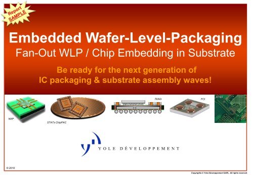
<strong>Embedded</strong> Wafer-Level-Packaging<br />
Fan-Out WLP / Chip Embedding in Substrate<br />
Be ready for the next generation of<br />
IC packaging & substrate assembly waves!<br />
Infineon<br />
Nokia<br />
FCI<br />
AT&S<br />
NXP<br />
STATs ChipPAC<br />
© 2010<br />
Copyrights © Yole Développement SARL. All rights reserved.
Table of Contents (1/2)<br />
• Scope of the Report & Definitions …...……. 3<br />
– Objectives of the report ………….……... 4<br />
• Executive Summary ………………………..… 9<br />
1) <strong>Embedded</strong> Packaging of active dies and<br />
passive components ………………….……. 10<br />
– Motivations and Drivers ………………... 18<br />
– Applications & End-markets: Status of<br />
commercialization …………………..…... 24<br />
• Cell-phone & Consumer applications<br />
• Automotive applications<br />
• Medical applications<br />
– 2009-2015 market forecasts for <strong>Embedded</strong><br />
packages ………………………………….... 32<br />
• In Package shipments (Munits)<br />
• In Packaging revenues ($M)<br />
– Supply chain emerging for embedded dies<br />
………………………………….…………….. 44<br />
• Players and positioning in the electronic value<br />
chain<br />
• Who is the most aggressive in the<br />
commercialization?<br />
• Who is doing what: partnership identified<br />
– Technology flavors for embedded package ... 51<br />
• Chip first versus chip last?<br />
• Single die embedding versus SiP module?<br />
• SiP multi-die integration<br />
• Discrete passive integration<br />
• Specific features integration (silicon interposers,<br />
holes, fluidic, hermetic cavities, etc…)<br />
• Challenges related to yield & supply chain<br />
– Equt & Material Tool-Box for <strong>Embedded</strong> die … 78<br />
– Cost structure for <strong>Embedded</strong> package<br />
manufacturing …………………………………..... 95<br />
• Comparison with competitive package alternative<br />
that <strong>Embedded</strong> die technology is looking for direct<br />
replacement (QFN, BGA, WLCSP, SOT, PoP…)<br />
• Cost structure target of <strong>Embedded</strong> die for different<br />
application case (RFID, IPD, Power MOSFET / IGBT,<br />
DC/DC converters, PMU, Wireless Connectivity ICs,<br />
Digital Baseband, Memories, etc …)<br />
– Conclusion on “sweets spots” for the<br />
introduction of <strong>Embedded</strong> die technology in the<br />
short / medium / long term ……………………. 102<br />
• Global Roadmap for <strong>Embedded</strong> die<br />
© 2010 • 2<br />
Copyrights © Yole Développement SARL. All rights reserved.
Table of Contents (2/2)<br />
2) Fan-Out WLP technology development … 120<br />
– Motivations and market drivers ………….... 44<br />
• Thermal performance of FOWLP package<br />
compared to FC-BGA package solution<br />
– Applications & status of commercialization<br />
– 2009-2015 market forecasts for FOWLP type of<br />
packages …………………………………….... 32<br />
• In Package shipments (Munits)<br />
• In Packaging revenues ($M)<br />
– Supply chain emerging for FOWLP ……….. 44<br />
• Players and positioning in the electronic value<br />
chain<br />
• Who is the most aggressive in the<br />
commercialization?<br />
• Who is doing what: partnership identified<br />
– FOWLP technologies and challenges<br />
• Who owns the IP in this space?<br />
• 1 st generation versus 2 nd generation FOWLP<br />
– TMV “Through Mold Via” fabrication<br />
• “Panel size” future manufacturing for FOWLP<br />
• Passive integration with FO-WLP technologies<br />
– Equipment & Materials for FO-WLP<br />
• Challenges in new material‟s selection and<br />
missing equipments<br />
– Cost structure for FO-WLP manufacturing<br />
• Competitive package alternative that FOWLP<br />
technology is looking for direct replacement<br />
(FC-CSP, FC-BGA, WB-BGA, PoP, etc…)<br />
• Cost structure for FOWLP by application (RF<br />
connectivity, Transceiver, PMU, wireless<br />
baseband SOC chip, etc…)<br />
– Conclusion on “sweets spots” for<br />
introduction of FOWLP technology in short<br />
/ medium / long term<br />
– Global Roadmap for Fan-Out WLP<br />
• Conclusion & Perspectives ….……… 136<br />
– Application space for each generation of<br />
FO-WLP & <strong>Embedded</strong> die technology<br />
– Impact of 3D TSV and silicon interposer<br />
technology concepts<br />
– Global 3D Packaging development<br />
roadmaps mixing interposer, FOWLP and<br />
<strong>Embedded</strong> die technologies<br />
• Appendix ……....…………….…….…… 152<br />
– Yole Developpement company<br />
presentation & services ..................... 183<br />
© 2010 • 3<br />
Copyrights © Yole Développement SARL. All rights reserved.
Scope of the Report<br />
Wafer-Scale-Packaging Platforms<br />
Wafer-Level<br />
Electrical Redistribution<br />
Wafer-Level<br />
Interface / Encapsulation<br />
Flip-chip & Wafer-Level<br />
Stacking / Integration<br />
WL-CSP<br />
‘Fan-in’<br />
FO-WLP<br />
‘Fan-Out’<br />
MEMS &<br />
Sensors<br />
Capping<br />
LED &<br />
Sensors<br />
Optics<br />
Systems<br />
with<br />
Fluidic<br />
<strong>Embedded</strong> IC<br />
in PCB / laminate<br />
3D IC<br />
& TSV<br />
Si on Si<br />
flip-chip<br />
Flip-chip<br />
BGA<br />
Courtesy of DALSA<br />
FOCUS of this<br />
new research report!<br />
FOCUS of this<br />
new research report!<br />
© 2010 • 4<br />
Copyrights © Yole Développement SARL. All rights reserved.
Objectives of the Report<br />
• This is the first report on <strong>Embedded</strong> Wafer-Level-Packaging technologies<br />
and markets from Yole Developpement.<br />
• The objectives of this first report are the followings:<br />
– Both Fan-Out WLP and Chip embedded package technologies analyzed<br />
– Key market drivers, benefits and challenges application by application<br />
– Market trends & figures with detailed breakdown by application<br />
– Description of the complete manufacturing BOM for embedded wafer level<br />
packaging:<br />
o Key equipments: for 200mm / 300mm / Panel manufacturing<br />
o Specific material‟s selection coming from both FE / BE / PCB / LCD area<br />
– Analysis of several embedded package target prices for a few key applications<br />
– Supply chain perspectives, key players and emerging infrastructure for<br />
embedded packaging<br />
o Analysis of the different possibility for the implementation of FO-WLP and chip<br />
embedding with the rationale behind (chip first / chip last, single die / multi-die / SiP<br />
module, etc …)<br />
© 2010 • 5<br />
Copyrights © Yole Développement SARL. All rights reserved.
Who should be interested in this Report?<br />
• Integrated semiconductor Device<br />
Manufacturers and fabless IC companies<br />
– Benchmark the industrialization status of<br />
embedded packaging technologies within the<br />
industry<br />
– Identify possible partnership /or second<br />
source packaging subcontractors for your<br />
forthcoming developments<br />
• Assembly and Test Service companies<br />
– Get the list of the main companies interested<br />
in <strong>Embedded</strong> WLP<br />
– Screen possible new applications and<br />
technologies to support diversification<br />
strategy with embedded packaging platform<br />
• Electronic module makers and Original<br />
Equipment Makers<br />
– Evaluate the availability and benefits of using<br />
embedded package components in your end<br />
system<br />
– Monitor different embedded WLP suppliers<br />
to adjust your sourcing strategy<br />
• PCB and IC substrate manufacturers<br />
– Monitor the evolution of IC packaging,<br />
assembly and test, especially linked to the<br />
emerging chip embedding<br />
– PCB-based technologies, FO-WLP, IPD and<br />
3D interposers<br />
• Equipment and Material suppliers<br />
– Understand the differentiated value of your<br />
products and technologies in this emergin<br />
but fast growing market<br />
– Identify new business opportunities and<br />
prospects<br />
© 2010 • 6<br />
Copyrights © Yole Développement SARL. All rights reserved.
Companies cited in this Report<br />
3D-Plus, ACET, ADTEC Engineering, Amkor, ams, Analog Devices,<br />
AT&S, Aptos, Asahi Glass, ASE, ASM, Atotech, Broadcom, Bosch,<br />
Camtek, Casio Micronics, CIRETEC, CMK, Compass Technology,<br />
CSR, Datacon, Daeduck, Denso, Dialog Semiconductor, Dow<br />
Corning, DuPont Electronics, Dyconex, Epic, EVGroup, Fico Molding,<br />
Flip-chip International, Fraunhofer-IZM, Freescale, Fujitsu, HD<br />
Microsystems, Hynix Semiconductor, Ibiden, Imbera, IME, IMEC,<br />
Infineon, ipdia, ITRI, KYEC, Leti, Lintec, LG Electronic, Micron,<br />
MicroChem, Mitsui, Murata, Nagase ChemteX, NANIUM, NEC<br />
Electronics, Nitto Denko, Nokia, NSC, NXP, Oki Electric, ORC,<br />
Panasonic, PPT, Qualcomm, Renesas, Rohm & Hass, Rudolph<br />
technologies, Samsung, SEMCO, Shinko Electric, SPIL, STATS<br />
ChipPAC, ST-Ericsson, STMicroelectronics, SPTS, SMIC, Shin-Etsu,<br />
SÜSS Microtec, Taiyo Yuden, TDK, Tessera, Texas Instruments, tok,<br />
Tong Hsing, Toray chemical, Toray Engineering, Toshiba, Towa,<br />
Triquint, UMTC, Unimicron, Unovis, UTAC, Vertical Circuits, Wolfson<br />
Microelectronics, Yamada and more…<br />
© 2010 • 7<br />
Copyrights © Yole Développement SARL. All rights reserved.
Market Trends<br />
• Historically, embedded wafer-level-packaging<br />
technology is not new at all<br />
– Several players such as Freescale with its RCP, Infineon with its<br />
eWLB and Ibiden for die embeddeding into PCB laminated<br />
substrates have developed dedicated technologies and process IP<br />
in this area for years.<br />
– Benefits of embedded package integration include miniaturization,<br />
improvement of electrical and thermal performance, cost<br />
reduction and simplification of logistic for OEMs<br />
1st generation eWLB cross-section<br />
(Courtesy of Infineon)<br />
Multi-chip SiP Module<br />
based on Chip Embedding technology<br />
(Courtesy of AT&S)<br />
<strong>Embedded</strong> die iBGA package<br />
(Courtesy of Imbera / Daeduck)<br />
Integrated passive IC “ready” for<br />
embedding into PCB laminate<br />
(Courtesy of NXP / FCI)<br />
• Things are moving<br />
really fast at the<br />
moment<br />
– This year, we see both<br />
Fan-Out wafer level<br />
packaging and chip<br />
embeddeding into PCB<br />
laminate package<br />
infrastructures emerging<br />
at the same time,<br />
ramping to high volume<br />
production<br />
© 2010 • 8<br />
Copyrights © Yole Développement SARL. All rights reserved.
Fan-out WLP Concept<br />
• A new SiP-friendly package platform processed at the wafer / panel level<br />
with built-in substrate routing.<br />
© 2010 • 9<br />
Copyrights © Yole Développement SARL. All rights reserved.
WL-CSP Applications Space<br />
Logic Basebands<br />
RF connectivity<br />
Multi-Mode<br />
Transceivers<br />
PMUs<br />
CMOS image sensors<br />
Wireless RF chips:<br />
- GPS + Bluetooth<br />
- FM radio<br />
<strong>Embedded</strong> WLP<br />
technologies are<br />
extending WLCSP<br />
application space to<br />
higher pin counts:<br />
> 140-300 I/Os<br />
IPD for ESD/EMI<br />
LED Drivers<br />
MEMS inertials<br />
(gyroscopes, accelerometers)<br />
Logic / analog parts<br />
Audio Amplifiers<br />
Operational Amplifiers<br />
MEMS (RF, Siliconmicrophones…)<br />
Headphones drivers<br />
Temperature sensors<br />
MOSFET<br />
5 10 > 50 >100<br />
200-350<br />
I/Os<br />
© 2010 • 10<br />
Copyrights © Yole Développement SARL. All rights reserved.
Fan-Out WLP technology is emerging<br />
on both 200mm / 300mm infrastructures<br />
• Infineon is having a great sucess with its proprietary eWLB technology<br />
– The first FO-WLP eWLB wafers are mass produced on 200mm both Infineon (GE), ASE (TW) and<br />
StatschippaC (SG) since 2009.<br />
– Indeed, Fan-Out WLP is extending the general concept of Wafer Scale Packaging to new application<br />
categories, especially the ones with higher pin-counts and larger chip size such as wireless<br />
communication ICs<br />
• First embedded wafer-level-package products based on eWLB have been<br />
identified within LGE and Nokia handsets<br />
– This year, a few additional players<br />
are even more aggressive in<br />
putting further capacity for eWLB<br />
manufacturing as both<br />
StatschippaC (SG) and NANIUM<br />
(PT) are at the moment rampingup<br />
their facilities for<br />
manufacturing the first generation<br />
eWLB of Infineon on 300mm<br />
reconfigured wafers<br />
– Other packaging houses such as<br />
SPIL, Amkor, UTAC and others<br />
are also on the point to announce<br />
the start of their own Fan-out<br />
wafer level packaging operations<br />
300mm eWLB reconfigured wafer<br />
(Courtesy of NANIUM)<br />
© 2010 • 11<br />
Copyrights © Yole Développement SARL. All rights reserved.
<strong>Embedded</strong> die package technology<br />
to expand fast from niche to high volume markets<br />
• At the same time, embedded die package technology has made a lot of progress on its side !<br />
– Based on PCB laminate infrastructure, chip embeddeding technology is actually on the way to catch a<br />
relatively important portion of the actual „Fan-in‟ WLCSP packaging business as it does leverage the<br />
existing WLP/RDL infrastructure already established worldwide: indeed, most of WLCSP die applications are<br />
“embedded ready”, so to realize the full benefits of this “WLCSP to <strong>Embedded</strong> die” conversion, only a few<br />
extra manufacturing steps are missing like the realization of thin copper plating process, extreme wafer<br />
thinning down to 50μm, thin dies handling and dicing.<br />
© 2010 • 12<br />
iBGA embedded die wafer-level-package cross-section (Courtesy of Imbera / Daeduck)<br />
• Electrical performance, testing and manufacturing yields are still major issues and<br />
showstoppers for chip embedding technology to move forward<br />
– Therefore, initial volume markets for embedded packages will be rather small, low pin-counts analog type of<br />
applications such as integrated passive devices (IPD), RFID and power MOSFET components that are at the<br />
moment under qualification for mass production before the end of this year already.<br />
– Generally speaking, we believe that the winning situation for embedded die packages can be met for<br />
company partnerships able to cross-over the traditional packaging, assembly and test supply chain. A good<br />
example would be to put together a leading analog IC player (such as TI, Maxim IC, NXP or ST) with a<br />
WLP/RDL partner (such as FCI, Casio Micronics, NEPES, etc…) together with a PCB integrator player (such<br />
as Imbera / Daeduck, Ibiden, AT&S, Taiyo Yuden or SEMCO). This type of emerging partnerships are<br />
absolutely necessary in order to standardize the embedded package technology and to leverage an entire<br />
new packaging infrastructure based on low-cost, panel size PCB manufacturing techniques.<br />
Copyrights © Yole Développement SARL. All rights reserved.
FOWLP versus Chip Embedding:<br />
Competing technologies and infrastructures ?<br />
• Today, embedded die and Fan-Out WLP technologies are not competing<br />
– Indeed, these two emerging semiconductor packaging techniques are targeting very different<br />
applications initially: the chip embeddeding technology is looking for replacement of low cost, low<br />
pin-counts WLCSP / SOT / QFN / LGA family package applications while FOWLP technology is rather<br />
targeting the direct replacement of higher I/Os (> 120 pins) BGA package applications.<br />
• What about tomorrow?<br />
– However, in the long term, with<br />
standardization and through further<br />
technology improvements towards<br />
higher yield, better electrical<br />
performance, lower profile, better<br />
testability and smaller pitch features,<br />
Fan-out WLP and <strong>Embedded</strong> die<br />
technology could seriously compete in<br />
the fast growing 3D Packaging market<br />
space as they will both enable the<br />
construction of ever more complex,<br />
larger SiP modules with different active<br />
and passive functions, all connected on<br />
both sides of the active substrate…<br />
Overall tool-box solutions for 3D Packaging<br />
(Source Yole Developpement)<br />
• So Fan-out WLP and chip embeddeding into PCB laminates are just two additional<br />
key pieces of the widening tool-box for 3D Packaging!<br />
© 2010 • 13<br />
Copyrights © Yole Développement SARL. All rights reserved.
Current / Future Tool-Box for 3D Packaging<br />
I/O<br />
. Count<br />
> 1 000<br />
TSV<br />
Silicon/Glass<br />
WLP <strong>Embedded</strong> BGA/PoP<br />
Logic<br />
3-D SOC<br />
Silicon PoP<br />
3-D Logic SiP<br />
3-D Flip-Chip<br />
500<br />
300<br />
120<br />
50<br />
15<br />
MEMS<br />
WLP<br />
3-D<br />
RF-SiP<br />
WLP Fan-Out<br />
Logic<br />
eFlash<br />
eDRAM<br />
Analog<br />
RF + I/Os<br />
Interposer<br />
WLP Fan-in<br />
FO WLP - SiP<br />
<strong>Embedded</strong> <strong>Die</strong><br />
<strong>Embedded</strong> PoP<br />
FO WLP - MCP<br />
<strong>Embedded</strong> SiP Module<br />
PoP ‟Bottom Package‟ evolution:<br />
Face to Face<br />
TMV<br />
PoP High Density<br />
2<br />
© 2010 • 14<br />
2mm2<br />
20mm2 50mm2 80mm2 100mm2 500mm2<br />
Copyrights © Yole Développement SARL. All rights reserved.<br />
Chip /<br />
Package<br />
Size
<strong>Embedded</strong> Wafer-Level-Package technologies<br />
Fan-out WLP<br />
• Wafers or panels are<br />
(re)configured<br />
FO-WLP<br />
– By placing known good ICs active<br />
face down on a foil and by overmolding<br />
them<br />
– These wafers/panels are then<br />
flipped and processed back in the<br />
wafer fab with RDL, bumping, …<br />
<strong>Embedded</strong><br />
IC in PCB<br />
Chip embedding<br />
(or embedded IC in PCB)<br />
• Known good ICs and picked<br />
– and placed on top of an organic<br />
layer of Printed circuit board<br />
– Subsequent layers are laminated<br />
on top and regular PCB<br />
manufacturing operations take<br />
place on the panel with the<br />
embedded ICs<br />
© 2010 • 15<br />
Both these technologies are considered (n+1) technologies versus<br />
WLCSP. Among others, they offer the following differential benefits:<br />
fan-out area for larger IO densities than WLCSP<br />
Collective wafer level processing of known good dice (KGD)<br />
Higher expected second level reliability (package connection to the<br />
mother board)<br />
Back-side protection<br />
System-in-package and 3D integration capabilities<br />
Copyrights © Yole Développement SARL. All rights reserved.
Some more slides extracted from the Report …<br />
© 2010 • 16<br />
Copyrights © Yole Développement SARL. All rights reserved.
About the Authors of this Report<br />
• Jean-Marc Yannou<br />
– Jean-Marc recently joined Yole Développement as technology and<br />
market expert in the fields of advanced packaging and Integrated<br />
Passive Devices. He has 15-years of experience in the<br />
semiconductor industry. He worked for Texas Instruments and<br />
Philips (then NXP semiconductors) where he served as<br />
“Innovation Manager” for System-in-Package technologies<br />
Contact: yannou@yole.fr<br />
• Jerome Baron<br />
– Jerome is leading the MEMS & Advanced Packaging market<br />
research at Yole Developpement. He is leading the MEMS and<br />
Advanced Packaging market research at Yole. He has been<br />
involved in the technology analysis of the 3D packaging market<br />
evolution at device, equipment and material supplier levels. He<br />
was granted a Master of Science degree in Nanotechnologies from<br />
the National Institute of Applied Sciences in Lyon, France<br />
Contact: baron@yole.fr<br />
© 2010 • 17<br />
Copyrights © Yole Développement SARL. All rights reserved.
How to stay connected in the<br />
Advanced Packaging area with us?<br />
Market Research Reports &<br />
Strategy Consulting Services<br />
Publications & Newsletters<br />
Wafer Level Packaging<br />
2009 Report<br />
www.yole.fr<br />
www.i-micronews.com/3DIC.asp<br />
© 2010 • 18<br />
Copyrights © Yole Développement SARL. All rights reserved.
What about on-site workshops?<br />
• Off-the-shelf Reports will never meet all your expectations because<br />
they are inherently built to cover a wide range of applications,<br />
markets, technologies and players<br />
• Our analysts also have the possibility to prepare presentations and<br />
on-site workshops at your company place for:<br />
– De-briefing your team on several specific topics described within the report<br />
– Prepare a face to face Q&A session: your company‟s experts send a list of<br />
questions in advance. Based on this list, our analysts can elaborate a „more<br />
focused‟ analysis and presentation on what really matters for you!<br />
For more information about the possible<br />
organization of workshops with Yole‟s<br />
analysts, please contact us.<br />
© 2010 • 19<br />
Copyrights © Yole Développement SARL. All rights reserved.


