

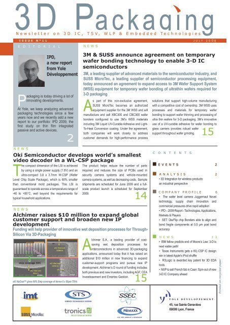
3M & SUSS announce agreement on temporary wafer ... - I-Micronews
3M & SUSS announce agreement on temporary wafer ... - I-Micronews
3M & SUSS announce agreement on temporary wafer ... - I-Micronews

Create successful ePaper yourself
Turn your PDF publications into a flip-book with our unique Google optimized e-Paper software.
N e w s l e t t e r o n 3 D I C , T S V , W L P & E m b e d d e d T e c h n o l o g i e s<br />
I S S U E N ° 1 1 J U L Y 2 0 0 9<br />
E D I T O R I A L N E W S<br />
IPD,<br />
a new report<br />
from Yole<br />
Développement<br />
Packaging is today driving a lot of<br />
innovating developments.<br />
At Yole, we keep analyzing advanced<br />
packaging technologies since a few<br />
years now and we recently add a new<br />
report to our portfolio: IPD 2009, the<br />
first study <strong>on</strong> thin film integrated<br />
passive and active devices.<br />
2<br />
<str<strong>on</strong>g>3M</str<strong>on</strong>g> & <str<strong>on</strong>g>SUSS</str<strong>on</strong>g> <str<strong>on</strong>g>announce</str<strong>on</strong>g> <str<strong>on</strong>g>agreement</str<strong>on</strong>g> <strong>on</strong> <strong>temporary</strong><br />
<strong>wafer</strong> b<strong>on</strong>ding technology to enable 3-D IC<br />
semic<strong>on</strong>ductors<br />
<str<strong>on</strong>g>3M</str<strong>on</strong>g>, a leading supplier of advanced materials to the semic<strong>on</strong>ductor industry, and<br />
<str<strong>on</strong>g>SUSS</str<strong>on</strong>g> MicroTec, a leading supplier of semic<strong>on</strong>ductor processing equipment,<br />
today <str<strong>on</strong>g>announce</str<strong>on</strong>g>d an <str<strong>on</strong>g>agreement</str<strong>on</strong>g> to expand access to <str<strong>on</strong>g>3M</str<strong>on</strong>g> Wafer Support System<br />
(WSS) equipment for <strong>temporary</strong> <strong>wafer</strong> b<strong>on</strong>ding of ultrathin <strong>wafer</strong>s required for<br />
3-D packaging<br />
As part of this n<strong>on</strong>-exclusive <str<strong>on</strong>g>agreement</str<strong>on</strong>g>,<br />
<str<strong>on</strong>g>SUSS</str<strong>on</strong>g> MicroTec becomes an authorized<br />
equipment supplier for the <str<strong>on</strong>g>3M</str<strong>on</strong>g> WSS and will<br />
manufacture and sell XBC300 and CBC300 <strong>wafer</strong><br />
b<strong>on</strong>ders c<strong>on</strong>figured to use <str<strong>on</strong>g>3M</str<strong>on</strong>g>’s WSS materials<br />
including <str<strong>on</strong>g>3M</str<strong>on</strong>g> Liquid UV-Curable Adhesive and Light-<br />
To-Heat C<strong>on</strong>versi<strong>on</strong> coating. Under the <str<strong>on</strong>g>agreement</str<strong>on</strong>g>,<br />
both companies will work closely to address<br />
customer demands for high-performance process<br />
soluti<strong>on</strong>s that support high-volume manufacturing<br />
with a competitive cost of ownership. <str<strong>on</strong>g>3M</str<strong>on</strong>g> WSS uses<br />
processes and materials for <strong>temporary</strong> <strong>wafer</strong><br />
b<strong>on</strong>ding to support <strong>wafer</strong> thinning and processing of<br />
ultra thin <strong>wafer</strong>s for 3-D packaging. <str<strong>on</strong>g>3M</str<strong>on</strong>g>’s innovative<br />
use of a UV-curable adhesive for <strong>wafer</strong> b<strong>on</strong>ding to<br />
glass carriers provides robust <strong>wafer</strong><br />
support throughout <strong>wafer</strong> grinding.<br />
15<br />
N E W S<br />
Oki Semic<strong>on</strong>ductor develops world’s smallest<br />
video decoder in a WL-CSP package<br />
The compact dimensi<strong>on</strong> of the LSI is achieved<br />
by using a single power supply (1.8V) and an<br />
ultra-compact 3.8 x 3.7mm W-CSP (Wafer<br />
Level Chip Scale Package), which is 60% smaller<br />
than c<strong>on</strong>venti<strong>on</strong>al mold packages. This LSI is<br />
guaranteed to operate across a temperature range of<br />
-40 to +85°C, well bey<strong>on</strong>d the requirements for<br />
typical household applicati<strong>on</strong>s.<br />
The product helps reduce the number of parts<br />
required and reduces the size of PCBs used in<br />
security camera systems and vehicle-mounted<br />
camera systems, as well as decreasing costs. Sample<br />
shipments are scheduled for June 2009 and a fullscale<br />
product launch is scheduled for September<br />
2009.<br />
14<br />
N E W S<br />
Alchimer raises $10 milli<strong>on</strong> to expand global<br />
customer support and broaden new IP<br />
development<br />
Funding will help provider of innovative wet depositi<strong>on</strong> processes for Through-<br />
Silic<strong>on</strong> Via 3D-Packaging<br />
eG ViaCoat gives 90% Step coverage of dense 5 x 50µm TSVs<br />
Alchimer S.A., a leading provider of costsaving<br />
wet depositi<strong>on</strong> processes for<br />
interc<strong>on</strong>necti<strong>on</strong>s in advanced 3D-packaging<br />
applicati<strong>on</strong>s, <str<strong>on</strong>g>announce</str<strong>on</strong>g>d today that it has raised an<br />
additi<strong>on</strong>al $10 milli<strong>on</strong> in new financing to expand<br />
customer-support programs and pursue new IP<br />
development. Alchimer’s D round of funding includes<br />
both previous and new investors, including AGF, CEA<br />
Investissement and Emertec Gesti<strong>on</strong>.<br />
15<br />
C O N T E N T S<br />
E V E N T S 2<br />
A N A L Y S I S 2<br />
• 3D Integrati<strong>on</strong> for wireless products:<br />
an industrial perspective<br />
C O M P A N Y P R O F I L E 6<br />
• The <strong>wafer</strong> level camera Juggernaut Novel<br />
technology, supply chain innovati<strong>on</strong> and<br />
commercial pressures drive rapid adopti<strong>on</strong><br />
• IPD – 2009 Report - Technologies, Applicati<strong>on</strong>s,<br />
Markets & Players<br />
• SET: Die/Flip chip B<strong>on</strong>ders able to align and<br />
b<strong>on</strong>d fragile comp<strong>on</strong>ents at 0.5 μm post b<strong>on</strong>d<br />
accuracy<br />
N E W S 1 3<br />
• IBM fellow predicts end of Moore’s Law: 3-D is<br />
next viable path!<br />
• Texas Instruments gets a WL-CSP IC design<br />
win in latest Apple’s iPod shuffle<br />
• R3Logic is awarded key patent for 3D EDA<br />
tools<br />
• NXP to sell French fab in Caen: Spin-out of new<br />
3-D IC Company ahead<br />
Printed <strong>on</strong> recycled paper<br />
45, rue Sainte Geneviève<br />
69006 Ly<strong>on</strong>, France
J U L Y 2 0 0 9 i s s u e n ° 1 1<br />
N e w s l e t t e r o n 3 D I C , T S V , W L P & E m b e d d e d T e c h n o l o g i e s<br />
Printed <strong>on</strong> recycled paper<br />
E D I T O R I A L<br />
As you will discover in the article<br />
in this last issue of 3D<br />
Packaging newsletter,<br />
Integrated Passive Devices (IPD’s)<br />
are growing industry trend.<br />
They can be used as <strong>wafer</strong>-level<br />
packaged single chip soluti<strong>on</strong>s for<br />
interface c<strong>on</strong>diti<strong>on</strong>ing, or they can be<br />
assembled with active IC’s in<br />
Systems-in-a-Package, or they can<br />
be used as package substrates or as<br />
system sub mounts.<br />
IPDs are also a nice example of a mix<br />
of technologies as both IC and MEMS<br />
worlds meet here, to offer higher<br />
performance with high integrati<strong>on</strong>.<br />
Our report is the first covering technology<br />
review for thin film IPD, descripti<strong>on</strong><br />
of the applicati<strong>on</strong>s, market forecasts,<br />
roadmaps & manufacturing<br />
challenges, descripti<strong>on</strong> of the supply<br />
chain with players profiles.<br />
Enjoy reading our newsletter!<br />
Dr Eric MOUNIER<br />
Editor in chief<br />
mounier@yole.fr<br />
E V E N T S<br />
• Semic<strong>on</strong> West,<br />
July 14-17, San Francisco, CA, USA<br />
• Semic<strong>on</strong> Europa,<br />
October 6-8, Dresden, Germany<br />
• 3-D Architectures for<br />
Semic<strong>on</strong>ductor Integrati<strong>on</strong> and<br />
Packaging, This is SEMICON Europa.<br />
December 9 – 11, 2009, San Francisco, CA,<br />
USA<br />
A N A L Y S I S<br />
3D Integrati<strong>on</strong> for wireless products: an<br />
industrial perspective<br />
The mobile ph<strong>on</strong>e and wireless industries have been growing at a very fast pace<br />
in the last 10 years. With more than 1.2 billi<strong>on</strong> ph<strong>on</strong>es sold in 2008, the wireless<br />
market has been <strong>on</strong>e of the main c<strong>on</strong>tributors in driving the development of the<br />
most advanced semic<strong>on</strong>ductor technologies. The computing power for portable<br />
devices is becoming mandatory to enable mobile internet browsing, mobile<br />
TV, and all increasing multimedia features. In that c<strong>on</strong>text, miniaturizati<strong>on</strong> and<br />
performance are the driving forces for silic<strong>on</strong> technology development.<br />
Following the ITRS roadmap with CMOS<br />
downscaling is the traditi<strong>on</strong>al way to proceed.<br />
But the R&D expenses to sustain such a<br />
roadmap are extremely selective. Only a few<br />
companies or c<strong>on</strong>sortia can afford it. That’s why<br />
advanced CMOS technology could start to be seen<br />
as a kind of commodity and integrati<strong>on</strong> with new<br />
soluti<strong>on</strong>s appears as a much str<strong>on</strong>ger differentiator<br />
element. Packaging c<strong>on</strong>tributi<strong>on</strong>s in the final product<br />
gained in importance. Major improvements and<br />
progresses have been d<strong>on</strong>e lately and a new<br />
soluti<strong>on</strong> is gaining more and more importance: 3D<br />
Integrati<strong>on</strong>.<br />
3D Packaging<br />
Despite the recent buzz in the industry for a couple<br />
of m<strong>on</strong>ths, 3D c<strong>on</strong>figurati<strong>on</strong>s are not new at all. In<br />
effect, 3D c<strong>on</strong>figurati<strong>on</strong>s at the packaging level have<br />
been 6–8 around OctOber, for years. In 2009 many teardowns Dresden, of Germany<br />
handsets, lot of 3D packages can be found. A stack<br />
of dice c<strong>on</strong>nect with wire b<strong>on</strong>ds with is something europe’s very comm<strong>on</strong> technology<br />
for memories. Package over Package (PoP) Leaders and expand Your Opportunities<br />
Package in Package (PiP) is a c<strong>on</strong>figurati<strong>on</strong><br />
widespread in Infinite to combine Ways. the stack of memories <strong>on</strong> top<br />
of an applicati<strong>on</strong> processor or digital baseband. At<br />
SEMICON Europa is the <strong>on</strong>ly event in Europe focused <strong>on</strong><br />
the same time, 3D package soluti<strong>on</strong>s such as<br />
embedded c<strong>on</strong>necting die in people laminate and or rebuilt companies <strong>wafer</strong> with such the as technologies<br />
Fan-Out and innovati<strong>on</strong>s Wafer Level making Packaging advanced (FO-WLP) microelectr<strong>on</strong>ics are and<br />
emerging. FO-WLP goal is to c<strong>on</strong>struct a package as<br />
related technologies possible. From device design to final<br />
small as possible to enable all the BGA balls to fit <strong>on</strong><br />
it. The manufacturing, packaging is built no around other the event individual Europe known brings CIS. you better<br />
good face-to-face die and provides c<strong>on</strong>tact a way with to make customers the laminate and technology<br />
substrate vanish. FO-WLP improves signal integrity,<br />
partners than SEMICON Europa.<br />
shortens interc<strong>on</strong>nects, reduces line/space for<br />
rerouting, and as a c<strong>on</strong>sequence, allows a reducti<strong>on</strong><br />
in the package See footprint. You at Infine<strong>on</strong> SeMIcON and Freescale europa 2009<br />
developed reGISter their own NOW: FO-WLP WWW.SeMIcONeurOpa.OrG<br />
technology<br />
respectively called eWLB TM and RCP TM . Lately,<br />
STMicroelectr<strong>on</strong>ics partnered with Infine<strong>on</strong> and<br />
STATS Chip Pac to develop the 2nd generati<strong>on</strong> of<br />
eWLB TM , 3D-eWLB TM , and enable 2-sided and<br />
c<strong>on</strong>sequently, 3D c<strong>on</strong>figurati<strong>on</strong>s.<br />
3D at IC level using TSV<br />
All the c<strong>on</strong>figurati<strong>on</strong>s menti<strong>on</strong>ed above are 3D at the<br />
packaging level. N<strong>on</strong>e of them uses TSV, which<br />
could allow “real” 3D at the IC level in some<br />
c<strong>on</strong>figurati<strong>on</strong>s. TSVs are nothing more than a techno<br />
brick that allows dice to interc<strong>on</strong>nect <strong>on</strong> the vertical<br />
axis at the IC level. The impact of TSV is that these<br />
short interc<strong>on</strong>necti<strong>on</strong>s could enable a new split of<br />
functi<strong>on</strong>s and new product partiti<strong>on</strong>ing. However, it<br />
is important to notice that TSV interc<strong>on</strong>necti<strong>on</strong>s can<br />
be d<strong>on</strong>e at different levels and the impact <strong>on</strong> final<br />
applicati<strong>on</strong>s is not the same. Either the TSV is d<strong>on</strong>e<br />
at the b<strong>on</strong>d pad level or at the global interc<strong>on</strong>nect<br />
level.<br />
At the b<strong>on</strong>d pad level, TSV is d<strong>on</strong>e in a via last<br />
process in a <strong>wafer</strong> level packaging fab envir<strong>on</strong>ment.<br />
The pitch of TSV is in the range of a b<strong>on</strong>d pad pitch.<br />
Typical values from 50 to 150µ in term of pitch can<br />
be c<strong>on</strong>sidered. An aspect ratio can reach 5:1 and<br />
filling is c<strong>on</strong>formal or full. RLC electrical performances<br />
are better than wire b<strong>on</strong>ds, except for the capacitance<br />
that may remain high. This type of TSV can be based<br />
<strong>on</strong> an improvement of technologies developed for<br />
At the global interc<strong>on</strong>nect level, we c<strong>on</strong>sider TSV<br />
with higher aspect ratio d<strong>on</strong>e in foundry envir<strong>on</strong>ment,<br />
preferably via middle (after FEOL but before BEOL)<br />
or first (before FEOL). TSV pitch is in the 10-20µ<br />
range with the aspect ratio ranging from 5:1 to 10:1<br />
Fig1 - FOWLP 1 side (left) , 2 sides (called 3D-eWLB, right)<br />
2
J U L Y 2 0 0 9 i s s u e n ° 1 1<br />
N e w s l e t t e r o n 3 D I C , T S V , W L P & E m b e d d e d T e c h n o l o g i e s<br />
Fig2 - From design to packaging: dem<strong>on</strong>strati<strong>on</strong> achieved between STMicroelectr<strong>on</strong>ics and CEA-LETI<br />
or even a bit more. For this category of TSV, dice are<br />
not <strong>on</strong>ly c<strong>on</strong>nected at b<strong>on</strong>d pad level but also at the<br />
IP block or memory bank levels for instance. This<br />
type of TSV enables the achievement of structures<br />
with very short interc<strong>on</strong>necti<strong>on</strong>s and good electrical<br />
performances. True heterogeneous integrati<strong>on</strong> is<br />
made possible and SoC–like features can be<br />
realized but using the third dimensi<strong>on</strong> and not <strong>on</strong>ly<br />
the x-y directi<strong>on</strong>s. Dice interc<strong>on</strong>nected with this type<br />
of TSV are closer to SoC than SiP. For these<br />
reas<strong>on</strong>s, 3D SoC is a very good term for this<br />
c<strong>on</strong>figurati<strong>on</strong>. Figure 1 shows key dem<strong>on</strong>strati<strong>on</strong><br />
achieve in STMicroelectr<strong>on</strong>ics with CEA-LETI.<br />
Complementarity of 3D packaging and 3D IC<br />
Except for some <strong>wafer</strong>-level chip-scale packages<br />
(WLCSP) or silic<strong>on</strong> interposer with TSV directly<br />
mounted <strong>on</strong> Printed Wiring Board (PWB) with a BGA<br />
balls, TSV is not a packaging soluti<strong>on</strong> by itself. TSV<br />
uses <strong>on</strong>ly “back-end world” skills such as b<strong>on</strong>ding,<br />
fine pitch bumping, back grinding and thin <strong>wafer</strong><br />
handling, for instance. In effect, final packaging is<br />
required to c<strong>on</strong>nect the device to the PWB. And due to<br />
assembly c<strong>on</strong>straints, the choice of the final package<br />
soluti<strong>on</strong> could impact the entire TSV process flow.<br />
Fig3 - 3D IC TSV stack in 3D-eWLB (Courtesy of ST-Ericss<strong>on</strong>)<br />
This final packaging could be a BGA package, a Fan-<br />
Out WLP type, an embedded die in laminate, or other.<br />
Here, it is interesting to notice how complementary<br />
3D IC c<strong>on</strong>figurati<strong>on</strong>s with TSV and 3D packaging<br />
can be. In effect, 3D eWLB TM can enable designs to<br />
fully benefit from the 3D IC integrati<strong>on</strong>, and for<br />
instance, reduce the package footprint with more<br />
aggressive design rules than BGA packages. TSV is<br />
a new technology and 3D eWLB TM a new packaging<br />
technology as well. Only c<strong>on</strong>sidering BGA-type<br />
packages for structures with TSV might be a wr<strong>on</strong>g<br />
reas<strong>on</strong>ing. Some c<strong>on</strong>straints can even be relaxed<br />
by coupling 3D IC TSV with 3D advanced packaging<br />
and then the full benefits of the TSV can emerge.<br />
Issues such as thin <strong>wafer</strong> handling can, for instance,<br />
be simplified.<br />
3D Integrati<strong>on</strong>: C<strong>on</strong>vergence of<br />
Architecture with Silic<strong>on</strong> & Package and<br />
Out of the box thinking required.<br />
3D IC TSV is the c<strong>on</strong>vergence of silic<strong>on</strong> and<br />
packaging with the design. New architectures can in<br />
effect be c<strong>on</strong>sidered and achieved. In fact, new<br />
architectures have to be c<strong>on</strong>sidered if cost<br />
effectiveness is to be reached.<br />
In order to fully benefit from 3D TSV and make this<br />
technology cost effective, 3D architecture needs to<br />
be c<strong>on</strong>sidered at a very early stage. However,<br />
designers are facing a gap between TSV technology<br />
process and TSV system design. This gap is due to<br />
the fact that there is no clear TSV technology<br />
roadmap in the industry. With a scaling-based<br />
approach and a classical follow-up of Moore’s law, it<br />
was easier to focus the R&D efforts and predict the<br />
size and performance of a new techno node. With<br />
3D TSV, the industry is facing a new paradigm.<br />
Designers’ mentalities have to be modified and the<br />
former c<strong>on</strong>straints of 2D have to be partially<br />
forgotten.<br />
Roadmaps exist, but are not necessarily very<br />
relevant. For this reas<strong>on</strong>, many opti<strong>on</strong>s can be<br />
c<strong>on</strong>sidered, and process technologists do not know<br />
by themselves where to go and <strong>on</strong> what to focus.<br />
The <strong>on</strong>ly soluti<strong>on</strong> is to reinforce collaborati<strong>on</strong>s and<br />
discussi<strong>on</strong>s between the design community and the<br />
hardware technology community. A holistic approach<br />
is necessary to find the technology / design sweet<br />
spot and the applicati<strong>on</strong> needs to drive developments.<br />
Applicati<strong>on</strong> roadmap<br />
Applicati<strong>on</strong>s that could use TSV and 3D remain a hot<br />
questi<strong>on</strong>. Only a few people have clear views <strong>on</strong><br />
products that could use such innovati<strong>on</strong>s. Many<br />
niche markets would exist, for sure. However, when<br />
we think about core chipset comp<strong>on</strong>ents in wireless,<br />
the scope of applicati<strong>on</strong>s tends to reduce. The<br />
following roadmap is based <strong>on</strong> ST-Ericss<strong>on</strong>’s and<br />
STMicroelectr<strong>on</strong>ics’ view and portfolio for wireless<br />
products (fig 2). Memory stacks with TSV such as<br />
DRAM are not menti<strong>on</strong>ed as they are not part of the<br />
company business area anymore. Combinati<strong>on</strong>s of<br />
3D IC TSV with advanced packaging such as 3D<br />
eWLB TM are not detailed <strong>on</strong> the schematics.<br />
The first CMOS Imaging Sensors are now <strong>on</strong> the<br />
market and ramping up. The possibility to substitute<br />
Printed <strong>on</strong> recycled paper<br />
3
J U L Y 2 0 0 9 i s s u e n ° 1 1<br />
N e w s l e t t e r o n 3 D I C , T S V , W L P & E m b e d d e d T e c h n o l o g i e s<br />
beginning and much more will be discovered and<br />
understood in up-coming years. The <strong>on</strong>ly thing to<br />
avoid with 3D Integrati<strong>on</strong> is to c<strong>on</strong>tinue thinking<br />
based <strong>on</strong> the past experiences of downscaling.<br />
Applying Moore’s law based <strong>on</strong> scaling to a More<br />
than Moore approach such as 3D Integrati<strong>on</strong> TSV is<br />
not necessary at all. The applicati<strong>on</strong> should help in<br />
the roadmap definiti<strong>on</strong>.<br />
Printed <strong>on</strong> recycled paper<br />
Fig 4 - Applicati<strong>on</strong> Roadmap for 3D integrati<strong>on</strong> in wireless products (Courtesy of ST-Ericss<strong>on</strong>)<br />
wires by c<strong>on</strong>necti<strong>on</strong>s coming from the backside of<br />
the die would gain them a reducti<strong>on</strong> in the camera<br />
volume and its cost. However, in this example, we<br />
can’t speak about TSV enabling 3D c<strong>on</strong>figurati<strong>on</strong><br />
because, in fact, no chips are c<strong>on</strong>nected al<strong>on</strong>g the<br />
vertical axis. The top layer is <strong>on</strong>ly a glass carrier, not<br />
an active die; this can be called 2.5D but definitively<br />
not 3D.<br />
Power Amplifiers (PA) built in SOI are likely to use<br />
TSV technology in the future in order to improve<br />
performance and reduce die size. For PA, TSV is<br />
<strong>on</strong>ly used for parasitic and each is c<strong>on</strong>nected to a<br />
comm<strong>on</strong> ground <strong>on</strong> the metallized backside of the<br />
chip. Wires remain for I/O. In that case, a very low<br />
cost TSV technology is compulsory. Thermal<br />
dissipati<strong>on</strong> improvement is foreseen as well.<br />
The first true 3D ICs using TSV are forecasted for<br />
2012. New partiti<strong>on</strong>ing of chips with IP in the best<br />
techno node will appear. Logic dice would be from<br />
different techno node generati<strong>on</strong>s (N generati<strong>on</strong>,<br />
N+1, N+2…). A smart split of functi<strong>on</strong>s will be d<strong>on</strong>e<br />
in order to achieve the right cost/performance tradeoff<br />
with TSV as the new enabler. An intermediate<br />
step based <strong>on</strong> a silic<strong>on</strong> interposer for the bottom die,<br />
c<strong>on</strong>taining <strong>on</strong>ly routing and few functi<strong>on</strong>s, is likely to<br />
happen. It will help in bridging the gap toward 3D<br />
SoC and a full readiness of design tools. With 3D IC<br />
and TSV, new topics will need to be c<strong>on</strong>sidered.<br />
Numbers of opti<strong>on</strong>s in silic<strong>on</strong> <strong>wafer</strong>s, such as the<br />
type of ESD protecti<strong>on</strong> and test strategy are a few. A<br />
key advantage of 3D IC for this scheme of integrati<strong>on</strong><br />
is clearly the time reducti<strong>on</strong> of critical IP development<br />
in an advanced techno node. With a smart<br />
partiti<strong>on</strong>ing, complexity will be reduced and no<br />
l<strong>on</strong>ger <strong>on</strong> the critical path.<br />
A memory / logic stack using TSV is a type of<br />
applicati<strong>on</strong> the industry often refers to. The main<br />
reas<strong>on</strong> for this is the increased bandwidth required<br />
by the final applicati<strong>on</strong>s (driven by video features<br />
such as 1080p30 playback, 1080p30, 60, 120<br />
Camcorder, 3D gaming…). With a new memory /<br />
logic interface architecture, based for instance <strong>on</strong> a<br />
wide I/O approach, this bandwidth challenge might<br />
be overcome. Furthermore, this new wide I/O<br />
interface with parallel access to the memory will<br />
enable lower power c<strong>on</strong>sumpti<strong>on</strong> in the memory bus.<br />
For cellular ph<strong>on</strong>es, this bandwidth bottleneck might<br />
come after the Low Power DDR2 memory<br />
generati<strong>on</strong>. However, many challenges are rising.<br />
Thermal management is definitively a critical point in<br />
this approach. In effect, the power dissipati<strong>on</strong> of the<br />
logic die, typically an applicati<strong>on</strong> processor or a<br />
digital baseband, can heat the memory directly<br />
stacked <strong>on</strong> top. As memories have a lower Tj than<br />
logic die (85°C or 105°C), the memory will receive<br />
too much heat and w<strong>on</strong>’t work correctly. Power<br />
dissipati<strong>on</strong> of the bottom die will be range from 1 to 3<br />
W from low to high end 3G platforms.<br />
Another main issue with the wide I/O memory is the<br />
standardizati<strong>on</strong> and supply chain. Most of the time,<br />
the memory and logic die will come from different<br />
companies. Standardizati<strong>on</strong> will be required to<br />
enable the final OEM integrator to source different<br />
memory types or any double sourcing.<br />
C<strong>on</strong>clusi<strong>on</strong>s<br />
Roadmaps will mature during the next few years as<br />
people begin to understand all the capabilities of 3D<br />
Integrati<strong>on</strong>. As of today, <strong>on</strong>ly the emerging part of the<br />
iceberg is visible. 3D thinking is <strong>on</strong>ly at its early<br />
It is crucial to differentiate 3D packaging and 3D at<br />
the IC level using TSV. TSV by itself is not a<br />
packaging technology apart from some few<br />
excepti<strong>on</strong>s. C<strong>on</strong>sequently, 3D TSV and 3D<br />
packaging do not have to be c<strong>on</strong>sidered as<br />
competitors but more as complementary areas. In<br />
recent years, the semic<strong>on</strong>ductor industry has<br />
expressed some growing interest in these ideas and<br />
put some significant efforts in allowing the<br />
emergence of these new breakthrough technologies.<br />
Still, some challenges remain ahead for a wide<br />
adopti<strong>on</strong>. Most of them are cost, a shift in the design<br />
method paradigm, system co-design, new CAD<br />
tools, new architectures, and more new challenges.<br />
The 3D IC TSV combined with the 3D eWLB TM<br />
appears as the next wave for future integrati<strong>on</strong> and<br />
should initiate some new integrati<strong>on</strong> schemes. We<br />
expect to expand the innovati<strong>on</strong> landscape through<br />
lower cost and better electrical and thermal<br />
performances enabled by new partiti<strong>on</strong>ing and<br />
architectures, higher flexibility, better integrati<strong>on</strong> with<br />
easier software implementati<strong>on</strong> and a shorter time to<br />
market.<br />
Yann Guillou<br />
New Technology Marketing - ST-Ericss<strong>on</strong><br />
Yann.Guillou@stericss<strong>on</strong>.com<br />
+33 476 58 58 77<br />
Yann Guillou is currently<br />
in charge of New<br />
Technology Marketing<br />
activities for the Wireless<br />
Multimedia Group of ST-<br />
Ericss<strong>on</strong>. His main interest is in 3D Integrati<strong>on</strong><br />
and Advanced Packaging. He started his<br />
career at CEA-LETI before joining<br />
STMicroelectr<strong>on</strong>ics and successively worked<br />
at ST-NXP Wireless and ST-Ericss<strong>on</strong>. He<br />
holds a MSc degree in Materials and<br />
NanoTechnology from INSA (Nati<strong>on</strong>al<br />
Institute of Applied Sciences, France) and a<br />
Specialized Master in Management of<br />
Technology and Innovati<strong>on</strong> from Grenoble<br />
Business School (France).<br />
4
J U L Y 2 0 0 9 i s s u e n ° 1 1<br />
N e w s l e t t e r o n 3 D I C , T S V , W L P & E m b e d d e d T e c h n o l o g i e s<br />
SSEC Single Wafer<br />
wet processors & cleaners<br />
Clean Wet Etch Strip & Lift-Off Coat/Develop<br />
C<strong>on</strong>figure your wet fabricati<strong>on</strong> process to increase yields and lower costs with SSEC’s 3300 Series of<br />
Single Wafer Wet Processors. SSEC provides complete process development services to enable system<br />
c<strong>on</strong>figurati<strong>on</strong> according to your process and manufacturing requirements.<br />
Clean<br />
99% Particle Removal<br />
Efficiency at the 88 nm,<br />
65 nm, and 45 nm Nodes<br />
US # 6,539,952<br />
High Velocity Spray Single Wafer Megas<strong>on</strong>ic Scrub Rotary PVA Brush Scrub<br />
US # 36,767<br />
Double-sided PVA Brush<br />
Complete removal of c<strong>on</strong>taminati<strong>on</strong> and residue for all processing levels. PC-programmable chemical blends for maximum cleaning and<br />
minimal material loss. Single-and double-sided cleans for the 88 nm, 65 nm and 45 nm nodes.<br />
Strip & Lift-Off<br />
Immersi<strong>on</strong> and Single<br />
Wafer Processing<br />
Solvent Immersi<strong>on</strong> High Pressure Fan Spray High Pressure Needle<br />
170°C SPM For PR Strip<br />
Combinati<strong>on</strong> Batch Immersi<strong>on</strong> Processing followed by Single Wafer Spray processing for stripping photoresist and thick-dry film resists,<br />
post-etch residue removal, flux removal and metal lift-off processing.<br />
Wet Etc h<br />
Uniform, Selective Etching <strong>on</strong><br />
Multiple Process Levels<br />
Backside Film Removal<br />
Stream Etch for Films & Metals<br />
In-situ Post-Etch Cleanup<br />
Cu Etch<br />
Poly Silic<strong>on</strong><br />
Single Wafer wet etching capability with precise parametric c<strong>on</strong>trol of temperatures, chemical blending and flow rates provide excellent<br />
uniformity c<strong>on</strong>trol. In-situ chemical collecti<strong>on</strong> and re-circulati<strong>on</strong> system. In-situ Adaptive process c<strong>on</strong>trol with SSEC’s WaferChek System.<br />
Ti Etch<br />
Coat/Develop<br />
Photolithography Clusters<br />
Spin Coating<br />
Hot Plate Bake Processing PC Selectable Wafer Size<br />
Develop Processing<br />
Coat, Bake and Develop Processes for all film thicknesses and <strong>wafer</strong> sizes. Single-and double-sided spin coat. Spray coat for 3D processing.<br />
SSEC 3300 systems are dry-in/dry-out and c<strong>on</strong>form to SEMI ® S2-0706E Safety and S8-0705 Erg<strong>on</strong>omic Standards.<br />
3300 ML 3301/2 3303/4 3308/12<br />
Solid State Equipment Corporati<strong>on</strong> www.ssecusa.com<br />
Established 1965<br />
Printed <strong>on</strong> recycled paper<br />
5
J U L Y 2 0 0 9 i s s u e n ° 1 1<br />
N e w s l e t t e r o n 3 D I C , T S V , W L P & E m b e d d e d T e c h n o l o g i e s<br />
C O M P A N Y P R O F I L E<br />
The <strong>wafer</strong> level camera Juggernaut Novel technology,<br />
supply chain innovati<strong>on</strong> and commercial pressures<br />
drive rapid adopti<strong>on</strong><br />
Wafer level cameras represent a tantalising opportunity to substantially decrease the cost and form factor of solid state<br />
camera modules. After many years of endeavour, successful integrati<strong>on</strong> of the technologies necessary to manufacture<br />
true <strong>wafer</strong> level cameras was <str<strong>on</strong>g>announce</str<strong>on</strong>g>d in 2007. While there is great potential for these cameras <strong>on</strong> mobile platforms,<br />
OEMs are reluctant to design-in product that is not commercially available and camera module manufacturers will not<br />
invest in the necessary manufacturing facilities when there is no demand. This article discuses the technical, supply chain<br />
and commercial challenges of <strong>wafer</strong> level camera technology and explains the background behind analysts predicti<strong>on</strong> that<br />
by 2012 reflowable <strong>wafer</strong> level cameras will account for 30% of the 2bn camera modules manufactured annually. For Yole<br />
Développement, Giles Humpst<strong>on</strong> & Bents Kidr<strong>on</strong> from Tessera has highlighted what the trends, markets and challenges<br />
for WLC are.<br />
Yole Développement: Could you define<br />
what a <strong>wafer</strong> level camera is?<br />
Giles Humpst<strong>on</strong> & Bents Kidr<strong>on</strong>: Wafer level<br />
camera is “<strong>wafer</strong> level manufacture of all parts of a<br />
solid state camera that are then combined at the<br />
<strong>wafer</strong> level”. The final step of manufacture is <strong>wafer</strong><br />
dicing, which frees complete and individual camera<br />
modules. Recently the technical issues to make<br />
<strong>wafer</strong> level cameras have all been solved and<br />
product <str<strong>on</strong>g>announce</str<strong>on</strong>g>ments appeared in 2007.<br />
However these first generati<strong>on</strong> <strong>wafer</strong> level cameras<br />
are not manufactured according to the methodology<br />
suggested by the definiti<strong>on</strong> above. This is because it<br />
is perceived as unec<strong>on</strong>omic to do so. The issue is<br />
that the optical area of an imager die is very much<br />
smaller than the die area because of the other<br />
electr<strong>on</strong>ics each chip c<strong>on</strong>tains. The result is a<br />
mismatch in populati<strong>on</strong> between the lens <strong>wafer</strong>s and<br />
the semic<strong>on</strong>ductor <strong>wafer</strong>s; a 200m diameter lens<br />
<strong>wafer</strong> being able to accommodate about 4 times as<br />
many lenses as an imager <strong>wafer</strong> c<strong>on</strong>taining VGA<br />
resoluti<strong>on</strong> die. There is also the issue of compound<br />
yield when mating a stack of optical comp<strong>on</strong>ents<br />
fabricated at the <strong>wafer</strong> level with a <strong>wafer</strong> c<strong>on</strong>taining<br />
imager die. In both cases the number of good optical<br />
die is less than the total number of die.<br />
C<strong>on</strong>sequently it is ec<strong>on</strong>omically more favourable to<br />
make the optical train at the <strong>wafer</strong> level, dice it into<br />
individual optical stacks then c<strong>on</strong>duct die-to-<strong>wafer</strong><br />
assembly to build camera modules. Dicing the<br />
populated semic<strong>on</strong>ductor <strong>wafer</strong> yields completed<br />
camera modules, an example of which is shown in<br />
Figure 1. A slightly less rigorous definiti<strong>on</strong> of a <strong>wafer</strong><br />
level camera that takes this reality into account is,<br />
“<strong>wafer</strong> level manufacture of all parts of a solid state<br />
camera that are combined while at least <strong>on</strong>e part is<br />
at the <strong>wafer</strong> level”.<br />
YD: What are the advantages of WLC approach?<br />
GH & BK: The attractive attributes for <strong>wafer</strong> level<br />
cameras can be listed as follows:<br />
• Compact form factor. A VGA resoluti<strong>on</strong> <strong>wafer</strong> level<br />
camera can fit comfortably in a cube less than 2mm<br />
<strong>on</strong> a side and mega pixel cameras are insignificantly<br />
larger.<br />
Bents Kidr<strong>on</strong>: at Tessera, Bents Kidr<strong>on</strong> assumes ownership for all marketing and business<br />
development for all <strong>wafer</strong> level technologies in Tessera, including WLP (TSV), WLO (Wafer Level<br />
Optics), WLC (Wafer Level Camera).<br />
Fig 1 - Multi-level stack of optical parts manufactured at the <strong>wafer</strong> level using OptiML WLO technology and attached to an imager die housed in a SHELLCASE<br />
MVP <strong>wafer</strong>-level package that uses through silic<strong>on</strong> via interc<strong>on</strong>nects. The result is a highly compact camera module with performance tailored for camera ph<strong>on</strong>es.<br />
Source: Tessera.<br />
• Low cost. Mechanical integrati<strong>on</strong> of a camera<br />
module in a cell ph<strong>on</strong>e costs several dollars.<br />
Reflowable <strong>wafer</strong> level cameras can be integrated<br />
at the same time as all the other surface mount<br />
comp<strong>on</strong>ents, making the sub-$1 VGA camera<br />
module a distinct possibility.<br />
• Improved reliability. Traditi<strong>on</strong>al camera modules<br />
are c<strong>on</strong>nected to the main PCB by a flexible circuit<br />
and miniature c<strong>on</strong>nector. Failure of these<br />
comp<strong>on</strong>ents is the primary cause of field returns of<br />
cell ph<strong>on</strong>es exhibiting camera faults.<br />
• Repeatable performance. Because all the parts of<br />
a <strong>wafer</strong> level camera are fabricated in parallel, they<br />
are virtually identical. The piece part variability is<br />
therefore reduced to a <strong>wafer</strong> basis and with many<br />
thousands of parts <strong>on</strong> a single <strong>wafer</strong> the distributi<strong>on</strong><br />
over the volume of the producti<strong>on</strong> run is much<br />
tighter than for discrete assembly.<br />
• Superior performance. Wafer level optics can be<br />
fabricated with lens profiles unachievable by other<br />
means. This means the lens designer has many<br />
more degrees of freedom to achieve the desired<br />
image quality (see Figure 2).<br />
Printed <strong>on</strong> recycled paper<br />
Giles Humpst<strong>on</strong>: Director, Research and Development, Tessera. Giles<br />
Humpst<strong>on</strong>, Ph.D., serves as Director, Research and Development of Tessera.<br />
Dr. Humpst<strong>on</strong> has spent his professi<strong>on</strong>al career working in the field of<br />
semic<strong>on</strong>ductor packaging, initially for military applicati<strong>on</strong>s and, more recently,<br />
for high volume c<strong>on</strong>sumer products. He is a metallurgist by professi<strong>on</strong> and has<br />
a doctorate in alloy phase equilibria. Humpst<strong>on</strong> is a cited inventor <strong>on</strong> more than<br />
75 patents and has co-authored several text books <strong>on</strong> metallic joining processes.<br />
His work and technical publicati<strong>on</strong>s have been recognized by five internati<strong>on</strong>al<br />
awards. Humpst<strong>on</strong>’s current interests are packaging of solid state camera modules and product<br />
miniaturizati<strong>on</strong> through <strong>wafer</strong> level technologies.<br />
Combined, these benefits provided impetus to the<br />
endeavour necessary to c<strong>on</strong>vert the l<strong>on</strong>g held dream<br />
of the reflowable <strong>wafer</strong> level camera into a<br />
commercial reality. At the outset three barriers to<br />
widespread adopti<strong>on</strong> of <strong>wafer</strong> level cameras were<br />
identified. They are:<br />
• Technology<br />
• Supply chain<br />
• Cost and competiti<strong>on</strong><br />
6
J U L Y 2 0 0 9 i s s u e n ° 1 1<br />
N e w s l e t t e r o n 3 D I C , T S V , W L P & E m b e d d e d T e c h n o l o g i e s<br />
C O M P A N Y P R O F I L E<br />
Fig 2 - Pictures of fruit taken, left, with a VGA resoluti<strong>on</strong> <strong>wafer</strong> level camera<br />
having a single optical element and, right, the 5MP camera <strong>on</strong> a producti<strong>on</strong><br />
model N95 cell ph<strong>on</strong>e. The cost differential between these two cameras,<br />
which is larger than an order of magnitude, is not immediately apparent in<br />
the image quality.<br />
YD: What are the main technical<br />
challenges to make WLC today? Can you<br />
comment where the pain points are?<br />
GH & BK: The principal technical challenges to<br />
making <strong>wafer</strong> level cameras are how to manufacture<br />
suitable lenses, combine these with other essential<br />
parts like apertures and filters, and then align and<br />
assemble these in a manner that yields an integrated<br />
optical comp<strong>on</strong>ent.<br />
Wafer level lenses are all made by replicati<strong>on</strong><br />
processes. While these are well known and<br />
understood and suitable equipment is available<br />
commercially, there is a major issue in that traditi<strong>on</strong>al<br />
optical polymers are wholly inadequate for <strong>wafer</strong><br />
level camera optics. Key attributes are optical<br />
performance, mouldability and compatibility with the<br />
thermal excursi<strong>on</strong> of the lead-free solder reflow<br />
cycle, typically 265°C for 2 minutes, x3 cycles. Wafer<br />
level cameras currently suffer from the problem that<br />
the volume of optical polymer required is insufficient<br />
for the chemical companies to justify investing in the<br />
development of new formulati<strong>on</strong>s. C<strong>on</strong>sequently the<br />
companies that have developed successful <strong>wafer</strong><br />
level optics technology have paid for the polymer<br />
development privately and all details about their<br />
chemistry properties and useage remain closely<br />
guarded trade secrets. This is clearly dem<strong>on</strong>strated<br />
by the lens slopes and sags. The optical design of<br />
<strong>wafer</strong> level cameras is limited by the achievable lens<br />
sag, which for commercial optical polymers and<br />
mastering techniques is around 200um [SSEC<br />
2009]. Higher values allow a camera module to<br />
maintain the same form factor but grow progressively<br />
in resoluti<strong>on</strong>. More than <strong>on</strong>e company is<br />
dem<strong>on</strong>strating lenses with >500um sag and >50<br />
degree slopes <strong>on</strong> pre-producti<strong>on</strong> samples for ><str<strong>on</strong>g>3M</str<strong>on</strong>g>P<br />
reflowable <strong>wafer</strong> level cameras.<br />
Early <strong>wafer</strong> level cameras were built to mirror<br />
discrete counterparts <strong>on</strong> a piece by piece basis. Now<br />
the optical trains are extremely complex, exhibiting<br />
double-sided lenses where each surface can be a<br />
different material and size with different profiles and<br />
coatings . To achieve this degree of sophisticati<strong>on</strong><br />
required a number of technical problems to be<br />
solved, including <strong>wafer</strong> bow after replicati<strong>on</strong>, lens<br />
figure error and lens dicing (the two key issues here<br />
being to ensuring the polymer lenses have adequate<br />
adhesi<strong>on</strong> to the substrate and the avoiding<br />
c<strong>on</strong>taminati<strong>on</strong> of the lens surface). As with the lens<br />
materials, there is little published informati<strong>on</strong> <strong>on</strong> the<br />
soluti<strong>on</strong>s, but that they have been solved is<br />
evidenced by product availability from more than <strong>on</strong>e<br />
source at pricing that is aggressively competitive<br />
with discrete manufacturing and assembly.<br />
Similarly, the technology for mastering of lenses for<br />
<strong>wafer</strong> level cameras has advanced to the point<br />
where can be d<strong>on</strong>e directly for a fully populated<br />
200mm <strong>wafer</strong> to the slope and sag specificati<strong>on</strong><br />
listed above. Previously masters had to be built<br />
using step-and-repeat or stitching methods, both of<br />
which give rise to alignment errors that are difficult to<br />
c<strong>on</strong>trol. Clearly, direct mastering is a far superior<br />
approach. Although the equipment to make large<br />
masters is commercially available, it is sold without<br />
the know-how to achieve the placement accuracy,<br />
profile deviati<strong>on</strong> and surface roughness necessary<br />
for camera lenses. This informati<strong>on</strong> is hard w<strong>on</strong> and<br />
closely guarded by the companies that specialise in<br />
making lens masters.<br />
The optical train of a camera module c<strong>on</strong>sists of<br />
more than just lenses. To functi<strong>on</strong> correctly it must<br />
also c<strong>on</strong>tain, apertures, baffles, pupils and antireflecti<strong>on</strong><br />
coatings to name a few. All of these<br />
comp<strong>on</strong>ents can be realised with semic<strong>on</strong>ductor<br />
processing techniques at the <strong>wafer</strong> level.<br />
Assembly of optical comp<strong>on</strong>ents in a stack requires<br />
precise alignment in plane, rotati<strong>on</strong> and tilt. The<br />
alignment accuracy is limited to the equipment<br />
capability, which is barely adequate for optical<br />
applicati<strong>on</strong>s. The requirement is for fr<strong>on</strong>t-to-back<br />
alignment of lenses fabricated <strong>on</strong> each side of a<br />
single substrate and <strong>wafer</strong>-to-<strong>wafer</strong> alignment to<br />
fabricate the camera module at the <strong>wafer</strong> level. Two<br />
complementary approaches are used to solve this<br />
problem. The first is good optics design, which takes<br />
into account the limitati<strong>on</strong>s of the equipment. For<br />
example good practice is to set the focus depth<br />
between the lens stack and imager to larger than the<br />
equipment 3 sigma metric. However this imposes<br />
c<strong>on</strong>straints <strong>on</strong> other aspects of the optical<br />
performance of the design, which is not always<br />
desirable. Accordingly, great attenti<strong>on</strong> is being paid<br />
to techniques for getting the best possible<br />
performance from the assembly equipment. One<br />
exhibiting great promise is innovati<strong>on</strong> in optical<br />
alignment marks, which are, of course, easily<br />
integrated with a <strong>wafer</strong> of optical elements. Another<br />
approach is active alignment. Commercial equipment<br />
capable of active alignment is too slow and too<br />
expensive to be used for assembly of <strong>wafer</strong> level<br />
cameras. The c<strong>on</strong>tract assembly companies have<br />
invested heavily in proprietary active alignment tools<br />
to the extent that a complete lens stack can be built<br />
and integrated with an imager using active alignment<br />
for each level of assembly including full-field<br />
measurement of MTF, taking <strong>on</strong>ly sec<strong>on</strong>ds per part.<br />
Fig 3 – Breakdown of cost for a discrete and a <strong>wafer</strong> level VGA camera module, normalised to the cost of the discrete imager die. The <strong>wafer</strong> level camera module<br />
is not <strong>on</strong>ly cheaper but there are further c<strong>on</strong>siderable savings to be gained when the module is integrated in the product by a simple solder reflow cycle, together<br />
with all the other surface mount comp<strong>on</strong>ents.<br />
Printed <strong>on</strong> recycled paper<br />
7
J U L Y 2 0 0 9 i s s u e n ° 1 1<br />
N e w s l e t t e r o n 3 D I C , T S V , W L P & E m b e d d e d T e c h n o l o g i e s<br />
C O M P A N Y P R O F I L E<br />
Printed <strong>on</strong> recycled paper<br />
YD: WLC manufacturing involves new<br />
technologies to be mastered. How the<br />
“traditi<strong>on</strong>al” camera module supply chain<br />
will be impacted by the introducti<strong>on</strong> of<br />
WLC?<br />
GH & BK: The camera module supply chain is<br />
currently built around the premise of comp<strong>on</strong>ent-tocomp<strong>on</strong>ent<br />
assembly. Lenses and other optical<br />
comp<strong>on</strong>ents are obtained as discrete items, and<br />
assembled in to a barrel. Meanwhile, the imager die<br />
is attached and interc<strong>on</strong>nected to a substrate using<br />
chip-<strong>on</strong>-board processes. A housing that goes over<br />
the die is attached to the substrate and the barrel<br />
screwed into the housing. Once the camera focus is<br />
correct the lens barrel is set in positi<strong>on</strong>.<br />
However this is not the entire picture. Camera<br />
modules manufactured from discrete parts are not<br />
compatible with solder reflow assembly.<br />
C<strong>on</strong>sequently, the camera module has to be<br />
mounted <strong>on</strong> a flexible circuit that has an expensive<br />
c<strong>on</strong>nector at <strong>on</strong>e end. Then, in yet another unique<br />
and serial process the camera module has to be<br />
aligned, attached and integrated into the cell ph<strong>on</strong>e<br />
housing or digital still camera body and the c<strong>on</strong>nector<br />
mated with its socket <strong>on</strong> the main PCB. The net<br />
result is that it can costs the cell ph<strong>on</strong>e manufacturer<br />
upto $4 to incorporate a $2 camera module (see<br />
Figure 3). The value propositi<strong>on</strong> of the <strong>wafer</strong> level<br />
camera is that not <strong>on</strong>ly is the camera module<br />
cheaper per se, but it is reflow compatible so can be<br />
mounted <strong>on</strong> the main PCB at the same time as all<br />
the other surface mount comp<strong>on</strong>ents. In other words,<br />
at zero incremental cost to the cell ph<strong>on</strong>e<br />
manufacturer.<br />
One of the difficulties of any disruptive technology is<br />
that it is difficult to adapt the existing supply chain to<br />
start producti<strong>on</strong>, no matter how compelling the<br />
ec<strong>on</strong>omic case. This is true in the case of reflowable<br />
<strong>wafer</strong> level cameras and thus far the majority of<br />
companies servicing this product are new entrants to<br />
the field of camera modules. New companies can<br />
afford to enter this space as they have no legacy<br />
c<strong>on</strong>tracts to fulfil, or equipment to write-off and the<br />
first adopters always get the highest value, which is<br />
sufficient to offset their investment costs. The<br />
emergence of <strong>wafer</strong> level cameras will either force<br />
the remainder of the supply chain to adopt to this<br />
technology or the new entrants simply grow until the<br />
volume demand is satisfied.<br />
In evaluating the impact <strong>wafer</strong> level cameras will<br />
have <strong>on</strong> the supply chain it is important to recognise<br />
that this innovati<strong>on</strong> merely addresses cost and form<br />
factor. Wafer level cameras do not yet have any<br />
significant impact <strong>on</strong> performance. Performance<br />
improvements are likely to follow from the<br />
incorporati<strong>on</strong> of technologies like Smart Optics,<br />
which give rise to features like c<strong>on</strong>tinuous depth of<br />
field, ultra fast lenses and optical zoom with no<br />
moving parts. These developments can all be easily<br />
integrated into <strong>wafer</strong> level camera modules, but are<br />
either difficult or impossible to integrate with discrete<br />
assembly techniques. This will eventually lead to<br />
camera modules built using discrete assembly in the<br />
unhappy positi<strong>on</strong> of being physically larger, costing<br />
more and offering inferior performance. Based <strong>on</strong><br />
this understanding, it is perhaps not surprising that<br />
market analysts predict that <strong>wafer</strong> level cameras will<br />
take more than 30% market share by 2012 [TSR,<br />
2008].<br />
YD: What are the benefits for camera<br />
module manufacturers to invest into new<br />
equipment and facilities for WLC?<br />
GH & BK: Although the raw cost benefits of <strong>wafer</strong><br />
level camera technology may appear compelling, to<br />
enter this market still requires substantial investment<br />
in new equipment and facilities. Once this investment<br />
is made it provides the camera module manufacturer<br />
with great flexibility in terms of the product range and<br />
mix they can offer. This arises because the much of<br />
the equipment is comm<strong>on</strong>, irrespective of whether<br />
the manufacturing company wants to pursue a<br />
strategy of <strong>wafer</strong> level packaging of imagers,<br />
manufacturing <strong>wafer</strong> level optical assemblies or<br />
building complete camera modules. A combined<br />
product line maximises the return from the<br />
investment as the capacity of most equipment<br />
exceeds the requirements of relatively high volume<br />
manufacture, enabling multiple product types to be<br />
run simultaneously. Even better is that the same<br />
equipment set is used for camera modules ranging<br />
from QCIF to multi-mega pixel resoluti<strong>on</strong> so no<br />
additi<strong>on</strong>al investment will be required until the<br />
transiti<strong>on</strong> to 300mm diameter <strong>wafer</strong>s occurs, towards<br />
which there are not yet any obvious moves.<br />
The current supply chain for camera modules<br />
fabricated from discrete parts is l<strong>on</strong>g with many entities<br />
involved, each adding margin. Wafer level camera<br />
assembly is d<strong>on</strong>e as a <strong>on</strong>e-stop endeavour making it<br />
simultaneously a more profitable venture for the<br />
camera module manufacturer and reduced cost<br />
comp<strong>on</strong>ent for the system integrator. It is therefore<br />
unsurprising that the producti<strong>on</strong> of reflowable camera<br />
References:<br />
modules has ballo<strong>on</strong>ed from less than 1,000 per year<br />
in 2006 to 10,000 per m<strong>on</strong>th in 2008 [TSR 2008].<br />
YD: Do WLC necessitate specific<br />
packaging, in particular with through Si<br />
vias?<br />
GH & BK: As might be expected, there are several<br />
competing <strong>wafer</strong> level optics technologies<br />
commercially available. To manufacture a camera<br />
module entails not just lens technology, but also the<br />
ability to package the imager at the <strong>wafer</strong> level and<br />
provide the package with a ball grid array interface.<br />
C<strong>on</strong>necti<strong>on</strong> of the b<strong>on</strong>d pads <strong>on</strong> the die to the<br />
package lands requires a through silic<strong>on</strong> via (TSV)<br />
technology. The problem with TSVs is that they are<br />
bedevilled by high cost and questi<strong>on</strong>able reliability.<br />
Several companies now offer TSV technology for<br />
image sensors, although <strong>on</strong>ly <strong>on</strong>e meets the base<br />
cost necessary to achieve the sub-$1 VGA camera<br />
module and has published reliability data<br />
dem<strong>on</strong>strating the package will not <strong>on</strong>ly surpass by<br />
a wide margin the cell ph<strong>on</strong>e specificati<strong>on</strong> for<br />
reliability but also the more arduous automotive<br />
specificati<strong>on</strong> as well [IEEE 2008].<br />
YD: To c<strong>on</strong>clude, what is your future<br />
visi<strong>on</strong> for WLC?<br />
GH & BK: Wafer level cameras are manufactured by<br />
combining, parts that are fabricated and assembled<br />
at the <strong>wafer</strong> level. Their value propositi<strong>on</strong> is based<br />
<strong>on</strong> substantial savings in cost, much smaller form<br />
factor and a manufacturing line that is product<br />
agnostic. Realising this value entailed solving many<br />
technical issues. Wafer level camera technology is<br />
still in its infancy but so compelling are the benefits<br />
that fully reflow compatible, <strong>wafer</strong>-level cameras with<br />
VGA resoluti<strong>on</strong> have been developed, designed in<br />
product and manufacturing volume is ramping fast.<br />
Multi megapixel variants are not far behind. It is<br />
forecast that within 4 years reflowable <strong>wafer</strong> level<br />
cameras will account for more than 30% of the 2bn<br />
camera modules manufactured annually.<br />
C<strong>on</strong>tact :<br />
Sales@tessera.com<br />
• SSEC 2009 Semic<strong>on</strong>ductor Internati<strong>on</strong>al, 6th February 2009, “Inside <strong>wafer</strong>-level Cameras”<br />
• TSR 2008 Techo Systems Research Company Ltd, December 2008 Researching Report, “Market<br />
breakdown of camera ph<strong>on</strong>e – 1st half 2008 & 2nd half 2008 forecast”<br />
• IEEE 2008 G Humpst<strong>on</strong>, “Novel and low cost through silic<strong>on</strong> via soluti<strong>on</strong> for <strong>wafer</strong> scale packaging of<br />
image sensors”, Proceedings IEEE Electrical Design of Advanced Packaging and Systems<br />
Symposium, Seoul, 10-12 December, 2008<br />
8
J U N E 2 0 0 9 i s s u e n ° 1 1<br />
N e w s l e t t e r o n 3 D I C , T S V , W L P & E m b e d d e d T e c h n o l o g i e s<br />
FROM INSPIRATION TO SOLUTION WITH LEADINGMEMS FABRICATION<br />
In MEMS fabricati<strong>on</strong> the pi<strong>on</strong>eering ASE® process from STS still<br />
dominates. Today, we c<strong>on</strong>tinue to maintain our lead with<br />
unrivalled manufacturing experience and quality performance in<br />
MEMS fabricati<strong>on</strong>.<br />
STS has the know-how to meet increasing demand for volume<br />
manufacture of MEMS devices, c<strong>on</strong>tinually refining processes to<br />
turn advanced c<strong>on</strong>cepts into reality. For today and tomorrow,<br />
where STS leads others follow.<br />
To find out more visit: www.stsystems.com<br />
Courtesy of Sercalo Microtechnolgy Ltd<br />
MEMS COMPOUND SEMICONDUCTOR PHOTONICS ADVANCED PACKAGING DATA STORAGE<br />
Memory Applicati<strong>on</strong>s<br />
Packaging & Integrati<strong>on</strong> Trends<br />
The new Yole studies will help you to understand how 3-D integrati<strong>on</strong> will challenge and reshape<br />
the memory industry?<br />
The memory semic<strong>on</strong>ductor industry is about to go through<br />
a period of major technological changes as new integrati<strong>on</strong><br />
trends and disruptive packaging technologies pave the way<br />
to the future growth of this industry …<br />
Report’s feature<br />
• Up-to-date Key metrics of the memory market:<br />
- Per applicati<strong>on</strong> (more than 30 products screened)<br />
- Per type of memory (DRAM / SRAM / NOR / NAND<br />
Flash)<br />
- In Munits shipment and in 300mm <strong>wafer</strong> equivalent<br />
• Impact of 3-D integrati<strong>on</strong> <strong>on</strong> the memory market and<br />
applicati<strong>on</strong>s<br />
• Key players strategy for 3DIC integrati<strong>on</strong> with memories<br />
• Cost analysis & challenges for TSV manufacturing:<br />
- How to make TSV interc<strong>on</strong>nects happen in high<br />
volume/ low cost memory markets?<br />
Source: Yole Développement’s report<br />
For more informati<strong>on</strong>, please enter in c<strong>on</strong>tact with David Jourdan<br />
(jourdan@yole.fr - +33 472 83 01 90)<br />
9
Thin Wafer Processing<br />
for 3D TSV Applicati<strong>on</strong>s<br />
Workshop<br />
Latest Thin Wafer Support Systems & Backside Processing<br />
<str<strong>on</strong>g>SUSS</str<strong>on</strong>g> MicroTec invites you to join us as industry leading experts explore the challenging process of <strong>temporary</strong><br />
b<strong>on</strong>ding and deb<strong>on</strong>ding for 3D integrati<strong>on</strong> schemes.<br />
Materials companies and industry manufacturers will address the following topics:<br />
+ Multiple <strong>temporary</strong> b<strong>on</strong>d materials and processes<br />
+ Advances in processing <strong>on</strong> thin <strong>wafer</strong>s <strong>on</strong> carriers<br />
+ Universal b<strong>on</strong>der platforms<br />
Free workshop during SEMICON West<br />
Wednesday, July 15-09<br />
St. Regis Hotel, San Francisco, California<br />
2pm – 5pm Workshop<br />
5pm – 6pm Recepti<strong>on</strong><br />
Click here to register for this FREE workshop<br />
www.suss.com<br />
E-Mail: info@suss.com
J U L Y 2 0 0 9 i s s u e n ° 1 1<br />
N e w s l e t t e r o n 3 D I C , T S V , W L P & E m b e d d e d T e c h n o l o g i e s<br />
C O M P A N Y P R O F I L E<br />
IPD – 2009 Report - Technologies, Applicati<strong>on</strong>s, Markets & Players<br />
The first complete study <strong>on</strong> Thin Film Integrated Passive & Active Devices<br />
Market trends<br />
From a commodity technology initially developed to<br />
replace bulky discrete passive comp<strong>on</strong>ents, thinfilm<br />
Integrated Passive Devices (IPD’s) are now a<br />
growing industry trend.<br />
They compete with discrete passive comp<strong>on</strong>ents <strong>on</strong><br />
the <strong>on</strong>e hand, and with organic or ceramic-based<br />
thick-film integrated passive devices <strong>on</strong> the other.<br />
They can be used as <strong>wafer</strong>-level packaged single<br />
chip soluti<strong>on</strong>s for interface c<strong>on</strong>diti<strong>on</strong>ing, or they can<br />
be assembled with active IC’s in Systems-in-a-<br />
Package (SiP), or they can be used as package<br />
substrates or as system sub mounts. Based <strong>on</strong> IC<br />
and MEMS manufacturing technology, IPD’s offer<br />
designers miniature integrati<strong>on</strong> while maintaining<br />
high performance levels.<br />
Wireless SiP Module Technology Trend<br />
Logic<br />
eFlash<br />
eDRAM<br />
Analog<br />
RF + I/Os<br />
Interposer<br />
Whether it is to reduce space <strong>on</strong> the applicati<strong>on</strong><br />
board, to enhance performance or to reduce cost at<br />
the system level, IPD’s are spreading to most<br />
electr<strong>on</strong>ic sectors, from low volume to mass market<br />
businesses in aerospace, military, medical, industrial,<br />
lighting, communicati<strong>on</strong>s, and PC applicati<strong>on</strong>s.<br />
Over just a few years, IPD’s have become an<br />
essential enabler of System-in-Package (SiP) and<br />
heterogeneous integrati<strong>on</strong> in general. They greatly<br />
c<strong>on</strong>tribute to bridging the increasing gap between<br />
the ever-shrinking geometries of CMOS IC’s and the<br />
lagging packaging technologies, while allowing the<br />
integrati<strong>on</strong> of such diverse electr<strong>on</strong>ic functi<strong>on</strong>s as<br />
sensors, MEMS, RF receivers, transmitters, power<br />
amplifiers, power management units and digital<br />
Courtesy of ASE<br />
Wireless SiP Module Technology Trend<br />
processors together into increasingly complete and<br />
aut<strong>on</strong>omous systems.<br />
More than just a new packaging technique, and quite<br />
different from regular Integrated Circuit technologies,<br />
thin-film IPD’s truly import packaging into the clean<br />
room and are about to extend the use of Wafer-Level<br />
Packaging (WLP) not <strong>on</strong>ly to most IC package<br />
platforms but to the industry of discrete passive<br />
comp<strong>on</strong>ents as well. As a bridging technology, IPD’s<br />
involve the complete semic<strong>on</strong>ductor value chain:<br />
from equipment and material suppliers to fabless<br />
IDMs to foundries to substrate suppliers to OSATs<br />
and OEMs. Yole estimates the total IPD market to<br />
represent more than $600M this year and we expect<br />
it to reach $1B by 2013.<br />
In this report, you will find comprehensive links<br />
between the technologies and their applicati<strong>on</strong>s, as<br />
well as the market sizes by applicati<strong>on</strong> and the<br />
market share and strategies of the major players.<br />
The technology trends and the challenges to be<br />
addressed are detailed, and market segment<br />
forecasts up to 2015 are given.<br />
Applicati<strong>on</strong>s / Market windows for IPDs<br />
Network &<br />
Server<br />
Equipments<br />
Next Gen. Gaming<br />
Devices / Stati<strong>on</strong>s<br />
LED lighting<br />
Set-Top Box<br />
Industrial &<br />
Home Automotive<br />
Networking Car Electr<strong>on</strong>ic<br />
> 10M<br />
units<br />
HDTV<br />
Lower Volumes<br />
Medical<br />
Electr<strong>on</strong>ic<br />
MOTIVATIONS:<br />
• Smaller Size & Lighter Weight<br />
• Innovative Functi<strong>on</strong> & Flexible Design<br />
• Integrated System<br />
• High Electrical Performance<br />
• Low Cost & Time to Market<br />
> 100M units<br />
DSC<br />
> 1M units<br />
Netbook<br />
& MID<br />
Mil &<br />
Aerospace<br />
> 1B units<br />
High Volume<br />
PMP<br />
Mobile ph<strong>on</strong>es<br />
This report not <strong>on</strong>ly describes the market<br />
and the associated technologies deep<br />
inside the applicati<strong>on</strong>s, but it also provides a<br />
broad overview of the thin-film IPD market and<br />
forthcoming growth opportunities.<br />
Who should buy this report?<br />
IPD manufacturers<br />
Foundries -<br />
Integrated semic<strong>on</strong>ductor Device<br />
Manufacturers<br />
Assembly and Test Service companies<br />
Electr<strong>on</strong>ic module makers and Original<br />
Equipment Makers<br />
Equipment and Material manufacturers<br />
PCB manufacturers<br />
Discrete comp<strong>on</strong>ent makers<br />
Financial and strategic investors<br />
For more informati<strong>on</strong>, please c<strong>on</strong>tact<br />
Davi Jourdan at jourdan@yole.fr<br />
Printed <strong>on</strong> recycled paper<br />
Applicati<strong>on</strong>s / Market windows for IPDs<br />
11
J U L Y 2 0 0 9 i s s u e n ° 1 1<br />
N e w s l e t t e r o n 3 D I C , T S V , W L P & E m b e d d e d T e c h n o l o g i e s<br />
C O M P A N Y P R O F I L E<br />
SET: Die/Flip chip B<strong>on</strong>ders able to align and b<strong>on</strong>d<br />
fragile comp<strong>on</strong>ents at 0.5 μm post b<strong>on</strong>d accuracy<br />
SET, Smart Equipment Technology, based in Saint-Jeoire, France, is a world leading<br />
supplier of High Accuracy Die-to-Die and Die-to-Wafer B<strong>on</strong>ders and versatile Nanoimprint Lithography (NIL) soluti<strong>on</strong>s.<br />
Company backgrounder<br />
In the early 1980s, SET has pi<strong>on</strong>eered in<br />
the development of flip chip b<strong>on</strong>ders for the<br />
hybridizati<strong>on</strong> of infrared imagers and the assembly<br />
of optoelectr<strong>on</strong>ics devices, by delivering the first<br />
commercially available Flip Chip B<strong>on</strong>der <strong>on</strong> the<br />
market and introducing an image superimposing<br />
microscope which established<br />
SET as the industry leader for high accuracy<br />
placement. Supplier of semic<strong>on</strong>ductor equipment<br />
dedicated to highend applicati<strong>on</strong>s for over 30 years<br />
and with around 300 Device B<strong>on</strong>ders installed<br />
worldwide, SET is globally renowned for the<br />
unsurpassed accuracy and the flexibility of its flip<br />
chip b<strong>on</strong>ders. SET encompasses a structure in<br />
North America and offers a comprehensive product<br />
portfolio of die/flip chip b<strong>on</strong>ders for fast growing<br />
markets, serving clients through a global network<br />
of representatives and in-depth customer trainings.<br />
Since 2008, SET is a wholly owned subsidiary of<br />
Replisaurus Technologies.<br />
Product lines & technologies<br />
SET, employing 57 pers<strong>on</strong>s in France, has a l<strong>on</strong>g<br />
history in the development and producti<strong>on</strong> of high<br />
precisi<strong>on</strong> tools. This includes Chip-to-Chip or<br />
Chip-to-Wafer die b<strong>on</strong>ders for 3D-IC integrati<strong>on</strong>,<br />
versatile Nanoimprinting Lithography Steppers and<br />
the Process Module for the innovative Replisaurus'<br />
ECPR technology.<br />
- Device B<strong>on</strong>ding<br />
SET develops and manufactures pieces of equipment<br />
addressing future challenges and fine pitch<br />
applicati<strong>on</strong>s for high density integrati<strong>on</strong>. Primarily<br />
targeting low-volume and R&D applicati<strong>on</strong>s, the<br />
current SET b<strong>on</strong>der portfolio covers a wide range<br />
of b<strong>on</strong>ding applicati<strong>on</strong>s with the ability to handle<br />
and b<strong>on</strong>d fragile and small comp<strong>on</strong>ents <strong>on</strong>to large<br />
substrate or <strong>wafer</strong>. As the industry is poised to move<br />
3D packaging technology from labs to producti<strong>on</strong>,<br />
SET is actively engaged in European Programs<br />
including the development of High Accuracy,<br />
High Precisi<strong>on</strong> placement tools addressing the<br />
3D-IC integrati<strong>on</strong> with Through Silic<strong>on</strong> Via (TSV)<br />
technology.<br />
The recent introducti<strong>on</strong> <strong>on</strong> the market of their<br />
SETFC300 has offered a timely resp<strong>on</strong>se to the<br />
current research activities in this area.<br />
Products developpements & Current<br />
R&D projects<br />
Interview with Gilbert Lecarpentier,<br />
Business Development Manager at SET<br />
Yole Développement: What is historically the<br />
key b<strong>on</strong>ding applicati<strong>on</strong> for SET b<strong>on</strong>ders?<br />
Gilbert Lecarpentier: SET b<strong>on</strong>ders have been<br />
used successfully for over three decades to<br />
hybridize Infrared Imagers which c<strong>on</strong>sists of<br />
b<strong>on</strong>ding a compound semic<strong>on</strong>ductor <strong>on</strong> silic<strong>on</strong><br />
CMOS readout. Thanks to their unrivalled<br />
accuracy and versatility, SET tools are now used<br />
by all major IR-FPA providers.<br />
YD: What represents 3D applicati<strong>on</strong>s for SET<br />
in its short, medium and l<strong>on</strong>g term strategy?<br />
GL: High-end IR-FPA and 3D applicati<strong>on</strong>s is the<br />
current market for our FC300, mainly because<br />
3D-IC is still in R&D. In l<strong>on</strong>ger term, 3D-IC is the<br />
opportunity for SET to enter into the producti<strong>on</strong><br />
market; it is the driver for the development of<br />
a High Accuracy, High Speed platform. 3D-IC<br />
with its increasing demand of High Accuracy<br />
producti<strong>on</strong> C2W b<strong>on</strong>der is likely to become the<br />
main market for SET b<strong>on</strong>ders.<br />
YD: Wafer-to-<strong>wafer</strong> is perceived as a cost<br />
effective technology for some 3D applicati<strong>on</strong>s;<br />
what are the 3D applicati<strong>on</strong>s likely to require<br />
die-to-die or die-to<strong>wafer</strong> assembly?<br />
GL: Except for the memory market which can be<br />
addressed by <strong>wafer</strong> to <strong>wafer</strong> b<strong>on</strong>ding because of<br />
the high yield and the same die size, most of the<br />
other 3D applicati<strong>on</strong>s such as Memory <strong>on</strong> Logic or<br />
heterogeneous integrati<strong>on</strong> are candidates for the<br />
Chip to Wafer approach. SET b<strong>on</strong>ders are wellsuited<br />
for heterogeneous integrati<strong>on</strong>; the b<strong>on</strong>ding<br />
of GaAs epitaxial layer to Silic<strong>on</strong> substrate has<br />
been successfully dem<strong>on</strong>strated for a LED printer<br />
applicati<strong>on</strong>. SET b<strong>on</strong>ders have already been used<br />
for memory stack; the SAMSUNG memory stack<br />
shown by everybody in every 3D c<strong>on</strong>ference<br />
was performed <strong>on</strong> the SET-FC250 platform and<br />
the LETI has performed memory stack <strong>on</strong> SET-<br />
FC150 as early as 1997.<br />
YD: What is SET involvement in research<br />
programs for 3D integrati<strong>on</strong>?<br />
GL: SET has recently joined the IMEC’s Industrial<br />
Affiliati<strong>on</strong> Program (IIAP) <strong>on</strong> 3D integrati<strong>on</strong>. The<br />
High Accuracy (0.5μm), High Force (400kgf) Die<br />
B<strong>on</strong>der SET-FC300 is installed at IMEC and<br />
is used for developing processes with scaling<br />
capability for high throughput machine. In this<br />
3-Year JDP, SET supports the tool and the<br />
eventual modificati<strong>on</strong>s required for achieving the<br />
program, and collaborates with IMEC to develop<br />
high alignment accuracy pick-and-place as well as<br />
low Temperature b<strong>on</strong>ding processes as required<br />
by advanced 3D integrati<strong>on</strong> schemes. SET and its<br />
mother company Replisaurus are partners of the<br />
European Project JEMSiP_3D. SET c<strong>on</strong>tributes<br />
in this 3-Year program with the development and<br />
the validati<strong>on</strong> of a High Speed, High Accuracy Die<br />
B<strong>on</strong>der required for the high volume producti<strong>on</strong> of<br />
3D devices using the TSV technology.<br />
Some other R&D projects, focusing <strong>on</strong> the<br />
development of alternative b<strong>on</strong>ding methods<br />
enabling higher throughput are also in discussi<strong>on</strong>.<br />
YD: SET also proposes Nanoimprinting<br />
Tools; what do you foresee as the main<br />
market drivers for this technology; is SET<br />
involved in research programs dedicated to<br />
Nanoimprinting Lithography?<br />
GL: After a big push few years ago of the<br />
semic<strong>on</strong>ductor market, it seems that the main<br />
markets short and mid terms are the pattern media<br />
and the optoelectr<strong>on</strong>ics or optics; phot<strong>on</strong>ic crystal,<br />
light extracti<strong>on</strong> enhancement, antireflective layer,<br />
etc.<br />
The SET-NPS300, a versatile Nanoimprinting<br />
tool using a step and repeat approach has been<br />
developed in the frame of the completed 4-Year<br />
European program NaPa. SET is currently partner<br />
of another 4-Year European project NaPANIL,<br />
targeting scalable nanomanufacturing processes<br />
for arbitrary 3-dimensi<strong>on</strong>al surfaces in the fields<br />
of optical comp<strong>on</strong>ents and life sciences. For SET,<br />
the key outcome of this framework is an alignment<br />
capability below 50nm.<br />
12<br />
Printed <strong>on</strong> recycled paper<br />
- Nano Imprinting<br />
Its experience in high accuracy placement has<br />
enabled SET to bring to the market the cuttingedge<br />
Nanoimprinting Stepper (NPS300) at proven<br />
submicr<strong>on</strong> alignment capabilities combined with<br />
superior flexibility. Nanoimprinting lithography<br />
c<strong>on</strong>sists of transferring the pattern of a stamp into a<br />
thermoplastic or UV-Cured material. This innovative<br />
technology is a very promising soluti<strong>on</strong> for replacing<br />
standard UVlithography systems at nano scale<br />
and reas<strong>on</strong>able cost. Applicati<strong>on</strong>s include phot<strong>on</strong>ic<br />
crystal, antireflective or functi<strong>on</strong>alized layer as well<br />
as 3-dimensi<strong>on</strong>al replicati<strong>on</strong>.<br />
Gilbert Lecarpentier, Business Development Manager<br />
After studying electr<strong>on</strong>ics in Caen, Calvados (France), Gilbert worked at Philips<br />
for 4 years designing special equipment for use in semic<strong>on</strong>ductor producti<strong>on</strong> lines.<br />
In 1977, he joined Sulzer Electro Technique (S.E.T.) for developing equipment for<br />
semic<strong>on</strong>ductor processing, such as Mask Aligner, Spinner, Prober, Laser Marker,<br />
Laser Scriber and Flip Chip B<strong>on</strong>der. When <str<strong>on</strong>g>SUSS</str<strong>on</strong>g> MicroTec acquired SET in 1993,<br />
Gilbert took the product management resp<strong>on</strong>sibility of the device b<strong>on</strong>der product<br />
line. After the Management Buy Out of the <str<strong>on</strong>g>SUSS</str<strong>on</strong>g> MicroTec Device B<strong>on</strong>der Divisi<strong>on</strong><br />
in July 2007, he assumes the role of business development manager for this product line and the<br />
newly developed Nano imprinting Stepper within the new company renamed SET, Smart Equipment<br />
Technology.
J U L Y 2 0 0 9 i s s u e n ° 1 1<br />
N e w s l e t t e r o n 3 D I C , T S V , W L P & E m b e d d e d T e c h n o l o g i e s<br />
N E W S<br />
IBM fellow predicts end of Moore's Law: 3-D is next viable path!<br />
IBM Fellow Carl Anders<strong>on</strong>, who oversees physical design and tools in server divisi<strong>on</strong>, predicted during the recent<br />
Internati<strong>on</strong>al Symposium <strong>on</strong> Physical Design 2009 c<strong>on</strong>ference the end of c<strong>on</strong>tinued exp<strong>on</strong>ential scaling down of the size<br />
and cost of semic<strong>on</strong>ductors.<br />
The end of the era of Moore's Law, Anders<strong>on</strong><br />
declared, is at hand. Carl observed that like the<br />
railroad, automotive and aviati<strong>on</strong> industries before it,<br />
the semic<strong>on</strong>ductor industry has matured to the point<br />
that the pace of c<strong>on</strong>tinued innovati<strong>on</strong> is slowing. A<br />
generati<strong>on</strong> or two of c<strong>on</strong>tinued exp<strong>on</strong>ential growth<br />
will likely c<strong>on</strong>tinue <strong>on</strong>ly for leading-edge chips<br />
such as multicore microprocessors, but more<br />
designers are finding that everyday applicati<strong>on</strong>s do<br />
not require the latest physical designs, Anders<strong>on</strong><br />
said. C<strong>on</strong>sequently, Moore's Law--halving of the<br />
dimensi<strong>on</strong>s and doubling of speed of chips every 18<br />
m<strong>on</strong>ths--will run out of steam very so<strong>on</strong>.<br />
Only a few high-end chip makers today can even<br />
afford the exorbitant cost of next-generati<strong>on</strong><br />
research and design, much less the fabs to build<br />
them. Anders<strong>on</strong> cited three next-generati<strong>on</strong><br />
technologies that were still <strong>on</strong> the fast track for<br />
exp<strong>on</strong>ential growth: optical interc<strong>on</strong>nects, 3-D chips<br />
and accelerator-based processing. He predicted<br />
that rack-to-rack optical interc<strong>on</strong>nects will become<br />
comm<strong>on</strong>place, with chip-to-chip optical c<strong>on</strong>necti<strong>on</strong>s<br />
<strong>on</strong> the same board coming so<strong>on</strong>. But Anders<strong>on</strong> said<br />
<strong>on</strong>-chip optical signaling remains years away. He<br />
predicted that stacked DRAM dies would be the first<br />
to go 3-D.<br />
Texas Instruments gets a WL-CSP IC design win in latest Apple's iPod<br />
shuffle<br />
Chipworks Inc. recently had the chance to open Apple new iPod's shuffle device and revealed that TI got a high volume<br />
design win with a WLCSP packaged c<strong>on</strong>troller IC located in the headph<strong>on</strong>e cable.<br />
The new iPod shuffle has caused quite the<br />
“tempest in a teapot” over the last couple of<br />
weeks with the knowledge that the iPod c<strong>on</strong>tains<br />
no c<strong>on</strong>trols in the main body, <strong>on</strong>ly in the headph<strong>on</strong>e<br />
cable. And standard headph<strong>on</strong>es will not work with<br />
the iPod. Early speculati<strong>on</strong> suggested that it was a<br />
DRM chip, which clearly would be a very, very bad<br />
thing. Fortunately this has been refuted by Apple,<br />
and it is just a proprietary c<strong>on</strong>trol chip. Apparently<br />
part of a “made for iPod” licensing program that will<br />
incur additi<strong>on</strong>al charge to manufacturers wanting<br />
to make headph<strong>on</strong>es for the iPod. So, it’s just a<br />
bad thing. Obviously some circuitry is required to<br />
c<strong>on</strong>trol the iPod, and if you have no interface with<br />
the iPod, it has to be in the cable somewhere. One<br />
l<strong>on</strong>g-shot rumour is that the chip actually c<strong>on</strong>tains<br />
a microph<strong>on</strong>e. As Apple does sell headph<strong>on</strong>es with<br />
microph<strong>on</strong>es, it’s just possible that they are using the<br />
same device and activating the microph<strong>on</strong>e through<br />
software. So I thought I would throw our labs at this<br />
part and take a peek at what is inside this chip.<br />
The packaging is actually pretty unusual. It is a<br />
<strong>wafer</strong> level chip-scale bare die assembly, where<br />
the die has an RDL (metal redistributi<strong>on</strong> layer) and<br />
solder balls directly flip chipped to the board. The<br />
die marking is a laser marking <strong>on</strong> the back of the<br />
silic<strong>on</strong> die. Here is the die “undressed.” . It’s a small,<br />
1.35 mm x 0.85 mm, die made by Texas Instruments<br />
with die markings of CDPS3271C. The die markings<br />
clarify the part number, which is actually a typical TI<br />
TI's c<strong>on</strong>troller IC die “undressed” in a WLCSP package (Pictures courtesy of Chipworks Inc.)<br />
date code. The 8x represents the year and m<strong>on</strong>th,<br />
and the next four characters are the lot code.<br />
Therefore, our three parts were made in September<br />
’08 (89), October ’08 (8A), and December ’08 (8C).<br />
Taking a peek at it down the microscope, it looks like<br />
it is fabricated with a three metal BiCMOS process,<br />
likely 0.25 µm or 0.18 µm. There is not really a lot<br />
of circuitry <strong>on</strong> the die, but then again how much is<br />
really needed to relay the butt<strong>on</strong> commands to the<br />
processor chip – just the volume c<strong>on</strong>troller and the<br />
interface for the capacitive sensors <strong>on</strong> the back of<br />
the board.<br />
www.chipworks.com<br />
R3Logic is awarded key patent for 3D EDA tools<br />
R3Logic, world leader in design tools for 3D integrated circuits <str<strong>on</strong>g>announce</str<strong>on</strong>g>s that it has been granted US patent #7,526,739<br />
for “Methods and systems for computer aided design of 3D integrated circuits”.<br />
The patented inventi<strong>on</strong> comprises both the<br />
method of defining a 3D technology file that<br />
can incorporate <strong>on</strong>e or more 2D <strong>wafer</strong> technologies<br />
corresp<strong>on</strong>ding to different tiers in a 3D stack, and that<br />
of defining a 3D hierarchical structure for functi<strong>on</strong>al<br />
blocks within a 3D system. A key advantage to the<br />
3D technology file structure is that design kits and<br />
libraries for existing 2D processes do not have to be<br />
modified in any way to be used in a 3D design. It<br />
has been a fundamental assumpti<strong>on</strong> for the last 25<br />
years in EDA tools that <strong>on</strong>e chip corresp<strong>on</strong>ds to <strong>on</strong>e<br />
technology. As a result, designers who have tried to<br />
use existing 2D EDA tools to build 3D circuits have<br />
been forced to resort to gimmicks such as renaming<br />
design layers or creating multiple copies of standard<br />
cell libraries. Another drawback to current 2D tools<br />
is that there is no noti<strong>on</strong> of a 3D hierarchy and thus<br />
no way to build IP libraries for 3D. An example of a<br />
stand-al<strong>on</strong>e 3D functi<strong>on</strong>al unit would be an address<br />
decoder for a stacked memory device. These<br />
patented methods are fundamental to all of the 3D<br />
design tools developed by R3Logic. Being able to<br />
manage multiple design libraries and to properly<br />
handle IP blocks that reside <strong>on</strong> more than <strong>on</strong>e tier<br />
is crucial to 3D system design, whether at the circuit<br />
layout or at the system architecture level.<br />
www.r3logic.com<br />
Printed <strong>on</strong> recycled paper<br />
13
3-D Architectures for Semic<strong>on</strong>ductor<br />
Integrati<strong>on</strong> and Packaging<br />
The Practical and Competitive Landscape <strong>on</strong> the Path to Implementati<strong>on</strong><br />
9–11 December 2009<br />
Hyatt Regency San Francisco Airport Hotel<br />
Burlingame, California<br />
For more informati<strong>on</strong> visit:<br />
http://techventure.rti.org<br />
Industry leaders have been speaking at and attending RTI’s c<strong>on</strong>ference, 3-D Architectures for Semic<strong>on</strong>ductor Integrati<strong>on</strong> and<br />
Packaging, since 2004 and have benefited from the unique opportunity offered by this c<strong>on</strong>ference to explore the technology<br />
and business implicati<strong>on</strong>s of the trend toward 3-D integrati<strong>on</strong> and packaging. This c<strong>on</strong>ference series has helped define this<br />
new facet of the semic<strong>on</strong>ductor industry. It offers a unique perspective of the techno-business aspects of this emerging<br />
commercial opportunity, combining technology with business, research developments with practical insights, to offer<br />
industry leaders the informati<strong>on</strong> needed to plan and move forward with c<strong>on</strong>fidence. This c<strong>on</strong>ference targets senior-level<br />
technologists, managers, and business executives from the world’s leading companies and research instituti<strong>on</strong>s,<br />
and offers attendees the opportunity to learn from the presentati<strong>on</strong>s given by invited industry leaders, from the ample<br />
networking opportunities during the c<strong>on</strong>ference, and from the expanded exhibit offerings of this year’s event.<br />
6–8 OctOber, 2009 Dresden, Germany<br />
c<strong>on</strong>nect with europe’s technology<br />
Leaders and expand Your Opportunities<br />
in Infinite Ways.<br />
SEMICON Europa is the <strong>on</strong>ly event in Europe focused <strong>on</strong><br />
c<strong>on</strong>necting people and companies with the technologies<br />
and innovati<strong>on</strong>s making advanced microelectr<strong>on</strong>ics and<br />
related technologies possible. From device design to final<br />
manufacturing, no other event in Europe brings you better<br />
face-to-face c<strong>on</strong>tact with customers and technology<br />
partners than SEMICON Europa.<br />
Printed <strong>on</strong> recycled paper<br />
This is SEMICON Europa.<br />
See You at SeMIcON europa 2009<br />
reGISter NOW: WWW.SeMIcONeurOpa.OrG<br />
14
J U L Y 2 0 0 9 i s s u e n ° 1 1<br />
N e w s l e t t e r o n 3 D I C , T S V , W L P & E m b e d d e d T e c h n o l o g i e s<br />
NXP to sell French fab in Caen: Spin-out of new 3-D IC Company ahead<br />
Dutch semic<strong>on</strong>ductor specialist NXP Semic<strong>on</strong>ductors <str<strong>on</strong>g>announce</str<strong>on</strong>g>d plans to sell its French producti<strong>on</strong> unit in Caen to a<br />
group of unnamed investors, ADP News reported <strong>on</strong> 22 April 2009.<br />
The new owners will set up a new company to<br />
engage in the 3-D technology sector and employ<br />
a staff of 90 people. The company did not disclose<br />
financial details, but said that it hopes to close the<br />
deal by the end of April, and the new company will<br />
start activity by mid-May. Some of the plant's assets<br />
will be purchased by the new shareholders. NXP<br />
<str<strong>on</strong>g>announce</str<strong>on</strong>g>d its first intenti<strong>on</strong>s to sell the French plant<br />
in September 2008, but met with protests of trade<br />
uni<strong>on</strong>s and local instituti<strong>on</strong>s.<br />
www.nxp.com<br />
Rudolph Technologies & SEMATECH extend<br />
collaborati<strong>on</strong> <strong>on</strong> 3D TSV process c<strong>on</strong>trol<br />
Rudolph Technologies and SEMATECH<br />
<str<strong>on</strong>g>announce</str<strong>on</strong>g>d today that Rudolph has joined<br />
SEMATECH’s 3D Interc<strong>on</strong>nect Program at the<br />
College of Nanoscale Science and Engineering<br />
(CNSE) of the University at Albany. The joint<br />
partnership is a c<strong>on</strong>tinuati<strong>on</strong> of collaborative efforts<br />
in process characterizati<strong>on</strong>, with a new focus <strong>on</strong> 3D<br />
IC (three-dimensi<strong>on</strong>al integrated circuits) processing<br />
and enhancing process c<strong>on</strong>trol of TSV (throughsilic<strong>on</strong><br />
vias) manufacturing. This is the sec<strong>on</strong>d year<br />
that Rudolph will serve as a Member of SEMATECH.<br />
As a member of SEMATECH's 3D program,<br />
Rudolph's inspecti<strong>on</strong> and metrology technologies<br />
will be applied to various projects including via depth<br />
and CD metrology, metallizati<strong>on</strong> void detecti<strong>on</strong>,<br />
stacked <strong>wafer</strong> via alignment, <strong>wafer</strong> edge defect<br />
detecti<strong>on</strong> and bump height coplanarity.<br />
www.rudolphtech.com<br />
Rudolph NSX inspecti<strong>on</strong> tool for 3-D structures<br />
Rudolph <str<strong>on</strong>g>announce</str<strong>on</strong>g>s new 3D IC metrology tool for copper thickness<br />
measurements<br />
Rudolph Technologies <str<strong>on</strong>g>announce</str<strong>on</strong>g>d the availability<br />
of its new MetaPULSE(R)-G thin film<br />
measurement tool optimized specifically for copper<br />
damascene processes at 45nm through 22nm<br />
technology nodes and copper via fill in new 3D IC<br />
applicati<strong>on</strong>s. Copper thickness and overburden<br />
measurements are critical in optimizing the CMP<br />
process that follows depositi<strong>on</strong> during through-silic<strong>on</strong><br />
via (TSV) manufacturing. The new tool measures<br />
60-80 product <strong>wafer</strong>s per hour with gauge-capable<br />
precisi<strong>on</strong> and reduced cost of ownership. Rudolph is<br />
accepting orders now with initial shipments planned<br />
for the fourth quarter of 2009.<br />
www.rudolphtech.com<br />
<str<strong>on</strong>g>3M</str<strong>on</strong>g> & <str<strong>on</strong>g>SUSS</str<strong>on</strong>g> <str<strong>on</strong>g>announce</str<strong>on</strong>g> <str<strong>on</strong>g>agreement</str<strong>on</strong>g> <strong>on</strong> <strong>temporary</strong> <strong>wafer</strong> b<strong>on</strong>ding<br />
technology to enable 3-D IC semic<strong>on</strong>ductors<br />
from page 1<br />
This is particularly important in the multiple hightemperature<br />
cycles required in subsequent <strong>wafer</strong><br />
processing steps. After processing, <str<strong>on</strong>g>3M</str<strong>on</strong>g>’s unique<br />
Light-To-Heat C<strong>on</strong>versi<strong>on</strong> layer allows low stress,<br />
room temperature deb<strong>on</strong>ding of the thinned <strong>wafer</strong><br />
directly to the tape carrier.<br />
The thinned <strong>wafer</strong> is supported throughout the entire<br />
process reducing warpage, stress and process<br />
complexity compared to other processes that require<br />
high-temperature exposure and stress to the thinned<br />
<strong>wafer</strong>, or solvents to release the <strong>temporary</strong> b<strong>on</strong>ding<br />
material. <str<strong>on</strong>g>3M</str<strong>on</strong>g>’s WSS enables <strong>wafer</strong> processing<br />
currently in high-volume producti<strong>on</strong> at multiple<br />
semic<strong>on</strong>ductor sites worldwide. “<str<strong>on</strong>g>SUSS</str<strong>on</strong>g> MicroTec is a<br />
recognized leader in <strong>wafer</strong> b<strong>on</strong>ding and applicati<strong>on</strong>s<br />
for 3-D and MEMS markets. Working with an industry<br />
leader, like <str<strong>on</strong>g>SUSS</str<strong>on</strong>g>, allows <str<strong>on</strong>g>3M</str<strong>on</strong>g> to focus <strong>on</strong> advanced<br />
materials development. The joint efforts of both<br />
companies provide <str<strong>on</strong>g>3M</str<strong>on</strong>g> customers with improved<br />
support, lower overall costs and faster access<br />
to more advanced soluti<strong>on</strong>s for their demanding<br />
3-D packaging requirements,” commented Mike<br />
Bowman, marketing development manager for <str<strong>on</strong>g>3M</str<strong>on</strong>g><br />
Electr<strong>on</strong>ics Markets Materials Divisi<strong>on</strong>. “We are<br />
pleased to collaborate with a leading material expert<br />
like <str<strong>on</strong>g>3M</str<strong>on</strong>g> to offer customers a leading edge <strong>temporary</strong><br />
b<strong>on</strong>ding process with superior performance<br />
compared to current materials and processes <strong>on</strong> the<br />
market,” said Wilfried Bair, general manager, Wafer<br />
B<strong>on</strong>der Divisi<strong>on</strong>, <str<strong>on</strong>g>SUSS</str<strong>on</strong>g> MicroTec. “This relati<strong>on</strong>ship<br />
and process offering fits nicely with <str<strong>on</strong>g>SUSS</str<strong>on</strong>g> MicroTec’s<br />
3-D strategy to provide a flexible and modular<br />
b<strong>on</strong>ding platform that can be c<strong>on</strong>figured to meet<br />
customers’ needs.”<br />
www.<str<strong>on</strong>g>3M</str<strong>on</strong>g>.com<br />
Alchimer raises $10 milli<strong>on</strong> to expand global customer support and<br />
broaden new IP development<br />
from page 1<br />
e expect Alchimer to make a significant<br />
“Wc<strong>on</strong>tributi<strong>on</strong> to 3D-packaging technology,<br />
which will play an important role in the development<br />
of next-generati<strong>on</strong> devices,” said Jean-Philippe<br />
Stefanini, general partner of Grenoble, Francebased<br />
Emertec Gesti<strong>on</strong>. “Alchimer is an ideal fit for<br />
our portfolio, and we have great c<strong>on</strong>fidence in its<br />
experienced management team.”<br />
“The c<strong>on</strong>tinued support of investors, especially<br />
in this difficult ec<strong>on</strong>omic envir<strong>on</strong>ment, is a solid<br />
endorsement of Alchimer’s innovative technology,”<br />
said Alchimer CEO Steve Lerner. “It also underscores<br />
the impact of Alchimer’s electrografting technology in<br />
enabling the emerging 3D market through process<br />
enhancement and cost reducti<strong>on</strong>.”<br />
Alchimer recently <str<strong>on</strong>g>announce</str<strong>on</strong>g>d an enhancement of its<br />
eG ViaCoat process for the copper seed metallizati<strong>on</strong><br />
of through-silic<strong>on</strong> vias (TSVs), which are used to<br />
create interc<strong>on</strong>necti<strong>on</strong>s in advanced 3D-packaging<br />
applicati<strong>on</strong>s. These structures are typically very<br />
narrow in comparis<strong>on</strong> to their depth; this high<br />
aspect ratio creates a number of challenges to the<br />
depositi<strong>on</strong> of uniform films. The eG ViaCoat process<br />
uses chemicals to deposit these films at levels of<br />
uniformity that meet or exceed standard industry<br />
quality metrics. In additi<strong>on</strong> to having a number of<br />
process advantages, this “wet” approach allows the<br />
eG ViaCoat to be implemented <strong>on</strong> legacy plating<br />
equipment without retrofits or modificati<strong>on</strong>s.<br />
In further evidence of the company’s increasing<br />
acceptance as a low-cost alternative for TSV copper<br />
seed and related films, Alchimer <str<strong>on</strong>g>announce</str<strong>on</strong>g>d that it<br />
has signed an <str<strong>on</strong>g>agreement</str<strong>on</strong>g> with Nagase & Co. Ltd.,<br />
a Tokyo-based technology-marketing company with<br />
an extensive background in chemicals, plastics and<br />
electr<strong>on</strong>ics. Nagase will help Alchimer meet rapidly<br />
increasing demand from key Japanese customers.<br />
www.alchimer.com<br />
Printed <strong>on</strong> recycled paper<br />
15
Logic<br />
eFlash<br />
eDRAM<br />
Analog<br />
RF + I/Os<br />
Interposer<br />
TO BE<br />
RELEASED IN<br />
AUGUST 2009<br />
IPD – 2009 Report<br />
Technologies, Applicati<strong>on</strong>s, Markets & Players<br />
The first complete study <strong>on</strong> Thin Film Integrated Passive & Active Devices<br />
IPD can be used as <strong>wafer</strong>-level<br />
packaged single chip soluti<strong>on</strong>s for<br />
interface c<strong>on</strong>diti<strong>on</strong>ing, or they can<br />
be assembled with active IC’s in<br />
Systems-in-a-Package, or they can be<br />
used as package substrates or as<br />
system sub mounts.<br />
Wireless SiP Module Technology Trend<br />
IPDs are also a nice example of a mix of<br />
technologies as both IC and MEMS worlds<br />
meet here, to offer higher performance<br />
with high integrati<strong>on</strong>.<br />
Our report is the first covering technology<br />
review for thin film IPD, descripti<strong>on</strong> of the<br />
applicati<strong>on</strong>s, market forecasts, roadmaps<br />
& manufacturing challenges, descripti<strong>on</strong><br />
of the supply chain with players profiles.<br />
Courtesy of ASE<br />
Devices / Stati<strong>on</strong>s<br />
Applicati<strong>on</strong>s / Market windows for IPDs<br />
Network &<br />
Server<br />
Equipments<br />
Next Gen. Gaming<br />
LED lighting<br />
Set-Top Box<br />
Industrial &<br />
Home<br />
Networking<br />
> 10M<br />
units<br />
HDTV<br />
Automotive<br />
Car Electr<strong>on</strong>ic<br />
Lower Volumes<br />
MOTIVATIONS:<br />
• Smaller Size & Lighter Weight<br />
• Innovative Functi<strong>on</strong> & Flexible Design<br />
• Integrated System<br />
• High Electrical Performance<br />
• Low Cost & Time to Market<br />
> 100M units<br />
DSC<br />
Medical<br />
Electr<strong>on</strong>ic<br />
Mil &<br />
Aerospace<br />
> 1M units<br />
> 1B units<br />
High Volume<br />
PMP<br />
Netbook<br />
& MID<br />
Mobile ph<strong>on</strong>es<br />
For more informati<strong>on</strong>, please enter in c<strong>on</strong>tact with David Jourdan<br />
(jourdan@yole.fr - +33 472 83 01 90)<br />
Editorial Staff<br />
- Managing Editor : Jean-Christophe Eloy - Editor in chief : Dr Eric Mounier -<br />
Editor: Jérôme Bar<strong>on</strong><br />
- Advertising: Sandrine Leroy<br />
- Graphic design engineer: Flora Courtin<br />
Printed <strong>on</strong> recycled paper<br />
For more informati<strong>on</strong> <strong>on</strong>:<br />
- This newsletter, please ask our 3D IC project team: Jérôme Bar<strong>on</strong> (bar<strong>on</strong>@yole.fr) and Dr Eric<br />
Mounier (mounier@yole.fr)<br />
- Advanced packaging reports & Database at Yole Développement, please ask David Jourdan<br />
(jourdan@yole.fr)<br />
Read us <strong>on</strong> line at<br />
www.i-micr<strong>on</strong>ews.com


