

Two very different approaches to MEMS packaging - I-Micronews
Two very different approaches to MEMS packaging - I-Micronews
Two very different approaches to MEMS packaging - I-Micronews

You also want an ePaper? Increase the reach of your titles
YUMPU automatically turns print PDFs into web optimized ePapers that Google loves.
F e b r u a r y 2 0 1 3 I S S U E N ° 2 6<br />
Packaging<br />
beyond the<br />
mainstream<br />
By 3D Packaging Edi<strong>to</strong>rial Team<br />
Emerging volume<br />
markets in <strong>MEMS</strong>, LEDs,<br />
power devices and even<br />
silicon pho<strong>to</strong>nics mean<br />
an increasing diversity<br />
of demands and<br />
opportunities for<br />
semiconduc<strong>to</strong>r<br />
<strong>packaging</strong> technology.<br />
Despite some bumps<br />
along the way, <strong>MEMS</strong>,<br />
LEDs and power devices<br />
are maturing in<strong>to</strong> high<br />
volume consumer<br />
markets on track<br />
<strong>to</strong> reach a combined<br />
$40 billion over the<br />
next five years. Silicon<br />
pho<strong>to</strong>nics is emerging<br />
<strong>to</strong>wards commercial<br />
growth.<br />
That means growing<br />
demand for more<br />
standard and lower cost<br />
<strong>packaging</strong> solutions<br />
for volume production<br />
across these markets,<br />
and also plenty of new,<br />
high value technical<br />
problems <strong>to</strong> solve for<br />
their highly diverse<br />
requirements.<br />
This issue we look at<br />
some key developments<br />
and trends across these<br />
growth markets outside<br />
of the mainstream<br />
IC world.<br />
INDUSTRY REVIEW – FOCUS ON <strong>MEMS</strong> PACKAGING<br />
<strong>Two</strong> <strong>very</strong> <strong>different</strong> <strong>approaches</strong><br />
<strong>to</strong> <strong>MEMS</strong> <strong>packaging</strong><br />
Bosch roadmap is mostly wire bonding, while Silex aims <strong>to</strong> facilitate use of TSV.<br />
While <strong>MEMS</strong> is clearly moving <strong>to</strong>wards smaller,<br />
lower cost, more standard <strong>packaging</strong><br />
solutions, there are widely <strong>different</strong> paths<br />
<strong>to</strong> these same ends.<br />
Robert Bosch (Bosch) and Silex Microsystems (Silex)<br />
epi<strong>to</strong>mize the wide variation in possible successful<br />
<strong>approaches</strong> <strong>to</strong> <strong>MEMS</strong> <strong>packaging</strong>. While the major<br />
IDM continues <strong>to</strong> push traditional wire bonding <strong>to</strong><br />
new limits, the leading <strong>MEMS</strong> foundry now supplies<br />
half its cus<strong>to</strong>mers with through-silicon-via solutions.<br />
As one of the <strong>to</strong>p three <strong>MEMS</strong> producers, Robert<br />
Bosch fabs well over a 1.5 million <strong>MEMS</strong> devices a<br />
day for annual sales approaching $800 million. And<br />
it’s turned that well developed in-house expertise <strong>to</strong><br />
pushing fairly conventional <strong>packaging</strong> technology <strong>to</strong><br />
new generations of smaller devices, co-designing<br />
the <strong>MEMS</strong>, the ASIC and the <strong>packaging</strong> <strong>to</strong> allow<br />
stacking and wire bonding ASIC <strong>to</strong> <strong>MEMS</strong> <strong>to</strong> laminate<br />
substrate in a plastic LGA package for almost all its<br />
products.<br />
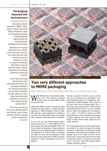
The WLCSP magne<strong>to</strong>meter BMM150.<br />
(Courtesy of Robert Bosch)<br />
“It’s been a question of how far you can push the<br />
limits of the package and its manufacture,” says<br />
Georg Bischopink, Bosch VP of engineering, who’s<br />
responsible for <strong>MEMS</strong> <strong>packaging</strong>. “We’ve found we<br />
can push further than we thought before. <strong>Two</strong> <strong>to</strong><br />
three years ago we thought that a 2 x 2mm 2 package<br />
was the absolute limit, but now 2 x 2mm 2 is standard<br />
and our newest mold package with wire bonding is<br />
1.2 x 1.5mm 2 .” The IDM can improve the <strong>MEMS</strong><br />
design and tune its volume manufacturing processes<br />
<strong>to</strong> tighter <strong>to</strong>lerances, while also driving the ASIC<br />
design <strong>to</strong> better handle smaller signals from the<br />
smaller structures.<br />
Then it works closely with its assembly subcontrac<strong>to</strong>rs<br />
<strong>to</strong> simulate all the effects and adjust the molding<br />
compounds, temperatures and pressures <strong>to</strong> manage<br />
the stresses. It has outsourced all assembly of mold<br />
packages since the mid 1990s <strong>to</strong> its own lines at<br />
subcontrac<strong>to</strong>rs in Asia, starting with mold technology<br />
for au<strong>to</strong>motive sensors. “It would be <strong>to</strong>o expensive<br />
<strong>to</strong> do it in Germany,” notes Frank Schaefer, product<br />
manager, au<strong>to</strong>motive sensors.<br />
6<br />
3 D P a c k a g i n g
I S S U E N ° 2 6<br />
F e b r u a r y 2 0 1 3<br />
The company expects stacking of chips with wire<br />
bonding <strong>to</strong> continue <strong>to</strong> be its main approach even as<br />
sensors move increasingly <strong>to</strong> multichip combinations<br />
in single packages, that integrate some combination<br />
of accelerometers, gyroscopes, and magne<strong>to</strong>meters<br />
for full motion sensing, plus a microcontroller for<br />
more sophisticated processing and perhaps a RF<br />
chip for wireless. That means more thinning of the<br />
chips — of the CMOS more readily than the more<br />
sensitive <strong>MEMS</strong> — for triple stacking <strong>to</strong> still stay<br />
under the 1mm package height limit expected for<br />
mobile consumer products. “Our roadmap is that<br />
the standard LGA works fine,” says Schaefer, arguing<br />
that direct wafer-<strong>to</strong>-wafer or chip-<strong>to</strong>-wafer bonding<br />
or bumping won’t work well with multiple chips of<br />
<strong>very</strong> <strong>different</strong> sizes. “And TSV is <strong>to</strong>o expensive,” he<br />
notes. “We’re still fine with wire bonding.”<br />
On the au<strong>to</strong>motive side, cus<strong>to</strong>mers are discussing<br />
alternatives <strong>to</strong> SOIC packages, but concern for<br />
the reliability of the soldering in smaller packages<br />
outweighs the limited interest in reducing size. Here<br />
<strong>to</strong>o the main emphasis is on pushing the conventional<br />
technology, <strong>to</strong> eliminate pre-mold and optimize the<br />
molding compound and process specifications.<br />
Bosch has, however, recently made its first foray<br />
in<strong>to</strong> wafer-level chip sized <strong>packaging</strong>, with its<br />
latest tiny 3-axis magne<strong>to</strong>meter. The magnetic<br />
sensor elements are integrated in<strong>to</strong> the ASIC and<br />
solder bumps added on <strong>to</strong>p. The combination of<br />
ASIC and solder bumps has a height of 0.6mm.<br />
“This is our only WL CSP so far without any mold,”<br />
notes Bischopink, suggesting some caution about<br />
how widely applicable the technology will be, as it<br />
requires more robust sensors than for an LGA.<br />
Silex pushes low-density TSVs<br />
<strong>to</strong> next generation<br />
At the other end of the spectrum, the leading pureplay<br />
<strong>MEMS</strong> foundry Silex Microsystems has seen<br />
double digit growth in recent years, <strong>to</strong> close <strong>to</strong><br />
$40 million in annual sales, in large part by providing<br />
its small fabless <strong>MEMS</strong> cus<strong>to</strong>mers with an established<br />
through-silicon via interconnect <strong>to</strong> distinguish their<br />
products. Peter Himes, Silex VP of marketing and<br />
strategic alliances, says that about half its cus<strong>to</strong>mers<br />
now use its low density, all-silicon TSV process,<br />
either for an interposer between the <strong>MEMS</strong> and ASIC<br />
chips, or as an element of the <strong>MEMS</strong> for its I/O <strong>to</strong><br />
the ASIC or the board, allowing reduction of the pad<br />
area for smaller, lower cost devices. These via-first<br />
connections are made in full-thickness wafers by<br />
isolating plugs of low-resistance silicon by etching<br />
around them and filling the trench with dielectric.<br />
TSVs for <strong>MEMS</strong> are generally low density, with typical<br />
pitches of 100 <strong>to</strong> 200µm and anywhere from 2 <strong>to</strong> 20<br />
TSVs per device, on full-thickness wafers that avoid<br />
the need for thin wafer handling or special carriers,<br />
a much simpler and lower cost solution than the thin<br />
interposers for high density ICs.<br />
The Swedish company is now introducing a new<br />
generation of copper-filled vias in full thickness<br />
wafers, pushing the low-density TSV approach<br />
<strong>to</strong>wards smaller pitch and lower resistance, <strong>to</strong> extend<br />
application <strong>to</strong> smaller <strong>MEMS</strong> devices, and potentially<br />
<strong>to</strong> other analog, mixed signal, LED and power devices<br />
that also need 10s or 100s, not 1000s of vias. These<br />
90µm-diameter copper vias use technology licensed<br />
from Swedish supplier ÅAC Microtec. A small etch<br />
from the front and a deep etch from the back create<br />
a waist in the middle of the full-wafer via profile that<br />
serves as a locking pin <strong>to</strong> prevent the relatively large<br />
plug from popping out during temperature cycling.<br />
The copper filling has a hollow core <strong>to</strong> compensate<br />
for the TCE mismatch between the copper and the<br />
silicon <strong>to</strong> improve reliability.<br />
Next on the roadmap is a 50µm version, and a<br />
technology <strong>to</strong> build embedded passives in<strong>to</strong> the<br />
silicon along with the copper vias, developed in<br />
conjunction with an European-funded research<br />
program. An induc<strong>to</strong>r, for example, could be built<br />
through the vertical TSV <strong>to</strong> take up less substrate<br />
surface area than the usual horizontal coil, providing<br />
high inductance-per-unit-area integrated passive<br />
capabilities.<br />
Silex is currently working <strong>to</strong> develop complete<br />
characterization of the thermal and frequency and<br />
other properties for the final <strong>packaging</strong> and assembly<br />
of these wafer-level TSV stacks, <strong>to</strong> offer cus<strong>to</strong>mers a<br />
complete engineered solution of the whole system <strong>to</strong><br />
ease design and speed transfer <strong>to</strong> production of the<br />
packaged device.<br />
Paula Doe for Yole Développement<br />
(Courtesy of Silex Microsystems)<br />
“Our roadmap is<br />
that the standard<br />
LGA works fine.<br />
We’re still fine with<br />
wire bonding,”<br />
says Dr Frank<br />
Schaefer, Bosch.<br />
Dr. Georg Bischopink, Vice<br />
President, Bosch Engineering<br />
Sensors for External Cus<strong>to</strong>mers<br />
and Sensor Packages, Bosch<br />
Georg hold in 1992 a Ph. D. in<br />
semiconduc<strong>to</strong>r physics, University<br />
of Freiburg, Germany. He has<br />
worked at Bosch since 1992 at various positions such as<br />
Section Manager - Development <strong>MEMS</strong> Sensor Products,<br />
Direc<strong>to</strong>r, Bosch <strong>MEMS</strong>-Production or Vice President, Bosch<br />
Corporate Research Microsystem-Technology.<br />
Peter Himes, VP Marketing<br />
& Strategic Alliances, Silex<br />
Microsystems<br />
Peter has over 25 years’ experience<br />
in helping startups and public<br />
companies establish their strategic<br />
direction and industry position.<br />
Experienced in IC and <strong>MEMS</strong> alike,<br />
Peter has held VP of Sales and/or Marketing positions<br />
at QuickSil, SiTime, and Winbond Corporations.<br />
Dr. Frank Schaefer, Senior<br />
Manager for Product<br />
Management Au<strong>to</strong>motive<br />
<strong>MEMS</strong>, Bosch<br />
Franck hold in 1999 a Ph.D. in<br />
semiconduc<strong>to</strong>r physics, University<br />
of Wuerzburg, Germany. He has<br />
been working with Bosch since 1999 at various positions<br />
in the field of <strong>MEMS</strong>. Since 2012, he is head of product<br />
management for au<strong>to</strong>motive <strong>MEMS</strong> sensors.<br />
3 D P a c k a g i n g<br />
7
F e b r u a r y 2 0 1 3 I S S U E N ° 2 6<br />
“Instead of putting<br />
the high value<br />
ASIC on a blank<br />
silicon interposer<br />
with vias and<br />
interconnects,<br />
we could put the<br />
pho<strong>to</strong>nics on the<br />
interposer and<br />
connect it directly<br />
<strong>to</strong> the upstairs<br />
die,” says Chris<br />
Bergey, Luxtera.<br />
INDUSTRY REVIEW – FOCUS ON SILICON PHOTONICS PACKAGING<br />
Silicon pho<strong>to</strong>nics looks for 2.5D<br />
assembly at OSATs<br />
Though silicon pho<strong>to</strong>nics has so far relied on one-chip integration of optics with<br />
electronics <strong>to</strong> start <strong>to</strong> get real traction in the data communications market, sec<strong>to</strong>r<br />
pioneer Luxtera sees the evolving <strong>packaging</strong> technology for heterogeneous 2.5D<br />
integration as the next generation solution <strong>to</strong> scale integrated pho<strong>to</strong>nics <strong>to</strong> high<br />
volume production. The company is working <strong>to</strong> build up a scalable back end silicon<br />
pho<strong>to</strong>nics infrastructure with OSATs and assembly and test <strong>to</strong>ol suppliers.<br />
Silicon pho<strong>to</strong>nics is still a small emerging<br />
market, but growing demand for high speed<br />
data communication is starting <strong>to</strong> spur serious<br />
interest. Yole Développement sees silicon pho<strong>to</strong>nic<br />
systems sales of some $215 million by 2017. The<br />
sec<strong>to</strong>r got a recent boost when Facebook announced<br />
plans <strong>to</strong> move <strong>to</strong> silicon pho<strong>to</strong>nics for its server<br />
interconnect, <strong>to</strong> enable disaggregation of computing<br />
in<strong>to</strong> separate units for more efficient sharing of<br />
memory among multiple processors. Leading supplier<br />
Luxtera says it has shipped more than half a million of<br />
the optics-and-transis<strong>to</strong>rs-on-silicon devices <strong>to</strong> date,<br />
primarily for active optical cables in data centers, and<br />
sees demand for >10M units a year by 2016.<br />
One key enabler of this growth will be moving from<br />
the electrical system-on-a-chip approach <strong>to</strong> an<br />
electrical and optical system in a package solution,<br />
made possible by the recent advances in 3D<br />
<strong>packaging</strong> technology. “The silicon infrastructure’s<br />
development of 2.5D heterogeneous integration is a<br />
key technology path forward for pho<strong>to</strong>nics,” says Chris<br />
Bergey, Luxtera VP of marketing. “Instead of putting<br />
the high value ASIC on a blank silicon interposer with<br />
vias and interconnects, we could put the pho<strong>to</strong>nics on<br />
the interposer and connect it directly <strong>to</strong> the upstairs<br />
die. This allows the silicon <strong>to</strong> have optical I/O with<br />
much lower system power consumption, terabits of<br />
speed and >100 meters of reach.” Cisco Systems<br />
recently similarly announced that it was pro<strong>to</strong>typing<br />
such a 2.5D silicon interposer solution.<br />
Integrating optics in<strong>to</strong> electronics for higher speed<br />
transmission requires optical waveguides, modula<strong>to</strong>rs<br />
and receivers in silicon, integrated with CMOS<br />
transis<strong>to</strong>rs, which silicon pho<strong>to</strong>nics suppliers now<br />
make on a single chip. More complicated is getting the<br />
optical power supply of light in<strong>to</strong> the system, whether<br />
by also integrating III-V laser devices in<strong>to</strong> the silicon,<br />
or bonding on the compound semiconduc<strong>to</strong>r devices,<br />
or micro <strong>packaging</strong> a <strong>MEMS</strong> mirror device on <strong>to</strong>p, or<br />
by connecting a separate laser component <strong>to</strong> the chip<br />
by optical fiber. Getting the light out of the system<br />
means connecting the chip <strong>to</strong> optical fiber.<br />
Integrating the diverse optics and electronics at the<br />
package level could be a simpler volume production<br />
solution, now that 2.5D heterogeneous integration<br />
technology for short, fast connections is emerging. A<br />
silicon pho<strong>to</strong>nics foundry could process the large<br />
pho<strong>to</strong>nic device, making waveguides, modula<strong>to</strong>rs,<br />
receivers, optical I/Os <strong>to</strong> connect <strong>to</strong> the ASIC, and<br />
Optical coupler:<br />
interfaces between<br />
interposer<br />
and MT-ferrules<br />
Optical fibers provide high-speed<br />
interconnect and provide supply<br />
of DC light <strong>to</strong> transmitters<br />
Pho<strong>to</strong>nic<br />
Interposer<br />
Package Substrate:<br />
• High & low speed IO<br />
• Power supply and<br />
• Mechanical support<br />
<strong>to</strong> interposer<br />
Heat sink mounted<br />
on package<br />
MT-Ferrules as example<br />
for pluggable fiber (MCF)<br />
interconnect<br />
Optical ASIC foor plan & <strong>packaging</strong>. (Courtesy of Luxtera)<br />
8<br />
3 D P a c k a g i n g
I S S U E N ° 2 6<br />
F e b r u a r y 2 0 1 3<br />
Optical ASIC foor plan & <strong>packaging</strong>. (Courtesy of Luxtera)<br />
adding a limited number of TSVs for power and ground<br />
<strong>to</strong> the printed circuit board. The interposer wafer could<br />
be full thickness or thinned, depending on application<br />
requirements. A packager could then micro bump an<br />
advanced CMOS control die and a little glass connec<strong>to</strong>r<br />
component on <strong>to</strong> the pho<strong>to</strong>nic/interposer-- either chipon-chip<br />
or chip-on-wafer--then plug in and align the<br />
optical fiber bundle <strong>to</strong> that connec<strong>to</strong>r.<br />
“Very little new needs <strong>to</strong> be developed beyond<br />
the natural evolution of the mainstream 2.5D<br />
<strong>packaging</strong> processes,” argues Bergey. The vias<br />
would need <strong>to</strong> be made through SOI wafers for the<br />
pho<strong>to</strong>nics/interposer, but there don’t appear <strong>to</strong> be<br />
major issues there. Assembly equipment will need<br />
<strong>to</strong> be modified <strong>to</strong> <strong>very</strong> precisely align the glass plug<br />
<strong>to</strong> the pho<strong>to</strong>nics substrate, and then <strong>to</strong> align the<br />
fiber in<strong>to</strong> the connec<strong>to</strong>r. The required precision<br />
is on the order of that of copper pillar bumping,<br />
more precise than that for flip chip. Bergey figures<br />
commercial die attach <strong>to</strong>ols could be cus<strong>to</strong>mized <strong>to</strong><br />
do the job, doing first pass alignment by machine<br />
vision, then running light though the fibers for final<br />
optical alignment.<br />
Luxtera has been busy finding partners <strong>to</strong> help in its<br />
strategy of leveraging the existing semiconduc<strong>to</strong>r<br />
manufacturing infrastructure <strong>to</strong> ramp silicon<br />
pho<strong>to</strong>nics quickly <strong>to</strong> low-cost volume production,<br />
including for <strong>packaging</strong>, assembly and test. It has<br />
designed its pho<strong>to</strong>nics <strong>to</strong> use standard processes and<br />
<strong>to</strong>ols, and is licensing its technology <strong>to</strong> encourage<br />
others <strong>to</strong> develop products <strong>to</strong> add <strong>to</strong> the volumes<br />
as well. The company is now producing on 200mm<br />
wafers at Freescale Semiconduc<strong>to</strong>r, and developing<br />
a 300mm process at STMicroelectronics. ST plans<br />
<strong>to</strong> design and manufacture its own products for its<br />
cus<strong>to</strong>mers with the process, as well as fab devices<br />
for Luxtera. Luxtera also has supplied its process <strong>to</strong><br />
OpSIS for an open foundry service with design kit<br />
and multi-product wafers run at IME in Singapore<br />
and at Luxtera’s own fab, <strong>to</strong> help bring down the<br />
cost of pho<strong>to</strong>nics development for other users. It’s<br />
working with an OSAT <strong>to</strong> build a standard process<br />
for optical attach and test. It has partnered with<br />
Tokyo Electron <strong>to</strong> cus<strong>to</strong>mize a standard probe <strong>to</strong>ol<br />
for high speed wafer-scale optical testing, with fast<br />
alignment using prober cameras. After developing<br />
the needed volume technologies with the first key<br />
partner, Luxtera expects that partner <strong>to</strong> sell <strong>to</strong> other<br />
users as well, while Luxtera rolls the technologies<br />
out <strong>to</strong> more suppliers <strong>to</strong> create a more robust<br />
supply chain. “There’s a whole ecosystem that has<br />
<strong>to</strong> be built out as systems move from copper <strong>to</strong><br />
optical interfaces for 25Gbps and beyond—it’s a big<br />
transition,” says Bergey.<br />
Paula Doe for Yole Développement<br />
Chris Bergey,<br />
Vice President<br />
of Marketing,<br />
Luxtera<br />
Prior <strong>to</strong> joining<br />
Luxtera, Chris was<br />
a Vice president at<br />
Broadcom, responsible for establishing<br />
and managing Broadcom’s WLAN<br />
combo business, which he grew<br />
in<strong>to</strong> one of Broadcom’s largest lines<br />
of business. Prior <strong>to</strong> spending nine<br />
years at Broadcom, Bergey worked<br />
for Multilink Technology Corporation<br />
and Advanced Micro Devices. Chris<br />
received his MBA from the University<br />
of Maryland and a BS in Electrical and<br />
Computer Engineering from Drexel<br />
University.<br />
3 D P a c k a g i n g<br />
9
F e b r u a r y 2 0 1 3 I S S U E N ° 2 6<br />
INDUSTRY REVIEW – FOCUS ON POWER DEVICE PACKAGING<br />
New <strong>packaging</strong> technology<br />
and new business models impact<br />
power module design<br />
Potential volume markets in alternative energy applications have attracted<br />
investment in<strong>to</strong> both new <strong>packaging</strong> technologies and new business models that<br />
could have a big impact on the power device market. We check in with International<br />
Rectifier on technology for replacing wire bonding with modular solderable<br />
components, and with iQXPRZ on the rise of the fabless/foundry option.<br />
The potentially high volumes and extreme<br />
performance demands of the hybrid and<br />
electric vehicle market will have significant<br />
impact on power device technology. One recent<br />
example of the innovation being driven by this<br />
market is International Rectifier’s new modular<br />
IGBT and diode co-pack building block that can<br />
be surface mounted in <strong>different</strong> combinations,<br />
simplifying power module construction and allowing<br />
systems makers <strong>to</strong> more easily create their own<br />
optimized power circuit <strong>to</strong>pologies.<br />
IR has replaced the wire bonds with solderable<br />
metal on both sides of the thin IGBT and diode<br />
dies, and attached both <strong>to</strong> a direct bonded copper<br />
substrate. These pre-assembled and pre-tested<br />
building blocks are then attached <strong>to</strong> a DBC—singly<br />
or in multiples, either face up, or face down flip-chip<br />
style for shorter connections and flexible design.<br />
Eliminating the wire bonds improves reliability<br />
and makes a more compact device, while the<br />
IGBT and diode dies with solderable metal on both sides can be easily assembled in<strong>to</strong> co-packs<br />
and modules. (Courtesy of International Rectifier)<br />
double-sided cooling signifiantly improves thermal<br />
performance. After attaching the leadframe, this<br />
compact unit is then overmolded. Compared <strong>to</strong><br />
a conventional module wirebonded in a gel-sealed<br />
plastic package, this process adds a <strong>to</strong>p layer of<br />
DBC, but eliminates the wirebonds, gel and base<br />
plate, although a base plate can be added as an<br />
option.<br />
Jack Marcinkowski, Sr. Technical Marketing and<br />
Applications Manager for International Rectifier’s<br />
Au<strong>to</strong>motive Business Unit, says this buildingblock<br />
approach significantly reduces overall<br />
system cost, by improving mechanical, electrical<br />
and thermal performance, but especially by<br />
providing a standardized and tested building block<br />
that simplifies power module cus<strong>to</strong>mization and<br />
assembly and improves yields. IR will both use the<br />
technology in its own modules and sell the devices<br />
<strong>to</strong> outside cus<strong>to</strong>mers.<br />
“This intermediate co-pack fills the gap between<br />
discretes and modules,” he says, noting that the<br />
compact modules can replace a number of discrete<br />
packaged devices. “There’s no precedent in the<br />
industry. Manufacturers can use the co-pack like<br />
a surface-mounted component <strong>to</strong> create their own<br />
optimized cus<strong>to</strong>m <strong>to</strong>pology, instead of trying <strong>to</strong><br />
design their system around an existing commercial<br />
module.” The compact module is reportedly<br />
roughly half the size and a quarter of the weight of<br />
a similarly-rated wire-bonded gel package, opening<br />
design possibilities such as putting the inverter<br />
inside the electric mo<strong>to</strong>r housing, for example.<br />
Key <strong>to</strong> the development was selecting proper<br />
device metallization, die attach, materials with<br />
well matched thermal expansion properties,<br />
and devising a high yielding manufacturing<br />
process. The company says the payoff is major<br />
improvements in performance for EV/HEV inverter<br />
demands. Marcinkowski reports the devices have<br />
held up through some one million thermal cycles so<br />
far in company tests, while wirebonds—the most<br />
common failure mechanism for power devices—<br />
may start <strong>to</strong> crack or delaminate at 100,000 cycles.<br />
10 3 D P a c k a g i n g
I S S U E N ° 2 6<br />
F e b r u a r y 2 0 1 3<br />
The lower resistance of these direct soldered<br />
interconnects also reduces losses and means about<br />
a 5%-7% decrease in power dissipation, he says.<br />
The DBC sandwiching the dies provide doublesided<br />
cooling capability, though initial applications<br />
using conventional heat sink <strong>approaches</strong> won’t get<br />
the full advantage of it. “To switch <strong>to</strong> double-sided<br />
cooling, the mechanical design of the inverter<br />
cooling system will have <strong>to</strong> be adapted,” notes<br />
Marcinkowski. “But it will soon be necessary <strong>to</strong><br />
do that, <strong>to</strong> improve the heat transfer from more<br />
compact packages.” The IBGT-and-diode co-pack<br />
can run at a 25°C higher junction temperature<br />
than the current typical 150°C. With the doublesided<br />
cooling, IR figures the device can potentially<br />
achieve as much as 80% higher current rating<br />
than a single-side cooled device with a maximum<br />
junction temperature rating of 150°C.<br />
Fabless iQXPRZ designs power<br />
modules for foundry production<br />
Also relatively new <strong>to</strong> the traditionally IDMdriven<br />
power device business is the rise of fabless<br />
companies and foundries, also expanding the<br />
options for module design and manufacture. The<br />
boom of investment in solar and wind energy in<br />
China attracted a crowd of new entrants <strong>to</strong> the<br />
market for inverters and their component power<br />
devices and modules. Many of these players had<br />
the expertise and capital <strong>to</strong> focus on only one step<br />
in what looked <strong>to</strong> be a big volume opportunity<br />
<strong>to</strong> bring down manufacturing costs in the power<br />
sec<strong>to</strong>r. Though the recent downturn in the<br />
renewable energy sec<strong>to</strong>r has hurt these suppliers,<br />
some are successfully expanding the power<br />
sec<strong>to</strong>r’s options for lower cost production.<br />
One of these fabless module design companies<br />
now breaking in<strong>to</strong> the European market is QXPRZ<br />
(pronounced IQ Express). The Manila-based<br />
company works closely with a local established<br />
power device assembly subcontrac<strong>to</strong>r <strong>to</strong> pro<strong>to</strong>type<br />
and manufacture the devices in low volume. The<br />
business got its start in the alternative energy<br />
bubble five years ago, designing complex power<br />
modules using off-the-shelf discrete devices<br />
SuperSOT (Courtesy of iQXPRZ Power)<br />
for small inverter makers. With the plunge in<br />
renewable energy demand, the company has lately<br />
been focusing largely on smart power modules for<br />
the home appliance sec<strong>to</strong>r, integrating IC drivers<br />
with IGBTs and MOSFETs in<strong>to</strong> compact <strong>packaging</strong>.<br />
VP and COO Cherie Sasan says the company<br />
strategy is targets small companies who need<br />
complex cus<strong>to</strong>mized power modules in <strong>very</strong> small<br />
quantities, aiming <strong>to</strong> offer lower cost products<br />
than the technology-leading European module<br />
makers, but better quality than its fabless/foundry<br />
Chinese competi<strong>to</strong>rs. “Most of our cus<strong>to</strong>mers are in<br />
Europe,” says Sasan. “And most of our competition<br />
is in China. Most of our cus<strong>to</strong>mers have used<br />
Chinese products before they turned <strong>to</strong> us.”<br />
To make manufacture of the cus<strong>to</strong>m products more<br />
efficient, the company aims <strong>to</strong> use a standard<br />
plastic housing which has multiple <strong>different</strong> holes<br />
<strong>to</strong> accommodate <strong>different</strong> leads for <strong>different</strong><br />
products, and a standard leadframe inside, whose<br />
<strong>different</strong> pins can be connected or not as needed.<br />
It also sticks <strong>to</strong> conventional technologies, producing<br />
some legacy products obsoleted by the big IDMs.<br />
“We’re not innova<strong>to</strong>rs,” says Sasan, though she does<br />
note that the company is working on developing an<br />
alternative substrate material <strong>to</strong> AlN.<br />
Paula Doe for Yole Développement<br />
Jack Marcinkowski, Sr. Technical<br />
Marketing and Applications Manager,<br />
International Rectifier’s Au<strong>to</strong>motive<br />
Business Unit.<br />
Jack is responsible for development of<br />
power modules with focus on HEV and<br />
EV applications. Jack first joined IR in 2003<br />
as an Applications Design Manager working for the Au<strong>to</strong>motive<br />
Business Unit for 4 years and re-joined IR in July of 2011. Jack<br />
holds a MSEE degree from Technical University in Warsaw, Poland<br />
as well as an MBA degree from UCLA in Los Angeles, California.<br />
Cherie Sasan, Vice-president & COO,<br />
iQXPRZ Power<br />
Cherie worked in the semiconduc<strong>to</strong>r<br />
industry for more than 20 years. She<br />
joined iQXPRZ Power Inc in 2008 and is<br />
responsible for corporate strategy, business<br />
development and commercial operations.<br />
Prior joining iQXPRZ Power Inc, she was the Development<br />
Engineering Manager of Team Pacific Corporation. She holds<br />
a degree in Electronics and Communications Engineering from<br />
the Mapua Institute of Technology and is currently taking up<br />
MBA at the Ateneo de Manila-Regis University.<br />
3 D P a c k a g i n g<br />
11


