

Two very different approaches to MEMS packaging - I-Micronews
Two very different approaches to MEMS packaging - I-Micronews
Two very different approaches to MEMS packaging - I-Micronews

You also want an ePaper? Increase the reach of your titles
YUMPU automatically turns print PDFs into web optimized ePapers that Google loves.
I S S U E N ° 2 6<br />
F e b r u a r y 2 0 1 3<br />
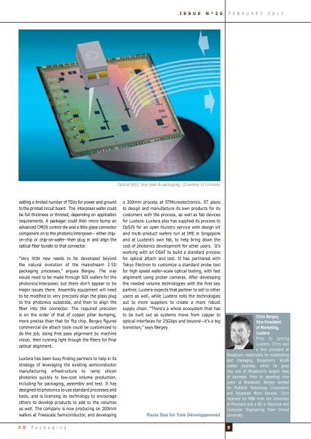
Optical ASIC foor plan & <strong>packaging</strong>. (Courtesy of Luxtera)<br />
adding a limited number of TSVs for power and ground<br />
<strong>to</strong> the printed circuit board. The interposer wafer could<br />
be full thickness or thinned, depending on application<br />
requirements. A packager could then micro bump an<br />
advanced CMOS control die and a little glass connec<strong>to</strong>r<br />
component on <strong>to</strong> the pho<strong>to</strong>nic/interposer-- either chipon-chip<br />
or chip-on-wafer--then plug in and align the<br />
optical fiber bundle <strong>to</strong> that connec<strong>to</strong>r.<br />
“Very little new needs <strong>to</strong> be developed beyond<br />
the natural evolution of the mainstream 2.5D<br />
<strong>packaging</strong> processes,” argues Bergey. The vias<br />
would need <strong>to</strong> be made through SOI wafers for the<br />
pho<strong>to</strong>nics/interposer, but there don’t appear <strong>to</strong> be<br />
major issues there. Assembly equipment will need<br />
<strong>to</strong> be modified <strong>to</strong> <strong>very</strong> precisely align the glass plug<br />
<strong>to</strong> the pho<strong>to</strong>nics substrate, and then <strong>to</strong> align the<br />
fiber in<strong>to</strong> the connec<strong>to</strong>r. The required precision<br />
is on the order of that of copper pillar bumping,<br />
more precise than that for flip chip. Bergey figures<br />
commercial die attach <strong>to</strong>ols could be cus<strong>to</strong>mized <strong>to</strong><br />
do the job, doing first pass alignment by machine<br />
vision, then running light though the fibers for final<br />
optical alignment.<br />
Luxtera has been busy finding partners <strong>to</strong> help in its<br />
strategy of leveraging the existing semiconduc<strong>to</strong>r<br />
manufacturing infrastructure <strong>to</strong> ramp silicon<br />
pho<strong>to</strong>nics quickly <strong>to</strong> low-cost volume production,<br />
including for <strong>packaging</strong>, assembly and test. It has<br />
designed its pho<strong>to</strong>nics <strong>to</strong> use standard processes and<br />
<strong>to</strong>ols, and is licensing its technology <strong>to</strong> encourage<br />
others <strong>to</strong> develop products <strong>to</strong> add <strong>to</strong> the volumes<br />
as well. The company is now producing on 200mm<br />
wafers at Freescale Semiconduc<strong>to</strong>r, and developing<br />
a 300mm process at STMicroelectronics. ST plans<br />
<strong>to</strong> design and manufacture its own products for its<br />
cus<strong>to</strong>mers with the process, as well as fab devices<br />
for Luxtera. Luxtera also has supplied its process <strong>to</strong><br />
OpSIS for an open foundry service with design kit<br />
and multi-product wafers run at IME in Singapore<br />
and at Luxtera’s own fab, <strong>to</strong> help bring down the<br />
cost of pho<strong>to</strong>nics development for other users. It’s<br />
working with an OSAT <strong>to</strong> build a standard process<br />
for optical attach and test. It has partnered with<br />
Tokyo Electron <strong>to</strong> cus<strong>to</strong>mize a standard probe <strong>to</strong>ol<br />
for high speed wafer-scale optical testing, with fast<br />
alignment using prober cameras. After developing<br />
the needed volume technologies with the first key<br />
partner, Luxtera expects that partner <strong>to</strong> sell <strong>to</strong> other<br />
users as well, while Luxtera rolls the technologies<br />
out <strong>to</strong> more suppliers <strong>to</strong> create a more robust<br />
supply chain. “There’s a whole ecosystem that has<br />
<strong>to</strong> be built out as systems move from copper <strong>to</strong><br />
optical interfaces for 25Gbps and beyond—it’s a big<br />
transition,” says Bergey.<br />
Paula Doe for Yole Développement<br />
Chris Bergey,<br />
Vice President<br />
of Marketing,<br />
Luxtera<br />
Prior <strong>to</strong> joining<br />
Luxtera, Chris was<br />
a Vice president at<br />
Broadcom, responsible for establishing<br />
and managing Broadcom’s WLAN<br />
combo business, which he grew<br />
in<strong>to</strong> one of Broadcom’s largest lines<br />
of business. Prior <strong>to</strong> spending nine<br />
years at Broadcom, Bergey worked<br />
for Multilink Technology Corporation<br />
and Advanced Micro Devices. Chris<br />
received his MBA from the University<br />
of Maryland and a BS in Electrical and<br />
Computer Engineering from Drexel<br />
University.<br />
3 D P a c k a g i n g<br />
9


